

Page 1
Dual-Channel Isolators with isoPower
Integrated DC-to-DC Converter, 50 mW
Data Sheet
FEATURES
Integrated isolated dc-to-dc converter
Regulated 5 V/10 mA output
Dual dc to 1 Mbps (NRZ) signal isolation channels
Narrow-body, 8-lead SOIC package
RoHS compliant
High temperature operation: 105°C
Precise timing characteristics
3 ns maximum pulse width distortion
3 ns maximum channel-to-channel matching
70 ns maximum propagation delay
High common-mode transient immunity: >25 kV/μs
Safety and regulatory approvals
UL recognition
2500 V rms for 1 minute, per UL 1577
CSA Component Acceptance Notice #5A
VDE certificate of conformity
DIN V VDE V 0884-10 (VDE V 0884-10):2006-12
V
= 560 V peak
IORM
GENERAL DESCRIPTION
The ADuM524x
integrated, isolated power. Based on the Analog Devices, Inc.,
iCoupler® technology, a chip scale dc-to-dc converter provides
up to 50 mW of regulated, isolated power at 5 V, which eliminates
the need for a separate isolated dc-to-dc converter in low power
isolated designs. The Analog Devices chip scale transformer
iCoupler technology is used both for the isolation of the logic
signals as well as for the dc-to-dc converter. The result is a small
form factor, total isolation solution.
The ADuM524x isolators provide two independent isolation
channels in a variety of channel configurations, operating from
a 5 V input supply. ADuM524x units can be used in combination
with other iCoupler products to achieve greater channel counts.
1
Protected by U.S. Patents 5,952,849; 6,873,065; and 7,075,329.
1
are dual-channel digital isolators with isoPower®
ADuM5240/ADuM5241/ADuM5242
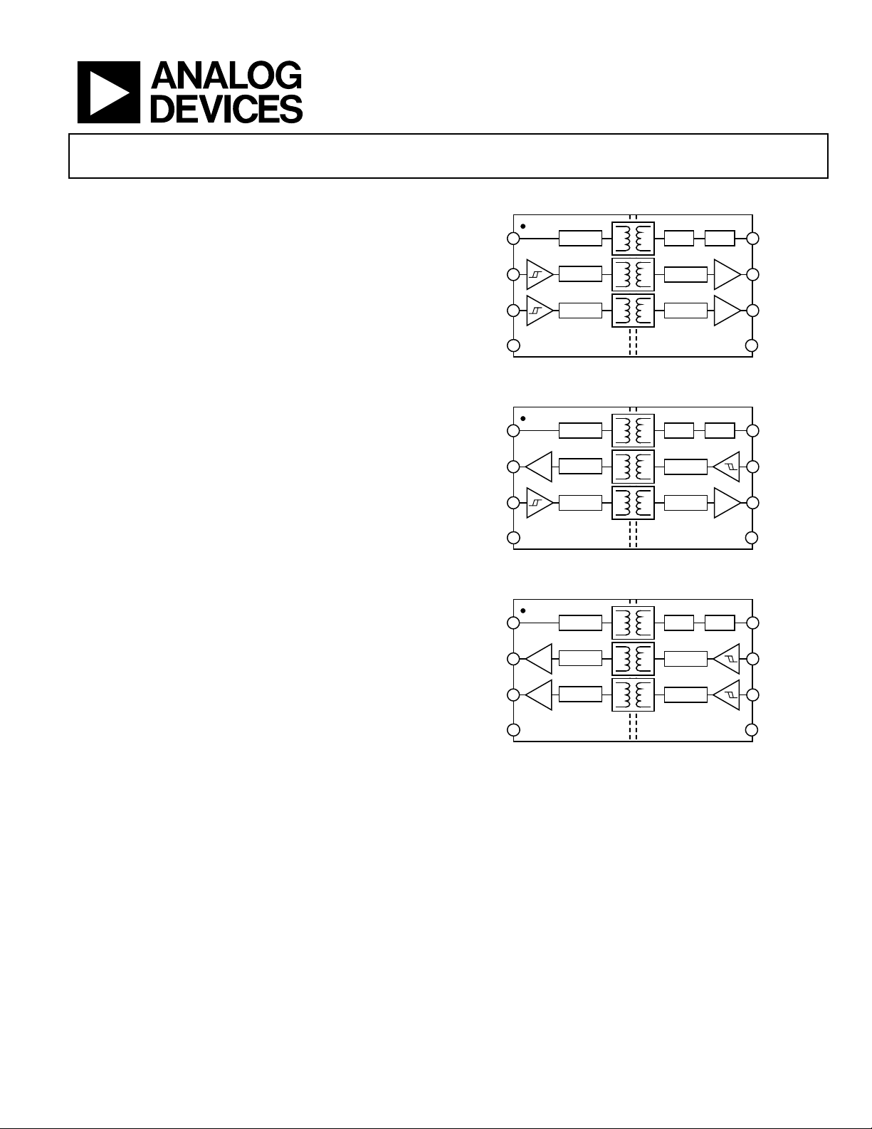
FUNCTIONAL BLOCK DIAGRAMS
V
V
V
GND
1
DD
2
IA
3
IB
4
OSC.
ENCODE
DECODE
DECODEENCODE
Figure 1. ADuM5240
V
V
V
GND
1
DD
2
OA
3
IB
4
OSC.
DECODE
Figure 2. ADuM5241
ENCODE
DECODEENCODE
V
V
GND
1
DD
2
OA
3
OB
4
OSC.
DECODE
DECODEV
Figure 3. ADuM5242
ENCODE
ENCODE
8
REG.RECT.
REG.RECT.
REG.RECT.
V
ISO
7
V
OA
6
V
OB
5
GND
ISO
8
V
ISO
7
V
IA
6
V
OB
5
GND
ISO
8
V
ISO
7
V
IA
6
V
IB
5
GND
ISO
06014-001
06014-002
06014-003
Rev. B
Information furnished by Analog Devices is believed to be accurate and reliable. However, no
responsibility is assumed by Analog Devices for its use, nor for any infringements of patents or other
rights of third parties that may result from its use. Specifications subject to change without notice. No
license is granted by implication or otherwise under any patent or patent rights of Analog Devices.
Trademarks and registered trademarks are the property of their respective owners.
One Technology Way, P.O. Box 9106, Norwood, MA 02062-9106, U.S.A.
Tel: 781.329.4700 www.analog.com
Fax: 781.461.3113 ©2007–2012 Analog Devices, Inc. All rights reserved.
Page 2

ADuM5240/ADuM5241/ADuM5242 Data Sheet
TABLE OF CONTENTS
Features .............................................................................................. 1
General Description ......................................................................... 1
Functional Block Diagrams ............................................................. 1
Revision History ............................................................................... 2
Specifications ..................................................................................... 3
Electrical Characteristics ............................................................. 3
Package Characteristics ............................................................... 5
Regulatory Information ............................................................... 5
Insulation and Safety-Related Specifications ............................ 5
DIN V VDE V 0884-10 (VDE V 0884-10) Insulation
Characteristics .............................................................................. 6
Recommended Operating Conditions ...................................... 6
Absolute Maximum Ratings ............................................................ 7
REVISION HISTORY
5/12—Rev. A to Rev. B
Created Hyperlink for Safety and Regulatory Approvals
Entry in Features Section ................................................................. 1
Change to PCB Layout Section ..................................................... 12
7/07—Rev. 0 to Rev. A
Updated VDE Certification Throughout ...................................... 1
Changes to Features .......................................................................... 1
Changes to Regulatory Information Section and Table 4 ........... 5
Changes to Table 5 and Figure 4 Caption ...................................... 6
Changes to Table 7 ............................................................................ 7
Added Table 8; Renumbered Sequentially .................................... 7
Added Insulation Lifetime Section .............................................. 13
3/07—Revision 0: Initial Version
ESD Caution...................................................................................7
Pin Configurations and Function Descriptions ............................8
Typical Performance Characteristics ........................................... 10
Applications Information .............................................................. 11
DC-to-DC Converter................................................................. 11
Propagation Delay-Related Parameters ................................... 11
DC Correctness and Magnetic Field Immunity ..................... 11
Thermal Analysis ....................................................................... 12
PCB Layout ................................................................................. 12
Increasing Available Power ....................................................... 13
Insulation Lifetime ..................................................................... 13
Outline Dimensions ....................................................................... 14
Ordering Guide .......................................................................... 14
Rev. B | Page 2 of 16
Page 3

Data Sheet ADuM5240/ADuM5241/ADuM5242
DC-to-DC Converter Enabled
ISO (SET )
ISO
ISO
ISO (max)
ISO
ISO
DD (max)
ISO
ISO
DD (Q)
ISO
DD (DISABLE)
DD (DISABLE)
ADuM5242
I
DD (DISABLE)
2.2
mA
VDD = 4.0 V
ISO (DISABLE)
ISO (DISABLE)
ISO (DISABLE)
DD (ENABLE)
DD (DISABLE)
ISO
ISO
OAL
OBL
SPECIFICATIONS
ELECTRICAL CHARACTERISTICS
All voltages are relative to their respective ground. All minimum/maximum specifications apply over the entire recommended operating
range, unless otherwise noted. All typical specifications are at T
Table 1.
Parameter Symbol Min Typ Max Unit Test Conditions
DC-TO-DC CONVERTER
DC to 1 Mbps Data Rate Logic signal frequency ≤ 1 MHz
Setpoint V
Maximum V
Output Current I
Noise1 250 mV p-p
Input Supply Current
At Maximum I
No Load I
Current I
Current I
DC-to-DC Converter Disabled
Primary Side Supply Input Current2
ADuM5240 I
ADuM5241 I
= 25°C, VDD = 5.0 V, V
A
4.5 5.2 5.5 V I
10 mA V
140 mA I
104 mA I
= 5.0 V, unless otherwise noted.
ISO
= 0 mA
= 4.5 V
= 10 mA
= 0 mA
3.3 mA VDD = 4.0 V
2.7 mA VDD = 4.0 V
Secondary Side Supply Input Current3
ADuM5240 I
ADuM5241 I
ADuM5242 I
DC-to-DC Conver ter Enable Threshold4 V
DC-to-DC Converter Disable Threshold4 V
2.6 mA
2.8 mA
3.0 mA
4.2 4.5 V
3.7 V
LOGIC SPECIFICATIONS
Logic Input Currents IIA, IIB −10 +0.01 +10 µA
Logic High Input Threshold VIH 0.7 (VDD or
V
)
Logic Low Input Threshold VIL 0.3 (VDD or
Logic High Output Voltages V
OAH
, V
OBH (VDD
or V
V
V
)
)
ISO
(VDD or V
) V IOx = −20 µA, VIx ≥ VIH
ISO
V
− 0.1
(VDD or V
− 0.5
Logic Low Output Voltages V
, V
0.0 0.1 V IOx = 20 µA, VIx ≤ VIL
)
(VDD or V
ISO
)
V IOx = −4 mA, VIx ≥ VIH
ISO
− 0.2
0.0 0.4 V IOx = 4 mA, VIx ≤ VIL
Rev. B | Page 3 of 16
Page 4

ADuM5240/ADuM5241/ADuM5242 Data Sheet
PHL
PLH
Pulse Width Distortion, |t
PLH
− t
PHL
|8
PWD
3
ns
CL = 15 pF, CMOS signal levels
PSK
Refresh Frequency
fr 1.0 MHz
OSC
Parameter Symbol Min Typ Max Unit Test Conditions
AC SPECIFICATIONS
Minimum Pulse Width5 PW 100 ns CL = 15 pF, CMOS signal levels
Maximum Data Rate6 1 Mbps CL = 15 pF, CMOS signal levels
Propagation Delay7 t
, t
25 70 ns CL = 15 pF, CMOS signal levels
Propagation Delay Skew8 t
Channel-to-Channel Matching,
Codirectional Channels
Channel-to-Channel Matching,
Opposing-Directional Channels
9
9
45 ns CL = 15 pF, CMOS signal levels
3 ns CL = 15 pF, CMOS signal levels
t
PSKCD
15 ns CL = 15 pF, CMOS signal levels
t
PSKCD
Output Rise/Fall Time (10% to 90%) tR/tF 2.5 ns CL = 15 pF, CMOS signal levels
Common-Mode Transient
Immunity at Logic High Output
Common-Mode Transient
Immunity at Logic Low Output
Switching Frequency f
1
Peak noise occurs at frequency corresponding to the refresh frequency (see the PCB Layout section).
2
I
supply current values are specified with no load present on the digital outputs.
DD (DISAB LE)
3
I
supply current values are specified with no load present on the digital outputs and power sourced by an external supply.
ISO (DISABLE)
4
Enable/disable threshold is the VDD voltage at which the internal dc-to-dc converter is enabled/disabled.
5
The minimum pulse width is the shortest pulse width at which the specified pulse width distortion is guaranteed.
6
The maximum data rate is the fastest data rate at which the specified pulse width distortion and V
7
t
propagation delay is measured from the 50% level of the falling edge of the VIx signal to the 50% level of the falling edge of the VOx signal. t
PHL
measured from the 50% level of the rising edge of the V
8
t
is the magnitude of the worst-case difference in t
PSK
load within the recommended operating conditions.
9
Channel-to-channel matching is the absolute value of the difference in propagation delays between the two channels when operated with identical loads.
|CMH| 25 35 kV/µs VIx = VDD, V
, VCM = 1000 V,
ISO
transient magnitude = 800 V
|CML| 25 35 kV/µs VIx = 0 V, VCM = 1000 V,
transient magnitude = 800 V
300 MHz
supply voltage is guaranteed.
ISO
signal to the 50% level of the rising edge of the VOx signal.
Ix
and/or t
PHL
that is measured between units at the same operating temperature, supply voltages, and output
PLH
propagation delay is
PLH
Rev. B | Page 4 of 16
Page 5

Data Sheet ADuM5240/ADuM5241/ADuM5242
Resistance (Input-to-Output)
R
I-O
1012 Ω
I-O
Single/basic insulation, 2500 V rms
Basic insulation per CSA 60950-1-03
Reinforced insulation, 560 V peak
PACKAGE CHARACTERISTICS
Table 2.
Parameter Symbol Min Typ Max Unit Test Conditions
Capacitance (Input-to-Output) C
1.0 pF f = 1 MHz
Input Capacitance CI 4.0 pF
IC Junction-to-Air Thermal Resistance θJA 80 °C/W
REGULATORY INFORMATION
The ADuM524x are approved by the organizations listed in Table 3. Refer to Table 8 and the Insulation Lifetime section for details
regarding recommended maximum working voltages for specific cross-isolation waveforms and insulation levels.
Table 3.
UL CSA VDE
Recognized under 1577
Component Recognition Program
isolation rating
1
Approved under CSA Component
Acceptance Notice #5A
and IEC 60950-1, 400 V rms (566 V peak)
Certified according to DIN V VDE V 0884-10
(VDE V 0884-10):2006-122
maximum working voltage
File E214100 File 205078 File 2471900-4880-0001
1
In accordance with UL 1577, each ADuM524x is proof-tested by applying an insulation test voltage ≥ 3000 V rms for 1 second (current leakage detection limit = 5 µA).
2
In accordance with DIN V VDE V 0884-10, each ADuM524x is proof-tested by applying an insulation test voltage ≥ 1050 V peak for 1 sec (partial discharge detection
limit = 5 pC). The asterisk (*) marking branded on the component designates DIN V VDE V 0884-10
approval.
INSULATION AND SAFETY-RELATED SPECIFICATIONS
Table 4.
Parameter Symbol Value Unit Conditions
Rated Dielectric Insulation Voltage 2500 V rms 1-minute duration
Minimum External Air Gap (Clearance) L(I01) 4.90 min mm Measured from input terminals to output
terminals, shortest distance through air
Minimum External Tracking (Creepage) L(I02) 4.01 min mm Measured from input terminals to output
terminals, shortest distance path along body
Minimum Internal Gap (Internal Clearance) 0.017 min mm Insulation distance through insulation
Tracking Resistance (Comparative Tracking Index) CTI >175 V DIN IEC 112/VDE 0303 Part 1
Isolation Group IIIa Material Group (DIN VDE 0110, 1/89, Table 1)
Maximum Working Voltage Compatible with
50-Year Service Life
V
425 V peak Continuous peak voltage across the
IORM
isolation barrier
Rev. B | Page 5 of 16
Page 6

ADuM5240/ADuM5241/ADuM5242 Data Sheet
DIN V VDE V 0884-10 (VDE V 0884-10) INSULATION CHARACTERISTICS
This isolator is suitable for reinforced isolation only within the safety limit data. Maintenance of the safety data is ensured by protective
circuits.
Table 5.
Description Conditions Symbol Characteristic Unit
Installation Classification per DIN VDE 0110
For Rated Mains Voltage ≤ 150 V rms I to IV
For Rated Mains Voltage ≤ 300 V rms I to III
Climatic Classification 40/105/21
Pollution Degree (DIN VDE 0110, Table 1) 2
Maximum Working Insulation Voltage V
Input-to-Output Test Voltage, Method b1
× 1.875 = VPR, 100% production
V
IORM
= 1 sec, partial discharge < 5 pC
test, t
m
Input-to-Output Test Voltage, Method a VPR
After Environmental Tests Subgroup 1
× 1.6 = VPR, tm = 60 sec, partial
V
IORM
discharge < 5 pC
After Input and/or Safety Test Subgroup 2 and Subgroup 3
× 1.2 = VPR, tm = 60 sec, partial
V
IORM
discharge < 5 pC
Highest Allowable Overvoltage Transient overvoltage, tTR = 10 seconds VTR 4000 V peak
Safety-Limiting Values
Maximum value allowed in the event of
a failure; see Figure 4
Case Temperature TS 150 °C
Supply Current IS1 312 mA
Insulation Resistance at TS V
= 500 V RS >109 Ω
IO
350
RECOMMENDED OPERATING CONDITIONS
424 V peak
IORM
795 V peak
V
PR
680 V peak
510 V peak
300
250
CURRENT (mA)
200
DD
150
100
50
SAFE OPERATING V
0
0200
Figure 4. Thermal Derating Curve, Dependence of Safety-Limiting
Values on Case Temperature, per DIN V VDE V 0884-10
50 100 150
AMBIENT TEMPERATURE (°C)
Table 6.
Parameter Value
Operating Temperature Range (TA) −40°C to +105°C
Supply Voltages1
VDD, DC-to-DC Converter Enabled 4.5 V to 5.5 V
VDD, DC-to-DC Converter Disabled (VDD) 2.7 V to 4.0 V
V
, DC-to-DC Converter Disabled (V
ISO
) 2.7 V to 5.5 V
ISO
Input Signal Rise/Fall Time 1.0 ms
Input Supply Slew Rate 10 V/ms
1
06014-004
All voltages are relative to their respective ground.
Rev. B | Page 6 of 16
Page 7

Data Sheet ADuM5240/ADuM5241/ADuM5242
Ambient Operating Temperature Range (TA)
−40°C to +105°C
ISO
DD
ISO
(VDD or V
ISO
) + 0.5 V
ABSOLUTE MAXIMUM RATINGS
Table 7.
Parameter Rating
Storage Temperature Range (TST) −55°C to +150°C
Supply Voltages (VDD, V
)1 −0.5 V to +7.0 V
Input Voltage ( VIA, VIB)1 −0.5 V to
(V
or V
) + 0.5 V
Output Voltage (VOA, VOB)1 −0.5 V to
Stresses above those listed under Absolute Maximum Ratings
may cause permanent damage to the device. This is a stress
rating only; functional operation of the device at these or any
other conditions above those indicated in the operational
section of this specification is not implied. Exposure to absolute
maximum rating conditions for extended periods may affect
device reliability.
Average Output Current per Pin (IO)2 −18 mA to +18 mA
ESD CAUTION
Common-Mode Transients (|CM|)3 −100 kV/µs to
+100 kV/µs
1
All voltages are relative to their respective ground.
2
See Figure 4 for maximum rated current values for various temperatures.
3
Refers to common-mode transients across the insulation barrier. Common-
mode transients exceeding the Absolute Maximum Ratings may cause
latch-up or permanent damage.
1
Table 8. Maximum Continuous Working Voltage
Parameter Max Unit Constraint
AC Voltage, Bipolar Waveform 425 V peak 50-year minimum lifetime
AC Voltage, Unipolar Waveform
Basic Insulation 566 V peak Maximum approved working voltage per IEC 60950-1
Reinforced Insulation 560 V peak Maximum approved working voltage per VDE V 0884-10
DC Voltage
Basic Insulation 566 V peak Maximum approved working voltage per IEC 60950-1
Reinforced Insulation 560 V peak Maximum approved working voltage per VDE V 0884-10
1
Refers to continuous voltage magnitude imposed across the isolation barrier. See the Insulation Lifetime section for more details.
Rev. B | Page 7 of 16
Page 8

ADuM5240/ADuM5241/ADuM5242 Data Sheet
06014-009
V
DD
1
V
IA
2
V
IB
3
GND
4
V
ISO
8
V
OA
7
V
OB
6
GND
ISO
5
ADuM5240
TOP VIEW
(Not to Scale)
Pin
06014-010
V
DD
1
V
OA
2
V
IB
3
GND
4
V
ISO
8
V
IA
7
V
OB
6
GND
ISO
5
ADuM5241
TOP
VIEW
(Not to Scale)
06014-011
V
DD
1
V
OA
2
V
OB
3
GND
4
V
ISO
8
V
IA
7
V
IB
6
GND
ISO
5
ADuM5242
TOP VIEW
(Not to Scale)
Pin
PIN CONFIGURATIONS AND FUNCTION DESCRIPTIONS
Figure 5. ADuM5240 Pin Configuration
Table 9. ADuM5240 Pin Function Descriptions
No.
Mnemonic Description
1 VDD Supply Voltage for Isolator Primary Side,
4.5 V to 5.5 V (DC-to-DC Enabled) and
2.7 V to 4.0 V (DC-to-DC Disabled).
2 VIA Logic Input A.
3 VIB Logic Input B.
4 GND Ground. Ground reference for isolator
primary side.
5 GND
Isolated Ground. Ground reference for
ISO
isolator secondary side.
6 VOB Logic Output B.
7 VOA Logic Output A.
8 V
Isolated Supply Voltage for Isolator
ISO
Secondary Side, 4.5 V to 5.5 V Output
(DC-to-DC Enabled), and 2.7 V to 5.5 V
Input (DC-to-DC Disabled).
Figure 7. ADuM5242 Pin Configuration
Table 11. ADuM5242 Pin Function Descriptions
No.
Mnemonic Description
1 VDD Supply Voltage for Isolator Primary Side,
4.5 V to 5.5 V (DC-to-DC Enabled) and
2.7 V to 4.0 V (DC-to-DC Disabled).
2 VOA Logic Output A.
3 VOB Logic Output B.
4 GND Ground. Ground reference for isolator
primary side.
5 GND
Isolated Ground. Ground reference for
ISO
isolator secondary side.
6 VIB Logic Input B.
7 VIA Logic Input A.
8 V
Isolated Supply Voltage for Isolator
ISO
Secondary Side, 4.5 V to 5.5 V Output
(DC-to-DC Enabled), and 2.7 V to 5.5 V
Input (DC-to-DC Disabled).
Figure 6. ADuM5241 Pin Configuration
Table 10. ADuM5241 Pin Function Descriptions
Pin
No.
Mnemonic Description
1 VDD Supply Voltage for Isolator Primary Side,
4.5 V to 5.5 V (DC-to-DC Enabled) and
2.7 V to 4.0 V (DC-to-DC Disabled).
2 VOA Logic Output A.
3 VIB Logic Input B.
4 GND Ground. Ground reference for isolator
primary side.
5 GND
Isolated Ground. Ground reference
ISO
for isolator secondary side.
6 VOB Logic Output B.
7 VIA Logic Input A.
8 V
Isolated Supply Voltage for Isolator
ISO
Secondary Side, 4.5 V to 5.5 V Output
(DC-to-DC Enabled), and 2.7 V to 5.5 V
Input (DC-to-DC Disabled).
Rev. B | Page 8 of 16
Page 9

Data Sheet ADuM5240/ADuM5241/ADuM5242
ISO
ISO
Unpowered
Disabled
Powered (Externally)
X X Z
L
ISO
Powered
Enabled
Powered (Internally)
L H L
H
Table 12. ADuM5240 Truth Table
VDD State DC-to-DC Converter V
Powered Enabled Powered (Internally) H H H H
Powered Enabled Powered (Internally) L L L L
Powered Enabled Powered (Internally) H L H L
Powered Enabled Powered (Internally) L H L H
Powered Disabled Powered (Externally) H H H H
Powered Disabled Powered (Externally) L L L L
Powered Disabled Powered (Externally) H L H L
Powered Disabled Powered (Externally) L H L H
Powered Disabled Unpowered X X Z Z
Unpowered Disabled Powered (Externally) X X L L
Unpowered Disabled Unpowered X X Z Z
Table 13. ADuM5241 Truth Table
VDD State DC-to-DC Converter V
Powered Enabled Powered (Internally) H H H H
Powered Enabled Powered (Internally) L L L L
Powered Enabled Powered (Internally) H L H L
Powered Enabled Powered (Internally) L H L H
Powered Disabled Powered (Externally) H H H H
Powered Disabled Powered (Externally) L L L L
Powered Disabled Powered (Externally) H L H L
Powered Disabled Powered (Externally) L H L H
Powered Disabled Unpowered X X L Z
State VIA Input VIB Input VOA Output VOB Output
State VIA Input VIB Input VOA Output VOB Output
Unpowered Disabled Unpowered X X Z Z
Table 14. ADuM5242 Truth Table
VDD State DC-to-DC Converter V
State VIA Input VIB Input VOA Output VOB Output
Powered Enabled Powered (Internally) H H H H
Powered Enabled Powered (Internally) L L L L
Powered Enabled Powered (Internally) H L H L
Powered Disabled Powered (Externally) H H H H
Powered Disabled Powered (Externally) L L L L
Powered Disabled Powered (Externally) H L H L
Powered Disabled Powered (Externally) L H L H
Powered Disabled Unpowered X X L L
Unpowered Disabled Powered (Externally) X X Z Z
Unpowered Disabled Unpowered X X Z Z
Rev. B | Page 9 of 16
Page 10

ADuM5240/ADuM5241/ADuM5242 Data Sheet
120
0
0 12
06014-005
I
ISO
OUTPUT LOAD CURRENT (mA)
I
DD
INPUT CURRENT ( mA)
2 4 6 8 10
100
80
60
40
20
5.5
4.5
0 12
06014-006
I
ISO
OUTPUT LOAD CURRENT (mA)
V
ISO
OUTPUT VOLTAGE (V)
5.4
5.3
5.2
5.1
5.0
4.9
4.8
4.7
4.6
2 4 6 8 10
100%
–50
0 35
06014-007
TIME (µs)
RESPONSE TO 90%-10%-90% LO AD P ULSE (mV)
0
100
50
0
5 10 15 20 25 30
LOAD
200
–200
0
100
06014-008
TIME (ns)
V
ISO
NOISE (mV)
150
100
50
0
–50
–100
–150
20 40 60 80
TYPICAL PERFORMANCE CHARACTERISTICS
Figure 8. Typical IDD Input Current vs. I
Output Load Current
ISO
Figure 10. Typical V
90% to 10% to 90% Pulsed Load, 100 nF Bypass Capacitance vs. Time
Transient Load Response, 5 V Output,
ISO
Figure 9. Typical Isolated V
Output Voltage vs. I
ISO
Output Load Current
ISO
Figure 11. Typical Output Voltage Noise at 100% Load,
100 nF Bypass Capacitance vs. Time
Rev. B | Page 10 of 16
Page 11

Data Sheet ADuM5240/ADuM5241/ADuM5242
V
APPLICATIONS INFORMATION
DC-TO-DC CONVERTER
The dc-to-dc converter section of the ADuM524x works on
principles that are common to most modern power supply
designs. V
switches current into a chip scale air core transformer. Power is
transferred to the secondary side where it is rectified to a high
dc voltage. The power is then linearly regulated down to about
5.2 V and supplied to the secondary side data section and to the
V
pin for external use. This design allows for a physically
ISO
small power section compatible with the 8-lead SOIC packaging
of this device. Active feedback was not implemented in this
version of isoPower for reasons of size and cost.
Because the oscillator runs at a constant high frequency independent of the load, excess power is internally dissipated in the
output voltage regulation process. Limited space for transformer
coils and components also adds to internal power dissipation.
This results in low power conversion efficiency, especially at low
load currents.
The load characteristic curve in Figure 8 shows that the V
current is typically 80 mA with no V
V
load at the VDD supply pin.
ISO
Alternate supply architectures are possible using this technology.
Addition of a digital feedback path allows regulation of power
on the primary side. Feedback would allow significantly higher
power, efficiency, and synchronization of multiple supplies at the
expense of size and cost. Future implementations of isoPower
includes feedback to achieve these performance improvements.
The ADuM524x can be operated with the internal dc-to-dc
enabled or disabled. With the internal dc-to-dc converter
enabled, the isolated supply of Pin 8 provides the output power
as well as power to the secondary-side circuitry of the part.
The internal dc-to-dc converter state of the ADuM524x is
controlled by the input V
normal operating mode, V
the internal dc-to-dc converter is enabled. When/if it is desired
to disable the dc-to-dc converter, V
between 2.7 V and 4.0 V. In this mode, V
externally by the user and the signal channels of the ADuM524x
continue to operate normally.
There is hysteresis into the V
Once the dc-to-dc converter is active, the input voltage must be
decreased below the turn-on threshold to disable the converter.
This feature ensures that the converter does not go into
oscillation due to noisy input power.
power is supplied to an oscillating circuit that
DD
load and 110 mA at full
ISO
voltage, as defined in Table 6. In
DD
is set between 4.5 V and 5.5 V and
DD
is lowered to a value
DD
power is supplied
ISO
input voltage detect circuit.
DD
DD
PROPAGATION DELAY-RELATED PARAMETERS
Propagation delay is a parameter that describes the time it takes
a logic signal to propagate through a component. The propagation
delay to a logic low output may differ from the propagation
delay to a logic high.
INPUT (
OUTPUT (V
)
Ix
t
PLH
)
Ox
Figure 12. Propagation Delay Parameters
t
PHL
50%
50%
Pulse width distortion is the maximum difference between
these two propagation delay values and is an indication of how
accurately the timing of the input signal is preserved.
Channel-to-channel matching refers to the maximum amount
the propagation delay differs between channels within a single
ADuM524x component.
Propagation delay skew refers to the maximum amount the
propagation delay differs between multiple ADuM524x
components operating under the same conditions.
DC CORRECTNESS AND MAGNETIC FIELD IMMUNITY
Positive and negative logic transitions at the isolator input cause
narrow (~1 ns) pulses to be sent to the decoder via the transformer.
The decoder is bistable and is, therefore, either set or reset by
the pulses, indicating input logic transitions. In the absence of
logic transitions at the input for more than 1 μs, a periodic set
of refresh pulses indicative of the correct input state are sent to
ensure dc correctness at the output. If the decoder receives no
internal pulses of more than about 5 μs, the input side is assumed
to be unpowered or nonfunctional, in which case the isolator
output is forced to a default state by the watchdog timer circuit
(see Table 12 through Table 14).
The limitation on the magnetic field immunity of the ADuM524x
is set by the condition in which induced voltage in the receiving
coil of the transformer is sufficiently large to either falsely set or
reset the decoder. The following analysis defines the conditions
under which this may occur. The 3 V operating condition of the
ADuM524x is examined because it represents the most susceptible
mode of operation.
The pulses at the transformer output have an amplitude greater
than 1.0 V. The decoder has a sensing threshold at about 0.5 V, thus
establishing a 0.5 V margin in which induced voltages can be
tolerated. The voltage induced across the receiving coil is given by
V = (−dβ/dt)Σπr
where:
β is magnetic flux density (gauss).
N is the number of turns in the receiving coil.
r
is the radius of the nth turn in the receiving coil (cm).
n
2
; n = 1, 2, … , N
n
06014-012
Rev. B | Page 11 of 16
Page 12

ADuM5240/ADuM5241/ADuM5242 Data Sheet
MAGNETI C FIELD FRE QUENCY (Hz)
100
MAXIMUM ALLOWABLE MAGNETIC FLUX
DENSITY ( kgauss)
0.001
1M
10
0.01
1k 10k 10M
0.1
1
100M100k
06014-013
MAGNETI C FIELD FRE QUENCY (Hz)
MAXIMUM AL LOWABLE CURRE NT (kA)
1000
100
10
1
0.1
0.01
1k 10k 100M100k 1M 10M
DISTANCE = 5mm
DISTANCE = 1m
DISTANCE = 100mm
06014-014
Given the geometry of the receiving coil in the ADuM524x and
an imposed requirement that the induced voltage be at most
50% of the 0.5 V margin at the decoder, a maximum allowable
magnetic field is calculated, as shown in Figure 13.
Figure 13. Maximum Allowable External Magnetic Flux Density
For example, at a magnetic field frequency of 1 MHz, the
maximum allowable magnetic field of 0.2 kgauss induces a
voltage of 0.25 V at the receiving coil. This is about 50% of the
sensing threshold and does not cause a faulty output transition.
Similarly, if such an event were to occur during a transmitted
pulse (and was of the worst-case polarity), it would reduce the
received pulse from >1.0 V to 0.75 V—still well above the 0.5 V
sensing threshold of the decoder.
The preceding magnetic flux density values correspond to
specific current magnitudes at given distances from the
ADuM524x transformers. Figure 14 expresses these allowable
current magnitudes as a function of frequency for selected
distances. As shown in Figure 14, the ADuM524x is extremely
immune and can only be affected by extremely large currents
operated at high frequencies very close to the component. For
the 1 MHz example noted, one would have to place a 0.5 kA
current 5 mm away from the ADuM524x to affect the operation
of the component.
Figure 14. Maximum Allowable Current
for Various Current-to-ADuM524x Spacings
Note that at combinations of strong magnetic field and high
frequency, any loops formed by printed circuit board (PCB)
traces could induce error voltages sufficiently large enough to
trigger the thresholds of succeeding circuitry. Care should be
taken in the layout of such traces to avoid this possibility.
THERMAL ANALYSIS
Each ADuM524x component consists of two internal die,
attached to a split-paddle lead frame. For the purposes of
thermal analysis, it is treated as a thermal unit with the highest
junction temperature reflected in the θ
value of θ
is based on measurements taken with the part
JA
value in Tabl e 2. The
JA
mounted on a JEDEC standard 4-layer PCB with fine-width
traces in still air. Under normal operating conditions, the
ADuM524x operates at full load across the full temperature
range without derating the output current. For example, a part
with no external load drawing 80 mA and dissipating 400 mW
causes a 32°C temperature rise above ambient. It is normal for
these devices to run warm.
Following the recommendations in the PCB Layout section
decreases the thermal resistance to the PCB allowing increased
thermal margin at high ambient temperatures.
PCB LAYOUT
The ADuM524x requires no external circuitry for its logic
interfaces. Power supply bypassing is required at the input and
output supply pins (see Figure 15).
The power supply section of the ADuM524x uses a 300 MHz
oscillator frequency to pass power through its chip scale transformers. In addition, the normal operation of the data section
of the iCoupler introduces switching transients, as described in
the DC Correctness and Magnetic Field Immunity section, on
the power supply pins (see Figure 11). Low inductance capacitors
are required to bypass noise generated at the switching frequency
as well as 1 ns pulses generated by the data transfer and dc refresh
circuit r y. The total lead length between both ends of the capacitor
and the input power supply pin should not exceed 20 mm.
In cases where EMI emission is a concern, series inductance may
be added to critical power and ground traces. Discrete inductors
should be added to the line such that the high frequency bypass
capacitors are between the inductor and the ADuM524x device
pin. Inductance can be added in the form of discrete inductors
or ferrite beads added to both power and ground traces. The
recommended value corresponds to impedance between 50 Ω
and 100 Ω at approximately 300 MHz.
If the switching speed of the data outputs is causing unacceptable
EMI, capacitance to ground can be added at output pins to slow
the rise and fall time of the output. This slew rate limits the output.
Capacitance values depend on application speed requirements.
See the AN-0971 Application Note for board layout guidelines.
Rev. B | Page 12 of 16
Page 13

Data Sheet ADuM5240/ADuM5241/ADuM5242
V
V
Load regulation transients are the primary source of lower
frequency power supply voltage excursions, as illustrated in
Figure 10. These should be dealt with by adding an additional
supply stiffening capacitor between V
and GND
ISO
ISO
. The
stiffening capacitor can be of a more highly inductive type
because the high frequency bypass is handled by the required
low inductance capacitor.
V
DD
IA/OA
IB/OB
GND
100nF
Figure 15. Recommended Printed Circuit Board Layout
100nF
OPT
V
ISO
V
OA/IA
V
OB/IB
GND
ISO
In applications involving high common-mode transients, care
should be taken to ensure that board coupling across the isolation
barrier is minimized. Furthermore, the board layout should be
designed such that any coupling that does occur equally affects
all pins on a given component side. Failure to ensure this can
cause voltage differentials between pins exceeding the absolute
maximum ratings of the device (specified in Table 7), thereby
leading to latch-up and/or permanent damage.
The ADuM524x is a power device that dissipates as much as
600 mW of power when fully loaded. Because it is not possible
to apply a heat sink to an isolation device, the device primarily
depends on heat dissipation into the PCB through the GND
pins. If the device is used at high ambient temperatures, care
should be taken to provide a thermal path from the GND pins
to the PCB ground plane. The board layout in Figure 15 shows
enlarged pads for Pin 4 and Pin 5. Multiple vias should be
implemented from each of the pads to the ground plane,
which significantly reduce the temperatures inside the chip.
The dimensions of the expanded pads are left to the discretion
of the designer and the available board space.
INCREASING AVAILABLE POWER
The ADuM524x devices are not designed with the capability of
running several devices in parallel. However, if more power is
required to run multiple loads, it is possible to group loads and
run each group from an individual ADuM542x device. For
example, if a transceiver and external logic must be powered,
one ADuM524x could be dedicated to the transceiver and an
additional ADuM524x could power the external logic, which
prevents issues with load sharing because each load is dedicated
to its own supply.
INSULATION LIFETIME
All insulation structures eventually breaks down when subjected
to voltage stress over a sufficiently long period. The rate of
insulation degradation is dependent on the characteristics of the
voltage waveform applied across the insulation. In addition to
the testing performed by the regulatory agencies, Analog Devices
carries out an extensive set of evaluations to determine the
Rev. B | Page 13 of 16
06014-015
lifetime of the insulation structure within the ADuM524x.
Analog Devices performs accelerated life testing using voltage
levels higher than the rated continuous working voltage. Acceleration factors for several operating conditions are determined.
These factors allow calculation of the time to failure at the actual
working voltage. The values shown in Table 8 summarize the peak
voltage for 50 years of service life for a bipolar ac operating condition and the maximum CSA/VDE approved working voltages. In
many cases, the approved working voltage is higher than 50-year
service life voltage. Operation at these high working voltages
can lead to shortened insulation life in some cases.
The insulation lifetime of the ADuM524x depends on the voltage
waveform type imposed across the isolation barrier. The iCoupler
insulation structure degrades at different rates depending on
whether the waveform is bipolar ac, unipolar ac, or dc. Figure 16,
Figure 17, and Figure 18 illustrate these different isolation
voltage waveforms.
Bipolar ac voltage is the most stringent environment. The goal
of a 50-year operating lifetime under the ac bipolar condition
determines the recommended maximum working voltage of
Analog Devices.
In the case of unipolar ac or dc voltage, the stress on the
insulation is significantly lower, which allows operation at
higher working voltages while still achieving a 50-year service
life. The working voltages listed in Table 8 can be applied while
maintaining the 50-year minimum lifetime provided the voltage
conforms to either the unipolar ac or dc voltage cases. Any crossinsulation voltage waveform that does not conform to Figure 17 or
Figure 18 should be treated as a bipolar ac waveform, and its
peak voltage should be limited to the 50-year lifetime voltage
value listed in Table 8.
Note that the voltage presented in Figure 17 is shown as sinusoidal
for illustration purposes only. It is meant to represent any
voltage waveform varying between 0 V and some limiting value.
The limiting value can be positive or negative, but the voltage
cannot cross 0 V.
RATED PEAK VOL TAGE
0V
Figure 16. Bipolar AC Waveform
RATED PEAK VOL TAGE
0V
Figure 17. Unipolar AC Waveform
RATED PEAK VOL TAGE
0V
Figure 18. DC Waveform
06014-021
06014-022
06014-023
Page 14

ADuM5240/ADuM5241/ADuM5242 Data Sheet
OUTLINE DIMENSIONS
5.00(0.1968)
4.80(0.1890)
4.00 (0.1574)
3.80 (0.1497)
0.25 (0.0098)
0.10 (0.0040)
COPLANARITY
0.10
CONTROLLING DIMENSIONS ARE IN MILLIMETERS; INCH DIMENSIONS
(IN PARENTHESES) ARE ROUNDED-OFF MILLIMETER EQUIVALENTSFOR
REFERENCE ONLY AND ARE NOT APPROPRIATE FOR USE IN DESIGN.
85
1
1.27 (0.0500)
SEATING
PLANE
COMPLIANT TO JEDEC STANDARDSMS-012-AA
BSC
6.20 (0.2441)
5.80 (0.2284)
4
1.75 (0.0688)
1.35 (0.0532)
0.51 (0.0201)
0.31 (0.0122)
8°
0°
0.25 (0.0098)
0.17 (0.0067)
0.50 (0.0196)
0.25 (0.0099)
1.27 (0.0500)
0.40 (0.0157)
45°
012407-A
Figure 19. 8-Lead Standard Small Outline Package [SOIC_N]
Narrow Body
(R-8)
Dimensions shown in millimeters and (inches)
ORDERING GUIDE
Number
of Inputs,
Model1
VDD Side
ADuM5240ARZ 2 0 1 −40°C to +105°C 8-Lead SOIC_N R-8
ADuM5240ARZ-RL7 2 0 1 −40°C to +105°C 8-Lead SOIC_N, 7” Tape and Reel R-8
ADuM5241ARZ 1 1 1 −40°C to +105°C 8-Lead SOIC_N R-8
ADuM5241ARZ-RL7 1 1 1 −40°C to +105°C 8-Lead SOIC_N, 7” Tape and Reel R-8
ADuM5242ARZ 0 2 1 −40°C to +105°C 8-Lead SOIC_N R-8
ADuM5242ARZ-RL7 0 2 1 −40°C to +105°C 8-Lead SOIC_N, 7” Tape and Reel R-8
1
Z = RoHS Compliant Part.
Number
of Inputs,
V
Side
ISO
Maximum Data
Rate (Mbps) Temperature Range Package Description
Package
Option
Rev. B | Page 14 of 16
Page 15

Data Sheet ADuM5240/ADuM5241/ADuM5242
NOTES
Rev. B | Page 15 of 16
Page 16

ADuM5240/ADuM5241/ADuM5242 Data Sheet
©2007–2012 Analog Devices, Inc. All rights reserved. Trademarks and
NOTES
registered trademarks are the property of their respective owners.
D06014-0-5/12(B)
Rev. B | Page 16 of 16
 Loading...