

Page 1
MicroConverter, 10-channel 24-Bit ADC
A
d
a
with Embedded 62kB FLASH MCU
Preliminary Technical Data ADuC847
FEATURES
High Resolution Sigma-Delta ADC
24-Bit Resolution
Up to 10 ADC input channels
24-Bit No Missing Codes
20-Bit rms (17.4 Bit p-p) Effective Resolution @ 60 Hz
Offset Drift 10 nV/°C, Gain Drift 0.5 ppm/°C
Memory
62 Kbytes On-Chip Flash/EE Program Memory 4 Kbytes On-Chip Flash/EE Data Memory Flash/EE, 100 Year Retention, 100 Kcycles Endurance 3 Levels of Flash/EE Program Memory Security In-Circuit Serial Download (No External Hardware) High Speed User Download (5 Seconds) 2304 Bytes On-Chip Data RAM
8051-Based Core
8051 Compatible Instruction Set
High Performance Single Cycle Core
32 kHz External Crystal
On-Chip Programmable PLL (12.58 MHz Max)
3 x 16-Bit Timer/Counter
26 Programmable I/O Lines
11 Interrupt Sources, Two Priority Levels
Dual Data Pointer, Extended 11-Bit Stack Pointer
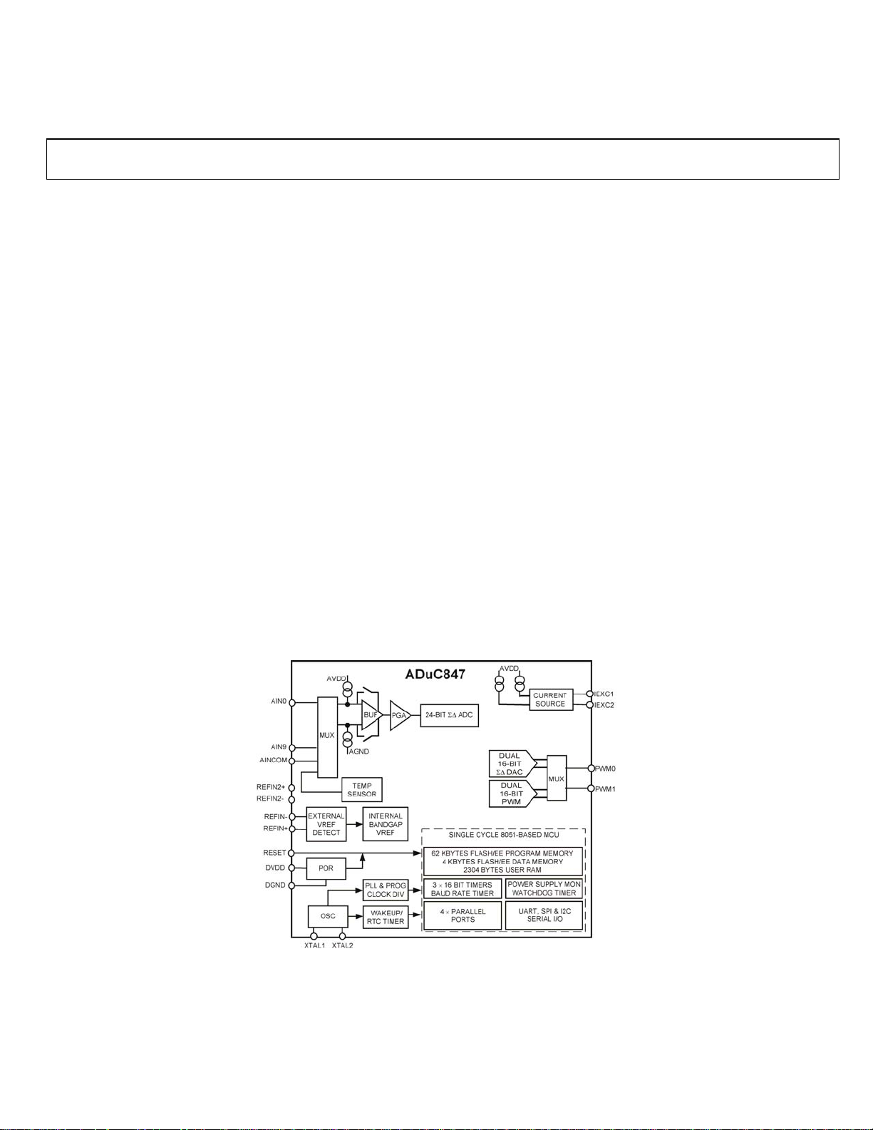
FUNCTIONAL BLOCK DIAGRAM
(Chop enabled)
On-Chip Peripherals
Internal Power on Reset Circuit
Dual 16-Bit S-D DACs/PWMs
On-Chip Temperature Sensor
Dual Excitation Current Sources
Time Interval Counter (Wakeup/RTC Timer)
UART, SPI®, and I2C® Serial I/O
High Speed Baud Rate Generator (incl 115,200)
Watchdog Timer (WDT)
Power Supply Monitor (PSM)
Power
Normal: 2.3mA Max @ 3.6 V (Core CLK = 1.57 MHz)
Power-Down: 20mA Max with Wakeup Timer Running
Specified for 3 V and 5 V Operation
Package and Temperature Range
52-Lead MQFP (14 mm x 14 mm), –40°C to +125°C
56-Lead CSP (8 mm x 8 mm), –40°C to +85°C
APPLICATIONS
Multi channel Sensor monitoring
Industrial/Environmental Instrumentation
WeighScales
Portable Instrumentation, Battery Powered Systems
4-20mA Transmitters
Data Logging
Precision System Monitoring
REV. PrA 05/03
Information furnished by Analog Devices is believed to be accurate and reliable. However, no
responsibility is assumed by Analog Devices for its use, nor for any infringements of patents or
other rights of third parties that may result from its use. No license is granted by implication or
otherwise under any patent or patent rights of Analog Devices. Trademarks and registered
trademarks are the property of their respective companies.
Purchase of licensed I2C components of Analog Devices or one of its sublicensed
Associated Companies conveys a license for the purchaser under the Philips I
Patent Rights to use these components in an I
conforms to the I
2
C Standard Specification as defined by Philips
2
C system, provided that the system
2
C
One Technology Way, P.O. Box 9106, Norwood, MA 02062-9106, U.S.A.
Tel: 781/329-4700 www.analog.com
Fax: 781/326-8703 © 2003 Analog Devices, Inc.
ll rights reserve
Page 2

Preliminary Technical Data ADuC847
SPECIFICATIONS
(AVDD = 2.7 V to 3.6 V or 4.75 V to 5.25 V, DVDD = 2.85 V to 3.6 V or 4.75 V to 5.25 V, REFIN(+) = 2.5 V, REFIN(–) = AGND; AGND = DGND = 0 V; XTAL1/XTAL2 = 32.768
kHz Crystal; all specifications T
PARAMETER MIN TYP MAX UNITS CONDITION
ADC (CHOP ENABLED) 1
Conversion Rate (Chop enabled) 5.4 19.79 105 Hz CHOP = 0 (ADCMODE.3)
(Chop disabled) 16.06 59.36 1365 Hz CHOP = 1 (ADCMODE.3)
No Missing Codes2 24 Bits 19.79Hz/ 59.36Hz Update Rate
Resolution (Chop enabled) 13.5 Bits Pk-Pk Range = ± 20mV, 20Hz Update Rate
(Chop disabled) 13 Bits Pk-Pk Range = ± 20mV, 59Hz Update Rate
(Chop enabled) 18.5 Bits Pk-Pk Range = ± 2.56V, 20Hz Update Rate
(Chop disabled) 17.4 Bits Pk-Pk Range = ± 2.56V, 59.4Hz Update Rate
Output Noise See Tables IV, V VI & VII in
Integral Non Linearity ±2 ± 15 ppm of FSR 1 LSB16
Offset Error3
See tables VI & VII
Offset Error Drift vs. Temp (Chop enabled) ± 10 nV/°C Chop Enabled
Offset Error Drift vs. Temp (Chop disabled) ±200 nV/°C Chop Disabled
Full-Scale Error4
Gain Error Drift vs. Temp 5
PARAMETER MIN TYP MAX UNITS CONDITION
ADC ANALOG INPUTS
Differential Input Voltage Ranges
Bipolar Mode (ADC0CON.5 = 0)
Unipolar Mode (ADC0CON.5 = 1) 0 Æ 1.024 x Vref/GAIN V V
ADC Range Matching ± 2
Power Supply Rejection 80 dBs AIN=1V, Range=± 2.56V
113 dBs AIN=7.8mV, Range=± 20mV
Common Mode DC Rejection
On AIN 95 dBs @DC, AIN=7.8mV, Range=± 20mV
On AIN 113 dBs @DC, AIN=1V, Range=± 2.56V
Common Mode 50/60Hz Rejection 20Hz Update Rate
On AIN 95 dBs 50/60Hz ± 1Hz, AIN=7.8mV, Range=± 20mV
On AIN 90 dBs 50/60Hz ± 1Hz, AIN=1V, Range=± 2.56V
59Hz Update Rate
On AIN 95 dBs 50/60Hz ± 1Hz, AIN=7.8mV, Range=± 20mV
On AIN 90 dBs 50/60Hz ± 1Hz, AIN=1V, Range=± 2.56V
Normal Mode 50/60 Hz Rejection
On AIN 60 dBs 50/60Hz ± 1Hz, 20Hz/59Hz Update Rate
Analog Input Current2
± 5 nA T
Analog Input Current Drift ± 5 pA/°C T
± 15 pA/°C T
AINCOM Input Current ± 125 nA/V ± 2.56V Range
AINCOM Input Current Drift ± 2 pA/V/°C
Absolute AIN Voltage Limits2
Absolute AINCOM Voltage Limits A
, to T
MIN
unless otherwise noted.). Buffer On unless otherwise noted.
MAX
± 0.5 ppm/°C
9, 10
A
GND
GND
Output Noise varies with selected Update Rates
ADC Description
± 3
µV
± 10
µV
± 1.024 x V
REF
/GAIN
V
µV
± 1 nA T
+ 0.1 AV
DD
– 0.1
V Ain0-Ain9 with Buffer ON
+ 0.03 AV
– 0.03 V Buffer bypassed (ADC0CON1.6=0,
DD
and Gain Range
CHOP Enabled
Offset Error is in the order of the noise for the
programmed gain and update rate following a
calibration for CHOP disabled.
V
= REFIN(+) - REFIN(-) (or Int 1.25V Ref)
REF
GAIN = 1 to 128
= REFIN(+) - REFIN(-) GAIN=1 to 128
REF
AIN=18mV
= 85°C
MAX
= 125°C
MAX
= 85°C
MAX
= 125°C
MAX
(ADC0CON1.6 = 0 & ADC0CON1.7 = 0)
ADC0CON1.7=1)
1
REV. PrA 05/03 2
Page 3

Preliminary Technical Data ADuC847
EXTERNAL REFERENCE INPUTS
REFIN(+) to REFIN(–) Range2
Average Reference Input Current 1
Average Reference Input Current Drift +/- 0.1 nA/V/°C
‘NO Ext. REF’ Trigger Voltage 0.3 0.65 V NOXREF bit active if VREF<0.3V
NOXREF bit Inactive if VREF>0.65
Common Mode DC Rejection 125 dBs @DC, AIN=1V, Range=± 2.56V
Common Mode 50/60Hz Rejection 90 dBs 50/60Hz ± 1Hz, AIN=1V, Range=± 2.56V
Normal Mode 50/60 Hz Rejection 60 dBs 50/60Hz ± 1Hz, 20Hz/59.4Hz Update Rate
PARAMETER MIN TYP MAX UNITS CONDITION
ADC SYSTEM CALIBRATION
Full Scale Calibration Limit +1.05 x FS V
Zero Scale Calibration Limit -1.05 x FS V
Input Span 0.8 x FS 2.1 x FS V
INT REFERENCE (CHOP ENABLED)
ADC Reference
Reference Voltage 1.237 1.25 1.2625 V initial tolerance @ 25°C, VDD=5V
Power Supply Rejection 45 dBs
Reference Tempco 100 ppm/°C
TEMPERATURE SENSOR
Accuracy +/- 2 °C
Thermal Impedance 90 °C/W MQFP Package
52 °C/W CSP Package
TRANSDUCER BURNOUT CURRENT SOURCES
AIN+ Current -100 nA AIN+ is the selected positive input (Ain4 or
AIN- Current 100 nA AIN- is the selected negative input (Ain5 or
Initial Tolerance at 25°C +/- 10 %
Drift 0.03 %/°C
EXCITATION CURRENT SOURCES
Output Current -200
Initial Tolerance at 25°C +/-10 %
Drift 200 ppm/°C
Initial Current Matching at 25°C +/-1 % Matching between both Current Sources
Drift Matching 20 ppm/°C
Line Regulation (AVDD) 1
Load Regulation 0.1 V
Output Compliance A
PARAMETER MIN TYP MAX UNITS CONDITION
POWER SUPPLY MONITOR (PSM)
AVDD Trip Point Selection Range 2.63 4.63 V Four Trip Points selectable in this range
AVDD Trip Point Accuracy +/- 3.0 % T
AVDD Trip Point Accuracy +/- 3.0 % T
DVDD Trip Point Selection Range 2.63 4.63 V Four Trip Points selectable in this range
DVDD Trip Point Accuracy +/- 3.0 % T
DVDD Trip Point Accuracy +/- 3.0 % T
1 2.5 AV
V
DD
µA/V
ADC Enabled
Ain6 only) to the ADC
Ain7 only) to the ADC
µA
µA/V
AVDD-0.6 V
GND
Available from each Current Source
AVDD=5V +/- 5%
MAX
MAX
MAX
MAX
= 85°C
= 125°C
= 85°C
= 125°C
REV. PrA 05/03 -3-
Page 4

Preliminary Technical Data ADuC847
CRYSTAL OSCILLATOR (XTAL 1AND XTAL2)
Logic Inputs, XTAL1 Only2
V
, Input Low Voltage 0.8 V DVDD = 5V
INL
0.4 V DVDD = 3V
V
, Input Low Voltage 3.5 V DVDD = 5V
INH
2.5 V DVDD = 3V
XTAL1 Input Capacitance 18 pF
XTAL2 Output Capacitance 18 pF
LOGIC INPUTS
All Inputs except SCLOCK, RESET
and XTAL1
V
2
, Input Low Voltage 0.8 V DVDD = 5V
INL
0.4 V DVDD = 3V
V
SCLOCK and RESET Only
(Schmidt Triggered Inputs)
, Input Low Voltage 2.0 V
INH
2
VT+ 1.3 3.0 V DVDD = 5V
0.95 2.5 V DVDD = 3V
VT- 0.8 1.4 V DVDD = 5V
0.4 1.1 V DVDD = 3V
VT+ - VT- 0.3 0.85 V DVDD = 5V or 3V
Input Currents 2.0 V
Port 0, P1.0ÆP1.7, EA
SCLOCK, MOSI,MISO SS13
+/-10
RESET +/-10
35 105
Port 2, Port 3 +/-10
-180 -660
-20 -75
Input Capacitance 10 pF All Digital Inputs
LOGIC OUTPUTS
All Digital Outputs except XTAL22
VOH, Output High Voltage 2.4 V
2.4 V
VOL, Output Low Voltage14 0.8 V I
0.8 V I
0.8 V I
Floating State Leakage Current +/-10
Floating State Output Capacitance 10 pF
PARAMETER MIN TYP MAX UNITS CONDITION
START UP TIME
At Power On 300 ms
After External RESET in Normal Mode 3 ms
After WDT RESET in Normal Mode 3 ms Controlled via WDCON SFR
From Idle Mode 10 us
From Power-Down Mode
Oscillator Running PLLCON.7 = 0
Wakeup with INT0 Interrupt 20 us
Wakeup with SPI Interrupt 20 us
Wakeup with TIC Interrupt 20 us
Wakeup with External RESET 3 us
Oscillator Powered Down PLLCON.7 = 1
Wakeup with INT0 Interrupt 20 us
Wakeup with SPI Interrupt 20 us
Wakeup with External RESET 5 ms
+/- 10
-10 -40
µA
µA
µA
µA
µA
µA
µA
µA
V
= 0V or VDD
IN
V
= 0V, DVDD=5V, Internal Pullup
IN
VIN = DVDD, DVDD=5V
VIN = 0V, DVDD=5V
VIN = DVDD, DVDD=5V, Internal Pull-Down
VIN = DVDD, DVDD=5V
VIN = 2V, DVDD=5V
VIN = 0.45V, DVDD=5V
DV
DD
DV
DD
= 8mA, SCLOCK, MOSI/SDATA
SINK
= 10mA, P1.0, P1.1
SINK
= 1.6mA, All Other Outputs
SINK
µA
= 5V, I
= 3V, I
SOURCE
SOURCE
= 80 µA
= 20 µA
REV. PrA 05/03 4
Page 5

Preliminary Technical Data ADuC847
FLAH/EE MEMORY RELIABILITY CHARACTERISTICS
Endurance16 100,000 700,000 Cycles
Data Retention17 100 Years
POWER REQUIREMENTS
Power Supply Voltages
AVDD 3V Nominal 2.85 3.6 V
AVDD 5V Nominal 4.75 5.25 V
DVDD 3V Nominal 2.85 3.6 V
DVDD 5V Nominal 4.75 5.25 V
5V POWER CONSUMPTION
Normal Mode
18, 19
DVDD Current 4 mA core clock = 1.57MHz
13 16 mA core clock = 12.58MHz
AVDD Current 180
Power-Down Mode
18, 19
DVDD Current 53
100
DVDD Current 30
80
AVDD Current 1
3
Typical Additional Peripheral Currents (AIDD and D IDD)
Primary ADC 1 mA
Auxiliary ADC 0.5 mA
Power Supply Monitor 50
DAC 150
Dual Excitation Current Sources 400
3V POWER CONSUMPTION
Normal Mode
18, 19
DVDD Current 2.3 mA core clock = 1.57MHz
8 10 mA core clock = 12.58MHz
AVDD Current 180
Power-Down Mode
18, 19
DVDD Current 20
40
DVDD Current 10
80
AVDD Current 1
3
NOTES
1 Temperature Range for ADuC847BS (MQFP package) is –40°C to +125°C.
Temperature Range for ADuC847BCP (CSP package) is –40°C to +85°C.
2 These numbers are not production tested but are guaranteed by design and/or characterization data on production release.
3 System Zero-Scale Calibration can remove this error.
4 The ADC is factory calibrated at 25°C with AVDD = DVDD = 5 V yielding this full-scale error of 10 µV. If user power supply or temperature conditions are
significantly different from these, an Internal Full-Scale Calibration will restore this error to 10 µV. A system zero-scale and full-scale calibration will remove
this error altogether.
5 Gain Error Drift is a span drift. To calculate Full-Scale Error Drift, add the Offset Error Drift to the Gain Error Drift times the full-scale input.
6 In general terms, the bipolar input voltage range to the ADC is given by RangeADC = ±(VREF 2
VREF = REFIN(+) to REFIN(–) voltage and VREF = 1.25 V when internal ADC VREF is selected.
RN = decimal equivalent of RN2, RN1, RN0
e.g., VREF = 2.5 V and RN2, RN1, RN0 = 1, 1, 0 the RangeADC = ±1.28 V, In unipolar mode, the effective range is 0 V to 1.28 V in our example.
7 1.25 V is used as the reference voltage to the ADC when internal VREF is selected via the XREF0 and XREF 1 bits in ADC0CON2.
8 The ADuC847BCP (CSP Package) has been qualified and tested with the base of the CSP Package floating.
9 Pins configured in SPI Mode, pins configured as digital inputs during this test.
10 Pins configured in I
11 Flash/EE Memory Reliability Characteristics apply to both the Flash/EE program memory and Flash/EE data memory.
2
C Mode only.
REV. PrA 05/03 -5-
4.75V < DVDD <5.25V, AVDD= 5.25V
µA
µA
µA
µA
µA
µA
µA
µA
µA
µA
T
= 85°C; Osc ON;TIC ON
MAX
T
= 125°C; Osc ON; TIC ON
MAX
T
= 85°C; Osc OFF
MAX
T
= 125°C; Osc OFF
MAX
T
= 85°C; Osc ON or OFF
MAX
T
= 125°C; Osc ON or OFF
MAX
4.75V < DVDD <5.25V, AVDD= 5.25V
µA
µA
µA
µA
µA
µA
µA
T
MAX
T
MAX
Osc OFF
T
MAX
T
MAX
T
MAX
RN
)/125, where:
= 85°C; Osc ON;TIC ON
= 125°C; Osc ON; TIC ON
= 125°C; Osc OFF
= 85°C; Osc ON or OFF
= 125°C; Osc ON or OFF
Page 6

Preliminary Technical Data ADuC847
12 Endurance is qualified to 100 Kcycles as per JEDEC Std. 22 method A117 and measured at –40 °C, +25°C, +85°C, and +125°C. Typical endurance at 25°C is
700 Kcycles.
13 Retention lifetime equivalent at junction temperature (TJ) = 55°C as per JEDEC Std. 22, Method A117. Retention lifetime based on an activation energy of
0.6eV will derate with junction temperature.
14 Power Supply current consumption is measured in Normal, Idle, and Power-Down Modes under the following conditions:
Normal Mode: Reset = 0.4 V, Digital I/O pins = open circuit, Core Clk changed via CD bits in PLLCON, Core Executing internal software loop.
Idle Mode: Reset = 0.4 V, Digital I/O pins = open circuit, Core Clk changed via CD bits in PLLCON, PCON.0 = 1, Core Execution suspended in idle mode.
Power-Down Mode: Reset = 0.4 V, All P0 pins and P1.2–P1.7 Pins = 0.4 V, All other digital I/O pins are open circuit, Core Clk changed via CD bits in
PLLCON, PCON.1 = 1, Core Execution suspended in power-down mode, OSC turned ON or OFF via OSC_PD bit (PLLCON.7) in PLLCON SFR.
15 DVDD power supply current will increase typically by 3 mA (3 V operation) and 10 mA (5 V operation) during a Flash/EE memory program or erase cycle.
Specifications subject to change without notice
REV. PrA 05/03 6
Page 7
Preliminary Technical Data ADuC847
ABSOLUTE MAXIMUM RATINGS1
(TA = 25°C unless otherwise noted)
AVDD to AGND –0.3 V to +7 V
AVDD to DGND –0.3 V to +7 V
DVDD to AGND –0.3 V to +7 V
DVDD to DGND –0.3 V to +7 V
AGND to DGND
AVDD to DVDD –2 V to +5 V
Analog Input Voltage to AGND
Reference Input Voltage to AGND –0.3 V to AVDD +0.3 V
AIN/REFIN Current (Indefinite) 30 mA
Digital Input Voltage to DGND –0.3 V to DVDD +0.3 V
Digital Output Voltage to DGND –0.3 V to DVDD +0.3 V
Operating Temperature Range –40°C to +125°C
Storage Temperature Range –65°C to +150°C
Junction Temperature 150°C
qJA Thermal Impedance 90°C/W
Lead Temperature, Soldering Vapor Phase (60 sec) 215°C
Infrared (15 sec) 220°C
1
Stresses above those listed under Absolute Maximum Ratings may cause
permanent damage to the device. This is a stress rating only; functional operation
of the device at these or any other conditions above those listed in the operational
sections of this specification is not implied. Exposure to absolute maximum
rating conditions for extended periods may affect device reliability.
2
AGND and DGND are shorted internally on the ADuC847.
3
Applies to P1.0 to P1.7 pins operating in analog or digital input modes
2
–0.3 V to +0.3 V
3
–0.3 V to AV
DD
+0.3 V
.
REV. PrA 05/03 -7-
Page 8

Preliminary Technical Data ADuC847
ORDERING GUIDE
MODEL Temperature Range Package Description Package Option
ADuC847BS62-5
ADuC847BS62-3
ADuC847BCP62-5
ADuC847BCP62-3
ADuC847BCP32-5
ADuC847BCP32-3
ADuC847BCP8-5
ADuC847BCP8-3
EVAL-ADuC847QS
EVAL-ADuC847QSP
CAUTION
ESD (electrostatic discharge) sensitive device. Electrostatic charges as high as 4000 V
readily accumulate on the human body and test equipment and can discharge without
detection. Although the ADuC847 features proprietary ESD protection circuitry,
permanent damage may occur on devices subjected to high-energy electrostatic
discharges. Therefore, proper ESD precautions are recommended to avoid performance
degradation or loss of functionality.
-40 Æ +125oC 52-Lead Plastic Quad Flatpack, 62kB, 5v S-52
-40 Æ +125oC 52-Lead Plastic Quad Flatpack, 62kB, 3v S-52
-40 Æ +85
-40 Æ +85oC 56-Lead Chip Scale Package, 62kB, 3v CP-56
-40 Æ +85oC 56-Lead Chip Scale Package, 32kB, 5v CP-56
-40 Æ +85oC 56-Lead Chip Scale Package, 32kB, 3v CP-56
-40 Æ +85
-40 Æ +85
o
C 56-Lead Chip Scale Package, 62kB, 5v CP-56
o
C 56-Lead Chip Scale Package, 8kB, 5v CP-56
o
C 56-Lead Chip Scale Package, 8kB, 3v CP-56
QuickStartTM Development System
QuickStart PLUS Development System
REV. PrA 05/03 8
Page 9

Preliminary Technical Data ADuC847
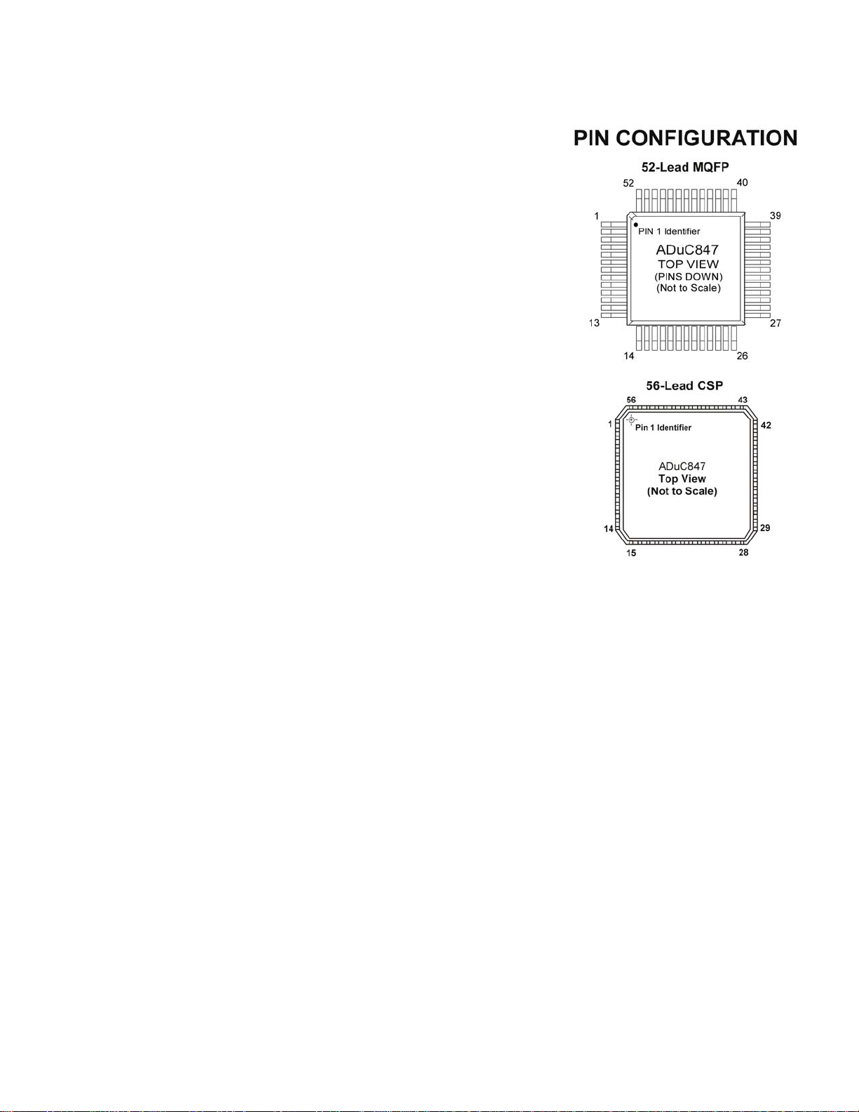
PIN FUNCTION DESCRIPTIONS
Pin No:
52-MQFP
1 56 P1.0/AIN0 I By power on default P1.0/AIN0 is configured as the AIN0 Analog Input.
2 1 P1.1/AIN1 I By power on default P1.1/AIN1 is configured as the AIN1 Analog Input.
3 2 P1.2/AIN2/REFIN2+ I By power on default P1.2/AIN2 is configured as the AIN2 Analog Input.
4 3 P1.3/AIN3/REFIN2- I By power on default P1.3/AIN3 is configured as the AIN3 Analog Input.
5 4 AVDD S Analog Supply Voltage
6 5 AGND S Analog Ground.
--- 6 AGND S A second Analog ground is provided with the CSP version only*
7 7 REFIN- I External Differential Reference Input, negative terminal
8 8 REFIN+ I External Differential Reference Input, positive terminal
9 9 P1.4/AIN4 I By power on default P1.4/AIN4 is configured as the AIN4 Analog Input.
10 10 P1.5/AIN5 I By power on default P1.5/AIN5 is configured as the AIN5 Analog Input.
11 11 P1.6/AIN6/IEXC1 I/O By power on default P1.6/AIN6 is configured as the AIN6 Analog Input.
*Note: This pin is provided on the CSP version only.
Pin No:
56-CSP
Pin
Mnemonic
Type* Description
AIN0 can be used as a pseudo differential input when used with AINCOM or
as the positive input of a fully differential pair when used with AIN2.
P1.0 has no digital output driver. It can function as a digital input for which
‘0’ must be written to the port bit. As a digital input, this pin must be driven
high or low externally.
AIN1 can be used as a pseudo differential input when used with AINCOM or
as the negative input of a fully differential pair when used with AIN0.
P1.1 has no digital output driver. It can function as a digital input for which
‘0’ must be written to the port bit. As a digital input, this pin must be driven
high or low externally.
AIN2 can be used as a pseudo differential input when used with AINCOM or
as the positive input of a fully differential pair when used with AIN3.
P1.2 has no digital output driver. It can function as a digital input for which
‘0’ must be written to the port bit. As a digital input, this pin must be driven
high or low externally. This pin also functions as a second external
differential reference input, positive terminal.
AIN3 can be used as a pseudo differential input when used with AINCOM or
as the negative input of a fully differential pair when used with AIN2.
P1.3 has no digital output driver. It can function as a digital input for which
‘0’ must be written to the port bit. As a digital input, this pin must be driven
high or low externally. This pin also functions as a second external
differential reference input, negative terminal.
AIN4 can be used as a pseudo differential input when used with AINCOM or
as the positive input of a fully differential pair when used with AIN5.
P1.0 has no digital output driver. It can function as a digital input for which
‘0’ must be written to the port bit. As a digital input, this pin must be driven
high or low externally.
AIN5 can be used as a pseudo differential input when used with AINCOM or
as the negative input of a fully differential pair when used with AIN4.
P1.1 has no digital output driver. It can function as a digital input for which
‘0’ must be written to the port bit. As a digital input, this pin must be driven
high or low externally.
AIN6 can be used as a pseudo differential input when used with AINCOM or
as the positive input of a fully differential pair when used with AIN7.
One or Both current sources can also be configured at this pin.
P1.0 has no digital output driver. It can function as a digital input for which
‘0’ must be written to the port bit. As a digital input, this pin must be driven
high or low externally.
REV. PrA 05/03 -9-
Page 10

Preliminary Technical Data ADuC847
Pin No:
52-MQFP
12 12 P1.7/AIN7/IEXC2 I/O By power on default P1.7/AIN7 is configured as the AIN7 Analog Input. AIN7
13 13 AINCOM I All analog inputs can be referred to this pin provided a relevant pseudo
14 14 ---- ----
---- 15 AIN8 I AIN8 can be used as a pseudo differential analog input when used with
---- 16 AIN9 I AIN9 can be used as a pseudo differential analog input when used with
15 17 RESET I Reset Input. A high level on this pin for 16 core clock cycles while the
16-19
22-25
16
17
18
19
22
23
24
25
20, 34, 48 22, 36, 51 DVDD S Digital Supply Voltage
21, 35, 47 23, 37, 38,
26 28 SCLK (I2C) I/O Serial interface clock for the I2C interface. As an input this pin is a Schmitt
27 29 SDATA I/O Serial data pin for the I2C interface. As an input this pin has a weak internal
*Note: This pin is provided on the CSP version only.
Pin No:
56-CSP
18-21
24-27
18
19
20
21
24
25
26
27
50
Pin
Mnemonic
P3.0 Æ P3.7
P3.0/RXD
P3.1/TXD
P3.2/INT0
P3.3/INT1
P3.4/T0
P3.5/T1
P3.6//WR
P3.7//RD
DGND S Digital Ground.
Type* Description
can be used as a pseudo differential input when used with AINCOM or as the
negative input of a fully differential pair when used with AIN6.
One or Both current sources can also be configured at this pin
P1.1 has no digital output driver. It can function as a digital input for which ‘0’
must be written to the port bit. As a digital input, this pin must be driven high
or low externally.
differential input mode is selected.
AINCOM or as the positive input of a fully differential pair when used with
AIN9*.
AINCOM or as the negative input of a fully differential pair when used with
AIN8*.
oscillator is running resets the device. There is an internal weak pull-down and
a Schmitt trigger input stage on this pin.
I/O P3.0–P3.7 are bi-directional port pins with internal pull-up resistors. Port 3 pins
that have 1s written to them are pulled high by the internal pull-up resistors,
and in that state can be used as inputs. As inputs, Port 3 pins being pulled
externally low will source current because of the internal pull-up resistors.
When driving a 0-to-1 output transition, a strong pull-up is active for two core
clock periods of the instruction cycle.
Port 3 pins also have various secondary functions described below.
Receiver Data for UART serial Port
Transmitter Data for UART serial Port
External Interrupt 0. This pin can also be used as a gate control input to
Timer0.
External Interrupt 1. This pin can also be used as a gate control input to
Timer1.
Timer/Counter 0 External Input
Timer/Counter 1 External Input
External Data Memory Write Strobe. Latches the data byte from Port 0 into an
external data memory.
External Data Memory Read Strobe. Enables the data from an external data
memory to Port 0.
triggered input and a weak internal pull-up is present on this pin unless it is
outputting logic low. this pin can also be controlled in software as a digital
output pin.
pull-up present unless it is outputting logic low.
REV. PrA 05/03 10
Page 11

Preliminary Technical Data ADuC847
Pin No:
52-MQFP
28 Æ 31
36 Æ 39
28
29
30
31
36
37
38
39
32 34 XTAL1
33 35 XTAL2
40 43 EA
41 44 PSEN
42 45 ALE
Pin No:
56-CSP
30 Æ 33
39 Æ 42
30
31
32
33
39
40
41
42
Pin
Mnemonic
P2.0 Æ P2.7
P2.0/SCLOCK
(SPI)
P2.1/MOSI
P2.2/MISO
P2.3/SS/T2
P2.4/T2EX
P2.5/PWM0
P2.6/PWM1
P2.7/PWMCLK
Type* Description
I/O Port 2 is a bidirectional port with internal pull-up resistors. Port 2 pins that
have 1s written to them are pulled high by the internal pull-up resistors, and in
that state can be used as inputs. As inputs, Port 2 pins being pulled externally
low will source current because of the internal pull-up resistors. Port 2 emits
the middle and high order address bytes during accesses to the 24-bit external
data memory space.
Port 2 pins also have various secondary functions described below.
Serial interface clock for the SPI interface. As an input this pin is a Schmitt
triggered input and a weak internal pull-up is present on this pin unless it is
outputting logic low.
Serial master output/slave input data for the SPI interface. A strong internal
pull-up is present on this pin when the SPI interface outputs a logic high. A
strong internal pull-down is present on this pin when the SPI interface outputs
a logic low.
Master Input/Slave Output for the SPI Interface. There is a weak pull-up on
this input pin.
Slave select input for the SPI Interface is present at this pin. A weak pull-up is
present on this pin.
On both package options this pin can also be used to provide a clock input to
Timer 2. When Enabled, counter 2 is incremented in response to a negative
transition on the T2 input pin.
This pin can be used to provide a control input to Timer 2. When Enabled, a
negative transition on the T2EX input pin will cause a Timer 2 capture or
reload event.
If the PWM is enabled then the PWM0 output will appear at this pin.
If the PWM is enabled then the PWM1 output will appear at this pin.
If the PWM is enabled then an external PWM clock can be provided at this
pin.
I Input to the crystal oscillator inverter.
O Output from the crystal oscillator inverter. (see “Hardware Design
Considerations” for description)
External Access Enable, Logic Input. When held high, this input enables the
device to fetch code from internal program memory locations 0000h to F7FFh.
No external program memory access is available on the ADuC847. To
determine the mode of code execution, the EA pin is sampled at the end of an
external RESET assertion or as part of a device power cycle.
EA may also be used as an external emulation I/O pin and therefore the
voltage level at this pin must not be changed during normal mode operation as
it may cause an emulation interrupt that will halt code execution.
Program Store Enable, Logic Output. It is active every six oscillator periods
except during external data memory accesses. This pin remains high during
internal program execution.
PSEN can also be used to enable serial download mode when pulled low
through a resistor at the end of an external RESET assertion or as part of a
device power cycle.
Address Latch Enable, Logic Output. This output is used to latch the low byte
(and page byte for 24-bit data address space accesses) of the address to
external memory during external data memory access cycles. It is activated
every six oscillator periods except during an external data memory access. It
can be disabled by setting the PCON.4 bit in the PCON SFR.
REV. PrA 05/03 -11-
Page 12

Preliminary Technical Data ADuC847
Pin No:
52-MQFP
43 Æ 46
49 Æ 52
*I = Input, O = Output, S = Supply.
Pin numbers subject to change.
Pin No:
56-CSP
46 Æ 49
52 Æ 55
Pin
Mnemonic
P0.0 Æ P0.7 I/O P0.0–P0.7, these pins are part of Port0 which is an 8-bit open-drain
DETAILED BLOCK DIAGRAM WITH PIN NUMBERS
Type* Description
bidirectional I/O port. Port 0 pins that have 1s written to them float and in that
state can be used as high impedance inputs. An external pull-up resistor will
be required on P0 outputs to force a valid logic high level externally. Port 0 is
also the multiplexed low-order address and data bus during accesses to
external data memory. In this application it uses strong internal pull-ups when
emitting 1s.
Pin numbers refer to the 52pin MQFP package.
Figure 1: Detailed Block Diagram of the ADuC847
REV. PrA 05/03 12
Page 13

Preliminary Technical Data ADuC847
COMPLETE SFR MAP
Figure 2 below shows a full SFR memory map and the SFR contents af te r RESET. NOT USED indicates unoccupied SFR locations. Un o c cupied locations
in the SFR address space are not implemented; i.e., no register exists at this location. If an unoccupied location is read, an unspecified value is
returned. SFR locations that are reserved for future use are shaded (RESERVED) and should not be accessed by user software.
Figure 2: Complete SFR Map
REV. PrA 05/03 -13-
Page 14

Preliminary Technical Data ADuC847
INTRODUCTION
The ADuC847 is a 12.58MIPs 8052 core upgrade to the ADuC834
and is very similar to the ADuC845. It includes additional analog
inputs for applications requiring more ADC channels as does the
ADuC845 but removes the DAC and Auxiliary ADC from the
ADuC845 specification. Otherwise it has all the same features as
the ADuC834, but the standard 12-cycle 8052 core has been
replaced with a 12.58MIPs single cycle core.
Since the ADuC847 and ADuC834 share the same feature set only
the differences between the two chips are documented here. For full
documentation on the ADuC834 please consult the datasheet
available at
GENERAL DESCRIPTION
The ADuC847 is a complete smart transducer front end,
integrating a high resolution sigma-delta ADC with flexible,
10/8-channel input multiplexing, a fast 8-bit MCU, and
program/data Flash/EE memory on a single chip.
The ADC includes flexible input multiplexing, a temperature
sensor and a PGA (allowing direct measurement of low level
signals). The ADC, with on-chip digital filtering and
programmable output data rates is intended for the measurement
of wide dynamic range, low frequency signals, such as those in
weigh scale, strain-gage, pressure transducer, or temperature
measurement applications.
The device operates from a 32 kHz crystal with an on-chip PLL
generating a high frequency clock of 12.58 MHz. This clock is
routed through a programmable clock divider from which the
MCU core clock operating frequency is generated. The
microcontroller core is an optimized single cycle 8052 offering
up to 12.58MIPs performance while maintaining the 8051
instruction set compatibility.
62 Kbytes of nonvolatile Flash/EE program memory, 4 Kbytes
of nonvolatile Flash/EE data memory, and 2304 bytes of data
RAM are provided on-chip. The program memory can be
configured as data memory to give up to 60 Kbytes of NV data
memory in data logging applications.
On-chip factory firmware supports in-circuit serial download and
debug modes (via UART), as well as single-pin emulation mode
via the EA pin. The ADuC847 is supported by a QuickStart™
development system featuring low cost software and hardware
development tools
8052 Instruction Set
The following pages document the number of clock cycles required
for each instruction. Most instructions are executed in one or two
clock cycles resulting in 12.6MIPs peak performance when
operating at PLLCON = 00H.
Timer Operation
Timers on a standard 8052 increment by one with each machine
cycle. On the ADuC847 one machine cycle is equal to one clock
cycle hence the timers will increment at the same rate as the core
clock.
http://www.analog.com/microconverter
ALE
The output on the ALE pin on the ADuC834 was a clock at 1/6th of
the core operating frequency. On the ADuC847 the ALE pin
operates as follows….
For a single machine cycle instruction: ALE is high for the first
half of the machine cycle and low for the second half. The ALE
output is at the core operating frequency. For a two or more
machine cycle instruction: ALE is high for the first half of the first
machine cycle and then low for the rest of the machine cycles.
External Memory Access
There is no support for external program memory access on the
ADuC847. When accessing external RAM the EWAIT register
may need to be programmed in order to give extra machine cycles
to MOVX commands. This is to account for differing external
RAM access speeds.
REV. PrA 05/03 14
Page 15

Preliminary Technical Data ADuC847
INSTRUCTION TABLE
Optimized Single Cycle 8051 Instruction Set
Mnemonic Description Bytes Cycles
Arithmetic
ADD A,Rn Add register to A 1 1
ADD A,@Ri Add indirect memory to A 1 2
ADD A,dir Add direct byte to A 2 2
ADD A,#data Add immediate to A 2 2
ADDC A,Rn Add register to A with carry 1 1
ADDC A,@Ri Add indirect memory to A with carry 1 2
ADDC A,dir Add direct byte to A with carray 2 2
ADD A,#data Add immediate to A with carry 2 2
SUBB A,Rn Subtract register from A with borrow 1 1
SUBB A,@Ri Subtract indirect memory from A with borrow 1 2
SUBB A,dir Subtract direct from A with borrow 2 2
SUBB A,#data Subtract immediate from A with borrow 2 2
INC A Increment A 1 1
INC Rn Increment register 1 1
INC @Ri Increment indirect memory 1 2
INC dir Increment direct byte 2 2
INC DPTR Increment data pointer 1 3
DEC A Decrement A 1 1
DEC Rn Decrement Register 1 1
DEC @Ri Decrement indirect memory 1 2
DEC dir Decrement direct byte 2 2
MUL AB Multiply A by B 1 9
DIV AB Divide A by B 1 9
DA A Decimal Adjust A 1 2
Logic
ANL A,Rn AND register to A 1 1
ANL A,@Ri AND indirect memory to A 1 2
ANL A,dir AND direct byte to A 2 2
ANL A,#data AND immediate to A 2 2
ANL dir,A AND A to direct byte 2 2
ANL dir,#data AND immediate data to direct byte 3 3
ORL A,Rn OR register to A 1 1
ORL A,@Ri OR indirect memory to A 1 2
ORL A,dir OR direct byte to A 2 2
ORL A,#data OR immediate to A 2 2
ORL dir,A OR A to direct byte 2 2
ORL dir,#data OR immediate data to direct byte 3 3
XRL A,Rn Exclusive-OR register to A 1 1
XRL A,@Ri Exclusive-OR indirect memory to A 2 2
XRL A,#data Exclusive-OR immediate to A 2 2
XRL dir,A Exclusive-OR A to direct byte 2 2
XRL A,dir Exclusive-OR indirect memory to A 2 2
XRL dir,#data Exclusive-OR immediate data to direct 3 3
CLR A Clear A 1 1
CPL A Complement A 1 1
SWAP A Swap Nibbles of A 1 1
RL A Rotate A left 1 1
RLC A Rotate A left through carry 1 1
RR A Rotate A right 1 1
RRC A Rotate A right through carry 1 1
Data Transfer
MOV A,Rn Move register to A 1 1
MOV A,@Ri Move indirect memory to A 1 2
MOV Rn,A Move A to register 1 1
MOV @Ri,A Move A to indirect memory 1 2
MOV A,dir Move direct byte to A 2 2
MOV A,#data Move immediate to A 2 2
MOV Rn,#data Move register to immediate 2 2
REV. PrA 05/03 -15-
Page 16

Preliminary Technical Data ADuC847
Mnemonic Description Bytes Cycles
MOV dir,A Move A to direct byte 2 2
MOV Rn, dir Mov register to direct byte 2 2
MOV dir, Rn Move direct to register 2 2
MOV @Ri,#data
MOV dir,@Ri
MOV @Ri,dir
MOV dir,dir Move direct byte to direct byte 3 3
MOV dir,#data Move immediate to direct byte 3 3
MOV DPTR,#data Move immediate to data pointer 3 3
MOVC A,@A+DPTR Move code byte relative DPTR to A 1 4
MOVC A,@A+PC Move code byte relative PC to A 1 4
MOVX A,@Ri Move external (A8) data to A 1 4
MOVX A,@DPTR Move external (A16) data to A 1 4
MOVX @Ri,A Move A to external data (A8) 1 4
MOVX @DPTR,A Move A to external data (A16) 1 4
PUSH dir Push direct byte onto stack 2 2
POP dir Pop direct byte from stack 2 2
XCH A,Rn Exchange A and register 1 1
XCH A,@Ri Exchange A and indirect memory 1 2
XCHD A,@Ri Exchange A and indirect memory nibble 1 2
XCH A,dir Exchange A and direct byte 2 2
Boolean
CLR C Clear carry 1 1
CLR bit Clear direct bit 2 2
SETB C Set Carry 1 1
SETB bit Set direct bit 2 2
CPL C Complement carry 1 1
CPL bit Complement direct bit 2 2
ANL C,bit AND direct bit and carry 2 2
ANL C,/bit AND direct bit inverse to carry 2 2
ORL C,bit OR direct bit and carry 2 2
ORL C,/bit OR direct bit inverse to carry 2 2
MOV C,bit Move direct bit to carry 2 2
MOV bit,C Move carry to direct bit 2 2
Branching
JMP @A+DPTR Jump indirect relative to DPTR 1 3
RET Return from subroutine 1 4
RETI Return from interrupt 1 4
ACALL addr11 Absolute jump to subroutine 2 3
AJMP addr11 Absolute jump unconditional 2 3
SJMP rel Short jump (relative address) 2 3
JC rel Jump on carry = 1 2 3
JNC rel Jump on carry = 0 2 3
JZ rel Jump on accumulator = 0 2 3
JNZ rel Jump on accumulator ! = 0 2 3
DJNZ Rn,rel Decrement register, jnz relative 2 3
LJMP Long jump unconditional 3 4
LCALL addr16 Long jump to subroutine 3 4
JB bit,rel Jump on direct bit = 1 3 4
JNB bit,rel Jump on direct bit = 0 3 4
JBC bit,rel Jump on direct bit = 1 and clear 3 4
CJNE A,dir,rel Compare A, direct JNE relative 3 4
CJNE A,#data,rel Compare A, immediate JNE relative 3 4
CJNE Rn,#data,rel Compare register, immediate JNE relative 3 4
CJNE @Ri,#data,rel Compare indirect, immediate JNE relative 3 4
DJNZ dir,rel Decrement direct byte, JNZ relative 3 4
Miscellaneous
NOP No operation 1 1
1. One cycle is one clock.
2. MOVX instructions are four cycles when they have 0 wait state. Cycles of MOVX instructions are 4 + n cycles when they have n wait states.
3. LCALL instruction are three cycles when the LCALL instruction comes from an interrupt.
Move immediate to indirect memory
Move indirect to direct memory
Move direct to indirect memory
2
2
2
REV. PrA 05/03 16
2
2
2
Page 17

Preliminary Technical Data ADuC847
MEMORY7 ORGANISATION
The ADuC847 contains 4 different memory blocks namely:
- 62k/30k/6k Bytes of On-Chip Flash/EE Program Memory
- 4kBytes of On-Chip Flash/EE Data Memory
- 256 Bytes of General Purpose RAM
- 2kBytes of Internal XRAM
(1) Flash/EE Program Memory
The ADuC847 provides up to 62kBytes of Flash/EE program
memory to run user code.
When EA is pulled high externally during a power cycle or a
hardware reset the part defaults to code execution from its internal
62kBytes of Flash/EE program memory. The ADuC847 does not
support the rollover from internal code space to external code
space. No external code space is available on the ADuC847.
Permanently embedded firmware allows code to be serially
downloaded to the 62kBytes of internal code space via the UART
serial port while the device is in-circuit. No external hardware is
required.
56kBytes of the program memory can be reprogrammed during
runtime hence the code space can be upgraded in the field using a
user defined protocol or it can be used as a data memory. This will
be discussed in more detail in the Flash/EE Memory section of the
datasheet.
(2) Flash/EE Data Memory
4kBytes of Flash/EE Data Memory are available to the user and
can be accessed indirectly via a group of registers mapped into the
Special Function Register (SFR) area. Access to the Flash/EE Data
memory is discussed in detail later as part of the Flash/EE memory
section in this data sheet.
(3) General Purpose RAM
The general purpose RAM is divided into two separate memories,
namely the upper and the lower 128 bytes of RAM. The lower 128
bytes of RAM can be accessed through direct or indirect addressing
while the upper 128 bytes of RAM can only be accessed through
indirect addressing as it shares the same address space as the SFR
space which can only be accessed through direct addressing.
The lower 128 bytes of internal data memory are mapped as shown
in Figure 3. The lowest 32 bytes are grouped into four banks of
eight registers addressed as R0 through R7. The next 16 bytes (128
bits), locations 20Hex through 2FHex above the register banks,
form a block of directly addressable bit locations at bit addresses
00H through 7FH. The stack can be located anywhere in the
internal memory address space, and the stack depth can be
expanded up to 2048 bytes.
Reset initializes the stack pointer to location 07 hex. Any call or
push pre-increments the SP before loading the stack. Hence
loading the stack starts from locations 08 hex which is also the first
register (R0) of register bank 1. Thus, if one is going to use more
than one register bank, the stack pointer should be initialized to an
area of RAM not used for data storage.
REV. PrA 05/03 -17-
30H
BANKS
SELECTED
VIA
BITS IN PSW
20H
11
18H
10
10H
01
08H
00
00H
Figure 3. Lower 128 Bytes of Internal Data Memory
(4) Internal XRAM
The ADuC847 contains 2kBytes of on-chip extended data memory.
This memory, although on-chip, is accessed via the MOVX
instruction. The 2kBytes of internal XRAM are mapped into the
bottom 2kBytes of the external address space if the CFG847.0 (see
Table III) bit is set, otherwise access to the external data memory
will occur just like a standard 8051.
Even with the CFG847.0 bit set access to the external XRAM will
occur once the 24 bit DPTR is greater than 0007FFH.
Figure 4: Internal and External XRAM
When accessing the internal XRAM, the P0, P2 port pins as well as
the RD and WR strobes will not be output as per a standard 8051
MOVX instruction. This allows the user to use these port pins as
standard I/O.
7FH
GENERAL-PURPOSE
AREA
2FH
BIT-ADDRESSABLE
(BIT ADDRESSES)
1FH
17H
FOUR BANKS OF EIGHT
REGISTERS
0FH
R0 R7
07H
RESET VALUE OF
STACK POINTER
Page 18

Preliminary Technical Data ADuC847
The upper 1792 bytes of the internal XRAM can be configured to
be used as an extended 11-bit stack pointer. By default the stack
will operate exactly like an 8052 in that it will rollover from FFh to
00h in the general purpose RAM. On the ADuC847 however it is
possible (by setting CFG847.7) to enable the 11-bit extended stack
pointer. In this case the stack will rollover from FFh in RAM to
0100h in XRAM.
The 11-bit stack pointer is visable in the SP and SPH SFRs. The SP
SFR is located at 81h as with a standard 8052. The SPH SFR is
located at B7h. The 3 LSBs of this SFR contain the 3 extra bits
necessary to extend the 8-bit stack pointer into an 11-bit stack
pointer.
07FFH
UPPER 1792
BYTES OF
ON-CHIP XRAM
(DATA +STACK
FOR EXSP=1,
DATA ONLY
100H
00H
FOR EXSP=0)
LOWER 25 6
BYTES OF
ON-CHIP XRAM
(DATA ONLY)
CFG845.7 = 0
FFH
256 BYTES OF
ON-CHIP DATA
(DATA + STACK)
00H
CFG845.7 = 1
RAM
Figure 4. Extended Stack Pointer Operation
External Data Memory (External XRAM)
Just like a standard 8051 compatible core the ADuC847 can access
external data memory using a MOVX instruction. The MOVX
instruction automatically outputs the various control strobes
required to access the data memory.
The ADuC847 however, can access up to 16MBytes of external
data memory. This is an enhancement of the 64kBytes external data
memory space available on a standard 8051 compatible core.
The external data memory is discussed in
more detail in the ADuC847 Hardware
Design Considerations section.
SPECIAL FUNCTION REGISTERS
(SFRs)
internal data memory space and accessed by direct addressing only.
It provides an interface between the CPU and all on chip
peripherals. A block diagram showing the programming model of
the ADuC847 via the SFR area is shown in Figure 5. All registers
except the Program Counter (PC) and the four general-purpose
register banks, reside in the SFR area. The SFR registers include
control, configuration, and data registers that provide an interface
between the CPU and all on-chip peripherals.
The SFR space is mapped into the upper 128 bytes of
Figure 5. Programming Model
Accumulator SFR (ACC)
ACC is the Accumulator register and is used for math operations
including addition, subtraction, integer multiplication and division,
and Boolean bit manipulations. The mnemonics for accumulatorspecific instructions refer to the Accumulator as A.
B SFR (B)
The B register is used with the ACC for multiplication and division
operations. For other instructions it can be treated as a generalpurpose scratchpad register.
Data Pointer (DPTR)
The Data Pointer is made up of three 8-bit registers, named DPP
(page byte), DPH (high byte) and DPL (low byte). These are used
to provide memory addresses for internal and external code access
and external data access. It may be manipulated as a 16-bit register
(DPTR = DPH, DPL), although INC DPTR instructions will
automatically carry over to DPP, or as three independent 8-bit
registers (DPP, DPH, DPL).
The ADuC847 supports dual data pointers. Refer to the Dual Data
Pointer section later in this datasheet.
Stack Pointer (SP and SPH)
The SP SFR is the stack pointer and is used to hold an internal
RAM address that is called the ‘top of the stack.’ The SP register is
incremented before data is stored during PUSH and CALL
executions. While the Stack may reside anywhere in on-chip RAM,
the SP register is initialized to 07H after a reset. This causes the
stack to begin at location 08H.
As mentioned earlier the ADuC847 offers an extended 11-bit stack
pointer. The 3 extra bits to make up the 11-bit stack pointer are the
3 LSBs of the SPH byte located at B7h. To enable the SPH SFR the
EXSP (CFG847.7) bit must be set otherwise the SPH SFR cannot
be read or written to.
REV. PrA 05/03 18
Page 19

Preliminary Technical Data ADuC847
Program Status Word (PSW)
The PSW SFR contains several bits reflecting the current status of
the CPU as detailed in Table I.
SFR Address D0H
Power ON Default Value 00H
Bit Addressable Yes
Table I. PSW SFR Bit Designations
Bit Name Description
7 CY Carry Flag
6 AC Auxiliary Carry Flag
5 F0 General-Purpose Flag
4 RS1 Register Bank Select Bits
3 RS0
2 OV Overflow Flag
1 F1 General-Purpose Flag
0 P Parity Bit
Power Control Register (PCON)
The PCON SFR contains bits for power-saving options and
general-purpose status flags as shown in Table II.
SFR Address 87H
Power ON Default Value 00H
Bit Addressable No
Table II. PCON SFR Bit Designations Bit Name Description
7 SMOD Double UART Baud Rate
6 SERIPD SPI Power-Down Interrupt
5 INT0PD INT0 Power-Down Interrupt
4 ALEOFF Disable ALE Output
3 GF1 General-Purpose Flag Bit
2 GF0 General-Purpose Flag Bit
1 PD Power-Down Mode Enable
0 IDL Idle Mode Enable
RS1 RS0 Selected Bank
0 0 0
0 1 1
1 0 2
1 1 3
Enable
Enable
847 Configuration Register (CFG847)
The CFG847 SFR contains the necessary bits to configure the
internal XRAM and the extended SP. By default it configures the
user into 8051 mode. i.e. extended SP is disabled, internal XRAM
is disabled.
SFR Address AFhH
Power ON Default Value 00H
Bit Addressable No
Table III. CFG847 SFR Bit Designations
Bit Name Description
7 EXSP Extended SP Enable.
If this bit is set to 1 then the stack will
rollover from SPH/SP = 00FFh to
0100h.
If this bit is cleared to 0 then the SPH
SFR will be disabled and the stack will rollover
from SP=FFh to SP =00h
6 ---5 ---4 ---3 ---2 ---1 ---0 XRAMEN XRAM Enable Bit
----
----
----
----
----
----
If this bit is set to 1 then the internal XRAM
will be mapped into the lower 2kBytes of the
external address space. If this bit is cleared to 0
then the internal XRAM will not be accessible
and the external data memory will be mapped
into the lower 2kBytes of external data
memory. (see figure 4).
REV. PrA 05/03 -19-
Page 20

Preliminary Technical Data ADuC847
ADC CIRCUIT INFORMATION
The ADuC847 incorporates a 10-channel (8-channel on the MQFP
package) 24-bit Σ−∆ ADC. It also includes an on-chip
programmable gain amplifier and digital filtering intended for the
measurement of wide dynamic range, low frequency signals such
as those in weigh-scale, strain-gauge, pressure transducer, or
temperature measurement applications.
The ADuC847 can be configured as four/five fully-differential
input channels or as eight/ten pseudo-differential input channels
referenced to AINCOM. The ADC is buffered and can be
programmed for one of eight input ranges from ±20 mV to ±2.56V.
Buffering the input channel means that the part can handle
significant source impedances on the analog input and that R,C
filtering (for noise rejection or RFI reduction) can be placed on the
analog inputs if required. These input channels are intended to
convert signals directly from sensors without the need for external
signal conditioning.
The ADC employs a sigma-delta conversion technique to realize up
to 24 bits of no missing codes performance (20Hz update rate, chop
enabled). The sigma-delta modulator converts the sampled input
signal into a digital pulse train whose duty cycle contains the
digital information. A Sinc
employed to decimate the modulator output data stream to give a
valid data conversion result at programmable output rates. The
signal chain has two modes of operation, CHOP enabled and
CHOP disabled. The CHOP bit in the ADCMODE register enables
and disables the chopping scheme.
Signal Chain Overview (CHOP Enabled, CHOP = 0)
With CHOP =0, chopping is enabled, this is the default and gives
optimum performance in terms of drift performance. With
chopping enabled, the available output rates vary from 5.35 Hz to
105 Hz. A block diagram of the ADC input channel with chop
enabled is shown in Figure 7.
The sampling frequency of the modulator loop is many times
higher than the bandwidth of the input signal. The integrator in the
modulator shapes the quantization noise (which results from the
analog-to-digital conversion) so that the noise is pushed toward
one-half of the modulator frequency. The output of the sigma-delta
modulator feeds directly into the digital filter. The digital filter then
band-limits the response to a frequency significantly lower than
one-half of the modulator frequency. In this manner, the 1-bit
output of the comparator is translated into a band limited, low noise
output from the ADuC847 ADC.
The ADuC847 filter is a low-pass, Sinc
primary function is to remove the quantization noise introduced at
the modulator. The cut-off frequency and decimated output data
rate of the filter are programmable via the SF word loaded in the
TABLE IV: Typical Output rms noise (µV) vs Input Range and Update Rate for the ADuC847 with chopping Enabled.
SF
Word
13 105.03 1.50 1.50 1.60 1.75 3.50 4.50 6.70 11.75
69 19.79 0.60 0.65 0.65 0.65 0.65 0.95 1.40 2.30
255 5.35 0.35 0.35 0.37 0.37 0.37 0.51 0.82 1.25
Data Update
Rate (Hz)
3
programmable low-pass filter is then
3
or (sinx/x)3 filter whose
±20 mV ±40 mV ±80 mV ±160 mV ±320 mV ±640 mV ±1.28 V ±2.56 V
filter register. The complete signal chain is chopped resulting in
excellent dc offset and offset drift specifications and is extremely
beneficial in applications where drift, noise rejection, and optimum
EMI rejection are important factors.
With chopping, the ADC repeatedly reverses its inputs. The
decimated digital output words from the Sinc
a positive offset and negative offset term included. As a result, a
final summing stage is included so that each output word from the
filter is summed and averaged with the previous filter output to
produce a new valid output result to be written to the ADC data
register. The programming of the Sinc
restricted to an 8-bit register called SF, the actual decimation factor
is the register value times 8.The decimated output rate from the
3
Sinc
filter (and the ADC conversion rate) will therefore be:
1
CHOP
1
SF
××=8
3
2
f
ADC
f ×
where
f
in the ADC conversion rate.
ADC
SF is the decimal equivalent of the word loaded to the filter
register.
f
is the modulator sampling rate of 32.768 kHz.
MOD
The chop rate of the channel is half the output data rate:
As shown in the block diagram, the Sinc
contain +V
This offset is removed by performing a running average of two.
This average by two means that the settling time to any change in
programming of the ADC will be twice the normal conversion
time, while an asynchronous step change on the analog input will
not be fully reflected until the third subsequent output.
The allowable range for SF (Chop Enabled) is 13 to 255 with a
default of 69 (45H). The corresponding conversion rates, RMS and
Pk-Pk noise performances are shown in Table IV & Table V. Note
that the conversion time increases by 0.732 ms for each increment
in SF.
With chopping enabled the ADC noise performance is the same as
that of the ADuC834.
Input Range
and –VOS, where VOS is the respective channel offset.
OS
t ×== 2
SETTLE
3
filter, therefore, have
3
decimation factor is
f
MODADC
1
ff×=2
ADC
3
filter outputs alternately
t
ADC
REV. PrA 05/03 20
Page 21

Preliminary Technical Data ADuC847
TABLE V: Peak to Peak Resolution (bits) vs Input Range and Update Rate for the ADuC847 with chopping Enabled.
Data Update
Word
13 105.03 12 13 14 15 15 15.5 16 16
69 19.79 13.5 14 15 16 17 17.5 18 18.5
255 5.35 14 15 16 17 18 18.5 19 19.5
Signal Chain Overview (CHOP Disabled, CHOP = 1)
With CHOP =1 chopping is disabled. With chopping disabled the
available output rates vary from 16.06 Hz to 1.365 kHz .The range
of applicable SF words is from 3 to 255. When switching between
channels with chop disabled, the channel throughput rate is
increased over the case where chop is enabled. The drawback with
chop disabled is that the drift performance is degraded and
calibration is required following a gain change or significant
temperature change. A block diagram of the ADC input channel
with chop disabled is shown in Figure 8. The signal chain includes
a multiplexor, buffer, PGA, sigma-delta modulator, and digital
filter. The modulator bit stream is applied to a Sinc
programming of the Sinc
register SF, the actual decimation factor is the register value times
8. The decimated output rate from the Sinc
conversion rate) will therefore be:
Rate (Hz)
±20 mV ±40 mV ±80 mV ±160 mV ±320 mV ±640 mV ±1.28 V ±2.56 V
Figure 6: ADC Circuit Diagram with Chopping Enabled
3
3
decimation factor is restricted to an 8-bit
3
filter (and the ADC
filter. The
f ×
1
×=8
where
f
is the ADC conversion rate,
ADC
SF is the decimal equivalent of the word loaded to the filter
register, valid range is from 3 to 255,
f
is the modulator sampling rate of 32.768 kHz.
MOD
The settling time to a step input is governed by the digital filter. A
synchronized step change will require a settling time of three times
the programmed update rate, a channel change can be treated as a
synchronized step change. This means that following a
synchronized step change, the ADC will require three outputs
before the result accurately reflects the new input voltage.
t ×== 3
SETTLE
f
3
ADC
SF
f
MODADC
t
ADC
Input Range SF
An unsynchronized step change will require four outputs to
accurately reflect the new analog input at its output.
The allowable range for SF is 3 to 255 with a default of 69 (45H).
The corresponding conversion rates, RMS and Pk-Pk noise
performances are shown in Table VI & Table VII. Note that the
conversion time increases by 0.244 ms for each increment in SF.
ADC NOISE PERFORMANCE WITH CHOPPING
DISABLED
Tables VII and VIII show the output rms noise and output peak-topeak resolution in bits (rounded to the nearest 0.5 LSB) for some
typical output update rates. The numbers are typical and generated
at a differential input voltage of 0V. The output update rate is
selected via the SF7–SF0 bits in the SF Filter Register. It is
important to note that the peak-to-peak resolution figures represent
the resolution for which there will be no code flicker within a sixsigma limit. The output noise comes from two sources.The first is
the electrical noise in the semiconductor devices (device noise)
used in the implementation of the modulator. Secondly, when the
analog input is converted to the digital domain, quantization noise
is added. The device noise is at a low level and is independent of
frequency. The quantization noise starts at an even lower level but
rises rapidly with increasing frequency to become the dominant
noise source. The numbers in the tables are given for the bipolar
input ranges. For the unipolar ranges the rms noise numbers will be
the same as the bipolar range, but the peak-to-peak resolution is
now based on half the signal range which effectively means losing
1 bit of resolution. Typically, the performance of the ADC with
Chop disabled will show a 1LSB degradation over the performance
with Chop enabled.
REV. PrA 05/03 -21-
Page 22

Preliminary Technical Data ADuC847
TABLE VI: Typical Output rms noise (µV) vs Input Range and Update Rate for the ADuC847 with chopping disabled.
SF
Word
3 1365.0 2.47 2.49 2.37 3.87 7.18 12.61 16.65 32.45
69 59.36 0.961 0.971 0.949 0.922 0.923 1.32 2.03 3.73
255 16.06 0.475 0.468 0.434 0.485 0.458 0.688 1.18 1.78
Data Update
Rate (Hz)
±20 mV ±40 mV ±80 mV ±160 mV ±320 mV ±640 mV ±1.28 V ±2.56 V
TABLE VII: Peak to Peak Resolution (bits) vs Input Range and Update Rate for the ADuC847 with chopping disabled.
Data Update
Word
3 1365.0 11 12 14 14 14 14 15 15
69 59.36 13 14 15 16 17 17 18 18
255 16.06 14 15 16 17 18 18 19 19
Rate (Hz)
±20 mV ±40 mV ±80 mV ±160 mV ±320 mV ±640 mV ±1.28 V ±2.56 V
Figure: 7 ADC Circuit with CHOP disabled
Reference Inputs
The ADuC847 has two separate differential reference inputs
REFIN+/- and REFIN2+/-. The common mode range for these
differential references is from AGND to AV
external reference voltage is 2.5v, with the reference select bits
configured from the ADC0CON2 and respectively.
The ADuC847 can also be configured to use the on-chip band-gap
reference, via the XREF0/1 bits in the ADC0CON2 SFR. In this
mode of operation the ADCs will see the internal reference of
1.25v, thereby halving all the input ranges. A consequence of using
the internal bandgap reference is a noticable degradation in peakto-peak resolution. For this reason operation with an external
reference is strongly recommended.
In applications where the excitation (voltage or current) for the
transducer on the analog input also drives the reference inputs for
the part, the effect of the of any low frequency noise in the
excitation source will be removed as the application is retiometric.
If the ADuC847 is not used in a ratiometric configuration then a
low noise reference should be used. Recommended references
voltage sources for the ADuC847 include ADR421, REF43,
REF192.
It should also be noted that the reference inputs provide a high
impedance, dynamic load to external connections. Because the
impedance of each reference input is dynamic, resistor/capacitor
combinations on these pins can cause dc gain errors depending on
the output impedance of the source that is driving the referenc
inputs. Reference voltage sources, like those mentioned above (e.g.
ADR421), will typically have low output impedances and therefore
. The nominal
DD
Input Range
Input Range SF
decoupling capacitors of the REFIN+/- or REFIN2+/- inputs would
be recommended. Deriving the reference voltage from an external
resistor configuration will mean that the reference input sees a
significant external source impedance. External decoupling of the
REFIN+/- and/or REFIN2+/- inputs would not be recommended in
this type of configuration.
Burnout Current Sources
The ADC on the ADuC847 incorporates two 200uA constant
current generators, one sourcing current from the AV
and one sinking current from AIN(-) to AGND. These currents are
only configurable for use on AIN4 → AIN5 and/or AIN6 → AIN7
in differential mode only, from the BO bit in the ICON SFR.
These burnout current sources are also only available with full
buffering enabled via the BUF0/BUF1 bits in the ADC0CON1
SFR. Once the burnout currents are turned on, a current will flow in
the external transducer circuit, and a measurement of the input
voltage on the analog input channel can be taken. If the resulting
voltage measured is fullscale, it indicates that the transducer has
gone open-circuit. If the voltage measured is 0v, it indicates that
the transducer has gone short circuit. The current sources work over
the normal absolute input voltage range specifications.
Reference Detect Circuit
The ADC has the option of using the internal bandgap reference or
an external reference applied to the two REFIN pins, by means of
the XREF0/1 bits in the control registers AD0CON2. A reference
detection circuit is provided to detect whether there is a valid
voltage applied to the REFIN+/- pins. This feature arose in
connection with strain gauge sensors in weigh-scales where the
reference and signal are provided via a cable from the remote
sensor. It is desirable to detect whether the cable is disconnected.
to AIN(+),
DD
REV. PrA 05/03 22
Page 23

Preliminary Technical Data ADuC847
If either of the pins is floating or if the applied voltage is below a
specified threshold then a flag (NOXREF) is set in the ADC status
register (ADCSTAT), conversion results are clamped and
calibration registers are not updated if a calibration is in progress.
Note: the reference-detect does not look at Refin2+/-.
Sinc Filter Register (SF)
The number entered into this register, when left shifted by 3 bits
sets the decimation factor of the Sinc
The range of operation of the SF word depends on whether ADC
Chop is on or off. With Chop off the minimum SF word is 3 and
the maximum is 255. This gives an ADC throughput rate from
16.06 Hz to 1.365kHz. With Chop on the minimum SF word is 13
(all values lower than 13 are clamped to 13) and the maximum is
3
Filter for the ADC.
ADC SFR INTERFACE
The ADC is controlled and configured via a number of SFRs that are mentioned here and described in more detail in the following pages.
ADCSTAT: ADC Status Register. Holds general status of the ADC.
ADCMODE: ADC Mode Register. Controls general modes of operation for ADC.
ADCCON1: ADC Control Register 1. Controls specific configuration of ADC.
ADCCON2: ADC Control Register 2. Controls specific configuration of ADC.
SF: Sinc Filter Register. Configures the decimation factor for the Sinc
ICON: Current Source Control Register. Allows user control of the various on-chip current source options.
ADCL/M/H: ADC 24-bit conversion result is held in these three 8-bit registers.
OFL/M/H: ADC 24-bit Offset Calibration Coefficient is held in these three 8-bit registers.
GNL/M/H: ADC 24-bit Gain Calibration Coefficient is held in these three 8-bit registers.
ADCSTAT—(ADC Status Register)
This SFR reflects the status of the ADC including data ready, calibration, and various (ADC-related) error and warning conditions including
Refin+/- reference detect and conversion overflow/underflow flags.
SFR Address D8H
Power-On Default Value 00H
Bit Addressable Yes
Table VIII. ADCSTAT SFR Bit Designations
Bit Name Description
7 RDY Ready Bit for Primary ADC.
Set by hardware on completion of ADC conversion or calibration cycle.
Cleared directly by the user or indirectly by write to the mode bits to start another ADC conversion or
calibration. The ADC is inhibited from writing further results to its data or calibration registers until the RDY0
bit is cleared.
6
5 CAL Calibration Status Bit.
4 NOXREF No External Reference Bit (only active if Primary or Auxiliary ADC is active).
3 ERR ADC Error Bit.
2
1
0
Reserved for Future Use
Set by hardware on completion of calibration.
Cleared indirectly by a write to the mode bits to start another ADC conversion or calibration.
Set to indicate that one or both of the REFIN pins is floating or the applied voltage is below a specified
threshold. When Set, conversion results are clamped to all ones. Only detects invalid Refin+/-, does not check
Refin2+/-.
Cleared to indicate valid VREF.
Set by hardware to indicate that the result written to the ADC data registers has been clamped to all zeros or all
ones. After a calibration, this bit also flags error conditions that caused the calibration registers not to be
written.
Cleared by a write to the mode bits to initiate a conversion or calibration.
Reserved for Future Use
Reserved for Future Use
Reserved for Future Use
255. This gives an ADC through put rate from 5.4Hz to 105Hz. See
f
equations in the ADC description section above.
adc
There is one additional feature of the Sinc
second notch filter positioned in the frequency response at 60Hz.
This gives simultaneous 50Hz & 60Hz rejection.
This 60Hz filter is enabled via the REJ60 bit in the ADCMODE
register (ADCMODE.6). This notch is only valid for SF words ≥
68, otherwise ADC errors will occur. This function is only useful
with an ADC clock of 32.768kHz.
During Calibration the current (user written) value of the SF
register is used.
3
filter and thus the ADC update rate.
3
Filter, and that is a
REV. PrA 05/03 -23-
Page 24

Preliminary Technical Data ADuC847
ADCMODE (ADC Mode Register)
Used to control the operational mode of the ADC.
SFR Address D1H
Power-On Default Value 10H
Bit Addressable No
Table IX. ADCMODE SFR Bit Designations
Bit Name Description
7 ––– Reserved for Future Use
6 REJ60 Automatic 60 Hz notch select bit. Setting this bit will place a notch in the frequency response at 60Hz, allowing simultaneous
50 & 60Hz rejection at an SF word of 82. This 60Hz notch can only be set if SF ≥ 68. This second notch is only placed at
60Hz if the ADC clock is at 32.768kHz.
5 ADCEN
4
3
CHOP
2 MD2
1 MD1
0 MD0
NOTES
1. Any change to the MD bits will immediately reset both ADCs. A write to the MD2–0 Bits with no change is also treated as a reset.
2. Once ADCMODE has been written with a calibration mode, the RDY0/1 bits (ADCSTAT) are reset and the calibration commences. On completion, the appropriate calibration
registers are written, the relevant bits in ADCSTAT are written, and the MD2–0 bits are reset to 000 to indicate the ADC is back in power-down mode.
3. Calibrations are performed at user selected SF (see SF SFR) value.
ADC Enable.
Set by the user to enable the ADC and place it in the mode selected in MD2–MD0 below.
Cleared by the user to place the ADC in power-down mode.
Reserved for Future use
Chop Mode Disable
Set by the user to disable Chop Mode on the ADC allowing greater ADC data throughput .
Cleared by the user to enable Chop Mode on the ADC.
Primary and Auxiliary ADC Mode bits. These bits select the operational mode of the enabled ADC as follows:
MD2 MD1 MD0
0 0 0 ADC Power-Down Mode (Power-On Default)
0 0 1 Idle Mode.
In Idle Mode, the ADC filter and modulator are held in a reset state although the modulator clocks
are still provided.
0 1 0 Single Conversion Mode
In Single Conversion Mode, a single conversion is performed on the enabled ADC.
On completion of a conversion, the ADC data registers (ADCH/M/L) are updated.
The relevant flags in the ADCSTAT SFR are written, and power-down is re-entered with the
MD2–MD0 accordingly being written to 000.
0 1 1 Continuous Conversion
In Continuous Conversion Mode, the ADC data registers are regularly updated at the selected update
rate (see SF Register).
1 0 0 Internal Zero-Scale Calibration
Internal short automatically connected to the enabled ADC input(s)
1 0 1 Internal Full-Scale Calibration
Internal or External REFIN+/- or REFIN2+/- VREF(as determined by XREF bits in ADCCON2)
is automatically connected to the enabled ADC input(s) for this calibration.
1 1 0 System Zero-Scale Calibration
User should connect system zero-scale input to the enabled ADC input(s) as selected by
CH3-CH0 bits in the ADCCON2 Register.
1 1 1 System Full-Scale Calibration
User should connect system full-scale input to the enabled ADC input(s) as selected by CH3-CH0
and bits in the ADCCON2 Register.
REV. PrA 05/03 24
Page 25

Preliminary Technical Data ADuC847
ADCCON1 (ADC Control Register)
ADCCON1 is used to configure the ADC for Buffer, unipolar or bipolar coding and ADC range configuration.
ADCCON1 ADC Control SFR
SFR Address D2H
Power-On Default Value 07H
Bit Addressable No
Table X. ADCCON1 SFR Bit Designations
Bit Name Description
7 BUF1
6 BUF0
5 UNI ADC Unipolar Bit.
4 ––– Reserved for Future Use
3 ––– Reserved for Future Use
2 RN2
1 RN1
0 RN0
REV. PrA 05/03 -25-
Buffer Configuration Bits
BUF1 BUF0 Buffer Configuration
0 0 ADC+ and ADC- are buffered
0 1 ADC+ only buffered
1 0 Buffer Bypass
1 1 Reserved for Future Use.
Set by user to enable unipolar coding, i.e., zero differential input will result in 0x000000 output.
Cleared by user to enable bipolar coding, zero differential input will result in 0x800000 output.
ADC Range Bits. Written by the user to select the ADC input range as follows:
RN2 RN1 RN0 Selected ADC Input Range (VREF = 2.5 V)
0 0 0 ±20 mV (0 mV–20 mV in Unipolar Mode)
0 0 1 ±40 mV (0 mV–40 mV in Unipolar Mode)
0 1 0 ±80 mV (0 mV–80 mV in Unipolar Mode)
0 1 1 ±160 mV (0 mV–160 mV in Unipolar Mode)
1 0 0 ±320 mV (0 mV–320 mV in Unipolar Mode)
1 0 1 ±640 mV (0 mV–640 mV in Unipolar Mode)
1 1 0 ±1.28 V (0 V–1.28 V in Unipolar Mode)
1 1 1 ±2.56 V (0 V–2.56 V in Unipolar Mode)
Page 26

Preliminary Technical Data ADuC847
ADCCON2 (ADC Channel Select Register)
ADCCON2 is used to select the channel for the ADC
ADCCON2 ADC Channel Select Register
SFR Address E6H
Power-On Default Value 00H
Bit Addressable No
Table XI. ADCCON2 SFR Bit Designations
Bit Name Description
7 XREF1
6 XREF0
5 ––– Reserved for Future Use
4 ––– Reserved for Future Use
3 CH3
2 CH2
1 CH1
0 CH0
ADC External Reference Select Bit.
Set by user to enable the ADC use the external reference via REFIN+/- or REFIN2+/-.
Cleared by user to enable the ADC to use the internal bandgap reference (VREF = 1.25 V).
XREF1 XREF0
0 0 Internal 1.25v Vref
0 1 Refin+/1 0 Refin2+/- (Ain2 / Ain3)
1 1 Reserved for Future Use
ADC Channel Select Bits. Written by the user to select the ADC Channel as follows
CH3 CH2 CH1 CH0 Selected ADC Input Channel.
0 0 0 0 AIN0 Æ AINCOM
0 0 0 1 AIN1 Æ AINCOM
0 0 1 0 AIN2 Æ AINCOM
0 0 1 1 AIN3 Æ AINCOM
0 1 0 0 AIN4 Æ AINCOM
0 1 0 1 AIN5 Æ AINCOM
0 1 1 0 AIN6 Æ AINCOM
0 1 1 1 AIN7 Æ AINCOM
1 0 0 0 AIN8 Æ AINCOM (CSP package only). Not a valid selection on MQFP package.
1 0 0 1 AIN9 Æ AINCOM (CSP package only). Not a valid selection on MQFP package.
1 0 1 0 AIN0 Æ AIN1
1 0 1 1 AIN2 Æ AIN3
1 1 0 0 AIN4 Æ AIN5
1 1 0 1 AIN6 Æ AIN7
1 1 1 0 AIN8 Æ AIN9 (CSP package only). Mot a valid selection on MQFP package.
1 1 1 1 AINCOM Æ AINCOM
REV. PrA 05/03 26
Page 27

Preliminary Technical Data ADuC847
I2C SERIAL INTERFACE
The ADuC847 supports a fully licenced* I
2
C serial interface. The
I2C interface is implemented as a full hardware slave and software
master. SDATA (pin 27 on MQFP package and pin 29 on CSP
package) is the data I/O pin and SCLK (pin 26 on MQFP package
and pin 28 on CSP package). The I
fully independent of all other pin/function multiplexing. The I
2
C interface on the ADuC847 is
2
C
interface incorporated on the ADuC847 also includes a second
power on value of 0x7F. The I
the user and is not multiplexed with any other I/O functionality on
the chip. This means that on the ADuC847 the I
interfaces can be used at the same time. When using the I
SPI interfaces simultaneously, because they both utilize the same
interrupt routine (vector address 0x3B), when an interrupt occurs
from one of these it will be necessary to interrogate each interface
to see which one has triggered the ISR request.
address register (I2CADD1) at SFR address 0xF2 with a default
Four SFRs are used to control the I
I2CCON I
2
C interface. These are described below.
2
C Control Register
Function I2C control register.
SFR Address 0xE8
Power-On Default value 0x00
Bit Addressable Yes
Table XII. I2CCON SFR Bit Designations
Bit Name Description
7 MDO I2C Software Master Data Output Bit (Master Mode Only).
This data bit is used to implement a master I2C transmitter interface in software. Data writted to this bit will be
Outputted on the SDATA pin if the data output enable bit (MDE) is set.
6 MDE I2C Software Output Enable Bit (Master Mode only)
Set by the user to enable the SDATA pin as an output (Tx).
Cleared by the user to enable the SDATA pin as an input (Rx)
5 MCO I2C Software Master Clock Output Bit (Master Mode only)
This bit is used to implement the SCLK for a master I2C transmitter in software. Data written to this
bit will be outputted on the SCLK pin.
4 MDI I2C Software Master Data Input Bit (Master Mode only)
This data bit is used to implement a master I2C receiver interface in software. Data on the SDATA pin
is latched into this bit on an SCLK transition if the data output enable (MDE) bit is 0.
3 I2CM I2C Master/Slave mode bit
Set by the user to enable I
2
C software master mode. Cleared by user to enable I2C hardware slave mode.
2 I2CRS I2C Reset Bit (Slave Mode only)
Set by the user to reset the I2C interface. Cleared by user code for normal I2C operation.
1 I2CTX I2C Direction Transfer Bit (Slave Mode only)
Set by the MicroConverter is the I2C interface is transmitting. Cleared by the MicroConverter is the
2
C interface is receiving.
I
0 I2CI I2C Interrupt bit (Slave Mode only)
Set by the MicroConverter after a byte has been transmitted or received. Cleared by the MicroConverter when the user
code reads the I2CDAT SFR. I2CI should not be cleared by user code.
I2CADD I2C Address Register 1
Function Holds one of the I2C peripheral addresses for the part. It may be overwritten by user code. Application note
uC001 at http://www.analog.com/microconverter
describes the format of the I2C standard 7-bit address.
SFR Address 0x9B
Power-On Default value 0x55
Bit Addressable No
I2CADD1
I2C Address Register 2
Function As for I2CADD described above, except it holds the second I2C peripheral address.
SFR Address 0xF2
Power On Default value 0x7F
Bit Addressable No
* Purchase of licensed I
under the Philips I
as defined by Philips
2
C components of Analog Devices or one of its sublicensed Associated Companies conveys a license for the purchaser
2
C Patent Rights to use these components in an I2C system, provided that the system conforms to the I2C Standard Specification
2
C interface is always available to
2
C and SPI
2
C and
REV. PrA 05/03 -27-
Page 28

Preliminary Technical Data ADuC847
I2CDAT I
Function The I2CDAT SFR is written to by user code to transmit data, or read by user code to read data just received by the
I2C interface. Accessing I2CDAT automatically clears any pending I2C interrupt and the I2CI bit in the I2CCON
SFR. User code should only access I2CDAT once per interrupt cycle.
SFR Address 0x9A
Power-On Default value 0x00
Bit Addressable No.
SPI SERIAL INTERFACE
The ADuC847 integrates a complete hardware Serial Peripheral
Interface (SPI) interface on-chip. SPI is an industry-standard
synchronous serial interface that allows eight bits of data to be
synchronously transmitted and received simultaneously, i.e., full
duplex. It should be noted that the SPI pins are multiplexed with
Port 2 pins (P2.0, P2.1, P2.2 & P2.3). The pins have SPI
functionality only if SPE is SET. Otherwise, with SPE cleared
standard Port 2 functionality is maintained. SPI can be configured
for master or slave operation and typically consists of four pins,
namely:
SCLOCK (Serial Clock I/O Pin), Pin 28 (MQFP package), Pin 30
(CSP package).
The master clock (sclock) is used to synchronize the data being
transmitted and received through the MOSI and MISO data lines.
A single data bit is transmitted and received in each SCLOCK
period. Therefore, a byte is transmitted/received after eight sclock
periods. The sclock pin is configured as an output in master mode
and as an input in Slave mode. In master mode the bit-rate,
polarity, and phase of the clock are controlled by the CPOL,
CPHA, SPR0, and SPR1 bits in the SPICON SFR (see Table XIII).
In slave mode the SPICON register will have to be configured with
the same phase and polarity (CPHA and CPOL) settings as the
master.
MISO (Master In, Slave Out Pin), Pin 30 (MQFP package), Pin 32
(CSP package).
The MISO (master in slave out) pin is configured as an input line in
Master mode and an output line in Slave mode. The MISO line on
the master (data in) should be connected to the MISO line in the
slave device (data out). The data is transferred as byte-wide (8-bit)
serial data, MSB first.
MOSI (Master Out, Slave In Pin), Pin 29 (MQFP package), Pin31
(CSP package).
The MOSI (master out slave in) pin is configured as an output line
in Master mode and an input line in Slave mode. The MOSI line on
the master (data out) should be connected to the MOSI line in the
slave device (data in). The data is transferred as byte-wide (8-bit)
serial data, MSB first.
SS (Slave Select Input Pin), Pin 31 (MQFP package), Pin 33 (CSP
package).
The Slave Select (SS) input pin is only used when the ADuC847 is
configured in SPI Slave mode. This line is active low. Data is only
received or transmitted in Slave mode when the SS pin is low,
allowing the ADuC847 to be used in single master, multislave SPI
configurations. If CPHA = 1, the SS input may be permanently
pulled low. With CPHA = 0, the SS input must be driven low
before the first bit in a byte wide transmission or reception and
return high again after the last bit in that byte wide transmission or
reception. In SPI Slave mode, the logic level on the external SS pin
REV. PrA 05/03 28
2
C Data Register
(Pin 13), can be read via the SPR0 bit in the SPICON SFR. The
following SFR registers are used to control the SPI interface.
Page 29

Preliminary Technical Data ADuC847
Table XIII. SPICON SFR Bit Designations
Bit Name Description
7 ISPI SPI Interrupt bit
Set by MicroConverter at the end of each SPI transfer
Cleared directly by user code or indirectly by reading the SPIDAT SFR
6 WCOL Write Collision Error Bit
Set by MicroConverter if SPIDAT is written to while an SPI transfer is in progress
Cleared by user code
5 SPE SPI Interface Enable Bit
Set by user code to enable SPI functionality
Cleared by user code to enable standard Port2 functionality
4 SPIM SPI Master/Slave Mode Select Bit
Set by user code to enable Master mode operation (SCLOCK is an output)
Cleared by user code to enable Slave mode operation (SCLOCK is an input)
3 CPOL1 Clock Polarity Bit
Set by user code to enable SCLOCK idle High
Cleared by user code to enable SCLOCK idle low
2 CPHA1 Clock Phase Select Bit
Set by user code if leading SCLOCK edge is to transmit data
Cleared by user code if trailing SCLOCK edge is to transmit data.
1 SPR1
0 SPR0
1. The CPOL and CPHA bits should both contain the same values for master and slave devices.
Note: Both SPI & I
check the interfaces following an interrupt to determine which one caused the interrupt.
SPI Bit-Rate Bits
SPR1 SPR0 Selected Bit Rate
0 0 f
0 1 f
1 0 f
1 1 f
2
C utilize the same ISR (Vector address 0x3B), therefore when using both SPI & I2C simultaneously it will be necessary to
core
core
core
core
/2
/4
/8
/16
REV. PrA 05/03 -29-
Page 30

Preliminary Technical Data ADuC847
OUTLINE DIMENSIONS
REV. PrA 05/03 30
 Loading...