

Page 1

Low-Power, Precision Analog Microcontroller
,
Dual
Σ-∆ ADCs,
Flash/EE, ARM7TDMI
Preliminary Technical Data
ADuC7060/ADuC7061/ADuC7062
Rev. PrA
Information furnished by Analog Devices is believed to be accurate and reliable. However, no
responsibility is assumed by Analog Devices for its use, nor for any infringements of patents or other
rights of third parties that may result from its use. Specifications subject to change without notice. No
license is granted by implication or otherwise under any patent or patent rights of Analog Devices.
Trademarks and registered trademarks are the property of their respective owners.
One Technology Way, P.O. Box 9106, Norwood, MA 02062-9106, U.S.A.
Tel: 781.329.4700 www.analog.com
Fax: 781.461.3113 ©2008 Analog Devices, Inc. All rights reserved.
FEATURES
Analog input/output
Dual (24-bit) ADCs
Single-ended and differential inputs
Programmable ADC output rate (4 Hz to 8 kHz)
Programmable digital filters
Low power operation mode
Primary (24-bit) ADC channel
Up to 5 input channels
PGA (1 to 512) input stage
Selectable input range, ±2.34 mV to ±1.2 V
30 nV rms noise
Auxiliary (24-bit) ADC
Up to 8 buffered input channels
On-chip precision reference (±10 ppm/°C)
Programmable sensor excitation current sources
200 μA to 2 mA current source range
Single 16-bit voltage output DAC
Microcontroller
ARM7TDMI core, 16-/32-bit RISC architecture
JTAG port supports code download and debug
Multiple clocking options
Memory
32 kB (16 kB × 16) Flash/EE memory
4 kB (1 kB × 32) SRAM
Tools
In-circuit download, JTAG based debug
Low cost, QuickStart development system
Communications interfaces
SPI interface(5 Mbps)
UART serial I/O and I
2
C (master/slave)
On-chip peripherals
4× general-purpose (capture/compare) timers
2× general-purpose (capture/compare) timers
Wakeup timer
Watchdog timer
Vectored interrupt controller for FIQ and IRQ
8 priority levels for each interrupt type
interrupt on edge or level external pin inputs
16-bit, 6-channel PWM
General-purpose inputs/outputs
Up to 14 GPIO pins that are fully 3.3 V compliant
Power
AVDD/DVDD specified for 2.5 V (+5%)
All inputs/outputs fully 3.3 V compliant
Active mode: 2.6 mA (@1 MHz, both ADCs active)
10 mA (@10 MHz, both ADCs active)
Packages and Temperature range
Fully specified for −40°C to +125°C operation
32-lead LFCSP (5 mm × 5 mm)
48-lead LFCSP
48-lead LQFP
Derivatives: 48-lead LQFP and 48-lead LFCSP, dual ADCs
(ADuC7060); 32-lead LFCSP, dual ADCs (ADuC7061);
32-lead LFCSP, single ADC (ADuC7062)
APPLICATIONS
Industrial automation and process control
Intelligent, precision sensing systems, 4 to 20 mA loop-
based smart sensors
GENERAL DESCRIPTION
The ADuC706x are fully integrated, 8 kSPS, 24-bit data acquisition systems incorporating high performance multichannel
sigma-delta (Σ-) analog-to-digital converters (ADCs), 16-bit/
32-bit ARM7TDMI® MCU, and Flash/EE memory on a single chip.
The ADCs consists of a 5-channel primary ADC and up to an
8-channel auxiliary ADC. The ADCs operate in single-ended or
differential input modes. A single channel buffered voltage
output DAC is available on-chip. The DAC output range is
programmable to one of two voltage ranges.
The devices operate from an on-chip oscillator and a PLL generating an internal high frequency clock up to 10.24 MHz. The
microcontroller core is an ARM7TDMI, 16-bit/32-bit RISC
machine offering up to 10 MIPS peak performance. 4 kB of
SRAM and 32 kB of nonvolatile Flash/EE memory are provided
on-chip. The ARM7TDMI core views all memory and registers
as a single linear array.
The ADuC7060 contains four timers. Timer 1 is wake-up timer
with the ability to bring the part out of power saving mode.
Timer 2 may be configured as a watchdog timer. A 16-bit PWM
with six output channels is also provided.
The ADuC7060 contains an advanced interrupt controller. The
vectored interrupt controller (VIC) allows every interrupt to be
assigned a priority level. It also supports nested interrupts to a
maximum level of eight per IRQ and FIQ. When IRQ and FIQ
interrupt sources are combined, a total of 16 nested interrupt
levels are supported.On-chip factory firmware supports incircuit serial download via the UART serial interface ports and
nonintrusive emulation via the JTAG interface.
The parts operate from 2.375 V to 2.625 V over an industrial
temperature range of −40°C to +125°C.
Page 2

ADuC7060/ADuC7061/ADuC7062 Preliminary Technical Data
Rev. PrA | Page 2 of 100
TABLE OF CONTENTS
Features .............................................................................................. 1
Applications ....................................................................................... 1
General Description ......................................................................... 1
Revision History ............................................................................... 2
Functional Block Diagram .............................................................. 3
Specifications ..................................................................................... 4
Electrical Specifications ............................................................... 4
Timing Specifications .................................................................. 8
Absolute Maximum Ratings ............................................................ 9
ESD Caution .................................................................................. 9
Pin Configurations and Function Descriptions ......................... 10
Ter minology .................................................................................... 14
Overview of the ARM7TDMI Core ............................................. 15
Thumb Mode (T) ........................................................................ 15
Multiplier (M) ............................................................................. 15
Embedded ICE (I) ...................................................................... 15
ARM Registers ............................................................................ 15
Interrupt Latency ........................................................................ 16
Memory Organization ............................................................... 16
Flash/EE Control Interface ........................................................ 17
Memory Mapped Registers ....................................................... 20
Complete MMR Listing ............................................................. 21
Reset ............................................................................................. 26
Oscillator, PLL and Power Control .............................................. 27
ADC Circuit information .............................................................. 30
Example Application Circuits ................................................... 49
DAC Peripherals ............................................................................. 50
DAC .............................................................................................. 50
MMR Interface ............................................................................ 50
Nonvolatile Flash/EE Memory ..................................................... 52
Flash/EE Memory Reliability .................................................... 52
Programming .............................................................................. 52
Processor Reference Peripherals ................................................... 53
Interrupt System ......................................................................... 53
IRQ ............................................................................................... 53
Fast Interrupt Request (FIQ) .................................................... 54
Timers .............................................................................................. 60
Timer0.......................................................................................... 61
Timer1 or Wake-Up Timer ....................................................... 63
Timer2 or Watchdog Timer ...................................................... 65
Timer3.......................................................................................... 67
Pulse-Width Modulator (PWM) .................................................. 69
PWM General Overview ........................................................... 69
UART Serial Interface .................................................................... 74
Baud Rate Generation ................................................................ 74
UART Register Definition ......................................................... 74
I2C ..................................................................................................... 79
Serial Clock Generation ............................................................ 80
I2C Bus Addresses ....................................................................... 80
I2C Registers ................................................................................ 80
I2C Common Registers .............................................................. 88
Serial Peripheral Interface ............................................................. 89
MISO (Master In, Slave Out) Pin ............................................. 89
MOSI (Master Out, Slave In) Pin ............................................. 89
SCL (Serial Clock I/O) Pin ........................................................ 89
Slave Select (SS Input) Pin......................................................... 89
Configuring External Pins for SPI Functionality ................... 89
SPI Registers ................................................................................ 90
General-Purpose I/O ..................................................................... 94
GPxCON Registers..................................................................... 94
GPxDAT Registers ..................................................................... 94
GPxSET Registers ....................................................................... 94
GPxCLR Registers ...................................................................... 95
GPxPAR Registers ...................................................................... 95
Hardware Design Considerations ................................................ 96
Power Supplies ............................................................................ 96
Outline Dimensions ....................................................................... 97
Ordering Guide .......................................................................... 98
REVISION HISTORY
6/08—Revision PrA: Preliminary Version
Page 3
Preliminary Technical Data ADuC7060/ADuC7061/ADuC7062
Rev. PrA | Page 3 of 100
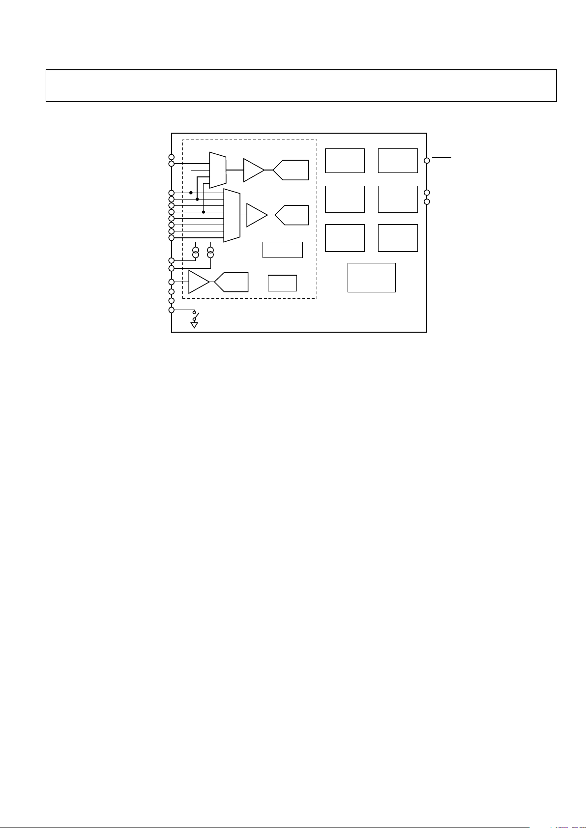
FUNCTIONAL BLOCK DIAGRAM
PRECISION ANAL OG PERIPHE RALS
POR
MEMORY
32kB FLASH
4kB RAM
ARM7TDMI
MCU
10MHz
ON-CHIP
OSC (3%)
PLL
4× TIMERS
WDT
W/U TIMER
PWM
GPIO PORT
UART PORT
SPI PORT
I
2
C PORT
VIC
(VECTORED
INTERRUPT
CONTROLL ER)
MUX
MUX
24-BIT
Σ-Δ
ADC
BUF
24-BIT
Σ-Δ ADC
PGA
PRECISION
REFERENCE
TEMP
SENSOR
14-BIT
DAC
RESET
XTAL2
XTAL1
AIN0
AIN1
AIN5
AIN4
AIN3
AIN2
AIN6
AIN7
AIN8
AIN9
IEXC0
IEXC1
DAC
VREF+
VREF–
GND_SW
ADuC7060/
ADuC7061/
ADuC7062
BUF
07079-001
Figure 1.
Page 4

ADuC7060/ADuC7061/ADuC7062 Preliminary Technical Data
Rev. PrA | Page 4 of 100
SPECIFICATIONS
ELECTRICAL SPECIFICATIONS
VDD = 2.5 V ± 5%, V
REF+
= 1.2 V, V
REF−
= GND internal reference, f
CORE
= 10.24 MHz driven from external 32.768 kHz watch crystal or on-
chip precision oscillator, all specifications T
A
= −40°C to +125°C, unless otherwise noted.
Table 1. ADuC706x Specifications
Parameter Test Conditions/Comments Min Typ Max Unit
ADC SPECIFICATIONS
Conversion Rate1 Chop off, ADC normal operating mode 50 8000 Hz
Chop on, ADC normal operating mode 4 2600 Hz
Chop on, ADC low power mode 1 650 Hz
Main Channel
No Missing Codes1 Chop off (f
ADC
≤ 1 kHz) 24 Bits
Chop on (f
ADC
≤ 666 Hz) 24 Bits
Integral Nonlinearity2 Gain = 1 ±14 ppm of FSR
Gain = 8 ±25 ppm of FSR
Gain = 64 ±66 ppm of FSR
Offset Error
3, 4
Chop off, offset error is in the order of
the noise for the programmed gain and
update rate following calibration
±4 V
Offset Error
3, 4
Chop on ±0.5 V
Offset Error Drift vs.
Temperature
5
Chop off (with GAIN ≤ 64) 650/PGA_GAIN nV/°C
Offset Error Drift vs.
Temperature
5
Chop on (with GAIN ≤ 64) 10 nV/°C
Full Scale Error
1, 6, 7, 8
Normal mode ±0.5 mV
Full Scale Error
1, 6, 7, 8
Low power mode ±1.0 mV
Gain Drift v Temperature9 5 ppm/°C
PGA Gain Mismatch Error ±0.1 %
Output Noise
1
See Table 29
Power Supply Rejection Chop on, ADC = 1 V, (gain = 1) 80 dB
Chop on, ADC = 7.8 mV, (gain = 128) 113 dB
Chop off, ADC = 1 V, (gain = 1) 80 dB
Aux Channel
No Missing Codes
1
Chop off (f
ADC
≤ 1 kHz) 24 Bits
Chop on (f
ADC
≤ 666 Hz) 24 Bits
Integral Nonlinearity ±20 ppm of FSR
Offset Error
4
Chop off ±15 V
Offset Error
4
Chop on ±0.5 V
Offset Error Drift vs.
Temperature
5
Chop off 200 nV/°C
Offset Error Drift vs.
Temperature
5
Chop on 10 nV/°C
Full-Scale Error
1, 6, 7, 8
Normal mode ±0.5 mV
Full-Scale Error
1, 6, 8
Low power mode ±1.0 mV
Gain Drift vs. Temperature9 3 ppm/°C
Output Noise See Table 27
Power Supply Rejection Chop on, ADC = 1 V 80 dB
Chop off, ADC = 1 V 80 dB
Page 5

Preliminary Technical Data ADuC7060/ADuC7061/ADuC7062
Rev. PrA | Page 5 of 100
Parameter Test Conditions/Comments Min Typ Max Unit
ADC SPECIFICATIONS: ANALOG
INPUT
Internal VREF = 1.2 V
Main Channel
Absolute Input Voltage
Range
Applies to both VIN+ and VIN− 0.1 V
DD
− 0.7 V
Input Voltage Range Gain = 11 1.2 V
Gain = 2
10
600 mV
Gain = 4
10
300 mV
Gain = 8 150 mV
Gain = 16 75 mV
Gain = 32 37.5 mV
Gain = 64 18.75 mV
Gain = 128 9.375 mV
Input Leakage Current
1
ADC0/ADC1 10 nA
ADC2/ADC3/ADC4/ADC5 15 nA
ADC6/ADC7/ADC8/ADC9 15 nA
Input Offset Current
1, 11
0.5 nA
Common-Mode Rejection
DC
1
On ADC ADC = 7.8 mV 95 dB
ADC = 1 V
1
113 dB
Common-Mode Rejection
50/60 Hz
1
50/60 Hz ± 1 Hz, 16.6 Hz and 50 Hz
update rate, chop on
ADC = 7.8 mV, range ± 20 mV 95 dB
ADC = 1 V, range ±1.2 V 90 dB
Normal-Mode Rejection
50/60 Hz
1
On ADC 50/60 Hz ± 1 Hz, 16.6Hz f
ADC
, chop on 75 dB
50/60 Hz ± 1 Hz, 16.6Hz f
ADC
, chop off 67 dB
Aux Channel
Absolute Input Voltage
Range
1
Buffer enabled 0.1 AVDD − 0.1 V
Buffer disabled AGND AVDD
Input Voltage Range Range based reference source 0 − 1.2 V
Input Current 5.5 µA
Common-Mode Rejection
DC
1
On ADC ADC = 7.8 mV 95 dB
ADC = 1 V
1
113 dB
Common-Mode Rejection
50/60 Hz
1
50/60 Hz ± 1 Hz, 16.6 Hz and 50 Hz
update rate, chop on
ADC = 7.8 mV, range ± 20 mV 95 dB
ADC = 1 V, range ± 1.2 V 90 dB
Normal-Mode Rejection
50/60 Hz
1
On ADC 50/60 Hz ± 1 Hz, 16.6 Hz f
ADC
, chop on 75 dB
50/60 Hz ± 1 Hz, 16.6 Hz f
ADC
, chop off 67 dB
VOLTAGE REFERENCE
ADC Precision Reference
Internal VREF 1.2 V
Initial Accuracy
1
Measured at TA = 25°C −0.06 +0.06 %
Reference Temperature
Coefficient
1, 12
−20 ±10 +20 ppm/°C
Power Supply Rejection 70 dB
Page 6

ADuC7060/ADuC7061/ADuC7062 Preliminary Technical Data
Rev. PrA | Page 6 of 100
Parameter Test Conditions/Comments Min Typ Max Unit
External Reference Input
Range
13
0.1 AVDD V
V
REF
Divide by 2 Initial Error
1
0.1 %
DAC CHANNEL SPECIFICATIONS RL = 5 kΩ, CL = 100 pF
Voltage Range 0 − V
REF
V
0 − AVDD V
12-BIT MODE
DC Specifications14
Resolution 12 Bits
Relative Accuracy ±2 LSB
Differential Nonlinearity Guaranteed monotonic ±0.2 ±1 LSB
Offset Error 1.2 V internal reference ±2 ±15 mV
Gain Error V
REF
range (reference = 1.2 V) ±1 %
AVDD range ±1 %
Gain Error Mismatch 0.1
% of full
scale on
DAC
16-BIT MODE
DC Specifications15
Resolution 14 Bits
Relative Accuracy For 14-bit resolution ±3 LSB
Differential Nonlinearity Guaranteed monotonic (14 bits) ±0.5 ±1 LSB
Offset Error 1.2 V internal reference ±2 ±15 mV
Gain Error V
REF
range (reference = 1.2 V) ±1 %
AVDD range ±1 %
Gain Error Mismatch 0.1
% of full
scale on
DAC
DAC AC CHARACTERISTICS
Voltage Output Settling Time 10 µs
Digital-to-Analog Glitch
Energy
1 LSB change at major carry (where
maximum number of bits
simultaneously change in the DACxDAT
register)
±20 nV-sec
TEMPERATURE SENSOR16 After user calibration
Accuracy MCU in power down or standby mode ±4 °C
Thermal Impedance 32-lead LFCSP TBD °C/W
48-lead LFCSP TBD °C/W
48-lead LFQFP TBD °C/W
POWER-ON RESET (POR)
POR Trip Level Refers to voltage at VDD pin
Power-on level 2.0 V
Power-down level 2.25 V
RESET Timeout from POR
Maximum supply ramp between 1.8 V
to 2.25 V; after POR trip, VDD must
reach 2.25 V within this time limit
128 ms
EXCITATION CURRENT SOURCES
Output Current Available from each current source 200 1000 A
Initial Tolerance at 25°C ±5 %
Drift 200 ppm/°C
Initial Current matching at
25°C
Matching between both current
sources
±0.5 %
Drift matching 20 ppm/°C
Line Regulation (AVDD) AVDD = 2.5 V ± 5% 0.2 %/V
Output Compliance1 AVDD − 0.7 AGND − 30 mV V
Page 7

Preliminary Technical Data ADuC7060/ADuC7061/ADuC7062
Rev. PrA | Page 7 of 100
Parameter Test Conditions/Comments Min Typ Max Unit
WATCHDOG TIMER (WDT )
Timeout Period
1
32.768 kHz clock, 256 prescale 0.008 512 sec
Timeout Step Size 7.8 ms
FLASH/EE MEMORY
1
Endurance17 10,000 Cycles
Data Retention
18
20 Years
DIGITAL INPUTS All digital inputs except NTRST
Input Leakage Current Input (high) = DVDD ±1 ±10 µA
Input Pull-up Current Input (low) = 0 V 10 20 80 µA
Input Capacitance 10 pF
Input Leakage Current NTRST only: input (low) = 0 V ±1 ±10 µA
Input Pull-Down Current NTRST only: input (high) = DVDD 30 55 100 µA
LOGIC INPUTS
1
All logic inputs
VINL, Input Low Voltage 0.4 V
VINH, Input High Voltage 2.0 V
CRYSTAL OSCILLATOR
1
Logic Inputs, XTAL1 Only
VINL, Input Low Voltage 0.8 V
VINH, Input High Voltage 1.7 V
XTAL1 Capacitance 12 pF
XTAL2 Capacitance 12 pF
ON-CHIP OSCILLATORS
Oscillator 32,768 kHz
Accuracy −3 +3 %
MCU CLOCK RATE
8 programmable core clock selections
within this range (binary divisions 1, 2, 4,
8 . . . 64, 128)
0.160 2.56 10.24 MHz
MCU START-UP TIME
At Power-On Includes kernel power-on execution time 134 ms
After Reset Event Includes kernel power-on execution time 5 ms
From MCU Power-Down
PLL ON
Wakeup from Interrupt 13 s
PLL Off
Wakeup from Interrupt 100 s
Internal PLL Lock Time 1 ms
POWER REQUIREMENTS
Power Supply Voltages
DVDD (±5%) 2.375 2.5 2.625 V
AVDD (±5%) 2.375 2.5 2.625 V
Power Consumption
IDD (MCU Normal Mode)19 MCU clock rate = 10.24 MHz, ADC on 10 TBC mA
MCU clock rate = 1.28 MHz, ADC on,
DAC off
2.8 mA
IDD (MCU Powered Down) 120 175 µA
IDD (Primary ADC)
PGA enabled, normal mode/low power
mode
1.2/0.3 mA
IDD (Aux ADC) Normal mode/low power mode 0.3/0.1 mA
1
These numbers are not production tested, but are guaranteed by design and/or characterization data at production release.
2
Valid for primary ADC gain setting of PGA = 4 to 64.
3
Tested at gain range = 4 after initial offset calibration.
4
Measured with an internal short. A System zero-scale calibration will remove this error.
5
Measured with an internal short.
6
These numbers do not include internal reference temperature drift.
Page 8

ADuC7060/ADuC7061/ADuC7062 Preliminary Technical Data
Rev. PrA | Page 8 of 100
7
Factory calibrated at gain = 1.
8
System calibration at specific gain range removes the error at this gain range.
9
Measured using external reference.
10
Limited by minimum absolute input voltage range.
11
Valid for a differential input less than 10 mV.
12
Measured using the box method.
13
References up to AVDD are accommodated by setting ADC0CON Bit 12.
14
Reference DAC linearity is calculated using a reduced code range of 171 to 4095.
15
Reference DAC linearity is calculated using a reduced code range of 2731 to 65,535.
16
Die temperature.
17
Endurance is qualified to 10,000 cycles as per JEDEC Std. 22 Method A117 and measured at −40°C, +25°C, and +125°C. Typical endurance at 25°C is 170,000 cycles.
18
Retention lifetime equivalent at junction temperature (TJ) = 85°C as per JEDEC Std. 22 Method A117. Retention lifetime derates with junction temperature.
19
Typical, additional supply current consumed during Flash/EE memory program and erase cycles is 7 mA and 5 mA, respectively.
TIMING SPECIFICATIONS
Data not ready yet.
Page 9
Preliminary Technical Data ADuC7060/ADuC7061/ADuC7062
Rev. PrA | Page 9 of 100
ABSOLUTE MAXIMUM RATINGS
TA = −40°C to +125°C, unless otherwise noted
Table 2.
Parameter Rating
AGND to DGND to VSS to IO_VSS −0.3 V to +0.3 V
Digital I/O Voltage to DGND −0.3 V to DVDD + 0.3 V
VREF to AGND −0.3 V to AVDD + 0.3 V
ADC Inputs to AGND −0.3 V to AVDD + +0.3 V
ESD (Human Body Model) Rating
All Pins ±2 kV
Storage Temperature 125°C
Junction Temperature
Transient 150°C
Continuous 130°C
Lead Temperature, Soldering
Reflow (15 sec)
260°C
Stresses above those listed under Absolute Maximum Ratings
may cause permanent damage to the device. This is a stress
rating only; functional operation of the device at these or any
other conditions above those indicated in the operational
section of this specification is not implied. Exposure to absolute
maximum rating conditions for extended periods may affect
device reliability.
ESD CAUTION
Page 10

ADuC7060/ADuC7061/ADuC7062 Preliminary Technical Data
Rev. PrA | Page 10 of 100
PIN CONFIGURATIONS AND FUNCTION DESCRIPTIONS
TCK
TDI
TDO
NTRST
DVDD
DGND
P2.1/PWM5/IRQ3
P1.6/PWM4
P1.5/PWM3
P1.4/PWM2
P0.2/IRQ2/PWM0
P0.4/PWM1/IRQ0
XTAL1
P0.3/MOSI/SDA
P0.2/MISO
DVDD
P0.0/SS
P0.1/SCLK/SCL
XTAL2
DGND
ADC9
ADC8
ADC6
ADC7
TMS
P1.0/IRQ1/SIN/T0
P1.1/SOUT
P0.5
P1.3/TRIP
P1.2/SYNC
RESET
P0.6
DVDD
DGND
ADC5/EXT_REF 2IN−
DAC0
ADC4/EXT_REF2I N+
ADC3
ADC2
IEXC1
IEXC0
GND_SW
ADC1
ADC0
VREF+
VREF−
AGND
AVDD
07079-002
13141516171819
2021222324
4847464544434241403938
37
1
2
3
4
5
6
7
8
9
10
11
12
35
36
34
33
32
31
30
29
28
27
26
25
ADuC7060
TOP VIEW
(Not to Scale)
PIN 1
INDICATOR
NOTES
1. NC = NO CONNE CT.
2
. THE LFCSP_VQ HAS AN EXP OSED PADDLE T HAT MUST BE CONNECT ED TO GND.
Figure 2. 48-Lead LQFPand 48-LFCSP Pin Configuration
Table 3. Pin Function Descriptions (48-Lead LQFP and 48-Lead LFCSP)
Pin No. Mnemonic
Typ e
1
Description
1
RESET
I Reset. Input pin, active low. An external 1 kΩ pull-up resistor is recommended with this pin.
2 TMS I JTAG Test Mode Select. Input pin. Used for debug and download.
3 P1.0/IRQ1/SIN/T0 I/O
General-Purpose Input and Output P1/External Interrupt Request 1/Serial Input Pin 0/Timer 0
input. This pin is a multifunction input/output pin offering four functions.
4 P1.1/SOUT I/O
General-Purpose Input and General-Purpose Output P1.1/Serial Output. This is a dual function
input/output pin.
5 P1.2/SYNC I/O
General-Purpose Input and General-Purpose Output P1.2/PWM External Sync Input. This is a dual
function input/output pin.
6 P1.3/TRIP I/O
General-Purpose Input and General-Purpose Output P1.3/PWM External Trip Input. This is a dual
function input/output pin.
7 P0.5 I/O General-Purpose Input and General-Purpose Output P0.5.
8 P0.6 I/O General-Purpose Input and General-Purpose Output P0.6.
9 DVDD S Digital Supply Pin.
10 DGND S Digital Ground.
11 DAC0 O DAC Output. Analog output pin.
12 ADC5/EXT_REF2IN− I
Single-Ended or Differential Analog Input 5/External Reference Negative Input. This is a dual
function analog input pin. The ADC5 serves as the analog input for the auxiliary ADC. The
EXT_REF2IN− serves as the external reference negative input by ADC for the auxiliary channel.
13 ADC4/EXT_REF2IN+ I
Multifunction Analog Input Pin. This pin can be used for the single-ended or differential Analog
Input 4, which is the analog input for the auxiliary ADC, or it can be used for the external
reference positive input for the auxiliary channel.
14 ADC3 I Single-Ended or Differential Analog Input 3. Analog input for the auxiliary ADC.
15 ADC2 I Single-Ended or Differential Analog Input 2. Analog input for the auxiliary ADC.
16 IEXC1 O Programmable Current Source. Analog output pin.
17 IEXC0 O Programmable Current Source. Analog output pin.
Page 11

Preliminary Technical Data ADuC7060/ADuC7061/ADuC7062
Rev. PrA | Page 11 of 100
Pin No. Mnemonic
Typ e
1
Description
18 GND_SW I
Switch to Internal Analog Ground Reference. When this input pin is not used, connect it directly
to the AGND system ground.
19 ADC1 I Positive Differential Input for Primary ADC. Analog input pin.
20 ADC0 I Negative Differential Input for Primary ADC. Analog input pin.
21 VREF+ I External Reference Positive Input for the Primary Channel. Analog input pin.
22 VREF− I External Reference Negative Input for the Primary Channel. Analog input pin.
23 AGND S Analog Ground.
24 AVDD S Analog Supply Pin.
25 ADC6 I Analog Input 6 for Auxiliary ADC. Analog input pin.
26 ADC7 I Analog Input 7 for Auxiliary ADC. Analog input pin.
27 ADC8 I Analog Input 8 for Auxiliary ADC. Analog input pin.
28 ADC9 I Analog Input 9 for Auxiliary ADC. Analog input pin.
29 DGND S Digital Ground.
30 DVDD S Digital Supply Pin.
31
P0.0/SS
I/O
Multifunction Input/Output Pin. General-Purpose Input and General-Purpose Output P0.0/SPI
slave select pin. Active low
32 P0.1/SCLK/SCL I/O
Multifunction Input/Output Pin. General-Purpose Input and General-Purpose Output P0.1/ SPI
clock pin/ I
2
C clock pin.
33 P0.2/MISO I/O
Multifunction Input/Output Pin. General-Purpose Input and General-Purpose Output P0.2/SPI
master input or slave output.
34 P0.3/MOSI/SDA I/O
Multifunction Input/Output Pin. General-Purpose Input and General-Purpose Output P0.3/ SPI
master output or slave input/I2C data pin.
35 XTAL1 O External Crystal Oscillator Output Pin.
36 XTAL2 I External Crystal Oscillator Input Pin.
37 P0.4/PWM1/IRQ0 I/O
Multifunction Input/Output Pin. General-Purpose Input and General-Purpose Output P0.4/
External Interrupt Request 0/PWM1 output.
38 P2.0/IRQ2/PWM0 I/O
Multifunction Input/Output Pin. General-Purpose Input and General-Purpose Output
P2.0/External Interrupt Request 2/PWM0 output.
39 P1.4/PWM2 I/O
Multifunction Input/Output Pin. General-Purpose Input and General-Purpose Output P1.4/PWM2
output.
40 P1.5/PWM3 I/O
Multifunction Input/Output Pin. General-Purpose Input and General-Purpose Output P1.5/PWM3
output.
41 P1.6/PWM4 I/O Multifunction I/O Pin. General-Purpose Input and General-Purpose Output P1.6/PWM4 output.
42 P2.1/PWM5/IRQ3 I/O
Multifunction Input/Output Pin. General-Purpose Input and General-Purpose Output P2.1/
PWM5 output/External Interrupt Request 3.
43 DGND S Digital Ground.
44 DVDD S Digital Supply Pin.
45 NTRST I JTAG Reset. Input pin used for debug and download only.
46 TDO O JTAG Data Out. Output pin used for debug and download only.
47 TDI I JTAG Data In. Input pin used for debug and download only.
48 TCK I JTAG Clock Pin. Input pin used for debug and download only.
1
I = input, O = output, S = supply.
Page 12

ADuC7060/ADuC7061/ADuC7062 Preliminary Technical Data
Rev. PrA | Page 12 of 100
PIN 1
INDICATO R
1RESET
2TMS
3P1.0/IRQ1/SIN/T0
4P1.1/SOUT
5DAC0
6ADC5/EXT_REF2IN−
7ADC4/EXT_REF2IN+
8ADC3
24 XT AL2
23 XT AL1
22 P0.3/MOSI/ SDA/ADC9
21 P0.2/MISO/ADC8
20 P0.1/SCLK/SCL /ADC7
19 P0.0/SS/ADC6
18 VREF–
17 VREF+
9
ADC2
10
IEXC
1
11
IEXC0
12
GND_SW
13
ADC1
14
ADC0
15
AGND
16
AVDD
32
TCK
31
TDI
30
TDO
29
NTRST
28
DVDD
27
DGND
26
P
2.0/IRQ2/PWM0
25
P0.4/IRQ0/PWM1
ADuC7061/
ADuC7062
TOP VIEW
(Not to Scale)
07079-003
NOTES
1. NC = NO CONNECT.
2. THE LFCSP_VQ HAS AN E XPOSED PADDLE THAT MUST BE CONNECTED
TO GND.
Figure 3. 32-Lead LFCSP Pin Configuration
Table 4. Pin Function Descriptions ADuC7061/ADuC7062 32-Lead LFCSP
Pin No. Mnemonic Type1 Description
1
RESET
I Reset Pin. Active Low, input pin. An external 1 kΩ pull-up resistor is recommended with this pin.
2 TMS I JTAG Test Mode Select. Input pin used for debug and download.
3 P1.0/IRQ1/SIN/T0 I/O Multifunction Input/Output Pin:
General-Purpose Input and General-Purpose Output P1.0.
External interrupt Request 1.
Serial Input.
Timer 0 Input.
4 P1.1/SOUT I/O Multifunction Input/Output Pin:
General-Purpose Input and General-Purpose Output P1.1.
Serial Output.
5 DAC0 O DAC Output. Analog output pin.
6 ADC5/EXT_REF2IN− I Multifunction Analog Input Pin:
Single-Ended or Differential Analog Input 5. Analog input for auxiliary ADC.
External Reference Negative Input for the Auxiliary Channel.
7 ADC4/EXT_REF2IN+ I Multifunction Analog Input Pin:
Single-ended or Differential Analog Input 4. Analog input for auxiliary ADC.
External Reference Positive Input for the Auxiliary Channel.
8 ADC3 I Single-Ended or Differential Analog Input 3. Analog input for auxiliary ADC.
9 ADC2 I Single-Ended or Differential Analog Input 2. Analog input for auxiliary ADC.
10 IEXC1 O Programmable Current Source. Analog output pin.
11 IEXC0 O Programmable Current Source. Analog output pin.
12 GND_SW I
Switch to Internal Analog Ground Reference. When this input pin is not used, connect it directly
to the AGND system ground.
13 ADC1 I Positive Differential Input for Primary ADC. Analog input pin.
14 ADC0 I Negative Differential Input for Primary ADC. Analog input pin.
15 AGND S Analog Ground.
16 AVDD S Analog Supply Pin.
17 VREF+ I External Reference Positive Input for the Primary Channel. Analog input pin.
18 VREF− I External Reference Negative Input for the Primary Channel. Analog input pin.
19
P0.0/SS
/ADC6
I/O
Multifunction Input/Output Pin. General-Purpose Input and General-Purpose Output P0.0/ SPI
Slave Select (active low)/Input to Auxiliary ADC6.
20 P0.1/SCLK/SDA/ADC7 I/O
Multifunction Input/Output Pin. General-Purpose Input and General-Purpose Output P0.1/SPI
clock/ I
2
C clock/ Input to Auxiliary ADC7.
Page 13

Preliminary Technical Data ADuC7060/ADuC7061/ADuC7062
Rev. PrA | Page 13 of 100
Pin No. Mnemonic Type1 Description
21 P0.2/MISO/ADC8 I/O
Multifunction Input/Output Pin. General-Purpose Input and General-Purpose Output P0.2/SPI
master input or slave output/Auxiliary ADC8 input.
22 P0.3/MOSI/SDA/ADC9 I/O
Multifunction Input/Output Pin. General-Purpose Input and General-Purpose Output P0.3/SPI
master output or slave input/I2C data pin/Auxiliary ADC ADC9 input.
23 XTAL1 O External Crystal Oscillator Output Pin.
24 XTAL2 I External Crystal Oscillator Input Pin.
25 P0.4/IRQ0/PWM1 I/O
Multifunction Input/Output Pin. General-Purpose Input and General-Purpose Output P0.4/WM1
output.
26 P2.0/IRQ2/PWM0 I/O
Multifunction Input/Output Pin. General-Purpose Input and General-Purpose Output
P2.0/External Interrupt Request 2/PWM0 output.
27 DGND S Digital Ground.
28 DVDD S Digital Supply Pin.
29 NTRST I JTAG Reset. Input pin used for debug and download only.
30 TDO O JTAG Data Out. Output pin used for debug and download only.
31 TDI I JTAG Data In. Input pin used for debug and download only.
32 TCK I JTAG Clock. Input pin used for debug and download only.
1
I = input, O = output, S = supply.
Page 14

ADuC7060/ADuC7061/ADuC7062 Preliminary Technical Data
Rev. PrA | Page 14 of 100
TERMINOLOGY
Conversion Rate
The conversion rate specifies the rate at which an output result
is available from the ADC, once the ADC has settled.
The sigma-delta (Σ-) conversion techniques used on this part
mean that while the ADC front-end signal is over sampled at a
relatively high sample rate, a subsequent digital filter is used to
decimate the output giving a valid 24-bit data conversion result
at output rates from 1 Hz to 8 kHz.
Note that when software switches from one input to another
(on the same ADC), the digital filter must first be cleared and
then allowed to average a new result. Depending on the configuration of the ADC and the type of filter, this can take
multiple conversion cycles.
Integral Nonlinearity (INL)
INL is the maximum deviation of any code from a straight line
passing through the endpoints of the transfer function. The
endpoints of the transfer function are zero scale, a point ½ LSB
below the first code transition, and full scale, a point ½ LSB
above the last code transition (111 . . . 110 to 111 . . . 111).
The error is expressed as a percentage of full scale.
No Missing Codes
No missing codes is a measure of the differential nonlinearity
of the ADC. The error is expressed in bits and specifies the
number of codes (ADC results) as 2N bits, where is N = no
missing codes, guaranteed to occur through the full ADC
input range.
Offset Error
Offset error is the deviation of the first code transition ADC
input voltage from the ideal first code transition.
Offset Error Drift
Offset error drift is the variation in absolute offset error with
respect to temperature. This error is expressed as LSBs per °C.
Gain Error
Gain error is a measure of the span error of the ADC. It is a
measure of the difference between the measured and the ideal
span between any two points in the transfer function.
Output Noise
The output noise is specified as the standard deviation (or 1 ×
Sigma) of ADC output codes distribution collected when the
ADC input voltage is at a dc voltage. It is expressed as µ rms.
The output, or rms noise, can be used to calculate the effective
resolution of the ADC as defined by the following equation:
Effective Resolution = log2(Full-Scale Range/rms Noise) bits
The peak-to-peak noise is defined as the deviation of codes that
fall within 6.6 × Sigma of the distribution of ADC output codes
collected when the ADC input voltage is at dc. The peak-topeak noise is, therefore calculated as 6.6 × the rms noise.
The peak-to-peak noise can be used to calculate the ADC
(noise free code) resolution for which there is no code flicker
within a 6.6-Sigma limit as defined by the following equation:
Noise Free Code Resolution = log2(
NoisePeaktoPeak
RangeScaleFull−−−
) bits
Data Sheet Acronyms
ADC analog-to-digital converter
ARM advanced RISC machine
JTAG joint test action group
LSB least significant byte/bit
LVF low voltage flag
MCU microcontroller
MMR memory mapped register
MSB most significant byte/bit
PID protected identifier
POR power-on reset
PSM power supply monitor
rms root mean square
Page 15

Preliminary Technical Data ADuC7060/ADuC7061/ADuC7062
Rev. PrA | Page 15 of 100
OVERVIEW OF THE ARM7TDMI CORE
The ARM7 core is a 32-bit, reduced instruction set computer
(RISC), developed by ARM® Ltd. The ARM7TDMI is a
von Neumann-based architecture, meaning that it uses a single
32-bit bus for instruction and data. The length of the data can
be 8, 16, or 32 bits and the length of the instruction word is
either 16 bits or 32 bits, depending on the mode in which the
core is operating.
The ARM7TDMI is an ARM7 core with four additional
features, as listed in Table 5.
Table 5. ARM7TDMI
Feature Description
T Support for the Thumb® (16-bit) instruction set
D Support for debug
M Enhanced multiplier
I
Includes the EmbeddedICE™ module to support
embedded system debugging
THUMB MODE (T)
An ARM instruction is 32 bits long. The ARM7TDMI processor
supports a second instruction set compressed into 16 bits, the
Thumb instruction set. Faster code execution from 16-bit memory
and greater code density is achieved by using the Thumb instruction set, making the ARM7TDMI core particularly suited for
embedded applications.
However, the Thumb mode has three limitations.
• Relative to ARM, the Thumb code usually requires more
instructions to perform that same task. Therefore, ARM
code is best for maximizing the performance of timecritical code in most applications.
• The Thumb instruction set does not include some
instructions that are needed for exception handling, so
ARM code can be required for exception handling.
• When an interrupt occurs, the core vectors to the interrupt
location in memory and executes the code present at that
address. The first command is required to be in ARM code.
MULTIPLIER (M)
The ARM7TDMI instruction set includes an enhanced
multiplier, with four extra instructions to perform 32-bit by
32-bit multiplication with a 64-bit result, and 32-bit by 32-bit
multiplication-accumulation (MAC) with a 64-bit result.
EMBEDDED ICE (I)
The EmbeddedICE module provides integrated on-chip debug
support for the ARM7TDMI. The EmbeddedICE module
contains the breakpoint and watchpoint registers that allow
nonintrusive user code debugging. These registers are controlled through the JTAG test port. When a breakpoint or
watchpoint is encountered, the processor halts and enters the
debug state. Once in a debug state, the processor registers can
be interrogated, as can the Flash/EE, SRAM, and memory
mapped registers.
ARM7 Exceptions
The ARM7 supports five types of exceptions, with a privileged
processing mode associated with each type. The five types of
exceptions are as follows:
Normal interrupt or IRQ. This is provided to service generalpurpose interrupt handling of internal and external events.
Note, that the ADuC7060 supports 8 configurable priority levels
for all IRQ sources.
Fast interrupt or FIQ. This is provided to service data transfer
or a communication channel with low latency.
FIQ has priority over IRQ. Note, that the ADuC7060 supports 8
configurable priority levels for all FIQ sources.
Memory abort (prefetch and data).
Attempted execution of an undefined instruction.
Software interrupts (SWI) instruction that can be used to make
a call to an operating system.
Typically, the programmer defines interrupts as IRQ, but for
higher priority interrupts, the programmer can define
interrupts as the FIQ type.
The priority of these exceptions and vector address are listed in
Tabl e 6.
Table 6. Exception Priorities and Vector Addresses
Priority Exception Address
1 Hardware Reset 0x00
2 Memory Abort (Data) 0x10
3 FIQ 0x1C
4 IRQ 0x18
5 Memory Abort (Prefetch) 0x0C
6 Software Interrupt1 0x08
6 Undefined Instruction1 0x04
1
A software interrupt and an undefined instruction exception have the same
priority and are mutually exclusive.
The list of exceptions in Table 6 are located from 0x00 to 0x1C,
with a reserved location at 0x14.
ARM REGISTERS
The ARM7TDMI has 16 standard registers. R0 to R12 are for
data manipulation, R13 is the stack pointer, R14 is the link
register, and R15 is the program counter that indicates the
instruction currently being executed. The link register contains
the address from which the user has branched (if the branch
and link command was used) or the command during which an
exception occurred.
The stack pointer contains the current location of the stack.
Generally, on an ARM7TDMI, the stack starts at the top of the
available RAM area and descends using the area as required. A
separate stack is defined for each of the exceptions. The size of
each stack is user configurable and is dependent on the target
application. When programming using high level languages,
Page 16
ADuC7060/ADuC7061/ADuC7062 Preliminary Technical Data
Rev. PrA | Page 16 of 100
such as C, it is necessary to ensure that the stack does not
overflow. This is dependent on the performance of the compiler
that is used.
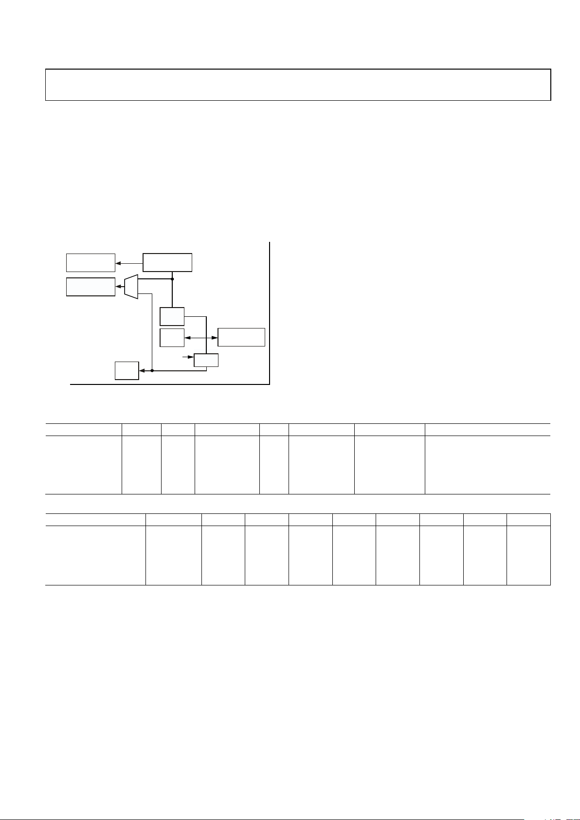
When an exception occurs, some of the standard registers are
replaced with registers specific to the exception mode. All
exception modes have replacement banked registers for the
stack pointer (R13) and the link register (R14) as represented
in Figure 4. The FIQ mode has more registers (R8 to R12)
supporting faster interrupt processing. With the increased
number of noncritical registers, the interrupt can be processed
without the need to save or restore these registers, thereby
reducing the response time of the interrupt handling process.
More information relative to the programmer’s model and the
ARM7TDMI core architecture can be found in ARM7TDMI
technical and ARM architecture manuals available directly from
ARM Ltd.
USABLE IN US ER MODE
SYSTEM MODES ONLY
SPSR_UND
SPSR_IRQ
SPSR_ABT
SPSR_SVC
R8_FIQ
R9_FIQ
R10_FIQ
R11_FIQ
R12_FIQ
R13_FIQ
R14_FIQ
R13_UND
R14_UND
R0
R1
R2
R3
R4
R5
R6
R7
R8
R9
R10
R11
R12
R13
R14
R15 (PC)
R13_IRQ
R14_IRQ
R13_ABT
R14_ABT
R13_SVC
R14_SVC
SPSR_FIQ
CPSR
USER MODE
FIQ
MODE
SVC
MODE
ABORT
MODE
IRQ
MODE
UNDEFINED
MODE
07079-004
Figure 4. Register Organization
INTERRUPT LATENCY
The worst-case latency for an FIQ consists of the longest time
the request can take to pass through the synchronizer, plus the
time for the longest instruction to complete (the longest
instruction is an LDM) that loads all the registers including the
PC, plus the time for the data abort entry, plus the time for FIQ
entry. At the end of this time, the ARM7TDMI is executing the
instruction at 0x1C (FIQ interrupt vector address). The
maximum total time is 50 processor cycles, or just over 4.88 s
in a system using a continuous 10.24 MHz processor clock. The
maximum IRQ latency calculation is similar, but must allow for
the fact that FIQ has higher priority and could delay entry into
the IRQ handling routine for an arbitrary length of time. This
time can be reduced to 42 cycles if the LDM command is not
used; some compilers have an option to compile without using
this command. Another option is to run the part in Thumb
mode where this is reduced to 22 cycles.
The minimum latency for FIQ or IRQ interrupts is five cycles.
This consists of the shortest time the request can take through
the synchronizer plus the time to enter the exception mode.
Note that the ARM7TDMI initially (first instruction) runs in
ARM (32-bit) mode when an exception occurs. The user can
immediately switch from ARM mode to Thumb mode if
required, for example, when executing interrupt service
routines.
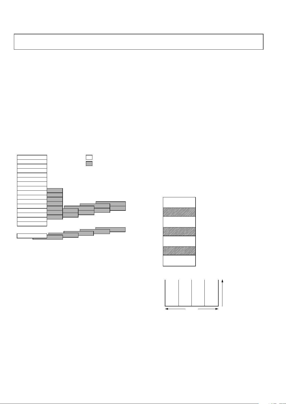
MEMORY ORGANIZATION
The ARM7, a von Neumann architecture MCU core sees
memory as a linear array of 232-byte locations. As shown in
Figure 5, the ADuC7060 maps this into four distinct user areas,
namely: a memory area that can be remapped, an SRAM area, a
Flash/EE area, and a memory mapped register (MMR) area.
The first 30 kB of this memory space is used as an area into
which the on-chip Flash/EE or SRAM can be remapped. Any
access, either reading or writing, to an area not defined in the
memory map results in a data abort exception.
Memory Format
The ADuC706x memory organization is configured in little
endian format: the least significant byte is located in the lowest
byte address and the most significant byte in the highest byte
address. See Figure 6 for details.
0x00040FFF
0x00040000
0xFFFFFFFF
0xFFFF0000
MMRs
0x00087FFF
0x00080000
FLASH/EE
SRAM
0x00007FFF
0x00000000
REMAPPABLE MEMORY SPACE
(FLASH/EE OR SRAM)
RESERVED
RESERVED
RESERVED
07079-005
Figure 5. ADuC706x Memory Map
BIT 31
BYTE 2
A
6
2
.
.
.
BYTE 3
B
7
3
.
.
.
BYTE 1
9
5
1
.
.
.
BYTE 0
8
4
0
.
.
.
BIT 0
32 BITS
0xFFFFFFFF
0x00000004
0x00000000
7079-006
Figure 6. Little Endian Format
SRAM
The ADuC706x features 4 kB of SRAM, organized as 1024 ×
32 bits, that is, 1024 words located at 0x40000.
The RAM space can be used as data memory as well as volatile
program space.
Page 17

Preliminary Technical Data ADuC7060/ADuC7061/ADuC7062
Rev. PrA | Page 17 of 100
ARM code can run directly from SRAM at full clock speed
given that the SRAM array is configured as a 32-bit wide
memory array. SRAM is read/writeable in 8-, 16-, and 32-bit
segments.
Remap
The ARM exception vectors are all situated at the bottom of the
memory array, from Address 0x00000000 to Address 0x00000020.
By default, after a reset, the Flash/EE memory is logically
mapped to Address 0x00000000.
It is possible to logically remap the SRAM to Address 0x00000000
by setting Bit 0 of the SYSMAP0 MMR located at 0xFFFF0220.
To revert Flash/EE to 0x00000000, Bit 0 of REMAP is cleared.
It is sometimes desirable to remap RAM to 0x00000000 to
optimize the interrupt latency of the ADuC706x because code
can run in full 32-bit ARM mode and at maximum core speed.
Note that when an exception occurs, the core defaults to ARM
mode.
Remap Operation
When a reset occurs on the ADuC706x, execution starts
automatically in the factory programmed internal configuration
code. This so-called kernel is hidden and cannot be accessed by
user code. If the ADuC706x is in normal mode, it executes the
power-on configuration routine of the kernel and then jumps to
the reset vector, Address 0x00000000, to execute the user’s reset
exception routine. Because the Flash/EE is mirrored at the
bottom of the memory array at reset, the reset routine must
always be written in Flash/EE.
The remap command must be executed from the absolute
Flash/EE address, and not from the mirrored, remapped
segment of memory, as this may be replaced by SRAM. If a
remap operation is executed while operating code from the
mirrored location, prefetch/data aborts can occur or the user
can observe abnormal program operation.
Any kind of reset logically remaps the Flash/EE memory to the
bottom of the memory array.
REMAP Register
Name: REMAP
Address: 0xFFFF0220
Default value: Updated by the kernel
Access: Read/write access
Function: This 8-bit register allows user code to remap
either RAM or Flash/EE space into the bottom
of the ARM memory space starting at Address
0x00000000.
Table 7. REMAP MMR Bit Designations
Bit Description
7 to 1
Reserved. These bits are reserved and should be written
as 0 by user code.
0 Remap Bit.
Set by the user to remap the SRAM to 0x00000000.
Cleared automatically after reset to remap the Flash/EE
memory to 0x00000000.
FLASH/EE CONTROL INTERFACE
Serial and JTAG programming use the Flash/EE control
interface, which includes the eight MMRs outlined in this
section.
FEESTA Register
FEESTA is a read-only register that reflects the status of the
flash control interface as described in Table 7.
Name: FEESTA
Address: 0xFFFF0E00
Default value: 0x20
Access: Read
Table 7. FEESTA MMR Bit Designations
Bit Description
15:6 Reserved.
5 Reserved.
4 Reserved.
3
Flash Interrupt Status Bit. Set automatically when an
interrupt occurs, that is, when a command is complete
and the Flash/EE interrupt enable bit in the FEEMOD
register is set. Cleared when reading FEESTA register.
2
Flash/EE Controller Busy. Set automatically when the
controller is busy. Cleared automatically when the
controller is not busy.
1
Command Fail. Set automatically when a command
completes unsuccessfully. Cleared automatically when
reading the FEESTA register.
0
Command Pass. Set by the MicroConverter® when a
command completes successfully. Cleared
automatically when reading the FEESTA register.
FEEMOD Register
FEEMOD sets the operating mode of the flash control interface.
Table 8 shows FEEMOD MMR bit designations.
Name: FEEMOD
Address: 0xFFFF0804
Default value: 0x0000
Access: Read/write
Page 18

ADuC7060/ADuC7061/ADuC7062 Preliminary Technical Data
Rev. PrA | Page 18 of 100
Table 8. FEEMOD MMR Bit Designations
Bit Description
15:9 Reserved.
8 Reserved. Always set this bit to 0.
7:5
Reserved. Always set these bits to 0 except when
writing keys.
4 Flash/EE Interrupt Enable.
Set by user to enable the Flash/EE interrupt. The
interrupt occurs when a command is complete.
Cleared by user to disable the Flash/EE interrupt.
3 Erase/Write Command Protection.
Set by user to enable the erase and write commands.
Cleared to protect the Flash against erase/write
command.
2:0 Reserved. Always set these bits to 0.
FEECON Register
FEECON is an 8-bit command register. The commands are
described in Table 9.
Name: FEECON
Address: 0xFFFF0808
Default value: 0x0
Access: Read/write
Table 9. Command Codes in FEECON
Code Command Description
0x001 Null Idle State.
0x011 Single Read Load FEEDAT with the 16-bit data. Indexed by FEEADR.
0x021 Single Write
Write FEEDAT at the address pointed by FEEADR. This operation takes 50 μs.
0x031 Erase/Write
Erase the page indexed by FEEADR and write FEEDAT at the location pointed by FEEADR. This
operation takes approximately 24 ms.
0x041 Single Verify
Compare the contents of the location pointed by FEEADR to the data in FEEDAT. The
result of the comparison is returned in FEESTA Bit 1.
0x051 Single Erase Erase the page indexed by FEEADR.
0x061 Mass Erase
Erase 30 kB of user space. The 2 kB of kernel are protected. To prevent accidental
execution, a command sequence is required to execute this instruction. See the
Command Sequence for Executing a Mass Erase section.
0x07 Reserved Reserved.
0x08 Reserved Reserved.
0x09 Reserved Reserved.
0x0A Reserved Reserved.
0x0B Signature
This command results in a 24-bit LFSR based signature been generated and loaded into
FEESIG MMR. This operation takes 16,389 clock cycles.
0x0C Protect
This command can run only once. The value of FEEPRO is saved and removed only with a
mass erase (0x06) or the key.
0x0D Reserved Reserved.
0x0E Reserved Reserved.
0x0F Ping No operation; interrupt generated.
1
The FEECON register always reads 0x07 immediately after execution of any of these commands.
Page 19

Preliminary Technical Data ADuC7060/ADuC7061/ADuC7062
Rev. PrA | Page 19 of 100
FEEDAT Register
FEEDAT is a 16-bit data register. This register holds the data
value for flash read and write commands.
Name: FEEDAT
Address: 0xFFFF080C
Default value: 0xXXXX
Access: Read/write
FEEADR Register
FEEADR is a 16-bit address register used for accessing
individual pages of the 32 kB flash block. The valid address
range for a user is: 0x0000 – 0x77FF. this represents the 30 kB
flash user memory space. A read or write access outside this
boundary causes a data abort exception to occur.
Name FEEADR
Address 0xFFFF0810
Default value 0x0000
Access Read/write
FEESIGN Register
The FEESIGN register is a 24-bit MMR. This register is updated
with the 24-bit signature value after the signature command has
been executed. This value is the result of the linear feedback
shift register (LFSR )operation initiated by the signature
command.
Name: FEESIGN
Address: 0xFFFF0818
Default value: 0xFFFFFF
Access: Read
FEEPRO Register
FEEPRO MMR provides protection following a subsequent
reset of the MMR. It requires a software key (see Table 10).
Name: FEEPRO
Address: 0xFFFF081C
Default value: 0x00000000
Access: Read/write
FEEHIDE Register
FEEHIDE MMR provides immediate protection. It does not
require any software key. Note that the protection settings in
FEEHIDE are cleared by a reset (see Table 10).
Name: FEEHIDE
Address: 0xFFFF0820
Default value: 0xFFFFFFFF
Access: Read/write
Table 10. FEEPRO and FEEHIDE MMR Bit Designations
Bit Description
31 Read Protection.
Cleared by user to protect all code. – no JTAG read
accesses for protected pages if this bit is set.
Set by user to allow reading the code via JTAG.
30
Protection for Page 59 (0x00087600 – 0x000877FF. Set
by user to allow writing the Page 59. Cleared to
protect Page 59.
29
Protection for Page 58 (0x00087400 – 0x000875FF. Set
by user to allow writing the Page 58. Cleared to
protect Page 58.
28:0
Write Protection for Page 57 to Page 0. Each bit
represents 2 pages. Each page is 512 bytes in size.
Bit0 is protection for Page 0 and Page 1 (0x00080000 –
0x000803FF. Set by the user to allow writing Page 0
and Page 1. Cleared to protect Page 0 and Page 1.
Bit1 is protection for Page 2 and Page 3 (0x00080400 –
0x000807FF. Set by the user to allow writing Page 2
and Page 3. Cleared to protect Page 2 and Page 3.
..
..
Bit27 is protection for Page 54 and Page 55
(0x00087000 – 0x000873FF. Set by the user to allow
writing Page 54 and Page 55. Cleared to protect
Page 54 and Page 55.
Bit28 is protection for Page 56 and Page 57
(0x00087400 – 0x000877FF. Set by the user to allow
writing Page 56 and Page 57. Cleared to protect
Page 56 and Page 57.
Command Sequence for Executing a Mass Erase
FEEDAT = 0x3CFF;
FEEADR = 0x77C3;
FEEMOD = FEEMOD|0x8; //Erase key enable
FEECON = 0x06; //Mass erase command
Page 20

ADuC7060/ADuC7061/ADuC7062 Preliminary Technical Data
Rev. PrA | Page 20 of 100
MEMORY MAPPED REGISTERS
The memory mapped register (MMR) space is mapped into the
upper two pages of the memory array, and accessed by indirect
addressing through the ARM7 banked registers.
The MMR space provides an interface between the CPU and all
on-chip peripherals. All registers, except the core registers,
reside in the MMR area. All shaded locations shown in 5 are
unoccupied or reserved locations, and should not be accessed
by user software. Figure 7 shows the full MMR memory map.
The access time for reading from or writing to an MMR
depends on the advanced microcontroller bus architecture
(AMBA) bus used to access the peripheral. The processor has
two AMBA busses: advanced high performance bus (AHB)
used for system modules, and advanced peripheral bus (APB)
used for a lower performance peripheral. Access to the AHB is
one cycle, and access to the APB is two cycles. All peripherals
on the ADuC706x are on the APB except the Flash/EE memory,
the GPIOs, and the PWM.
PWM
0xFFFF0FC0
0xFFFFFFF
F
0xFFFF 0F80
FLASH CONTRO L
INTERFACE
0xFFFF0E24
0xFFFF0E00
GPIO
0xFFFF0D50
0xFFFF0D00
SPI
0xFFFF0A14
0xFFFF0A00
I2C
0xFFFF 0948
0xFFFF 0900
UART
0xFFFF 0730
0xFFFF 0700
DAC
0xFFFF 0620
0xFFFF 0600
ADC
0xFFFF 0570
0xFFFF 0500
BANDGAP
REFERENCE
0xFFFF 0490
0xFFFF 048C
SPI/I2C
SELECTION
0xFFFF 0470
0xFFFF 0450
PLL AND OSCI LLATOR
CONTROL
0xFFFF 0420
0xFFFF 0404
GENERAL PURPOS E
TIMER
0xFFFF 0394
0xFFFF 0380
WATCHDOG
TIMER
0xFFFF 0370
0xFFFF 0360
WAKE UP
TIMER
0xFFFF 0350
0xFFFF 0340
GENERAL PURPOS E
TIMER
0xFFFF 0334
0xFFFF 0320
REMAP AND
SYSTEM CONTROL
0xFFFF 0238
0xFFFF 0220
INTERRUPT
CONTROLL ER
0xFFFF 0140
0xFFFF 0000
07079-007
Figure 7. Memory Mapped Registers
Page 21

Preliminary Technical Data ADuC7060/ADuC7061/ADuC7062
Rev. PrA | Page 21 of 100
COMPLETE MMR LISTING
In the following MMR tables, addresses are listed in hex code. Access types include R for read, W for write, and RW for read and write.
Table 11. IRQ Address Base = 0xFFFF0000
Address Name Byte
Access
Typ e
Default
Value Description
0x0000 IRQSTA 4 R 0x00000000 Active IRQ Source.
0x0004 IRQSIG 4 R Current State of All IRQ Sources (Enabled and Disabled).
0x0008 IRQEN 4 RW 0x00000000 Enabled IRQ Sources.
0x000C IRQCLR 4 W MMR to Disable IRQ Sources.
0x0010 SWICFG 4 W Software Interrupt Configuration MMR.
0x0014 IRQBASE 4 R/W 0x00000000
Base Address of all Vectors. Points to start of 64-byte memory block
which can contain up to 32 pointers to separate subroutine handlers.
0x001C IRQVEC 4 R 0x00000000
This register contains the subroutine address for the currently active IRQ
source.
0x0020 IRQP0 4 R/W 0x00000000
Contains the interrupt priority setting for interrupt Source 1 to Source 7.
An interrupt can have a priority setting of 0 to 7. For example:
Bits[7:4] containthe priority level for Interrupt 1.
Bits[11:8] contain the priority level for Interrupt 2.
Bits[31:28] contain the priority level for Interrupt 7.
0x0024 IRQP1 4 R/W 0x00000000
Contains the interrupt priority setting for Interrupt Source 8 to Interrupt
Source 15. For example:
Bits[7:4] contain the priority level for Interrupt 9.
Bits[11:8] contain the priority level for Interrupt 10.
Bits[31:28] contain the priority level for Interrupt 15.
0x0028 IRQP2 4 R/W 0x00000000
Contains the interrupt priority setting for Interrupt Source 16 to Interrupt
Source 19.
0x002C RESERVED 4 R/W 0x00000000 Reserved.
0x0030 IRQCONN 4 R/W 0x00000000 Used to enable IRQ and FIQ interrupt nesting.
0x0034 IRQCONE 4 R/W 0x00000000
Configures the external interrupt sources as either rising edge, falling
edge, or level triggered.
0x0038 IRQCLRE 4 R/W 0x00000000 Used to clear an edge level triggered interrupt source.
0x003C IRQSTAN 4 R/W 0x00000000
This register indicates the priority level of an interrupt that has just
caused an interrupt exception.
0x0100 FIQSTA 4 R 0x00000000 Active FIQ Source.
0x0104 FIQSIG 4 R Current State of All FIQ Sources (Enabled and Disabled).
0x0108 FIQEN 4 RW 0x00000000 Enabled FIQ Sources.
0x010C FIQCLR 4 W MMR to Disable FIQ Sources.
0x011C FIQVEC 4 R 0x00000000 FIQ Interrupt Vector.
0x013C FIQSTAN 4 R 0x00000000
Indicates the priority level of an FIQ that has just caused an FIQ
exception.
Table 12. System Control Address Base = 0xFFFF0200
Address Name Byte
Access
Typ e
Default Value Description
0x0220 REMAP1 1 R/W 0x00 REMAP Control Register. See the Remap Operation section.
0x0230 RSTSTA 1 R/W 0x01 RSTSTA Status MMR. See the Reset section.
0x0234 RSTCLR 1 W 0x00 RSTCLR MMR for clearing RSTSTA register.
1
Updated by kernel.
Page 22

ADuC7060/ADuC7061/ADuC7062 Preliminary Technical Data
Rev. PrA | Page 22 of 100
Table 13. Timer Address Base = 0xFFFF0300
Address Name Byte
Access
Type Default Value Description
0x0320 T0LD 4 RW 0x00000000 Timer0 Load Register.
0x0324 T0VAL 4 R 0xFFFFFFFF Timer0 Value Register.
0x0328 T0CON 4 RW 0x01000000 Timer0 Control MMR.
0x032C T0CLRI 1 W N/A Timer0 Interrupt Clear Register.
0x0330 T0CAP 4 R 0x00000000 Timer0 Capture Register.
0x0340 T1LD 4 RW 0x00000000 Timer1 Load Register.
0x0344 T1VAL 4 R 0xFFFFFFFF Timer1 Value Register
0x0348 T1CON 2 RW 0x0000 Timer1 Control MMR.
0x034C T1CLRI 1 W N/A Timer1 Interrupt Clear Register
0x0360 T2LD 2 RW 0x0040 Timer2 Load Register.
0x0364 T2VAL 2 R 0x0040 Timer2 Value Register.
0x0368 T2CON 2 RW 0x0100 Timer2 Control MMR.
0x036C T2CLRI 1 W N/A Timer2 Interrupt Clear Register.
0x0380 T3LD 2 RW 0x0000 Timer3 Load Register.
0x0384 T3VAL 2 R 0xFFFF Timer3 Value Register.
0x0388 T3CON 4 RW 0x00000000 Timer3 Control MMR.
0x038C T3CLRI 1 W N/A Timer3 Interrupt Clear Register.
0x0390 T3CAP 2 R 0x0000 Timer3 Capture Register.
Table 14. PLL Base Address = 0xFFFF0400
Address Name Byte
Access
Typ e
Default Value Description
0x0404 POWKEY1 2 W N/A POWCON Prewrite Key
0x0408 POWCON0 1 RW 0x7B Power Control and Core Speed Control Register.
0x040C POWKEY2 4 W N/A POWCON Postwrite Key..
0x0410 PLLKEY1 4 W N/A PLLCON Prewrite Key.
0x0414 PLLCON 1 RW 0x00 PLL Clock Source Selection MMR.
0x0418 PLLKEY2 4 W N/A PLLCON Postwrite Key.
0x0464 GP0KEY1 4 R/W 0x00 GP0CON1 Prewrite Key.
0x0468 GP0CON1 1 R/W 0x00
Configures P0.0, P0.1, P0.2, and P0.3 as analog inputs or digital I/Os. Also
enables SPI or I
2
C mode.
0x046C GP0KEY2 4 R/W 0x00 GP0CON1 Postwrite Key.
Page 23

Preliminary Technical Data ADuC7060/ADuC7061/ADuC7062
Rev. PrA | Page 23 of 100
Table 15. ADC Address Base = 0xFFFF0500
Address Name Byte
Access
Type Default Value Description
0x0500 ADCSTA 2 R 0x0000 ADC Status MMR.
0x0504 ADCMSKI 2 R/W 0x0000 ADC Interrupt Source Enable MMR.
0x0508 ADCMDE 2 R/W 0x0003 ADC Mode Register.
0x050C ADC0CON 2 R/W 0x8000 Primary ADC Control MMR.
0x0510 ADC1CON 2 R/W 0x0000 Auxiliary ADC Control MMR.
0x0514 ADCFLT 2 R/W 0x0007 ADC Filter Control MMR.
0x0518 ADCCFG 2 R/W 0x0000 ADC Configuration MMR.
0x051C ADC0DAT 4 R/W 0x00000000 Primary ADC Result MMR.
0x0520 ADC1DAT 4 R/W 0x00000000 Auxiliary ADC Result MMR
0x0524 ADC0OF 2 R/W 0x0000 Primary ADC Offset Calibration Setting.
0x0528 ADC1OF 2 R/W 0x0000 Auxiliary ADC Offset MMR.
0x052C ADC0GN 2 R/W 0x5555 Primary ADC Offset MMR.
0x0530 ADC1GN 2 R/W 0x5555 Auxiliary ADC Offset MMR. See the Gain Calibration section.
0x0534 ADCORCR 2 R/W 0x0001 Primary ADC Result Counter/Reload MMR.
0x0538 ADCORCV 2 R 0x0000 Primary ADC Result Counter MMR.
0x053C ADCOTH 2 R/W 0x0000 Primary ADC 16-bit Comparator Threshold MMR.
0x0540 ADCOTHC 2 R/W 0x0001 Primary ADC 16-bit Comparator Threshold Counter Limit.
0x0544 ADCOTHV 2 R/W 0x0000
0x0548 ADCOACC 4 R/W 0x00000000 Primary ADC Accumulator.
0x054C ADCOATH 4 R/W 0x00000000 Primary ADC 32-Bit Comparator Threshold MMR.
0x0570 IEXCON 1 R/W 0x00 Excitation Current Sources Control Register.
1
Updated by kernel. {Where is this endnote in the table?}
Table 16. DAC Control Address Base = 0xFFFF0600
Address Name Byte
Access
Type Default Value Description
0x0600 DACCON 1 R/W 0x00 DAC Control Register.
0x0604 DAC0DAT 4 R/W 0x00000000 DAC Output Data Register.
Table 17. UART Base Address = 0XFFFF0700
Address Name Byte
Access
Type Default Value Description
0x0700 COMTX 1 W N/A UART Transmit Register.
0x0700 COMRX 1 R 0x00 UART Receive Register.
0x0700 COMDIV0 1 RW 0x00 UART Standard Baud Rate Generator Divisor Value 0.
0x0704 COMIEN0 1 RW 0x00 UART Interrupt Enable MMR 0.
0x0704 COMDIV1 1 R/W 0x00 UART Standard Baud Rate Generator Divisor Value 1.
0x0708 COMIID0 1 R 0x01 UART Interrupt Identification 0.
0x070C COMCON0 1 RW 0x03 UART Control Register 0.
0x0710 COMCON1 1 RW 0x00 UART Control Register 1.
0x0714 COMSTA0 1 R 0x60 UART Status Register 0.
0X072C COMDIV2 2 RW 0x0000 UART Fractional Divider MMR.
Page 24

ADuC7060/ADuC7061/ADuC7062 Preliminary Technical Data
Rev. PrA | Page 24 of 100
Table 18. I2C Base Address = 0XFFFF0900
Address Name Byte
Access
Typ e
Default
Value Description
0x0900 I2CMCON 2 R/W 0x0000 I2C master Control register.
0x0904 I2CMSTA 2 R 0x0000 I2C master Status register.
0x0908 I2CMRX 1 R 0x00 I2C master Receive register.
0x090C I2CMTX 1 W 0x00 I2C master Transmit register.
0x0910 I2CMCNT0 2 R/W 0x0000
I
2
C master Read Count register. Write the number of required bytes into this
register prior to reading from a slave device.
0x0914 I2CMCNT1 1 R 0x00
I
2
C master Current Read count register. This register contains the number of
bytes already received during a read from slave sequence.
0x0918 I2CADR0 1 R/W 0x00
Address byte register. Write the required slave address in here prior to
communications.
0x091C I2CADR1 1 R/W 0x00
Address byte register. Write the required slave address in here prior to
communications. Only used in 10-bit mode.
0x0924 I2CDIV 2 R/W 0x1F1F I2C clock control register. Used to configure the SCLK frequency.
0x0928 I2CSCON 2 R/W 0x0000 I2C slave Control register.
0x092C I2CSSTA 2 R/W 0x0000 I2C slave Status register.
0x0930 I2CSRX 1 R/W 0x00 I2C slave Receive register.
0x0934 I2CSTX 1 R/W 0x00 I2C slave Transmit register.
0x0938 I2CALT 1 R/W 0x00 I2C Hardware General Call recognition register.
0x093C I2CID0 1 R/W 0x00 I2C Slave ID0 register. Slave bus ID register
0x0940 I2CID1 1 R/W 0x00 I2C Slave ID1 register. Slave bus ID register
0x0944 I2CID2 1 R/W 0x00 I2C Slave ID2 register. Slave bus ID register
0x0948 I2CID3 1 R/W 0x00 I2C Slave ID3 register. Slave bus ID register
0x094C I2CFSTA 2 R/W 0x0000 I2C FIFO Status register. Used in both master + slave modes
Table 19. SPI Base Address = 0xFFFF0A00
Address Name Byte Access Type Default Value Description
0x0A00 SPISTA 4 R 0x00000000 SPI Status MMR.
0x0A04 SPIRX 1 R 0x00 SPI Receive MMR.
0x0A08 SPITX 1 W SPI Transmit MMR.
0x0A0C SPIDIV 1 RW 0x1B SPI Baud Rate Select MMR.
0x0A10 SPICON 2 RW 0x00 SPI Control MMR.
Table 20. GPIO Base Address = 0xFFFF0D00
Address Name Byte
Access
Type Default Value Description
0x0D00 GP0CON 4 RW 0x00000000 GPIO Port0 Control MMR.
0x0D04 GP1CON 4 RW 0x00000000 GPIO Port1 Control MMR.
0x0D08 GP2CON 4 RW 0x00000000 GPIO Port2 Control MMR.
0x0D20 GP0DAT 4 RW 0x000000EF GPIO Port0 Data Control MMR.
0x0D24 GP0SET 4 W 0x000000EF GPIO Port0 Data Set MMR.
0x0D28 GP0CLR 4 W 0x000000EF GPIO Port0 Data Clear MMR.
0x0D2C GP0PAR 4 W 0x00000000 GPIO Port0 Pull-Up Disable MMR.
0x0D30 GP1DAT 4 RW 0x000000FF GPIO Port1 Data Control MMR.
0x0D34 GP1SET 4 W 0x000000FF GPIO Port1 Data Set MMR.
0x0D38 GP1CLR 4 W 0x000000FF GPIO Port1 Data Clear MMR.
0x0D3C GP1PAR 4 W 0x00000000 GPIO Port1 Pull-Up Disable MMR.
0x0D40 GP2DAT 4 RW 0x000000FF GPIO Port2 Data Control MMR.
0x0D44 GP2SET 4 W 0x000000FF GPIO Port2 Data Set MMR.
0x0D48 GP2CLR 4 W 0x000000FF GPIO Port2 Data Clear MMR.
0x0D4C GP2PAR 4 W 0x00000000 GPIO Port2 Pull-up Disable MMR.
Page 25

Preliminary Technical Data ADuC7060/ADuC7061/ADuC7062
Rev. PrA | Page 25 of 100
Table 21. Flash/EE Base Address = 0xFFFF0E00
Address Name Byte
Access
Type Default Value Description
0x0E00 FEESTA 1 R 0x20 Flash/EE Status MMR.
0x0E04 FEEMOD 1 RW 0x00 Flash/EE Control MMR.
0x0E08 FEECON 1 RW 0x07 Flash/EE Control MMR.
0x0E0C FEEDAT 2 RW 0x0000 Flash/EE Data MMR.
0x0E10 FEEADR 2 RW 0x0000 Flash/EE Address MMR.
0x0E18 FEESIG 3 R 0xFFFFFF Flash/EE LFSR MMR.
0x0E1C FEEPRO 4 RW 0x00000000 Flash/EE Protection MMR.
0x0E20 FEEHID 4 RW 0xFFFFFFFF Flash/EE Protection MMR.
Table 22. PWM Base Address = 0xFFFF0F80
Address Name Byte
Access
Type Default Value Description
0x0F80 PWMCON 2 R/W 0x0000 PWM Control register. See PWM section for full details.
0x0F84 PWM0COM0 2 R/W 0x0000 Compare Register 0 for PWM Output 0 and PWM Output 1.
0x0F88 PWM0COM1 2 R/W 0x0000 Compare Register 1 for PWM Output 0 and PWM Output 1.
0x0F8C PWM0COM2 2 R/W 0x0000 Compare Register 2 for PWM Output 0 and PWM Output 1.
0x0F90 PWM0LEN 2 R/W 0x0000 Frequency Control for PWM outputs 0 and PWM Output 1.
0x0F94 PWM1COM0 2 R/W 0x0000 Compare Register 0 for PWM Output 2 and PWM Output 3.
0x0F98 PWM1COM1 2 R/W 0x0000 Compare Register 1 for PWM Output 2 and PWM Output 3.
0x0F9C PWM1COM2 2 R/W 0x0000 Compare Register 2 for PWM Output 2 and PWM Output 3.
0x0FA0 PWM1LEN 2 R/W 0x0000 Frequency Control for PWM Output 2 and PWM Output 3.
0x0FA4 PWM2COM0 2 R/W 0x0000 Compare Register 0 for PWM Output 4 and PWM Output 5.
0x0FA8 PWM2COM1 2 R/W 0x0000 Compare Register 1 for PWM Output 4 and PWM Output 5.
0x0FAC PWM2COM2 2 R/W 0x0000 Compare Register 2 for PWM Output 4 and PWM Output 5.
0x0FB0 PWM2LEN 2 R/W 0x0000 Frequency Control for PWM Output 4 and PWM Output 5.
0x0FB8 PWMCLRI 2 R/W 0x0000
PWM Interrupt Clear Register. Writing any value to this register clears a
PWM interrupt source.
Page 26

ADuC7060/ADuC7061/ADuC7062 Preliminary Technical Data
Rev. PrA | Page 26 of 100
RESET
There are four kinds of reset: external reset, power-on-reset,
watchdog reset, and software reset. The RSTSTA register
indicates the source of the last reset and can be written by user
code to initiate a software reset event.
The bits in this register can be cleared to 0 by writing to the
RSTCLR MMR at 0xFFFF0234. The bit designations in
RSTCLR mirror those of RSTSTA. These registers can be used
during a reset exception service routine to identify the source of
the reset. The implications of all four kinds of reset events are
tabulated in Table 24.
RSTSTA Register
Name: RSTSTA
Address: 0xFFFF0230
Default value: Depends on type of reset
Access: Read/write access
Function: This 8-bit register indicates the source of the
last reset event and can be written by user code
to initiate a software reset.
RSTCLR Register
Name: RSTCLR
Address: 0xFFFF0234
Access: Write only
Function: This 8-bit write only register clears the
corresponding bit in RSTSTA.
Table 23. RSTSTA/RSTCLR MMR Bit Designations
Bit Description
7 to 4
Not Used. These bits are not used and always
read as 0.
3 External Reset.
Automatically set to 1 when an external reset
occurs.
This bit is cleared by setting the corresponding bit
in RSTCLR.
2 Software Reset.
This bit is set to 1 by user code to generate a software reset.
This bit is cleared by setting the corresponding bit
in RSTCLR.
1
1 Watchdog Timeout.
Automatically set to 1 when a watchdog timeout
occurs.
Cleared by setting the corresponding bit in RSTCLR.
0 Power-On Reset.
Automatically Set when a power-on-reset occurs.
Cleared by setting the corresponding bit in RSTCLR.
1
If the software reset bit in RSTSTA is set, any write to RSTCLR that does not
clear this bit generates a software reset.
Table 24. Device Reset Implications
RESET
Reset External
Pins to Default
State
Kernel
Executed
Reset All
External MMRs
(Excluding
RSTSTA)
Peripherals
Reset
Watc hdog
Timer Reset
RAM
Valid
RSTSTA (Status
After Reset
Event)
POR Yes Yes Yes Yes Yes Yes/No RSTSTA[0] = 1
Watchdog Yes Yes Yes Yes No Yes RSTSTA[1] = 1
Software Yes Yes Yes Yes No Yes RSTSTA[2] = 1
External
Pin
Yes Yes Yes Yes No Yes RSTSTA[3] = 1
Page 27
Preliminary Technical Data ADuC7060/ADuC7061/ADuC7062
Rev. PrA | Page 27 of 100
OSCILLATOR, PLL AND POWER CONTROL
Clocking System
Each ADuC7060 integrates a 32.768 kHz ±3% oscillator, a clock
divider, and a PLL. The PLL locks onto a multiple of the internal
oscillator or an external 32.768 kHz crystal to provide a stable 10.24
MHz clock (UCLK) for the system. To allow power saving, the core
can operate at this frequency, or at binary submultiples of it. The
actual core operating frequency, UCLK/2
CD
, is refered to as HCLK.
The default core clock is the PLL clock divided by 8 (CD = 3) or
1.28 MHz.
PLL
CORE
CD
10.24MHz
32.768kHz
*32.768kHz±3%
HCLK
UCLK
OCLK
WATCHDOG
TIMER
WAKEUP
TIMER
INT. 32kHz
OSCILLATOR
ANALOG
PERIPHERALS
/2
CD
I2C
07079-008
Figure 8. Clocking System
The selection of the clock source is in the PLLCON register. By
default, the part uses the internal oscillator feeding the PLL.
Power Control System
The core clock frequency is changed by writing to the POWCON0
register. This is a key protected register therefore, registers
POWKEY1 and POWKEY2 must be written to immediately before
and after configuring the POWCON0 register. The following is a
simple example showing how to configure the core clock for
10.24 MHz:
POWKEY1 = 0x1;
POWCON0 = 0x78; //Set core to max CPU
//speed of 10.24 MHz
POWKEY2 = 0xF4;
A choice of operating modes is available on the ADuC7060. Table
below describes what part is powered on in the different modes and
indicates the power-up time.
Table 26 gives some typical values of the total current consumption
(analog + digital supply currents) in the different modes, depending
on the clock divider bits. The ADC is turned off. Note that these
values also include current consumption of the regulator and other
parts on the test board where these values are measured.
Table 25.
POWCON[6:3] Mode Core Peripherals PLL XTAL/T2/T3 IRQ0 to IRQ3 Start-Up/Power-On Time
1111 Active X X X X X
1110 Pause X X X X
1100 Nap X X X
1000 Sleep X X
0000 Stop X
Table 26. Typical Current Consumption at 25°C in mA
POWCON[6:3] Mode CD = 0 CD = 1 CD = 2 CD = 3 CD = 4 CD = 5 CD = 6 CD = 7
1111 Active TBD TBD TBD TBD TBD TBD TBD TBD
1110 Pause TBD TBD TBD TBD TBD TBD TBD TBD
1100 Nap TBD TBD TBD TBD TBD TBD TBD TBD
1000 Sleep TBD TBD TBD TBD TBD TBD TBD TBD
0000 Stop TBD TBD TBD TBD TBD TBD TBD TBD
Page 28

ADuC7060/ADuC7061/ADuC7062 Preliminary Technical Data
Rev. PrA | Page 28 of 100
Power and Clock Control Registers
Name: POWKEY1
Address: 0xFFFF0404
Default Value: 0xXXXX
Access: Write
Function: When writing to POWCON0, the value 0x01
must be written to this register in the
instruction immediately before writing to
POWCON0
Name: POWCON0
Address: 0xFFFF0408
Default Value: 0x7B
Access: Read/write
Function: This register controls the clock divide bits
controlling the CPU clock (HCLK)
Table 27. POWCON0 MMR Bit Designations
Bit Name Description
7 Reserved This bit must always be set to 0.
6 XPD
XTAL Power Down.
Cleared by the user to power-down the external crystal circuitry.
Set by the user to enable the external crystal circuitry.
5
PLLPD
PLL Power Down. Timer peripherals power down if driven from the PLL output clock.
Timers driven from an active clock source remain in normal power mode.
This bit is cleared to 0 to power-down the PLL.
The PLL cannot be powered down if either the core or peripherals are enabled:
Bit 3, Bit 4, and Bit 5 must be cleared simultaneously.
Set by default, and set by hardware on a wake-up event.
4
PPD
Peripherals Power Down. The peripherals that are powered down by this bit are as follows:
SRAM, Flash/EE memory and GPIO interfaces, and SPI/I
2
C and UART serial ports.
Cleared to power-down the peripherals. The peripherals cannot be powered down if the core is enabled:
Bit 3 and Bit 4 must be cleared simultaneously.
Set by default, and/or by hardware, on a wake-up event. Wake-up timer (Timer1) can still be active
3
COREPD
Core Power Down. If user code powers down the MCU, include a dummy MCU cycle after the power-down
command is written to POWCON.
Cleared to power-down the ARM core.
Set by default and set by hardware on a wake-up event.
2 to 0 CD[2:0] Core clock depends on CD setting:
[000] = 10.24 MHz
[001] = 5.12 MHz
[010] = 2.56 MHz
[011] = 1.28 MHz [default value]
[100] = 640 kHz
[101] = 320 kHz
[110] = 160 kHz
[111] = 80 kHz
Page 29

Preliminary Technical Data ADuC7060/ADuC7061/ADuC7062
Rev. PrA | Page 29 of 100
Name: POWKEY2
Address: 0xFFFF040C
Default Value: 0xXXXX
Access: Write
Function: When writing to POWCON0, the value 0xF4 must be written to this register in the instruction immediately
after writing to POWCON0
Name: PLLKEY1
Address: 0xFFFF0410
Default Value: 0xXXXX
Access: Write
Function: When writing to the PLLCON register, the value 0xAA must be written to this register in the instruction
immediately before writing to PLLCON
Name: PLLCON
Address: 0xFFFF0414
Default Value: 0x00
Access: Read/Write
Function: This register selects the clock input to the PLL.
Table 28. PLLCON MMR Bit Designations
Bit Name Description
7 to 2 Reserved These bits must always be set to 0.
1 to 0 OSEL Oscillator Selection bits:
[00] = Internal 32,768 Hz Oscillator
[01] = Internal 32,768 Hz Oscillator
[10] = External Crystal
[11] = Internal 32,768 Hz Oscillator
Name: PLLKEY2
Address: 0xFFFF0418
Default Value: 0xXXXX
Access: Write
Function: When writing to PLLCON, the value 0x55 must be written to this register in the instruction immediately after
writing to PLLCON.
Page 30
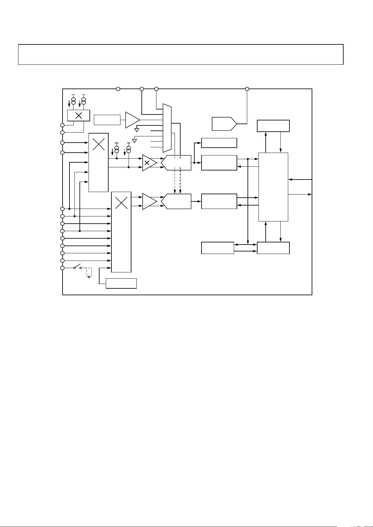
ADuC7060/ADuC7061/ADuC7062 Preliminary Technical Data
Rev. PrA | Page 30 of 100
ADC CIRCUIT INFORMATION
IEXC0
IEXC1
AIN2
AIN3
AIN4
AIN5
AIN6
AIN7
AIN8
AIN9
GND_SW
50Ω
BUF
Σ-Δ
MODULATOR
PROGRAMMABLE
FILTER
Σ-Δ
MODULATOR
PROGRAMMABLE
FILTER
OVERRANGE
INTERFACE
AND CONTROL
CHOP
MUX
CHOP
MUX
AGND
TEMPERATURE
SENSOR
INTEGRATOR
ACCUMULATOR
CONVERSION
COUNTER
COMPARATORS
TO ARM
0.2Hz TO 8kHz
0.5Hz TO 8kHz
DAC
BUF
INTERNAL
REFERENCE
AVDD
EXT_REF2IN+
EXT_REF2IN−
0.2mA TO 1mA
PGA
50µA O/C
DETECT
V
REF–
V
REF+AVDD
AIN0
AIN1
DAC0
07079-009
Figure 9. Analog Block Diagram
The ADuC706x incorporates two independent multichannel
Σ- ADCs. The primary ADC is a 24-bit, 5-channel ADC. The
auxiliary ADC is a 16-bit Σ- ADC, with up to eight input
channels.
The primary ADC input has a mux and a programmable gain
amplifier on its input stage. The mux on the primary channel
can be configured as two fully differential input channels or five
single-ended input channels.
The auxiliary ADC incorporates a buffer on its input stage.
Digital filtering is present on both ADCs which allows
measurement of a wide dynamic range and low frequency
signals such as those in pressure sensor, temperature sensor,
weigh-scale, or strain-gauge type applications.
The ADuC706x auxiliary ADC can be configured as four fully
differential input channels or as eight single-ended input
channels.
Because of internal buffering, the internal channels can convert
signals directly from sensors without the need for external
signal conditioning.
Page 31

Preliminary Technical Data ADuC7060/ADuC7061/ADuC7062
Rev. PrA | Page 31 of 100
Table 29. Primary ADC: Typical Output RMS noise in Normal Mode
ADC
Register
Data
Update
Rate
±2.34 mV
(512)
±4.68 mV
(256)
±9.375 mV
(128)
±18.75 mV
(64)
±37.5 mV
(32)
±75 mV
(16)
±150 mV
(8)
±300 mV
(4)
±600 mV
(2)
±1.2 V
(1)
(Chop
On)
4 Hz 0.033 V 0.032 V 0.0338 V 0.032 V 0.041 V 0.077 V 0.109 V 0.175V 0.648 V 0.62 V
(Chop
Off)
50 Hz 0.098 V 0.098 V 0.12 V 0.123 V 0.147 V 0.27 V 0.38 V 0.570 V 1.89 V 1.97 V
(Chop
Off)
1 kHz 0.52 V 0.56 V 0.55 V 0.53 V 0.658 V 1.17 V 1.6 V 2.55 V 8.4 V 8.54 V
(Chop
Off)
8 kHz 0.909 V 0.915 V 1.75 V 1.71 V 2.5 V 4.59 V 7.88 V 14.30 V 55.54 V 54.97 V
Table 30. Auxillary ADC: Typical Output RMS Noise
ADC Register
Data Update
Rate RMS value
Chop On 4 Hz 0.633 V
Chop On 10 Hz 0.810 V
Chop Off 1 kHz 7.4 V
Chop Off 8 kHz 54.18 V
Reference Sources
Both the primary and secondary ADCs have the option of using
the internal reference voltage or, one of two external differential
reference sources. The first external reference is applied to the
VREF+/VREF− pins. The second external reference is applied
to the ADC4 (EXT_VREF2+) and ADC5 (EXT_VREF2−) pins.
By default, each ADC uses the internal 1.2 V reference source.
For details on how to configure the external reference source for
the primary ADC, see the description of the ADC0REF[1:0]
bits in the ADC0 control register, ADC0CON.
For details on how to configure the external reference source for
the auxiliary ADC, see the description of the ADC1REF[2:0]
bits in the ADC1 control register, ADC1CON.
If an external reference source of greater than 1.35 V is needed
for ADC0, the HIGHEXTREF0 bit must be set in ADC0CON.
Similarly, if an external reference source of greater than 1.35 V
is used for ADC1, set the HIGHEXTREF1 bit in ADC1CON.
Note, if an external reference source of greater than 1.35 V is
used for ADC0, the HIGHEXTREF0 bit must be set in
ADC0CON. Similarly, an external reference source of greater
than 1.35 V is used for ADC1, the HIGHEXTREF1 bit must be
set in ADC1CON.
Diagnostic Current Sources
To detect a connection failure to an external sensor, the
ADuC706x incorporates 50 A constant current sources on the
selected analog input channels to both the primary and
auxiliary ADCs.
The diagnostic current sources for the primary ADC analog
inputs are controlled by the ADC0DIAG[1:0] bits in the
ADC0CON register.
Similarly, the diagnostic current sources for the auxiliary ADC
analog inputs are controlled by the ADC1DIAG[1:0] bits in the
ADC0CON register.
AIN1 (–)
AIN0 (+)
AVDD
R1
AB
R2
AB
VIN =
AIN0,
AIN1
07079-010
Figure 10. Example Circuit Using Diagnostic Current Sources
Page 32

ADuC7060/ADuC7061/ADuC7062 Preliminary Technical Data
Rev. PrA | Page 32 of 100
Table 31. Example Scenarios for Using Diagnostic Current Sources
Diagnostic Test Normal Result Fault Result
Detected
Measurement for Fault
ADC0DIAG[1:0] = 0. Convert
ADC0/ADC1 as normal with
diagnostic currents disabled.
Expected differential result
across ADC0/ADC1.
Short circuit
Primary ADC reading ≈0 V
regardless of PGA setting.
Enable 50 A diagnostic current
source on ADC0 by setting
ADC0DIAG[1:0] = 1. Convert
ADC0 and ADC1.
Main ADC changes by
∆V = +50 A × R1. For example,
~100 mV for R1 = 2 kΩ.
Short circuit between ADC0 and
ADC1
Primary ADC reading ≈ 0 V
regardless of PGA setting.
Enable 50 A diagnostic current
source on ADC0 by setting
ADC0DIAG[1:0] = 1. Convert
ADC0 and ADC1.
Main ADC changes by
∆V = +50 A × R1. For example,
~100 mV for R1 = 2 kΩ.
Short circuit between R1_a and
R1_b
Primary ADC reading ≈ 0 V
regardless of PGA setting.
Convert ADC0 in single-ended
mode with diagnostic currents
disabled.
Expected voltage on ADC0.
ADC0 open circuit or R1 open
circuit
Primary ADC reading = +full
scale, even on the lowest PGA
setting.
Enable 50 A diagnostic current
source on both ADC0 and ADC1
by setting ADC0DIAG[1:0] = 3.
Convert ADC0 and ADC1.
Primary ADC changes by
∆V = 50 A × (R1-R2). That is,
~10 mV for 10% tolerance.
R1 does not match R2 Primary ADC reading > 10 mV
Sinc3 Filter
The number entered into Bits[6:0] of the ADCFLT register sets
the decimation factor of the Sinc3 filter. See Table 32 and Table 33
for further details on the decimation factor values.
The range of operation of the Sinc3 filter (SF) word depends on
whether the chop function is enabled. With chopping disabled,
the minimum SF word allowed is 3 and the maximum is 127,
giving an ADC throughput range of 50 Hz to 2 kHz.
For details on how to calculate the ADC sampling frequency
based on the value programmed to the SF[6:0] in the ADCFLT
register, refer to Table 32 for more details.
ADC CHOPPING
The ADCs on the ADuC706x implement a chopping scheme
whereby the ADC repeatedly reverses its inputs. Therefore, the
decimated digital output values from the Sinc3 filter have a
positive and negative offset term associated with them. This
results in the ADC including a final summing stage that sums
and averages each value from the filter with previous filter
output values. This new value is then sent to the ADC data
MMR. This chopping scheme results in excellent dc offset and
offset drift specifications and is extremely beneficial in
applications where drift and noise rejection are required.
Programmable Gain Amplifier
The primary ADC incorporates an on-chip programmable gain
amplifier (PGA). The PGA can be programmed through 10
different settings giving a range of 1 to 512. The gain is
controlled by the ADC0PGA[3:0] bits in the ADC0CON MMR.
Excitation Sources
The ADuC706x contains two matched software configurable
current sources. These excitation currents are sourced from
AVDD. They are individually configurable to give a current
range of 200 A to 1 mA. The current step sizes are 200 A.
These current sources can be used to excite an external resistive
bridge or RTD sensors. The IEXCON MMR controls the
excitation current sources. Bit 6 of IEXCON must be set to
enable Excitation Current Source 0. Similarly, Bit 7 must be set
to enable Excitation Current Source 1. The output current of
each current source is controlled by the IOUT[3:0] bits of this
register.
It is also possible to configure the excitation current sources to
output current to a single output pin, either IEXC0 or IEXC1,
by using the IEXC0_DIR and IEXC1_DIR bits of IEXCON. This
allows up to 2 mA to output current on a single excitation pin.
ADC Low Power Mode
The ADuC706x allows the primary and auxiliary ADCs to be
placed in Low-Power operating mode. When configured for
this mode, the ADC throughput time is reduced but, the power
consumption of the primary ADC is reduced by a factor of
about 4; the auxiliary ADC power consumption is reduced by a
factor of roughly 3. The maximum ADC conversion rate in
Low-Power mode is 2 kHz. The operating mode of the ADC’s is
controlled by the ADCMDE register. This register configures
the part for either normal mode (default), low power mode or
low-power-plus mode. Low-power plus mode is the same as
low-power mode except, the PGA is disabled.
To place the ADCs in low power mode, the following steps must
be completed:
• ADCMDE[4:3]—Setting these bits enables normal mode,
low power mode, or low power-plus mode.
• ADCMDE[5]—Clearing this bit is optional but it further
reduces power consumption by placing the internal refer-
Page 33

Preliminary Technical Data ADuC7060/ADuC7061/ADuC7062
Rev. PrA | Page 33 of 100
ence source in power saving mode. This bit has no effect
on power consumption if an external reference is used.
• ADCMDE[7]—Clearing this bit further reduces power
consumption by reducing the frequency of the ADC clock.
ADC Comparator and Accumulator
Every primary ADC result can be compared to a preset
threshold level (ADC0TH) as configured via ADCCFG[4:3]. An
MCU interrupt is generated if the absolute (sign independent)
value of the ADC result is greater than the preprogrammed
comparator threshold level. An extended function of this
comparator function allows user code to configure a threshold
counter (ADC0THV) to monitor the number of Primary ADC
results that have occurred above or below the preset threshold
level. Again, an ADC interrupt is generated when the threshold
counter reaches a preset value (ADC0TCL).
Finally, a 32-bit accumulator (ADC0ACC) function can be
configured (ADCCFG[6:5]) allowing the Primary ADC to add
(or subtract) multiple Primary ADC sample results. User code
can read the accumulated value directly (ADC0ACC) without
any further software processing.
ADC MMR Interface
The ADCs are controlled and configured through a number of
MMRs that are described in detail in the following sections.
In response to an ADC interrupt, user code should interrogate
the ADCSTA MMR to determine the source of the interrupt.
Each ADC interrupt source can be individually masked via the
ADCMSKI MMR described in Table 32.
All primary ADC result ready bits are cleared by a read of the
ADC0DAT MMR. If the primary channel ADC is not enabled,
all ADC result ready bits are cleared by a read of the ADC1DAT
MMR. To ensure that primary ADC and auxiliary ADC
conversion data are synchronous, user code should first read
the ADC1DAT MMR and then the ADC0DAT MMR. New
ADC conversion results are not written to the ADCxDAT
MMRs unless the respective ADC result ready bits are first
cleared. The only exception to this rule is the data conversion
result updates when the ARM core is powered down. In this
mode, ADCxDAT registers always contain the most recent
ADC conversion result even though the ready bits have not
been cleared.
ADC Status Register
Name: ADCSTA
Address: 0xFFFF0500
Default value: 0x0000
Access: Read only
Function: This read-only register holds general status
information related to the mode of operation
or current status of the ADuC7060/ADuC7061/
ADuC7062 ADCs.
Table 32. ADCSTA MMR Bit Designations
Bit Name Description
15 ADCCALSTA ADC Calibration Status.
This bit is set automatically in hardware to indicate an ADC calibration cycle has been completed.
This bit is cleared after ADCMDE is written to.
14 Not Used.
This bit is reserved for future functionality
13 ADC1CERR Auxiliary ADC Conversion Error.
This bit is set automatically in hardware to indicate that an auxiliary ADC conversion overrange or underrange
has occurred. The conversion result is clamped to negative full scale (underrange error) or positive full scale
(overrange error) in this case.
This bit is cleared when a valid (in-range) voltage conversion result is written to the ADC1DAT register.
12 ADC0CERR Primary ADC Conversion Error.
This bit is set automatically in hardware to indicate that a primary ADC conversion overrange or underrange has
occurred. The conversion result is clamped to negative full scale (underrange error) or positive full scale
(overrange error) in this case.
This bit is cleared when a valid (in-range) conversion result is written to the ADC0DAT register.
11 to 7 Not Used. These bits are reserved for future functionality and should not be monitored by user code.
6 ADC0ATHEX ADC0 Accumulator Comparator Threshold Exceeded.
This bit is set when the ADC0 Accumulator value in ADC0ACC has exceeded the threshold value programmed in
the ADC0 Comparator Threshold register, ADCOATH.
This bit is cleared when the value in ADC0ATH does not exceed the value in ADC0ATH
5 Not Used. This bit is reserved for future functionality and should not be monitored by user code.
Page 34

ADuC7060/ADuC7061/ADuC7062 Preliminary Technical Data
Rev. PrA | Page 34 of 100
Bit Name Description
4 ADC0THEX
Primary Channel ADC Comparator Threshold. This bit is only valid if the primary channel ADC comparator is
enabled via the ADCCFG MMR.
This bit is set by hardware if the absolute value of the primary ADC conversion result exceeds the value written in
the ADC0TH MMR. If the ADC threshold counter is used (ADC0TCL), this bit is only set when the specified number
of primary ADC conversions equals the value in the ADC0THV MMR.
Other wise, this bit is clear.
3 ADC0OVR
Primary Channel ADC Overrange Bit. If the overrange detect function is enabled via the ADCCFG MMR, this bit is
set by hardware if the Primary-ADC input is grossly (>30% approximate) overrange. This bit is updated every
125 µs. After it is set, this bit can only be cleared by software when ADCCFG[2] is cleared to disable the function, or
the ADC gain is changed via the ADC0CON MMR.
2 Not Used. These bits are reserved for future functionality and should not be monitored by user code.
1 ADC1RDY Auxiliary ADC Result Ready bit.
If the Auxiliary channel ADC is enabled, this bit is set by hardware as soon as a valid conversion result is written in
the ADC1DAT MMR. It is also set at the end of a calibration sequence.
This bit is cleared by reading ADC1DAT followed by reading ADC0DAT. ADC0DAT must be read to clear this bit,
even if the primary ADC is not enabled.
0 ADC0RDY Primary ADCResult Ready bit.
If the primary channel ADC is enabled, this bit is set by hardware as soon as a valid conversion result is written in
the ADC0DAT MMR. It is also set at the end of a calibration sequence.
This bit is cleared by reading ADC0DAT.
ADC Interrupt Mask Register
Name: ADCMSKI
Address: 0xFFFF0504
Default value: 0x00
Access: Read/write
Function: This register allows the ADC interrupt sources to be enabled individually. The bit positions in this register are the
same as the lower eight bits in the ADCSTA MMR. If a bit is set by user code to a 1, the respective interrupt is enabled.
By default, all bits are 0, meaning all ADC interrupt sources are disabled.
Table 33. ADCMSKI MMR Bit Designations
Bit Name Description
7 Not Used. These bits are reserved for future functionality and should not be monitored by user code.
6 ADC0ATHEX_INTEN ADC0 Accumulator Comparator Threshold Exceeded Interrupt Enable Bit.
When set to 1, this bit enables an interrupt when the ADC0ATHEX bit in the ADCSTA register is set.
When this bit is cleared, this interrupt source is disabled.
5 Not Used. These bits are reserved for future functionality and should not be monitored by user code.
4 ADC0THEX_INTEN Primary Channel ADC Comparator Threshold Exceeded Interrupt Enable Bit.
When set to 1, this bit enables an interrupt when the ADC0THEX bit in the ADCSTA register is set.
When this bit is cleared, this interrupt source is disabled.
3 ADC0OVR_INTEN When set to 1, this bit enables an interrupt when the ADC0OVR bit in the ADCSTA register is set.
When this bit is cleared, this interrupt source is disabled.
2 Not Used. These bits are reserved for future functionality and should not be monitored by user code..
1 ADC1RDY_INTEN Auxiliary ADC Result Ready Bit.
When set to 1, this bit enables an interrupt when the ADC1RDY bit in the ADCSTA register is set.
When this bit is cleared, this interrupt source is disabled.
0 ADC0RDY_INTEN Primary ADC Result Ready Bit.
When set to 1, this bit enables an interrupt when the ADC0RDY bit in the ADCSTA register is set.
When this bit is cleared, this interrupt source is disabled.
Page 35

Preliminary Technical Data ADuC7060/ADuC7061/ADuC7062
Rev. PrA | Page 35 of 100
ADC Mode Register
Name: ADCMDE
Address: 0xFFFF0508
Default Value: 0x00
Access: Read/write
Function: The ADC mode MMR is an 8-bit register that configures the mode of operation of the ADC subsystem.
Table 34. ADCMDE MMR Bit Designations
Bit Name Description
7 ADCCLKSEL
Set this bit to 1 to enable ADCCLK = 4 MHz. This bit should be set for normal ADC operation
Clear this bit to enable ADCCLK = 131 kHz. This bit should be set for low power ADC operation
6 Not Used. These bits are reserved for future functionality and should not be monitored by user code.
5 ADCLPMREFSEL Low Power Mode Reference Select.
This bit is set to 1 to enable the high power precision voltage reference in low power mode . This increases
current consumption.
This bit is set to 0 to enable the low power voltage reference in low power mode (default).
This bit has no effect if the ADC is in normal mode.
4 to 3 ADCLPMCFG[1:0] ADC Power Mode Configuration.
0, 0 = ADC normal mode. If enabled, the ADC operates with normal current consumption yielding optimum
electrical performance.
0, 1 = ADC low power mode.
1, 0 = ADC normal mode, same as [0,0].
1, 1 = ADC low power plus mode (low power mode + PGA off).
2 to 0 ADCMD[2:0] ADC Operation Mode Configuration.
0, 0, 0 = ADC power-down mode. All ADC circuits and the input amplifier are powered down.
0, 0, 1 = ADC continuous conversion mode. In this mode, any enabled ADC continuously converts at a
frequency equal to f
ADC
. RDY must be cleared to enable new data to be written to ADC0DAT/ADC1DAT
0, 1, 0 = ADC Single conversion mode. In this mode, any enabled ADC performs a single conversion. The ADC
enters idle mode when the single shot conversion is complete. A single conversion takes two to three ADC clock
cycles depending on the chop mode.
0, 1, 1 = ADC idle mode. In this mode, the ADC is fully powered on but is held in reset. The part enters this
mode after calibration.
1, 0, 0 = ADC self-offset calibration. In this mode, an offset calibration is performed on any enabled ADC using
an internally generated 0 V. The calibration is carried out at the user programmed ADC settings; therefore, as
with a normal single ADC conversion, it takes two to three ADC conversion cycles before a fully settled
calibration result is ready. The calibration result is automatically written to the ADCxOF MMR of the respective
ADC. The ADC returns to idle mode and the calibration and conversion ready status bits are set at the end of an
offset calibration cycle.
Note: Always use ADC0 for single-ended self-calibration cycles on the primary ADC. Always use ADC0/ADC1
when self-calibrating for a differential input to the primary ADC.
1, 0, 1 = Reserved.
1, 1, 0 = ADC system zero-scale calibration. In this mode, a zero-scale calibration is performed on enabled ADC
channels against an external zero-scale voltage driven at the ADC input pins. To do this, the channel should be
shorted externally.
1, 1, 1 = ADC system full-scale calibration. In this mode, a full-scale calibration is performed on enabled ADC
channels against an external full-scale voltage driven at the ADC input pins. The ADCxGN register is updated
after a full-scale calibration sequence.
Page 36

ADuC7060/ADuC7061/ADuC7062 Preliminary Technical Data
Rev. PrA | Page 36 of 100
Primary ADC Control Register
Name: ADC0CON
Address: 0xFFFF050C
Default value: 0x0000
Access: Read/write
Function: The primary channel ADC control MMR is a 16-bit register.
Note: If the primary ADC is reconfigured via ADC0CON, the auxiliary ADC is also reset.
ADC0CON MMR Bit Designations
Bit Name Description
15 ADC0EN Primary Channel ADC Enable.
This bit is set to 1 by user code to enable the primary ADC.
Clearing this bit to 0 powers down the primary ADC and resets the respective ADC ready bit in the ADCSTA MMR
to 0.
14, 13 ADCODIAG[1:0] Diagnostic Current Source Enable Bits.
0, 0 = current sources off.
0, 1 = enables 50 A current source on selected positive input (for example, ADC0).
1, 0 = enables 50 A current source on selected negative input (for example, ADC1).
1, 1 = enables 50 A current source on both selected inputs (for example, ADC0 and ADC1).
12 HIGHEXTREF0 This bit must be set high if the external reference for ADC0 exceeds 1.35 V.
Clear this bit when using the internal reference or an external reference of less than 1.35 V.
11 AMP_CM
This bit is set to 1 by user to set the PGA output common-mode voltage to AVDD/2
This bit is cleared to 0 by user code to set the PGA output common-mode voltage to the PGA input common-
mode voltage level
10 ADC0CODE Primary Channel ADC Output Coding.
This bit is set to 1 by user code to configure primary ADC output coding as unipolar.
This bit is cleared to 0 by user code to configure primary ADC output coding as twos complement.
9 to 6 ADC0CH[3:0] Primary Channel ADC Input Select.
[0000] = ADC0/ADC1 (differential mode).
[0001] = ADC0/ADC5 (single-ended mode).
[0010] = ADC1/ADC5 (single-ended mode).
[0011] = VREF+, VREF−. Note: This is the reference selected by the ADC0REF bits.
[0100] = Not Used. This bit combination is reserved for future functionality and should not be written.
[0101] = ADC2/ADC3 (differential mode).
[0110] = ADC2/ADC5 (single-ended mode).
[0111] = ADC3/ADC5 (single-ended mode).
[1000] = internal short to ADC0
[1001] = internal short to ADC1
1, 0 = VREF/136, 0 V, diagnostic, test voltage for gain settings ≤ 128. Note: If (REG_AVDD, AGND) divided-by-two
reference is selected, REG_AVDD is used for VREF in this mode. This leads to ADC0DAT scaled by two.
5, 4 ADC0REF[1:0] Primary Channel ADC Reference Select.
0, 0 = internal reference selected. In ADC low power mode, the voltage reference selection is controlled by
ADCMODE[5].
0, 1 = external reference inputs (VREF+, VREF−) selected. Set the HIGHEXTREF0 bit if reference voltage exceeds
1.3 V.
1, 0 = auxiliary external reference inputs (ADC4/EXT_REF2IN+, ADC5/EXT_REF2IN−) selected. Set the
HIGHEXTREF0 bit if the reference voltage exceeds 1.3 V.
1, 1 = (AVDD, AGND) divided-by-two selected. TBC
Page 37

Preliminary Technical Data ADuC7060/ADuC7061/ADuC7062
Rev. PrA | Page 37 of 100
Bit Name Description
3 to 0 ADC0PGA[3:0]. Primary Channel ADC Gain Select. Note, nominal primary ADC full-scale input voltage = (VREF/gain).
0, 0, 0, 0 = ADC0 gain of 1. Buffer is active.
0, 0, 0, 1 = ADC0 gain of 2.
0, 0, 1, 0 = ADC0 gain of 4 (default value). Enables the in-amp.
0, 0, 1, 1 = ADC0 gain of 8.
0, 1, 0, 0 = ADC0 gain of 16.
0, 1, 0, 1 = ADC0 gain of 32.
0, 1, 1, 0 = ADC0 gain of 64 (maximum PGIA gain setting).
0, 1, 1, 1 = ADC0 gain of 128 (extra gain implemented digitally).
1, 0, 0, 0 = ADC0 gain of 256.
1, 0, 0, 1 = ADC0 gain of 512.
1, x, x, x = ADC0 gain is undefined.
Auxiliary ADC Control Register
Name: ADC1CON
Address: 0xFFFF0510
Default Value: 0x0000
Access: Read/write
Function: The auxiliary ADC control MMR is a 16-bit register.
Table 35. ADC1CON MMR Bit Designations
Bit Name Description
15 ADC1EN Auxiliary Channel ADC Enable.
This bit is set to 1 by user code to enable the auxiliary ADC.
Clearing this bit to 0 powers down the auxiliary ADC.
14, 13 ADC1DIAG
Diagnostic Current Source Enable Bits. This is the same current source as that used on ADC0DIAG. The ADCs
cannot enable the diagnostic current sources at the same time.
0, 0 = current sources off.
0, 1 = enables 50 A current source on selected positive input (for example, ADC2).
1, 0 = enables 50 A current source on selected negative input (for example, ADC3).
1, 1 = enables 50 A current source on both selected inputs (for example, ADC2 and ADC3).
12 HIGHEXTREF1 Must set this bit high if External Reference for ADC0 Exceeds 1.35 V.
This bit should be cleared when using the internal reference or an external reference of less than 1.35 V.
11 ADC1CODE Auxiliary Channel ADC Output Coding.
This bit is set to 1 by user code to configure auxiliary ADC output coding as unipolar.
This bit is cleared to 0 by user code to configure auxiliary ADC output coding as twos complement.
10 to 7 ADC1CH[3:0] Auxiliary Channel ADC Input Select.
Note: Single-ended channels are selected with respect to ADC5. Bias ADC5 to a minimum level of 0.1 V.
[0000] = ADC2/ADC3 (Differential mode).
[0001] = ADC4/ADC5 (Differential mode).
[0010] = ADC6/ADC7 (Differential mode).
[0011] = ADC8/ADC9 (Differential mode).
[0100] = ADC2/ADC5 (Single-Ended mode).
[0101] = ADC3/ADC5 (Single-Ended mode).
[0110] = ADC4/ADC5 (Single-Ended mode).
[0111] = ADC6/ADC5 (Single-Ended mode).
[1000] = ADC7/ADC5 (Single-Ended mode).
[1001] = ADC8/ADC5 (Single-Ended mode).
[1010] = ADC9/ADC5 (Single-Ended mode).
[1011] = Internal Temp Sensor+/ Internal Temp Sensor−
Page 38

ADuC7060/ADuC7061/ADuC7062 Preliminary Technical Data
Rev. PrA | Page 38 of 100
Bit Name Description
[1100] = VREF+, VREF−. Note: This is the reference selected by the ADC1REF bits.
[1101] = DAC_OUT/AGND.
[1110] = Undefined.
[1111] = Internal short to ADC3. TBC
6 to 4 ADC1REF[2:0] Auxiliary Channel ADC Reference Select.
[0 00] = Internal Reference selected. In ADC low power mode, the voltage reference selection is controlled
by ADCMODE[5].
[0 01] = External reference inputs (VREF+, VREF−) selected. Set the HIGHEXTREF1 bit if reference voltage
exceeds 1.3 V.
[010] = Auxiliary external reference inputs (ADC4/EXT_REF2IN+, ADC5/EXT_REF2IN−) selected. Set the
HIGHEXTREF1 bit if reference voltage exceeds 1.35 V.
[011] = (AVDD, AGND) divided-by-two selected. If this configuration is selected, the HIGHEXTREF1 bit is set
automatically.
[100] = (AVDD, ADC3). ADC3 can be used as the negative input terminal for the reference source.
[101] to [111] = Reserved.
3, 2 BUF_BYPASS[1:0]
[0 0] = Full Buffer on. Both positive and negative buffer inputs active.
[0 1] = Negative Buffer is bypassed, positive buffer is on.
[1 0] = Negative Buffer is on, positive buffer is bypassed.
[11] = Full Buffer Bypass. Both positive and negative buffer inputs are off.
1 to 0
Digital Gain. Select for Auxiliary ADC Inputs.
[00] = ADC1 gain = 1
[01] = ADC1 gain = 2
[10] = ADC1 gain = 4
[11] = ADC1 gain = 8
ADC Filter Register
Name: ADCFLT
Address: 0xFFFF0514
Default Value: 0x0007
Access: Read/write
Function: The ADC filter MMR is a 16-bit register that controls the speed and resolution of both the on-chip ADCs.
Note: If ADCFLT is modified, the primary and auxiliary ADCs are reset.
Table 36. ADCFLT MMR Bit Designations
Bit Name Description
15 CHOPEN
Chop Enable. Set by the user to enable system chopping of all active ADCs. When this bit is set, the ADC has very low
offset errors and drift, but the ADC output rate is reduced by a factor of three if AF = 0 (see Sinc3 decimation factor,
Bits[6:0] in this table). If AF > 0, then the ADC output update rate is the same with chop on or off. When chop is
enabled, the settling time is two output periods.
14 RAVG2 Running Average-by-2 Enable Bit.
Set by the user to enable a running-average-by-two function reducing ADC noise. This function is automatically
enabled when chopping is active. It is an optional feature when chopping is inactive, and if enabled (when chopping
is inactive) does not reduce the ADC output rate but does increase the settling time by one conversion period.
Cleared by the user to disable the running average function.
13 to 8 AF[5:0]
Averaging Factor (AF). The values written to these bits are used to implement a programmable first-order Sinc3 post
filter. The averaging factor can further reduce ADC noise at the expense of output rate as described in Bits[6:0] Sinc3
decimation factor in this table.
Page 39

Preliminary Technical Data ADuC7060/ADuC7061/ADuC7062
Rev. PrA | Page 39 of 100
Bit Name Description
7 NOTCH2
Sinc3 Modify. Set by the user to modify the standard Sinc3 frequency response to increase the filter stop band
rejection by approximately 5 dB. This is achieved by inserting a second notch (NOTCH2) at
f
NOTCH2
= 1.333 × f
NOTCH
where f
NOTCH
is the location of the first notch in the response.
6 to 0 SF[6:0]
Sinc3 Decimation Factor (SF)
1
.The value (SF) written in these bits controls the oversampling (decimation factor) of the
Sinc3 filter. The output rate from the Sinc3 filter is given by
f
ADC
= (512,000/([SF+1] × 64)) Hz2
when the chop bit (Bit 15, chop enable) = 0 and the averaging factor (AF) = 0. This is valid for all SF values ≤ 125.
For SF = 126, f
ADC
is forced to 60 Hz.
For SF = 127, f
ADC
is forced to 50 Hz.
For information on calculating the f
ADC
for SF (other than 126 and 127) and AF values, refer to Table X.
1
Due to limitations on the digital filter internal data path, there are some limitations on the combinations of the Sinc3 decimation factor (SF) and averaging factor (AF)
that can be used to generate a required ADC output rate. This restriction limits the minimum ADC update in normal power mode to 4 Hz or 1 Hz in lower power mode.
2
In low power mode and low power plus mode, the ADC is driven directly by the low power oscillator (131 kHz) and not 512 kHz. All f
ADC
calculations should be divided
by 4 (approx).
Table 37. ADC Conversion Rates and Settling Times
Chop
Enabled Averaging Factor
Running
Average f
ADC
Normal Mode f
ADC
Low Power Mode t
SETTLING
1
No No No
64]1[
000,512
×+SF
64]1[
072,131
×+SF
ADC
f
3
No No Yes
64]1[
000,512
×+SF
64]1[
072,131
×+SF
ADC
f
4
No Yes No
]3[64]1[
000,512
AFSF +××+
]3[64]1[
072,131
AFSF +××+
ADC
f
1
No Ye s Yes
]3[64]1[
000,512
AFSF +××+
]3[64]1[
072,131
AFSF +××+
ADC
f
2
Yes N/A N/A
3]3[64]1[
000,512
++××+ AFSF
3]3[64]1[
072,131
++××+ AFSF
ADC
f
2
1
An additional time of approximately 60 µs per ADC is required before the first ADC is available.
Table 38. Allowable Combinations of SF and AF
AF Range
SF 0 1 to 7 8 to 63
0 t o 31 Yes Yes Yes
32 to 63 Yes Yes No
64 to 127 Yes No No
Page 40

ADuC7060/ADuC7061/ADuC7062 Preliminary Technical Data
Rev. PrA | Page 40 of 100
ADC Configuration Register
Name: ADCCFG
Address: 0xFFFF0518
Default Value: 0x00
Access: Read/write
Function: The 8-bit ADC configuration MMR controls extended functionality related to the on-chip ADCs.
Table 39. ADCCFG MMR Bit Designations
Bit Name Description
7 GNDSW_EN Analog Ground Switch Enable.
This bit is set to 1 by user software to connect the external GND_SW pin to an internal analog ground reference
point. This bit can be used to connect and disconnect external circuits and components to ground under
program control and thereby minimize dc current consumption when the external circuit or component is not
being used. This bit is used in conjunction with ADCCFG[1] to select a 20 kΩ resistor to ground.
When this bit is cleared, the analog ground switch is disconnected from the external pin.
6, 5 ADC0ACCEN[1:0] Primary Channel (32-Bit) Accumulator Enable.
[00] = Accumulator disabled and reset to 0.
The accumulator must be disabled for a full ADC conversion, (ADCSTA[0] set twice) before the accumulator can
be re-enabled to ensure the accumulator is reset.
[01] = Accumulator active.
Positive current values are added to the accumulator total; the accumulator can overflow if allowed to run for
>65,535 conversions.
Negative current values are subtracted from the accumulator total; the accumulator is clamped to a minimum
value of 0.
[10] = Accumulator active. Same as [01] except there is no clamp.
Positive current values are added to the accumulator total; the accumulator can overflow if allowed to run for
>65,535 conversions.
The absolute values of negative current are subtracted from the accumulator total; the accumulator in this mode
continues to accumulate negatively, below 0.
[11] = Accumulator + Comparator Active. This causes an ADC0 interrupt if ADCMSK[6] is set.
4, 3 ADC0CMPEN[1:0] Primary ADC Comparator Enable bit.
[00] = Comparator disabled.
[01] = Comparator active. Interrupt asserted if absolute value of ADC0 conversion result |I| ≥ ADCOTHRESH.
[10] = Comparator Count mode active. Interrupt asserted if absolute value of an ADC0 conversion result |I| ≥
ADCOTHRESH for the number of ADCOTHCNT conversions. A conversion value |I| < ADCOTHRESH resets the
threshold counter value (ADCOTHVAL) to 0.
[11] = comparator count mode active, interrupt asserted if absolute value of an ADC0 conversion result |I| ≥
ADCOTHRESH for the number of ADCOTHCNT conversions. A conversion value |I| < ADCOTHRESH decrements
the threshold counter value (ADCOTHVAL) towards 0.
2 ADC0OREN ADC0 Overrange Enable.
Set by user to enable a coarse comparator on the Primary Channel ADC. If the reading is grossly (>30% approx.)
overrange for the active gain setting, then the overrange bit in the ADCSTA MMR is set. The ADC reading must be
outside this range for greater than 125 µs for the flag to be set.
This feature should not be used in ADC low power mode.(TBC)
1 GNDSW_RES_EN Set to 1 to enable 20 kΩ resistor in series with the ground switch.
Clear this bit to disable this resistor.
0 ADCRCEN ADC Result Counter Enable.
Set by user to enable the result count mode. ADC interrupts occur if ADCORCR = ADCORCV.
Cleared to disable Result counter. ADC interrupts occur after every conversion.
Page 41

Preliminary Technical Data ADuC7060/ADuC7061/ADuC7062
Rev. PrA | Page 41 of 100
Primary Channel ADC Data Register
Name: ADC0DAT
Address: 0xFFFF051C
Default Value: 0x0000-0000
Access: Read only
Function: This ADC Data MMR holds the 24/16-bit conversion result from the primary ADC. The ADC does not update this
MMR if the ADC0 conversion result ready bit (ADCSTA[0]) is set. A read of this MMR by the MCU clears all asserted
ready flags (ADCSTA[2:0]).
Table 40. ADC0DAT MMR Bit Designations
Bits Description
23 to 0 ADC0 24/16-bit conversion result
Auxiliary Channel ADC Data Register
Name: ADC1DAT
Address: 0xFFFF0520
Default Value: 0x0000-0000
Access: Read only
Function: This ADC Data MMR holds the 24-bit conversion result from the Auxiliary ADC. The ADC does not update this
MMR if the ADC0 conversion result ready bit (ADCSTA[1]) is set. A read of this MMR by the MCU clears all asserted
ready flags (ADCSTA[2:1]).
Table 41. ADC1DAT MMR Bit Designations
Bits Description
23 to 0 ADC1 24-bit conversion result
Primary Channel ADC Offset Calibration Register
Name: ADC0OF
Address: 0xFFFF0524
Default Value: Part specific, factory programmed
Access: Read/write access
Function: This ADC offset MMR holds a 16-bit offset calibration coefficient for the Primary ADC. The register is configured at
power-on with a factory default value. However, this register automatically overwrites if an offset calibration of the
Primary ADC is initiated by the user via bits in the ADCMDE MMR. User code can only write to this calibration
register if the ADC is in idle mode. An ADC must be enabled and in idle mode before being written to any offset or
gain register. The ADC must be in idle mode for at least 23 µs.
Table 42. ADC0OF MMR Bit Designations
Bits Description
15 to 0 ADC0 16-bit calibration offset value.
Page 42

ADuC7060/ADuC7061/ADuC7062 Preliminary Technical Data
Rev. PrA | Page 42 of 100
Auxiliary Channel ADC Offset Calibration Register
Name: ADC1OF
Address: 0xFFFF0528
Default Value: Part specific, factory programmed
Access: Read/write access
Function: This offset MMR holds a 16-bit offset calibration coefficient for auxiliary channel. The register is configured at power-
on with a factory default value. However, this register is automatically overwritten if an offset calibration of the
auxiliary channel is initiated by the user via bits in the ADCMDE MMR. User code can only write to this calibration
register if the ADC is in idle mode. An ADC must be enabled and in idle mode before being written to any offset or
gain register. The ADC must be in idle mode for at least 23 µs.
Table 43. ADC1OF MMR Bit Designations
Bits Description
15 to 0 ADC1 16-bit calibration offset value.
Primary Channel ADC Gain Calibration Register
Name: ADC0GAIN
Address: 0xFFFF052C
Default Value: Part specific, factory programmed
Access: Read/write
Function: This gain MMR holds a 16-bit gain calibration coefficient for scaling the primary ADC conversion result. The register
is configured at power-on with a factory default value. However, this register is automatically overwritten if a gain
calibration of the primary ADC is initiated by the user via bits in the ADCMDE MMR. User code can only write to
this calibration register if the ADC is in idle mode. An ADC must be enabled and in idle mode before being written to
any offset or gain register. The ADC must be in idle mode for at least 23 s.
Table 44. ADC0GAIN MMR Bit Designations
Bits Description
15 to 0 ADC0 16-bit Calibration Gain Value.
Page 43

Preliminary Technical Data ADuC7060/ADuC7061/ADuC7062
Rev. PrA | Page 43 of 100
Auxiliary Channel Gain Calibration Register
Name: ADC1GAIN
Address: 0xFFFF0530
Default Value: Part specific, factory programmed
Access: Read/write
Function: This gain MMR holds a 16-bit gain calibration coefficient for scaling an Auxiliary channel conversion result. The
register is configured at power-on with a factory default value. However, this register is automatically overwritten if a
gain calibration of the Auxiliary channel is initiated by the user via bits in the ADCMDE MMR. User code can only
write to this calibration register if the ADC is in idle mode. An ADC must be enabled and in idle mode before being
written to any offset or gain register. The ADC must be in idle mode for at least 23 µs.
Table 45. ADC1GAIN MMR Bit Designations
Bits Description
15 to 0 ADC1 16-bit Calibration Gain Value.
Primary Channel ADC Result Counter Limit Register
Name: ADCORCR
Address: 0xFFFF0534
Default Value: 0x0001
Access: Read/write
Function: This 16-bit MMR sets the number of conversions required before an ADC interrupt is generated. By default, this
register is set to 0x01. The ADC counter function must be enabled via the ADC result counter enable bit in the
ADCCFG MMR.
Table 46. ADC0RCR MMR Bit Designations
Bits Description
15 to 0 ADC0 Result Counter Limit/Re-Load register.
Primary Channel ADC Result Count Register
Name: ADCORCV
Address: 0xFFFF0538
Default Value: 0x0000
Access: Read only
Function: This 16-bit, read only MMR holds the current number of primary ADC conversion results. It is used in conjunction
with ADC0RCR to mask Primary channel ADC interrupts, generating a lower interrupt rate. When ADC0RCV =
ADC0RCR, the value in ADC0RCV resets to 0 and recommences counting. It can also be used in conjunction with the
accumulator (ADC0ACC) to allow an average calculation to be undertaken. The result counter is enabled via
ADCCFG[0]. This MMR is also reset to 0 when the Primary-ADC is reconfigured, that is, when the ADC0CON or
ADCMDE are written.
Table 47. ADCORCV MMR Bit Designations
Bits Description
15 to 0 ADC0 Result Counter register.
Page 44

ADuC7060/ADuC7061/ADuC7062 Preliminary Technical Data
Rev. PrA | Page 44 of 100
Primary Channel ADC Threshold Register
Name: ADCOTHRESH
Address: 0xFFFF053C
Default Value: 0x0000
Access: Read/write
Function: This 16-bit MMR sets the threshold against which the absolute value of the Primary ADC conversion result is
compared. In Unipolar mode ADC0TH[15:0] are compared, and in twos complement mode, ADC0TH[14:0] are
compared.
Table 48. ADCOTHRESH MMR Bit Designations
Bits Description
15 to 0 ADC0 16-bit comparator threshold register.
Primary Channel ADC Threshold Count Limit Register
Name: ADCOTHCNT
Address: 0xFFFF0540
Default Value: 0x01
Access: Read/write
Function: This 8-bit MMR determines how many cumulative (values below the threshold decrement or reset the count to 0)
primary ADC conversion result readings above ADC0TH must occur before the primary ADC comparator threshold
bit is set in the ADCSTA MMR generating an ADC interrupt. The primary ADC comparator threshold bit is asserted
as soon as the ADC0THV = ADC0TCL.
Table 49. ADCOTHCNT MMR Bit Designations
Bits Description
7 to 0 ADC0 8-bit threshold counter limit register.
Primary Channel ADC Threshold count Register
Name: ADCOTHVAL
Address: 0xFFFF0544
Default Value: 0x00
Access: Read only
Function: This 8-bit MMR is incremented every time the absolute value of a primary ADC conversion result |Result| ≥
ADC0TH. This register is decremented or reset to 0 every time the absolute value of a primary ADC conversion result
|Result| < ADC0TH. The configuration of this function is enabled via the primary channel ADC comparator bits in
the ADCCFG MMR.
Table 50. ADCOTHVAL MMR Bit Designations
Bits Description
7 to 0 ADC0 8-bit threshold exceeded counter register.
Page 45

Preliminary Technical Data ADuC7060/ADuC7061/ADuC7062
Rev. PrA | Page 45 of 100
Primary Channel ADC Accumulator Register
Name: ADC0ACC
Address: 0xFFFF0548
Default Value: 0x00000000
Access: Read only
Function: This 32-bit MMR holds the primary ADC accumulator value. The primary ADC ready bit in the ADCSTA MMR
should be used to determine when it is safe to read this MMR. The MMR value is reset to 0 by disabling the
accumulator in the ADCCFG MMR or reconfiguring the primary channel ADC.
Table 51. ADC0ACC MMR Bit Designations
Bits Description
31 to 0 ADC0 32-bit Threshold Exceeded Counter Register.
Primary Channel ADC Comparator Threshold Register
Name: ADCOATH
Address: 0xFFFF054C
Default Value: 0x00000000
Access: Read/Write
Function: This 32-bit MMR holds the Threshold value for the Primary channel’s accumulator comparator. When the
accumulator value in ADC0ACC exceeds the value in ADC0ATH, the ADC0ATHEX bit ADCSTA is set. This causes
an interrupt if the corresponding bit in ADCMSKI is also enabled.
Table 52. ADCOATH MMR Bit Designations
Bits Description
31 to 0 ADC0 32-bit Accumulator’s Comparator Threshold register.
INTERRUPT
(ADC0OR)
16
|ABSVAL|
INTERRUPT
(ADC*RDY)
(READABLE)
CLEAR
(READABLE)
32
OPTION: UP/RESET
INTERRUPT
(ADC0ATHEX)
INTERRUPT
(ADC0THEX)
ADC0ATH
≥
≥
ADC0ACC
ACCUMULATOR
f
ADC
ADC0THC
≥≥
ADC0TH
ADC0THCNT
UP/DOWN
ADC0RC
COUNTER
ADC0RC
(DEFAULT = 1)
f
ADC
f
ADC
f
ADC
MAIN
ADC
AIN0
AIN1
FAST
OVERRANGE
7079-011
Figure 11. Primary ADC Accumulator/Comparator/Counter Block Diagram
Page 46

ADuC7060/ADuC7061/ADuC7062 Preliminary Technical Data
Rev. PrA | Page 46 of 100
Table 53. ADCOTHCNT MMR Bit Designations
Bits Description
7 to 0 ADC0 8-bit threshold counter limit register
Primary Channel ADC Threshold Count Register
Name: ADCOTHVAL
Address: 0xFFFF0544
Default value: 0x00
Access: Read only
Function: This 8-bit MMR increments every time the absolute value of a primary ADC conversion result attains |Result| ≥
ADC0TH. This register decrements or resets to 0 every time the absolute value of a primary ADC conversion result level
is |Result| < ADC0TH. The configuration of this function is enabled via the primary channel ADC comparator bits in the
ADCCFG MMR.
Table 54. ADCOTHVAL MMR Bit Designations
Bits Description
7 to 0 ADC0 8-bit threshold exceeded counter register.
Primary Channel ADC Accumulator Register
Name: ADC0ACC
Address: 0xFFFF0548
Default value 0x00000000
Access: Read only
Function: This 32-bit MMR holds the primary ADC accumulator value. Use the primary ADC ready bit in the ADCSTA MMR
to determine when it is safe to read this MMR. The MMR value is reset to 0 by disabling the accumulator in the
ADCCFG MMR or reconfiguring the primary channel ADC.
Table 55. ADC0ACC MMR Bit Designations
Bits Description
31 to 0 ADC0 32-bit threshold exceeded counter register
Page 47

Preliminary Technical Data ADuC7060/ADuC7061/ADuC7062
Rev. PrA | Page 47 of 100
Primary Channel ADC Comparator Threshold Register
Name: ADCOATH
Address: 0xFFFF054C
Default value: 0x00000000
Access: Read/write
Function: This 32-bit MMR holds the threshold value for the primary channel accumulator comparator. When the accumulator
value in ADC0ACC exceeds the value in ADC0ATH, the ADC0ATHEX bit, ADCSTA, is set causing
an interrupt if the corresponding bit in ADCMSKI is also enabled.
Table 56. ADCOATH MMR Bit Designations
Bits Description
31 to 0 ADC0 32-bit accumulator comparator threshold register.
Page 48

ADuC7060/ADuC7061/ADuC7062 Preliminary Technical Data
Rev. PrA | Page 48 of 100
Excitation Current Sources Control Register
Name: IEXCON
Address: 0xFFFF0570
Default Value: 0x00
Access: Read/write
Function: This 8-bit MMR controls the two excitation current sources, IEXC0 and IEXC1.
Table 57. IEXCON MMR Bit Designations
Bits Name Description
7 IEXC1_EN Enable bit for IEXC1 current source.
Set this bit = 1 to enable Excitation Current Source 1.
Clear this bit to disable Excitation Current Source 1.
6 IEXC0_EN Enable bit for IEXC0 current source.
Set this bit = 1 to enable Excitation Current Source 0.
Clear this bit to disable Excitation Current source 0.
5 IEXC1_DIR Set this bit =1 to direct Excitation Current Source 1 to the IEXC1 pin.
Set this bit = 0 to direct Excitation Current Source 1 to the IEXC1 pin.
4 IEXC0_DIR Set this bit = 1 to direct Excitation Current Source 0 to the IEXC0 pin.
Set this bit = 0 to direct Excitation Current Source 1 to the IEXC0 pin.
3:1 IOUT[3:1] These bits control the Excitation current level for each source.
IOUT[3:1] = 000, excitation current = 0 A + (IOUT[0] × 10 A)
IOUT[3:1] = 001, excitation current = 200 A + (IOUT[0] × 10 A)
IOUT[3:1] = 010, excitation current = 400 A+ (IOUT[0] × 10 A)
IOUT[3:1] = 011, excitation current = 600 A+ (IOUT[0] × 10 A)
IOUT[3:1] = 100, excitation current = 800 A+ (IOUT[0] × 10 A)
IOUT[3:1] = 101, excitation current = 1 mA + (IOUT[0] × 10 A)
All other values are undefined.
0 IOUT[0] Set this bit =1 to enable 10 A diagnostic current source
Clear this bit =0 to disable 10 A diagnostic current source.
Page 49

Preliminary Technical Data ADuC7060/ADuC7061/ADuC7062
Rev. PrA | Page 49 of 100
EXAMPLE APPLICATION CIRCUITS
Figure 12 shows a simple bridge sensor interface to the ADuC706x
including the RC filters on the analog input channels. Notice
that the sense lines from the bridge (connecting to the reference
inputs) are wired separately from the excitation lines (going to
VDD and ground). This results in a total of six wires going to
the bridge. This 6-wire connection scheme is a feature of most
off-the-shelf bridge transducers (such as load cells) that helps to
minimize errors that would otherwise result from wire
impedances.
In Figure 13, AD592 is an external temperature sensor used to
measure the thermocouples cold junction and its output is
connected to the auxiliary channel. ADR280 is an external 1.2 V
reference part—alternatively, the internal reference can be used
also. Here, the thermocouple is connected to the primary ADC
as a differential input to ADC0/ADC1. Note the resistor
between REFIN+ and ADC1 to bias the ADC inputs above
100 mV.
Figure 14 shows a simple 4-wire RTD interface circuit. As with
the bridge transducer implementation in Figure 12, if a power
supply and a serial connection to the outside world are added,
then Figure 14 represents a complete system.
VDD
+2.5V
ADuC7060/
ADuC7061/
ADuC7062
REFIN+
REFIN–
GND
AIN0
SPI
I
2
C
UART
GPIO
ETC.
AIN1
07079-012
Figure 12. Bridge Interface Circuit
+2.5V
AIN0
ADuC7060/
ADuC7061/
ADuC7062
REFIN+
GND
AIN1
SPI
I
2
C
UART
GPIO
ETC.
AIN4
VDD
REFIN–
AD592
ADR280
07079-013
Figure 13. Example of a Thermocouple Interface Circuit
+2.5V
IEXC1
ADuC7060/
ADuC7061/
ADuC7062
REFIN+
GND
AIN0
SPI
I
2
C
UART
GPIO
ETC.
AIN1
VDD
RTD
REFIN–
07079-014
Figure 14. Example of an RTD Interface Circuit
Page 50

ADuC7060/ADuC7061/ADuC7062 Preliminary Technical Data
Rev. PrA | Page 50 of 100
DAC PERIPHERALS
DAC
The ADuC706x incorporates a 12-bit voltage output DAC onchip. The DAC has a rail-to-rail voltage output buffer capable of
driving 5 kΩ/100 pF.
The DAC has four selectable ranges:
•
0 V to VREF (internal band gap 1.2 V reference)
•
VREF− to VREF+
•
EXT_REF2− to EXT_REF2+
•
0 V to AVDD
The maximum signal range is 0 V to AVDD.
Op Amp Mode
As an option, the DAC may be disabled and its output buffer
used as an op amp.
MMR INTERFACE
The DAC is configurable through a control register and a data
register.
DAC0CON Register
Name: DAC0CON
Address: 0xFFFF0600
Default value: 0x0200
Access: Read/write
Table 58. DAC0CON MMR Bit Designations
Bit Value Name Description
15:10 Reserved.
9 DACPD Set to 1 to power down DAC output (DAC output is tristated).
Clear this bit to enable the DAC.
8 DACBUFLP
Set to 1 to place the DAC output buffer in low power mode. See DAC Output
Buffer Section for further details on electrical specifications.
Clear this bit to enable the DAC buffer.
7 OPAMP Set to 1 to place the DAC output buffer in op-amp mode.
Clear this bit to enable the DAC output buffer for normal DAC operation.
6 DACBUFBYPASS
Set to 1 to bypass the output buffer and send the DAC output directly to the
output pin.
Clear this bit to buffer the DAC output.
5 DACCLK Set to 1 to update the DAC on the negative edge of HCLK.
Set to 0 to update the DAC on the negative edge of Timer1. This mode is ideally
suited for waveform generation where the next value in the waveform is written
to DAC0DAT at regular intervals of Timer1.
4 /DACCLR
Set to 0 to clear the DAC output and DACDATto 0. Writing to this bit has an
immediate effect on the DAC output.
3 DACMODE Set to 1 to enable DAC in 16-bit interpolation mode.
Set to 0 to enable DAC in normal 12-bit mode.
2 RATE Used with Interpolation Mode.
Set to 1 to configure the interpolation clock as UCLK/16.
Set to 0 to configure the interpolation clock as UCLK/32.
1:0 11 DAC Range bits 0 V to AVDD Range.
10 EXT_REF2- to EXT_REF2+
01 VREF− to VREF+
00 0 V to V
REF
(1.2 V) Range. (Internal reference source.)
DAC0DAT Register
Name: DAC0DAT
Address: 0xFFFF0604
Default
Va l ue :
0x00000000
Access: Read/Write
Function: This 32-bit MMR contains the DAC output value.
Table 59. DAC0DAT MMR Bit Designations
Bit Description
31:28 Reserved.
27:16 12-Bit Data for DAC0.
15:12 Extra four 4 bits used in interpolation mode.
11:0 Reserved.
Page 51

Preliminary Technical Data ADuC7060/ADuC7061/ADuC7062
Rev. PrA | Page 51 of 100
Using the DAC
The on-chip DAC architecture consists of a resistor string DAC
followed by an output buffer amplifier. The functional equivalent
is shown in the figure below:
The reference source for the DAC is user-selectable in software. It
can be either AV
DD
, VREF± or Ext_Ref2±.
•
In 0-to-AV
DD
mode, the DAC output transfer function
spans from 0 V to the voltage at the AVDD pin.
•
In VREF± and Ext_Ref2±.modes, the DAC output transfer
function spans from negative input voltage to the voltage
positive input pin. Note that these voltages must never go
below 0 V or above AV
DD
.
•
In 0-to-V
REF
mode, the DAC output transfer function spans
from 0 V to the internal 1.2 V reference, V
REF
.
The DAC may be configured in three different user modes:
normal mode, DAC interpolation mode, and op-amp mode.
Normal DAC Mode
In this mode of operation, the DAC is configured as a 12-bit
voltage output DAC. By default, the DAC buffer is enabled but,
the output buffer can be disabled. If the DAC output buffer is
disabled, the DAC is only capable of driving a capacitive load of
20 pF. The DAC buffer is disabled by setting the
DACBUFBYPASS bit in DACCON.
The DAC output buffer amplifier features a true, rail-to-rail
output stage implementation. This means that when unloaded,
each output is capable of swinging to within less than 5 mV of
both AV
DD
and ground. Moreover, the DAC’s linearity specification
(when driving a 5 k resistive load to ground) is guaranteed
through the full transfer function except codes 0 to 100, and, in
0-to-AV
DD
mode only, Code 3995 to Code 4095. Linearity
degradation near ground and V
DD
is caused by saturation of the
output amplifier, and a general representation of its effects
(neglecting offset and gain error) is illustrated in Figure 15. The
dotted line in Figure 15 indicates the ideal transfer function, and
the solid line represents what the transfer function may look
like with endpoint nonlinearities due to saturation of the output
amplifier. Note that Figure 15 represents a transfer function in
0-to-AV
DD
mode only. In 0-to-V
REF
or, VRef± and Ext_Ref2±
modes (with V
REF
< AVDD or Ext_Ref+/Ext_Ref2+ < AVDD), the
lower nonlinearity is similar. However, the upper portion of the
transfer function follows the ideal line right to the end (V
REF
in this
case, not AV
DD
), showing no signs of endpoint linearity errors.
AV
DD
AVDD– 100mV
100mV
0x00000000 0x0FFF0000
07079-015
Figure 15. Endpoint Nonlinearities Due to Amplifier Saturation
The endpoint nonlinearities conceptually illustrated in Figure 15
worsen as a function of output loading. Most of the ADuC7060
data sheet specifications in normal mode assume a 5 kΩ
resistive load to ground at the DAC output. As the output is
forced to source or sink more current, the nonlinear regions at
the top or bottom (respectively) of Figure 15 become larger.
With larger current demands, this can significantly limit output
voltage swing.
DAC Interpolation Mode
In Interpolation mode, a higher DAC output resolution of 16bits is achieved with a longer update rate than normal mode.
The update rate is controlled by the Interpolation clock rate
selected in the DACCON register. In this mode, an external RC
filter is required to create a contstant voltage.
OP-AMP Mode
In op-amp mode, the DAC output buffer is used as an op-amp
with the DAC itself disabled.
ADC6 is the positive input to the op-amp, ADC7 is the negative
input and ADC8 is the output. In this mode, the DAC should be
powered down by setting Bit 9 of DACCON.
Page 52

ADuC7060/ADuC7061/ADuC7062 Preliminary Technical Data
Rev. PrA | Page 52 of 100
NONVOLATILE FLASH/EE MEMORY
The ADuC706x incorporates Flash/EE memory technology
on-chip to provide the user with nonvolatile, in-circuit reprogrammable memory space.
Like EEPROM, flash memory can be programmed in-system
at a byte level, although it must first be erased. The erase is
performed in page blocks. As a result, flash memory is often,
and more correctly referred to as Flash/EE memory.
Overall, Flash/EE memory represents a step closer to the
ideal memory device that includes nonvolatility, in-circuit
programmability, high density, and low cost. Incorporated in
the ADuC706x, Flash/EE memory technology allows the user
to update program code space in-circuit, without the need to
replace one time programmable (OTP) devices at remote
operating nodes.
Each part contains a 64 kB array of Flash/EE memory. The
lower 62 kB is available to the user and the upper 2 kB contain
permanently embedded firmware, allowing in-circuit serial
download. These 2 kB of embedded firmware also contain a
power-on configuration routine that downloads factorycalibrated coefficients to the various calibrated peripherals
(such as ADC, temperature sensor, and band gap references).
This 2 kB embedded firmware is hidden from user code.
FLASH/EE MEMORY RELIABILITY
The Flash/EE memory arrays on the parts are fully qualified for
two key Flash/EE memory characteristics: Flash/EE memory
cycling endurance and Flash/EE memory data retention.
Endurance quantifies the ability of the Flash/EE memory to be
cycled through many program, read, and erase cycles. A single
endurance cycle is composed of four independent, sequential
events, defined as
•
Initial page erase sequence.
•
Read/verify sequence a single Flash/EE.
•
Byte program sequence memory.
•
Second read/verify sequence endurance cycle.
In reliability qualification, every half word (16-bit wide)
location of the three pages (top, middle, and bottom) in the
Flash/EE memory is cycled 10,000 times from 0x0000 to
0xFFFF. The Flash/EE memory endurance qualification is
carried out in accordance with JEDEC Retention Lifetime
Specification A117 over the industrial temperature range of
−40° to +125°C. The results allow the specification of a
minimum endurance figure over a supply temperature of
10,000 cycles.
Retention quantifies the ability of the Flash/EE memory to
retain its programmed data over time. Again, the parts are
qualified in accordance with the formal JEDEC Retention
Lifetime Specification A117 at a specific junction temperature
(T
J
= 85°C). As part of this qualification procedure, the
Flash/EE memory is cycled to its specified endurance limit,
described previously, before data retention is characterized.
This means that the Flash/EE memory is guaranteed to retain
its data for its fully specified retention lifetime every time the
Flash/EE memory is reprogrammed. Also note that retention
lifetime, based on activation energy of 0.6 eV, derates with T
J
as
shown in Figure 16.
150
300
450
600
30 40 55 70 85 100 125 135 150
RETENTI ON (Years)
0
JUNCTION TEMPERATURE (°C)
07079-016
Figure 16. Flash/EE Memory Data Retention
PROGRAMMING
The 62 kB of Flash/EE memory can be programmed in-circuit,
using the serial download mode or the provided JTAG mode.
Serial Downloading (In-Circuit Programming)
The ADuC706x facilitates code download via the standard
UART serial port. The parts enter serial download mode after a
reset or power cycle if the BM pin is pulled low through an
external 1 kΩ resistor. Once in serial download mode, the user
can download code to the full 62 kB of Flash/EE memory while
the device is in-circuit in its target application hardware. An
executable PC serial download is provided as part of the
development system for serial downloading via the UART.
JTAG Access
The JTAG protocol uses the on-chip JTAG interface to facilitate
code download and debug.
Page 53

Preliminary Technical Data ADuC7060/ADuC7061/ADuC7062
Rev. PrA | Page 53 of 100
PROCESSOR REFERENCE PERIPHERALS
INTERRUPT SYSTEM
There are 15 interrupt sources on the ADuC706x that are
controlled by the interrupt controller. All interrupts are
generated from the on-chip peripherals, except for the software
interrupt (SWI) which is programmable by the user. The
ARM7TDMI CPU core only recognizes interrupts as one of two
types: a normal interrupt request (IRQ) and a fast interrupt
request (FIQ). All the interrupts can be masked separately.
The control and configuration of the interrupt system is
managed through a number of interrupt-related registers. The
bits in each IRQ and FIQ register represent the same interrupt
source as described in Table 60.
The ADuC706x contains a vectored interrupt controller (VIC)
that supports nested interrupts up to eight levels. The VIC also
allows the programmer to assign priority levels to all interrupt
sources. Interrupt nesting needs to be enabled by setting the
ENIRQN bit in the IRQCONN register. A number of extra
MMRs are used when the full vectored interrupt controller is
enabled.
IRQSTA/FIQSTA should be saved immediately upon entering
the interrupt service routine (ISR) to ensure that all valid
interrupt sources are serviced.
Table 60. IRQ/FIQ MMRs Bit Designations
Bit Description Comments
0
All interrupts OR’ed
(FIQ only)
This bit is set if any FIQ is active
1 Software Interrupt
User programmable interrupt
source
2 Undefined This bit is not used
3 Timer0 General-Purpose Timer 0
4
Timer1 or wake-up
timer
General-Purpose Timer 1 or
wake-up timer
5
Timer2 or watchdog
timer
General-Purpose Timer 2 or
watchdog timer
6 Timer3 or STI timer General-Purpose Timer 3
7 Undefined This bit is not used
8 Undefined This bit is not used
9 Undefined This bit is not used
10 ADC ADC interrupt source bit
11 UART UART interrupt source bit
12 SPI SPI interrupt source bit
13 XIRQ0 (GPIO IRQ0 ) External Interrupt 0
14 XIRQ1 (GPIO IRQ1) External Interrupt 1
15 I2C Master IRQ I2C master interrupt source bit
16 I2C Slave IRQ I2C slave interrupt source bit
17 PWM PWM Trip interrupt source bit
18 XIRQ2 (GPIO IRQ2 ) External Interrupt 2
19 XIRQ3 (GPIO IRQ3) External Interrupt 3
IRQ
The IRQ is the exception signal to enter the IRQ mode of the
processor. It services general-purpose interrupt handling of
internal and external events.
All 32 bits are logically OR’ed to create a single IRQ signal to the
ARM7TDMI core. The four 32-bit registers dedicated to IRQ
follow.
IRQSIG
IRQSIG reflects the status of the different IRQ sources. If a
peripheral generates an IRQ signal, the corresponding bit in
the IRQSIG is set; otherwise, it is cleared. The IRQSIG bits clear
when the interrupt in the particular peripheral is cleared. All
IRQ sources can be masked in the IRQEN MMR. IRQSIG is
read only.
IRQSIG Register
Name: IRQSIG
Address: 0xFFFF0004
Default value: 0x00000000
Access: Read only
IRQEN
IRQEN provides the value of the current enable mask. When a
bit is set to 1, the corresponding source request is enabled
to create an IRQ exception. When a bit is set to 0, the corresponding source request is disabled or masked which does not
create an IRQ exception. The IRQEN register cannot be used to
disable an interrupt.
IRQEN Register
Name: IRQEN
Address: 0xFFFF0008
Default value: 0x00000000
Access: Read/write
IRQCLR
IRQCLR is a write-only register that allows the IRQEN register
to clear in order to mask an interrupt source. Each bit that is set
to 1 clears the corresponding bit in the IRQEN register without
affecting the remaining bits. The pair of registers, IRQEN and
IRQCLR, allows independent manipulation of the enable mask
without requiring an atomic read-modify-write.
Page 54

ADuC7060/ADuC7061/ADuC7062 Preliminary Technical Data
Rev. PrA | Page 54 of 100
IRQCLR Register
Name: IRQCLR
Address: 0xFFFF000C
Default value: 0x00000000
Access: Write only
IRQSTA
IRQSTA is a read-only register that provides the current
enabled IRQ source status (effectively a logic AND of the
IRQSIG and IRQEN bits). When set to 1, that source generates
an active IRQ request to the ARM7TDMI core. There is no
priority encoder or interrupt vector generation. This function is
implemented in software in a common interrupt handler
routine.
IRQSIG Register
Name: IRQSTA
Address: 0xFFFF0000
Default value: 0x00000000
Access: Read only
FAST INTERRUPT REQUEST (FIQ)
The fast interrupt request (FIQ) is the exception signal to enter
the FIQ mode of the processor. It is provided to service data
transfer or communication channel tasks with low latency. The
FIQ interface is identical to the IRQ interface and provides the
second level interrupt (highest priority). Four 32-bit registers
are dedicated to FIQ: FIQSIG, FIQEN, FIQCLR, and FIQSTA.
Bit 31 to Bit 1 of FIQSTA are logically OR’ed to create the FIQ
signal to the core and to Bit 0 of both the FIQ and IRQ registers
(FIQ source).
The logic for FIQEN and FIQCLR does not allow an interrupt
source to be enabled in both IRQ and FIQ masks. A bit set to 1
in FIQEN clears, as a side effect, the same bit in IRQEN.
Likewise, a bit set to 1 in IRQEN clears, as a side effect, the
same bit in FIQEN. An interrupt source can be disabled in both
IRQEN and FIQEN masks.
FIQSIG
FIQSIG reflects the status of the different FIQ sources. If a
peripheral generates an FIQ signal, the corresponding bit in
the FIQSIG is set, otherwise it is cleared. The FIQSIG bits are
cleared when the interrupt in the particular peripheral is
cleared. All FIQ sources can be masked in the FIQEN MMR.
FIQSIG is read only.
FIQSIG Register
Name: FIQSIG
Address: 0xFFFF0104
Default value: 0x00000000
Access: Read only
FIQEN
FIQEN provides the value of the current enable mask. When a
bit is set to 1, the corresponding source request is enabled
to create an FIQ exception. When a bit is set to 0, the corresponding source request is disabled or masked which does not
create an FIQ exception. The FIQEN register cannot be used to
disable an interrupt.
FIQEN Register
Name: FIQEN
Address: 0xFFFF0108
Default value: 0x00000000
Access: Read/write
FIQCLR
FIQCLR is a write-only register that allows the FIQEN register
to clear in order to mask an interrupt source. Each bit that is set
to 1 clears the corresponding bit in the FIQEN register without
affecting the remaining bits. The pair of registers, FIQEN and
FIQCLR, allows independent manipulation of the enable mask
without requiring an atomic read-modify-write.
FIQCLR Register
Name: FIQCLR
Address: 0xFFFF010C
Default value: 0x00000000
Access: Write only
FIQSTA
FIQSTA is a read-only register that provides the current enabled
FIQ source status (effectively a logic AND of the FIQSIG and
FIQEN bits). When set to 1, that source generates an active FIQ
request to the ARM7TDMI core. There is no priority encoder
or interrupt vector generation. This function is implemented in
software in a common interrupt handler routine.
FIQSTA Register
Name: FIQSTA
Address: 0xFFFF0100
Default value: 0x00000000
Access: Read only
Page 55

Preliminary Technical Data ADuC7060/ADuC7061/ADuC7062
Rev. PrA | Page 55 of 100
Programmed Interrupts
Because the programmed interrupts are not maskable, they are
controlled by another register (SWICFG) that writes into both
IRQSTA and IRQSIG registers and/or the FIQSTA and FIQSIG
registers at the same time.
The 32-bit register dedicated to software interrupt is SWICFG
described in Table 61. This MMR allows the control of a
programmed source interrupt.
Table 61. SWICFG MMR Bit Designations
Bit Description
31 to 3 Reserved.
2
Programmed Interrupt FIQ. Setting/clearing this bit
corresponds to setting/clearing Bit 1 of FIQSTA and
FIQSIG.
1
Programmed Interrupt IRQ. Setting/clearing this bit
corresponds to setting/clearing Bit 1 of IRQSTA and
IRQSIG.
0 Reserved.
Any interrupt signal must be active for at least the minimum
interrupt latency time, to be detected by the interrupt controller
and to be detected by the user in the IRQSTA/FIQSTA register.
Figure 17. Interrupt Structure
Vectored Interrupt Controller (VIC)
The ADuC7060 incorporates an enhanced interrupt control
system or vectored interrupt controller. The vectored interrupt
controller for IRQ interrupt sources is enabled by setting Bit 0
of the IRQCONN register. Similarly, Bit 1 of IRQCONN enables
the vectored interrupt controller for the FIQ interrupt sources.
The vectored interrupt controller provides the following
enhancements to the standard IRQ/FIQ interrupts:
•
Vectored Interrupts. This allows a user to define separate
interrupt service routine addresses for every interrupt
source. This is achieved by using the IRQBASE and
IRQVEC registers.
•
IRQ/FIQ interrupts can be nested up to eight levels
depending on the priority settings. An FIQ still has a
higher priority than an IRQ. There fore, if the VIC is
enabled for both the FIQ and IRQ and prioritization is
maximized, then it is possible to have 16 separate interrupt
levels.
•
Programmable Interrupt Priorities. Using the IRQP0 to
IRQP2 registers, an interrupt source can be assigned an
interrupt priority level value between 1 and 8.
VIC MMRs
IRQBASE Register
The vector base register, IRQBASE, is used to point to the start
address of memory used to store 32 pointer addresses. These
pointer addresses are the addresses of the individual interrupt
service routines.
Name: IRQBASE
Address: 0xFFFF0014
Default value: 0x00000000
Access: Read and write
Table 62. IRQBASE MMR Bit Designations
Bit Type Initial value Description
31:16 Read only Reserved Always read as 0.
15:0 R/W 0 Vector Base address
IRQVEC Register
The IRQ interrupt vector register, IRQVEC points to a memory
address containing a pointer to the interrupt service routine of
the currently active IRQ. This register should only be read when
an IRQ occurs and IRQ interrupt nesting has been enabled by
setting Bit 0 of the IRQCONN register.
Name: IRQVEC
Address: 0xFFFF001C
Default value: 0x00000000
Access: Read only
Table 63. IRQVEC MMR Bit Designations
Bit Type Initial
value
Description
31:23
Read
only
0
Always read as 0.
22:7 R/W 0
IRQBASE register value
6:2 0
Highest PriorityIRQ source. This
will be a value between 0 to 19
representing the possible interrupt
sources. For example, if the highest
currently active IRQ is Timer 1,
then these bits are [01000]
1:0 Reserved 0
Reserved bits.
Page 56

ADuC7060/ADuC7061/ADuC7062 Preliminary Technical Data
Rev. PrA | Page 56 of 100
Priority Registers
The IRQ interrupt vector register, IRQVEC points to a memory
address containing a pointer to the interrupt service routine of
the currently active IRQ. This register should only be read when
an IRQ occurs and IRQ interrupt nesting has been enabled by
setting Bit 0 of the IRQCONN register.
IRQP0 Register
Name: IRQP0
Address: 0xFFFF0020
Default value: 0x00000000
Access: Read and write
Table 64. IRQP0 MMR Bit Designations
Bit Name Description
31:27 Reserved Reserved bits.
26:24 T3PI
A priority level of 0 to 7 can be set
for Timer 3.
23 Reserved Reserved bit.
22:20 T2PI
A priority level of 0 to 7 can be set
for Timer 2.
19 Reserved Reserved bit.
18:16 T1PI
A priority level of 0 to 7 can be set
for Timer 1.
15 Reserved Reserved bit.
14:12 T0PI
A priority level of 0 to 7 can be set
for Timer 0.
11:7 Reserved Reserved bits.
6:4 SWINTP
A priority level of 0 to 7 can be set
for the software interrupt source.
3:0 Reserved Interrupt 0 cannot be prioritized.
IRQP1 Register
Name: IRQP1
Address: 0xFFFF0024
Default value: 0x00000000
Access: Read and write
Table 65. IRQP1 MMR Bit Designations
Bit Name Description
31 Reserved Reserved bit.
30
:28
I2CMPI
A priority level of 0 to 7 can be set
for I
2
C master.
27 Reserved Reserved bit.
26:24 IRQ1PI
A priority level of 0 to 7 can be set
for IRQ1.
23 Reserved Reserved bit.
22:20 IRQ0PI
A priority level of 0 to 7 can be set
for IRQ0.
19 Reserved Reserved bit.
18:16 SPIMPI
A priority level of 0 to 7 can be set
for SPI master.
15 Reserved Reserved bit.
14:12 UARTPI
A priority level of 0 to 7 can be set
for UART.
11 Reserved Reserved bit.
10:8 ADCPI
A priority level of 0 to 7 can be set
for the ADC interrupt source.
7:0 Reserved Reserved bits.
IRQP2 Register
Name: IRQP2
Address: 0xFFFF0028
Default value: 0x00000000
Access: Read and write
Table 66. IRQP2 MMR Bit Designations
Bit Name Description
31:15 Reserved Reserved bit.
14:12 IRQ3PI
A priority level of 0 to 7 can be set
for IRQ3.
11 Reserved Reserved bit.
10:8 IRQ2PI
A priority level of 0 to 7 can be set
for IRQ2.
7 Reserved Reserved bit.
6:4 SPISPI
A priority level of 0 to 7 can be set
for SPI slave.
3 Reserved Reserved bit.
2:0 I2CSPI
A priority level of 0 to 7 can be set
for I
2
C slave.
Page 57

Preliminary Technical Data ADuC7060/ADuC7061/ADuC7062
Rev. PrA | Page 57 of 100
IRQCONN Register
The IRQCONN register is the IRQ and FIQ control register. It
contains two active bits. The first to enable nesting and
prioritization of IRQ interrupts the other to enable nesting and
prioritization of FIQ interrupts.
If these bits are cleared, then FIQs and IRQs may still be used
but it is not possible to nest IRQs or FIQs. Neither is it possible
to set an interrupt source priority level. In this default state, an
FIQ does have a higher priority than an IRQ.
Name: IRQCONN
Address: 0xFFFF0030
Default value: 0x00000000
Access: Read and write
Table 67. IRQCONN MMR Bit Designations
Bit Name Description
31:2 Reserved
These bits are reserved and should not be
written to.
1 ENFIQN
Setting this bit to 1 enables nesting of FIQ
interrupts. Clearing this bit means no nesting
or prioritization of FIQs is allowed.
0 ENIRQN
Setting this bit to 1 enables nesting of IRQ
interrupts. Clearing this bit means no nesting
or prioritization of IRQs is allowed.
IRQSTAN Register
If IRQCONN.0 is asserted and IRQVEC is read then one of
these bits is asserted. The bit that asserts depend on the priority
of the IRQ. If the IRQ is of Priority 0 then Bit 0 asserts, Priority 1
then Bit 1 asserts, and so forth. When a bit is set in this register,
all interrupts of that priority and lower are blocked.
To clear a bit in this register, all bits of a higher priority must be
cleared first. It is only possible to clear one bit at a time. For
example, if this register is set to 0x09 then writing 0xFF changes
the register to 0x08, and writing 0xFF a second time changes
the register to 0x00.
Name: IRQSTAN
Address: 0xFFFF003C
Default value: 0x00000000
Access: Read and write
Table 68. IRQSTAN MMR Bit Designations
Bit Name Description
31:8 Reserved
These bits are reserved and should not be
written to.
7:0
Setting this bit to 1 enables nesting of FIQ
interrupts. Clearing this bit, means no nesting
or prioritization of FIQs is allowed.
FIQVEC Register
The FIQ interrupt vector register, FIQVEC points to a memory
address containing a pointer to the interrupt service routine of
the currently active FIQ. This register should only be read when
an FIQ occurs and FIQ interrupt nesting has been enabled by
setting Bit 1 of the IRQCONN register.
Name: FIQVEC
Address: 0xFFFF011C
Default value: 0x00000000
Access: Read only
Table 69. FIQVEC MMR Bit Designations
Bit Type
Initial
Value Description
31:23 Read only 0 Always read as 0.
22:7 R/W 0 IRQBASE register value.
6:2 0
Highest PriorityFIQ Source. This is
a value between 0 to 19 represent
the possible interrupt sources. For
example, if the highest currently
active FIQ is Timer 1, then these
bits are [01000].
1:0 Reserved 0 Reserved bits.
FIQSTAN Register
If IRQCONN.1 is asserted and FIQVEC is read then one of
these bits assert. The bit that asserts depends on the priority of
the FIQ. If the FIQ is of Priority 0 then Bit 0 asserts, Priority 1
then Bit 1 asserts, and so forth.
When a bit is set in this register all interrupts of that priority
and lower are blocked.
To clear a bit in this register all bits of a higher priority must be
cleared first. It is only possible to clear one bit as a time. For
example if this register is set to 0x09 then writing 0xFF changes
the register to 0x08 and writing 0xFF a second time changes the
register to 0x00.
Name: FIQSTAN
Address: 0xFFFF013C
Default value: 0x00000000
Access: Read and write
Table 70. FIQSTAN MMR Bit Designations
Bit Name Description
31:8 Reserved
These bits are reserved and should not be
written to.
7:0
Setting this bit to 1 enables nesting of FIQ
interrupts. Clearing this bit, means no nesting
or prioritization of FIQs is allowed.
Page 58

ADuC7060/ADuC7061/ADuC7062 Preliminary Technical Data
Rev. PrA | Page 58 of 100
External Interrupts (IRQ0 to IRQ3)
The ADuC706x provides up to four external interrupt sources.
These external interrupts can be individually configured as level
or rising/falling edge triggered.
To enable the external interrupt source, first of all, the
appropriate bit must be set in the FIQEN or IRQEN register. To
select the required edge or level to trigger on, the IRQCONE
register must be appropriately configured.
To properly clear an edge based external IRQ interrupt, set the
appropriate bit in the EDGELEVELCLR register.
IRQCONE Register
Name: IRQCONE
Address: 0xFFFF0034
Default value: 0x00000000
Access: Read and write
Table 71. IRQCONEMMR Bit Designations
Bit Value Name Description
31:8 Reserved These bits are reserved and should not be written to.
7:6 11 IRQ3SRC[1:0] External IRQ3 triggers on falling edge
10 External IRQ3 triggers on rising edge
01 External IRQ3 triggers on low level
00 External IRQ3 triggers on high level
5:4 11 IRQ2SRC[1:0] External IRQ2 triggers on falling edge
10 External IRQ2 triggers on rising edge
01 External IRQ2 triggers on low level
00 External IRQ2 triggers on high level
3:2 11 IRQ1SRC[1:0] External IRQ1 triggers on falling edge
10 External IRQ1 triggers on rising edge
01 External IRQ1 triggers on low level
00 External IRQ1 triggers on high level
1:0 11 IRQ0SRC[1:0] External IRQ0 triggers on falling edge
10 External IRQ0 triggers on rising edge
01 External IRQ0 triggers on low level
00 External IRQ0 triggers on high level
Page 59

Preliminary Technical Data ADuC7060/ADuC7061/ADuC7062
Rev. PrA | Page 59 of 100
IRQCLRE Register
Name: IRQCLRE
Address: 0xFFFF0038
Default value: 0x00000000
Access: Read and write
Table 72. IRQCLRE MMR Bit Designations
Bit Name Description
31:20 Reserved
These bits are reserved and should not be
written to.
19 IRQ3CLRI
A 1 must be written to this bit in the IRQ3
interrupt service routine to clear an edge
triggered IRQ3 interrupt.
18 IRQ2CLRI
A 1 must be written to this bit in the IRQ2
interrupt service routine to clear an edge
triggered IRQ2 interrupt.
17:15 Reserved
These bits are reserved and should not be
written to.
14 IRQ1CLRI
A 1 must be written to this bit in the IRQ1
interrupt service routine to clear an edge
triggered IRQ1 interrupt.
13 IRQ0CLRI
A 1 must be written to this bit in the IRQO
interrupt service routine to clear an edge
triggered IRQ0 interrupt.
12:0 Reserved
These bits are reserved and should not be
written to.
Page 60

ADuC7060/ADuC7061/ADuC7062 Preliminary Technical Data
Rev. PrA | Page 60 of 100
TIMERS
The ADuC706x features four general-purpose timer/counters.
•
Timer0
•
Timer1 or wake-up timer
•
Timer2 or watchdog timer
•
Timer3
The four timers in their normal mode of operation can either be
free running or periodic.
In free running mode, the counter decrements/increments from
the maximum or minimum value until zero/full scale and starts
again at the maximum or minimum value.
In periodic mode, the counter decrements/increments from the
value in the load register (TxLD MMR,) until zero/full scale and
starts again at the value stored in the load register. Note that the
TxLD MMR should be configured before the TxCON MMR.
The value of a counter can be read at any time by accessing its
value register (TxVAL). Timers are started by writing in the
control register of the corresponding timer (TxCON).
In normal mode, an IRQ is generated each time the value of the
counter reaches zero (if counting down) or full scale (if
counting up). An IRQ can be cleared by writing any value to the
clear register of the particular timer (TxCLRI).
Table 73. Timer Event Capture
Bit Description
0 Reserved
1 Timer0
2 Timer1 or wake-up timer
3 Timer2 or watchdog timer
4 Timer3
5 Reserved
6 Reserved
7 Reserved
8 ADC
9 UART
10 SPI
11 XIRQ0
12 XIRQ1
13 I2C Master
14 I2C Slave
15 PWM
16 XIRQ2 (GPIO IRQ2)
17 XIRQ3 (GPIO IRQ3)
Page 61

Preliminary Technical Data ADuC7060/ADuC7061/ADuC7062
Rev. PrA | Page 61 of 100
TIMER0
Timer0 is a 32-bit general-purpose timer, count down or count
up, with a programmable prescaler. The prescaler source can be
the low power 32.768 kHz oscillator, the core clock, or from one
of two external GPIOs. This source can be scaled by a factor of
1, 16, 256, or 32,768. This gives a minimum resolution of 97.66 ns
with a prescaler of 1 (ignoring the external GPIOs).
The counter can be formatted as a standard 32-bit value or as
hours:minutes:seconds:hundredths.
Timer0 has a capture register (T0CAP) that is triggered by a
selected IRQ source initial assertion. When triggered, the current
timer value is copied to T0CAP, and the timer continues to run.
This feature can be used to determine the assertion of an event
with increased accuracy.
Note: Only peripherals that have their IRQ source enabled can
be used with the Timer capture feature.
The Timer0 interface consists of five MMRS.
T0LD, T0VAL, and T0CAP are 32-bit registers and hold 32-bit
unsigned integers. T0VAL and T0CAP are read only.
T0CLRI is an 8-bit register. Writing any value to this register
clears the Timer0 interrupt.
T0CON is the configuration MMR described in Table 74.
Timer0 features a postscaler allowing the user to count between
1 and 256 the number of Timer0 timeouts. To activate the postscaler, the user sets Bit 18 and writes the desired number to count
into Bits[24:31] of T0CON. When that number of timeouts has
been reached, Timer0 can generate an interrupt if T0CON[18]
is set.
Note that if the part is in a low power mode, and Timer0 is
clocked from the GPIO or low power oscillator source, Timer0
continues to operate.
Timer0 reloads the value from T0LD when Timer0 overflows.
Timer0 Load Registers
Name: T0LD
Address: 0xFFFF0320
Default value: 0x00000000
Access: Read/write
Function: T0LD is a 32-bit register that holds the 32-bit
value that is loaded into the counter.
Timer0 Clear Register
Name: T0CLRI
Address: 0xFFFF032C
Access: Write only
Function: This 32-bit, write-only MMR is written
(with any value) by user code to clear the
interrupt.
Timer0 Value Register
Name: T0VAL
Address: 0xFFFF0324
Default value: 0xFFFFFFFF
Access: Read only
Function: T0VAL is a 32-bit register that holds the
current value of Timer0.
TIMER1
VALUE
3
2.768kHz OSCI LLATO R
CORE CLOCK
FREQUENCY/CD
CORE CLOCK
FREQUENCY
GPIO
PRESCALER
1, 16, 256, O R 32768
TIMER1 IRQ
32-BIT
UP/DOWN COUNT ER
8-BIT
POSTSCALER
32-BIT LO AD
CAPTURE
IRQ[31:0]
07079-017
Figure 18. Timer0 Block Diagram
Page 62

ADuC7060/ADuC7061/ADuC7062 Preliminary Technical Data
Rev. PrA | Page 62 of 100
Timer0 Capture Register
Name: T0CAP
Address: 0xFFFF0330
Default value: 0x00000000
Access: Read only
Function: This 32-bit register holds the 32-bit value captured by an enabled IRQ event.
Timer0 Control Register
Name: T0CON
Address: 0xFFFF0328
Default value: 0x01000000
Access: Read/write
Function: This 32-bit MMR configures the mode of operation of Timer0.
Table 74. T0CON MMR Bit Designations
Bit Name Description
31 to 24 T0PVAL 8-Bit Postscaler.
By writing to these eight bits, a value is written to the postscaler. Writing 0 is interpreted as a 1.
By reading these eight bits, the current value of the counter is read.
23 T0PEN Timer0 Enable Postscaler.
Set to enable the Timer0 postscaler. If enabled, interrupts are generated after T0CON[31:24] periods
as defined by T0LD.
Cleared to disable the Timer0 postscaler.
22 to 20 Reserved. These bits are reserved and should be written as 0 by user code.
19 T0PCF Postscaler Compare Flag. Read only. Set if the number of Timer0 overflows is equal to the number written
to the postscaler.
18 T0SRCI Timer0 Interrupt Source.
Set to select interrupt generation from the postscaler counter.
Cleared to select interrupt generation directly from Timer0.
17 T0CAPEN Event Enable Bit.
Set by user to enable time capture of an event.
Cleared by user to disable time capture of an event.
16 to 12 T0CAPSEL Event select Bits[0:31]. The events are described in (Table TBD).
11 Reserved bit.
10 to 9 T0CLKSEL Clock Select.
00 = 32.768 kHz
01 = 10.24 MHz/CD
10 = 10.24 MHz
11 = P1.0
8 T0DIR Count Up.
Set by user for Timer0 to count up.
Cleared by user for Timer0 to count down (default).
7 T0EN Timer0 Enable Bit.
Set by user to enable Timer0.
Cleared by user to disable Timer0 (default).
6 T0MOD Timer0 Mode.
Set by user to operate in periodic mode.
Cleared by user to operate in free running mode (default).
Page 63

Preliminary Technical Data ADuC7060/ADuC7061/ADuC7062
Rev. PrA | Page 63 of 100
Bit Name Description
5 to 4 T0FORMAT Format.
00 = binary (default).
01 = reserved.
10 = hours:minutes:seconds:hundredths (23 hours to 0 hours).
11 = hours:minutes:seconds:hundredths (255 hours to 0 hours).
3 to 0 T0SCALE Prescaler.
0000 = source clock/1 (default).
0100 = source clock/16.
1000 = source clock/256.
1111 = source clock/32,768.
Note, 10XX = undefined
TIMER1 OR WAKE-UP TIMER
Timer1 is a 32-bit wake-up timer, count down or count up, with
a programmable prescaler. The prescaler is clocked directly from
one of four clock sources, namely, the core clock (which is the
default selection), the low power 32.768 kHz oscillators, external
32.768 kHz watch crystal, or the precision 32.768 kHz oscillator.
The selected clock source can be scaled by a factor of 1, 16, 256,
or 32,768. The wake-up timer continues to run when the core
clock is disabled. This gives a minimum resolution of 97.66 ns
when operating at CD zero, the core is operating at 10.24 MHz,
and with a prescaler of 1 (ignoring the external GPIOs).
The counter can be formatted as a plain 32-bit value or as
hours:minutes:seconds:hundredths.
Timer1 reloads the value from T1LD either when Timer1
overflows or immediately when T1CLRI is written.
The Timer1 interface consists of four MMRS.
T1LD and T1VAL are 32-bit registers and hold 32-bit unsigned
integers. T1VAL is read only.
T1CLRI is an 8-bit register. Writing any value to this register
clears the Timer1 interrupt.
T1CON is the configuration MMR described in Table 75.
Timer1 Load Registers
Name: T1LD
Address: 0xFFFF0340
Default value: 0x00000000
Access: Read/write
Function: T1LD is a 32-bit register that holds the 32-bit
value that is loaded into the counter.
Timer1 Clear Register
Name: T1CLRI
Address: 0xFFFF034C
Access: Write only
Function: This 32-bit, write only MMR is written (with
any value) by user code to clear the interrupt.
Timer1 Value Register
Name: T1VAL
Address: 0xFFFF0344
Default value: 0xFFFFFFFF
Access: Read only
Function: T1VAL is a 32-bit register that holds the
current value of Timer1.
Page 64

ADuC7060/ADuC7061/ADuC7062 Preliminary Technical Data
Rev. PrA | Page 64 of 100
PRESCALER
1, 16, 256, O R 32768
TIMER2 IRQ
32-BIT
UP/DOWN COUNT ER
32.768kHz OSCI LLATOR
CORE CLOCK
FREQUENCY/CD
CORE
CLOCK
EXTERNAL 32.768kHz
WATCH CRY STAL
32-BIT LO AD
TIMER2
VALUE
7079-018
Figure 19. Timer1 Block Diagram
Timer1 Control Register
Name: T1CON
Address: 0xFFFF0348
Default value: 0x0000
Access: Read/write
Function: This 16-bit MMR configures the mode of operation of Timer1.
Table 75. T1CON MMR Bit Designations
Bit Name Description
15 to 11 Reserved.
10 to 9 T1CLKSEL Clock Source Select.
00 = 32.768 kHz oscillator
01 = 10.24 MHz/CD
10 = XTAL2
11 = 10.24 MHz
8 T1DIR Count Up.
Set by user for Timer1 to count up.
Cleared by user for Timer1 to count down (default).
7 T1EN Timer1 Enable Bit.
Set by user to enable Timer1.
Cleared by user to disable Timer1 (default).
6 T1MOD Timer1 Mode.
Set by user to operate in periodic mode.
Cleared by user to operate in free running mode (default).
5 to 4 T1FORMAT Format.
00 = binary (default).
01 = reserved.
10 = hours:minutes:seconds:hundredths (23 hours to 0 hours). This is only valid with a 32 kHz clock.
11 = hours:minutes:seconds:hundredths (255 hours to 0 hours). This is only valid with a 32 kHz clock.
3 to 0 T1SCALE Prescaler.
0000 = source clock/1 (default).
0100 = source clock/16.
1000 = source clock/256. This setting should be used in conjunction with Timer1 in the format
hours:minutes:seconds:hundredths. See Format 10 and Format 11 listed with Bits[5:4] in this Table 75.
1111 = source clock/32,768.
Page 65

Preliminary Technical Data ADuC7060/ADuC7061/ADuC7062
Rev. PrA | Page 65 of 100
TIMER2 OR WATCHDOG TIMER
Timer2 has two modes of operation, normal mode and
watchdog mode. The watchdog timer is used to recover
from an illegal software state. When enabled, it requires
periodic servicing to prevent it from forcing a reset of the
processor.
Timer2 reloads the value from T2LD either when Timer2
overflows or immediately when T2CLRI is written.
Normal Mode
The Timer2 in normal mode is identical to Timer0 in 16-bit
mode of operation, except for the clock source. The clock
source is the low power, 32.768 kHz oscillator scalable by a
factor of 1, 16, or 256.
Watchdog Mode
Watchdog mode is entered by setting T2CON [5]. Timer2
decrements from the timeout value present in the T2LD register
until zero. The maximum timeout is 512 seconds, using a
maximum prescaler/256 and full scale in T2LD.
User software should not configure a timeout period of less
than 30 ms. This is to avoid any conflict with Flash/EE memory
page erase cycles that require 20 ms to complete a single page
erase cycle and kernel execution.
If T2VAL reaches 0, a reset or an interrupt occurs, depending
on T2CON [1]. To avoid a reset or an interrupt event, any value
must be written to T2CLRI before T2VAL reaches zero. This
reloads the counter with T2LD and begins a new timeout period.
When watchdog mode is entered, T2LD and T2CON are
write protected. These two registers cannot be modified until
a power-on reset event resets the watchdog timer. After any
other reset event, the watchdog timer continues to count. To
avoid an infinite loop of watchdog resets, configure the
watchdog timer in the initial lines of user code. User software
should only configure a minimum timeout period of 30 ms.
Timer2 halts automatically during JTAG debug access and only
recommences counting after JTAG has relinquished control of
the ARM7 core. By default, Timer2 continues to count during
power-down. To disable this, set Bit 0 in T2CON. It is
recommended to use the default value, that is, that the
watchdog timer continues to count during power-down.
Timer2 Interface
The Timer2 interface consists of four MMRs.
•
T2CON is the configuration MMR described in (Table
TBD).
•
T2LD and T2VAL are 16-bit registers (Bit 0 to Bit 15) and
hold 16-bit unsigned integers. T2VAL is read only.
•
T2CLRI is an 8-bit register. Writing any value to this
register clears the Timer2 interrupt in normal mode or
resets a new timeout period in watchdog mode.
Timer2 Load Register
Name: T2LD
Address: 0xFFFF0360
Default value: 0x0040
Access: Read/write
Function: This 16-bit MMR holds the Timer2
reload value.
Timer2 Value Register
Name: T2VAL
Address: 0xFFFF0364
Default value: 0x0040
Access: Read only
Function: This 16-bit, read-only MMR holds the
current Timer2 count value.
Timer2 Clear Register
Name: T2CLRI
Address: 0xFFFF036C
Access: Write only
Function: This 16-bit, write-only MMR is written (with
any value) by user code to refresh (reload)
Timer2 in watchdog mode to prevent a
watchdog timer reset event.
PRESCALER
1, 16, 256
TIMER3 IRQ
WATCHDOG RESET
16-BIT
UP/DOWN COUNT ER
32.768kHz
16-BIT LOAD
TIMER3
VALUE
07079-019
Figure 20. Timer2 Block Diagram
Page 66

ADuC7060/ADuC7061/ADuC7062 Preliminary Technical Data
Rev. PrA | Page 66 of 100
Timer2 Control Register
Name: T2CON
Address: 0xFFFF0368
Default value: 0x0000
Access: Read/write
Function: The 16-bit MMR configures the mode of operation of Timer2 as is described in detail in Table 76.
Table 76 T2CON MMR Bit Designations
Bit Name Description
15 to 9 Reserved. These bits are reserved and should be written as 0 by user code.
8 T2DIR Count Up/Count Down Enable.
Set by user code to configure Timer2 to count up.
Cleared by user code to configure Timer2 to count down.
7 T2EN Timer2 Enable.
Set by user code to enable Timer2.
Cleared by user code to disable Timer2.
6 T2MOD Timer2 Operating Mode.
Set by user code to configure Timer2 to operate in periodic mode.
Cleared by user to configure Timer2 to operate in free running mode.
5 WDOGMDEN Watchdog Timer Mode Enable.
Set by user code to enable watchdog mode.
Cleared by user code to disable watchdog mode.
4 Reserved. This bit is reserved and should be written as 0 by user code.
3 to 2 Timer2 Clock (32.768 kHz) Prescaler.
00 = 32.768 kHz (default)
01 = source clock/16.
10 = source clock/256.
11 = reserved.
1 WDOGENI Watchdog Timer IRQ Enable.
Set by user code to produce an IRQ instead of a reset when the watchdog reaches 0.
Cleared by user code to disable the IRQ option.
0 T2PDOFF Stop Timer2 when Power Down is Enabled.
Set by the user code to stop Timer2 when the peripherals are powered down using Bit 4 in the POWCON MMR.
Cleared by the user code to enable Timer2 when the peripherals are powered down using Bit 4 in the
POWCON MMR.
Page 67

Preliminary Technical Data ADuC7060/ADuC7061/ADuC7062
Rev. PrA | Page 67 of 100
TIMER3
Timer3 is a general-purpose, 16-bit, count up/count down
timer with a programmable prescaler. Timer3 can be clocked
from the core clock or the low power 32.768 kHz oscillator with
a prescaler of 1, 16, 256, or 32,768.
Timer3 has a capture register (T3CAP) that can be triggered by
a selected IRQ source initial assertion. Once triggered, the
current timer value is copied to T3CAP, and the timer continues
running. This feature can be used to determine the assertion of
an event with increased accuracy.
Timer3 interface consists of five MMRs.
•
T3LD, T3VAL, and T3CAP are 16-bit registers and hold
16-bit unsigned integers. T3VAL and T3CAP are read only.
•
T3CLRI is an 8-bit register. Writing any value to this
register clears the interrupt.
•
T3CON is the configuration MMR described in Table 77.
Timer3 Load Registers
Name: T3LD
Address: 0xFFFF0380
Default value: 0x00000
Access: Read/write
Function: T3LD 16-bit register holds the 16-bit value
that is loaded into the counter.
Timer3 Clear Register
Name: T3CLRI
Address: 0xFFFF038C
Access: Write only
Function: This 8-bit, write only MMR is written (with
any value) by user code to clear the
interrupt.
Timer3 Value Register
Name: T3VAL
Address: 0xFFFF0384
Default value: 0xFFFF
Access: Read only
Function: T3VAL is a 16-bit register that holds the
current value of Timer3.
Time3 Capture Register
Name: T3CAP
Address: 0xFFFF0390
Default value: 0x0000
Access: Read only
Function: This is a 16-bit register that holds the 32-bit
value captured by an enabled IRQ event.
Timer3 Control Register
Name: T3CON
Address: 0xFFFF0388
Default value: 0x00000000
Access: Read/write
Function: This 32-bit MMR configures the mode of
operation of Timer3.
Page 68

ADuC7060/ADuC7061/ADuC7062 Preliminary Technical Data
Rev. PrA | Page 68 of 100
Table 77. T3CON MMR Bit Designations
Bit Name Description
31 to 18 Reserved.
17 T3CAPEN Event Enable Bit.
Set by user to enable time capture of an event.
Cleared by user to disable time capture of an event.
16 to 12 T3CAPSEL Event Select Range, 0 to 31. The events are described in (Table TBD).
11 Reserved.
10 to 9 T3CLKSEL Clock Select.
00 = 32.768 kHz oscillator
01 = 10.24 MHz/CD
10 = 10.24 MHz
11 = reserved
8 T3DIR Count Up.
Set by user for Timer3 to count up.
Cleared by user for Timer3 to count down (default).
7 T3EN Timer3 Enable Bit.
Set by user to enable Timer3.
Cleared by user to disable Timer3 (default).
6 T3MOD Timer3 Mode.
Set by user to operate in periodic mode.
Cleared by user to operate in free running mode. Default mode.
5 to 4 Reserved.
3 to 0 T3SCALE Prescaler.
0000 = source clock/1 (default).
0100 = source clock/16.
1000 = source clock/256.
1111 = source clock/32,768.
Page 69

Preliminary Technical Data ADuC7060/ADuC7061/ADuC7062
Rev. PrA | Page 69 of 100
PULSE-WIDTH MODULATOR (PWM)
PWM GENERAL OVERVIEW
The ADuC706x integrates a six channel PWM interface. The
PWM outputs can be configured to drive an H-bridge or can be
used as standard PWM outputs. On power up, the PWM
outputs default to H-bridge mode. This ensures that the motor
is turned off by default. In standard PWM mode, the outputs
are arranged as three pairs of PWM pins. Users have control
over the period of each pair of outputs and over the duty cycle
of each individual output.
Table 78. PWM MMRs
Name Description
PWMCON PWM Control.
PWM0COM0
Compare Register 0 for PWM Output 0 and
Output 1.
PWM0COM1
Compare Register 1 for PWM Output 0 and
PWM Output 1.
PWM0COM2
Compare Register 2 for PWM Output 0 and
PWM Output 1
PWM0LEN
Frequency control for PWM Output 0 and PWM
Output 1.
PWM1COM0
Compare Register 0 for PWM Output 2 and
PWM Output 3.
PWM1COM1
Compare Register 1 for PWM Output 2 and
PWM Output 3.
PWM1COM2
Compare Register 2 for PWM Output 2 and
PWM Output 3.
PWM1LEN
Frequency Control for PWM Output 2 and PWM
Output 3.
PWM2COM0
Compare Register 0 for PWM Output 4 and
PWM Output 5.
PWM2COM1
Compare Register 1 for PWM Output 4 and
PWM Output 5.
PWM2COM2
Compare Register 2 for PWM Outputs 4 and
PWM Output 5.
PWM2LEN
Frequency Control for PWM Output 4 and PWM
Output 5.
PWMICLR PWM interrupt clear.
In all modes, the PWMxCOMx MMRs controls the point at
which the PWM outputs change state. An example of the first
pair of PWM outputs (PWM0 and PWM1) is shown in Figure 21.
HIGH SIDE
(PWM0)
LOW SIDE
(PWM1)
PWM0COM2
PWM0COM1
PWM0COM0
PWMLEN0
7079-020
Figure 21. PWM Timing
The PWM clock is selectable via PWMCON with one of the
following values: UCLK divided by 2, 4, 8, 16, 32, 64, 128, or
256. The length of a PWM period is defined by PWMxLEN.
The PWM waveforms are set by the count value of the 16-bit
timer and the compare registers contents as shown with the
PWM0 and PWM1 waveforms in (Figure TBD).
The low-side waveform, PWM1, goes high when the timer
count reaches PWM0LEN, and it goes low when the timer
count reaches the value held in PWM0COM2 or when the
high-side waveform PWM0 goes low.
The high-side waveform, PWM0, goes high when the timer
count reaches the value held in PWM0COM0, and it goes low
when the timer count reaches the value held in PWM0COM1.
Page 70

ADuC7060/ADuC7061/ADuC7062 Preliminary Technical Data
Rev. PrA | Page 70 of 100
Table 79. PWMCON MMR Bit Designations
Bit Name Description
14 SYNC Enables PWM Synchronization.
Set to 1 by the user so that all PWM counters are reset on the next clock edge after the detection of a high-to-low
transition on the SYNC pin.
Cleared by user to ignore transitions on the SYNC pin.
13 PWM5INV Set to 1 by the user to invert PWM5.
Cleared by user to use PWM5 in normal mode.
12 PWM3NV Set to 1 by the user to invert PWM3.
Cleared by user to use PWM3 in normal mode.
11 PWM1INV Set to 1 by the user to invert PWM1.
Cleared by user to use PWM1 in normal mode.
10 PWMTRIP
Set to 1 by the user to enable PWM trip interrupt. When the PWMTRIP input is low, the PWMEN bit is cleared and an
interrupt is generated.
Cleared by user to disable the PWMTRIP interrupt.
9 ENA If HOFF = 0 and HMODE = 1. Note: If not in H-Bridge mode, this bit has no effect.
Set to 1 by the user to enable PWM outputs.
Cleared by user to disable PWM outputs.
If HOFF = 1 and HMODE = 1, see (Table TBD).
8:6 PWMCP[2:0] PWM Clock Prescaler Bits. Sets UCLK divider.
[000] = UCLK/2.
[001] = UCLK/4.
[010] = UCLK/8.
[011] = UCLK/16.
[100] = UCLK/32.
[101] = UCLK/64.
[110] = UCLK/128.
[111] = UCLK/256.
5 POINV Set to 1 by the user to invert all PWM outputs.
Cleared by user to use PWM outputs as normal.
4 HOFF High Side Off.
Set to 1 by the user to force PWM0 and PWM2 outputs high. This also forces PWM1 and PWM3 low.
Cleared by user to use the PWM outputs as normal.
3 LCOMP Load Compare Registers.
Set to 1 by the user to load the internal compare registers with the values in PWMxCOMx on the next transition of
the PWM timer from 0x00 to 0x01.
Cleared by user to use the values previously stored in the internal compare registers.
2 DIR Direction Control.
Set to 1 by the user to enable PWM0 and PWM1 as the output signals while PWM2 and PWM3 are held low.
Cleared by user to enable PWM2 and PWM3 as the output signals while PWM0 and PWM1 are held low.
1 HMODE Enables H-Bridge Mode.
1
Set to 1 by the user to enable H-Bridge mode and Bit 1 to Bit 5 of PWMCON.
Cleared by user to operate the PWMs in standard mode.
0 PWMEN Set to 1 by the user to enable all PWM outputs.
Cleared by user to disable all PWM outputs.
1
In H-bridge mode, HMODE = 1. See Table 80 to determine the PWM outputs.
Page 71

Preliminary Technical Data ADuC7060/ADuC7061/ADuC7062
Rev. PrA | Page 71 of 100
On power-up, PWMCON defaults to 0x12 (HOFF = 1 and
HMODE = 1). All GPIO pins associated with the PWM are
configured in PWM mode by default (see Table 81). Clear the
PWM trip interrupt by writing any value to the PWMICLR
MMR. Note that when using the PWM trip interrupt, the PWM
interrupt should be cleared before exiting the ISR. This prevents
generation of multiple interrupts.
Table 80. PWM Output Selection
PWMCOM0 MMR PWM Outputs1
ENA HOFF POINV DIR PWM0 PWM1 PWMR2 PWM3
0 0 x x 1 1 1 1
x 1 x x 1 0 1 0
1 0 0 0 0 0 HS1 LS1
1 0 0 1 HS1 LS1 0 0
1 0 1 0 HS1 LS1 1 1
1 0 1 1 1 1 HS1 LS1
1
HS = high side, LS = low side.
Table 81. Compare Register
Name Address Default Value Access
PWM0COM0 0xFFFF0F84 0x00 R/W
PWM0COM1 0xFFFF0F88 0x00 R/W
PWM0COM2 0xFFFF0F8C 0x00 R/W
PWM1COM0 0xFFFF0F94 0x00 R/W
PWM1COM1 0xFFFF0F98 0x00 R/W
PWM1COM2 0xFFFF0F9C 0x00 R/W
PWM2COM0 0xFFFF0FA4 0x00 R/W
PWM2COM1 0xFFFF0FA8 0x00 R/W
PWM2COM2 0xFFFF0FAC 0x00 R/W
Page 72

ADuC7060/ADuC7061/ADuC7062 Preliminary Technical Data
Rev. PrA | Page 72 of 100
PWM0COM0 Compare Register
Name: PWM0COM0
Address: 0xFFFFF84
Default
value:
0x00
Access: Read/write
Function: PWM0 output pin goes high when the PWM timer
reaches the count value stored in this register.
PWM0COM1 Compare Register
Name: PWM0COM1
Address: 0xFFFFF88
Default
value:
0x00
Access: Read/Write
Function: PWM0 output pin goes low when the PWM timer
reaches the count value stored in this register.
PWM0COM2 Compare Register
Name: PWM0COM2
Address: 0xFFFFF8C
Default
value:
0x00
Access: Read/write
Function: PWM1 output pin goes low when the PWM timer
reaches the count value stored in this register.
PWM0LEN Register
Name: PWM0LEN
Address: 0xFFFFF90
Default
value:
0x00
Access: Read/write
Function: PWM1 output pin goes high when the PWM timer
reaches the value stored in this register.
PWM1COM0 Compare Register
Name: PWM1COM0
Address: 0xFFFFF94
Default
value:
0x00
Access: Read/write
Function: PWM2 output pin goes high when the PWM timer
reaches the count value stored in this register.
PWM1COM1 Compare Register
Name: PWM1COM1
Address: 0xFFFFF98
Default
value:
0x00
Access: Read/write
Function: PWM2 output pin goes low when the PWM timer
reaches the count value stored in this register.
PWM1COM2 Compare Register
Name: PWM1COM2
Address: 0xFFFFF9C
Default
value:
0x00
Access: Read/write
Function: PWM3 output pin goes low when the PWM timer
reaches the count value stored in this register.
PWM1LEN Register
Name: PWM1LEN
Address: 0xFFFFFA0
Default
value:
0x00
Access: Read/write
Function: PWM3 output pin goes high when the PWM timer
reaches the value stored in this register.
Page 73

Preliminary Technical Data ADuC7060/ADuC7061/ADuC7062
Rev. PrA | Page 73 of 100
PWM2COM0 Compare Register
Name: PWM2COM0
Address: 0xFFFFFA4
Default
value:
0x00
Access: Read/write
Function: PWM4 output pin goes high when the PWM timer
reaches the count value stored in this register.
PWM2COM1 Compare Register
Name: PWM2COM1
Address: 0xFFFFFA8
Default
value:
0x00
Access: Read/write
Function: PWM4 output pin goes low when the PWM timer
reaches the count value stored in this register.
PWM2COM2 Compare Register
Name: PWM2COM2
Address: 0xFFFFFAC
Default
value:
0x00
Access: Read/write
Function: PWM5 output pin goes low when the PWM timer
reaches the count value stored in this register.
PWM1LEN Register
Name: PWM2LEN
Address: 0xFFFFFB0
Default
value:
0x00
Access: Read/write
Function: PWM5 output pin goes high when the PWM timer
reaches the value stored in this register.
PWMCLRI Register
Name: PWMCLRI
Address: 0xFFFFFB8
Default
value:
0x0000
Access: Write only
Function: Write any value to this register to clear a PWM
interrupt source. This register must be written to
before exiting a PWM interrupt service routine,
otherwise, multiple interrupts occur.
Page 74

ADuC7060/ADuC7061/ADuC7062 Preliminary Technical Data
Rev. PrA | Page 74 of 100
UART SERIAL INTERFACE
The ADuC7060 features a 16450-compatible UART. The UART
is a full-duplex, universal, asynchronous receiver/transmitter.
A UART performs serial-to-parallel conversion on data characters received from a peripheral device, and parallel-to-serial
conversion on data characters received from the ARM7TDMI.
The UART features a fractional divider that facilitates high
accuracy baud rate generation and a network addressable mode.
The UART functionality is available on the P1.0/RxD and
P1.1/TxD pins of the ADuC7060.
The serial communication adopts an asynchronous protocol
that supports various word length, stop bits, and parity generation options selectable in the configuration register.
BAUD RATE GENERATION
The ADuC7060 features two methods of generating the UART
baud rate: normal 450 UART baud rate generation and
ADuC7060 fractional divider.
Normal 450 UART Baud Rate Generation
The baud rate is a divided version of the core clock using the
value in COMDIV0 and COMDIV1 MMRs (16-bit value, DL).
The standard baud rate generator formula is
DL
rateBaud××=
216
MHz24.10
(1)
Table 82 lists common baud rate values.
Table 82. Baud Rate Using the Standard Baud Rate Generator
Baud Rate CD DL Actual Baud Rate % Error
9600 0 0x21 9696 1.01%
19,200 0 0x11 18,824 1.96%
115,200 0 0x3 106,667 7.41%
9600 3 0x4 10,000 4.17%
19,200 3 0x2 20,000 4.17%
ADuC706x Fractional Divider
The fractional divider combined with the normal baud rate
generator allows the generation of accurate, high speed baud rates.
/2
/(M + N/2048)
/16DL
UART
CORE
CLOCK
FBEN
07079-021
Figure 22. Fractional Divider Baud Rate Generation
Calculation of the baud rate using a fractional divider is as
follows:
)
2048
(216
MHz24.10
N
MDL
rateBaud
+×××
=
(2)
216
MHz24.10
2048 ×××
=+
DLrateBaud
N
M
Table 83 lists common baud rate values.
Table 83. Baud Rate Using the Fractional Baud Rate Generator
Baud
Rate CD DL M N
Actual
Baud Rate % Error
9600 0 0x21 1 21 9598.55 0.015%
19,200 0 0x10 1 85 19,203 0.015%
115,200 0 0x2 1 796 115,218 0.015%
UART REGISTER DEFINITION
The UART interface consists of the following nine registers:
COMTX: 8-bit transmit register
COMRX: 8-bit receive register
COMDIV0: divisor latch (low byte)
COMDIV1: divisor latch (high byte)
COMCON0: line control register
COMSTA0: line status register
COMIEN0: interrupt enable register
COMIID0: interrupt identification register
COMDIV2: 16-bit fractional baud divide register
COMTX, COMRX, and COMDIV0 share the same address
location. COMTX and COMRX can be accessed when Bit 7 in
the COMCON0 register is cleared. COMDIV0 can be accessed
when Bit 7 of COMCON0 is set.
Page 75

Preliminary Technical Data ADuC7060/ADuC7061/ADuC7062
Rev. PrA | Page 75 of 100
UART TX Register
Write to this 8-bit register to transmit data using the UART.
Name: COMTX
Address: 0xFFFF0700
Access: Write only
UART RX Register
This 8-bit register is read from to receive data transmitted using
the UART.
Name: COMRX
Address: 0xFFFF0700
Default value: 0x00
Access: Read only
UART Divisor Latch Register 0
This 8-bit register contains the least significant byte of the
divisor latch that controls the baud rate at which the UART
operates.
Name: COMDIV0
Address: 0xFFFF0700
Default value: 0x00
Access: Read/write
UART Divisor Latch Register 1
This 8-bit register contains the most significant byte of the
divisor latch that controls the baud rate at which the UART
operates.
Name: COMDIV1
Address: 0xFFFF0704
Default value: 0x00
Access: Read/write
UART Control Register 0
This 8-bit register controls the operation of the UART in
conjunction with COMCON1.
Name: COMCON0
Address: 0xFFFF070C
Default value: 0x00
Access: Read/write
Page 76

ADuC7060/ADuC7061/ADuC7062 Preliminary Technical Data
Rev. PrA | Page 76 of 100
Table 84. COMCON0 MMR Bit Designations
Bit Name Description
7 DLAB Divisor Latch Access.
Set by user to enable access to COMDIV0 and COMDIV1 registers.
Cleared by user to disable access to COMDIV0 and COMDIV1 and enable access to COMRX,
COMTX, and COMIEN0.
6 BRK Set Break.
Set by user to force TxD to 0.
Cleared to operate in normal mode.
5 SP Stick Parity. Set by user to force parity to defined values.
1 if EPS = 1 and PEN = 1.
0 if EPS = 0 and PEN = 1.
4 EPS Even Parity Select Bit.
Set for even parity.
Cleared for odd parity.
3 PEN Parity Enable Bit.
Set by user to transmit and check the parity bit.
Cleared by user for no parity transmission or checking.
2 STOP Stop Bit.
Set by the user to transmit 1.5 stop bits if the word length is 5 bits, or 2 stop bits if the word length
is 6, 7, or 8 bits. The receiver checks the first stop bit only, regardless of the number of stop bits
selected.
Cleared by the user to generate one stop bit in the transmitted data.
1 to 0 WLS Word Length Select.
00 = 5 bits.
01 = 6 bits.
10 = 7 bits.
11 = 8 bits.
Page 77

Preliminary Technical Data ADuC7060/ADuC7061/ADuC7062
Rev. PrA | Page 77 of 100
UART Control Register 1
This 8-bit register controls the operation of the UART in
conjunction with COMCON0.
Name: COMCON1
Address: 0xFFFF0710
Default value: 0x00
Access: Read/write
Table 85. COMCON1 MMR Bit Designations
Bit Name Description
7:5 Reserved bits. Not used.
4 LOOPBACK
Loopback. Set by user to enable
loopback mode. In loopback mode,
the TxD is forced high.
3:2 Reserved bits. Not used.
1 RTS Request to Send.
Set by user to force the RTS output to 0.
Cleared by user to force the RTS
output to 1.
0 DTR Data Terminal Ready.
Set by user to force the DTR output to 0.
Cleared by user to force the DTR
output to 1.
UART Status Register 0
Name: COMSTA0
Address: 0xFFFF0714
Default value: 0x60
Access: Read only
Function: This 8-bit read-only register reflects the current status on the UART.
Table 86. COMSTA0 MMR Bit Designations
Bit Name Description
7 Reserved.
6 TEMT COMTX and Shift Register Empty Status Bit.
Set automatically if COMTX and the shift register are empty. This bit indicates that the data has
been transmitted, that is, no more data is present in the shift register.
Cleared automatically when writing to COMTX.
5 THRE COMTX Empty Status Bit.
Set automatically if COMTX is empty. COMTX can be written as soon as this bit is set, the previous
data might not have been transmitted yet and can still be present in the shift register.
Cleared automatically when writing to COMTX.
4 BI Break Indicator.
Set when SIN is held low for more than the maximum word length.
Cleared automatically.
3 FE Framing Error.
Set when the stop bit is invalid.
Cleared automatically.
2 PE Parity Error.
Set when a parity error occurs.
Cleared automatically.
1 OE Overrun Error.
Set automatically if data are overwritten before being read.
Cleared automatically.
0 DR Data Ready.
Set automatically when COMRX is full.
Cleared by reading COMRX.
Page 78

ADuC7060/ADuC7061/ADuC7062 Preliminary Technical Data
Rev. PrA | Page 78 of 100
UART Interrupt Enable Register 0
Name: COMIEN0
Address: 0xFFFF0704
Default value: 0x00
Access: Read/write
Function: The 8-bit register enables and disables the
individual UART interrupt sources.
Table 87. COMIEN0 MMR Bit Designations
Bit Name Description
7 to 4 Reserved. Not used.
3 EDSSI Modem Status Interrupt Enable Bit.
Set by user to enable generation of an
interrupt if any of COMSTA1[3:1] are set.
Cleared by user.
2 ELSI RxD Status Interrupt Enable Bit.
Set by the user to enable generation of
an interrupt if any of the COMSTA0[3:1]
register bits are set.
Cleared by the user.
1 ETBEI Enable Transmit Buffer Empty Interrupt.
Set by the user to enable an interrupt
when the buffer is empty during a
transmission, that is, when COMSTA[5]
is set.
Cleared by the user.
0 ERBFI Enable Receive Buffer Full Interrupt.
Set by the user to enable an interrupt
when the buffer is full during a
reception.
Cleared by the user.
UART Interrupt Identification Register 0
Name: COMIID0
Address: 0xFFFF0708
Default value: 0x01
Access: Read only
Function: This 8-bit register reflects the source of the
UART i nterr u pt .
Table 88. COMIID0 MMR Bit Designations
Bits[2:1]
Status
Bits
Bit 0
NINT Priority Definition
Clearing
Operation
00 1 No interrupt
11 0 1
Receive line
status
interrupt
Read
COMSTA0
10 0 2
Receive
buffer full
interrupt
Read COMRX
01 0 3
Transmit
buffer empty
interrupt
Write data to
COMTX or
read COMIID0
00 0 4
Modem
status
interrupt
Read
COMSTA1
register
UART Fractional Divider Register
This 16-bit register controls the operation of the fractional
divider for the ADuC706x.
Name: COMDIV2
Address: 0xFFFF072C
Default value: 0x0000
Access: Read/write
Table 89. COMDIV2 MMR Bit Designations
Bit Name Description
15 FBEN Fractional Baud Rate Generator Enable Bit.
Set by the user to enable the fractional
baud rate generator.
Cleared by the user to generate the baud
rate using the standard 450 UART baud rate
generator.
14:13 Reserved.
12:11 FBM[1:0]
M. If FBM = 0, M = 4. See Equation 2 for the
calculation of the baud rate using a
fractional divider and (Table TBD) for
common baud rate values.
10:0 FBN[10:0]
N. See Equation 2 for the calculation of the
baud rate using a fractional divider and
(Table TBD) for common baud rate values.
Page 79

Preliminary Technical Data ADuC7060/ADuC7061/ADuC7062
Rev. PrA | Page 79 of 100
I2C
The ADuC7060 incorporates an I2C peripheral that may
configured as a fully I
2
C-compatible I2C bus master device or, as
a fully I
2
C bus-compatible slave device. The two pins used for
data transfer, SDA and SCL, are configured in a wired-AND
format that allows arbitration in a multimaster system. These
pins require external pull-up resistors. Typical pull-up values
are between 4.7 kΩ and10 kΩ.
The I
2
C bus peripheral is address in the I2C bus system is
programmed by the user. This ID can be modified any time a
transfer is not in progress. The user can configure the interface
to respond to four slave addresses.
The transfer sequence of an I
2
C system consists of a master
device initiating a transfer by generating a start condition while
the bus is idle. The master transmits the slave device address
and the direction of the data transfer (read or /write) during the
initial address transfer. If the master does not lose arbitration
and the slave acknowledges, the data transfer is initiated. This
continues until the master issues a stop condition and the bus
becomes idle.
The I
2
C peripheral can only be configured as a master or slave
at any given time. The same I
2
C channel cannot simultaneously
support master and slave modes.
The I
2
C interface on the ADuC7060 includes the following
features:
•
Support for repeated start conditions. In master mode, the
ADuC7060 can be programmed to generate a repeated
start. In slave mode, the ADuC7060 recognizes repeated
start conditions.
•
In master and slave mode, the part recognizes both 7-bit
and 10-bit bus addresses.
•
In I
2
C master mode, the ADuC7060 supports continuous
reads from a single slave up to 512 bytes in a single transfer
sequence.
•
Clock stretching is supported in both master and slave
modes.
•
In slave mode, the ADuC7060 can be programmed to
return a no acknowledge (NACK). This allows the
validiation of checksum bytes at the end of I
2
C transfers.
•
Bus arbitration in master mode is supported.
•
Internal and external loopback modes are supported for
I
2
C hardware testing. In loopback mode.
•
The transmit and receive circuits in both master and slave
mode contain 2-byte FIFOs. Status bits are available to the
user to control these FIFOs.
Configuring External pins for I2C functionality
The I2C pins of the ADuC7060 device are P0.1 and P0.3. P0.1 is
the I
2
C clock signal and P0.3 is the I2C data signal. To configure
P0.1 and P0.3 for I2C mode, Bit 1 and Bit 3 of the GP0CON0
register must be set to 1. Bit 1 of the GP0CON1 register must
also be set to 1 to enable I
2
C mode.
Note that to write to GP0CON1, the GP0KEY1 register must be
set to 0x7 immediatley before writing to GP0CON1. Also, the
GP0KEY2 register must be set to 0x13 immediatley after
writing to GP0CON1. The following code example shows this
in detail:
GP0CON0 = BIT1 + BIT3; // Select SPI/I2C alternative function for P0.1 and P0.3
GP0KEY1 = 0x7; // Write to GP0KEY1
GP0CON1 = BIT1; // Select I
2
C functionality for P0.1 and P0.3
GP0KEY2 = 0x13; // Write to GP0KEY2
Page 80

ADuC7060/ADuC7061/ADuC7062 Preliminary Technical Data
Rev. PrA | Page 80 of 100
SERIAL CLOCK GENERATION
The I2C master in the system generates the serial clock for a
transfer. The master channel can be configured to operate in
fast mode (400 kHz) or standard mode (100 kHz).
The bit rate is defined in the I2CDIV MMR as follows:
) (2 )2( DIVLDIVH +++
=
UCLK
CLOCKSERIAL
f
f
where:
f
UCLK
= clock before the clock divider.
DIVH = the high period of the clock.
DIVL = the low period of the clock.
Thus, for 100 kHz operation
DIVH = DIVL = 0x33
and for 400 kHz
DIVH = 0x0A, DIVL = 0x0F
The I2CDIV register corresponds to DIVH:DIVL.
I2C BUS ADDRESSES
Slave Mode
In slave mode, the registers I2CID0, I2CID1, I2CID2, and
I2CID3 contain the device IDs. The device compares the four
I2CIDx registers to the address byte received from the bus
master. To be correctly addressed, the 7 MSBs of either ID
register must be identical to that of the 7 MSBs of the first
received address byte. The LSB of the ID registers (the transfer
direction bit) is ignored in the process of address recognition.
The ADuC7060 also supports 10-bit addressing mode. When
Bit 1 of I2CSCON (ADR10EN bit) is set to 1, then one 10-bit
address is supported in slave mode and is stored in registers
I2CID0 and I2CID1. The 10-bit address is derived as follows:
I2CID0[0] is the read/write bit and is not part of the I
2
C
address.
I2CID0[7:1] = Address Bits[6:0].
I2CID1[2:0] = Address Bits[9:7].
I2CID1[7:3] must be set to 11110b
Master Mode
In master mode, the I2CADR0 register is programmed with the
I
2
C address of the device.
In 7-bit address mode, I2CADR0[7:1] are set to the device
address. I2CADR0[0] is the read/write bit.
In 10-bit address mode, the 10-bit address is created as follows:
I2CADR0[7:3] must be set to 11110b.
I2CADR0[2:1] = Address Bits[9:8].
I2CADR1[7:0] = Address Bits[7:0].
I2CADR0[0] is the read/write bit.
I2C REGISTERS
The I2C peripheral interface consists overall of 19 MMRs. 10 of
these are master related only, 7 are slave related only, and there
are 2 MMRs common to both master and slave modes.
I2C Master Registers
I
2
C Master Control Register
Name: I2CMCON
Address: 0xFFFF0900
Default value: 0x0000
Access: Read/write
Function: This 16-bit MMR configures I
2
C peripheral in master mode.
Table 90. I2CMCON MMR Bit Designations
Bit Name Description
15 to 9 Reserved. These bits are reserved and should not be written to.
8 I2CMCENI I2C transmission complete interrupt enable bit.
Set this bit to enable an interrupt on detecting a Stop condition on the I2C bus.
Clear this interrupt source.
7 I2CNACKENI I2C no acknowledge (NACK) received Interrupt enable bit.
Set this bit to enable interrupts when the I2C master receives a no acknowledge (NACK).
Clear this interrupt source.
6 I2CALENI I2C Arbitration Lost Interrupt Enable bit.
Set this bit to enable interrupts when the I2C master has lost in trying to gain control of the I2C bus.
Clear this interrupt source.
Page 81

Preliminary Technical Data ADuC7060/ADuC7061/ADuC7062
Rev. PrA | Page 81 of 100
Bit Name Description
5 I2CMTENI I2C Transmit Interrupt Enable bit.
Set this bit to enable interrupts when the I2C master has transmitted a byte.
Clear this interrupt source.
4 I2CMRENI I2C Receive Interrupt Enable bit.
Set this bit to enable interrupts when the I2C master receives data.
Cleared by user to disable interrupts when the I2C master is receiving data.
3 I2CMSEN I2C Master SCL stretch Enable bit.
Set this bit to 1 to enable Clock stretching. When SCL is low, setting this bit will force the device to hold SCL low
until I2CMSEN is cleared. If SCLis high, setting this bit forces the device to hold SCL low after the next falling edge.
Clear this bit to disable clock stretching.
2 I2CILEN I2C Internal Loopback Enable.
Set this bit to enable loopback test mode. In this mode, the SCL and SDA signals are connected internally to their
respective input signals.
Cleared by user to disable Loopback mode.
1 I2CBD I2C Master Backoff Disable bit.
Set this bit to allow the device to compete for control of the bus even if another device is currently driving a Start
Condition.
Clear this bit to back off until the I2C bus becomes free.
0 I2CMEN I2C Master Enable bit.
Set by user to enable I2C master mode.
Cleared disable I2C master mode.
Page 82

ADuC7060/ADuC7061/ADuC7062 Preliminary Technical Data
Rev. PrA | Page 82 of 100
I2C Master Status Register
Name: I2CMSTA
Address: 0xFFFF0904
Default value: 0x0000
Access: Read
Function: This 16-bit MMR is I
2
C status register in master mode.
Table 91 I2CMSTA MMR Bit Designations
Bit Name Description
15 to 11 Reserved. These bits are reserved.
10 I2CBBUSY I2C Bus Busy Status Bit.
This bit is set to 1 when a start condition is detected on the I2C bus.
This bit is cleared when a stop condition is detected on the bus.
9 I2CMRxFO Master Rx FIFO Overflow.
This bit is set to 1 when a byte is written to the Rx FIFO when it is already full.
This bit is cleared in all other conditions.
8 I2CMTC I2C Transmission Complete Status Bit.
This bit is set to 1 when a transmission is complete between the master and the slave it was communicating with.
If the I2CMCENI bit in I2CMCON is set, an interrupt is generated when this bit is set.
Clear this interrupt source.
7 I2CMNA I2C Master No Acknowledge (NACK). Data Bit
This bit is set to 1 when a no acknowledge (NACK). condition is received by the master in response to a data write
transfer.
If the I2CNACKENI bit in I2CMCON is set, an interrupt is generated when this bit is set.
This bit is cleared in all other conditions.
6 I2CMBUSY I2C Master Busy Status Bit.
Set to 1 when the master is busy processing a transaction.
Cleared if the master is ready or if another master device has control of the bus.
5 I2CAL I2C Arbitration Lost Status Bit.
This bit is set to 1 when the I2C master has lost in trying to gain control of the I2C bus.
If the I2CALENI bit in I2CMCON is set, an interrupt is generated when this bit is set.
This bit is cleared in all other conditions.
4 I2CMNA I2C Master No Acknowledge Address Bit.
This bit is set to 1 when a no acknowledge condition is received by the master in response to an Address.
If the I2CNACKENI bit in I2CMCON is set, an interrupt is generated when this bit is set.
This bit clears in all other conditions.
3 I2CMRXQ I2C Master Receive Request Bit.
This bit is set to 1 when data enters the Rx FIFO. If the I2CMRENI in I2CMCON is set, an interrupt is generated.
This bit is cleared in all other conditions.
2 I2CMTXQ I2C Master Transmit Request bit.
This bit goes high if the Tx FIFO is empty or only contains 1byte and the master has transmitted an
Address + write. If the I2CMTENI bit in I2CMCON is set, an interrupt is generated when this bit is set.
This bit is cleared in all other conditions.
1 to 0 I2CMTFSTA I2C Master Tx FIFO Status Bits.
00 = I2C Master Tx FIFO empty
01 = 1 byte in Master Tx FIFO
10 = 1 byte in Master Tx FIFO
11 = I2C Master Tx FIFO Ffull.
Page 83

Preliminary Technical Data ADuC7060/ADuC7061/ADuC7062
Rev. PrA | Page 83 of 100
I2C Master Receive Register
Name: I2CMRX
Address: 0xFFFF0908
Default value: 0x00
Access: Read only
Function: This 8-bit MMR is the I
2
C master receive
register.
I2C Master Transmit Register
Name: I2CMTX
Address: 0xFFFF090C
Default value: 0x00
Access: Write only
Function: This 8-bit MMR is the I
2
C master transmit
register.
I2C Master Read Count Register
Name: I2CMCNT0
Address: 0xFFFF0910
Default value: 0x0000
Access: Read/write
Function: This 16-bit MMR holds the required number
of bytes when the master begins a read
sequence from a slave device.
Table 92. I2CMCNT0 MMR Bit Descriptions
Bit Name Description
15:9 Reserved.
8 I2CRECNT
Set this bit if greater than 256 bytes are
required from the slave.
Clear this bit when reading 256 bytes or less.
7:0 I2CRCNT
These 8 bits hold the number of bytes
required during a slave read sequence,
minus 1. If only a single byte is required,
these bits should be set to 0.
I2C Master Current Read Count Register
Name: I2CMCNT1
Address: 0xFFFF0914
Default value: 0x00
Access: Read
Function: This 8-bit MMR holds the number of bytes
received so far during a read sequence with a
slave device.
I2C Address 0 Register
Name: I2CADR0
Address: 0xFFFF0918
Default value: 0x00
Access: Read/write
Function: This 8-bit MMR holds the 7-bit slave address +
the read/write bit when the master begins
communicating with a slave.
Table 93. I2CADR0 MMR in 7-Bit Address Mode
Bit Name Description
7:1 I2CADR
These bits contain the 7-bit address of the
required slave device.
0
R/W
Bit 0 is the read/write bit.
When this bit = 1, a read sequence is
requested.
When this bit = 0, a write sequence is
requested.
Table 94. I2CADR0 MMR in 10-Bit Address Mode
Bit Name Description
7:3
These bits must be set to [11110b] {hex?}in
10-bit address mode.
2:1 I2CMADR
These bits contain ADDR[9:8] in 10-bit
addressing mode.
0
R/W
Read/Write Bit.
When this bit = 1, a read sequence is
requested.
When this bit = 0, a write sequence is
requested.
Page 84

ADuC7060/ADuC7061/ADuC7062 Preliminary Technical Data
Rev. PrA | Page 84 of 100
I2C Address 1 Register
Name: I2CADR1
Address: 0xFFFF091C
Default value: 0x00
Access: Read/write
Function: This 8-bit MMR is used in 10-bit addressing
mode only. This register contains the least
significant byte of the address.
Table 95. I2CADR1 MMR in 10-Bit Address Mode
Bit Name Description
7:0 I2CLADR
These bits contain ADDR[7:0] in 10-bit
addressing mode.
I2C Master Clock Control Register
Name: I2CDIV
Address: 0xFFFF0924
Default value: 0x1F1F
Access: Read/write
Function: This MMR controls the frequency of the I
2
C
clock generated by the master on to the SCL
pin. For further details, see the Serial Clock
Generation section.
Table 96. I2CDIV MMR
Bit Name Description
15:8 DIVH
These bits control the duration of the high
period of SCL.
7:0 DIVL
These bits control the duration of the low period
of SCL.
Page 85

Preliminary Technical Data ADuC7060/ADuC7061/ADuC7062
Rev. PrA | Page 85 of 100
I2C Slave Registers
I
2
C Slave Control Register
Name: I2CSCON
Address: 0xFFFF0928
Default value: 0x0000
Access: Read/write
Function: This 16-bit MMR configures the I
2
C peripheral in slave mode.
Table 97. I2CSCON MMR Bit Designations
Bit Name Description
15 to 11 Reserved bits.
10 I2CSTXENI Slave Transmit Interrupt Enable bit.
Set this bit to enable an interrupt after a slave transmits a byte.
Clear this interrupt source.
9 I2CSRXENI Slave Receive Interrupt Enable bit.
Set this bit to enable an interrupt after the slave receives data.
Clear this interrupt source.
8 I2CSSENI I2C Stop Condition detected Interrupt Enable bit.
Set this bit to enable an interrupt on detecting a Stop condition on the I2C bus.
Clear this interrupt source.
7 I2CNACKEN I2C no acknowledge (NACK) enable bit.
Set this bit to no acknowledge (NACK).the next byte in the transmission sequence.
Clear this bit to let the Hardware control the acknowledge/no acknowledge sequence.
6 I2CSSEN I2C Slave SCL stretch Enable bit.
Set this bit to 1 to enable clock stretching. When SCL is low, setting this bit forces the device to hold SCL low until
I2CSSEN is cleared. If SCL is high, setting this bit forces the device to hold SCL low after the next falling edge.
Clear this bit to disable clock stretching.
5 I2CSETEN I2C Early Transmit Interrupt Enable bit.
Setting this bit enables a Transmit Request interrupt just after the positive edge of SCL during the Read bit
transmission.
Clear this bit to enable a Transmit Request interrupt just after the negative edge of SCL during the Read bit
transmission.
4 I2CGCCLR I2C General Call Status and ID Clear bit.
Writing a 1 to this bit clears the General Call Status and ID bits in the I2CSSTA register.
Clear this bit at all other times.
3 I2CHGCEN I2C Hardware General Call Enable. See I2C General Call section for further details.
Set this bit and I2CGCEN to enable Hardware General call recognition in slave mode.
Clear to disable recognition of Hardware General Call commands.
2 I2CGCEN I2C General Call Enable. See the I2C General Call section for further details.
Set this bit to allow the slave acknowledge I2C general call commands.
Clear to disable recognition of general call commands.
1 RESERVED Always set this bit = 0.
0 I2CSEN I2C Slave Enable Bit.
Set by user to enable I2Cslave mode.
Clear to disable I2C slave mode.
Page 86

ADuC7060/ADuC7061/ADuC7062 Preliminary Technical Data
Rev. PrA | Page 86 of 100
I2C Slave Status Register
Name: I2CSSTA
Address: 0xFFFF092C
Default value: 0x0000
Access: Read/write
Function: This 16-bit MMR is the I
2
C status register in slave mode.
Table 98. I2CSSTA MMR Bit Designations
Bit Name Description
15 Reserved bit.
14 I2CSTA This bit is set to 1 if:
A) A Start Condition followed by a matching address is detected.
B) It is also set if a Start byte (0x01) is received.
C) If General Calls are enabled and a General Call code of (0x00) is received.
This bit is cleared on receiving a Stop condition
13 I2CREPS This bit is set to 1 if a Repeated Start condition is detected.
This bit is cleared on receiving a Stop condition
12 to 11 I2CID[1:0] I2C Address matching register. These bits indicate which I2CIDx register matches the received address.
[00] = Received address matches I2CID0,
[01] = Received address matches I2CID1
[10] = Received address matches I2CID2
[11] = Received address matches I2CID3
10 I2CSS I2C Stop Condition after Start detected bit.
This bit is set to 1 when a Stop condition is detected after a previous Start and matching address.
When the I2CSSENI bit in I2CSCON is set, an interrupt will be generated.
This bit is cleared by reading this register.
9 to 8 I2CGCID[1:0] I2C General Call ID bits
[00] = No general Call received.
[01] = General Call Reset & Program Address.
[10] = General Program Address.
[11] = General Call matching alternative ID
Note: These bits will not be cleared by a General Call reset command.
Clear these bits by writing a 1 to the I2CGCCLR bit in I2CSCON.
7 I2CGC I2C General Call Status bit
This bit is set to 1 if the slave receives a General Call command of any type.
If the command received was a Reset command, then all registers will return to their default state.
If the command received was a Hardware General Call, the Rx FIFO holds the 2
nd
byte of the command and this
Can be compared with the I2CALT register.
Clear this bit by writing a 1 to the I2CGCCLR bit in I2CSCON.
6 I2CSBUSY I2C Slave Busy Status bit
Set to 1 when the Slave receives a Start condition
Cleared by hardware if:
a) The received address does not match any of the I2CSIDx registers
b) The slave device receives a stop condition.
c) If a Repeated Start address doesn’t match any of the I2CSIDx registers
5 I2CSNA I2C Slave NO ACKNOWLEDGE (NACK) Data bit
This bit is set to 1 when the Slave responds to a bus address with a no acknowledge. This bit is asserted under the
following conditions:
a) If no acknowledge was returned because there was no data in the Tx FIFO
b) If the I2CNACKEN bit was set in the I2CSCON register.
This bit is cleared in all other conditions.
Page 87

Preliminary Technical Data ADuC7060/ADuC7061/ADuC7062
Rev. PrA | Page 87 of 100
Bit Name Description
4 I2CSRxFO Slave Rx FIFO Overflow.
This bit is set to 1 when a byte is written to the Rx FIFO when it is already full.
This bit is cleared in all other conditions.
3 I2CSRXQ I2C Slave Receive Request bit.
This bit is set to 1 when the Rx FIFO of the slave is not empty.
This bit causes an interrupt to occur if the I2CSRXENI bit in I2CSCON is set.
The Rx FIFO must be read or flushed to clear this bit.
2 I2CSTXQ I2C Slave Transmit Request bit
This bit is set to 1 when the slave receives a matching address followed by a read.
If the I2CSETEN bit in I2CSCON is =0, , this bit goes high just after the negative edge of SCL during the read bit
transmission.
If the I2CSETEN bit in I2CSCON is =1, this bit goes high just after the positive edge of SCL during the Read bit
transmission.
This bit causes an interrupt to occur if the I2CSTXENI bit in I2CSCON is set.
This bit is cleared in all other conditions.
1 I2CSTFE I2C Slave FIFO underflow Status bit
This bit goes high if the Tx FIFO is empty when a master requests data from the slave. This bit is asserted at the
rising edge of SCL during the Read bit.
This bit is cleared in all other conditions.
0 I2CETSTA I2C Slave Early Transmit FIFO Status bit
If the I2CSETEN bit in I2CSCON is =0, this bit goes high of the slave Tx FIFO is empty.
If the I2CSETEN bit in I2CSCON is =1, this bit goes high just after the positive edge of SCL during the Write bit
transmission.
This bit asserts once only for a transfer.
This bit is cleared after being read.
Page 88

ADuC7060/ADuC7061/ADuC7062 Preliminary Technical Data
Rev. PrA | Page 88 of 100
I2C Slave Receive Register
Name: I2CSRX
Address: 0xFFFF0930
Default value: 0x00
Access: Read
Function: This 8-bit MMR is the I
2
C slave receive register.
I2C Slave Transmit Register
Name: I2CSTX
Address: 0xFFFF0934
Default value: 0x00
Access: Write
Function: This 8-bit MMR is the I
2
C slave transmit
register.
I2C Hardware General Call Recognition Register
Name: I2CALT
Address: 0xFFFF0938
Default value: 0x00
Access: Read/write
Function: This 8-bit MMR is used with hardware general
calls when I2CSCON bit 3 is set to 1. This
register is used in cases where a master is
unable to generate an address for a slave, and
instead, the slave must generate the address for
the master.
I2C Slave Device ID Registers
Name: I2CALT
Addresses: 0xFFFF093C = I2CID0 {does this dash mean
minus or “to”?}
0xFFFF0940 = I2CID1
0xFFFF0944 = I2CID2
0xFFFF0948 = I2CID3
Default value: 0x00
Access: Read/write
Function: These 8-bit MMRs are programmed with I
2
C
bus IDs of the slave. See the I2C Bus Addresses
section for further details.
I2C COMMON REGISTERS
I2C FIFO Status Register
Name: I2CFSTA
Address: 0xFFFF094C
Default value: 0x0000
Access: Read/write
Function: These 16-bit MMRs contain the status of the
Rx/Tx FIFOs in both master and slave modes.
Table 99. I2CFSTA MMR Bit Designations
Bit Name Description
15:10 Reserved Bits.
9 I2CFMTX Set this bit to 1 to flush the master Tx FIFO.
8 I2CFSTX Set this bit to 1 to flush the slave Tx FIFO.
7:6 I2CMRXSTA I2C Master Receive FIFO Status Bits.
[00] = FIFO empty.
[01] = byte written to FIFO.
[10] = 1 byte in FIFO.
[11] = FIFO full.
5:4 I2CMTXSTA I2C Master Transmit FIFO Status Bits.
[00] = FIFO empty.
[01] = byte written to FIFO.
[10] = 1 byte in FIFO.
[11] = FIFO full.
3:2 I2CSRXSTA I2C Slave Receive FIFO Status Bits.
[00] = FIFO empty
[01] = byte written to FIFO
[10] = 1 byte in FIFO
[11] = FIFO full
1:0 I2CSTXSTA I2C Slave Transmit FIFO Status Bits.
[00] = FIFO empty.
[01] = byte written to FIFO.
[10] = 1 byte in FIFO.
[11] = FIFO full.
Page 89

Preliminary Technical Data ADuC7060/ADuC7061/ADuC7062
Rev. PrA | Page 89 of 100
SERIAL PERIPHERAL INTERFACE
The ADuc7060 integrates a complete hardware serial peripheral
interface (SPI) on-chip. SPI is an industry standard, synchronous
serial interface that allows eight bits of data to be synchronously
transmitted and simultaneously received, that is, full duplex up
to a maximum bit rate of 5.12 Mb.
The SPI port can be configured for master or slave operation
and typically consists of four pins: MISO, MOSI, SCL, and
SS
.
MISO (MASTER IN, SLAVE OUT) PIN
The MISO pin is configured as an input line in master mode
and an output line in slave mode. The MISO line on the master
(data in) should be connected to the MISO line in the slave
device (data out). The data is transferred as byte wide (8-bit)
serial data, MSB first.
MOSI (MASTER OUT, SLAVE IN) PIN
The MOSI pin is configured as an output line in master mode
and an input line in slave mode. The MOSI line on the master
(data out) should be connected to the MOSI line in the slave
device (data in). The data is transferred as byte wide (8-bit)
serial data, MSB first.
SCL (SERIAL CLOCK I/O) PIN
The master serial clock (SCL) synchronizes the data being
transmitted and received through the MOSI SCL period.
Therefore, a byte is transmitted/received after eight SCL
periods. The SCL pin is configured as an output in master mode
and as an input in slave mode.
In master mode, polarity and phase of the clock are controlled
by the SPICON register, and the bit rate is defined in the
SPIDIV register as follows:
)1(2 SPIDIV
f
f
UCLK
CLOCKSERIAL
+×
=
The maximum speed of the SPI clock is independent on the
clock divider bits.
In slave mode, the SPICON register must be configured with
the phase and polarity of the expected input clock. The slave
accepts data from an external master up to 5.12 Mb.
In both master and slave modes, data are transmitted on one
edge of the SCL signal and sampled on the other. Therefore, it is
important that the polarity and phase are configured the same
for the master and slave devices.
SLAVE SELECT (SS INPUT) PIN
In SPI slave mode, a transfer is initiated by the assertion of SS,
which is an active low input signal. The SPI port then transmits
and receives 8-bit data until the transfer is concluded by
deassertion of
SS
. In slave mode, SS is always an input.
In SPI master mode, the
SS
is an active low output signal.It
asserts itself automatically at the beginning of a transfer and
deasserts itself upon completion.
CONFIGURING EXTERNAL PINS FOR SPI
FUNCTIONALITY
The SPI pins of the ADuC7060 device are P0[0:3].
P0.0 is the slave chip select pin. In slave mode, this pin is an
input and must be driven low by the master. In master mode,
this pin is an output and will go low at the beginning of a
transfer and high at the end of a transfer.
P0.1 is the SCL pin.
P0.2 is the master In, slave out (MISO) pin.
P0.3 is the master Out, slave in (MOSI) pin.
To configure P0[0:3] for SPI mode, Bit 0 to Bit 3 of the
GP0CON0 register must be set to 1. Bit 1 of the GP0CON1
Note that to write to GP0CON1, the GP0KEY1 register must be
set to 0x7 immediatley before writing to GP0CON1. Also, the
GP0KEY2 register must be set to 0x13 immediatley after
writing to GP0CON1. The following code example shows this
in detail:
GP0CON0 = BIT0 + BIT1 + BIT2 + BIT3; // Select SPI/I2C alternative function for P0[0...3]
GP0KEY1 = 0x7; //Write to GP0KEY1
GP0CON1 &=~ BIT1; // Select SPI functionality for P0.0 to P0.3
GP0KEY2 = 0x13; //Write to GP0KEY2
Page 90

ADuC7060/ADuC7061/ADuC7062 Preliminary Technical Data
Rev. PrA | Page 90 of 100
SPI REGISTERS
The following MMR registers control the SPI interface: SPISTA, SPIRX, SPITX, SPIDIV, and SPICON.
SPI Status Register
Name: SPISTA
Address: 0xFFFF0A00
Default value: 0x00000000
Access: Read/write
Function: This 32-bit MMR contains the status of the SPI interface in both master and slave modes.
Table 100. SPISTA MMR Bit Designations
Bit Name Description
15:12 Reserved bits.
11 SPIREX
SPI Rx FIFO excess bytes present. This bit is set when there are more bytes in the Rx FIFO than indicated in the
SPIRXMDE bits in SPICON
This bit is cleared when the number of bytes in the FIFO is equal or less than the number in SPIRXMDE.
10:8 SPIRXFSTA[2:0] SPI Rx FIFO Status Bits.
[000] = Rx FIFO is empty
[001] = 1 valid byte in the FIFO
[010] = 2 valid byte in the FIFO
[011] = 3 valid byte in the FIFO
[100] = 4 valid byte in the FIFO
Clear this bit to disable clock stretching.
7 SPIFOF SPI Rx FIFO Overflow Status Bit.
Set when the Rx FIFO was already full when new data was loaded to the FIFO. This bit generates an interrupt
except when SPIRFLH is set in SPICON.
Cleared when the SPISTA register is read.
6 SPIRXIRQ SPI Rx IRQ Status Bit.
Set when a receive interrupt occurs. This bit is set when SPITMDE in SPICON is cleared and the required
number of bytes have been received.
Cleared when the SPISTA register is read.
5 SPITXIRQ SPI Tx IRQ Status Bit.
Set when a transmit interrupt occurs. This bit is set when SPITMDE in SPICON is set and the required number
of bytes have been transmitted.
Cleared when the SPISTA register is read.
4 SPITXUF SPI Tx FIFO Underflow.
This bit is set when a transmit is initiated without any valid data in the Tx FIFO. This bit generates an interrupt
except when SPITFLH is set in SPICON.
Cleared when the SPISTA register is read.
3:1 SPITXFSTA[2:0] SPI Tx FIFO Status Bits.
[000] = Tx FIFO is empty.
[001] = 1 valid byte in the FIFO.
[010] = 2 valid byte in the FIFO.
[011] = 3 valid byte in the FIFO.
[100] = 4 valid byte in the FIFO.
Clear this bit to enable 7-bit address mode
0 SPIISTA SPI Interrupt Status Bit.
Set to 1 when an SPI based interrupt occurs.
Cleared after reading SPISTA.
Page 91

ADuC7060/ADuC7061/ADuC7062 Preliminary Technical Data
Rev. PrA | Page 91 of 100
SPIRX Register
Name: SPIRX
Address: 0xFFFF0A04
Default value: 0x00
Access: Read
Function: This 8-bit MMR is the SPI receive register.
SPITX Register
Name: SPITX
Address: 0xFFFF0A08
Default value: 0x00
Access: Write
Function: This 8-bit MMR is the SPI transmit register.
SPIDIV Register
Name: SPIDIV
Address: 0xFFFF0A0C
Default value: 0x1B
Access: Write
Function: This 8-bit MMR is the SPI baud rate selection
register.
SPI Control Register
Name: SPICON
Address: 0xFFFF0A10
Default value: 0x0000
Access: Read/write
Function: This 16-bit MMR configures the SPI peripheral
in both master and slave modes.
Page 92

ADuC7060/ADuC7061/ADuC7062 Preliminary Technical Data
Rev. PrA | Page 92 of 100
Table 101. SPICON MMR Bit Designations
Bit Name Description
15 to 14 SPIMDE SPI IRQ mode bits. These bits configure when the Tx/Rx interrupts occur in a transfer.
[00] = Tx interrupt occurs when 1 byte has been transferred. Rx interrupt occurs when 1 or more bytes have been
received into the FIFO.
[01] = Tx interrupt occurs when 2 bytes has been transferred. Rx interrupt occurs when 1 or more bytes have been
received into the FIFO.
[10] = Tx interrupt occurs when 3 bytes has been transferred. Rx interrupt occurs when 3 or more bytes have been
received into the FIFO.
[11] = Tx interrupt occurs when 4 bytes has been transferred. Rx interrupt occurs when the Rx FIFO is full, or 4 bytes
present.
13 SPITFLH SPI Tx FIFO Flush enable bit.
Set this bit to flush the Tx FIFO. This bit does not clear itself and should be toggled if a single flush is required.
If this bit is left high, then either the last transmitted value or 0x00 is transmitted depending on the SPIZEN bit.
Any writes to the Tx FIFO are ignored while this bit is set.
Clear this bit to disable Tx FIFO flushing.
12 SPIRFLH SPI Rx FIFO Flush enable bit.
Set this bit to flush the Rx FIFO. This bit does not clear itself and should be toggled if a single flush is required.
If this bit is set all incoming data is ignored and no interrupts are generated.
If set and SPITMDE = 0, a read of the Rx FIFO initiates a transfer.
Clear this bit to disable Rx FIFO flushing.
11 SPICONT Continuous Transfer Enable.
Set by user to enable continuous transfer. In master mode, the transfer continues until no valid data is available in the
Tx register. .SS
is asserted and remains asserted for the duration of each 8-bit serial transfer until Tx is empty.
Cleared by user to disable continuous transfer. Each transfer consists of a single 8-bit serial transfer.
If valid data exists in the SPITX register, then a new transfer is initiated after a stall period of 1 serial clock cycle.
10 SPILP Loop Back Enable bit.
Set by user to connect MISO to MOSI and test software.
Cleared by user to be in normal mode.
9 SPIOEN Slave MISO Output enable bit.
Set this bit for MISO to operate as normal.
Clear this bit to disable the output driver on the MISO pin. The MISO pin is Open-Drain when this bit is clear.
8 SPIROW SPIRX Overflow Overwrite Enable.
Set by user, the valid data in the Rx register is overwritten by the new serial byte received.
Cleared by user, the new serial byte received is discarded.
7 SPIZEN SPI transmit Zeros when Tx FIFO is empty.
Set this bit to transmit “0x00” when there is no valid data in the Tx FIFO.
Clear this bit to transmit the last transmitted value when there is no valid data in the Tx FIFO.
6 SPITMDE SPI Transfer and Interrupt Mode.
Set by user to initiate transfer with a write to the SPITX register. Interrupt only occurs when Tx is empty.
Cleared by user to initiate transfer with a read of the SPIRX register. Interrupt only occurs when Rx is full.
5 SPILF LSB First Transfer Enable Bit.
Set by user, the LSB is transmitted first.
Cleared by user, the MSB is transmitted first.
4 SPIWOM SPI Wired Or Mode enable bit
Set to 1 enable Open Drain data Output enable. External pull-ups required on data out pins.
Clear for normal output levels.
3 SPICPO Serial Clock Polarity Mode Bit.
Set by user, the serial clock idles high.
Cleared by user, the serial clock idles low.
2 SPICPH Serial Clock Phase Mode Bit.
Set by user, the serial clock pulses at the beginning of each serial bit transfer.
Cleared by user, the serial clock pulses at the end of each serial bit transfer.
Page 93

Preliminary Technical Data ADuC7060/ADuC7061/ADuC7062
Rev. PrA | Page 93 of 100
Bit Name Description
1 SPIMEN Master Mode Enable Bit.
Set by user to enable master mode.
Cleared by user to enable slave mode.
0 SPIEN SPI Enable Bit.
Set by user to enable the SPI.
Cleared by user to disable the SPI.
Page 94

ADuC7060/ADuC7061/ADuC7062 Preliminary Technical Data
Rev. PrA | Page 94 of 100
GENERAL-PURPOSE I/O
The ADuC706x features up to sixteen general-purpose
bidirectional input/output (GPIO) pins. In general, many of the
GPIO pins have multiple functions that are configurable by user
code. By default, the GPIO pins are configured in GPIO mode.
All GPIO pins have an internal pull-up resistor with a drive
capability of 1.6 mA.
All I/O pins are 3.3 V tolerant, meaning the GPIOs support an
input voltage of 3.3 V.
When the ADuC706x enters a power-saving mode, the GPIO
pins retain their state.
The GPIO pins are grouped into three port busses. Table 102
lists all the GPIO pins and their alternative functions. A GPIO
pin alternative function can be selected by writing to the correct
bits of the GPxCON register.
Table 102. GPIO Pin Function Descriptions
Port
Configuration via GPxCON
Pin 00 01
0 P0.0 GPIO
SS
(SPI slave select)
P0.1 GPIO SCLK/SCL (Serial clock/SPI clock)
P0.2 GPIO MISO (SPI—master in/slave out)
P0.3 GPIO MOSI (SPI—master out/slave in)
P0.4 GPIO/IRQ0 PWM1 (PWM Input 1)
P0.5 GPIO
P0.6 GPIO
1 P1.0 GPIO/IRQ1 SIN (serial input)
P1.1 GPIO SOUT (serial output)
P1.2 GPIO PWMsync (PWM sync input pin)
P1.3 GPIO PWMtrip (PWM trip input pin)
P1.4 GPIO PWM2 (PWM Input 2)
P1.5 GPIO/IRQ3 PWM3 (PWM Input 3)
P1.6 GPIO PWM4 (PWM Input 4)
2 P2.0 GPIO/IRQ2 PWM0 (PWM Input 0)
P2.1 GPIO/IRQ3 PWM5 (PWM Input 5)
GPxCON REGISTERS
GPxCON are the Port x control registers, which select the
function of each pin of Port x as described in Table 104.
Table 103.GPXCON Registers
Name Address Default Value Access
GP0CON0 0xFFFF0D00 0x00000000 R/W
GP1CON 0xFFFF0D04 0x00000000 R/W
GP2CON 0xFFFF0D08 0x00000000 R/W
Table 104. GPxCON MMR Bit Descriptions
Bit Description
31:30 Reserved.
29:28 Reserved.
27:26 Reserved.
25:24 Select function of Px.6 pin.
23:22 Reserved.
21:20 Select function of Px.5 pin.
19:18 Reserved.
17:16 Select function of Px.4 pin.
15:14 Reserved.
13:12 Select function of Px.3 pin.
11:10 Reserved.
9:8 Select function of Px.2 pin.
7:6 Reserved.
5:4 Select function of Px.1 pin.
3:2 Reserved.
1:0 Select function of Px.0 pin.
GPxDAT REGISTERS
GPxDAT are Port x configuration and data registers. They
configure the direction of the GPIO pins of Port x, set the
output value for the pins that are configured as output, and
store the input value of the pins that are configured as input.
Table 105. GPxDAT Registers
Name Address Default Value Access
GP0DAT 0xFFFF0D20 0x000000XX R/W
GP1DAT 0xFFFF0D30 0x000000XX R/W
GP2DAT 0xFFFF0D40 0x000000XX R/W
Table 106. GPxDAT MMR Bit Descriptions
Bit Description
31:24 Direction of the Data.
Set to 1 by user to configure the GPIO pin as an
output.
Cleared to 0 by user to configure the GPIO pin as an
input.
23:16 Port x Data Output.
15:8 Reflect the State of Port x Pins at Reset (Read Only).
7:0 Port x Data Input (Read Only).
GPxSET REGISTERS
GPxSET are data set Port x registers.
Table 107. GPxSET Registers
Name Address Default Value Access
GP0SET 0xFFFF0D24 0x000000XX W
GP1SET 0xFFFF0D34 0x000000XX W
GP2SET 0xFFFF0D44 0x000000XX W
Page 95

Preliminary Technical Data ADuC7060/ADuC7061/ADuC7062
Rev. PrA | Page 95 of 100
Table 108. GPxSET MMR Bit Descriptions
Bit Description
31:24 Reserved.
23:16 Data Port x Set Bit.
Set to 1 by user to set bit on Port x; also sets the
corresponding bit in the GPxDAT MMR.
Cleared to 0 by user; does not affect the data output.
15:0 Reserved.
GPXCLR REGISTERS
GPxCLR are data clear Port x registers.
Table 109. GPxCLR Registers
Name Address Default Value Access
GP0CLR 0xFFFF0D28 0x000000XX W
GP1CLR 0xFFFF0D38 0x000000XX W
GP2CLR 0xFFFF0D48 0x000000XX W
Table 110. GPxCLR MMR Bit Descriptions
Bit Description
31:24 Reserved.
23:16 Data Port x Clear Bit.
Set to 1 by user to clear the bit on Port x; also clears
the corresponding bit in the GPxDAT MMR.
Cleared to 0 by user; does not affect the data output.
15:0 Reserved.
GPxPAR REGISTERS
The GPxPAR registers program the parameters for Port 0 and
Port 1. Note that the GPxDAT MMR must always be written
after changing the GPxPAR MMR.
Table 111. GPxPAR Registers
Name Address Default Value Access
GP0PAR 0xFFFF0D2C 0x00000000 R/W
GP1PAR 0xFFFF0D3C 0x00000000 R/W
GP2PAR 0xFFFF0D4C 0x00000000 R/W
Table 112. GPxPAR MMR Bit Descriptions
Bit Name Description
31:15 Reserved.
23:16 GPL[7:0]
General I/O Port Pin Functionality Lock
Registers.
GPL[7:0] = 0, normal operation.
GPL[7:0] = 1, for each GPIO pin, if this bit is
set, writing to the corresponding bit in
GPxCON or GPxDAT register bit will have
no effect. {Is this phrasing correct?}
15:8 GPDS[7:0]
Drive Strength Configuration. This bit is
configurable.
GPDS[x] = 0, maximum source current is
2 mA.
GPDS[x] = 1, maximum source current is
4 mA.
7:0 GPPD[7:0] Pull-Up Disable Px[7:0].
GPPD[x] = 0, pull-up resistor is active.
GPPD[x] = 1, pull-up resistor is disabled.
Page 96

ADuC7060/ADuC7061/ADuC7062 Preliminary Technical Data
Rev. PrA | Page 96 of 100
HARDWARE DESIGN CONSIDERATIONS
POWER SUPPLIES
The ADuC7060/ADuC7061/ADuC7062 operational power
supply voltage range is 2.375 V to 2.625 V. Separate analog and
digital power supply pins (AV
DD
and DV
DD
, respectively) allow
AV
DD
to be kept relatively free of noisy digital signals often
present on the system DV
DD
line. In this mode, the part can also
operate with split supplies, that is, it can use different voltage
levels for each supply. For example, the system can be designed
to operate with an DV
DD
voltage level of 2.6 V while the AVDD
level can be at 2.5 V, or vice versa. A typical split supply
configuration is shown in Figure 23.
ADuC7060
0.1µF
ANALO
G
SUPPLY
10µF
24
AV
DD
9
DV
DD
30
44
10
29
DGND
AGND
43
23
0.1µF
+
–
DIGITAL
SUPPLY
10µF
+
–
07079-022
Figure 23. External Dual Supply Connections
As an alternative to providing two separate power supplies, the
user can reduce noise on AV
DD
by placing a small series resistor
and/or ferrite bead between AV
DD
and DVDD, and then decoupling
AV
DD
separately to ground. An example of this configuration is
shown in Figure 24. With this configuration, other analog circuitry
(such as op amps, voltage reference, and others) can be powered
from the AV
DD
supply line as well.
ADuC7060
0.1µF
ANALOG
SUPPLY
10µF
24
AV
DD
9
DV
DD
30
44
10
29
DGND
AGND
43
23
0.1µF
DIGITAL
SUPPLY
BEAD
10µF
+
–
07079-023
Figure 24. External Single Supply Connections
Notice that in both Figure 23 and Figure 24, a large value (10 µF)
reservoir capacitor sits on DV
DD
, and a separate 10 µF capacitor
sits on AV
DD
. In addition, local small value (0.1 µF) capacitors are
located at each AV
DD
and DVDD pin of the chip. As per standard
design practice, be sure to include all of these capacitors and ensure
the smaller capacitors are close to each AV
DD
pin with trace
lengths as short as possible. Connect the ground terminal of
each of these capacitors directly to the underlying ground plane.
Note that the analog and digital ground pins on the ADuC7060/
ADuC7061/ADuC7062 must be referenced to the same system
ground reference point at all times.
Finally, note that once the DVDD supply reaches 1.8 V, it must
ramp to 2.25 V in less than 128 ms. This is a requirement of the
internal power-on-reset circuitry.
Page 97

Preliminary Technical Data ADuC7060/ADuC7061/ADuC7062
Rev. PrA | Page 97 of 100
OUTLINE DIMENSIONS
COMPLIANT TO JEDEC STANDARDS MO-220-VHHD-2
0.30
0.23
0.18
0.20 REF
0.80 MAX
0.65 TYP
0.05 MAX
0.02 NOM
12° MAX
1.00
0.85
0.80
SEATING
PLANE
COPLANARITY
0.08
1
32
8
9
25
24
16
17
0.50
0.40
0.30
3.50 REF
0.50
BSC
PIN 1
INDICATO
R
TOP
VIEW
5.00
BSC SQ
4.75
BSC SQ
3.65
3.50 SQ
3.35
PIN 1
INDICATOR
0.60 MAX
0.60 MAX
0.25 MIN
EXPOSED
PAD
(BOTTOM VIEW)
Figure 25. 32-Lead Lead Frame Chip Scale Package [LFCSP_VQ]
5 mm × 5 mm Body, Very Thin Quad
(CP-32-4)
Dimensions shown in millimeters
PIN 1
INDICATOR
TOP
VIEW
6.75
BSC SQ
7.00
BSC SQ
1
48
12
13
37
36
24
25
4.25
4.10 SQ
3.95
0.50
0.40
0.30
0.30
0.23
0.18
0.50 BSC
12° MAX
0.20 REF
0.80 MAX
0.65 TYP
1.00
0.85
0.80
5.50
REF
0.05 MAX
0.02 NOM
0.60 MAX
0.60 MAX
PIN 1
INDICATO
R
COPLANARITY
0.08
SEATING
PLANE
0.25 MIN
EXPOSED
PA D
(BOTTOM VIEW)
COMPLIANT TO JEDEC STANDARDS MO-220-VKKD-2
Figure 26. 48-Lead Lead Frame Chip Scale Package [LFCSP_VQ]
7 mm × 7 mm Body, Very Thin Quad
(CP-48-3)
Dimensions shown in millimeters
Page 98

ADuC7060/ADuC7061/ADuC7062 Preliminary Technical Data
Rev. PrA | Page 98 of 100
COMPLIANT TO JEDEC STANDARDS MS-026-BBC
TOP VIEW
(PINS DO WN)
1
12
13
25
24
36
37
48
0.27
0.22
0.17
0.50
BSC
LEAD PITCH
1.60
MAX
0.75
0.60
0.45
VIEW A
PIN 1
0.20
0.09
1.45
1.40
1.35
0.08
COPLANARIT Y
VIEW A
ROTATED 90° CCW
SEATING
PLANE
7°
3.5°
0°
0.15
0.05
9.20
9.00 SQ
8.80
7.20
7.00 SQ
6.80
051706-A
Figure 27. 48-Lead Low Profile Quad Flat Package [LQFP]
(ST-48)
Dimensions shown in millimeters
ORDERING GUIDE
Model Temperature Range Package Description Package Option
ADuC7060BCPZ321 −40°C to +125°C 48-Lead Lead Frame Chip Scale Package [LFCSP_VQ] CP-48-1
ADuC7060BSTZ321 −40°C to +125°C 48-Lead Low Profile Quad Flat Package [LQFP] ST-48
ADuC7061BCPZ321 −40°C to +125°C 32-Lead Lead Frame Chip Scale Package [LFCSP_VQ] CP-32-2
ADuC7062BCPZ321 −40°C to +125°C 32-Lead Lead Frame Chip Scale Package [LFCSP_VQ] CP-32-2
1
Z = RoHS Compliant Part.
Page 99

ADuC7060/ADuC7061/ADuC7062 Preliminary Technical Data
Rev. PrA | Page 99 of 100
NOTES
Page 100

ADuC7060/ADuC7061/ADuC7062 Preliminary Technical Data
Rev. PrA | Page 100 of 100
NOTES
©2008 Analog Devices, Inc. All rights reserved. Trademarks and
registered trademarks are the property of their respective owners.
PR07079-0-6/08(PrA)
 Loading...