

Page 1
Integrated, Precision
K
Battery Sensor for Automotive Systems
FEATURES
High precision ADC
Dual channel, simultaneous sampling, 16-bit, Σ-Δ ADCs
Programmable ADC throughput from 10 Hz to 1 kHz
On-chip 5 ppm/ºC voltage reference
Current channel
Fully differential, buffered input
Programmable gain
ADC input range: −200 mV to +300 mV
Digital comparator with current accumulator feature
Voltage channel
Buffered, on-chip attenuator for 12 V battery input
Temperature channel
External and on-chip temperature sensor options
Microcontroller
ARM7TDMI-S core, 16-/32-bit RISC architecture
20.48 MHz PLL
On-chip precision oscillator
JTAG port supports code download and debug
ADuC7039
Memory
64 kB Flash/EE memory options, 4-kB SRAM
10,000-cycle Flash/EE endurance, 20-year Flash/EE
retention
In-circuit download via JTAG and LIN
On-chip peripherals
SAEJ2602/LIN 2.1-compatible slave
SPI
GPIO port
1 × general-purpose timer
Wake-up and watchdog timers
On-chip power-on-reset
Power
Operates directly from 12 V battery supply
Current consumption 7.5 mA (10 MHz)
Low power monitor mode
Package and temperature range
32-pin, 6 mm × 6 mm LFCSP
Fully specified for −40°C to +115°C operation
APPLICATIONS
Battery sensing/management for automotive systems
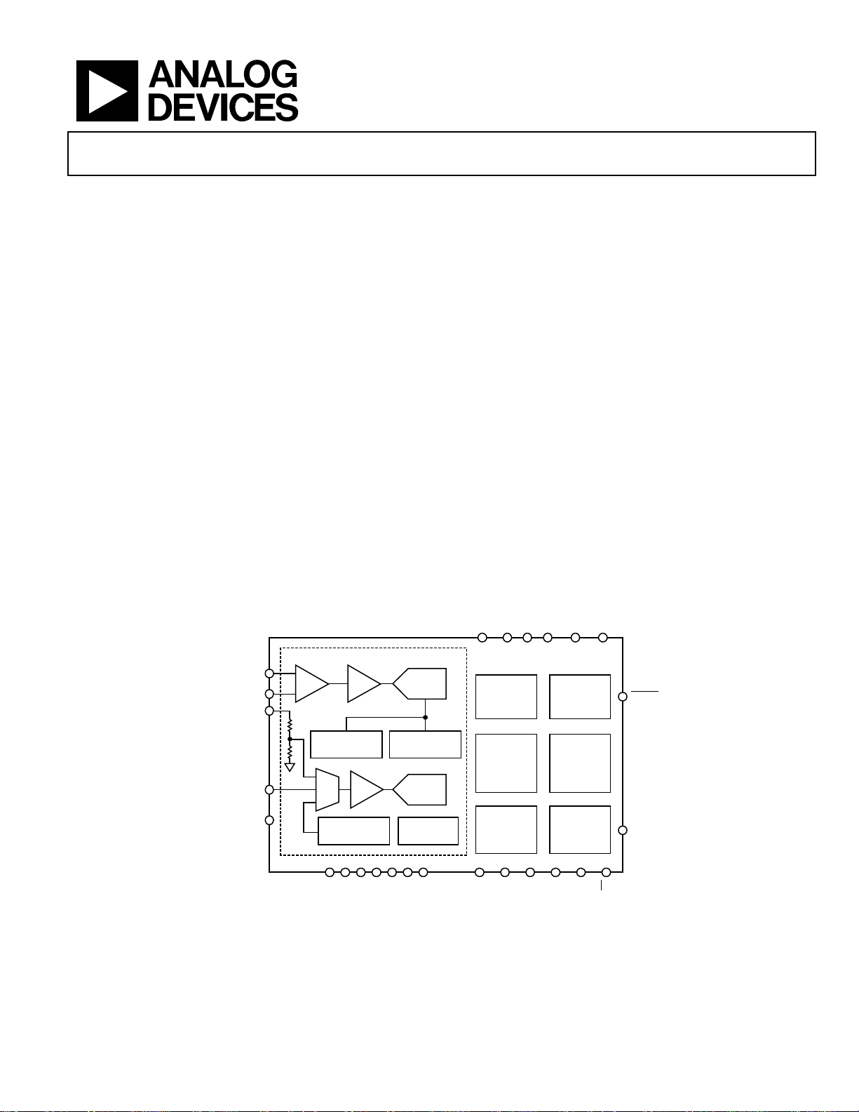
FUNCTIONAL BLOCK DIAGRAM
PRECISION ANAL OG ACQUISITION
IIN+
IIN–
VBAT
VTEMP
GND_SW
Rev. B
Information furnished by Analog Devices is believed to be accurate and reliable. However, no
responsibility is assumed by Analog Devices for its use, nor for any infringements of patents or other
rights of third parties that may result from its use. Specifications subject to change without notice. No
license is granted by implication or otherwise under any patent or patent rights of Analog Devices.
Trademarks and registered trademarks are the property of their respective owners.
BUF PGA
RESULT
ACCUMULATOR
MUX
BUF
TEMPERATURE
SENSOR
VDD
REG_AVDD
AGND
REG_DVDD
Σ-Δ ADC
DIGITAL
COMPARATOR
Σ-Δ ADC
PRECISION
REFERENCE
VSS
DGND
16-BIT
16-BIT
IO_VSS
Figure 1.
RTCK TDI TDO NTRST TMS
TC
ADuC7039
LDO
POR
20MHz
ARM7TDMI
MCU
1 × TIMER
WDT
W/U TIMER
GPIO_5
GPIO_4
One Technology Way, P.O. Box 9106, Norwood, MA 02062-9106, U.S.A.
Tel: 781.329.4700 www.analog.com
Fax: 781.461.3113 ©2010 Analog Devices, Inc. All rights reserved.
64KB FLASH
LOW POWER
ON-CHIP PLL
GPIO_3/ MOSI
MEMORY
4KB RAM
PRECISION
OSC
OSC
GPIO PORT
SPI PORT
LIN
GPIO_2/ MISO
GPIO_1/SCLK
RESET
LIN
GPIO_0/SS
08463-001
Page 2

ADuC7039
TABLE OF CONTENTS
Features .............................................................................................. 1
Applications ....................................................................................... 1
Functional Block Diagram .............................................................. 1
Revision History ............................................................................... 2
Specifications ..................................................................................... 3
Electrical Specifications ............................................................... 3
Timing Specifications .................................................................. 7
Absolute Maximum Ratings ............................................................ 8
ESD Caution .................................................................................. 8
Pin Configuration and Function Descriptions ............................. 9
Terminology .................................................................................... 11
Theory of Operation ...................................................................... 12
Overview of the ARM7TDMI-S Core ..................................... 12
Memory Organization ............................................................... 14
Reset ............................................................................................. 15
Flash/EE Memory ........................................................................... 16
Flash/EE MMR Interface ........................................................... 16
Flash/EE Memory Signature ..................................................... 20
Flash/EE Memory Security ....................................................... 21
Flash/EE Memory Reliability .................................................... 23
ADuC7039 Kernel ...................................................................... 23
Memory Mapped Registers (MMR) ............................................. 25
Complete MMR Listing ............................................................. 26
16-Bit, Sigma-Delta Analog-to-Digital Converters ................... 29
ADC Ground Switch .................................................................. 32
ADC Noise Performance Tables ............................................... 32
ADC MMR Interface ................................................................. 33
ADC Sinc3 Digital Filter Response .......................................... 42
ADC Modes of Operation ......................................................... 43
ADC Configuration ................................................................... 45
I-ADC Diagnostics ..................................................................... 46
REVISION HISTORY
8/10—Rev.A to Rev. B
Changes to Fast Temperature Conversion Mode Section ......... 46
Changes to Bit 4 Description (LINCON[6] Reference) in
Table 62 ............................................................................................ 86
Changes to Part Identification Section ........................................ 87
6/10—Rev. 0 to Rev. A
Added SAEJ2602 to Features Section ............................................ 1
Changes to Table 2 ............................................................................ 9
Power Supply Support Circuits ..................................................... 47
System Clocks ................................................................................. 48
Oscillators Calibration ............................................................... 53
Interrupt System ............................................................................. 58
Timers .............................................................................................. 60
Synchronization of TIMERS Across Asynchronous Clock
Domains ...................................................................................... 60
Programming the Timers .......................................................... 61
Timer0—General-Purpose Timer ........................................... 62
Timer1—Wake-Up Timer ......................................................... 64
Timer2—Watchdog Timer ........................................................ 66
General-Purpose Input/Output .................................................... 68
Serial Peripheral Interface (SPI) ................................................... 73
Master In, Slave Out (MISO) Pin ............................................. 73
Master Out, Slave In (MOSI) Pin ............................................. 73
Serial Clock I/O (SCLK) Pin ..................................................... 73
Slave Select (SS) Pin ................................................................... 73
SPI MMR Interface .................................................................... 73
High Voltage Peripheral Control Interface ................................. 77
Low Voltage Flag (LVF) ............................................................. 80
Handling HV Interface Interrupt and HV Communication 80
LIN (Local Interconnect Network) Interface.............................. 82
LIN Physical Interface ............................................................... 82
LIN Diagnostic ........................................................................... 83
LIN Communication ................................................................. 83
LIN MMRs .................................................................................. 83
Part Identification ........................................................................... 87
Recommended Schematic ............................................................. 89
Outline Dimensions ....................................................................... 90
Ordering Guide .......................................................................... 90
Changes to Bit 2 and Bit 1 Descriptions in Table 34 .................. 39
Changes to System Clocks Section ............................................... 49
Added Syncronization of Timers across Asynchronous Clock
Domains Section, Figure 23, and Figure 24 ................................ 60
Added Programming the Timers Section ................................... 61
Changes to Recommended Schematic Text ................................ 89
3/10—Revision 0: Initial Version
Rev. B | Page 2 of 92
Page 3

ADuC7039
SPECIFICATIONS
ELECTRICAL SPECIFICATIONS
VDD = 3.5 V to 18 V, V
+115°C, unless otherwise noted.
Table 1.
Parameter Test Conditions/Comments Min Typ Max Unit
ADC SPECIFICATIONS
Conversion Rate1 ADC normal operating mode 10 1000 Hz
ADC low power mode, chop on 10 650 Hz
Current Channel
No Missing Codes1 Valid for all ADC update rates and ADC modes 16 Bits
Integral Nonlinearity
Offset Error
Offset Error
Offset Error
Offset Error
Offset Error Drift
Offset Error Drift
Offset Error Drift
Total Gain Error
Low power mode −1 ±0.2 +1 %
Gain Drift
PGA Gain Mismatch Error ±0.1 %
Output Noise1 10 Hz update rate, gain = 512, chop enabled 100 150 nV rms
1 kHz update rate, gain = 512, ADCFLT = 0x0007 0.6 0.9 µV rms
1 kHz update rate, gain = 32, ADCFLT = 0x0007 0.8 1.2 µV rms
1 kHz update rate, gain = 8, ADCFLT = 0x8101 2.1 4.1 µV rms
1 kHz update rate, gain = 8, ADCFLT = 0x0007 1.6 2.4 µV rms
1 kHz update rate, gain = 4, ADCFLT = 0x0007 2.6 3.9 µV rms
ADC low power mode, 250Hz update rate, chop enable,
Voltage Channel8
No Missing Codes1 Valid at all ADC update rates 16 Bits
Integral Nonlinearity1 ±10 ±60 ppm of FSR
Offset Error
Offset Error
Offset Error Drift4 Chop off ±0.03 LSB/°C
Total Gain Error
Total Gain Error
Gain Drift
Output Noise
1 kHz update rate, ADCFLT = 0x0007 180 270 µV rms
Temperature Channel
No Missing Codes1 Valid at all ADC update rates 16 Bits
Integral Nonlinearity1 ±10 ±60 ppm of FSR
Offset Error
Offset Error
Offset Error Drift1 Chop off 0.03 LSB/°C
Total Gain Error
Gain Drift1 3 ppm/°C
Output Noise1 1 kHz update rate 7.5 11.25 µV rms
1, 2, 3
1, 3
1, 3
1, 3
1, 7
±3 ppm/°C
1, 3
1, 3
1, 7
Includes resistor mismatch drift ±3 ppm/°C
3, 10
1, 3
= 1.2 V internal reference, f
REF
1, 2
±10 ±60 ppm of FSR
Chop off, external short, after user system calibration,
= 20.48 MHz driven from on-chip precision oscillator, all specifications TA = −40°C to
CORE
−10 ±3 +10 LSB
1 LSB = (36.6/gain) µV
Chop on, external short, low power mode,
+250 ±50 −300 nV
MCU powered down
Chop on, external short, after user system calibration
0 3.0 µV
Tested at CD = 0, VDD = 18 V
Chop on, external short, after user system calibration
±0.5 µV
Tested at CD = 0, VDD = 4 V
1, 2, 4
Chop off, gains of 8 to 64, normal mode ±0.03 LSB/°C
1, 4
Chop off, valid for ADC gain of 512 ±30 nV/°C
1, 4
Chop on ±5 nV/°C
1, 3, 5 , 6
Factory calibrated at a gain of 4; normal mode −0.5 ±0.1 +0.5 %
0.6 0.9 µV rms
gain = 512
Chop off, 1 LSB = 439.5 µV, after two point calibration −10 ±1 +10 LSB
Chop on, after two point calibration −1 ±0.3 +1 LSB
1, 3, 5, 6
Includes resistor mismatch −0.25 ±0.06 +0.25 %
1, 3, 5, 6
Temperature range = −25°C to +65°C −0.15 ±0.03 +0.15 %
1, 9
10 Hz update rate, chop on 60 90 µV rms
Chop off, 1 LSB = 19.84 V (in unipolar mode) −10 ±3 +10 LSB
Chop on −5 +1 +5 LSB
1, 3, 10
VREF = (REG_AVDD, GND_SW)/2 −0.25 ±0.06 +0.25 %
Rev. B | Page 3 of 92
Page 4

ADuC7039
Parameter Test Conditions/Comments Min Typ Max Unit
ADC SPECIFICATIONS, ANALOG INPUT
Current Channel
Absolute Input Voltage Range1 Applies to both IIN+ and IIN− −200 +300 mV
Input Voltage Range
Gain = 4 ±300 mV
Gain = 8 ±150 mV
Gain = 32 ±37.5 mV
Gain = 512 ±2.3 mV
Input Leakage Current1 −3 +3 nA
Input Offset Current
Voltage Channel
Absolute Input Voltage Range1 Voltage ADC specifications are valid in this range 4 18 V
Input Voltage Range1 0 to 28.8 V
VBAT Input Current VBAT = 18 V 3 5.5 8 µA
Temperature Channel V
Absolute Input Voltage
14
Range
Input Voltage Range1 0 to V
VTEMP Input Current1 2.5 100 nA
VOLTAGE REFERENCE
Internal VREF 1.2 V
Power-Up Time1 0.5 ms
Initial Accuracy1 Measured at TA = 25°C −0.15 +0.15 %
Temperature Coefficient
Long-Term Stability16 100 ppm/1000 hr
ADC DIAGNOSTICS
VREF/136 Accuracy1 At any gain setting 8.4 9.4 mV
Voltage Attenuator Current Differential voltage increase on the attenuator when current is on 2.3 3.6 V
Source Accuracy1
RESISTIVE ATTENUATOR1
Divider Ratio 24
Resistor Mismatch Drift Included in the voltage channel total gain error ±3 ppm/°C
ADC GROUND SWITCH
Resistor to Ground 15 20 30 kΩ
TEMPERATURE SENSOR17 Uncalibrated
Accuracy MCU in power down or standby mode; TA = −40°C to +85°C −10 ±3 +10 °C
MCU in power down or standby mode; TA = −20°C to +60°C −8 ±2 +8 ºC
Calibrated − ADC2GN = 0x968A;
POWER-ON RESET (POR)1
POR Trip Level Refers to voltage at the VDD pin 2.85 3.0 3.15 V
POR Hysteresis 300 mV
Reset Timeout from POR 20 ms
LOW VOLTAGE FLAG(LVF)
LVF Level Refers to voltage at the VDD pin 1.9 2.1 2.3 V
WATCHDOG TIMER (WDT)
Timeout Period1 32 kHz clock, 256 prescale 0.008 524 Seconds
Timeout Step Size 7.8 ms
FLASH/EE MEMORY1
Endurance18 10,000 Cycles
Data Retention19 20 Years
DIGITAL INPUTS1 All digital inputs except NTRST
Input Leakage Current Input (high) = REG_DVDD ±1 ±10 µA
Input Pull-Up Current1 Input (low) = 0 V 10 20 80 µA
Input Capacitance1 10 pF
Input Leakage Current NTRST only; input (low) = 0 V ±1 ±10 µA
Input Pull-Down Current NTRST only; input (high) = REG_DVDD 30 55 100 µA
11, 12
1, 13
0.5 1.5 nA
= (REG_AVDD, GND_SW)/2
REF
100 1300 mV
V
REF
1, 15
−20 ±5 +20 ppm/°C
−4 ±2 +4 °C
MCU in power down or standby mode
Rev. B | Page 4 of 92
Page 5

ADuC7039
Parameter Test Conditions/Comments Min Typ Max Unit
LOGIC INPUTS1 All logic inputs
Input Low Voltage (VINL) 0.4 V
Input High Voltage (VINH) 2.0 V
ON-CHIP OSCILLATORS
Low Power Oscillator 128 kHz
Accuracy After user calibration at nominal supply and room
temperature; includes drift data from 1000 hr life-test
Precision Oscillator 128 kHz
Accuracy After run time calibration −1 +1 %
MCU CLOCK RATE1 10.24 MHz
MCU START-UP TIME1
At Power-On Includes kernel power-on execution time 25 ms
After Reset Event Includes kernel power-on execution time 5 ms
From MCU Power-Down Oscillator running 2 ms
Internal PLL Lock Time 1 ms
LIN I/O GENERAL
Baud Rate 1000 20,000 Bits/sec
VDD Supply voltage range for which the LIN interface is functional 7 18 V
Input Capacitance1 5.5 pF
LIN Comparator Response Time1 Using 22 Ω resistor 38 90 µs
LIN DC PARAMETERS
I
Current limit for driver when LIN bus is in dominant state;
LIN DOM MAX
VBAT = VBAT (maximum)
1
I
LIN_PAS_REC
I
LIN_PAS_DOM
I
LIN_NO_GND
I
BUS_NO_BAT
V
V
V
V
V
Driver off; 7.0 V < V
1
Input leakage, V
1, 20
Control unit disconnected from ground, GND = VDD;
1
VBAT disconnected, VDD = GND, 0 V < V
1
LIN receiver dominant state, VDD > 7.0 V 0.4 VDD V
LIN_DOM
1
LIN receiver recessive state, VDD > 7.0 V 0.6 VDD V
LIN_REC
1
LIN receiver center voltage, VDD > 7.0 V 0.475 VDD 0.5 VDD 0.525 VDD V
LIN_CNT
1
LIN receiver hysteresis voltage 0.175 VDD V
HYS
LIN_DOM_DRV_LOSUP
1
LIN dominant output voltage; VDD = 7.0 V
0 V < V
< 18 V; VBAT = 12 V
LIN
< 18 V; VDD = V
BUS
= 0 V −1 mA
LIN
− 0.7 V 20 µA
LIN
< 18 V 100 µA
BUS
RL 500 Ω 1.2 V
RL 1000 Ω 0.6 V
V
LIN_DOM_DRV_HISUP
1
LIN dominant output voltage; VDD = 18 V
RL 500 Ω 2 V
RL 1000 Ω 0.8 V
V
LIN_RECESSIVE
1
LIN recessive output voltage 0.8 VDD V
VBAT Shift20 0 0.115 VDD V
GND Shift20 0 0.115 VDD V
R
Slave termination resistance 20 30 47 kΩ
SLAVE
SERIAL DIODE
20
Voltage drop at the serial diode, D
0.4 0.7 1 V
Ser_Int
V
LIN AC PARAMETERS1 Bus load conditions (CBUS||RBUS):
1 nF||1 kΩ; 6.8 nF||660 Ω; 10 nF||500 Ω
D1 Duty Cycle 1 0.396
TH
TH
V
D1 = t
= 0.744 × VBAT
REC(MAX)
= 0.581 × VBAT
DOM(MAX)
= 7.0 V … 18 V; t
SUP
BUS_REC(MIN)
= 50 µs
BIT
/(2 × t
)
BIT
D2 Duty Cycle 2 0.581
TH
TH
V
D2 = t
= 0.284 × VBAT
REC(MIN)
= 0.422 × VBAT
DOM(MIN)
= 7.0 V … 18 V; t
SUP
BUS_REC(MAX)
= 50 µs
BIT
/(2 × t
)
BIT
−3 +3 %
40 200 mA
−1 +1 mA
Rev. B | Page 5 of 92
Page 6

ADuC7039
Parameter Test Conditions/Comments Min Typ Max Unit
1, 20
D3
TH
TH
V
t
D3 = t
1, 20
D4
TH
TH
V
t
D4 = t
1, 20
t
Propagation delay of receiver 6 μs
RX_PDR
1, 20
t
Symmetry of receiver propagation delay rising edge,
RX_SYM
PACKAGE THERMAL SPECIFICATIONS
Thermal Impedance (θJA)21 32-lead CSP, stacked die 32 °C/W
POWER REQUIREMENTS1
Power Supply Voltages
VDD (Battery Supply) 3.5 18 V
REG_DVDD, REG_AVDD22 2.45 2.6 2.75 V
Power Consumption
IDD (MCU Normal Mode)23 ADC off (20.48 MHz) 10 20 mA
ADC off (10.24 MHz) 7.5 16 mA
IDD (MCU Powered Down)1 ADC low power mode, measured over an ambient
IDD (MCU Powered Down)1 Precision oscillator turned off, ADC off
Average current, measured with wake-up and watchdog
Average current, measured with wake-up and watchdog
IDD (Current ADC) 1.7 mA
IDD (Voltage/Temperature ADC) 0.5 mA
IDD (Precision Oscillator) 400 μA
1
Not guaranteed by production test but by design and/or characterization data at production release.
2
Valid for current ADC gain setting of PGA up to 64.
3
These numbers include temperature drift.
4
The offset error drift is included in the offset error. This typical specification is an indicator of the offset error due to temperature drift. This typical value is the mean of
the temperature drift characterization data distribution.
5
Includes internal reference temperature drift.
6
User system calibration removes this error at a given temperature and at a given gain on the current channel.
7
The gain drift is included in the total gain error. This typical specification is an indicator of the gain error due to temperature drift. This typical value is the mean of the
temperature drift characterization data distribution.
8
Voltage channel specifications include resistive attenuator input stage.
9
RMS noise is referred to voltage attenuator input; for example, at f
input referred noise figures.
10
Valid after an initial self calibration.
11
It is possible to extend the ADC input range by up to 10% by modifying the factory set value of the gain calibration register or using system calibration. This approach
can also be used to reduce the ADC input range (LSB size).
12
In ADC low power mode, the input range is fixed at ±2.34375 mV.
13
Valid for a differential input less than 10 mV.
14
The absolute value of the voltage of VTEMP and GND_SW must be 100mV minimum, for accurate operation of the T-ADC.
15
Measured using box method.
16
The long-term stability specification is noncumulative. The drift in subsequent 1000 hour periods is significantly lower than in the first 1000 hour period.
17
Die temperature.
18
Endurance is qualified to 10,000 cycles, as per JEDEC Std. 22 Method A117 and measured at −40°C, +25°C, and +125°C. Typical endurance at 25°C is 170,000 cycles.
19
Retention lifetime equivalent at junction temperature (TJ) = 85°C, as per JEDEC Std. 22 Method A117. Retention lifetime derates with junction temperature.
20
These numbers are not production tested but are supported by LIN compliance testing.
21
Thermal impedance can be used to calculate the thermal gradient from ambient to die temperature.
22
Internal regulated supply available at REG_DVDD (I
23
Typical additional supply current consumed during Flash/EE memory program and erase cycles is 7 mA and 5 mA, respectively.
= 0.778 × VBAT 0.417
REC(MAX)
= 0.616 × VBAT
DOM(MAX)
= 7.0 V ... 18 V
DD
= 96 μs
BIT
/(2 × t
BUS_REC(MIN)
= 0.389 × VBAT 0.590
REC(min)
= 0.251 × VBAT
DOM(min)
= 7.0 V … 18 V
DD
= 96 μs
BIT
BUS_REC(MAX)
)
BIT
/(2 × t
)
BIT
−2 +2 μs
with respect to falling edge (t
RX_SYM
= t
RF_PDR
− t
RX_PDF
)
750 1000 μA
temperature range of T
= −10°C to +40°C, continuous ADC
A
conversion
95 300 μA
timers clocked from low power oscillator (−40°C to +85°C)
95 175 μA
timers clocked from low power oscillator over an ambient
temperature range of −10°C to +40°C
= 1 kHz, typical rms noise at the ADC input is 7.5 μV, scaled by the attenuator (24) yields these
ADC
= 5 mA) and REG_AVDD (I
SOURCE
SOURCE
=1 mA).
Rev. B | Page 6 of 92
Page 7
ADuC7039
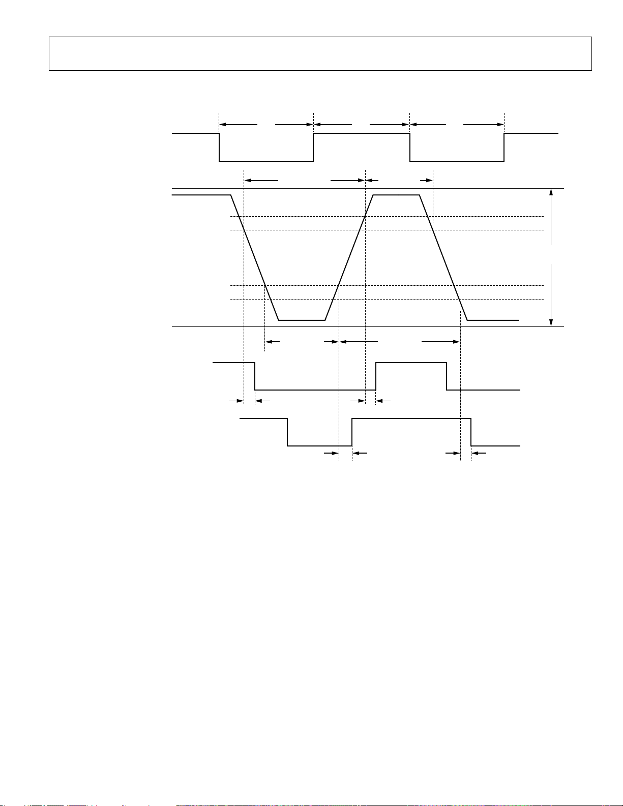
TIMING SPECIFICATIONS
LIN Timing Specifications
TRANSMIT
INPUT TO
TRANSMITTING
NODE
V
(TRANSCEIVER SUPPLY
OF TRANSMIT TING NODE)
SUP
RxD
(OUTPUT O F RECEIVING NODE 1)
RECESSIVE
DOMINANT
TH
REC (MAX)
TH
DOM (MAX)
TH
REC (MIN)
TH
DOM (MI N)
t
BIT
t
LIN_DO M (MAX )
t
LIN_DO M (MI N)
t
RX_PDF
t
BIT
t
LIN_REC ( MIN)
t
LIN_REC ( MAX)
t
RX_PDR
t
BIT
THRESHOLDS OF
RECEIVING NO DE 1
THRESHOLDS OF
RECEIVING NO DE 2
LIN
BUS
(OUTPUT O F RECEIVING NODE 2)
RxD
t
RX_PDR
Figure 2. LIN 2.1 Timing Specification
t
RX_PDF
08463-002
Rev. B | Page 7 of 92
Page 8
ADuC7039
ABSOLUTE MAXIMUM RATINGS
TA = −40°C to +115°C, unless otherwise noted.
Table 2.
Parameter Rating
AGND to DGND to VSS to IO_VSS −0.3 V to +0.3 V
VBAT to AGND −22 V to +40 V
VDD to VSS −0.3 V to +40 V
LIN to IO_VSS −16 V to +40 V
LIN Short-Circuit Current1 200 mA
Digital I/O Voltage to DGND −0.3 V to REG_DVDD + 0.3 V
ADC Inputs to AGND −0.3 V to REG_AVDD + 0.3 V
ESD (HBM) Rating
HBM-ADI0082 (Based on
ANSI/ESD STM5.1-2007); All Pins
Except LIN and VBAT
LIN and VBAT ±6 kV
IEC61000-4-2 for LIN and VBAT ±7 kV
Storage Temperature 150°C
Junction Temperature
Transient 150°C
Continuous 130°C
Lead Temperature
Soldering Reflow (15 sec) 260°C
1
200 mA can be sustained on the LIN pin for 2 seconds. The active internal
short circuit protection HVCFG[1] = 0 is required to be enabled on this
device during LIN operation and is the default operation. This disconnects
the LIN pin, if a short circuit event occurs, after the specified maximum
period of 90 µs.
2.5 kV
Stresses above those listed under Absolute Maximum Ratings
may cause permanent damage to the device. This is a stress
rating only; functional operation of the device at these or any
other conditions above those indicated in the operational
section of this specification is not implied. Exposure to absolute
maximum rating conditions for extended periods may affect
device reliability.
ESD CAUTION
Rev. B | Page 8 of 92
Page 9
ADuC7039
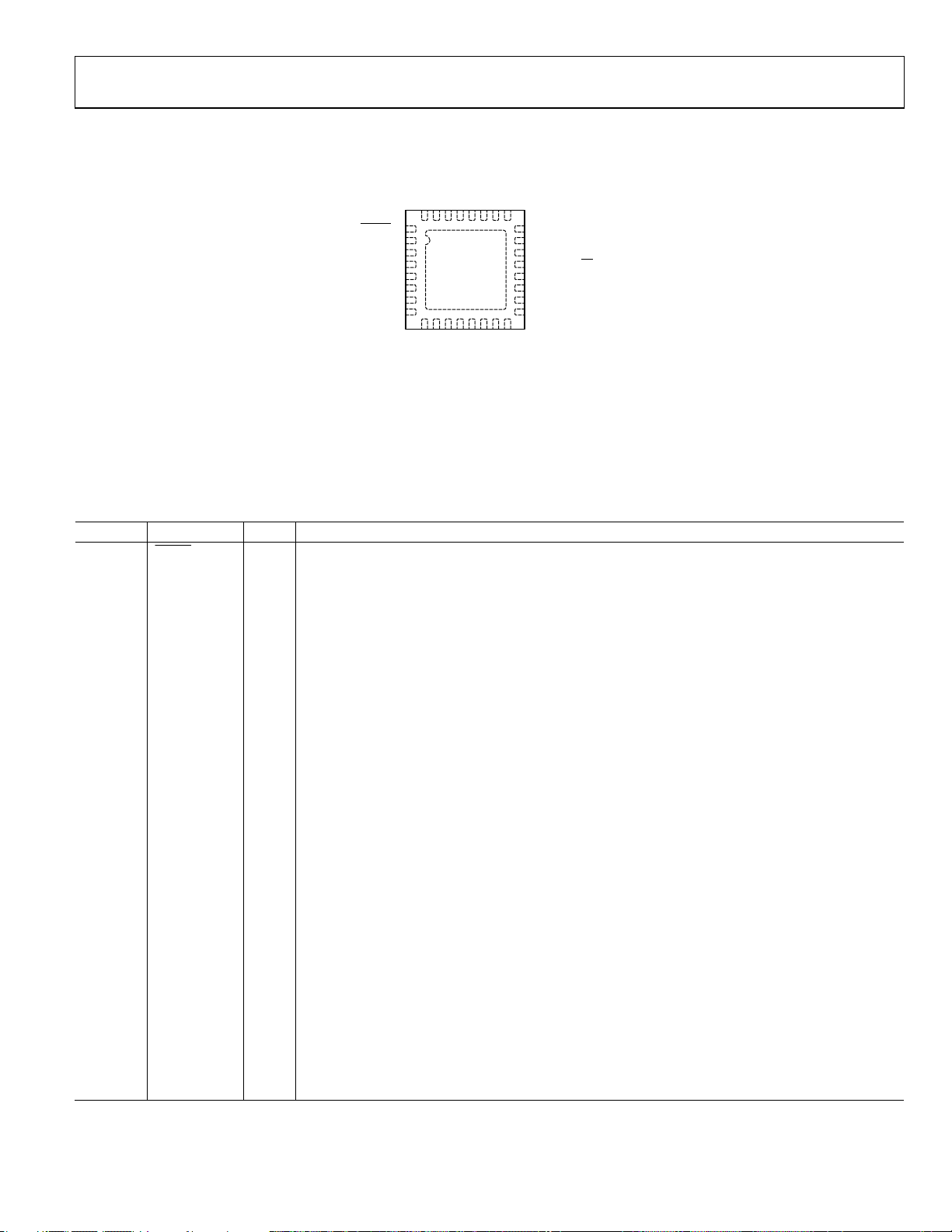
PIN CONFIGURATION AND FUNCTION DESCRIPTIONS
GPIO_5
VSS
IO_VSS
LIN
VBAT
TOP VIEW
IIN+
AGND
IIN–
VDDNCGPIO_4
AGND
AGND
25
REG_AVDD
24
23
GPIO_2/ MISO
GPIO_1/ SCLK
22
GPIO_0/ SS
21
20
DGND
19
REG_DVDD
18
REG_DVDD
17
8463-003
32313029282726
RESET
1 GPIO_3/MOSI
2
TDO
TCK
3
TMS
TDI
NTRST
RTCK
NC
NOTES:
1. FOR DETAILS ON NC PINS, SEE T HE PIN FUNCT ION
DESCRIPTIO NS TABLE.
2. EPAD IS INTERNALLY CO NNECTED TO DGND.
ADuC7039
4
5
(Not to Scale)
6
7
8REG_AVDD
9
10111213141516
VTEMP
GND_SW
Figure 3. Pin Configuration
Table 3. Pin Function Descriptions
Pin No. Mnemonic Type1 Description
1
RESET
I Reset Input Pin. Active low. This pin has an internal, weak, pull-up resistor to REG_DVDD. When not in
use, this pin can be left unconnected. For added security and robustness, it is recommended that this
pin be strapped via a resistor to REG_DVDD.
2 TDO O
JTAG Test Data Output. This data output pin is one of the standard 6-pin JTAG debug ports on the
part. TDO is an output pin only. At power-on, this output is disabled and pulled high via an internal,
weak, pull-up resistor. This pin can be left unconnected when not in use.
3 TCK I
JTAG Test Clock. This clock input pin is one of the standard 6-pin JTAG debug ports on the part. TCK
is an input pin only and has an internal, weak, pull-up resistor. This pin can be left unconnected when
not in use.
4 TMS I
JTAG Test Mode Select. This mode select input pin is one of the standard 6-pin JTAG debug ports on
the part. TMS is an input pin only and has an internal, weak, pull-up resistor. This pin can be left
unconnected when not in use.
5 TDI I
JTAG Test Data Input. This data input pin is one of the standard 6-pin JTAG debug ports on the part.
TDI is an input pin only and has an internal, weak, pull-up resistor. This pin can be left unconnected
when not in use.
6 NTRST I
JTAG Test Reset. This reset input pin is one of the standard 6-pin JTAG debug ports on the part.
NTRST is an input pin only and has an internal, weak, pull-down resistor. This pin can be left unconnected when not in use. NTRST is also monitored by the on-chip kernel to enable LIN boot load mode.
7 RTCK O
JTAG Return Test Clock. This output pin is used to adjust the JTAG clock speed to the highest possible
rate of the ADuC7039.
8 NC No Connect. This pin is internally connected; therefore, do not externally connect this pin.
9 GND_SW I
Switch to Internal Analog Ground Reference. This pin is the negative input for the external temperature
channel and external reference. If this input is not used, connect it directly to the AGND system ground.
10 VTEMP I External Pin for NTC/PTC Temperature Measurement.
11, 14, 15 AGND S Ground Reference for On-Chip Precision Analog Circuits.
12 IIN+ I Positive Differential Input for Current Channel.
13 IIN− I Negative Differential Input for Current Channel.
16, 17 REG_AVDD S
Nominal 2.6 V analog Output from On-Chip Regulator. Pin 16 and Pin 17 must be connected together
to a capacitor to ground.
18, 19 REG_DVDD S
Nominal 2.6 V digital Output from On-Chip Regulator. Pin 18 and Pin 19 must be connected together
to capacitors to ground.
20 DGND S Ground Reference for On-Chip Digital Circuits.
Rev. B | Page 9 of 92
Page 10

ADuC7039
Pin No. Mnemonic Type1 Description
21
GPIO_0/SS
22 GPIO_1/SCLK I/O
23 GPIO_2/MISO I/O
24 GPIO_3/MOSI I/O
25 GPIO_4 I/O
26 NC
27 VDD S Battery Power Supply to On-Chip Regulator.
28 VBAT I Battery Voltage Input to Resistor Divider.
29 LIN I/O LIN Serial Interface Input/Output Pin.
30 IO_VSS S Ground Reference for LIN Pin.
31 VSS S Ground Reference. This is the ground reference for the internal voltage regulators.
32 GPIO_5 I/O
EPAD EPAD The exposed pad is internally connected to DGND.
1
I = input, O = output, S = supply.
I/O General-Purpose Digital I/O 0, or SPI Interface. By default, this pin is configured as an input. The
pin has an internal, weak, pull-up resistor and, when not in use, can be left unconnected. This
multifunction pin can be configured in one of two states, namely
General-Purpose Digital I/O 0.
SPI interface, slave select input.
General-Purpose Digital I/O 1 or SPI Interface. By default, this pin is configured as an input. The pin
has an internal, weak, pull-up resistor and, when not in use, can be left unconnected. This
multifunction pin can be configured in one of two states, namely
General-Purpose Digital I/O 1.
SPI interface, serial clock input.
General-Purpose Digital I/O 2 or SPI Interface. By default, this pin is configured as an input. The pin
has an internal, weak, pull-up resistor and, when not in use, can be left unconnected. This
multifunction pin can be configured in one of two states, namely
General-Purpose Digital I/O 2.
SPI interface, master input/slave output pin.
General-Purpose Digital I/O 3 or SPI Interface. By default, this pin is configured as an input. The pin
has an internal, weak, pull-up resistor and, when not in use, can be left unconnected. This
multifunction pin can be configured in one of two states, namely
General-Purpose Digital I/O 3.
SPI interface, master output/slave input pin.
General-Purpose I/O 4. By default, this pin is configured as an input. The pin has an internal, weak,
pull-up resistor and when not in use, can be left unconnected.
No Connect. This pin is not internally connected, but is reserved for possible future use. Therefore,
do not externally connect this pin.
General-Purpose I/O 5. By default, this pin is configured as an input. The pin has an internal, weak,
pull-up resistor and when not in use, can be left unconnected.
Rev. B | Page 10 of 92
Page 11

ADuC7039
TERMINOLOGY
Conversion Rate
The conversion rate specifies the rate at which an output result
is available from the ADC, after the ADC has settled.
The sigma-delta (Σ-) conversion techniques used on this part
mean that while the ADC front-end signal is oversampled at a
relatively high sample rate, a subsequent digital filter is used to
decimate the output giving a valid 16-bit data conversion result
at output rates from 1 Hz to 1 kHz.
Note that when software switches from one input to another
(on the same ADC), the digital filter must first be cleared and
then allowed to average a new result. Depending on the configuration of the ADC and the type of filter, this can require
multiple conversion cycles.
Integral Nonlinearity (INL)
INL is the maximum deviation of any code from a straight
line passing through the endpoints of the transfer function.
The endpoints of the transfer function are zero scale, a point
½ LSB below the first code transition, and full scale, a point ½
LSB above the last code transition (111 . . . 110 to 111 . . . 111).
The error is expressed as a percentage of full scale.
No Missing Codes
No missing codes is a measure of the differential nonlinearity
of the ADC. The error is expressed in bits and specifies the
number of codes (ADC results) as 2
N
bits, where N = no
missing codes, guaranteed to occur through the full ADC
input range.
Offset Error
Offset error is the deviation of the first code transition ADC
input voltage from the ideal first code transition.
Offset Error Drift
Offset error drift is the variation in absolute offset error with
respect to temperature. This error is expressed as LSB/°C
or nV/°C.
Gain Error
Gain error is a measure of the span error of the ADC. It is a
measure of the difference between the measured and the ideal
span between any two points in the transfer function.
Output Noise
The output noise is specified as the standard deviation (or 1 × Σ)
of ADC output codes distribution collected when the ADC
input voltage is at a dc voltage. It is expressed as µV or nV rms.
The output, or rms noise, can be used to calculate the effective
resolution of the ADC as defined by the following equation:
Effective Resolution = log
(Full-Scale Range/rms Noise) bits
2
The peak-to-peak noise is defined as the deviation of codes that
fall within 6.6 × Σ of the distribution of ADC output codes collected when the ADC input voltage is at dc. The peak-to-peak
noise is, therefore, calculated as 6.6 × the rms noise.
The peak-to-peak noise can be used to calculate the ADC
(noise free, code) resolution for which there is no code flicker
within a 6.6 × Σ limit as defined by the following equation:
Noise Free Code Resolution = log
(Full-Scale Range/Peak-
2
to-Peak Noise) bits
Table 4. Data Sheet Acronyms
Acronym Definition
ADC Analog-to-digital converter
ARM Advanced RISC machine
JTAG Joint test action group
LIN Local interconnect network
LSB Least significant byte/bit
MCU Microcontroller
MMR Memory mapped register
MSB Most significant byte/bit
OTP One time programmable
PID Protected identifier
POR Power-on reset
rms Root mean square
Rev. B | Page 11 of 92
Page 12

ADuC7039
THEORY OF OPERATION
The ADuC7039 is a complete system solution for battery monitoring in 12 V automotive applications. This device integrates
all of the required features to precisely and intelligently monitor,
process, and diagnose 12 V battery parameters including battery
current, voltage, and temperature over a wide range of operating conditions.
Minimizing external system components, the device is powered
directly from the 12 V battery. An on-chip, low dropout regulator generates the supply voltage for two integrated, 16-bit, Σ-
ADCs. The ADCs precisely measure battery current, voltage,
and temperature to characterize the state of health and charge
of the car battery.
A Flash/EE memory-based ARM7™ microcontroller (MCU) is
also integrated on-chip. It is used to both preprocess the acquired
battery variables and to manage communications from the
ADuC7039 to the main electronic control unit (ECU) via a local
interconnect network (LIN) interface that is integrated on-chip.
The MCU can be configured to operate in normal or flexible
power saving modes of operation.
In its normal operating mode, the MCU is clocked indirectly
from an on-chip oscillator via the phase-locked loop (PLL) at
a maximum clock rate of 10.24 MHz. In its power saving operating modes, the MCU can be totally powered down, waking
up only in response to the wake-up timer, a POR, or a LIN
communication event.
The ADC can be configured to operate in a normal (full power)
mode of operation, interrupting the MCU after various sample
conversion events.
On-chip factory firmware supports in-circuit Flash/EE reprogramming via the LIN or JTAG serial interface ports, and
nonintrusive emulation is also supported via the JTAG interface.
These features are incorporated into a low cost QuickStart™
development system supporting the ADuC7039.
The ADuC7039 operates directly from the 12 V battery supply
and is fully specified over a temperature range of −40°C to
+115°C. The ADuC7039 is functional, but with degraded
performance, at temperatures from 115°C to 125°C.
OVERVIEW OF THE ARM7TDMI-S CORE
The ARM7 core is a 32-bit, reduced instruction set computer
(RISC), developed by ARM® Ltd. The ARM7TDMI-S is a von
Neumann-based architecture, meaning that it uses a single
32-bit bus for instruction and data. The length of the data
can be 8, 16, or 32 bits, and the length of the instruction word
is either 16 bits or 32 bits, depending on the mode in which
the core is operating.
The ARM7TDMI-S is an ARM7 core with four additional
features, as listed in Tabl e 5.
Table 5. ARM7TDMI-S
Feature Description
T Support for the Thumb® (16-bit) instruction set
D Support for debug
M Enhanced multiplier
I
Includes the EmbeddedICE™ module to support
embedded system debugging
Thumb Mode (T)
An ARM instruction is 32 bits long. The ARM7TDMI-S processor supports a second instruction set compressed into 16 bits,
the Thumb instruction set. Faster code execution from 16-bit
memory and greater code density can be achieved by using the
Thumb instruction set, making the ARM7TDMI-S core
particularly suited for embedded applications.
However, the Thumb mode has three limitations.
• Relative to ARM, the Thumb code usually requires more
instructions to perform that same task. Therefore, ARM
code is best for maximizing the performance of timecritical code in most applications.
• The Thumb instruction set does not include some
instructions that are needed for exception handling,
so ARM code can be required for exception handling.
• When an interrupt occurs, the core vectors to the interrupt
location in memory and executes the code present at that
address. The first command is required to be in ARM code.
Multiplier (M)
The ARM7TDMI-S instruction set includes an enhanced
multiplier, with four extra instructions to perform 32-bit by
32-bit multiplication with a 64-bit result, and 32-bit by 32-bit
multiplication-accumulation (MAC) with a 64-bit result.
EmbeddedICE (I)
The EmbeddedICE module provides integrated on-chip
debug support for the ARM7TDMI-S. The EmbeddedICE
module contains the breakpoint and watchpoint registers
that allow nonintrusive user code debugging. These registers
are controlled through the JTAG test port. When a breakpoint
or watchpoint is encountered, the processor halts and enters
the debug state. Once in a debug state, the processor registers
can be interrogated, as can the Flash/EE, SRAM, and memory
mapped registers.
Rev. B | Page 12 of 92
Page 13
ADuC7039
ARM7 Exceptions
The ARM7 supports five types of exceptions, with a privileged
processing mode associated with each type. The five types of
exceptions are as follows:
• Normal interrupt or IRQ. This is provided to service
general-purpose interrupt handling of internal and
external events.
• Fast interrupt or FIQ. This is provided to service data
transfer or a communication channel with low latency.
FIQ has priority over IRQ.
• Memory abort (prefetch and data).
• Attempted execution of an undefined instruction.
• Software interrupt (SWI) instruction that can be used
to make a call to an operating system.
Typically, the programmer defines interrupts as IRQ, but
for higher priority interrupts, the programmer can define
interrupts as the FIQ type.
The priority of these exceptions and the vector addresses are
listed in Table 6 .
Table 6. Exception Priorities and Vector Addresses
Priority Exception Address
1 Hardware reset 0x00
2 Memory abort (data) 0x10
3 FIQ 0x1C
4 IRQ 0x18
5 Memory abort (prefetch) 0x0C
6 Software interrupt1 0x08
6 Undefined instruction1 0x04
1
A software interrupt and an undefined instruction exception have the same
priority and are mutually exclusive.
ARM Registers
The ARM7TDMI-S has 16 standard registers. R0 to R12 are
used for data manipulation, R13 is the stack pointer, R14 is the
link register, and R15 is the program counter that indicates the
instruction currently being executed. The link register contains
the address from which the user has branched (if the branch
and link command was used) or the command during which
an exception occurred.
The stack pointer contains the current location of the stack. As
a general rule, on an ARM7TDMI-S, the stack starts at the top
of the available RAM area and descends using the area as
required. A separate stack is defined for each of the exceptions.
The size of each stack is user configurable and is dependent on
the target application. On the ADuC7039, the stack begins at
0x00040FFC and descends. When programming using high
level languages, such as C, it is necessary to ensure that the stack
does not over-flow. This is dependent on the performance of
the compiler that is used.
When an exception occurs, some of the standard registers are
replaced with registers specific to the exception mode. All
exception modes have replacement banked registers for the
Rev. B | Page 13 of 92
stack pointer (R13) and the link register (R14) as represented
in Figure 4. The FIQ mode has more registers (R8 to R12)
supporting faster interrupt processing. With the increased
number of noncritical registers, the interrupt can be processed
without the need to save or restore these registers, thereby
reducing the response time of the interrupt handling process.
More information relative to the programmer’s model and the
ARM7TDMI-S core architecture can be found in ARM7TDMI-S
technical and ARM architecture manuals available directly from
ARM Ltd.
R13_ABT
R14_ABT
ABORT
MODE
USABLE IN USER MODE
SYSTEM MODES ONLY
IRQ
R13_UND
R14_UND
SPSR_UND
UNDEFINED
MODE
R13_IRQ
R14_IRQ
SPSR_IRQ
MODE
R10
R11
R12
R13
R14
R15 (PC)
CPSR
USER MODE
R0
R1
R2
R3
R4
R5
R6
R7
R8
R9
R8_FIQ
R9_FIQ
R10_FIQ
R11_FIQ
R12_FIQ
R13_FIQ
R14_FIQ
SPSR_FIQ
R13_SVC
R14_SVC
SVC
MODE
SPSR_ABT
SPSR_SVC
FIQ
MODE
Figure 4. Register Organization
Interrupt Latency
The worst-case latency for an FIQ consists of the longest time
the request can take to pass through the synchronizer, and the
time for the longest instruction to complete (the longest instruction is an LDM that loads all the registers including the PC),
plus the time for the data abort entry and the time for FIQ
entry. At the end of this time, the ARM7TDMI-S is executing
the instruction at 0x1C (FIQ interrupt vector address). The
maximum total time is 50 processor cycles, or just under 5 s
in a system using a continuous 10.24 MHz processor clock. The
maximum IRQ latency calculation is similar but must allow for
the fact that FIQ has higher priority and could delay entry into
the IRQ handling routine for an arbitrary length of time. This
time can be reduced to 42 cycles if the LDM command is not
used; some compilers have an option to compile without using
this command. Another option is to run the part in Thumb
mode where this is reduced to 22 cycles.
The minimum latency for FIQ or IRQ interrupts is five cycles.
This consists of the shortest time the request can take through
the synchronizer and the time to enter the exception mode.
Note that the ARM7TDMI-S initially (first instruction) runs
in ARM (32-bit) mode when an exception occurs. The user
can immediately switch from ARM mode to Thumb mode
if required, for example, when executing interrupt service
routines.
08463-004
Page 14

ADuC7039
MEMORY ORGANIZATION
The ARM7, a von Neumann architecture, MCU core sees memory as a linear array of 2
the ADuC7039 maps this into four distinct user areas, namely: a
memory area that can be remapped, an SRAM area, a Flash/EE
area, and a memory mapped register (MMR) area.
0xFFFF0000
0x00080000
0x00040000
0x00000000
Figure 5. ADuC7039 Memory Map, 64 kB Flash Option
• The first 64 kB of this memory space is used as an area into
which the on-chip Flash/EE or SRAM can be remapped.
• The ADuC7039 features a second 4 kB area at the top of
the memory map used to locate the MMRs, through which
all on-chip peripherals are configured and monitored.
• The ADuC7039 features an SRAM size of 4 kB.
• The ADuC7039 features 64 kB of on-chip Flash/EE
memory. However, 62 kB of on-chip Flash/EE memory are
available to the user. In addition, 2 kB are reserved for the
on-chip kernel.
32
byte locations. As shown in Figure 5,
RESERVED
0xFFFF0FFF
0x0008FFFF
0x0040FFF
0x0000F7FF
MMRs
RESERVED
FLASH/EE
RESERVED
SRAM
RESERVED
REMAPPABLE MEMORY SPACE
(FLASH/EE OR SRAM)
8463-005
SRAM
The ADuC7039 features 4 kB of SRAM, organized as 1024 × 32
bits, that is, 1024 words, which is located at 0x40000.
The RAM space can be used as data memory and also as a
volatile program space.
ARM code can run directly from SRAM at full clock speed
given that the SRAM array is configured as a 32-bit wide
memory array. SRAM is read/writeable in 8-, 16-, and 32-bit
segments.
Remap
The ARM exception vectors are all situated at the bottom
of the memory array, from Address 0x00000000 to Address
0x00000020.
By default, after a reset, the Flash/EE memory is logically mapped
to Address 0x00000000. It is possible to logically remap the
SRAM to Address 0x00000000. This is accomplished by setting
Bit 0 of the SYSMAP MMR located at 0xFFFF0220. To revert
Flash/EE to 0x00000000, Bit 0 of SYSMAP is cleared.
It is sometimes desirable to remap RAM to 0x00000000 to
execute code from SRAM while erasing a page of Flash/EE
memory.
Remap Operation
When a reset occurs on the ADuC7039, execution starts automatically in the factory programmed internal configuration
code. This so-called kernel is hidden and cannot be accessed
by user code. If the ADuC7039 is in normal mode, it executes
the power-on configuration routine of the kernel and then
jumps to the reset vector, Address 0x00000000, to execute the
user’s reset exception routine. Because the Flash/EE is mirrored
at the bottom of the memory array at reset, the reset routine
must always be written in Flash/EE.
Any access, either reading or writing, to an area not defined in
the memory map results in a data abort exception.
Memory Format
The ADuC7039 memory organization is configured in little
endian format: the least significant byte is located in the lowest
byte address, and the most significant byte in the highest byte
address.
BIT 31
BYTE 3
.
.
.
B
7
3
BYTE 2
BYTE 1
.
.
.
.
.
.
A
9
6
5
2
1
32 BITS
Figure 6. Little Endian Format
BYTE 0
.
.
.
8
4
0
BIT 0
0xFFFFFFFF
0x00000004
0x00000000
8463-007
Rev. B | Page 14 of 92
Page 15

ADuC7039
The remap command must be executed from the absolute
Flash/EE address, and not from the mirrored, remapped
segment of memory, because this may be replaced by SRAM. If
a remap operation is executed while operating code from
the mirrored location, prefetch/data aborts can occur, or the
user can observe abnormal program operation.
Any kind of reset logically remaps the Flash/EE memory to
the bottom of the memory array.
SYSMAP Register
Name: SYSMAP
RSTSTA Register
Name: RSTSTA
Address: 0xFFFF0230
Default Value: N/A
Access: Read/write
Function: This 8-bit register indicates the source of the
last reset event and can also be written by user
code to initiate a software reset.
Address: 0xFFFF0220
Default Value: Updated by the kernel
Access: Read/write
Function: This 8-bit register allows user code to remap
either RAM or Flash/EE space into the bottom
of the ARM memory space starting at Address
0x00000000.
Table 7. SYSMAP MMR Bit Designations
Bit Description
7 to 1
Reserved. These bits are reserved and should be written
as 0 by user code.
0 Remap bit.
This bit is set by the user to remap the SRAM to
0x00000000.
This bit is cleared automatically after reset to remap the
Flash/EE memory to 0x00000000.
RESET
There are four kinds of reset: external reset, power-on-reset,
watchdog reset, and software reset. The RSTSTA register
indicates the source of the last reset and can also be written
by user code to initiate a software reset event. The bits in this
register can be cleared to 0 by writing to the RSTCLR MMR at
0xFFFF0234. The bit designations in RSTCLR mirror those of
RSTSTA. These registers can be used during a reset exception
service routine to identify the source of the reset. The implications of all four kinds of reset event are tabulated in Ta ble 9.
RSTCLR Register
Name: RSTCLR
Address: 0xFFFF0234
Access: Write only
Function: This 8-bit write-only register clears the
corresponding bit in RSTSTA.
Table 8. RSTSTA/RSTCLR MMR Bit Designations
Bit Description
7 to 4 Not used. These bits are not used and always read as 0.
3 External reset.
This bit is set by hardware when an external reset occurs.
This bit is cleared by setting the corresponding bit in RSTCLR.
2 Software reset.
This bit is set by user code to generate a software reset.
This bit is cleared by setting the corresponding bit in RSTCLR.1
1 Watchdog timeout.
This bit is set by hardware when a watchdog timeout occurs.
This bit is cleared by setting the corresponding bit in RSTCLR.
0 Power-on reset.
This bit is set by hardware when a power-on-reset occurs.
This bit is cleared by setting the corresponding bit in RSTCLR.
1
If the software reset bit in RSTSTA is set, any write to RSTCLR that does not
clear this bit generates a software reset.
Table 9. Device Reset Implications
Impact
Reset External
RESET
POR Yes Yes Yes Yes Yes Yes Yes/No2 RSTSTA[0] = 1
Watchdog Yes Yes Yes Yes Yes No Yes RSTSTA[1] = 1
Software Yes Yes Yes Yes Yes No Yes RSTSTA[2] = 1
External Pin Yes Yes Yes Yes Yes No Yes RSTSTA[3] = 1
1
RAM is not valid in the case of a reset following LIN download.
2
The impact on RAM is dependent on the HVSTA[2] contents if LVF is enabled. When LVF is enabled using HVCFG[4], RAM has not been corrupted by the POR reset
mechanism if the LVF Status Bit HVSTA[2] is 1. See the Low Voltage Flag (LVF) section for more information.
Pins to Default
State
Kernel
Executed
Reset All External
MMRs (Excluding
RSTSTA)
Reset All HV
Indirect
Registers
Peripherals
Reset
Watchdog
Timer Reset
RAM
Valid1
RSTSTA (Status
After Reset Event)
Rev. B | Page 15 of 92
Page 16

ADuC7039
FLASH/EE MEMORY
The ADuC7039 incorporates Flash/EE memory technology
on chip to provide the user with nonvolatile, in-circuit
reprogrammable memory space.
Like EEPROM, flash memory can be programmed in-system
at a byte level, although it must first be erased, the erase being
performed in page blocks. Thus, flash memory is often and
more correctly referred to as Flash/EE memory.
Overall, Flash/EE memory represents a step closer to the ideal
memory device that includes nonvolatility, in-circuit programmability, high density, and low cost. Incorporated within the
ADuC7039, Flash/EE memory technology allows the user to
update program code space in-circuit, without the need to
replace one-time programmable (OTP) devices at remote
operating nodes.
The Flash/EE memory is physically located at 0x80000. Upon a
hard reset, it logically maps to 0x00000000. The factory default
contents of all Flash/EE memory locations is 0xFFFF. Flash/EE
can be read in 8-/16-/32-bit segments, and written in segments
of 16 bits. The Flash/EE is rated for 10,000 endurance cycles.
This rating is based on the number of times that each individual
byte is cycled, that is, erased and programmed. Implementing a
redundancy scheme in the software ensures a greater than
10,000-cycle endurance.
The user can also write data variables to the Flash/EE memory
during run-time code execution, for example, for storing
diagnostic battery parameter data.
The entire Flash/EE is available to the user as code and nonvolatile data memory. There is no distinction between data and
program, because ARM code shares the same space. The real
width of the Flash/EE memory is 16 bits, meaning that in ARM
mode (32-bit instruction), two accesses to the Flash/EE are
necessary for each instruction fetch. The ARM7TDMI-S
operates at a fixed 10.24 MHz clock frequency, but the Flash/EE
memory controller is operating at 20.48 MHz. This means that
the Flash/EE memory controller can transparently fetch the
second 16-bit half-word (part of the 32-bit ARM operation
code) within a single core clock period.
The page size of this Flash/EE memory is 512 bytes. Typically,
it takes the Flash/EE controller 20 ms to erase a page. To write a
16-bit word requires 50 s.
It is possible to write to a single, 16-bit location at most twice
between erases; that is, it is possible to walk bytes, not bits. If
a location is written to more than twice, then it is possible to
corrupt the contents of the Flash/EE page.
The Flash/EE memory can be programmed in-circuit, using a
serial download mode via the LIN interface or the integrated
JTAG port.
Serial Downloading (In-Circuit Programming)
The ADuC7039 facilitates code download via the LIN pin.
The protocol is documented in the AN-946 Application
Note, Flash/EE Memory Programming via LIN (Protocol 6).
JTAG Access
The ADuC7039 features an on-chip JTAG debug port to
facilitate code download and debug.
FLASH/EE MMR INTERFACE
Access to, and control of, the Flash/EE memory on the ADuC7039
is managed by an on-chip memory controller. The controller
manages the Flash/EE memory as a single block of 64 kB.
Note that if executing from Flash/EE memory, the MCU core
is halted until the command is completed. User software must
ensure that the Flash/EE controller has completed any erase
or write cycle before the PLL is powered down. If the PLL is
powered down before an erase or write cycle is completed, the
Flash/EE page can be corrupted. User code, LIN, and JTAG
programming use the Flash/EE control interface, consisting
of the following MMRs:
• FEESTA: read-only register, reflects the status of the
Flash/EE control interface.
• FEEMOD: sets the operating mode of the Flash/EE control
interface.
• FEECON: 8-bit command register. The commands are
interpreted as described in Ta bl e 10 .
• FEEDAT: 16-bit data register.
• FEEADR: 16-bit address register.
• FEESIG: holds the 24-bit code signature as a result of the
signature command being initiated.
• FEEHID: protection MMR. Controls read and write
protection of the Flash/EE memory code space. If
previously configured via the FEEPRO register, FEEHID
can require a software key to enable access.
• FEEPRO: a buffer of the FEEHID register that stores the
FEEHID value, thus, it automatically downloads to the
FEEHID registers on subsequent reset and power-on
events.
The following sections provide detailed descriptions of the bit
designations for each of the Flash/EE control MMRs.
Rev. B | Page 16 of 92
Page 17

ADuC7039
FEECON Register
Name: FEECON
Address: 0xFFFF0E08
Default Value: 0x07
Access: Read/write
Function: This 8-bit register is written by user code to control the operating modes of the Flash/EE memory controller.
Table 10. Command Codes in FEECON
Code Command Description
0x001 Reserved Reserved; this command should not be written by user code.
0x011 Single read Load FEEDAT with the 16-bit data indexed by FEEADR.
0x021 Single write Write FEEDAT at the address indexed by FEEADR. This operation takes 50 s.
0x031 Erase write
0x041 Single verify
0x051 Single erase Erase the page indexed by FEEADR.
0x061 Mass erase
0x07 Idle Default command.
0x08 Reserved Reserved; this command should not be written by user code.
0x09 Reserved Reserved; this command should not be written by user code.
0x0A Reserved Reserved; this command should not be written by user code.
0x0B Signature
0x0C Protect
0x0D Reserved Reserved; this command should not be written by user code.
0x0E Reserved Reserved; this command should not be written by user code.
0x0F Ping No operation; interrupt generated.
1
The FEECON always reads 0x07 immediately after execution of any of these commands.
Erase the page indexed by FEEADR and write FEEDAT at the location pointed by FEEADR. This
operation takes 20 ms.
Compare the contents of the location indexed by FEEADR to the data in FEEDAT. The result of the
comparison is returned in FEESTA Bit 1.
Erase 62 kB of user space. The 2 kB kernel is protected. This operation takes 2.48 seconds. To
prevent accidental execution, a command sequence is required to execute this instruction; this is
described in the Command Sequence for Executing a Mass Erase section.
This command results in a 24-bit, LFSR-based signature being generated and loaded into FEESIG.
See the Flash/EE Memory Signature section.
This command can be run one time only. The value of FEEPRO is saved and can be removed only
with a mass erase (0x06) or with the software protection key.
Rev. B | Page 17 of 92
Page 18

ADuC7039
Command Sequence for Executing a Mass Erase
Given the significance of the mass erase command, a specific code sequence must be executed to initiate this operation.
1. Ensure FEESTA is cleared.
2. Set Bit 3 in FEEMOD.
3. Write 0xFFC3 in FEEADR.
4. Write 0x3CFF in FEEDAT.
5. Run the mass erase command (0x06) in FEECON.
This sequence is illustrated in the following example:
Int a = FEESTA; // Ensure FEESTA is cleared
FEEMOD = 0x08
FEEADR = 0xFFC3
FEEDAT = 0x3CFF
FEECON = 0x06; //Mass erase command
while (FEESTA & 0x04){} //Wait for command to finish
FEESTA Register
Name: FEESTA
Address: 0xFFFF0E00
Default Value: 0xXXX0
Access: Read only
Function: This 16-bit, read-only register can be read by user code and reflects the current status of the Flash/EE memory controller.
Table 11. FEESTA MMR Bit Designation
Bit Description
15 to 4 Reserved.
3 Flash/EE interrupt status bit.
This bit is cleared automatically when the FEESTA register is read by user code.
2 Flash/EE controller busy.
This bit is set automatically when the Flash/EE controller is busy.
This bit is cleared automatically when the controller is not busy.
1 Command fail.
This bit is set automatically when a command written to FEECON completes unsuccessfully.
This bit is cleared automatically when the FEESTA register is read by user code.
0 Command successful.
This bit is set automatically by MCU when a command is completed successfully.
This bit is cleared automatically when the FEESTA register is read by user code.
This bit is set automatically when an interrupt occurs, that is, when a command is complete and the Flash/EE interrupt
enable bit in the FEEMOD register is set.
Rev. B | Page 18 of 92
Page 19

ADuC7039
FEEMOD Register
Name: FEEMOD
Address: 0xFFFF0E04
Default Value: 0x0000
Access: Read/write
Function: This register is written by user code to configure the mode of operation of the Flash/EE memory controller.
Table 12. FEEMOD MMR Bit Designation
Bit Description
15 to 7 Not used. These bits are reserved for future functionality and should be written as 0 by user code.
6 to 5 Flash/EE security lock bits. These bits must be written as [6:5] = 1, 0 to complete the Flash/EE security protect sequence.
4 Flash/EE controller command complete interrupt enable.
This bit is set by user code to enable the Flash/EE controller to generate an interrupt upon completion of a Flash/EE command.
This bit is cleared by user code to disable the generation of a Flash/EE interrupt upon completion of a Flash/EE command.
3 Flash/EE erase/write enable.
This bit is set by user code to enable the Flash/EE erase and write access via FEECON.
This bit is cleared by user code to disable the Flash/EE erase and write access via FEECON.
2 Reserved.
1
0 Reserved.
Flash/EE controller abort enable.
This bit is set by user code to enable the Flash/EE controller abort functionality.
This bit is cleared by user code to disable the Flash/EE controller abort functionality.
FEEADR Registers
Name: FEEADR
Address: 0xFFFF0E10
Default Value: Updated by kernel
Access: Read/write
Function: This 16-bit register dictates the address upon which any Flash/EE command executed via FEECON acts.
FEEDAT Registers
Name: FEEDAT
Address: 0xFFFF0E0C
Default Value: 0x0000
Access: Read/write
Function: This 16-bit register contains the data either read from, or to be written to, the Flash/EE memory.
Rev. B | Page 19 of 92
Page 20

ADuC7039
FLASH/EE MEMORY SIGNATURE
The entire 62 kB or the part of Flash/EE memory available to
the user can be signed using the FEESIG register and signature
command.
This feature automatically reads the code in that section of the
memory specified by the FEEADR and FEEDAT MMRS:
• FEEADR contains an address situated in the first half page
of the section to be signed.
• FEEDAT contains an address situated in the first half page
above the last page of the section to be signed. See Figure 7
in this example, Page 0 and Page 1 are signed.
0x80400
PAGE 1
0x80200
FEEDAT = 0x04XX
• If the 8 MSB of FEEADR and FEEDAT are identical, that
is, the MMRS point to the same page, nothing is signed.
• The last two 16-bit locations are not included in the
signature; they are reserved for the user-programmed
signature.
• It is possible to sign half pages, by specifying a half page
address in FEEADR and FEEDAT. For example, to sign
the second half of Page 0 and the first half of Page 1,
FEEADR = 0x0100 and FEEDAT = 0x0300.
This feature is also used by the on-chip kernel at power-up to
check the validity of Page 0 before jumping to user code. Store
the signature of Page 0 at Address 0x801FC when programming
the device. See the ADUC7039 Kernel section for more details.
Flash/EE Memory Signature Registers
Name: FEESIG
Address: 0xFFFF0E18
Default Value: Updated by kernel
Access: Read only
Function: This MMR contains a 24-bit signature of the
Flash/EE memory.
PAGE 0
0x80000
Figure 7. Signature Command Indexing
FEEADR = 0x00XX
08463-008
Example of User Code Signature
Int a = FEESTA; // Ensure FEESTA is cleared
FEEADR = 0x0000; // Start page address
FEEDAT = 0x0600; // Stop (page + 1) address
FEECON = 0x0B; // Signs Page 0 to Page 2 excluding
// Address 0x805FC
while (FEESTA & 0x04){} // Wait for command to finish
User code can compare the content of FEESIG with the content of Address 0x805FC.
Polynomial
A software routine is provided by Analog Devices, Inc., to calculate the unique 24-bit signature.
Rev. B | Page 20 of 92
Page 21

ADuC7039
FLASH/EE MEMORY SECURITY
The 62 kB of Flash/EE memory available to the user can be
read- and write-protected using the FEEHID register.
The MSB of FEEHID (Bit 31) protects the entire Flash/EE from
being read through JTAG.
Bits[30:0] of FEEHID protect Page 123 to Page 0 from writing.
Each bit protects four pages, that is, 2 kB. On the 30 kB version,
Bits[30:15] are unused.
Flash/EE Memory Protection Registers
Name: FEEHID and FEEPRO
Address: 0xFFFF0E20 (for FEEHID) and 0xFFFF0E1C (for FEEPRO)
Default Value: 0xFFFFFFFF (for FEEHID) and 0x00000000 (for FEEPRO)
Access: Read/write
Function: These registers are written by user code to configure the protection of the Flash/EE memory.
Table 13. FEEHID and FEEPRO MMR Bit Designations
Bit Description
31 Read protection.
This bit is cleared by user code to read protect the 62 kB Flash/EE block code.
This bit is set by user code to allow read access to the 62 kB Flash/EE block via JTAG.
30 to 0 Write protection bits.
When set by user code, these bits unprotect Page 0 to Page 123 of the 62 kB Flash/EE code memory. Each bit write
protects four pages, and each page consists of 512 bytes.
When cleared by user code, these bits write protect Page 0 to Page 123 of the 62 kB Flash/EE code memory. Each bit
write protects four pages, and each page consists of 512 bytes.
The FEEPRO register mirrors the bit definitions of the FEEHID
MMR. The FEEPRO MMR allows user code to lock the protection or security configuration of the Flash/EE memory so
that the protection configuration is automatically loaded on
subsequent power-on or reset events. This flexibility allows
the user to temporarily set and test protection settings using
the FEEHID MMR and, subsequently, lock the required
protection configuration (using FEEPRO) when shipping
protection systems into the field.
Rev. B | Page 21 of 92
Page 22

ADuC7039
In summary, there are three levels of protection as follows.
Temporary Protection
Temporary protection can be set and removed by writing
directly into FEEHID MMR. This register is volatile and,
therefore, protection is only in place for as long as the part
remains powered on. This protection is not reloaded after a
power cycle.
Keyed Permanent Protection
Keyed permanent protection can be set via FEEPRO to lock the
protection configuration. The software key used at the start of
the required FEEPRO write sequence is saved one time only
and must be used for any subsequent access of the FEEHID or
FEEPRO MMRs. A mass erase sets the software protection key
back to 0xFFFF but also erases the entire user code space.
Permanent Protection
Permanent protection can be set via FEEPRO, similarly to
keyed permanent protection, the only difference being that
Int a = FEESTA; // Ensure FEESTA is cleared
FEEPRO = 0xFFFFFFFB; // Protect Page 8 to Page 11
FEEADR = 0x66BB; // 32-bit key value (Bits[31:16])
FEEDAT = 0xAA55; // 32-bit key value (Bits 15:0])
FEEMOD = 0x0048 // Lock security sequence
FEECON = 0x0C; // Write key command
while (FEESTA & 0x04){}
// Wait for command to finish
the software key used is 0xDEADDEAD. When the FEEPRO
write sequence is saved, only a mass erase sets the software
protection key back to 0xFFFFFFFF. This also erases the entire
user code space.
Sequence to Write the Software Protection Key and Set Permanent Protection
1. Write in FEEPRO corresponding to the pages to be protected.
2. Write the new (user-defined) 32-bit software protection
key in FEEADR (Bits[31:16]) and FEEDAT (Bits[15:0]).
3. Write 1, 0 in FEEMOD (Bits[6:5]) and set FEEMOD (Bit 3).
4. Run the Write Key Command 0x0C in FEECON.
To remove or modify the protection, the same sequence can be
used with a modified value of FEEPRO.
The previous sequence for writing the key and setting permanent protection is illustrated in the following example, this
protects writing Page 8 to Page 11 of the Flash/EE.
Rev. B | Page 22 of 92
Page 23
ADuC7039
FLASH/EE MEMORY RELIABILITY
The Flash/EE memory array on the part is fully qualified for
two key Flash/EE memory characteristics: Flash/EE memory
cycling endurance and Flash/EE memory data retention.
Endurance quantifies the ability of the Flash/EE memory to be
cycled through many program, read, and erase cycles. A single
endurance cycle is composed of four independent, sequential
events, defined as
• Initial page erase sequence.
• Read/verify sequence.
• Byte program sequence.
• Second read/verify sequence.
ADuC7039 KERNEL
The ADuC7039 features an on-chip kernel resident in the
top 2 kB of the Flash/EE code space. After any reset event,
this kernel calculates its own checksum and compares it to the
checksum programmed during production test, to ensure that
the kernel does not contain any error. If an error occurs, the
SYSCHK register contains its default value and user mode is
entered. In normal circumstances, the checksum is written to
the SYSCHK MMR.
System Kernel Checksum
Name: SYSCHK
Address: 0xFFFF0244
In reliability qualification, every half-word (16-bit wide) location of the three pages (top, middle, and bottom) in the Flash/EE
memory is cycled 10,000 times from 0x0000 to 0xFFFF. As
indicated in Tab l e 1, the Flash/EE memory endurance qualification of the part is carried out in accordance with the JEDEC
Retention Lifetime Specification A117. The results allow the
specification of a minimum endurance figure over supply and
temperature of 10,000 cycles.
Retention quantifies the ability of the Flash/EE memory to
retain its programmed data over time. The part is qualified in
accordance with the formal JEDEC Retention Lifetime Specification A117 at a specific junction temperature (T
= 85°C) as
J
indicated in Table 1. This means that the Flash/EE memory
is guaranteed to retain its data for its fully specified retention
lifetime every time the Flash/EE memory is reprogrammed.
Also, note that retention lifetime, based on an activation energy
of 0.6 eV, derates with T
600
450
300
RETENTIO N (Years)
150
0
30 40 55 70 85 100 125 135 150
Figure 8. Flash/EE Memory Data Retention
as shown in Figure 8.
J
JUNCTION TEM PERATURE (°C)
08463-009
Default Value: 0x00000000 (updated by kernel at power-on)
Access: Read/write
Function: At power-on, this 32-bit register holds the
kernel checksum.
The kernel then copies the factory calibrated data from the
manufacturing data space into the various on-chip peripherals.
The peripherals calibrated by the kernel are as follows:
• Precision oscillator
• Low power oscillator
• REG_AVDD/REG_DVDD
• Voltage reference
• Current ADC (offset and gain)
• Voltage/temperature ADC (offset and gain)
Processor registers and user registers that can be modified
by the kernel and differ from their POR default values are as
follows:
• R0 to R15
• GP0CON
• SYSCHK
• FEEADR/FEEDAT/FEECON/FEESIG
• HVDAT/HVCON
• HVCFG
• T2LD
The ADuC7039 also features an on-chip LIN downloader.
A flow chart of the execution of the kernel is shown in Figure 9.
The current revision of the kernel can be derived from R5, as
described in Ta ble 6 5.
After any reset, the watchdog timer is disabled once the kernel
code is exited. For the duration of the kernel execution, the
watchdog timer is active with a timeout period of 500 ms. This
ensures that if an error occurs in the kernel, the ADuC7039
automatically resets. If LIN download mode is entered, the
watchdog is periodically refreshed.
Rev. B | Page 23 of 92
Page 24
ADuC7039
Normal kernel execution time, excluding LIN download, is less
than 5 ms. It is only possible to enter and leave LIN download
mode through a reset.
SRAM Address 0 to Address 0x2B are modified during normal
kernel execution, SRAM Address 0xFF to Address 0x110 are
also modified during a LIN download.
Note that even with NTRST = 0, user code is not executed
unless Address 0x1FC contains either 0x16400000 or the
checksum of Page 0, excluding Address 0x1FC. If Address
0x1FC does not contain this information, user code is not
executed and LIN download mode is entered. During kernel
execution, JTAG access is disabled.
The ADuC7039 is delivered with flash user space fully erased
and if NTRST = 0 at first power-up, the LIN download mode
is entered.
With NTRST = 1, user code is always executed and JTAG is
enabled.
0x801FC
YES
RESET
NO
0x801FC =
0x16400000
NO
KERNEL
CRC
NO
INITIALIZE WDT
INITIALIZE HV CHIP
COPY MANID TO MMRs
NTRST = 1?
YES
YES
NTRST = 1?
YESNO
SOFTW ARE
RESET
MULTIPLE
CRC ERROR?
POWER DOW N
LIN RECEIVE D?
YES
HANDLE LIN
COMMAND
0x801FC =
PAGE0 CRC?
NO
NO
YES
KICK WDT
RESET
COMMAND?
YES
NO
NO
Figure 9. ADuC7039 Kernel Flowchart
Rev. B | Page 24 of 92
KICK WDT
TRY TO SWITCH
OFF WDT
RUN
USER CODE
USER RESET?
YES
08463-010
Page 25

ADuC7039
F
MEMORY MAPPED REGISTERS (MMR)
The memory mapped register (MMR) space is mapped into
the top 4 kB of the MCU memory space and accessed by
indirect addressing, load, and store commands through the
ARM7 banked registers. An outline of the memory mapped
register bank for the ADuC7039 is shown in Figure 10.
The MMR space provides an interface between the CPU and
all on-chip peripherals. All registers except the ARM7 core
registers (described in the ARM Registers section) reside in
the MMR area.
As shown in the detailed MMR maps in the Complete MMR
Listing section (Table 14 to Ta b le 2 3), the MMR data widths
vary from 1 byte (8 bits) to 4 bytes (32 bits). The ARM7 core
can access any of the MMRs (single byte or multiple byte width
registers) with a 32-bit read or write access.
The resultant read, for example, is aligned per little endian
format as previously described in this data sheet. However,
errors result if the ARM7 core tries to access 4-byte (32-bit)
MMRs with a 16-bit access. In the case of a (16-bit) write
access to a 32-bit MMR, the (upper) 16 most significant
bits are written as 0s. More obviously, in the case of a
16-bit read access to a 32-bit MMR, only 16 of the MMR
bits can be read.
0xFFFFFFF
0xFFFF0E24
0xFFFF0E00
0xFFFF0D20
0xFFFF0D00
0xFFFF0A14
0xFFFF0A00
0xFFFF0810
0xFFFF0804
0xFFFF0800
0xFFFF0700
0xFFFF0560
0xFFFF0500
0xFFFF 04A4
0xFFFF0400
0xFFFF0350
0xFFFF0340
0xFFFF0334
0xFFFF0320
0xFFFF0310
0xFFFF0300
0xFFFF0248
0xFFFF0220
0xFFFF0110
0xFFFF0000
FLASH CO NTRO L
INTERFACE
GPIO
SPI
HV
INTERFACE
LIN
HARDWARE
ADC
PLL AND
OSCILLATOR CONTROL
WATCHDOG
TIMER 2
WAKE-UP
TIMER 1
TIMER 0
REMAP AND
SYSTEM CONTROL
INTERRUPT
CONTROLL ER
Figure 10. Top Level MMR Map
08463-011
Rev. B | Page 25 of 92
Page 26

ADuC7039
COMPLETE MMR LISTING
In the following MMR tables, addresses are listed in hex code. Access types include R for read, W for write, and RW for read and write.
Table 14. IRQ Address Base = 0xFFFF0000
Access
Address Name Byte
0x0000 IRQSTA 4 R 0x00000000 Active IRQ source.
0x0004 IRQSIG 4 R 0x00003080 Current state of all IRQ sources (enabled and disabled).
0x0008 IRQEN 4 RW 0x00000000 Enabled IRQ sources.
0x000C IRQCLR 4 W N/A MMR to disable IRQ sources.
0x0010 SWICFG 4 W N/A Software interrupt configuration MMR.
0x0100 FIQSTA 4 R 0x00000000 Active IRQ source.
0x0104 FIQSIG 4 R 0x00003081 Current state of all IRQ sources (enabled and disabled).
0x0108 FIQEN 4 RW 0x00000000 Enabled IRQ sources.
0x010C FIQCLR 4 W N/A MMR to disable IRQ sources.
Table 15. System Control Address Base = 0xFFFF0200
Address Name Byte
0x0220 SYSMAP 1 RW N/A REMAP control register.
0x0230 RSTSTA 1 RW N/A Reset status MMR.
0x0234 RSTCLR 1 W N/A RSTSTA clear MMR.
0x0244 SYSCHK1 4 RW N/A Kernel checksum. See the System Kernel Checksum section.
1
Updated by kernel.
Type Default Value Description
Access
Type Default Value Description
Table 16. Timer Address Base = 0xFFFF0300
Access
Address Name Byte
Typ e
Default Value Description
0x0300 T0LD 2 RW 0x0000 Timer0 load register.
0x0304 T0VAL 2 R 0x0000 Timer0 Value Register 0.
0x0308 T0CON 4 RW 0x0000 Timer0 control MMR.
0x030C T0CLRI 1 W N/A Timer0 interrupt clear register.
0x0320 T1LD 4 RW 0x00000000 Timer1 load register.
0x0324 T1VAL 4 R 0xFFFFFFFF Timer1 value register.
0x0328 T1CON 4 RW 0x0000 Timer1 control MMR.
0x032C T1CLRI 1 W N/A Timer1 interrupt clear register.
0x0340 T2LD1 4 RW 0x0050 Timer2 load register.
0x0344 T2VAL 4 R 0x00000050 Timer2 value register.
0x0348 T2CON 2 RW 0x0000 Timer2 control MMR.
0x034C T2CLRI 1 W N/A Timer2 interrupt clear register.
1
Updated by kernel.
Rev. B | Page 26 of 92
Page 27

ADuC7039
Table 17. PLL Base Address = 0xFFFF0400
Access
Address Name Byte
0x0400 PLLSTA 4 R N/A PLL status MMR.
0x0404 POWKEY0 4 W N/A POWCON prewrite key.
0x0408 POWCON 2 RW 0x079 Power control register.
0x040C POWKEY1 4 W N/A POWCON postwrite key.
0x0410 PLLKEY0 4 W N/A PLLCON prewrite key.
0x0414 PLLCON 1 RW 0x00 PLL clock source selection MMR.
0x0418 PLLKEY1 4 W N/A PLLCON postwrite key.
0x0440 OSCCON 1 RW 0x00 Low power oscillator calibration control MMR.
0x0444 OSCSTA 1 R 0x00 Low power oscillator calibration status MMR.
0x0448 0SCVAL0 2 R 0x0000 Low Power Oscillator Calibration Counter 0 MMR.
0x044C OSCVAL1 2 R 0x0000 Low Power Oscillator Calibration Counter 1 MMR.
0x0480 LOCCON 1 RW 0x00 LIN oscillator calibration control register.
0x0484 LOCUSR0 1 RW N/A Low power oscillator user trim register.
0x0488 LOCUSR1 2 RW N/A Precision oscillator user trim register.
0x048C LOCMAX 3 RW 0x00000 LIN oscillator calibration, maximum baud rate tolerance (LINBR + x).
0x0490 LOCMIN 3 RW 0x00000 LIN oscillator calibration, minimum baud rate tolerance (LINBR − x).
0x0494 LOCSTA 1 R 0x01 LIN oscillator calibration status register.
0x0498 LOCVAL0 1 R N/A Low power oscillator current trim value register.
0x049C LOCVAL1 2 R N/A Precision oscillator current trim value register.
0x04A0 LOCKEY 2 W N/A LIN oscillator calibration lock register.
Type Default Value Description
Table 18. ADC Address Base = 0xFFFF0500
Access
Address Name Byte
0x0500 ADCSTA 2 R 0x0000 ADC status MMR.
0x0504 ADCMSKI 1 RW 0x00 ADC interrupt source enable MMR.
0x0508 ADCMDE 1 RW 0x00 ADC mode register.
0x050C ADC0CON 2 RW 0x0002 Current ADC control MMR.
0x0510 ADC1CON 2 RW 0x0000 V/T ADC control MMR.
0x0518 ADCFLT 2 RW 0x0007 ADC filter control MMR.
0x051C ADCCFG 1 RW 0x00 ADC configuration MMR.
0x0520 ADC0DAT 2 R 0x0000 Current ADC result MMR.
0x0524 ADC1DAT 2 R 0x0000 V/T ADC result MMR.
0x0530 ADC0OF1 2 RW N/A Current ADC offset MMR.
0x0534 ADC1OF1 2 RW N/A Voltage ADC offset MMR.
0x0538 ADC2OF1 2 RW N/A Temperature ADC offset MMR.
0x053C ADC0GN1 2 RW N/A Current ADC gain MMR.
0x0540 ADC1GN1 2 RW N/A Voltage ADC gain MMR.
0x0544 ADC2GN1 2 RW N/A Temperature ADC gain MMR.
0x0548 ADC0RCL 2 RW 0x0001 Current ADC result count limit.
0x054C ADC0RCV 2 R 0x0000 Current ADC result count value.
0x0550 ADC0TH 2 RW 0x0000 Current ADC result threshold.
0x055C ADC0ACC 4 R 0x00000000 Current ADC result accumulator.
1
Updated by kernel.
Typ e
Default Value Description
Rev. B | Page 27 of 92
Page 28

ADuC7039
Table 19. LIN Base Address = 0XFFFF0700
Access
Address Name Byte
0x0700 LINCON 2 RW 0x0000 LIN control MMR.
0x0704 LINCS 1 RW 0xFF LIN checksum MMR.
0x0708 LINBR 3 RW 0x00FA0 19-bit LIN baud rate MMR.
0x070C LINBK 3 RW 0x0157C 19-bit LIN break MMR.
0x0710 LINSTA 2 R 0x0100 LIN status MMR.
0x0714 LINDAT 1 RW 0x00 LIN data MMR.
0x0718 LINLOW 3 RW 0x00000 LIN counter to force the bus low.
0x071C LINWU 3 RW 0x00013 LIN wake-up break length.
Table 20. High Voltage Interface Base Address = 0xFFFF0804
Address Name Byte
0x0804 HVCON 1 RW N/A High voltage interface control MMR.
0x080C HVDAT 1 RW N/A High voltage interface data MMR.
Table 21. SPI Base Address = 0xFFFF0A00
Address Name Byte
0x0A00 SPISTA 2 R 0x0000 SPI status MMR.
0x0A04 SPIRX 1 R 0x00 SPI receive MMR.
0x0A08 SPITX 1 W N/A SPI transmit MMR.
0x0A0C SPIDIV 1 R/W 0x00 SPI baud rate selection MMR.
0x0A10 SPICON 2 R/W 0x0000 SPI control MMR.
Type Default Value Description
Access
Type Default Value Description
Access
Type Default Value Description
Table 22. GPIO Base Address = 0xFFFF0D00
Access
Address Name Byte
Type Default Value Description
0x0D00 GPCON 4 RW 0x00000000 GPIO port control MMR.
0x0D10 GPDAT1 4 RW 0x000000FF GPIO port data control MMR.
0x0D14 GPSET 4 W N/A GPIO port data set MMR.
0x0D18 GPCLR 4 W N/A GPIO port data clear MMR.
1
Depends on the level on the external GPIO pins.
Table 23. Flash/EE Base Address = 0xFFFF0E00
Access
Address Name Byte
Type Default Value Description
0x0E00 FEESTA 2 R 0xXXX0 Flash/EE status MMR.
0x0E04 FEEMOD 2 RW 0x0000 Flash/EE control MMR.
0x0E08 FEECON 1 RW 0x07 Flash/EE control MMR.
0x0E0C FEEDAT 2 RW 0x0000 Flash/EE data MMR.
0x0E10 FEEADR1 2 RW 0xF009 Flash/EE address MMR.
0x0E18 FEESIG 3 R N/A Flash/EE LFSR MMR.
0x0E1C FEEPRO 4 RW 0x00000000 Flash/EE protection MMR.
0x0E20 FEEHID 4 RW 0xFFFFFFFF Flash/EE protection MMR.
1
Updated by kernel.
Rev. B | Page 28 of 92
Page 29

ADuC7039
16-BIT, SIGMA-DELTA ANALOG-TO-DIGITAL CONVERTERS
The ADuC7039 incorporates two independent sigma-delta
(Σ-) analog-to-digital converters (ADCs) namely, the current
channel ADC (I-ADC), and the voltage/temperature channel
ADC (V/T-ADC). These precision measurement channels
integrate attenuator, on-chip buffering, a programmable gain
amplifier, 16-bit, Σ- modulators, and digital filtering for
precise measurement of current, voltage, and temperature
variables in 12 V automotive battery systems.
Current Channel ADC (I-ADC)
The I-ADC converts battery current sensed through an external
100 Ω shunt resistor. On-chip programmable gain means that
the I-ADC can be configured to accommodate battery current
levels from up to ±1500 A.
As shown in Figure 11, the I-ADC employs a Σ- conversion
technique to realize 16 bits of no missing codes performance.
The Σ- modulator converts the sampled input signal into a
digital pulse train whose duty cycle contains the digital information. A modified sinc3, programmable, low-pass filter is then
employed to decimate the modulator output data stream to give
a valid 16-bit data conversion result at programmable output
rates from 10 Hz to 1 kHz in normal and low power mode.
The I-ADC also incorporates a counter, comparator, and
accumulator logic. This allows the I-ADC result to generate an
interrupt after a predefined number of conversions have elapsed
or if the I-ADC result exceeds a programmable threshold value.
Once enabled, a 32-bit accumulator automatically sums the
16-bit I-ADC results.
The time to a first valid (fully settled) result on the current
channel is three ADC conversion cycles with chop mode turned
off and two ADC conversion cycles with chop mode turned on.
An interrupt can be generated even on unsettled ADC samples
by enabling the ADC continuous interrupt option.
Rev. B | Page 29 of 92
Page 30

ADuC7039
08463-012
ADC
INTERRUPT
SOURCES.
GENERATOR
ONE OF FOUR
ADC INTERRUPT
RESULT FROM ANY
GENERATES AN ADC
ADC
ADC RESULT
ACCUMULATOR
RESULT
OUTPUT
FORMAT
COUNTER
ADC RESULT
INTERRUPT
ADC CONTINUOUS
ADC RESULT COUNT ER
COUNTS ADC RESUL TS,
ON COUNTER OVERFLOW.
GENERATES AN I NTERRUPT
ADC
ADC
RESULT
THRESHOLD
OUTPUT AVERAGE
Σ-Δ ADC
ADC RESULT.
ACCMULATES THE
ADC ACCUMULATO R
PREDECESSOR.
AVERAGED WITH ITS
IMPLEMENTATI ON, EACH
DATA-WORD OUTPUT FROM
AS PART OF THE CH OPPING
THE FILTER IS SUMMED AND
THE Σ-Δ
ARCHITECTURE
ENSURES 16 BITS
NO MIS SING CO DES.
OUTPUT
AVERAGE
GAIN
OFFSET
Σ-Δ MODULATOR
THE MODULATO R PROVIDES A
VOLTAGE.
STREAM (THE OUTPUT OF
HIGH FRE QUENCY 1- BIT DATA
WHICH IS ALSO CHO PPED) TO
THE SAMPLED ANAL OG I NPUT
THE DIGITAL FILTER, THE DUTY
CYCLE OF WHICH REPRESENTS
DIGITAL FILTER
PROGRAMMABLE
COEFFICIENT
COEFFICIENT
DIGITAL FILTER
OUTPUT SCALING
THE DIGITAL FILTER IS
THE OUTPUT WORD FROM
SCALED BY THE CALI BRATIO N
COEFFICIENTS BEFORE BEING
PROGRAM MABLE
PROVIDED AS THE
CONVERSION RESULT.
THE ADCFLT MMR.
THE SINC3 FILTER REMOVES
RATE AND BANDWI DTH OF THI S
FILTER ARE PROGRAM MABLE VIA
BY THE MODULATOR. THE UPDATE
QUANTIZATION NOISE I NTRODUCED
COMPARED TO A
THE ADC RESULT IS
PRESET THRESHOLD.
DIGI TAL COM PARATOR
Σ-Δ ADC
= +1.2V).
REF
AMPLIFIER
THE PROGR AMMABLE
EIGHT BIPO LAR INPUT
PROGRAMMABLE GAIN
ANALOG I NPUT
PROGRAM MABLE
±1.2V (INT V
GAIN AMPLIFIER ALLOWS
RANGES FROM ±2.3mV TO
CHOPPING
THROUGH T HE
THE INPUTS ARE
CONVERSIO N CYCLE.
ALTERNATELY REVE RSED
Σ-Δ
MODULATOR
INTERNAL
REFERENCE
PGA
THE ADC BY DEFAULT.
THE INTERNAL 5ppm/°C
PRECISIO N REFERENCE
REFERENCE IS RO UTED TO
CHOP CHOP
CURRENT SOURCES
CURRENT SOURCES.
TWO 50µA IIN+ AND IIN–
ANALOG I NPUT DIAGNOSTIC
REG_AVDD REG_AVDD
IIN–
IIN+
VREF/136
DIAGNOSTIC
ANALOG I NPUT
GND
VOLTAG E SOURCE
VREF/136 VOLT AGE INPUT.
Figure 11. Current ADC, Top Level Overview
Rev. B | Page 30 of 92
Page 31

ADuC7039
Voltage/Temperature Channel ADC (V/T-ADC)
The voltage/temperature channel ADC (V/T-ADC) converts
additional battery parameters such as voltage and temperature.
The input to this channel can be multiplexed from an external
voltage and an on-chip temperature sensor.
As with the current channel ADC described previously, the
V/T-ADC employs an identical Σ- conversion technique,
including a modified sinc3 low-pass filter to give a valid
16-bit data conversion result at programmable output rates
from 10 Hz to 1 kHz. An external RC filter network is not
required because this is internally implemented in the
voltage channel.
DIFFERENTI AL
ATTENUATOR
DIVIDE-BY-2 4, INPUT
ATTENUATOR
VBAT
44R*
ANALOG I NPUT
DIAGNO STIC
CURRENT
SOURCES
REG_AVDDREG_AV DD
ANALOG I NPUT
PROGRAM MABLE CHO PPING
THE INPUTS ARE
ALTERNATELY REVERSED
THROUGH THE CONVERSION
CYCLE.
THE MODULATOR PRO VIDES A
HIGH FREQ UENCY 1-BIT DATA
STREAM (T HE OUTPUT O F
WHICH IS ALSO CHOPPED) TO
THE DIGITAL FILTER, THE DUTY
CYCLE OF WH ICH REPRESENTS
THE SAMPLED ANALOG I NPUT
The external battery voltage (VBAT) is routed to the ADC input
via an on-chip, high voltage (divide-by-24), resistive attenuator.
This ADC channel, unlike the current channel, has a fixed input
range of 0 V to 28.8 V on VBAT.
The battery temperature can be derived through the on-chip
temperature sensor.
By default, the time to a first valid (fully settled) result after
an input channel switch on the voltage/temperature channel
is three ADC conversion cycles with chop mode turned off.
A top level overview of the ADC signal chain is shown in
Figure 12.
Σ-Δ MODULATOR
VOLTAGE.
Σ-Δ ADC
THE Σ-Δ
ARCHITECTURE
ENSURES 16 BITS
NO MI SSING CO DES.
OUTPUT AVERAGE
AS PART OF THE CHOPPING
IMPLEMENTAT ION, EACH
DATA-WORD OUTPUT FROM
THE FILTER IS SUMMED AND
AVERAGED WITH ITS
PREDECESSOR.
2R*
2R*
*R = 66kΩ
VTEMP
INTERNAL
TEMP
BUF
MUX
BUFFER AMPLI FIERS
THE BUFFER AMP LIFIERS
PRESENT A HIGH
IMPEDANCE INPUT STAG E
FOR THE ANALOG INPUT.
CHOP
MODULATOR
INTERNAL
REFERENCE
PRECISI ON REFERENCE
THE INTERNAL 5ppm/°C
REFERENCE IS ROUTED TO
THE ADC BY DEFAULT.
THE SINC3 FILTER REMOVES
QUANTIZ ATION NO ISE INTRODUCED
BY THE MODULATOR. THE UPDATE
RATE AND BANDWI DTH OF THI S
FILTER ARE PROGRAM MABLE VIA
Σ-Δ ADC
Σ-Δ
PROGRAM MABLE
DIGITAL FILTER
THE ADC FILTE R MMR.
PROGRAMMABLE
DIGITAL FILTER
CHOP
OFFSET
COEFF ICIE NT
GAIN
COEFF ICIE NT
OUTPUT SCALI NG
THE OUTPUT WORD FROM
THE DIGITAL FILTER IS
SCALED BY THE CALI BRATIO N
COEFFICIENTS BEFORE BEING
PROVIDED AS THE
CONVERSION RESULT.
ADC RESULT
FINAL (16-BIT)
ADC RESULT.
OUTPUT
AVERAGE
OUTPUT
FORMAT
ADC
RESULT
08463-013
Figure 12. Voltage/Temperature ADC, Top Level Overview
Rev. B | Page 31 of 92
Page 32

ADuC7039
ADC GROUND SWITCH
The ADuC7039 features an integrated ground switch pin,
GND_SW, Pin 9. This switch allows the user to dynamically
disconnect ground from external devices and allows a connection to ground using a 20 kΩ resistor, reducing the number of
external components required for an NTC circuit as shown in
Figure 13. The ground switch feature can be used for reducing
power consumption on application specific boards.
REG_AVDD
R
REF
VTEMP
NTC
GND_SW
ADCCFG[7]
20kΩ
08463-014
Figure 13. Internal Ground Switch Configuration
Table 24. Current Channel ADC, Normal Power Mode, Typical Output RMS Noise
ADCFLT Data Update Rate
0x961F 10 Hz
0x007F 50 Hz
0x0007 1 kHz
1
The maximum absolute input voltage allowed is −200 mV to +300 mV relative to ground.
±2.3 mV
(512)
0.065 µV 0.087 µV 0.7 µV
0.144 µV 0.170 µV 0.7 µV
0.663 µV 0.780 µV 2.6 µV
ADC NOISE PERFORMANCE TABLES
Tabl e 24 , Tabl e 25 , and Ta b le 2 6 list the output rms noise in
microvolts for some typical output update rates on the I- and
V/T-ADCs. The numbers are typical and are generated at a
differential input voltage of 0 V (I-ADC), 4V (V-ADC) and 0.1 V
(T-ADC). The output rms noise is specified as the standard
deviation (or 1 Σ) of the distribution of ADC output codes
collected when the ADC input voltage is at a dc voltage. It is
expressed as V rms.
ADC Input Range
±37.5 mV
(32)
±300 mV
1
(4)
Table 25. Voltage Channel ADC, Typical Output RMS Noise (Referred to ADC Voltage Attenuator Input)
ADCFLT Data Update Rate 28.8 V ADC Input Range
0x961F 10 Hz
0x007F 50 Hz
0x0007 1 kHz
65 µV
65 µV
180 µV
Table 26. Temperature Channel ADC, Typical Output RMS Noise
ADCFLT Data Update Rate 0 V to 1.2 V ADC Input Range
0x961F 10 Hz 2.8 µV
0x007F 50 Hz 2.8 µV
0x0007 1 kHz 7.5 µV
Rev. B | Page 32 of 92
Page 33

ADuC7039
ADC MMR INTERFACE
The ADC is controlled and configured through a number of
MMRs that are described in detail in the following sections.
All bits defined in the top eight MSBs (Bits[15:8]) of the ADCSTA
MMR are used as flags only and do not generate interrupts. All
bits defined in the lower eight LSBs (Bits[7:0]) of this MMR are
logic OR’ed to produce a single ADC interrupt to the MCU core. In
response to an ADC interrupt, user code should interrogate the
ADCSTA MMR to determine the source of the interrupt. Each
ADC interrupt source can be individually masked via the
ADCMSKI MMR described in the ADC Interrupt Mask
Register section.
All ADC result ready bits are cleared by a read of the ADC0DAT
MMR. If the current channel ADC is not enabled, all ADC result
ready bits are cleared by a read of the ADC1DAT MMR. To
ensure that I-ADC and V/T-ADC conversion data are synchronous, user code should first read the ADC1DAT MMR
Table 27. ADCSTA MMR Bit Designations
Bit Description
15 ADC calibration status.
This bit is set automatically in hardware to indicate an ADC calibration cycle has been completed.
This bit is cleared automatically after any of the following registers are written to: ADCMDE, ADCFLT, or ADC0CON.
14 Reserved.
13 ADC voltage/temperature conversion error.
This bit is cleared automatically when a valid (in-range) voltage conversion result is written to the ADC1DAT register.
12 ADC current conversion error.
This bit is cleared automatically when a valid (in-range) current conversion result is written to the ADC0DAT register.
11 to 6 Not used. These bits are reserved for future functionality and should not be monitored by user code.
5 ADC continuous interrupt bit.
This bit is cleared when user code reads ADC0DAT.
4 Current channel ADC comparator threshold.
This bit is only valid if the current channel ADC comparator is enabled via the ADCCFG MMR.
This bit is set by hardware if the absolute value of the I-ADC conversion result exceeds the value written in the ADC0TH MMR.
This bit is cleared automatically by hardware when reconfiguring the ADC.
3 Reserved.
2 Temperature conversion result ready bit.
This bit is cleared when user code reads either ADC1DAT or ADC0DAT.
1 Voltage conversion result ready bit.
This bit is cleared when user code reads either ADC1DAT or ADC0DAT.
0 Current conversion result ready bit.
This bit is cleared when user code reads ADC0DAT.
This bit is set automatically in hardware to indicate that a voltage conversion overrange or underrange has occurred. The
conversion result is clamped to negative full scale (underrange error) or positive full scale (overrange error) in this case.
This bit is set automatically in hardware to indicate that a current conversion overrange or underrange has occurred. The
conversion result is clamped to negative full scale (underrange error) or positive full scale (overrange error) in this case.
This bit is set automatically after each I-ADC conversion. Results of the ADCs might not be valid. This bit is only active if enabled in
the ADCMDE MMR.
If the temperature channel ADC is enabled, this bit is set by hardware as soon as a valid temperature conversion result is written in
the temperature data register (ADC1DAT MMR). It is also set at the end of a calibration.
If the voltage channel ADC is enabled, this bit is set by hardware as soon as a valid voltage conversion result is written in the
voltage data register (ADC1DAT MMR). It is also set at the end of a calibration.
If the current channel ADC is enabled, this bit is set by hardware as soon as a valid current conversion result is written in the
current data register (ADC0DAT MMR). It is also set at the end of a calibration.
Rev. B | Page 33 of 92
and then ADC0DAT MMR. New ADC conversion results are
not written to the ADCxDAT MMRs unless the respective ADC
result ready bits are first cleared. The only exception to this rule
is when the ARM core is powered down and the ADC subsystem
is active. In this mode, ADCxDAT registers always contain the
most recent ADC conversion result even though the ready bits
have not been cleared.
ADC Status Register
Name: ADCSTA
Address: 0xFFFF0500
Default Value: 0x0000
Access: Read only
Function: This read-only register holds general status
information related to the mode of operation
or current status of the ADCs.
Page 34

ADuC7039
ADC Interrupt Mask Register
Name: ADCMSKI
Address: 0xFFFF0504
Default Value: 0x00
Access: Read/write
Function: This register allows the ADC interrupt sources to be individually enabled. The bit positions in this register are
the same as the lower eight bits in the ADCSTA MMR. If a bit is set by user code to a 1, the respective interrupt
is enabled. By default, all bits are 0, meaning all ADC interrupt sources are disabled. Note that ADCMSKI[2:0]
should not be set if ADCMSKI[5] is set.
ADC Mode Register
Name: ADCMDE
Address: 0xFFFF0508
Default Value: 0x00
Access: Read/write
Function: The ADC mode MMR is an 8-bit register that configures the mode of operation of the ADC subsystem.
Table 28. ADCMDE MMR Bit Designations
Bit Description
7 to 6 Not used. These bits are reserved for future functionality and should be written as 0 by user code.
5 ADC enable continuous interrupt.
This bit is set to 1 to enable ADCSTA[5].
This bit is set to 0 by default.
4 Reserved.
3 ADC power mode configuration.
0 = ADC normal mode. If enabled, the ADC operates with normal current consumption yielding optimum electrical performance.
1 = ADC low power mode. If enabled, the ADC operates with reduced current consumption. In this mode, the gain is fixed to 512.
2 to 0 ADC operation mode configuration.
0, 0, 0 = ADC power-down mode. All ADC circuits are powered down.
0, 0, 1 = ADC continuous conversion mode. In this mode, any enabled ADC continuously converts.
0, 1, 1 = ADC idle mode. In this mode, the ADC is fully powered on but is held in reset.
Other = reserved.
0, 1, 0 = ADC single conversion mode. In this mode, any enabled ADC performs a single conversion. The ADC enters idle mode when the
single shot conversion is complete. A single conversion takes two to three ADC clock cycles depending on the chop mode.
1, 1, 0 = ADC system zero-scale calibration. In this mode, a zero-scale calibration is performed on enabled ADC channels against
an external zero-scale voltage applied to the ADC input pins. The calibration is carried out at the user programmed ADC settings;
therefore, as with a normal, single ADC conversion, it takes the full ADC filter settling time before a fully settled calibration result is
ready. The results (offset coefficients) are available in the ADCxDAT MMR when ADCSTA[15] is set. User software should copy the
result of the conversion to the ADCxOF MMR.
1, 1, 1 = ADC system full-scale calibration. In this mode, a full-scale calibration is performed on enabled ADC channels against an
external full-scale voltage applied to the ADC input pins. The results (gain coefficients) are available in the ADCxDAT MMR when
ADCSTA[15] is set. User software should copy the result of the conversion to the ADCxGN MMR.
Rev. B | Page 34 of 92
Page 35

ADuC7039
Current Channel ADC Control Register
Name: ADC0CON
Address: 0xFFFF050C
Default Value: 0x0002
Access: Read/write
Function: The current channel ADC control MMR is a 16-bit register that is used to configure the I-ADC.
Note: If the current ADC is reconfigured via ADC0CON, the voltage/temperature ADC is also reset.
Table 29. ADC0CON MMR Bit Designations
Bit Description
15 Current channel ADC enable.
This bit is set by user code to enable the I-ADC.
This bit is cleared by user code power-down the I-ADC and resets the respective ADC ready bit in the ADCSTA MMR to 0.
14 to 13 IIN current source enable.
00 = current sources off.
01 = enables 50 A current source on IIN+.
10 = enables 50 A current source on IIN−.
11 = enables 50 A current source on both IIN− and IIN+.
12 to 10 Not used. These bits are reserved for future functionality and should be written as zero.
9 Current channel ADC output coding.
This bit is set by user code to configure I-ADC output coding as unipolar.
This bit is cleared by user code to configure I-ADC output coding as twos complement.
8 Not used. This bit is reserved for future functionality and should be written as zero.
7 to 6 Current channel ADC input select.
00 = IIN+, IIN−.
01 = IIN−, IIN− = diagnostic, internal short configuration.
11 = not defined.
5 Reserved.
4 Current channel ADC reference select.
0 = internal, 1.2 V precision reference selected.
1 = (REG_AVDD, AGND) divided-by-two selected.
3 to 0 Current channel ADC gain select. Note: nominal I-ADC full-scale input voltage = (VREF/gain).
0001 = I-ADC gain of 2. This setting is tested for functionality only; therefore, it does not appear in the electrical specifications.
0010 = I-ADC gain of 4.
0011 = I-ADC gain of 8.
0100 = I-ADC gain of 16.
0101 = I-ADC gain of 32.
0110 = I-ADC gain of 64.
0111 = I-ADC gain of 128.
1000 = I-ADC gain of 256.
1001 = I-ADC gain of 512.
Other = I-ADC gain is undefined.
10 = VREF/136, 0 V, diagnostic, test voltage for gain settings <512. If the (REG_AVDD, AGND) divided-by-two reference is selected,
REG_AVDD is used instead of VREF with this I-ADC input selection. This leads to ADC0DAT scaled by two.
Rev. B | Page 35 of 92
Page 36

ADuC7039
Voltage/Temperature Channel ADC Control Register
Name: ADC1CON
Address: 0xFFFF0510
Default Value: 0x0000
Access: Read/write
Function: The voltage/temperature channel ADC control MMR is a 16-bit register that is used to configure the V/T-ADC. If
both ADCs are being reconfigured, ADC1CON should be written before ADC0CON to ensure both ADCs start
synchronously. If ADC0 is already on and converting and ADC1 is off, then, first turn on ADC1 and second disable,
and re-enable ADC0 so that the two ADCs start simultaneously (this accounts for ADC start-up time).
Table 30. ADC1CON MMR Bit Designations
Bit Description
15 Voltage/temperature channel ADC enable.
This bit is set to 1 by user code to enable the V/T-ADC.
Clearing this bit to 0 powers down the V/T-ADC.
14 to 13 VTEMP current source enable.
0, 0 = current sources off.
0, 1 = enables 50 µA current source on VTEMP.
1, 0 = enables 50 µA current source on GND_SW.
1, 1 = enables 50 µA current source on both VTEMP and GND_SW.
12 to 10 Not used. These bits are reserved for future functionality and should not be modified by user code.
9 Voltage/temperature channel ADC output coding.
This bit is set to 1 by user code to configure V/T-ADC output coding as unipolar.
This bit is cleared to 0 by user code to configure V/T-ADC output coding as twos complement.
8 Not used. This bit is reserved for future functionality and should be written as 0 by user code.
7 to 6 Voltage/temperature channel ADC input select.
0, 0 = VBAT/24, AGND. VBAT attenuator selected.
0, 1 = VTEMP, GND_SW. External temperature input selected, conversion result written to ADC1DAT.
1, 1 = internal short. Shorted input.
5 Not used. This bit is reserved for future functionality and should be written as 0 by user code.
4 Voltage/temperature channel ADC reference select.
0 = internal, 1.2 V precision reference selected.
1 = (REG_AVDD, GND_SW)/2 selected.
3 to 0 Not used. These bits are reserved for future functionality and should not be written as 0 by user code.
1, 0 = internal sensor. Internal temperature sensor input selected, conversion result written to ADC1DAT. The
temperature gradient is 0.33 mV/°C; this is only applicable to the internal temperature sensor.
Rev. B | Page 36 of 92
Page 37

ADuC7039
ADC Filter Register
Name: ADCFLT
Address: 0xFFFF0518
Default Value: 0x0007
Access: Read/write
Function: The ADC filter MMR is a 16-bit register that controls the speed and resolution of the on-chip ADCs.
Note: If ADCFLT is modified, the current and voltage/temperature ADCs are reset. It is recommended that all bits of this
MMR are written in a single write operation.
Table 31. ADCFLT MMR Bit Designations
Bit Description
15
14 Running average.
This bit is cleared by the user to disable the running average function.
13 to 8
7
6 to 0
For SF = 126, f
For SF = 127, f
1
Due to limitations on the digital filter internal data path, there are some limitations on the combinations of the sinc3 decimation factor (SF) and averaging factor (AF)
that can be used to generate a required ADC output rate. This restriction limits the minimum ADC update to 10 Hz.
Chop enable.
This bit is set by the user to enable system chopping of all active ADCs. When this bit is set, the ADC has very low offset
errors and drift, but the ADC output rate is reduced by a factor of three if AF = 0 (see sinc3 decimation factor, Bits[6:0] in
this table). If AF > 0, then the ADC output update rate is the same with chop on or off. When chop is enabled, the
settling time is two output periods.
This bit is set by the user to enable a running-average-by-two function reducing ADC noise. This function is automatically
enabled when chopping is active. It is an optional feature when chopping is inactive, and if enabled (when chopping
is inactive) does not reduce the ADC output rate but does increase the settling time by one conversion period.
Averaging factor (AF).
The values written to these bits are used to implement a programmable first-order sinc3 postfilter. The averaging factor
can further reduce ADC noise at the expense of the output rate as described in Bits[6:0] sinc3 decimation factor in this
table.
Sinc3 modify.
This bit is set by the user to modify the standard sinc3 frequency response to increase the filter stop-band rejection by
approximately 5 dB. This is achieved by inserting a second notch (NOTCH2) at
= 1.333 × f
f
NOTCH2
where f
is the location of the first notch in the response.
NOTCH
Sinc3 decimation factor (SF)
NOTCH
1
.
The value (SF) written in these bits controls the oversampling (decimation factor) of the sinc3 filter. The output rate
from the sinc3 filter is given by
= (512,000/([SF + 1] × 64)) Hz
f
ADC
when the chop bit (Bit 15, chop enable) = 0 and the averaging factor (AF) = 0. This is valid for all SF values ≤ 125.
is forced to 60 Hz.
ADC
is forced to 50 Hz.
ADC
For information on calculating the f
for SF (other than 126 and 127) and AF values, refer to Table 32.
ADC
Rev. B | Page 37 of 92
Page 38

ADuC7039
Table 32. ADC Conversion Rates and Settling Times
Chop
Enabled Averaging Factor
No No No
No No Yes
No Yes No
No Ye s Yes
Yes N/A N/A
1
An additional time of approximately 60 µs per ADC is required before the first ADC result is available.
Table 33. Allowable Combinations of SF and AF
AF Range
SF 0 1 to 7 8 to 63
0 to 31 Yes Yes Yes
32 to 63 Yes Yes No
64 to 127 Yes No No
Running
Average f
t
ADC
000,512
64]1[
×+SF
000,512
64]1[
×+SF
000,512
000,512
000,512
]3[64]1[
AFSF +××+
]3[64]1[
AFSF +××+
3]3[64]1[
++××+ AFSF
SETTLING
3
f
ADC
4
f
ADC
1
f
ADC
2
f
ADC
2
f
ADC
1
Rev. B | Page 38 of 92
Page 39

ADuC7039
ADC Configuration Register
Name: ADCCFG
Address: 0xFFFF051C
Default Value: 0x00
Access: Read/write
Function: The 8-bit ADC configuration MMR controls extended functionality related to the on-chip ADCs.
Table 34. ADCCFG MMR Bit Designations
Bit Description
7
6 to 5 Not used. These bits are reserved for future functionality and should not be modified by user code.
4 Current channel ADC accumulator enable.
1 = accumulator enabled.
3 Current channel ADC comparator enable.
0 = comparator disabled.
1 = comparator active, interrupt asserted if absolute value of I-ADC conversion result |I| ≥ ADC0TH.
2 Not used. This bit is reserved for future functionality and should be written as 0 by user code.
1 Fast temperature sensor mode.
0 Current channel ADC, result counter enable.
Current Channel ADC Data Register
Name: ADC0DAT
Analog ground switch enable.
This bit is set to 1 by user software to connect the external GND_SW pin (Pin 9) to an internal 20 kΩ resistor to ground.
This bit can be used to connect and disconnect external circuits and components to ground under program control and
thereby minimize dc current consumption when the external circuit or component is not being used.
0 = accumulator disabled and reset to 0. The accumulator must be disabled for a full ADC conversion (ADCSTA[0] set
twice) before the accumulator can be re-enabled to ensure the accumulator is reset.
This bit is set by the user to enable the feature described in the Fast Temperature Conversion Mode section. When this
bit is set, ADC1CON[7:6] is temporarily ignored to produce a single fully settled result of the internal temperature
sensor. This fast conversion mode is applicable to the internal temperature sensor only.
This bit should be cleared by the user when the fast conversion is complete.
This bit is set by the user to enable the result count mode. In this mode, an I-ADC interrupt is generated only when
ADC0RCV = ADC0RCL. This allows the I-ADC to continuously monitor current but only interrupt the MCU core after a
defined number of conversions. The voltage/temperature ADC also continues to convert if enabled, but again, only
the last conversion result is available (intermediate V/T-ADC conversion results are not stored) when the ADC counter
interrupt occurs.
Voltage/Temperature Channel ADC Data Register
Name: ADC1DAT
Address: 0xFFFF0520
Default Value: 0x0000
Access: Read only
Function: This ADC data MMR holds the 16-bit conver-
sion result from the I-ADC. The ADC does
not update this MMR if the ADC0 conversion
result ready bit (ADCSTA[0]) is set. A read of
this MMR by the MCU clears all asserted
ready flags (ADCSTA[2:0] and ADCSTA[5]).
Rev. B | Page 39 of 92
Address: 0xFFFF0524
Default Value: 0x0000
Access: Read only
Function: This ADC data MMR holds the 16-bit voltage
(or temperature) conversion result from the
V/T-ADC. The ADC does not update this
MMR if the voltage (or temperature) conversion
result ready bit (ADCSTA[1] or ADCSTA[2])
is set. If I-ADC is not active, a read of this
MMR by the MCU clears all asserted ready
flags (ADCSTA[2:1] and ADCSTA[5]).
Page 40

ADuC7039
Current Channel ADC Offset Calibration Register
Name: ADC0OF
Current Channel ADC Gain Calibration Register
Name: ADC0GN
Address: 0xFFFF0530
Default Value: Part specific, factory programmed
Access: Read/write
Function: This ADC offset MMR holds a 16-bit offset
calibration coefficient for the I-ADC. The
register is configured at power-on with a
factory default value. However, user code
can overwrite this default value with the
result of an offset calibration contained in
ADC0DAT after performing a calibration
via ADCMDE[2:0].
Voltage Channel ADC Offset Calibration Register
Name: ADC1OF
Address: 0xFFFF0534
Default Value: Part specific, factory programmed
Access: Read/write
Function: This ADC offset MMR holds a 16-bit offset
calibration coefficient for the voltage channel.
The register is configured at power-on with a
factory default value. However, user code can
overwrite this default value with the result of
an offset calibration contained in ADC1DAT
after performing a calibration via
ADCMDE[2:0].
Address: 0xFFFF053C
Default Value: Part specific, factory programmed
Access: Read/write
Function: This gain MMR holds a 16-bit gain calibration
coefficient for scaling the I-ADC conversion
result. The register is configured at power-on
with a factory default value. However, user
code can overwrite this default value with
the result of a gain calibration contained
in ADC0DAT after performing a calibration
via ADCMDE[2:0].
Voltage Channel Gain Calibration Register
Name: ADC1GN
Address: 0xFFFF0540
Default Value: Part specific, factory programmed
Access: Read/write
Function: This gain MMR holds a 16-bit gain calibration
coefficient for scaling a voltage channel conversion result. The register is configured at
power-on with a factory default value. However,
user code can overwrite this default value with
the result of a gain calibration contained in
ADC1DAT after performing a calibration via
ADCMDE[2:0].
Temperature Channel ADC Offset Calibration Register
Name: ADC2OF
Address: 0xFFFF0538
Default Value: Part specific, factory programmed
Access: Read/write
Function: This ADC Offset MMR holds a 16-bit offset
calibration coefficient for the temperature
channel. The register is configured at poweron with a factory default value. However, user
code can overwrite this default value with
the result of an offset calibration contained
in ADC1DAT after performing a calibration
via ADCMDE[2:0].
Temperature Channel Gain Calibration Register
Name: ADC2GN
Address: 0xFFFF0544
Default Value: Part specific, factory programmed
Access: Read/write
Function: This gain MMR holds a 16-bit gain calibration
coefficient for scaling a temperature channel
conversion result. The register is configured at
power-on with a factory default value.
Rev. B | Page 40 of 92
Page 41

ADuC7039
Current Channel ADC Result Counter Limit Register
Name: ADC0RCL
Current Channel ADC Threshold Register
Name: ADC0TH
Address: 0xFFFF0548
Default Value: 0x0001
Access: Read/write
Function: This 16-bit MMR sets the number of conver-
sions required before an ADC interrupt is
generated. By default, this register is set to
0x01. The ADC counter function must be
enabled via the ADC result counter enable
bit in the ADCCFG MMR.
Current Channel ADC Result Count Register
Name: ADC0RCV
Address: 0xFFFF054C
Default Value: 0x0000
Access: Read only
Function: This 16-bit, read-only MMR holds the current
number of I-ADC conversion results. It is used
in conjunction with ADC0RCL to mask I-ADC
interrupts, generating a lower interrupt rate.
When ADC0RCV = ADC0RCL, the value in
ADC0RCV resets to 0 and recommences
counting. It can also be used in conjunction
with the accumulator (ADC0ACC) to allow an
average current calculation to be undertaken.
The result counter is enabled via ADCCFG[0].
This MMR is also reset to 0 when the I-ADC is
reconfigured, that is, when the ADC0CON or
ADCMDE are written.
Address: 0xFFFF0550
Default Value: 0x0000
Access: Read/write
Function: This 16-bit MMR sets the threshold against
which the absolute value of the I-ADC
conversion result is compared. In unipolar
mode, ADC0TH[15:0] are compared and in
twos complement mode, ADC0TH[14:0] are
compared.
Current Channel ADC Accumulator Register
Name: ADC0ACC
Address: 0xFFFF055C
Default Value: 0x00000000
Access: Read only
Function: This 32-bit MMR holds the current
accumulator value. The I-ADC ready bit
in the ADCSTA MMR should be used to
determine when it is safe to read this MMR.
The MMR value is reset to 0 by disabling
the accumulator in the ADCCFG MMR or
reconfiguring the current channel ADC.
Rev. B | Page 41 of 92
Page 42

ADuC7039
ADC SINC3 DIGITAL FILTER RESPONSE
The overall frequency response on all ADuC7039 ADCs is
dominated by the low-pass filter response of the on-chip sinc3
digital filters. The sinc3 filters are used to decimate the ADC
Σ- modulator output data bit stream to generate a valid 16-bit
data result. The digital filter response is identical for both ADCs
and is configured via the 16-bit ADC filter (ADCFLT) register.
This register determines the overall throughput rate of the
ADCs. The noise resolution of the ADCs is determined by the
programmed ADC throughput rate. In the case of the current
channel ADC, the noise resolution is determined by throughput
rate and selected gain.
The overall frequency response and the ADC throughput is
dominated by the configuration of the sinc3 filter decimation
factor (SF) bits (ADCFLT[6:0]) and the averaging factor (AF)
bits (ADCFLT[13:8]). Due to limitations on the digital filter
internal data path, there are some limitations on the allowable
combinations of SF and AF that can be used to generate a
required ADC output rate. This restriction limits the minimum
ADC update in normal power mode to 10 Hz. The calculation
of the ADC throughput rate is detailed in the ADCFLT bit
designations table and the restrictions on allowable combinations of AF and SF values are outlined in Ta bl e 33 .
By default, the ADCFLT = 0x0007 configures the ADCs for a
throughput of 1.0 kHz with all other filtering options (chop,
running average, averaging factor, and sinc3 modify) disabled.
A typical filter response based on this default configuration is
shown in Figure 14.
0
–10
–20
–30
–40
–50
(dB)
–60
–70
–80
–90
–100
0 500 1000 1500 2000 2500 3000 3500 4000 4500 5000
Figure 14. Typical Digital Filter Response at f
An additional sinc3 modify bit (ADCFLT[7]) is also available in
the ADCFLT register. This bit is set by user code to modify the
standard sinc3 frequency response increasing the filter stopband rejection by approximately 5 dB. This is achieved by
inserting a second notch (NOTCH2) at
f
= 1.333 × f
NOTCH2
where f
is the location of the first notch in the response.
NOTCH
FREQUENCY (Hz)
(ADCFLT = 0x0007)
NOTCH
= 1.0 kHz
ADC
08463-015
There is a slight increase in ADC noise if this bit is active.
Figure 15 shows the modified 1 kHz filter response when the
sinc3 modify bit is active. The new notch is clearly visible at
1.33 kHz, as is the improvement in stop-band rejection when
compared to the standard 1 kHz response.
0
–10
–20
–30
–40
–50
(dB)
–60
–70
–80
–90
–100
0 0. 5 1.5 2.5 3.5 4.0 4.53.02.01.0 5.0
Figure 15. Modified Sinc3 Digital Filter Response at f
FREQUENCY (kHz)
= 1.0 kHz
ADC
(ADCFLT = 0x0087)
At very low throughput rates, the chop bit in the ADCFLT
register can be enabled to minimize offset errors and, more
importantly, temperature drift in the ADC offset error.
There are two primary variables (sinc3 decimation factor
and averaging factor) available to allow the user to select an
optimum filter response, trading off filter bandwidth against
ADC noise.
For example, with the chop bit (ADCFLT[15]) set to 1,
increasing the SF value (ADCFLT[6:0]) to 0x1F (31
decimal) and selecting an AF value (ADCFLT[13:8]) of
0x16 (22 decimal) results in an ADC throughput of 10 Hz.
The frequency response in this case is shown in Figure 16.
0
–10
–20
–30
–40
–50
(dB)
–60
–70
–80
–90
–100
0218016014012010080604020
FREQUENCY (Hz)
Figure 16. Typical Digital Filter Response at f
= 10 Hz, (ADCFLT = 0x961F)
ADC
00
08463-016
08463-017
Rev. B | Page 42 of 92
Page 43

ADuC7039
In ADC low power mode, the ADC, Σ- modulator clock is
no longer driven at 512 kHz but is driven directly from the
on-chip low power (128 kHz) oscillator. Subsequently, for the
same ADCFLT configurations in normal mode, all filter values
should be scaled by a factor of approximately four.
In general, it is possible to program different values of SF and
AF in the ADCFLT register and achieve the same ADC update
rate. In practical terms, the trade off with any value of ADCFLT
is frequency response vs. ADC noise. For optimum filter response
and ADC noise when using combinations of SF and AF, best
practice suggests choosing an SF in the range of 16 decimal to
40 decimal, or 0x10 to 0x28, and then increasing the AF value
to achieve the required ADC throughput. Table 35 shows some
common ADCFLT configurations.
ADC MODES OF OPERATION
The ADCs can be configured into reduced (low power) or
full power (normal) mode of operation by configuring
ADCMDE[3] as appropriate. The ARM7 MCU can also be
configured in low power modes of operation (POWCON[5:3]).
The core power modes are independently controlled and are
not related to the ADC power modes described in this section.
ADC Normal Power Mode
In normal mode, the current and voltage/temperature channels
are fully enabled. The ADC modulator clock is 512 kHz and
enables the ADCs to provide regular conversion results at a
rate of between 10 Hz and 1 kHz (see the ADC Filter Register
section). Both channels are under full control of the MCU and
can be reconfigured at any time. The default ADC update rate
for all channels in this mode is 1.0 kHz.
It is worth emphasizing that I-ADC and V/T-ADC channels can
be configured to initiate periodic, normal power mode, high
accuracy, single conversion cycles before returning to ADC full
power-down mode. This flexibility is facilitated under full MCU
control via the ADCMDE MMR; it ensures that continuous periodic monitoring of battery current, voltage, and temperature
settings is feasible while ensuring the average dc current
consumption is minimized.
In ADC normal mode, the PLL must not be powered down.
ADC Low Power Mode
In ADC low power mode, the I-ADC is enabled in a reduced
power and reduced accuracy configuration. The ADC modulator clock is now driven directly from the on-chip 128 kHz low
power oscillator. The gain of the ADC in this mode is fixed at 512.
All of the ADC peripheral functions (result counter, digital
comparator and accumulator) can be enabled in low power mode.
Typically, in low power mode, the I-ADC only, is configured
to run at a low update rate, continuously monitoring battery
current. The MCU is in power-down mode and wakes up when
the I-ADC interrupts the MCU. This happens after the I-ADC
detects a current conversion beyond a preprogrammed threshold, setpoint, or a set number of conversions.
ADC Comparator and Accumulator
Every I-ADC result can also be compared to a preset threshold
level (ADC0TH) as configured via ADCCFG[3]. An MCU
interrupt is generated if the absolute (sign independent) value
of the ADC result is greater than the preprogrammed comparator threshold level.
Finally, a 32-bit accumulator (ADC0ACC) function can be
configured (ADCCFG[5]) allowing the I-ADC to add (or
subtract) multiple I-ADC sample results. User code can read
the accumulated value directly (ADC0ACC) without any
further software processing.
ADC Continuous Interrupt Mode
Setting ADCMDE[5] allows the user to generate an ADC
interrupt after each ADC conversion period, even if the ADC
filter is not fully settled. The corresponding ADC interrupt bit
in the ADCMSKI must also be set to allow the continuous
interrupt. In this mode of operation, ADCSTA[2:0] are used
as valid flags and should not be used to generate interrupts.
Table 35. Common ADCFLT Configurations
ADC Mode SF AF Other Config. ADCFLT f
Normal 0x1F 0x16 Chop on 0x961F 10 Hz 0.2 sec
Normal 0x07 0x00 None 0x0007 1 kHz 3 ms
Normal 0x07 0x00 Sinc3 modify 0x0087 1 kHz 3 ms
Low Power 0x10 0x03 Chop on 0x8310 20 Hz 100 ms
Low Power 0x10 0x09 Chop on 0x8910 10 Hz 200 ms
t
ADC
SETTLE
Rev. B | Page 43 of 92
Page 44

ADuC7039
ADC Calibration
As shown in detail in the top level diagrams (Figure 11 and
Figure 12), the signal flow through all ADC channels can be
described in the following steps:
An input voltage is applied through an input buffer (and
1.
PGA in the case of the I-ADC) to the Σ- modulator.
The modulator output is applied to a programmable digital
2.
decimation filter.
The filter output result is then averaged if chopping is used.
3.
An offset value (ADCxOF) is subtracted from the result.
4.
5.
This result is scaled by a gain value (ADCxGN).
Finally, the result is formatted as twos complement/
6.
unipolar, rounded to 16 bits, or clamped to ± full scale.
Each ADC channel (current, voltage, and temperature) has a
specific offset and gain correction or calibration coefficient
associated with it that are stored in MMR-based offset and
gain registers (ADCxOF and ADCxGN). The offset and gain
registers can be used to remove system level offset and gain
errors external to the part.
These registers are configured at power-on with a factory
programmed calibration value. These factory calibration
values vary from part to part reflecting the manufacturing
variability of internal ADC circuits. These registers can also
be overwritten by user code after a calibration.
On the current channel when a system calibration is initiated,
the ADC generates its calibration coefficient based on an
externally generated zero-scale voltage and full-scale voltage,
which are applied to the external ADC input for the duration
of the calibration cycle. The coefficients are written in the
ADC0DAT MMR of the ADC channels; they are not automatically written in the ADC0OF or ADC0GN MMR. User
code must copy these values to their appropriate registers.
The duration of an offset calibration is a full ADC filter settling
time before returning the ADC to idle mode. When a calibration cycle is initiated, any ongoing ADC conversion is immediately
halted, the calibration is automatically carried out at an ADC
update rate programmed into ADCFLT, and the ADC is always
returned to idle after any calibration cycle. It is strongly recommended that ADC calibration is initiated at as low an ADC
update rate as possible (high SF value in ADCFLT) to minimize
the impact of ADC noise during calibration.
On the voltage channel, a two-point calibration must be performed as the minimum voltage specified on the input is 4 V.
The temperature channel is factory calibrated for the internal
temperature sensor.
Calibrating the Voltage Channel
To calibrate the offset and gain of the voltage channel a twopoint calibration method must be used. This method consists
of converting two known voltages (for example, 8 V and 16 V)
to determine lope and offset of the transfer function. The gain
coefficient can be divided by the calculated slope to improve
the gain error.
The offset error can be reduced by writing ⅜ of the calculated
offset (in unipolar codes) into the ADC1OF MMR.
Calibrating the Current Channel
If the chop bit (ADCFLT[15]) is enabled, then internal ADC
offset errors are minimized and an offset calibration may not
be required. If chopping is disabled, however, an initial offset
calibration is required and may need to be repeated, particularly
after a large change in temperature.
A gain calibration, particularly in the context of the I-ADC
(with internal PGA), may need to be carried out at all relevant
system gain ranges depending on system accuracy requirements.
If it is not possible to apply an external full-scale current on all
gain ranges, then it is possible to apply a lower current and scale
the result produced by the calibration. For example, apply a 50%
current and then divide the ADC0DAT value produced-by-two
and write this value back into ADC0GN. Note that there is a
lower limit to the input signal that can be applied for a system
calibration because ADC0GN is only a 16-bit register. The
input span (difference between the system zero-scale value
and system full-scale value) should be greater than 40% of the
nominal full-scale-input range, that is, >40% of V
The on-chip Flash/EE memory can be used to store multiple
calibration coefficients. These can be copied by user code
directly into the relevant calibration registers, as appropriate,
based on the system configuration.
A factory, or end-of-line calibration, for the I-ADC is a twostep procedure.
Apply the 0 A current. Configure the ADC in the required
1.
PGA setting, and so on, and write to ADCMDE[2:0] to
perform a system zero-scale calibration. This writes a new
offset calibration value into ADC0DAT. User code must
store this value into ADC0OF or into Flash/EE memory.
2.
Apply a full-scale current for the selected PGA setting.
Write to ADCMDE to perform a system full-scale calibration. This writes a new gain calibration value into
ADC0DAT. This value must be copied by user software
to the ADC0GN MMR or into Flash/EE memory.
REF
/gain.
Rev. B | Page 44 of 92
Page 45

ADuC7039
C
Understanding the Offset and Gain Calibration Registers
The output of the average block in the ADC signal flow can
be considered a fractional number with a span for a ±full-scale
input of approximately ±0.75. The span is less than ±1.0 because
there is attenuation in the modulator to accommodate some
overrange capacity on the input signal. The exact value of the
attenuation varies slightly from part-to-part because of
manufacturing tolerances.
The offset coefficient is read from the ADC0OF calibration
register. This value is a 16-bit, twos complement number. The
range of this number, in terms of the signal chain, is effectively
±1.0. Therefore, 1 LSB of the ADC0OF register is not the same
as 1 LSB of ADC0DAT.
A positive value of ADC0OF indicates that when offset is
subtracted from the output of the filter, a negative value is
added. The nominal value of this register is 0x0000, indicating
zero offset is to be removed. The actual offset of the ADC can
vary slightly from part-to-part and at different PGA gains. The
offset within the ADC is minimized if the chopping mode is
active (ADCFLT[15] = 1).
The gain coefficient is a unitless scaling factor. The 16-bit value
in this register is divided by 16,384 and then multiplied by the
offset corrected value. The nominal value of this register equals
0x5555, corresponding to a multiplication factor of 1.3333. This
scales the nominal ±0.75 signal to produce a full-scale output
signal of ±1.0 which is checked for overflow/underflow and
converted to twos complement or unipolar mode, as appropriate, before being output to the data register.
The actual gain, and the required scaling coefficient for zero
gain error, varies slightly from part to part and at different PGA
settings. The value downloaded into ADC0GN at power-onreset represents the scaling factor for a PGA gain = 4. There is
some level of gain error if this value is used at different PGA
settings. User code can run ADC calibrations and overwrite the
calibration coefficients to correct the gain error at the current
PGA setting.
In summary, the simplified ADC transfer function can be
described as
⎡
PGAV
×
ADC ×
OUT
IN
⎢
V
REF
⎣
ADCOF
−=
⎤
⎥
⎦
ADCGN
ADCGN
NOM
This equation is valid for the voltage/temperature channel ADC.
For the current channel ADC,
ADC
OUT
⎡
PGAV
×
IN
⎢
V
REF
⎣
ADCOFK
×
⎤
×−=
⎥
⎦
ADCGN
ADCGN
NOM
where K is dependent on the PGA gain setting and ADC mode.
For PGA gains of 4 and 32, the K factor is 1. For a PGA gain of
512, the K factor is 8.
ADC CONFIGURATION
Fast Temperature Conversion Mode
The battery temperature can be derived through the on-chip
temperature sensor. By default, the time to a first valid (fully
settled) result after switching the ADC input from the voltage
to the temperature channel or from the temperature to the
voltage channel is three ADC conversion cycles with chop
mode turned off as shown in Figure 17.
I-ADC
SAMPLING
VVV VVVTTT
VVT
CHANNEL SWITCHING REQUEST
Figure 17. Default Temperature Mode, Chop Off
A fast mode is provided on the temperature channel to
minimize the switching delay between voltage conversion and
temperature conversions as shown in Figure 18 and in Tabl e 36 .
V V V V V V V V V V
HANNEL SWIT CHING REQUEST
Figure 18. Fast Temperature Mode, Chop Off ( ADCFLT = 0x07)
V VVVVVT
A request for a fast temperature conversion is executed with a
delay of one ADC conversion. The fast temperature mode must
be cleared after the temperature measurement is available but
before a new temperature request.
Table 36. Fast Temperature Mode
Interrupt Valid Flags User code
1 I and V Voltage = ADC1DAT.
2 I and V
Voltage = ADC1DAT.
Set fast temperature request bit.
3 I and V Voltage = ADC1DAT.
This data must be read for the next
temperature channel flag to be valid.
4 I and T
Temperature = ADC1DAT.
Clear fast temperature request bit.
5 I
6 I
7 I and V Voltage = ADC1DAT.
8 I and V Voltage = ADC1DAT.
V/T-ADC
SAMPLING
I-ADC
INTERRUPT
VALID V/T
CONVERSION
I-ADC
SAMPLING
V/T-ADC
SAMPLING
I-ADC
INTERRUPT
VALID V/T
CONVERSION
08463-031
08463-032
Rev. B | Page 45 of 92
Page 46

ADuC7039
The fast temperature option cannot be used on the first conversion after ADC power-on. It can only be set after at least
the first ADC interrupt. Waiting for a valid ADC result is
not necessary. Also, a restriction when using the fast temperature mode is to ensure that SF >=1. In addition, a conversion
rate of 1 ms is recommended in this mode of operation. This is
to ensure the fast result occurs simultaneously with the current
channel result.
When changing the ADCs configuration, by writing ADCMDE,
ADC0CON or ADCFLT, the fast temperature bit must also be
cleared to ensure correct operation. This condition is similar to
a first conversion after ADC power-on.
I-ADC DIAGNOSTICS
The ADuC7039 features the capability to detect open-circuit
conditions on the application board. This is accomplished using
the two current sources on IIN+ and IIN−; these are controlled
via ADC0CON[14:13].
Note that these current sources have a tolerance of ±30%.
Rev. B | Page 46 of 92
Page 47

ADuC7039
V
A
POWER SUPPLY SUPPORT CIRCUITS
The ADuC7039 integrates two on-chip, low dropout (LDO)
regulators that are driven directly from the battery voltage to
generate a 2.6 V internal supply. This 2.6 V supply is then used
as the supply voltage for the ARM7 MCU and peripherals
including the precision analog circuits on-chip.
The digital LDO functions with two external capacitors in
parallel, on REG_DVDD, whereas, the analog LDO functions
with an external capacitor (0.47 F) on REG_AVDD.
The ESR of the output capacitor affects stability of the LDO
control loop. An ESR of 5 Ω or less for frequencies above 32 kHz
is recommended to ensure the stability of the regulators.
Power-on-reset (POR), and low voltage flag (LVF) functions are
also integrated to ensure safe operation of the MCU as well as
continuous monitoring of the battery power supply. The POR
circuit is designed to operate with a VDD power-on time (0 V
to 12 V), of greater than 100 s. It is, therefore, recommended
to carefully select external power supply decoupling components to ensure that the VDD supply, power-on time, can
always be guaranteed to be greater than 100 s. The series
12
resistor and decoupling capacitor combination on VDD should
be chosen to ensure an RC time constant of at least 100 µs, for
example 10 Ω and 10 µF as shown in
Figure 33.
As shown in Figure 19, once the supply voltage (on VDD),
reaches a minimum operating voltage of 3 V, a POR signal
keeps the ARM core in reset for 20 ms. This ensures that the
regulated power supply voltage (REG_DVDD) supplied to the
ARM core and associated peripherals, is above the minimum
operational voltage to guarantee full functionality. A POR flag
is set in the RSTSTA MMR to indicate a POR reset event has
occurred.
At voltages below the POR level, an additional low voltage flag
can be enabled (HVCFG[2]). It can be used to indicate that the
contents of the SRAM remain valid after a reset event. The
operation of the low voltage flag is shown in Figure 19. When
enabled, the status of this bit can be monitored via HVSTA[2].
If this bit is set, then the SRAM contents are valid. If this bit is
cleared, then the SRAM contents can be corrupted.
VDD
REG_DVDD
POR_TRIP
RESET (INT ERNAL
CTIVE LOW RESET
SIGNAL)
ENABLE_LVF
3V TYP
2.6V
20ms TYP
Figure 19. Typical Power-On Cycle
POR TRIP 3.0V TYP
LVF TRIP 2.1V TYP
08463-018
Rev. B | Page 47 of 92
Page 48

ADuC7039
SYSTEM CLOCKS
The ADuC7039 integrates a flexible clocking system that can
be clocked from one of two integrated on-chip oscillators: a
precision oscillator or a low power oscillator.
Each of the internal oscillators is divided by four to generate a
clock frequency of 32 kHz. The PLL locks onto a multiple (640)
of 32 kHz, supplied by either of the internal oscillators, to
provide a stable 20.48 MHz clock for the system. By default,
the PLL is driven by the low power oscillator.
The core operates at a fixed frequency of 10.24 MHz, by default.
128kHz
The ADC is driven by the output of the PLL, divided to give
an ADC clock source of 512 kHz. In low power mode, the ADC
clock source is switched from the standard 512 kHz to the low
power 128 kHz oscillator.
Note that the low power oscillator drives both the watchdog
and core wake-up timers through a divide-by-four circuit. A
detailed block diagram of the ADuC7039 clocking system is
shown in Figure 20.
The two integrated oscillators can be calibrated as described in
the Oscillators Calibration section.
128kHz
CORE
CLOCK
TIMER0
PRECISION
OSCILLATOR
CORE
CLOCK
DIV 4
1
8
PLL LOCK
1
2
MCU
LOW POWER
OSCILLAT OR
32kHz 32kHz
PLLCON
PLL
PLL OUTPUT
20.48MHz
FLASH
CONTROLL ER
DIVIDE R
ADC
CLOCK
DIV 4
CLOCK
ADCMDE
ADC
LOW POWER
OSCILLATOR
CORE
CLOCK
LOW POWER
OSCILLATOR
LOW POWER
OSCILLATOR
CORE
CLOCK
CORE
CLOCK
PLL
OUTPUT
PRECISION
OSCILLATOR
LOW POWER
OSCILLATOR
TIMER1
WAKE-UP
TIMER2
WATCHDOG
LIN
INTERFACE
SPI
HIGH ACCURACY
CALIBRATION
COUNTER
LOW POWER
CALIBRAT ION
COUNTER
08463-019
Figure 20. ADuC7039 System Clock Generation
Rev. B | Page 48 of 92
Page 49

ADuC7039
The operating mode and clocking mode are controlled using
two MMRs, PLLCON and POWCON, and the status of the
PLL, PLL lock and PLL interrupt, is indicated by PLLSTA.
It is recommended that before powering down the ADuC7039,
switch the clock source for the PLL to the low power oscillator
to reduce wake-up time. The low power oscillator is always
active.
When the ADuC7039 wakes up from power-down, the MCU
core begins executing code as soon as the PLL begins oscillating. This occurs before the PLL has locked to a frequency of
20.48 MHz. To ensure the Flash/EE memory controller is executing with a valid clock, the controller is driven with a PLL output
divide-by-eight clock source while the PLL is locking. When
the PLL locks, the PLL output is switched from the PLL output
divide-by-eight to the locked PLL output.
An example of writing to both MMRs is as follows:
For programming the POWCON MMR:
; Void PowerDown (void)
PowerDown PROC
LDR r2, = 0x98765432 ; Load random number for multiplication
LDR r3, = 0x12345678
LDR r0, = 0xffff0400 ;Base address
MOVS r1,#0x1 ;POWKEY0 = 1
STR r1,[r0,#4] ;Set POWKEY0
MOVS r1,#0x01 ;Set POWCON value to recommended value of 0x01 to e nsure a
10 MHz core clock
STR r1,[r0,#8]
MOVS r1,#0xf4
STR r1,[r0,#0xc] ;Set POWKEY1
UMLAL r1,r3,r2,r0 ;longest possible assembly multiplication instruction
BX lr ;Flush ARM7 pipeline
ENDP
For programming the PLLCON MMR:
PLLKEY0 = 0xAA //PLLCON key
PLLCON = 0x1 //Switch to precision oscilla tor.
PLLKEY1 = 0x55 //PLLCON key
iA1*iA2 //PSEUDOCODE-dummy cycle to prevent Flash/EE access during clo ck
change
If user code requires an accurate PLL output, user code must
poll the lock bit (PLLSTA[1]) after wake-up before resuming
normal code execution.
The PLL is locked within 2 ms after waking up.
PLLCON is a protected MMR with two 32-bit keys: PLLKEY0
(prewrite key) and PLLKEY1 (postwrite key).
PLLKEY0 = 0x000000AA
PLLKEY1 = 0x00000055
POWCON is a protected MMR with two 32-bit keys:
POWKEY0 (prewrite key) and POWKEY1 (postwrite key).
POWKEY0 = 0x00000001
POWKEY1 = 0x000000F4
Rev. B | Page 49 of 92
Page 50

ADuC7039
PLLSTA Register
Name: PLLSTA
Address: 0xFFFF0400
Default Value: 0xXX
Access: Read only
Function: This 8-bit register allows user code to monitor the lock state of the PLL.
Table 37. PLLSTA MMR Bit Designations
Bit Description
7 to 2 Reserved.
1 PLL lock status bit, read only.
This bit is set automatically when the PLL is locked and outputting 20.48 MHz.
This bit is cleared automatically when the PLL is not locked and outputting an f
0 PLL interrupt.
Set this bit if the PLL lock status bit signal goes low.
This bit is cleared by user code when writing 1 to this bit.
PLLCON Prewrite Key PLLKEY0
Name: PLLKEY0
divide-by-8 clock source.
CORE
Address: 0xFFFF0410
Access: Write only
Key: 0x000000AA
Function: PLLCON is a keyed register that requires a 32-bit key value to be written before and after PLLCON. PLLKEY0 is the
prewrite key.
PLLCON Postwrite Key PLLKEY1
Name: PLLKEY1
Address: 0xFFFF0418
Access: Write only
Key: 0x00000055
Function: PLLCON is a keyed register that requires a 32-bit key value to be written before and after PLLCON. PLLKEY1 is the
postwrite key.
PLLCON Register
Name: PLLCON
Address: 0xFFFF0414
Default Value: 0x00
Access: Read/write
Function: This 8-bit register allows user code to dynamically select the PLL source clock from two different oscillator sources.
Rev. B | Page 50 of 92
Page 51

ADuC7039
Table 38. PLLCON MMR Bit Designations
Bit Description
7 to 1 Reserved. These bits should be written as 0 by user code.
0 PLL clock source.1
0 = lower power oscillator.
1 = precision oscillator.
1
If the user code switches MCU clock sources, a dummy MCU cycle should be included after the clock switch is written to PLLCON.
POWCON Prewrite Key POWKEY0
Name: POWKEY0
Address: 0xFFFF0404
Access: Write only
Key: 0x00000001
Function: POWCON is a keyed register that requires a 32-bit key value to be written before and after POWCON. POWKEY0 is
the prewrite key.
POWCON Postwrite Key POWKEY1
Name: POWKEY1
Address: 0xFFFF040C
Access: Write only
Key: 0x000000F4
Function: POWCON is a keyed register that requires a 32-bit key value to be written before and after POWCON. POWKEY1 is
the postwrite key.
POWCON Register
Name: POWCON
Address: 0xFFFF0408
Default Value: 0x079
Access: Read/write
Function: This 12-bit register allows user code to dynamically enter various low power modes.
Rev. B | Page 51 of 92
Page 52

ADuC7039
Table 39. POWCON MMR Bit Designations
Bit Description
11 to 9 Reserved. These bits should be written as 0.
8 Precision oscillator enable.
7 to 6 Reserved. These bits should be written as 0.
5
4
3
2 to 0 Core clock divider (CD) bits.
This bit is set by the user to enable the precision oscillator.
This bit is cleared by the user to power down the precision oscillator.
PLL power-down. Timer peripherals power down if driven from the PLL output clock. Timers driven from an active clock
source remain active.
This bit is set by default, and set by hardware on a wake-up event.
This bit is cleared to 0 to power down the PLL. The PLL should not be powered down if either the core or peripherals are
enabled: Bit 3, Bit 4, and Bit 5 must be cleared simultaneously.
Peripherals power-down. The peripherals that are powered down by this bit are as follows: SRAM, Flash/EE memory and
GPIO interfaces, and SPI port.
This bit is set by default, and/or by hardware, on a wake-up event. Wake-up timer (Timer2) can still be active if driven
from low power oscillator even if this bit is set.
This bit is cleared to power down the peripherals. The peripherals cannot be powered down if the core is enabled: Bit 3
and Bit 4 must be cleared simultaneously. LIN can still respond to wake-up events even if this bit is cleared.
Core power-down. If user code powers down the MCU, include a dummy MCU cycle after the power-down command is
written to POWCON.
This bit is set by default, and set by hardware on a wake-up event.
This bit is cleared to power down the ARM core.
000 = 20.48 MHz, 48.83 ns.
001 = 10.24 MHz, 97.66 ns (this is the default setting at power-up).
010 = 5.12 MHz, 195.31 ns.
011 = 2.56 MHz, 390.63 ns.
100 = 1.28 MHz, 781.25 ns.
101 = 640 kHz, 1.56 µs.
110 = 320 kHz, 3.125 µs.
111 = 160 kHz, 6.25 µs.
Rev. B | Page 52 of 92
Page 53

ADuC7039
OSCILLATORS CALIBRATION
The ADuC7039 features two oscillators and two calibration
schemes:
The low power oscillator can be calibrated from the
•
precision oscillator or from the LIN communication.
The trim value can also be modified by user code.
•
The precision oscillator can be calibrated from the LIN
communication. The trim value can also be modified
by user code.
Each oscillator has dedicated calibration MMRs:
LOCUSR0 is the low power oscillator user trim register. It
•
is a 8-bit wide register. Increasing the value in LOCUSR0
decreases the frequency of the low power oscillator;
decreasing the value increases the frequency. Based on a
nominal frequency of 128 kHz, the typical trim range is
between 103 kHz to 156 kHz. This MMR can be written
directly by user code or changed automatically by the
hardware relative to the LIN baud rate.
•
LOCUSR1 is the precision oscillator user trim register.
This is a 10-bit wide MMR. Increasing the value in
LOCUSR1 decreases the frequency of the precision
oscillator; decreasing the value increases the frequency.
Based on a nominal frequency of 128 kHz, the typical
trim range is between 94 kHz to 178 kHz. This MMR can
be written directly by user code, or changed automatically
by the hardware relative to the LIN baud rate.
•
LOCVAL0 is an 8-bit, read-only MMR and displays the
current trim value of the low power oscillator.
•
LOCVAL1 is a 10-bit, read-only MMR and displays the
current trim value of the precision oscillator. Note that
11 bits can be read from this register but only 10 are used
for calibration.
oscillator. The clock calibration mode is configured and
controlled by the following MMRs:
OSCCON—control bits for calibration.
•
•
OSCSTA—calibration status register.
•
OSCVAL0—9-bit counter, Counter 0.
•
OSCVAL1—10-bit counter, Counter 1.
An example calibration routine is shown in Figure 21. User
code configures and enables the calibration sequence using
OSCCON. When the precision oscillator calibration counter,
OSCVAL0, reaches 0x1FF, both counters are disabled.
User code then reads back the value of the low power oscillator
calibration counter. There are three possible scenarios:
OSCVAL0 = OSCVAL1. No further action is required.
•
•
OSCVAL0 > OSCVAL1. The low power oscillator is
running slow. LOCUSR0 must be decreased.
•
OSCVAL0 < OSCVAL1. The low power oscillator is
running fast. LOCUSR0 must be increased.
When the LOCUSR0 has been changed, the routine should
be run again and the new frequency checked. Note that the
LOCUSR0 MMR is key protected. The value 0x1324 must
be written in LOCKEY prior to writing LOCUSR0.
Using the internal, precision oscillator, it takes approximately
4 ms to execute the calibration routine.
BEGIN
CALIBRATION
ROUTINE
WAIT FOR
INTERRUPT
OSC0VAL0 < OSC0VAL 1 OSC0VAL 0 > OSC0VAL1
Initial Low Power Oscillator Calibration
After reset, the low power oscillator is running at a frequency
of 128 kHz with a maximum error of −10% to +3% from the
center frequency of 128 kHz. An end-of-line calibration at
the customer production line must be run within a given
temperature range of 25°C ± 5°C to center the low power
oscillator on the precision oscillator. Once calibrated, the low
power oscillator stays within ±3% of the center frequency.
This initial calibration only needs to be run once, at end-of-line.
Further calibration can be performed in user code to compensate for temperature drift of the low power oscillator.
Low Power Oscillator Calibration Sequence
The low power 128 kHz oscillator can be calibrated using the
precision 128 kHz oscillator. Two dedicated calibration counters
are used to implement this feature.
One counter, 9-bits wide, is clocked by the precision oscillator.
The second counter, 10-bits wide, is clocked by the low power
Rev. B | Page 53 of 92
OSC0VAL0 = OSC0VAL1
INCREASE
LOCUSR0
NO
IS ERROR WI THIN
DESIRED LEVEL ?
YES
END
CALIBRATIO N
ROUTI NE
Figure 21. OSCTRM Calibration Routine
DECREASE
LOCUSR0
08463-020
Prior to the clock calibration routine being started, it is required
that the user switch to the precision oscillator to serve as the
PLL clock source, otherwise, the PLL can lose lock each time
LOCUSR0 is modified. This increases the length of time it
takes to calibrate the low power oscillator.
Page 54

ADuC7039
OSCCON Register
Name: OSCCON
Address: 0xFFFF0440
Default Value: 0x00
Access: Read/write
Function: This 8-bit register controls the low power oscillator calibration routine.
Table 40. OSCCON MMR Bit Designations
Bit Description
7 to 4 Reserved. Should be written as 0.
3 Calibration reset.
This bit is set by user code to reset the calibration counters and disable the calibration logic.
This bit is cleared by user code after a calibration reset.
2 OSCVAL1 reset.
This bit is set by user code to clear OSCVAL1.
This bit is cleared by user code after clearing OSCVAL1.
1 OSCVAL0 reset.
This bit is set by user code to clear OSCVAL0.
This bit is cleared by user code after clearing OSCVAL0.
0 Calibration enable.
This bit is set by user code to begin calibration.
This bit is cleared by user code to abort calibration.
OSCSTA Register
Name: OSCSTA
Address: 0xFFFF0444
Default Value: 0x00
Access: Read only
Function: This 8-bit register gives the status of the low power oscillator calibration routine.
Table 41. OSCSTA MMR Bit Designations
Bit Description
7 to 3 Reserved.
2 Oscillator calibration complete.
This bit is set by hardware on full completion of a calibration cycle.
This bit is cleared by a read of OSCVAL1.
1 Busy bit.
This bit is set by hardware if calibration is in progress.
This bit is cleared by hardware if calibration is completed.
0 Calibration finished interrupt.
This bit is set by hardware on deassertion of Bit 1.
This bit is cleared by read of OSCSTA MMR.
Rev. B | Page 54 of 92
Page 55

ADuC7039
OSCVAL0 Register
Name: OSCVAL0
Address: 0xFFFF0448
Default Value: 0x00
Access: Read only
Function: This 9-bit counter is clocked from the 128 kHz precision oscillator.
OSCVAL1 Register
Name: OSCVAL1
Address: 0xFFFF044C
Default Value: 0x0000
Access: Read only
Function: This 10-bit counter is clocked from the low power, 128 kHz oscillator. Note that 11 bits can be read, but only 10 bits are used.
LIN Oscillator Calibration
A second calibration mechanism is provided on the ADuC7039
to calibrate the oscillators. This new feature allows for the calibration of the clocks relative to a synchronization element of a
LIN packet. It is based on a fixed and predefined LIN baud rate.
The new trim value is derived from a LIN communication. This
method requires sufficient LIN transactions, approximately 1
for every 10 degrees change in temperature.
If the baud rate measured by the LIN peripheral in the LINBR
MMR is outside the limits defined by user code in LOCMIN
and LOCMAX MMR, the selected oscillator trim bit is modified
accordingly to the options selected in the LIN oscillator
calibration control register, that is, by the number of steps
defined in LOCCON.
Two read-only trim registers indicate the trim currently used
for each of the oscillators. The LIN oscillator calibration block
modifies these two read-only registers and does not modify
the user registers LOCUSRx. When a calibration is complete
the LIN oscillator calibration can be disabled, but before being
disabled, the value of the LOCVALx must be copied into the
corresponding LOCUSRx register. An example is given in the
next section. The status register indicates if the trim register
of the selected oscillator has been altered.
There are 9 MMRs available:
LOCCON Register
Name: LOCCON
Address: 0xFFFF0480
Default Value: 0x00
Access: Read/write (key protected)
Function: Oscillator calibration via LIN control register.
LOCUSR0 Register
Name: LOCUSR0
Address: 0xFFFF0484
Default Value: Updated by kernel
Access: Read/write (key protected)
Function: User trim register for the low power oscillator.
LOCUSR1 Register
Name: LOCUSR1
Address: 0xFFFF0488
Default Value: Updated by kernel
Access: Read/write (key protected)
Function: User trim register for the precision oscillator.
Rev. B | Page 55 of 92
Page 56

ADuC7039
LOCMAX Register
Name: LOCMAX
LOCVAL0 Register
Name: LOCVAL0
Address: 0xFFFF048C
Default Value: 0x00000
Access: Read/write
Function: Maximum limit expectable in the LINBR for a
predefined baud rate.
LOCMIN Register
Name: LOCMIN
Address: 0xFFFF0490
Default Value: 0x00000
Access: Read/write
Function: Minimum limit expectable in the LINBR for a
predefined baud rate.
LOCSTA Register
Name: LOCSTA
Address: 0xFFFF0494
Default Value: 0x01
Address: 0xFFFF0498
Default Value: Updated by kernel
Access: Read only
Function: Current low power oscillator trim value,
read-only.
LOCVAL1 Register
Name: LOCVAL1
Address: 0xFFFF049C
Default Value: Updated by kernel
Access: Read only
Function: Current precision oscillator trim value,
read-only.
LOCKEY Register
Name: LOCKEY
Address: 0xFFFF04A0
Access: Write only
Access: Read only
Function: Calibration status register.
Table 42. LOCCON MMR Bit Designations
Bit Description
7 to 3 Reserved. Read 0.
2 to 1 Oscillator calibration step size.
0x00 = default value, step of 1.
0x01 = step of 2.
0x10 = step of 3.
0x11 = step of 4.
0 Oscillator calibration via LIN enabled.
This bit is set by the user to enable automatic calibration of the selected oscillator, based on the LIN baud rate.
This bit is cleared by the user to disable this automatic calibration.
Function: Must be written to unlock any of the writable
calibration register. The value to write to this
MMR is 0x1324.
Rev. B | Page 56 of 92
Page 57

ADuC7039
Table 43. LOCSTA MMR Bit Designations
Bit Description
7 to 3 Reserved. Read 0.
2 Low power oscillator trim value modified.
This bit is set by hardware when the precision oscillator trim value is altered.
This bit is cleared by hardware on a read of LOCSTA MMR.
1 Precision oscillator trim value modified.
This bit is set by hardware when the precision oscillator trim value is altered.
This bit is cleared by hardware on a read of LOCSTA MMR.
0 Oscillator selected.
This bit is set by hardware to indicate that the low power oscillator is selected for calibration.
This bit is cleared by hardware to indicate that the precision oscillator is selected for calibration.
A typical sequence for starting the LIN calibration is as follows.
LOCMIN = EXPECTED_LINBR_VALUE-0x20; //Define tolerance
LOCMAX = EXPECTED_LINBR_VALUE+0x20; //Define tolerance
LOCKEY = 0x1324; //Unlock key protection
LOCCON = 0x1; //Enable calibration with step size = 1
An example to calibrate the low power oscillator using LIN communication:
LINCON = 0x800; //Enable LIN
expected_baudrate = 0x10AB; //Correspond to 19200 bps
LOCMIN = EXPECTED_LINBR_VALUE-0x20; //Define tolerance
LOCMAX = EXPECTED_LINBR_VALUE+0x20; //Define tolerance
LOCKEY = 0x1324; //Unlock key protection
LOCCON = 0x1; //Enable calibration with step size = 1
while ((LOCSTA & 0x05)!= 0x05){} //Wait for the trim value to be modified
while ((LINBR<LOCMIN)||(LINBR>LOCMAX)){} //Wait for the correct baud rate
temp_trim = LOCVAL0; //Store the trim value given
LOCKEY = 0x1324; //Unlock key protection
LOCUSR0 = temp_trim; //Write the trim value into the user MMR
LOCKEY = 0x1324; //Unlock key protection
LOCCON = 0; //Turn off the LIN calibration block
Rev. B | Page 57 of 92
Page 58

ADuC7039
INTERRUPT SYSTEM
There are 10 interrupt sources on the ADuC7039 that are controlled by the interrupt controller. Most interrupts are generated
from the on-chip peripherals such as the ADC and timers. The
ARM7TDMI-S CPU core only recognizes interrupts as one of
two types: a normal interrupt request (IRQ) and a fast interrupt
request (FIQ). All the interrupts can be masked separately.
The control and configuration of the interrupt system is
managed through nine interrupt-related registers: four
dedicated to IRQ and four dedicated to FIQ. An additional
MMR is used to select the programmed interrupt source.
The bits in each IRQ and FIQ register represent the same
interrupt source as described in Tab le 4 4 .
IRQSTA/FIQSTA should be saved immediately upon entering
the interrupt service routine (ISR) to ensure that all valid
interrupt sources are serviced.
The interrupt generation to the ARM7TDMI-S core is shown
in Figure 22.
Consider the example of Timer0, which is configured to
generate a timeout every 5 ms. After the first 5 ms timeout,
FIQSIG/IRQSIG[2] is set and can only be cleared by writing
to T0CLRI. If Timer0 is not enabled in either IRQEN or
FIQEN, then FIQSTA/IRQSTA[2] is not set and an interrupt
does not occur. However, if Timer0 is enabled in either IRQEN
or FIQEN, then either FIQSTA/IRQSTA[2] is set or an interrupt
(either an FIQ or IRQ) occurs.
Note that the IRQ a tions in the CPSR
only control interrupt recognition by the ARM core, not by the
peripherals. For example, if Timer2 is configured to generate an
IRQ via IRQEN, the IRQ interrupt bit is set (disabled) in the
CPSR, and the ADuC7039 is powered down. When an interrupt
occurs, the peripherals are woken, but the ARM core remains
powered down. This is equivalent to POWCON = 0x71. The
ARM core can only be powered up by a reset event if this occurs.
TIMER0
TIMER1
TIMER2
LIN H/W
FLASH/EE
PLL LOCK
ADC
SPI
HV
TIMER0
TIMER1
TIMER2
LIN H/W
FLASH/EE
PLL LOCK
ADC
SPI
HV
FIQSIG
IRQSIG
FIQSTA
IRQSTA
FIQEN
Figure 22. Interrupt Structure
nd FIQ interrupt bit defini
IRQ
FIQ
08463-021
le 44. IR s Bit Designations
Tab Q/FIQ MMR
Bit Description Comments
0 All interrupts OR’ed Only available in the FIQ MMRs
1 SWI Not used in IRQEN/CLR and FIQEN/CLR
2 Timer0
3 Timer1 or wake-up timer
4 Timer2 or watchdog timer
5 LIN
6 Flash/EE interrupt
7 PLL lock
8 ADC
9 SPI
10 High voltage
11 Low power oscillator calibration complete
12 to 31 Reserved
Rev. B | Page 58 of 92
Page 59

ADuC7039
IRQ
The IRQ is the exception signal to enter the IRQ mode of the
processor. It is used to service the general-purpose interrupt
handling of internal and external events.
All 32 bits are logically OR’ed to create a single IRQ signal to the
ARM7TDMI-S core. The four 32-bit registers dedicated to IRQ
follow.
IRQSIG
IRQSIG is a read-only register that reflects the status of the
different IRQ sources. If a peripheral generates an IRQ signal,
the corresponding bit in the IRQSIG is set; otherwise, it is
cleared. The IRQSIG bits are cleared when the interrupt in the
particular peripheral is cleared. All IRQ sources can be masked
in the IRQEN MMR.
IRQEN
IRQEN provides the value of the current enable mask. When
a bit is set to 1, the corresponding source request is enabled
to create an IRQ exception. When a bit is set to 0, the corresponding source request is disabled or masked which does
not create an IRQ exception. The IRQEN register cannot be
used to disable an interrupt.
IRQCLR
IRQCLR is a write-only register that allows the IRQEN register
to clear to mask an interrupt source. Each bit set to 1 clears the
corresponding bit in the IRQEN register without affecting the
remaining bits. The pair of registers, IRQEN
and IRQCLR, allow independent manipulation of the enable
mask without requiring an atomic read-modify-write.
IRQSTA
IRQSTA is a read-only register that provides the current enabled
IRQ source status (effectively a logic AND of the IRQSIG and
IRQEN bits). When set to 1, that source generates an active IRQ
request to the ARM7TDMI-S core. There is no priority encoder
or interrupt vector generation. This function is implemented in
software in a common interrupt handler routine.
Fast Interrupt Request (FIQ)
The fast interrupt request (FIQ) is the exception signal to enter
the FIQ mode of the processor. It is provided to service data
transfer or communication channel tasks with low latency. The
FIQ interface is identical to the IRQ interface and provides the
second level interrupt (highest priority). Four 32-bit registers
are dedicated to FIQ: FIQSIG, FIQEN, FIQCLR, and FIQSTA.
Bit 31 to Bit 1 of FIQSTA are logically OR’ed to create the FIQ
signal to the core and to Bit 0 of both the FIQ and IRQ registers
(FIQ source).
The logic for FIQEN and FIQCLR does not allow an interrupt
source to be enabled in both IRQ and FIQ masks. A bit set to
1 in FIQEN clears, as a side effect, the same bit in IRQEN.
Likewise, a bit set to 1 in IRQEN clears, as a side effect, the
same bit in FIQEN. An interrupt source can be disabled in
both IRQEN and FIQEN masks.
Programmed Interrupts
Because the programmed interrupts are not maskable, they are
controlled by another register, SWICFG that writes into both
IRQSTA and IRQSIG registers and/or the FIQSTA and FIQSIG
registers at the same time.
The 32-bit register dedicated to software interrupt is SWICFG
described in Ta ble 4 5. This MMR allows the control of a programmed source interrupt.
Table 45. SWICFG MMR Bit Designations
Bit Description
31 to 3 Reserved.
2 Programmed interrupt FIQ.
1 Programmed interrupt IRQ.
0 Reserved.
Note that any interrupt signal must be active for at least
the minimum interrupt latency time, to be detected by the
interrupt controller and to be detected by the user in the
IRQSTA/FIQSTA register.
Setting/clearing this bit corresponds to
setting/clearing Bit 1 of FIQSTA and FIQSIG.
Setting/clearing this bit corresponds to
setting/clearing Bit 1 of IRQSTA and IRQSIG.
Rev. B | Page 59 of 92
Page 60

ADuC7039
TIMERS
The ADuC7039 features three general-purpose timers/counters:
Timer0, or general-purpose timer
•
•
Timer1, or wake-up timer
•
Timer2, or watchdog timer
Timers are started by writing data to the control register of the
corresponding timer (TxCON). The counting mode and speed
depend on the configuration chosen in TxCON.
In normal mode, an IRQ is generated each time the value of
the counter reaches 0 when counting down, or each time the
counter value reaches full scale when counting up. An IRQ
can be cleared by writing any value to clear the register of
that particular timer (TxCLRI).
The three timers in their normal mode of operation can be
either free-running or periodic.
In free-running mode, starting with the value in the TxLD
register, the counter decrements/increments from the maximum/
minimum value until zero/full scale and starts again at the
maximum/minimum value. This means that, in free-running
mode, TxVAL is not re-loaded when the relevant interrupt bit is
set but the count simply rolls over as the counter underflows or
overflows.
In periodic mode, the counter decrements/increments from the
value in the load register (TxLD MMR) until zero/full scale
starts again from this value. This means when the relevant
interrupt bit is set, TxVAL is re-loaded with TxLD and counting
starts again from this value.
Loading the TxLD register with zero, is not recommended. The
value of a counter can be read at any time by accessing its value
register (TxVAL).
SYNCHRONIZATION OF TIMERS ACROSS ASYNCHRONOUS CLOCK DOMAINS
Figure 23 shows the interface between the user’s timer MMRs
and the core timer blocks. User code can access all timer MMRs
directly, including TxLD, TxVAL, TxCON, and TxCLRI. Data
must then transfer from these MMRs to the core timers (T0, T1,
and T2) within the timer subsystem. Theses core timers are
buffered from the user’s MMR interface by the synchronization
(SYNC) block. The main purpose of the SYNC block is to
provide a method that ensures data and other required control
signals and can cross asynchronous clock domains correctly. An
example of asynchronous clock domains is the MCU running
on 10 MHz core clock and Timer1 running on the low power
oscillator of 32 KHz.
USEER
MMR
INERFACE
ARM7TDMI
AMBA
CORE
CLOCK
LOW
POWER
OSCILLATOR
AMBA
T0 REG
T1 REG
T2 REG
0
1
2
Figure 23. Timer Block Diagram
T0
SYNC
T1
SYNC
T2
SYNC
T0
T1
T2
T0IRQ
T1IRQ
T2IRQ
W
DRST
08463-033
Rev. B | Page 60 of 92
Page 61

ADuC7039
SYNCHRONIZER F LIP-FLOPS
UNSYNCHRONIZED
SIGNAL
SYNCHRONIZED S IGNAL
CORE CLOCK (FCORE) DOMAIN
Figure 24. Synchronizer for Signals Crossing Clock Domains
TARGET CLOCK
As can be seen from Figure 23, the MMR logic and core timer
logic reside in separate and asynchronous clock domains. Any
data coming from the MMR core-clock domain and being
passed to the internal timer domain must be synchronized to
the internal timer clock domain to ensure it is latched correctly
into the core timer clock domain. This is achieved by using two
flip-flops as shown in Figure 24 to not only synchronize but also
to double buffer the data and thereby ensuring data integrity in
the timer clock domain.
As a result of the synchronization block, while timer control
data is latched almost immediately (with the fast, core clock) in
the MMR clock domain, this data in turn will not reach the core
timer logic for at least two periods of the selected internal timer
domain clock.
PROGRAMMING THE TIMERS
Understanding the synchronization across timer domains also
requires the user code to carefully program the timers when
stopping or starting them. The recommended code controls the
timer block when stopping and starting the timers and when
using different clock domains. This can be in particular very
critical if timers are enabled to generate a IRQ or FIQ exception,
An example, using Timer1 follows.
TIMER 2 LOW POWER
CLOCK DOMAIN
08463-034
Halting Timer1
When halting Timer1, it is recommended that IRQEN bit for
Timer1 be masked (using IRQCLR). This prevents unwanted
IRQs from generating an interrupt in the MCU before the T1CON
control bits have been latched in the Timer1 internal logic.
IRQCLR = WAKEUP_TIMER_BIT; // Masking interrupts
T1CON = 0x00 ; // halti n g the timer,
Starting Timer1
When starting Timer1, it is recommended to first load Timer1
with the required TxLD value. Next, start the timer by setting
the T1CON bits as required. This enables the timer but only
once the T1CON bits have been latched internally in the
Timer1 clock domain. Therefore, it is advised that a delay of
more than three clock periods (that is, 100 µs for a 32 kHz timer
clock source) is inserted to allow both the T1LD value and the
T1CON value to be latched through the synchronization logic
and reach the Timer1 domain. After the delay, it is recommended that any (inadvertent) Timer1 interrupts are now
cleared using T1CLRI = 0x00. Finally, the Timer1 system
interrupt can be unmasked by setting the appropriate bit in
the IRQEN MMR. An example of this code follows.
Example Code
It is assumed Timer1 is halted as previously described.
T1LD = 0x1; // Reload timer
T1CON = 0x001F; // Enable timer, Low power oscillator, 32768 prescaler, periodic
Delay(100us); // Include delay to ensure T1CON bits take effect
T1CLRI = 0 ; //* Clear Timer IRQ
IRQEN = WAKEUP_TIMER_BIT; // Unmask Timer1
Rev. B | Page 61 of 92
Page 62

ADuC7039
TIMER0—GENERAL-PURPOSE TIMER
Timer0 is a general-purpose 16-bit count-up/count-down timer.
Timer0 is clocked from the core clock with a prescalar of either
1 or 16,384. This gives a minimum resolution of 1.6 ms with a
prescalar of 16,384, and the timer can count for more than
1 minute.
Timer0 can count up or count down. A 16-bit value can be
written to T0LD that is loaded into the counter. The current
counter value can be read from T0VAL. Timer0 reloads the
value from T0LD either when Timer0 overflows.
The Timer0 interface consists of four MMRs.
•
T0LD is a 16-bit register that holds the 16-bit value that is
loaded into the counter.
•
T0VAL is a 16-bit register that holds the 16-bit current
value of Timer0.
•
T0CLRI is an 8-bit register. Writing any value to this
register clears the Timer0 interrupt.
•
T0CON is a 16-bit configuration register described in
Tabl e 46 .
Timer0 Value Registers
Name: T0VAL
Address: 0xFFFF0304
Default Value: 0x0000
Access: Read only
Function: T0VAL is a 16-bit register that holds the
current value of Timer0.
Timer0 Control Register
Name: T0CON
Address: 0xFFFF0308
Default Value: 0x0000
Access: Read/write
Function: This 16-bit MMR configures the mode of
operation for Timer0.
Timer0 Load Registers
Name: T0LD
Address: 0xFFFF0300
Default Value: 0x0000
Access: Read/write
Function: T0LD is the 16-bit register holding the 16-bit
value that is loaded into the counter.
Timer0 Clear Register
Name: T0CLRI
Address: 0xFFFF030C
Access: Write only
Function: This 8-bit, write-only MMR is written (with
any value) by user code to clear the interrupt.
Rev. B | Page 62 of 92
Page 63

ADuC7039
16-BIT LO AD
CORE CLOCK
FREQUENCY
PRESCALER
1 OR 16,384
Figure 25. Timer0 Diagram
TIMER0
VALUE
Table 46. T0CON MMR Bit Designations
Bit Description
15 to 6 Reserved.
5 Timer0 mode.
This bit is set by user code to operate in periodic mode.
This bit is cleared by user code to operate in free running mode (default).
4 Count up.
This bit is set by user code for Timer0 to count up.
This bit is cleared by user code for Timer0 to count down (default).
3 Timer0 enable bit.
This bit is set by user code to enable Timer0.
This bit is cleared by user code to disable Timer0 (default).
2 Reserved.
1 to 0 Prescaler.
00 = source clock/1 (default).
01 = source clock/1
10 = source clock/16,384.
11 = source clock/16,384.
TIMER0 IRQ16-BIT UP/DO WN COUNTER
08463-022
Rev. B | Page 63 of 92
Page 64

ADuC7039
TIMER1—WAKE-UP TIMER
Timer1 is a 32-bit wake-up timer (count-down or count-up)
with a programmable prescalar. The selected clock source, core
clock, or low power oscillator can be scaled by a factor of 1, 16,
256, or 32,768. The wake-up timer continues to run when the
core clock is disabled, if clocked from the low power oscillator.
Timer1 reloads the value from T1LD when Timer1 overflows.
The Timer1 interface consists of four MMRs.
•
T1LD and T1VAL are 32-bit registers and hold 32-bit
unsigned integers. T1VAL is read-only.
•
T1CLRI is an 8-bit register. Writing any value to this
register clears the Timer1 interrupt.
•
T1CON is a 16-bit configuration register described in
Tabl e 47 .
Timer1 Load Registers
Name: T1LD
Timer1 Value Register
Name: T1VAL
Address: 0xFFFF0324
Default Value: 0xFFFFFFFF
Access: Read only
Function: T1VAL is a 32-bit register that holds the
current value of Timer1.
Timer1 Clear Register
Name: T1CLRI
Address: 0xFFFF032C
Access: Write only
Function: T1CLRI is an 8-bit, write-only MMR is written
(with any value) by user code to clear the interrupt.
Address: 0xFFFF0320
Default Value: 0x00000000
Access: Read/write
Function: T1LD is a 32-bit register that holds the 32-bit
value that is loaded into the counter.
Timer1 Control Register
Name: T1CON
Address: 0xFFFF0328
Default Value: 0x0000
Access: Read/write
Function: T1CON is a 16-bit MMR that configures the
mode of operation of Timer1.
Rev. B | Page 64 of 92
Page 65

ADuC7039
K
32-BIT LO AD
LOW POWER
OSCILLATOR
CORE CLOC
FREQUENCY
Table 47. T1CON MMR Bit Designations
Bit Description
15 to 6 Reserved. These bits should be written as 0.
5 Timer1 mode.
This bit is set by user code to operate in periodic mode.
This bit is cleared by user code to operate in free running mode (default).
4 Count up.
This bit is set by user code for Timer1 to count up.
This bit is cleared by user code for Timer1 to count down (default).
3 Timer1 enable bit.
This bit is set by user code to enable Timer1.
This bit is cleared by user code to disable Timer1 (default).
2 Clock select.
0 = core clock (default).
1 = low power (32.768 kHz) oscillator.
1 to 0 Prescaler.
00 = source clock/1 (default).
01 = source clock/16.
10 = source clock/256.
11 = source clock/32,768.
PRESCALER
1, 16, 256, O R 32,768
Figure 26. Timer1 Block Diagram
32-BIT UP/DO WN
COUNTER
TIMER1
VALUE
TIMER1 IRQ
08463-100
Rev. B | Page 65 of 92
Page 66

ADuC7039
TIMER2—WATCHDOG TIMER
Timer2 has two modes of operation: normal mode and watchdog
mode. The watchdog timer is used to recover from an illegal
software state. Once enabled, it requires periodic servicing to
prevent it from forcing a reset of the processor.
Timer2 reloads the value from T2LD when Timer2 overflows
in normal mode, or immediately when T2CLRI is written in
watchdog mode.
Normal Mode
Timer2 in normal mode is identical to Timer0 in 16-bit mode
of operation, except for the clock source and prescaler. The
clock source is the low power oscillator and can be scaled by
a factor of 1, 16, or 256.
Watchdog Mode
Watchdog mode is entered by setting T2CON[5]. Timer2
decrements from the timeout value present in the T2LD
register until 0. The maximum timeout is 524 seconds, using
the maximum prescalar of 1/256 and full scale in T2LD.
User software should not configure a timeout period of less
than 30 ms. This is to avoid any conflict with Flash/EE memory
page erase cycles, which require 20 ms to complete a single page
erase cycle.
If T2VAL reaches 0, a reset or an interrupt occurs, depending
on T2CON[1]. To avoid a reset or an interrupt event, any
value must be written to T2CLRI before T2VAL reaches 0.
This reloads the counter with T2LD and begins a new timeout
period.
Once watchdog mode is entered, T2LD and T2CON are writeprotected.
These two registers cannot be modified until a power-on reset
event resets the watchdog timer. After any other reset event, the
watchdog timer continues to count. The watchdog timer should
be configured in the initial lines of user code to avoid an infinite
loop of watchdog resets.
Timer2 is automatically halted during the JTAG debug access
and recommences counting only once JTAG has relinquished
control of the ARM7 core. By default, Timer2 continues to
count during power-down. This can be disabled by setting
T2CON[0]. It is recommended that the default value be
used, that is, that the watchdog timer continue to count
during power-down.
The Timer2 interface consists of four MMRs.
T2LD is a 16-bit register that holds the 16-bit value that is
•
loaded into the counter.
•
T2VAL is a 16-bit register that hold the 16-bit current value
of Timer2.
•
T2CLRI is an 8-bit register. Writing any value to this
register clears the Timer2 interrupt in normal mode
or resets a new timeout period in watchdog mode.
•
T2CON is a 16-bit configuration register described
in Tab l e 48 .
Timer2 Load Registers
Name: T2LD
Address: 0xFFFF0340
Default Value: 0x0050
Access: Read/write
Function: T2LD is a 16-bit register that holds the 16-bit
value that is loaded into the counter.
Timer2 Clear Register
Name: T2CLRI
Address: 0xFFFF034C
Access: Write only
Function: This 8-bit, write-only MMR is written (with
any value) by user code to clear the interrupt,
if in normal mode or to reset the timeout if
in watchdog mode.
Timer2 Value Register
Name: T2VAL
Address: 0xFFFF0344
Default Value: 0x0050
Access: Read only
Function: T2VAL is a 16-bit register that holds the
current value of Timer2.
Timer2 Control Register
Name: T2CON
Address: 0xFFFF0348
Default Value: 0x0000
Access: Read/write
Function: This 16-bit MMR configures the mode of
Rev. B | Page 66 of 92
operation of Timer2.
Page 67

ADuC7039
16-BIT LO AD
LOW POWER
OSCILLATOR
PRESCALER
1, 16, 256
Figure 27. Timer2 Block Diagram
UP/DOWN COUNT ER
16-BIT
TIMER2
VALUE
WATCHDOG RESET
TIMER2 IRQ
8463-024
Table 48. T2CON MMR Bit Designations
Bit Description
15 to 9 Reserved. These bits are reserved and should be written as 0 by user code.
8 Count up/count down enable.
This bit is set by user code to configure Timer2 to count up.
This bit is cleared by user code to configure Timer2 to count down.
7 Timer2 enable.
This bit is set by user code to enable Timer2.
This bit is cleared by user code to disable Timer2.
6 Timer2 operating mode.
This bit is set by user code to configure Timer2 to operate in periodic mode.
This bit is cleared by user to configure Timer2 to operate in free running mode.
5 Watchdog timer mode enable.
This bit is set by user code to enable watchdog mode.
This bit is cleared by user code to disable watchdog mode.
4 Reserved. This bit is reserved and should be written as 0 by user code.
3 to 2 Timer2 clock prescaler.
00 = source clock/1 (default).
01 = source clock/16.
10 = source clock/256.
11 = reserved.
1 Watchdog timer IRQ enable.
This bit is set by user code to produce an IRQ instead of a reset when the watchdog reaches 0.
This bit is cleared by user code to disable the IRQ option.
0 PD_OFF.
This bit is set by the user code to stop Timer2 when the peripherals are powered down using Bit 4 in the POWCON MMR.
This bit is cleared by the user code to enable Timer2 when the peripherals are powered down using Bit 4 in the
POWCON MMR.
Rev. B | Page 67 of 92
Page 68

ADuC7039
GENERAL-PURPOSE INPUT/OUTPUT
The ADuC7039 features six general-purpose bidirectional
input/output (GPIO) pins. In general, the GPIO pins have
multiple functions that can be configured by user code. By
default, the GPIO pins are configured in GPIO mode. All
GPIO pins have an internal pull-up resistor, a sink capability
of 0.8 mA and a source capability of 0.1 mA. A typical GPIO
structure is shown Figure 28.
OUTPUT DRIV E ENABLE
GPDAT[31:24]
OUTPUT DATA
GPDAT[23:16]
INPUT DATA
GPDAT[7:0]
Figure 28. ADuC7039 GPIO
REG_DVDD
GPIO
08463-025
The six GPIOs are grouped into one 6-bit wide port. The GPIO
assignment within this port is detailed in Ta b le 4 9 .
During normal operation, user code can control the function
and state of the external GPIO pins by these general-purpose
registers. All GPIO pins retain their external level (high or low)
during power-down (POWCON) mode.
Table 49. External GPIO Pin to Internal Port Signal
Assignments
GPIO
Pin
Port
Signal Functionality (Defined by GPCON)
GPIO_0 P0.0 General-purpose I/O.
SS
Slave select I/O for SPI.
GPIO_1 P0.1 General-purpose I/O.
SCLK Serial clock I/O for SPI.
GPIO_2 P0.2 General-purpose I/O.
MISO Master input, slave output for SPI.
GPIO_3 P0.3 General-purpose I/O.
MOSI Master output, slave input for SPI.
GPIO_4 P0.4 General-purpose I/O.
LINRx LIN input for LIN conformance testing.
GPIO_5 P0.5 General-purpose I/O.
LINTx LIN output for LIN conformance testing.
Port pins are configured and controlled by four MMRs as
follows:
GPCON: control register
•
•
GPDAT: configuration and data register
•
GPSET: data set
•
GPCLR: data clear
Rev. B | Page 68 of 92
Page 69

ADuC7039
GPIO Port Control Register
Name: GPCON
Address: 0xFFFF0D00
Default Value: 0x00000000
Access: Read/write
Function: The 32-bit MMR selects the pin function for each port pin.
Table 50. GPCON MMR Bit Designations
Bit Description
31 to 21 Reserved. These bits are reserved and should be written as 0 by user code.
20 GPIO_5 function select bit.
This bit is cleared by user code to 0 to configure the GPIO_5 pin as a general-purpose I/O (GPIO) pin.
This bit is set to 1 by user code to configure the GPIO_5 pin as LIN output for LIN conformance testing.
19 to 17 Reserved. These bits are reserved and should be written as 0 by user code.
16 GPIO_4 function select bit.
This bit is cleared by user code to 0 to configure the GPIO_4 pin as a general-purpose I/O (GPIO) pin.
This bit is set to 1 by user code to configure the GPIO_4 pin as LIN input for LIN conformance testing.
15 to 13 Reserved. These bits are reserved and should be written as 0 by user code.
12 GPIO_3 function select bit.
This bit is cleared by user code to 0 to configure the GPIO_3 pin as a general-purpose I/O (GPIO) pin.
This bit is set to 1 by user code to configure the GPIO_3 pin as MOSI, master output, and slave input data for the SPI port.
11 to 9 Reserved. These bits are reserved and should be written as 0 by user code.
8 GPIO_2 function select bit.
This bit is cleared to 0 by user code to configure the GPIO_2 pin as a general-purpose I/O (GPIO) pin.
This bit is set to 1 by user code to configure the GPIO_2 pin as MISO, master input, and slave output data for the SPI port.
7 to 5 Reserved. These bits are reserved and should be written as 0 by user code.
4 GPIO_1 function select bit.
This bit is cleared to 0 by user code to configure the GPIO_1 pin as a general-purpose I/O (GPIO) pin.
This bit is set to 1 by user code to configure the GPIO_1 pin as SCLK, serial clock I/O for the SPI port.
3 to 1 Reserved. These bits are reserved and should be written as 0 by user code.
0 GPIO_0 function select bit.
This bit is cleared to 0 by user code to configure the GPIO_0 pin as a general-purpose I/O (GPIO) pin.
This bit is set to 1 by user code to configure the GPIO_0 pin as SS
, slave select input for the SPI port.
Rev. B | Page 69 of 92
Page 70

ADuC7039
GPIO Port Data Register
Name: GPDAT
Address: 0xFFFF0D10
Default Value: 0x000000FF
Access: Read/write
Function: This 32-bit MMR configures the direction of the GPIO pins. This register also sets the output value for GPIO pins
configured as outputs and reads the status of GPIO pins configured as inputs.
Table 51. GPDAT MMR Bit Designations
Bit Description
31 to 30 Reserved. These bits are reserved and should be written as 0 by user code.
29 Port 0.5 direction select bit.
This bit is cleared to 0 by user code to configure the GPIO pin assigned to Port 0.5 as an input.
This bit is set to 1 by user code to configure the GPIO pin assigned to Port 0.5 as an output.
28 Port 0.4 direction select bit.
This bit is cleared to 0 by user code to configure the GPIO pin assigned to Port 0.4 as an input.
This bit is set to 1 by user code to configure the GPIO pin assigned to Port 0.4 as an output.
27 Port 0.3 direction select bit.
This bit is cleared to 0 by user code to configure the GPIO pin assigned to Port 0.3 as an input.
This bit is set to 1 by user code to configure the GPIO pin assigned to Port 0.3 as an output.
26 Port 0.2 direction select bit.
This bit is cleared to 0 by user code to configure the GPIO pin assigned to Port 0.2 as an input.
This bit is set to 1 by user code to configure the GPIO pin assigned to Port 0.2 as an output.
25 Port 0.1 direction select bit.
This bit is cleared to 0 by user code to configure the GPIO pin assigned to Port 0.1 as an input.
This bit is set to 1 by user code to configure the GPIO pin assigned to Port 0.1 as an output.
24 Port 0.0 direction select bit.
This bit is cleared to 0 by user code to configure the GPIO pin assigned to Port 0.0 as an input.
This bit is set to 1 by user code to configure the GPIO pin assigned to Port 0.0 as an output.
23 to 22 Reserved. These bits are reserved and should be written as 0 by user code.
21 Port 0.5 data output. The value written to this bit appears directly on the GPIO pin assigned to Port 0.5.
20 Port 0.4 data output. The value written to this bit appears directly on the GPIO pin assigned to Port 0.4.
19 Port 0.3 data output. The value written to this bit appears directly on the GPIO pin assigned to Port 0.3.
18 Port 0.2 data output. The value written to this bit appears directly on the GPIO pin assigned to Port 0.2.
17 Port 0.1 data output. The value written to this bit appears directly on the GPIO pin assigned to Port 0.1.
16 Port 0.0 data output. The value written to this bit appears directly on the GPIO pin assigned to Port 0.0.
15 to 6 Reserved. These bits are reserved and should be written as 0 by user code.
5
4
3
2
1
0
Port 0.5 data input. This bit is a read-only bit that reflects the current status of the GPIO pin assigned to Port 0.5. User code
should write 0 to this bit.
Port 0.4 data input. This bit is a read-only bit that reflects the current status of the GPIO pin assigned to Port 0.4. User code
should write 0 to this bit.
Port 0.3 data input. This bit is a read-only bit that reflects the current status of the GPIO pin assigned to Port 0.3. User code
should write 0 to this bit.
Port 0.2 data input. This bit is a read-only bit that reflects the current status of the GPIO pin assigned to Port 0.2. User code
should write 0 to this bit.
Port 0.1 data input. This bit is a read-only bit that reflects the current status of the GPIO pin assigned to Port 0.1. User code
should write 0 to this bit.
Port 0.0 data input. This bit is a read-only bit that reflects the current status of the GPIO pin assigned to Port 0.0. User code
should write 0 to this bit.
Rev. B | Page 70 of 92
Page 71

ADuC7039
GPIO Port Set Register
Name: GPSET
Address: 0xFFFF0D14
Default Value: N/A
Access: Write only
Function: This 32-bit MMR allows user code to individually bit address external GPIO pins to set them high only. User code can
accomplish this using the GPSET MMR without having to modify or maintain the status of any other GPIO pins (as user
code requires when using GPDAT).
Table 52. GPSET MMR Bit Designations
Bit Description
31 to 22 Reserved. These bits are reserved and should be written as 0 by user code.
21 Port 0.5 set bit.
This bit is set to 1 by user code to set the external GPIO_5 pin high.
If user software clears this bit to 0, it has no effect on the external GPIO_5 pin.
20 Port 0.4 set bit.
This bit is set to 1 by user code to set the external GPIO_4 pin high.
If user software clears this bit to 0, it has no effect on the external GPIO_4 pin.
19 Port 0.3 set bit.
This bit is set to 1 by user code to set the external GPIO_3 pin high.
If user software clears this bit to 0, it has no effect on the external GPIO_3 pin.
18 Port 0.2 set bit.
This bit is set to 1 by user code to set the external GPIO_2 pin high.
If user software clears this bit to 0, it has no effect on the external GPIO_2 pin.
17 Port 0.1 set bit.
This bit is set to 1 by user code to set the external GPIO_1 pin high.
If user software clears this bit to 0, it has no effect on the external GPIO_1 pin.
16 Port 0.0 set bit.
This bit is set to 1 by user code to set the external GPIO_0 pin high.
If user software clears this bit to 0, it has no effect on the external GPIO_0 pin.
15 to 0 Reserved. These bits are reserved and should be written as 0 by user code.
Rev. B | Page 71 of 92
Page 72

ADuC7039
GPIO Port Clear Register
Name: GPCLR
Address: 0xFFFF0D18
Default Value: N/A
Access: Write only
Function: This 32-bit MMR allows user code to individually bit address external GPIO pins to clear them low only. User code
can accomplish this using the GPCLR MMR without having to modify or maintain the status of any other GPIO pins
(as user code requires when using GPDAT).
Table 53. GPCLR MMR Bit Designations
Bit Description
31 to 22 Reserved. These bits are reserved and should be written as 0 by user code.
21 Port 0.5 clear bit.
This bit is set to 1 by user code to clear the external GPIO_5 pin low.
If user software clears this bit to 0, it has no effect on the external GPIO_5 pin.
20 Port 0.4 clear bit.
This bit is set to 1 by user code to clear the external GPIO_4 pin low.
If user software clears this bit to 0, it has no effect on the external GPIO_4 pin.
19 Port 0.3 clear bit.
This bit is set to 1 by user code to clear the external GPIO_3 pin low.
If user software clears this bit to 0, it has no effect on the external GPIO_3 pin.
18 Port 0.2 clear bit.
This bit is set to 1 by user code to clear the external GPIO_2 pin low.
If user software clears this bit to 0, it has no effect on the external GPIO_2 pin.
17 Port 0.1 clear bit.
This bit is set to 1 by user code to clear the external GPIO_1 pin low.
If user software clears this bit to 0, it has no effect on the external GPIO_1 pin.
16 Port 0.0 clear bit.
This bit is set to 1 by user code to clear the external GPIO_0 pin low.
If user software clears this bit to 0, it has no effect on the external GPIO_0 pin.
15 to 0 Reserved. These bits are reserved and should be written as 0 by user code.
Rev. B | Page 72 of 92
Page 73

ADuC7039
SERIAL PERIPHERAL INTERFACE (SPI)
The ADuC7039 integrates a complete hardware serial peripheral interface (SPI) on-chip. SPI is an industry standard,
synchronous serial interface that allows eight bits of data to
be synchronously transmitted and simultaneously received,
that is, full duplex up to a maximum bit rate of 5.12 Mb.
The SPI port can be configured for master or slave operation
and typically consists of four pins: MISO, MOSI, SCLK, and
SS
MASTER IN, SLAVE OUT (MISO) PIN
The MISO pin is configured as an input line in master mode
and an output line in slave mode. The MISO line on the master
(data in) should be connected to the MISO line in the slave
device (data out). The data is transferred as byte wide (8-bit)
serial data, MSB first.
MASTER OUT, SLAVE IN (MOSI) PIN
The MOSI pin is configured as an output line in master mode
and an input line in slave mode. The MOSI line on the master
(data out) should be connected to the MOSI line in the slave
device (data in). The data is transferred as byte wide (8-bit)
serial data, MSB first.
SERIAL CLOCK I/O (SCLK) PIN
The master serial clock (SCLK) synchronizes the data being
transmitted and received through the MOSI SCLK period.
Therefore, a byte is transmitted/received after eight SCLK
periods. The SCLK pin is configured as an output in master
mode and as an input in slave mode.
In master mode, polarity and phase of the clock are controlled
by the SPICON register, and the bit rate is defined in the SPIDIV
register as follows:
f
The maximum bit rate in master mode is 10.24 Mb. In slave
mode, the SPICON register must be configured with the phase
and polarity of the expected input clock. The slave accepts data
from an external master up to 5.12 Mb.
In both master and slave modes, data is transmitted on one
edge of the SCLK signal and sampled on the other. Therefore,
it is important that the polarity and phase are configured the
same for the master and slave devices.
=
KSERIALCLOC
MHz48.20
SPIDIV
+×
)1(2
.
SLAVE SELECT (SS) PIN
In SPI slave mode, a transfer is initiated by the assertion of SS,
which is an active low input signal. The SPI port then transmits
and receives 8-bit data until the transfer is concluded by deassertion of
In SPI master mode, the
asserts itself automatically at the beginning of a transfer and
deasserts itself upon completion.
SS
. In slave mode, SS is always an input.
SS
is an active low output signal. It
SPI MMR INTERFACE
The following MMR registers control the SPI interface: SPISTA,
SPIRX, SPITX, SPIDIV, and SPICON.
SPIRX Register
Name: SPIRX
Address: 0xFFFF0A04
Default Value: 0x00
Access: Read only
Function: This 8-bit MMR is the SPI receive register.
SPITX Register
Name: SPITX
Address: 0xFFFF0A08
Default Value: N/A
Access: Write only
Function: This 8-bit MMR is the SPI transmit register.
SPIDIV Register
Name: SPIDIV
Address: 0xFFFF0A0C
Default Value: 0x00
Access: Read/Write
Function: This 6-bit MMR is the SPI baud rate selection
register.
Rev. B | Page 73 of 92
Page 74

ADuC7039
SPI Status Register
Name: SPISTA
Address: 0xFFFF0A00
Default Value: 0x0000
Access: Read only
Function: This 16-bit MMR contains the status of the SPI interface in both master and slave modes.
Table 54. SPISTA MMR Bit Designations
Bit Description
15 to 12 Reserved bits.
11 SPI Rx FIFO excess bytes present.
This bit is set when there are more bytes in the Rx FIFO than indicated in the SPIRXMDE bits in SPICON.
This bit is cleared when the number of bytes in the FIFO is equal or less than the number in SPIRXMDE.
10 to 8 SPI Rx FIFO status bits.
[000] = Rx FIFO is empty.
[001] = 1 valid byte in the FIFO.
[010] = 2 valid byte in the FIFO.
[011] = 3 valid byte in the FIFO.
[100] = 4 valid byte in the FIFO.
7 SPI Rx FIFO overflow status bit.
This bit is cleared when the SPISTA register is read.
6 SPI Rx IRQ status bit.
This bit is cleared when the SPISTA register is read.
5 SPI Tx IRQ status bit.
4 SPI Tx FIFO underflow.
This bit is cleared when the SPISTA register is read.
3 to 1 SPI Tx FIFO status bits.
000 = Tx FIFO is empty.
001 = 1 valid byte in the FIFO.
010 = 2 valid byte in the FIFO.
011 = 3 valid byte in the FIFO.
100 = 4 valid byte in the FIFO.
0 SPI interrupt status bit.
This bit is set to 1 when an SPI-based interrupt occurs.
This bit is cleared after reading SPISTA.
This bit is set when the Rx FIFO was already full when new data was loaded to the FIFO. This bit generates an interrupt except
when SPICON[12] is set.
This bit is set when a receive interrupt occurs. This bit is set when SPICON[6] is cleared and the required number of bytes have
been received.
This bit is set when a transmit interrupt occurs. This bit is set when SPICON[6] is set and the required number of bytes have been
transmitted.
This bit is cleared when the SPISTA register is read.
This bit is set when a transmit is initiated without any valid data in the Tx FIFO. This bit generates an interrupt except when
SPICON[13] is set.
Rev. B | Page 74 of 92
Page 75

ADuC7039
SPI Control Register
Name: SPICON
Address: 0xFFFF0A10
Default Value: 0x0000
Access: Read/write
Function: This 16-bit MMR configures the SPI peripheral in both master and slave modes.
Table 55. SPICON MMR Bit Designations
Bit Description
15 to 14 SPI IRQ mode bits. These bits configure when the Tx/Rx interrupts occur in a transfer.
00 = Tx interrupt occurs when 1 byte has been transferred. Rx interrupt occurs when 1 or more bytes have been received into the FIFO.
11 = Tx interrupt occurs when 4 bytes have been transferred. Rx interrupt occurs when the Rx FIFO is full, or 4 bytes are present.
13 SPI Tx FIFO flush enable bit.
Clear this bit to disable Tx FIFO flushing.
12 SPI Rx FIFO flush enable bit.
Clear this bit to disable Rx FIFO flushing.
11 Continuous transfer enable.
10 Loop back enable bit.
This bit is set by the user to connect MISO to MOSI and test software.
This bit is cleared by the user to be in normal mode.
9 Slave MISO output enable bit.
Set this bit to disable the output driver on the MISO pin. The MISO pin becomes open drain when this bit is set.
Clear this bit for MISO to operate as normal.
8 SPIRX overflow overwrite enable.
This bit is set by the user; the valid data in the SPIRX register is overwritten by the new serial byte received.
This bit is cleared by the user; the new serial byte received is discarded.
7 SPI transmit zeros when Tx FIFO enable bit.
Set this bit to transmit 0x00 when there is no valid data in the Tx FIFO.
Clear this bit to transmit the last transmitted value when there is no valid data in the Tx FIFO.
6 SPI transfer and interrupt mode.
This bit is set by the user to initiate a transfer with a write to the SPITX register. Interrupt only occurs when SPITX is empty.
This bit is cleared by the user to initiate a transfer with a read of the SPIRX register. Interrupt only occurs when SPIRX is full.
5 LSB first transfer enable bit.
This bit is set by the user; the LSB is transmitted first.
This bit is cleared by the user; the MSB is transmitted first.
01 = Tx interrupt occurs when 2 bytes have been transferred. Rx interrupt occurs when 1 or more bytes have been received into
the FIFO.
10 = Tx interrupt occurs when 3 bytes have been transferred. Rx interrupt occurs when 3 or more bytes have been received into
the FIFO.
Set this bit to flush the Tx FIFO. This bit does not clear itself and should be toggled if a single flush is required. If this bit is left high, then
either the last transmitted value or 0x00 is transmitted depending on SPICON[7]. Any writes to the Tx FIFO are ignored while this
bit is set.
Set this bit to flush the Rx FIFO. This bit does not clear itself and should be toggled if a single flush is required. If this bit is set,
all incoming data is ignored and no interrupts are generated. If set and SPICON[6] = 0, a read of the Rx FIFO initiates a transfer.
This bit is set by the user to enable continuous transfer. In master mode, the transfer continues until no valid data is available in
the SPITX register. SS
This bit is cleared by the user to disable continuous transfer. Each transfer consists of a single 8-bit serial transfer. If valid data
exists in the SPITX register, then a new transfer is initiated after a stall period of 1 serial clock cycle.
is asserted and remains asserted for the duration of each 8-bit serial transfer until TX is empty.
Rev. B | Page 75 of 92
Page 76

ADuC7039
Bit Description
4 SPI wired or mode enable bit.
This bit is set to 1 to enable open-drain data output enable. External pull-ups are required on data out pins.
Clear this bit for normal output levels.
3 Serial clock polarity mode bit.
This bit is set by the user; the serial clock idles high.
This bit is cleared by the user; the serial clock idles low.
2 Serial clock phase mode bit.
This bit is set by the user; the serial clock pulses at the beginning of each serial bit transfer.
This bit is cleared by the user; the serial clock pulses at the end of each serial bit transfer.
1 Master mode enable bit.
This bit is set by the user to enable master mode.
This bit is cleared by the user to enable slave mode.
0 SPI enable bit.
This bit is set by the user to enable the SPI.
This bit is cleared by the user to disable the SPI.
Rev. B | Page 76 of 92
Page 77

ADuC7039
HIGH VOLTAGE PERIPHERAL CONTROL INTERFACE
The ADuC7039 integrates a number of high voltage circuit
functions that are controlled and monitored through a registered interface consisting of two MMRs, namely, HVCON
and HVDAT. The HVCON register acts as a command byte
interpreter allowing the microcontroller to indirectly read or
write 8-bit data (the value in HVDAT) from or to one of two
high voltage status/configuration registers. These high voltage
registers are not MMRs but registers commonly referred to as
indirect registers; that is, they can only be accessed indirectly
via the HVCON and HVDAT MMRs.
The physical interface between the HVCON register and the
indirect high voltage registers is a 2-wire (data and clock) serial
interface based on a 2.56 MHz serial clock. Therefore, there is a
finite, 10 µs (maximum) latency between the MCU core writing
a command into HVCON and that command or data reaching
the indirect high voltage registers. There is also a finite 10 µs
latency between the MCU core writing a command into
HVCON and indirect register data being read back into the
HVDAT register. A busy bit (Bit 0 of the HVCON when read by
MCU) can be polled by the MCU to confirm when a read/write
command is complete.
Figure 29 describes the top-level architecture of the high
voltage interface and related circuits. The LIN physical
interface is controlled and monitored via this interface.
HIGH VOL TAGE
INTERFACE
MMRs
HVCON
HVDAT
ARM7
MCU
AND
PERIPHERALS
SERIAL
DATA
SERIAL
CLOCK
The high voltage interface consists of two MMRs and two
indirect registers:
•
HVCON is an 8-bit register acting as a command byte
interpreter for the high voltage control interface. Bytes
written to this register are interpreted as read or write
commands to a set of two indirect registers related to the
high voltage circuits. These commands are described in
Tabl e 56 . The success of that operation can be monitored
by reading back the HVCON MMR.
•
HVDAT is a 12-bit register that is used to hold data to
be written indirectly to and read indirectly from the high
voltage interface registers.
•
HVCFG is an 8-bit register controlling the function of high
voltage circuits, accessed using HVCON and HVDAT.
•
HVSTA is an 8-bit read-only register reflecting the state of
the high voltage circuits. This register is not an MMR and
does not appear in the MMR memory map. It is accessed
through the HVCON registered interface, and data is read
back from this register via HVDAT. In response to a high
voltage interrupt event, the high voltage interrupt controller simultaneously and automatically loads the current
value of the high voltage status register (HVSTA) into
the HVDAT register.
(INDIRECT)
HIGH VOL TAGE
REGISTERS
HVCFG
SERIAL
INTERFACE
CONTROLL ER
HVSTA
LVFHVCFG[4]
IRQ
Figure 29. High Voltage Interface, Top-Level Block Diagram
Rev. B | Page 77 of 92
HIGH VO LTAG E
INTERRUPT
CONTROLL ER
LIN S/C—HVS TA[0]
LINHVCFG [2:0]
8463-026
Page 78

ADuC7039
High Voltage Interface Control Register
Name: HVCON
Address: 0xFFFF0804
Default Value: Updated by kernel
Access: Read/write
Function: This 8-bit register acts as a command byte interpreter for the high voltage control interface. Bytes written to this
register are interpreted as read or write commands to a set of two indirect registers related to the high voltage
circuits. The HVDAT register is used to store data to be written to, or read back from, the indirect registers.
Table 56. HVCON MMR Write Bit Designations
Bit Description
7 to 0 Command byte. Interpreted as
0x00 = read back high voltage register, HVCFG, into HVDAT.
0x02 = read back high voltage status register, HVSTA, into HVDAT.
0x08 = write the value in HVDAT to the high voltage register, HVCFG.
Other = reserved.
Table 57. HVCON MMR Read Bit Designations
Bit Description
7 to 3 Reserved.
2 Transmit command to high voltage die status.
1 = command completed successfully.
0 = command failed.
1 Read command from high voltage die status.
1 = command completed successfully.
0 = command failed.
0
Busy = 0, high voltage interface is not busy and has completed the command written to HVCON. Bit 1 and Bit 2 are valid.
Bit 0 (read-only) busy bit. When user code reads this register, Bit 0 should be interpreted as the busy signal for the high
voltage interface. This bit can be used to determine if a read request has completed. High voltage (read/write) commands as described in this table should not be written to HVCON unless busy = 0.
Busy = 1, high voltage interface is busy and has not completed the previous command written to HVCON. Bit 1 and Bit 2
are not valid.
High Voltage Data Register
Name: HVDAT
Address: 0xFFFF080C
Default Value: Updated by kernel
Access: Read/write
Function: HVDAT is a 12-bit register that is used to hold data to be written indirectly to, and read indirectly from, the HVDAT,
HVSTA, HVCFG high voltage interface registers.
Table 58. HVDAT MMR Bit Designations
Bit Description
11 to 8 Command with which the high voltage data, HVDAT[7:0], is associated. These bits are read-only and should be written as 0s.
0x00 = read back the high voltage register, HVCFG, into HVDAT.
0x02 = read back the high voltage status register, HVSTA, into HVDAT.
0x08 = write the value in HVDAT to the high voltage register, HVCFG.
7 to 0 High voltage data to read/write.
Rev. B | Page 78 of 92
Page 79

ADuC7039
High Voltage Configuration Register
Name: HVCFG
Address: Indirectly addressed via the HVCON high voltage interface
Default Value: 0x00
Access: Read/write
Function: This 8-bit register controls the function of high voltage circuits on the ADuC7039. This register is not an MMR and
does not appear in the MMR memory map. It is accessed via the HVCON registered interface. Data to be written to
this register is loaded via the HVDAT MMR, and data is read back from this register via the HVDAT MMR.
Table 59. HVCFG Bit Designations
Bit Description
7 to 5 Reserved.
4 Low voltage flag (LVF) enable bit.
This bit is cleared to 0 to disable the LVF function.
3 Voltage attenuator diagnostic enable bit.
This bit is set to 1 to turn on a current source, which adds a differential voltage to the voltage channel measurement.
This bit is cleared to 0 to disable the voltage attenuator diagnostic.
2 LIN driver re-enable bit.
This bit is set to 1 to re-enable the LIN driver that would have been disabled as a result of a short-circuit current event.
This bit is cleared to 0 automatically.
1 Enable/disable LIN short-circuit protection.
A LIN short circuit event must last longer than 20 µs to be detected.
0 LIN operating mode.
0 = LIN disabled.
1 = LIN enabled.
This bit is set to 1 to enable the LVF function. The low voltage flag can be interrogated via HVMON[3] after power-up to
determine if the REG_DVDD voltage previously dropped below 2.1 V.
This bit is set to 1 to enable passive short-circuit protection on the LIN pin. In this mode, a short-circuit event on the
LIN pin generates a high voltage interrupt (if enabled in IRQEN[10]) and asserts the appropriate status bit in HVSTA
but does not disable the short-circuiting pin.
This bit is cleared to 0 to enable active short-circuit protection on the LIN pin. In this mode, during a short-circuit
event, the LIN pin generates a high voltage interrupt (IRQSTA[10]), asserts HVSTA[0], and automatically disables the
short-circuiting pin. When disabled, the I/O pin can only be re-enabled by writing to HVCFG[2].
Rev. B | Page 79 of 92
Page 80

ADuC7039
High Voltage Status Register
Name: HVSTA
Address: Indirectly addressed via the HVCON high voltage interface
Default Value: 0x00
Access: Read only, this register should only be read on a high voltage interrupt
Function: This 8-bit, read-only register reflects a change of state for all the corresponding bits in the HVMON register. This
register is not an MMR and does not appear in the MMR memory map. It is accessed through the HVCON registered
interface and data is read back from this register via HVDAT. In response to a high voltage interrupt event, the high
voltage interrupt controller simultaneously and automatically loads the current value of the high voltage status register
(HVSTA) into the HVDAT register.
Table 60. HVSTA Bit Designations
Bit Description
7 to 3 Reserved. These bits should not be used and are reserved for future use.
2 Low voltage flag status bit. Valid only if enabled via HVCFG[4].
This bit is 0 on power-on if REG_DVDD has dropped below 2.1 V. In this state, RAM contents can be deemed corrupt.
1 Reserved. This bit should not be used and is reserved for future use.
0 LIN short-circuit status interrupt.
This bit is 0 during normal LIN operation and is cleared automatically by reading the HVSTA register.
This bit is 1 if a LIN short circuit is detected. In this condition, the LIN driver is automatically disabled.
LOW VOLTAGE FLAG (LVF)
The ADuC7039 features a low voltage flag (LVF) that, when
enabled, allows the user to monitor REG_DVDD (see the Low
Voltage Flag (LVF) section). When enabled via HVCFG[4], the
LVF can be monitored through HVSTA[2]. If REG_DVDD drops
below 2.1 V, then HVSTA[2] is cleared and the RAM contents
are corrupted. After the LVF is enabled, it is only reset by
REG_DVDD dropping below 2.1 V or by disabling the LVF
functionality using HVCFG[4].
HANDLING HV INTERFACE INTERRUPT AND HV COMMUNICATION
HV Interrupt
An interrupt controller is also integrated with the high voltage
circuits. If enabled through IRQEN[10], a LIN short circuit
event can assert the high voltage interrupt signal and interrupt
the MCU core.
This bit is 1 on power-on if REG_DVDD has not dropped below 2.1 V. In this state, RAM contents can be deemed valid. It
is only cleared by re-enabling the low voltage flag in HVCFG[4].
Although the normal MCU response to this interrupt event is
to vector to the IRQ or FIQ interrupt vector address, the high
voltage interrupt controller simultaneously and automatically
loads the current value of the high voltage status register
(HVSTA) into the HVDAT register. During this time, the
busy bit in HVCON[0] is set to indicate the transfer is in
progress and clears after 10 µs to indicate the HVSTA
contents are available in HVDAT.
The interface should be interrupt driven. The interrupt handler
can, therefore, poll the busy bit in HVCON until it deasserts.
Once the busy bit is cleared, HVCON[1] must be checked to
ensure the data was read correctly. Then the HVDAT register
can be read. At this time, HVDAT holds the value of the
HVSTA register.
Reading the HVSTA register clears the interrupt; therefore,
it is not recommended to read HVSTA at any time.
Rev. B | Page 80 of 92
Page 81

ADuC7039
ISR
NO
IRQ/FIQSTA =
HV IRQ
YES
OTHER
INTERRUPT
HVCON[0] = 0
YES
HVCON[1] = 1
YES
READ HVDAT
HVDAT[11:8] =
0x1
YES
HVDAT[7:0] =
HVSTA
NO
NO
NO
HVCON = 0x1
(MANUAL READ)
8463-027
Figure 30. High Voltage Interface Interrupt Flow Chart
HV Configuration
Following is a code example to enable LIN.
char HVstatus;
do{ // Enable LIN
HVDAT = 0x01; // Enable LIN physical layer mode
HVCON = 0x08; // Write to HVCFG
do{
HVstatus = HVCON;
}
while(HVstatus & 0x1); // Wait until command is finished
}
while (!(HVstatus & 0x4)); // Transmit command is correct
It is best practice to implement the high voltage communication routine in a function and call this function throughout the code.
Rev. B | Page 81 of 92
Page 82

ADuC7039
O
LIN (LOCAL INTERCONNECT NETWORK) INTERFACE
LIN PHYSICAL INTERFACE
The ADuC7039 features a high voltage physical interface
between the ARM7 MCU core and an external LIN bus. The
LIN interface operates as a slave only interface, operating from
1 kB to 20 kB and is compatible with the LIN 2.1 standard.
Frequencies below 1 kB are interpreted as 1 kB. The pull-up
resistor required for a slave node is on-chip, reducing the
need for external circuitry. Some external components are
recommended, on the LIN pin, for best performance for
EMC and fault protection (see Figure 33).
LIN INTERRUP T
IRQEN[5]
LOW POWER
SCILLATOR
10MHz
LIN
INTERRUPT
LOGIC
MASK
LINCS
LINBK
LINBR
LINDAT
RxD
TxD
OUTPUT
DISABLE
HV IRQ
IRQEN[10]
LIN MODE
HVCFG[0]
BPF
SHORT-CIRCUIT
CONTROL
HVCFG[1]
Figure 31. LIN Physical Interface
INPUT
VOLTAGE
THRESHOLD
REFERENCE
INTERNAL
SHORT-CIRCUIT
TRIP REFERE NCE
The LIN protocol is emulated using an IRQ/FIQ, dedicated
LIN timers, and the high voltage transceiver also incorporated
on chip as shown in Figure 31. The LIN is clocked from the
low power oscillator when the device is in sleep mode, and
from the 10 MHz core clock in normal mode.
The LIN transceiver is enabled via the 2-wire interface,
HVCFG[0]. The LIN protocol is controlled by 8 MMRs
described in the LIN MMRs section.
VDD
VOLTAGE
PROTECTION
INTERNAL
SHORT-CIRCUIT
SENSE RESIST OR
OVER
IO_VSS
SCR
EXTERNAL
LIN PIN
VDD
MASTER ECU
PROTECTION
DIODE
MASTER ECU
PULL-UP
C
LOAD
08463-028
> = 14T
BIT
13T
BIT
BREAK SYNC
2T
>1T
BIT
STA S0 S1 S2 S3 S4 S5 S6 S7 STO
8T
BIT
2T
BIT
2T
BIT
2T
BIT
BIT
PROTECTED ID
08463-029
Figure 32. LIN Frame
Rev. B | Page 82 of 92
Page 83

ADuC7039
LIN DIAGNOSTIC
The ADuC7039 features a short-circuit protection on the
LIN pin. If a short-circuit condition is detected on the LIN
pin, HVSTA[0] is set. This generates a high voltage interrupt
if enabled in IRQEN[10]. This bit is cleared by re-enabling the
LIN driver using HVCFG[2]. It is possible to disable this feature
through HVCFG[1].
LIN COMMUNICATION
LIN uses frames for data communication. A frame consists of a
header, break, synch, PID issued by the master, and data bytes,
plus checksum generated by a slave as shown in Figure 32. In a
LIN communication, the PID dictates the behavior of the slave:
receive, transmit, or ignore.
Break
The LIN interface of the ADuC7039 automatically detects the
break and sets a flag in the LINSTA register after receiving a
valid break. The minimum length of the break symbol is 11
nominal slave clocks (at 20 kB). The maximum length of a
valid break symbol is programmable and can be configured in
the LINBK MMR. The LIN interface recognizes a valid break
at any time during a LIN communication and flags a collision
(Bit 4 of LINSTA) if the break occurred during an existing
communication.
Synch
The LIN interface automatically detects the synch byte and sets
the baud rate for the subsequent data of the current LIN frame.
This operation is transparent to the user.
PID
The LIN peripheral sees the PID as a data byte. It is available in
the LINDAT MMR. The software must decode the PID. After
reception of the PID stop bit, an interrupt is generated to read
the contents of the LINDAT register before the contents are
overwritten by the next data byte.
Data Bytes
Subsequent data bytes similarly set the interrupt bit to indicate
that a data byte has been received.
In transmit mode, up to 8 data bytes can be transmitted at a
time followed by a checksum.
Checksum
Checksums are automatically calculated as each byte is received
or transmitted with the inverted value being stored in the
LINCS MMR. By default, checksum calculation are per LIN 2.1
specifications, that is, with enhanced checksum calculations
for all frames except the diagnostic frames and reserved frames
where the classic checksum calculation is used. The hardware
automatically recognizes the PID and calculates the checksum
accordingly. There is no requirement for user code to write to
the LINCON register to change the checksum calculation.
To operate in LIN 1.3 mode, user code LIN initialization
routine must set LINCON[7] to 1, to force the hardware in
classic checksum calculation. This register should not be
modified during LIN communication in receive mode.
LIN MMRS
The interface to the LIN block consists of 8 MMRs:
•
LINCON is a 16-bit control register. This MMR is described
in Tab l e 61 . This register should not be accessed during
data reception.
•
LINDAT is an 8-bit user accessible data register. This
MMR is double-buffered: a shadow register is used to
receive and transmit while user code reads and writes
from/to LINDAT. The LINSTA MMR indicates the
status of the data.
•
LINSTA is a 16-bit status register. This MMR is described
in Tab l e 62 .
•
LINBR is a 19-bit baud rate register. The baud rate is
automatically set by the LIN peripheral and this register
should not be altered by user code. It indicates the number
of core clock ticks during an 8-bit transmission.
•
LINBK is a 19-bit break timer register controlling the
maximum length of a break symbol to be detected by the
LIN slave interface as valid. The default count is 5500 core
clock ticks. This represents the time taken for 11 bits to be
transmitted at 20 kHz.
•
LINCS is an 8-bit checksum register. It contains the
inverted result of the current checksum calculation. The
checksum calculation is performed on every byte that is
received or transmitted according to the setting of Bit 4
in LINCON MMR. In transmit mode, the user sets the
bit after the last data to transmit has been written in the
peripheral. The checksum is sent automatically. In receive
mode, the checksum is calculated on receiving each byte,
regardless if this byte is a data byte or the frame checksum.
For example, when receiving a frame with 4 data bytes, the
LINCS MMR contains the expected frame checksum once
the fourth data byte is received. LINCS should contain
0x00 after receiving a correct checksum.
•
LINLOW is a 19-bit counter clocked at 10 MHz to wake
up the LIN nodes on the bus. The LIN bus is forced low as
long as the LINLOW MMR is greater than 0. For example,
LINLOW = 0x234 generates an 11-bit break at 20 kB.
•
LINWU is a 19-bit counter clocked by the low power
oscillator. It is used in sleep mode to specify the length
of the low signal that wakes up the device via LIN. For
example, LINWU = 0x13 ignores any breaks of less than
150 µs, and the ADuC7039 remains asleep.
Rev. B | Page 83 of 92
Page 84

ADuC7039
LINCON Register
Name: LINCON
LINDAT Register
Name: LINDAT
Address: 0xFFFF0700
Default Value: 0x0000
Access: Read/write
Function: This 16-bit MMR controls the LIN peripheral.
LINCS Register
Name: LINCS
Address: 0xFFFF0704
Default Value: 0xFF
Access: Read/write
Function: 8-bit checksum register.
LINBR Register
Name: LINBR
Address: 0xFFFF0708
Default Value: 0x00FA0
Access: Read/write
Address: 0xFFFF0714
Default Value: 0x00
Access: Read/write
Function: 8-bit data register.
LINLOW Register
Name: LINLOW
Address: 0xFFFF0718
Default Value: 0x00000
Access: Read/write
Function: 19-bit register; generates a LIN break to
wake up other LIN peripherals on the bus.
LINWU Register
Name: LINWU
Address: 0xFFFF071C
Default Value: 0x00013
Function: 19-bit baud rate register.
LINBK Register
Name: LINBK
Address: 0xFFFF070C
Default Value: 0x0000157C
Access: Read/write
Function: 19-bit break timer register.
LINSTA Register
Name: LINSTA
Address: 0xFFFF0710
Default Value: 0x0100
Access: Read only
Function: 16-bit status register.
Access: Read/write
Function: 19-bit register; specify the length of a
break waking up the device.
There are seven sources of interrupt; five of them are maskable
in the LINCON MMR:
•
LIN wake-up
•
Data received
•
Transmit ready—maskable
•
Tr a n s mi t comp lete— m a sk ab l e
•
Collision detected—maskable
•
Break symbol—maskable
•
Maximum negative edges within a frame error—maskable
Rev. B | Page 84 of 92
Page 85

ADuC7039
Table 61. LINCON MMR Bit Designations
Bits Description
15 to 13 Reserved.
12
11
10
9
8
7
6
5
4
3
2
1
0
LIN bypass bit.
This bit is set to 1 by user code to take control of the LIN transceiver alone, for LIN conformance test.
This bit is cleared to 0 by user code to operate in normal mode.
LIN enable bit.
This bit is set to 1 by user code to enable the LIN interface.
This bit is cleared to 0 by user code to disable the LIN interface or to reset the interface.
UART enable bit.
This bit is set by user code to allow transmission without receiving the frame header, for test purposes.
This bit is cleared by user code for normal mode operation.
Timing of sync symbol, Bit 0 (not require in a single slave system).
Ensure that if a second break is transmitted it is recognized as such and not timed as part of the sync symbol. If the start
symbol is more than the number of clock ticks dictated by this bit, the device assumes it is now receiving a break and continues
to count the low cycle to see if the break meets the minimum time required for a break as defined in the LINBK MMR.
Set by the user. The first bit of the sync symbol must be less than 750 core clocks (73 µs).
This bit is cleared by the user to disable this functionality.
Send checksum.
This bit is set by the user to transmit the checksum automatically. This bit must be set after the last data byte to transmit what
is written in LINDAT and after the transmit ready bit is set.
This bit is cleared automatically by hardware when the checksum is sent.
Checksum calculation.
This bit is set by the user to calculate automatically a classic checksum (PID excluded).
This bit is cleared by the user to calculate an enhanced checksum (PID included).
Modifying the value of this bit during communication, for example after receiving a PID, resets the checksum.
Collision detect and transmit complete interrupt mask.
This bit is set by the user to disable the collision detect and transmit complete interrupt.
This bit is cleared by the user to enable the collision detect and transmit complete interrupt.
When the interrupt is enabled, all occurrences of collision detected causes an interrupt to occur and the collision status bit to
be asserted, regardless of the state of the transmit finished bit. When masking is enabled, once the transmit is finished,
asserted occurrences of collision detected are masked and do not cause an interrupt to occur or the collision detected status
bit to be set. Even if this masking bit has been set by the user if transmit finished has not been asserted by the device, collisions
cause an interrupt to occur and the collision detected status bit to be set.
Negative edge maximum error interrupt mask.
This bit is set by the user to disable the negative edge maximum error interrupt.
This bit is cleared by the user to enable the negative edge maximum error interrupt. An interrupt is generated if the negative
edge counter counts more than 57 edges in a frame.
Collision detect interrupt mask.
This bit is set by the user to disable the collision detect interrupt.
This bit is cleared by the user to enable the collision detect interrupt.
Break received interrupt mask.
This bit is set by the user to disable the break symbol receive interrupt.
This bit is cleared by the user to enable the break symbol receive interrupt.
Transmit complete interrupt mask.
This bit is set by the user to disable the transmit complete interrupt.
This bit is cleared by the user to enable the transmit complete interrupt.
Transmit ready interrupt mask.
This bit is set by the user to disable the transmit ready interrupt. Set automatically when LINCON[8] is set.
This bit is cleared by the user to enable the transmit ready interrupt.
Receive/transmit mode.
This bit is set by user code to transmit data bytes after decoding the PID.
This bit is cleared automatically when a break symbol is received.
Rev. B | Page 85 of 92
Page 86

ADuC7039
Table 62. LINSTA MMR Bit Designations
Bits Description
15 to 11 Reserved.
10
9
8
7
6
5
4
3
2
1
0
LIN wake-up interrupt.
This bit is set if LIN woke up the ADuC7039. The wake-up functionality (LINWU MMR) is only used when POWCON[3] = 0.
This bit is cleared automatically by a read of the LINSTA MMR.
Break time maximum.
This bit is 0 if the first break symbol after enabling the LIN interface has ended before maximum count reached.
This bit is 1 if the first break symbol after enabling the LIN interface has ended after maximum count reached.
This bit is cleared automatically by hardware when reading LINSTA MMR.
This bit is only valid on the first break symbol after enabling the LIN peripheral via LINCON[11].
PID parity error.
This bit is set automatically by hardware if the current byte in the LINDAT register does not correctly match the parity scheme for
a PID as described in the LIN 2.1 specifications.
This bit is cleared by hardware if the current byte in the LINDAT register correctly matches the parity scheme for a PID.
It is left to the user to determine when a PID is actually in the data register. The parity check is done whether a PID or data byte is
in the LINDAT MMR.
Checksum match.
This bit is only valid when LINSTA[0] = 1.
This bit is set automatically if the value in LINCS does not match the received data in LINDAT.
This bit is cleared on a read of the LINSTA MMR or when LINDAT and LINCS match while LINSTA[0] = 1.
Frame error.
This bit is 0 if there is no frame error. It is cleared automatically by a read of LINSTA.
This bit is 1 if a frame error has occurred during reception of a data byte, that is, a valid stop was not detected.
Negative edge maximum error interrupt (maskable).
This bit is 0 if the number of negative edges allowed in a frame is not surpassed.
This bit is 1 if the number of negative edges is 57 or more.
This bit is cleared automatically by hardware when reading LINSTA MMR.
LIN collision detect interrupt (maskable).
This bit is set automatically by hardware if the device has stopped transmission due to a collision on the bus. This bit is not set
if the collision detect and transmit complete interrupt is enabled (LINCON[6] = 0) and the transmit complete interrupt bit is set
(LINSTA[2] = 1).
This bit is cleared automatically by hardware when reading LINSTA MMR.
Break receive interrupt (maskable).
This bit is 0 if no valid break symbol has been received.
This bit is 1 if a low time of 11 nominal bits is detected on the LIN bus. This bit is cleared automatically on reading the LINSTA MMR.
Transmit complete interrupt (maskable).
This bit is 0 if data is still in the LINDAT register.
This bit is 1 when all data is transmitted. It remains set to 1 until the LIN receives a break symbol. It is cleared automatically in
receive mode.
Transmit ready interrupt (maskable).
This bit is 0 if the previous data written in the LINDAT MMR is still in the LINDAT and has not being shifted to the transmit
register. Writing data to the LINDAT MMR while the transmit ready bit is 0 overwrites the previous byte to be transmitted.
This bit is 1 if the previous data written in the LINDAT MMR is now in the transmit register.
Receive ready interrupt.
This bit is 0 if there is no new data to read in the LINDAT MMR.
This bit is 1 if there is new data to read in the LINDAT MMR. Reading the LINDAT MMR clears this bit.
Rev. B | Page 86 of 92
Page 87

ADuC7039
PART IDENTIFICATION
For traceability, part identification is available at power-up.
Information such as manufacturing lot ID, silicon mask
revision, and kernel revision are available in the internal
ARM register at power-up (R4 to R6), as described in Table 6 4
and Tab l e 6 5 .
For full traceability, R4, R5, R6 and part numbers need to
be recorded. The assembly lot ID stored in R6 is part of the
branding on the package as shown Tab l e 6 3 .
Table 64. R4 Bit Designations at Power-Up
Bit Description
31 to 27
26 to 22
21 to 16
15 to 0
Wafer number. The five bits read from this location give the wafer number (1 to 24) from the wafer fabrication lot ID
(from which this device originated). When used in conjunction with R4[26:0], it provides individual wafer traceability.
Wafer lot fabrication plant. The five bits read from this location reflect the manufacturing plant associated with this
wafer lot. When it is used in conjunction with R4[21:0], it provides wafer lot traceability.
Wafer lot fabrication ID. The six bits read from this location form part of the wafer lot fabrication ID, and when used in
conjunction with R4[26:22] and R4[15:0], the bits provide wafer lot traceability.
Wafer lot fabrication ID. These 16 LSBs hold a 16-bit number to be interpreted as the wafer fabrication lot ID number.
When used in conjunction with the value in R5, that is, the manufacturing lot ID, this number is a unique identifier for
the part.
For example, for an assembly lot ID of 1675904.1, R6
contains 0x00199280. The part number is contained in
the MMR FEEADR at power-up.
Table 63. Branding Example
Line LFCSP
Line 1 ADuC7039
Line 2 BCP6Z
Line 3 B60 #date code
Line 4 1675904.1
Table 65. R5 Bit Designations at Power-Up
Bit Description
31 to 28
The allowable range for this value is 1 to 15 which is interpreted as 41 to 4F or ASCII Character A to Character O.
27 to 20
19 to 16 Reserved. For prerelease samples, these bits refer to the kernel minor revision number of the device.
15 to 0
Silicon mask revision ID. The 4 bits read from this nibble reflect the silicon mask ID number. Specifically, the hex value in
this nibble should be decoded as the lower hex nibble in the hex numbers reflecting the ASCII characters in the range of
A to O. For example,
Bits[19:16] = 0001 = 0x1; therefore, this value should be interpreted as 41 which is ASCII Character A corresponding to
Silicon Mask Revision A.
Bits[19:16] = 1011 = 0xB; therefore the number is interpreted as 4B which is ASCII Character K corresponding to Silicon
Mask Revision K.
Kernel revision ID. This byte contains the hex number, which should be interpreted as an ASCII character indicating the
revision of the kernel firmware embedded in the on-chip Flash/EE memory. For example, reading 0x41 from this byte
should be interpreted as A indicating a Revision A kernel is on-chip.
Part ID. These 16 LSBs hold a 16-bit number that are interpreted as the part ID number. When used in conjunction with
the value in R4 (that is, the manufacturing lot ID) this number is a unique identifier for the part.
Rev. B | Page 87 of 92
Page 88

ADuC7039
System Identification FEEADR
Name: FEEADR
Address: 0xFFFF0E10
Default Value: 0xF009
Access: Read/write
Function: This 16-bit register dictates the address upon which any Flash/EE command executed via FEECON acts.
Note: This MMR is also used to identify ADuC703x family member and prerelease silicon revision.
Table 66. FEEADR System Identification MMR Bit Designations
Bit Description
15 to 4 Reserved
3 to 0 ADuC703x family ID
0x0 = ADuC7030
0x2 = ADuC7032
0x3 = ADuC7033
0x4 = ADuC7034
0x6 = ADuC7036
0x9 = ADuc7039
Others = reserved for future use
Rev. B | Page 88 of 92
Page 89

ADuC7039
RECOMMENDED SCHEMATIC
This schematic contains external components that are recommended for proper operation of the ADuC7039.
JTAG ADAPTO R
2
TDO3TCK4TMS5TDI6NTRST7RTCK
ADuC7039
REG_DVDD
REG_DVDD
REG_AVDD
REG_AVDD
11 14 15 20 30 31
RESET
LIN
REG_DVDD
1
29
19
18
17
16
220pF
0.47µF
20Ω
2.2µF
0.1µF
ECU MASTER
PESD1LIN
08463-030
SHUNT
VBAT
0.1µF
IIN+
10Ω
10µF 0.1µF
REG_AVDD
GND_SW
29
VBAT
27
VDD
12
IIN+
13
IIN–
10
IIN–
9
AGND AGND AGND DG ND IO_VSS VSS
Figure 33. Recommended Schematic
Rev. B | Page 89 of 92
Page 90

ADuC7039
OUTLINE DIMENSIONS
PIN 1
INDICATOR
6.10
6.00 SQ
5.90
0.50
BSC
24
0.30
0.25
0.18
25
EXPOSED
PAD
1
P
N
32
I
R
O
C
I
A
T
N
I
D
1
3.90
3.80 SQ
3.70
1.00
0.95
0.90
SEATING
PLANE
0.65
0.60
0.55
0.05 MAX
0.02 NOM
COPLANARITY
0.15 REF
COMPLIANT TO JEDEC STANDARDS MO-220-VJJD.
17
BOTTOM VIEWTOP VIEW
0.08
8
916
0.20 MIN
FOR PROPER CONNECTION OF
THE EXPOSED PAD, REFER TO
THE PIN CONFIGURATION AND
FUNCTION DESCRIPTIONS
SECTION OF THIS DATA SHEET.
061609-A
Figure 34 .32-Lead Lead Frame Chip Scale Package [LFCSP_VQ]
6 mm × 6 mm Body, Very Thin Quad
(CP-32-15)
Dimensions shown in millimeters
ORDERING GUIDE
Model1 Temperature Range Flash/Ram Package Description Package Option
ADuC7039BCP6Z −40°C to 115°C 64K/4K 32-Lead Frame Chip Scale Package [LFCSP_VQ] CP-32-15
ADuC7039BCP6Z-RL −40°C to 115°C 64K/4K 32-Lead Frame Chip Scale Package [LFCSP_VQ] CP-32-15
EVAL-ADUC7039QSPZ Evaluation Board
1
Z = RoHS Compliant Part.
Rev. B | Page 90 of 92
Page 91

ADuC7039
NOTES
Rev. B | Page 91 of 92
Page 92

ADuC7039
NOTES
©2010 Analog Devices, Inc. All rights reserved. Trademarks and
registered trademarks are the property of their respective owners.
D08463-0-8/10(B)
Rev. B | Page 92 of 92
 Loading...