

Page 1
Low Cost JFET Input
O
www.BDTIC.com/ADI
FEATURES
TL082/TL084 compatible
Low input bias current: 10 pA maximum
Offset voltage
5.5 mV m
9 mV maximum (ADTL082J/ADTL084J)
±15 V operation
Low noise: 16 nV/√Hz
Wide bandwidth: 5 MHz
Slew rate: 20 V/μs
CMRR: 80 dB minimum
Total harmonic distortion: 0.001%
Supply current: 1.2 mA typical
Unity-gain stable
APPLICATIONS
General-purpose amplification
Power control and monitoring
Active filters
Industrial/process control
Data acquisition
Sample and hold circuits
Integrators
Input buffering
aximum (ADTL082A/ADTL084A)
Operational Amplifiers
ADTL082/ADTL084
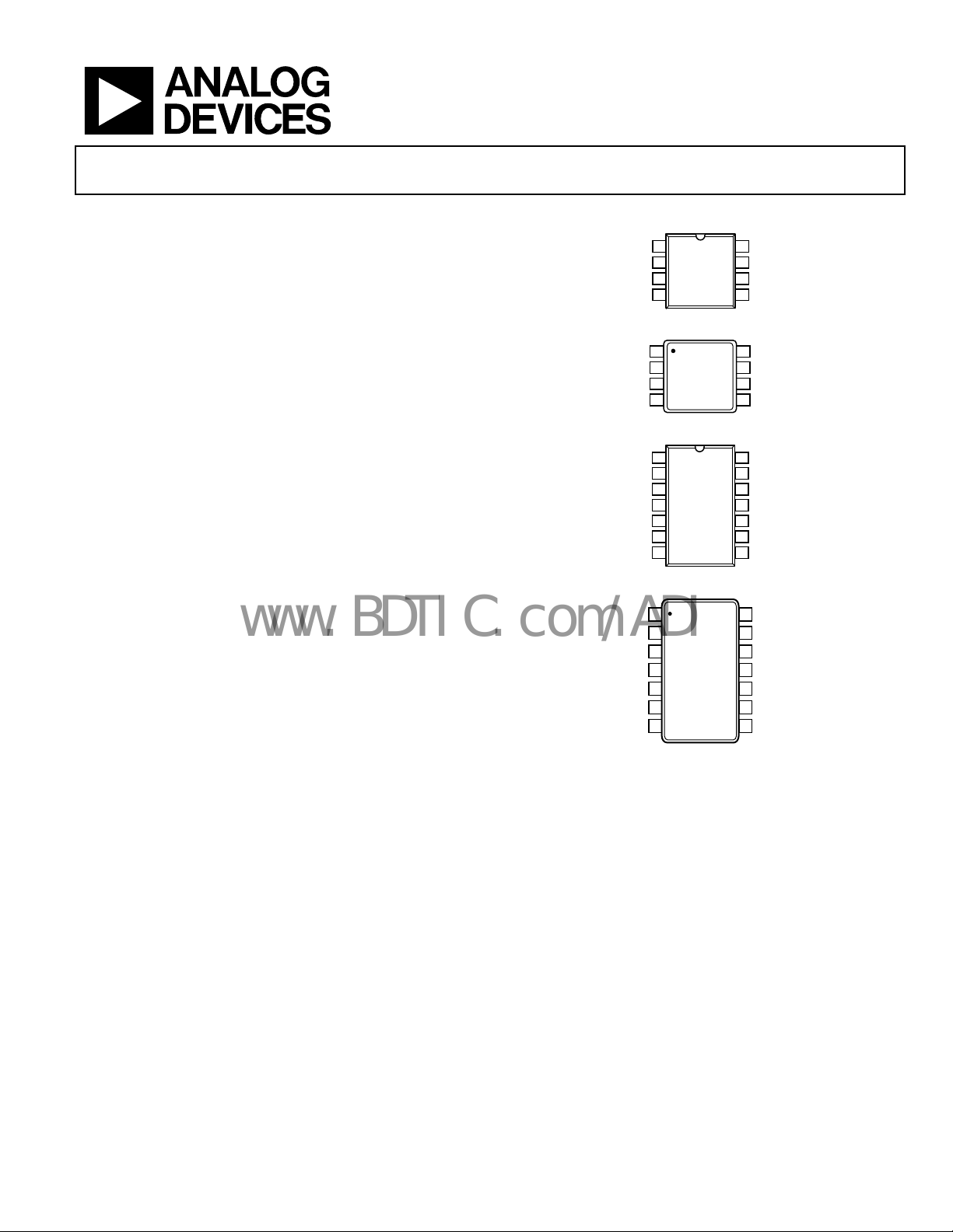
PIN CONFIGURATIONS
OUT A
1
ADTL082J
–IN A
2
TOP VIEW
3
+IN A
(Not to Scale)
4
–V
Figure 1. 8-Lead SOIC_N (R-8)
OUT A
1
ADTL082A
–IN A
2
–V
TOP VIEW
3
(Not to Scale)
4
+IN A
Figure 2. 8-Lead MSOP (RM-8)
OUT A
1
2
–IN A
+IN A
3
ADTL084J
TOP VIEW
+V
4
(Not to Scale)
5
+IN B
–IN B
6
7
OUT B
Figure 3. 14-Lead SOIC_N (R-14)
1
OUT A
2
–IN A
3
+IN A
+IN B
–IN B
UT B
+V
ADTL084A
TOP VIEW
4
(Not to Scale)
5
6
7
Figure 4. 14-Lead TSSOP (RU-14)
14
13
12
11
10
8
7
6
5
8
7
6
5
9
8
14
13
12
11
10
9
8
+V
OUT B
–IN B
+IN B
+V
OUT B
–IN B
+IN B
OUT D
–IN D
+IN D
–V
+IN C
–IN C
OUT C
OUT D
–IN D
+IN D
–V
+IN C
–IN C
OUT C
06275-001
06275-002
06275-003
06275-004
GENERAL DESCRIPTION
The ADTL082 and ADTL084 are JFET input amplifiers that
provide industry-leading performance over TL08x devices.
The ADTL082A and ADTL084A are improved versions of
TL08x A, I, and Q grades. The ADTL082J and ADTL084J are
industry alternatives to the TL08x standard and C grades.
The ADTL08x family offers lower noise, offset voltage, offset
ift over temperature, and bias current over the TL08x. In
dr
addition, the ADLT08x family has better common-mode
rejection and slew rates.
These op amps are ideal for various applications, including
p
rocess control, industrial and instrumentation equipment,
Rev. B
Information furnished by Analog Devices is believed to be accurate and reliable. However, no
responsibility is assumed by Anal og Devices for its use, nor for any infringements of patents or ot her
rights of third parties that may result from its use. Specifications subject to change without notice. No
license is granted by implication or otherwise under any patent or patent rights of Analog Devices.
Trademarks and registered trademarks are the property of their respective owners.
active filtering, data conversion, buffering, and power control
and monitoring.
The A grade amplifiers are available in lead-free packaging. The
st
andard grade amplifiers are available in both leaded and lead-
free packaging.
The ADTL082A and ADTL084A are specified over the extended
ustrial (−40°C to +125°C) temperature range. The ADTL082J
ind
and ADTL084J are specified over the commercial (0°C to 70°C)
temperature range.
One Technology Way, P.O. Box 9106, Norwood, MA 02062-9106, U.S.A.
Tel: 781.329.4700 www.analog.com
Fax: 781.461.3113 ©2007 Analog Devices, Inc. All rights reserved.
Page 2

ADTL082/ADTL084
www.BDTIC.com/ADI
TABLE OF CONTENTS
Features .............................................................................................. 1
Applications....................................................................................... 1
Pin Configurations ........................................................................... 1
General Description......................................................................... 1
Revision History ............................................................................... 2
Specifications..................................................................................... 3
Absolute Maximum Ratings............................................................ 4
REVISION HISTORY
11/07—Rev. A to Rev. B
Changes to Ordering Guide.......................................................... 10
4/07—Rev. 0 to Rev. A
Changes to Table 1............................................................................ 3
1/07—Revision 0: Initial Version
Thermal Resistance .......................................................................4
Power Sequencing .........................................................................4
ESD Caution...................................................................................4
Typical Perf or m an c e Charac t e r istics ..............................................5
Outline Dimensions ..........................................................................8
Ordering Guide .......................................................................... 10
Rev. B | Page 2 of 12
Page 3
ADTL082/ADTL084
www.BDTIC.com/ADI
SPECIFICATIONS
VCC = ±15 V, VCM = 0 V, TA = 25°C, over all grades, unless otherwise noted.
Table 1.
Parameter Symbol Conditions Min Typ Max Min Typ Max Unit
INPUT CHARACTERISTICS
Offset Voltage VOS 2 9 1.5 5.5 mV
0°C ≤ TA ≤ +70°C 10 8 mV
−40°C ≤ TA ≤ +125°C 9 mV
Offset Voltage Drift ΔVOS/ΔT 0°C ≤ TA ≤ +70°C 15 μV/°C
−40°C ≤ TA ≤ +125°C 10 μV/°C
Input Bias Current IB 2 100 2 100 pA
0°C ≤ TA ≤ +70°C 3 3 nA
−40°C ≤ TA ≤ +125°C 5 nA
Input Offset Current IOS 2 100 2 100 pA
0°C ≤ TA ≤ 70°C 3 3 nA
−40°C ≤ TA ≤ +125°C 5 nA
Input Voltage Range V
Common-Mode Rejection Ratio CMRR VCM = −11 V to +15 V 80 86 80 86 dB
Input Impedance RIN 10
Large Signal Voltage Gain A
0°C ≤ TA ≤ 70°C 90 200 90 200 V/mV
−40°C ≤ TA ≤ +125°C 50 200 V/mV
OUTPUT CHARACTERISTICS
Maximum Output Voltage Swing V
0°C ≤ TA ≤ +70°C ±12 ±13 V
−40°C ≤ TA ≤ +125°C ±13 V
R
0°C ≤ TA ≤ +70°C ±10 ±12 V
−40°C ≤ TA ≤ +125°C ±12 V
Short-Circuit Output Current ISC ±27 ±27 mA
POWER SUPPLY
Power Supply Rejection Ratio PSRR VDD = 8 V to 36 V 80 86 80 86 dB
Supply Current per Amplifier ISY 1.2 1.8 1.2 1.8 mA
0°C ≤ TA ≤ +70°C 1.9 1.9 mA
−40°C ≤ TA ≤ +125°C 2.0 mA
DYNAMIC PERFORMANCE
Slew Rate SR 20 20 V/μs
Gain Bandwidth Product GBP 5 5 MHz
Phase Margin φM 63 63 Degrees
Total Harmonic Distortion THD
Channel Separation CS f = 10 kHz 120 120 dB
NOISE PERFORMANCE
Voltage Noise Density en f = 1 kHz 16 16 nV/√Hz
CM
VO
O
−11 +15 −11 +15 V
RL = 2 kΩ,
V
= −10 V to +10 V
O
RL = 10 kΩ ±12 ±13.5 ±13 ±13.5 V
= 2 kΩ ±12.5 ±13.3 V
L
= 6 V rms, f = 1 kHz,
V
IN
= +1, RL = 2 kΩ
A
V
J Grade A Grade
12
10
100 200 100 200 V/mV
0.001 0.001 %
12
Ω
Rev. B | Page 3 of 12
Page 4
ADTL082/ADTL084
www.BDTIC.com/ADI
ABSOLUTE MAXIMUM RATINGS
Table 2.
Parameter Rating
Supply Voltage ±18 V or +36 V
Input Voltage ±V supply
Differential Input Voltage ±V supply
Output Short Circuit to GND Indefinite
Storage Temperature Range −65°C to +150°C
Operating Temperature Range −40°C to +125°C
Lead Temperature (Soldering 60 sec) 300°C
Junction Temperature 150°C
Stresses above those listed under Absolute Maximum Ratings
may cause permanent damage to the device. This is a stress
rating only; functional operation of the device at these or any
other conditions above those indicated in the operational
section of this specification is not implied. Exposure to absolute
maximum rating conditions for extended periods may affect
device reliability.
THERMAL RESISTANCE
Table 3. Thermal Resistance
Package Type θ
8-Lead SOIC_N (R-8) 158 43 °C/W
8-Lead MSOP (RM-8) 210 45 °C/W
14-Lead SOIC_N (R-14) 120 36 °C/W
14-Lead TSSOP (RU-14) 180 35 °C/W
JA
θ
Unit
JC
POWER SEQUENCING
The op amp supplies must be established simultaneously with,
or before, the application of any input signals.
If this is not possible, the input current must be limited to 10 mA.
ESD CAUTION
Rev. B | Page 4 of 12
Page 5

ADTL082/ADTL084
www.BDTIC.com/ADI
TYPICAL PERFORMANCE CHARACTERISTICS
16
VSY = ±15V
14
12
RL = 2kΩ
= 25°C
T
A
16
14
12
RL = 10kΩ
RL = 2kΩ
10
VSY = ±10V
8
6
VSY = ±5V
4
MAXIMUM PEAK O UTPUT VOL TAGE (±V)
2
OM
V
0
100
1k 10k 100k 1M 10M
FREQUENCY (Hz)
Figure 5. Maximum Peak Output Voltage vs. Frequency
16
VSY = ±15V
14
12
10
VSY = ±10V
8
6
VSY = ±5V
4
MAXIMUM PEAK OUTPUT VOLTAGE (±V)
2
OM
V
0
1k 10k 100k 1M 10M100
FREQUENCY (Hz)
Figure 6. Maximum Peak Output Voltage vs. Frequency
RL = 10kΩ
= 25°C
T
A
10
8
6
4
VSY = ±15V
MAXIMUM PEAK OUTPUT VOLTAGE (±V)
2
OM
V
0
–75 –50 –25 0 25 50 75 100 125
T
06275-005
FREE-AIR TE MPERATURE (°C)
A
06275-008
Figure 8. Maximum Peak Output Voltage vs. Free-Air Temperature
16
VSY = ±15V
14
T
= 25°C
A
12
10
8
6
4
MAXIMUM PEAK OUTPUT VOLTAGE (±V)
2
OM
V
0
06275-006
R
L
1k 10k100
LOAD RESISTANCE (Ω)
06275-009
Figure 9. Maximum Peak Output Voltage vs. Load Resistance
16
14
12
10
8
6
4
MAXIMUM PEAK O UTPUT VOL TAGE (±V)
2
OM
V
0
10k 100k 1M 10M
FREQUENCY (Hz)
TA = –55°C
TA = +125°C
VSY = ±15V
R
TA = +25°C
= 2kΩ
L
06275-007
Figure 7. Maximum Peak Output Voltage vs. Frequency
Rev. B | Page 5 of 12
16
RL = 10Ω
14
T
= 25°C
A
12
10
8
6
4
MAXIMUM PEAK OUTPUT VOLTAGE (±V)
2
OM
V
0
±4 ±5 ±6 ±7 ±8 ±9 ±10 ±11 ±12 ±13 ±14 ±15
VSY SUPPLY VOLTAGE (V)
Figure 10. Maximum Peak Output Voltage vs. Supply Voltage
06275-010
Page 6

ADTL082/ADTL084
L
www.BDTIC.com/ADI
1k
100
10
LARGE S IGNAL DIFFERENT IA
VD
A
VSY = ±15V
VOLTAGE AMPLIFI CATION (V/mV)
V
= ±10V
O
R
= 2kΩ
L
1
–75 –50 –25 0 25 50 75 100 125
FREE-AIR TEMPERATURE (°C)
T
A
Figure 11. Large Signal Differential Voltage Amplification
v
s. Free-Air Temperature
1.4
1.2
1.0
0.8
06275-011
100
VSY = ±15V
NO SIGNAL
NO LOAD
80
60
40
20
PD TOTAL POWER DISS IPATIO N (mW)
0
–75 –50 –25 0 25 50 75 100 125
T
FREE-AIR TEMPERATURE (°C)
A
Figure 14. Total Power Dissipation vs. Free-Air Temperature
4
VSY = ±15V
3
2
06275-014
0.6
SUPPLY CURRENT (mA)
0.4
SY
I
0.2
0
–75 –50 –25 0 25 50 75 100 125
FREE-AIR TE MPERATURE (°C)
T
A
VSY = ±15V
NO SIGNAL
NO LOAD
Figure 12. Supply Current Per Amplifier vs. Free-Air Temperature
2.0
TA = 25°C
1.8
NO SIGNAL
NO LOAD
1.6
1.4
1.2
1.0
0.8
0.6
SUPPLY CURRENT (mA)
SY
I
0.4
0.2
0
±4 ±5 ±6 ±7 ±8 ±9 ±10 ±11 ±12 ±13 ±14 ±15
V
SUPPLY VOLTAGE (V)
SY
Figure 13. Supply Current vs. Supply Voltage
1
INPUT BIAS CURRENT (nA)
B
I
0
–1
–55 –35 –15 5 25 45 65 85 105 125
FREE-AIR TEMPERATURE (°C)
T
06275-012
A
06275-015
Figure 15. Input Bias Current vs. Free-Air Temperature
10.0
VSY = ±15V
1.0
0.1
0.01
IB INPUT BIAS CURRENT (nA)
0.001
–55 –35 –15 5 25 45 65 85 105 125
T
FREE-AIR TE MPERATURE (°C)
06275-013
A
06275-016
Figure 16. Input Bias Current vs. Free-Air Temperature
Rev. B | Page 6 of 12
Page 7

ADTL082/ADTL084
www.BDTIC.com/ADI
6
4
2
0
–2
INPUT AND OUTPUT VOLT AGE (V)
–4
–6
–2 0 2 4 6 8 10
OUTPUT
INPUT
TIME (µs)
VSY = ±15V
R
= 2kΩ
L
C
= 100pF
L
T
= 25°C
A
Figure 17. Large Signal Response
06275-017
90
80
70
60
50
40
(nV/√Hz)
30
20
EQUIVALENT INPUT NOISE VOLT AGE
N
10
V
0
10 100 1k 10k1
FREQUENCY (Hz)
VSY = ±15V
A
= 1k
V
T
= 25°C
A
06275-020
Figure 20. Voltage Noise Density vs. Frequency
0.15
0.10
0.05
0
VSY = ±15V
R
= 2kΩ
–0.05
OUTPUT VO LTAGE (V )
O
V
–0.10
–0.15
–0.2 0 0.2 0.4 0.6 0.8 1.0 1.2
ELAPSED TIME (µs)
L
C
= 100pF
L
T
= 25°C
A
Figure 18. Small Signal Response
95
VSY = ±15V
94
93
92
1
VSY = ±15V
A
= 1
V
Vi (rms) = 6V
T
= 25°C
A
0.1
0.01
0.001
THD TOTAL HARMONIC DISTORTIO N (%)
0.0001
06275-018
100 1000 10000 10000010
FREQUENCY (Hz)
06275-021
Figure 21. Total Harmonic Distortion vs. Frequency
91
90
CMRR COMMON MO DE REJECTIO N RATIO (d B)
89
–55 –35 –15 5 25 45 65 85 105 125
FREE-AIR TEMPERATURE (° C)
T
A
06275-019
Figure 19. Common-Mode Rejection Ratio vs. Free-Air Temperature
Rev. B | Page 7 of 12
Page 8

ADTL082/ADTL084
www.BDTIC.com/ADI
OUTLINE DIMENSIONS
5.00 (0.1968)
4.80 (0.1890)
4.00 (0.1574)
3.80 (0.1497)
0.25 (0.0098)
0.10 (0.0040)
COPLANARITY
0.10
CONTROLL ING DIMENSI ONS ARE IN MILLIMETERS; INCH DI MENSIONS
(IN PARENTHESES) ARE ROUNDED-OFF MILLIMETER EQUIVALENTS FOR
REFERENCE ONLY AND ARE NOT APPROPRI ATE FOR USE IN DES IGN.
85
1
1.27 (0.0500)
SEATING
PLANE
COMPLIANT TO JEDEC STANDARDS MS-012-A A
BSC
6.20 (0.2441)
5.80 (0.2284)
4
1.75 (0.0688)
1.35 (0.0532)
0.51 (0.0201)
0.31 (0.0122)
8°
0°
0.25 (0.0098)
0.17 (0.0067)
Figure 22. 8-Lead Standard Small Outline Package [SOIC_N]
Narrow B
ody (R-8)
Dimensions shown in millimeters and (inches)
3.20
3.00
2.80
8
5
3.20
3.00
2.80
1
5.15
4.90
4.65
4
0.50 (0.0196)
0.25 (0.0099)
1.27 (0.0500)
0.40 (0.0157)
45°
012407-A
PIN 1
0.65 BSC
0.95
0.85
0.75
0.15
0.38
0.00
0.22
COPLANARITY
0.10
COMPLIANT TO JEDEC STANDARDS MO-187-AA
1.10 MAX
SEATING
PLANE
0.23
0.08
8°
0°
Figure 23. 8-Lead Mini Small Outline Package [MSOP]
(RM-8)
Dim
ensions shown in millimeters
0.80
0.60
0.40
Rev. B | Page 8 of 12
Page 9

ADTL082/ADTL084
www.BDTIC.com/ADI
4.00 (0.1575)
3.80 (0.1496)
0.25 (0.0098)
0.10 (0.0039)
COPLANARIT Y
0.10
CONTROLL ING DIMENSIONS ARE IN MILLI METERS; INCH DIMENSIONS
(IN PARENTHESES) ARE ROUNDED-O FF MIL LIMETE R EQUIVALENTS FOR
REFERENCE ON LY AND ARE NOT APPROPRI ATE FOR USE IN DESIGN.
8.75 (0.3445)
8.55 (0.3366)
BSC
8
7
6.20 (0.2441)
5.80 (0.2283)
1.75 (0.0689)
1.35 (0.0531)
SEATING
PLANE
0.25 (0.0098)
0.17 (0.0067)
14
1
1.27 (0.0500)
0.51 (0.0201)
0.31 (0.0122)
COMPLIANT TO JEDEC STANDARDS MS-012-AB
0.50 (0.0197)
0.25 (0.0098)
8°
0°
1.27 (0.0500)
0.40 (0.0157)
45°
060606-A
Figure 24. 14-Lead Standard Small Outline Package [SOIC_N]
Narrow B
ody (R-14)
Dimensions shown in millimeters and (inches)
5.10
5.00
4.90
14
4.50
4.40
4.30
PIN 1
1.05
1.00
0.80
0.65
BSC
0.15
0.05
COMPLIANT TO JEDEC STANDARDS MO-153-AB-1
Figure 25. 14-Lead Thin Shrink S
8
6.40
BSC
71
0.20
1.20
0.09
MAX
0.30
SEATING
0.19
PLANE
COPLANARITY
0.10
mall Outline Package [TSSOP]
(RU-14)
Dimensions shown in millimeters
8°
0°
0.75
0.60
0.45
Rev. B | Page 9 of 12
Page 10

ADTL082/ADTL084
www.BDTIC.com/ADI
ORDERING GUIDE
Model Temperature Range Package Description Package Option Branding
ADTL082JR 0°C to +70°C 8-Lead SOIC_N R-8
ADTL082JR-REEL 0°C to +70°C 8-Lead SOIC_N R-8
ADTL082JR-REEL7 0°C to +70°C 8-Lead SOIC_N R-8
ADTL082JRZ
ADTL082JRZ-REEL
ADTL082JRZ-REEL7
ADTL082ARZ
ADTL082ARZ-REEL
ADTL082ARZ-REEL7
ADTL082ARMZ-R2
ADTL082ARMZ-REEL
ADTL084JR 0°C to +70°C 14-Lead SOIC_N R-14
ADTL084JR-REEL 0°C to +70°C 14-Lead SOIC_N R-14
ADTL084JR-REEL7 0°C to +70°C 14-Lead SOIC_N R-14
ADTL084JRZ
ADTL084JRZ-REEL
ADTL084JRZ-REEL7
ADTL084ARZ
ADTL084ARZ-REEL
ADTL084ARZ-REEL7
ADTL084ARUZ
ADTL084ARUZ-REEL
1
Z = RoHS Compliant Part.
1
1
1
1
1
1
1
1
1
1
1
1
1
1
1
1
0°C to +70°C 8-Lead SOIC_N R-8
0°C to +70°C 8-Lead SOIC_N R-8
0°C to +70°C 8-Lead SOIC_N R-8
−40°C to +125°C 8-Lead SOIC_N R-8
−40°C to +125°C 8-Lead SOIC_N R-8
−40°C to +125°C 8-Lead SOIC_N R-8
−40°C to +125°C 8-Lead MSOP RM-8 A18
−40°C to +125°C 8-Lead MSOP RM-8 A18
0°C to +70°C 14-Lead SOIC_N R-14
0°C to +70°C 14-Lead SOIC_N R-14
0°C to +70°C 14-Lead SOIC_N R-14
−40°C to +125°C 14-Lead SOIC_N R-14
−40°C to +125°C 14-Lead SOIC_N R-14
−40°C to +125°C 14-Lead SOIC_N R-14
−40°C to +125°C 14-lead TSSOP RU-14
−40°C to +125°C 14-lead TSSOP RU-14
Rev. B | Page 10 of 12
Page 11

ADTL082/ADTL084
www.BDTIC.com/ADI
NOTES
Rev. B | Page 11 of 12
Page 12

ADTL082/ADTL084
www.BDTIC.com/ADI
NOTES
©2007 Analog Devices, Inc. All rights reserved. Trademarks and
registered trademarks are the property of their respective owners.
D06275-0-11/07(B)
Rev. B | Page 12 of 12
 Loading...