

Page 1
±1°C Accurate, 12-Bit Digital
T
www.BDTIC.com/ADI
FEATURES
12-bit temperature-to-digital converter
B grade accuracy ±1.0°C from 0°C to 70°C
A grade accuracy ±2.0°C from –25°C to +100°C
SMBus/I
Operation from −55°C to +125°C
Operation from 3 V to 5.5 V
Overtemperature indicator
Shutdown mode for low power consumption
Power consumption 79 μW typically at 3.3 V
Small, low cost 8-pin MSOP in Pb-Sn and Pb-free packages
Standard 8-pin SOIC Pb-free package
APPLICATIONS
Isolated sensors
Environmental control systems
Computer thermal monitoring
Thermal protection
Industrial process control
Power-system monitors
Hand-held applications
2
C-compatible interface
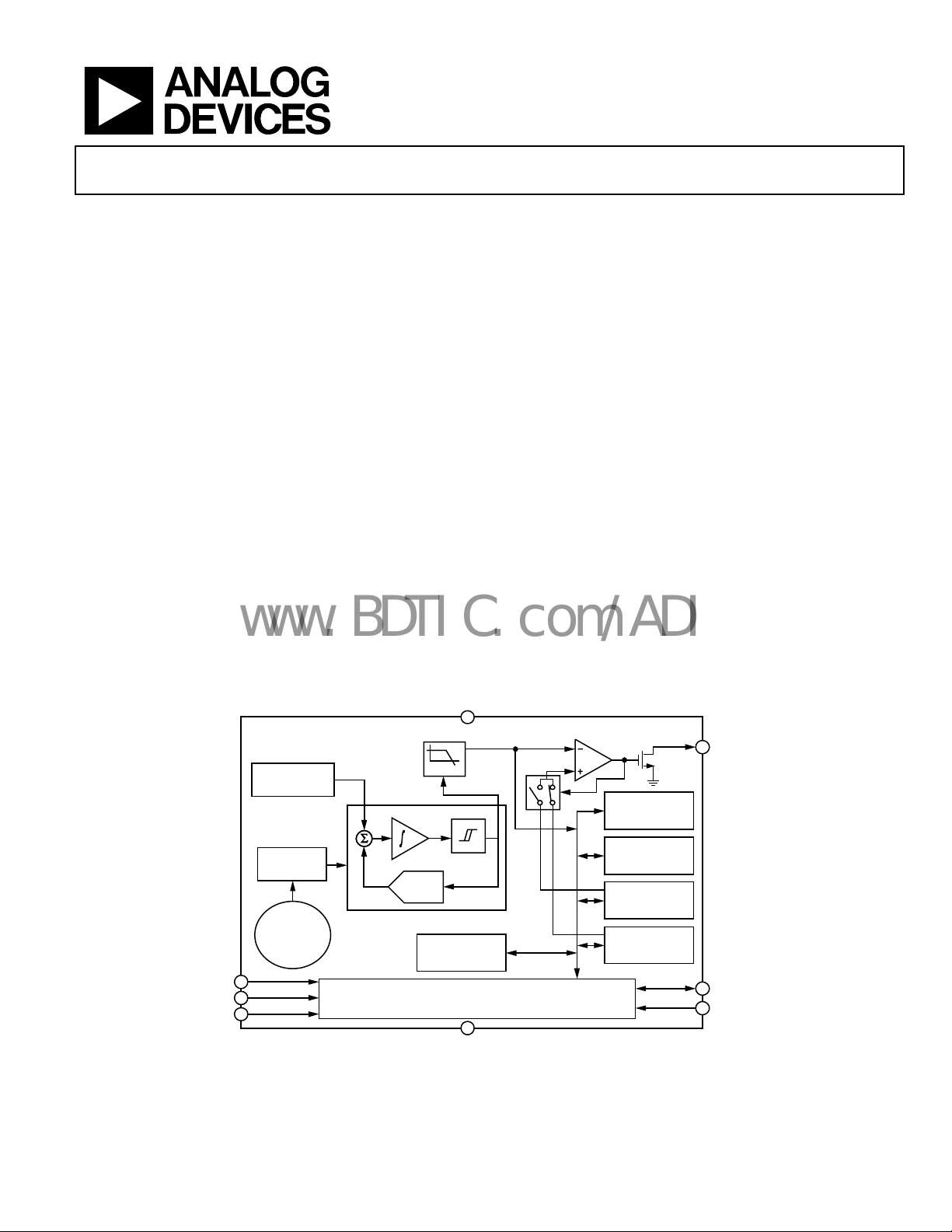
TEMPERATURE
GENERATION
7
A0
6
A1
5
A2
SENSOR
REFERENCE
CLK AND
TIMING
FUNCTIONAL BLOCK DIAGRAM
DECIMATOR
+
–
Σ-Δ
1-BIT
DAC
SMBus/I
V
DD
8
LPF
1-BIT
POINTER
REGISTER
2
C INTERFACE
8
GND
Figure 1.
Temperature Sensor
PRODUCT HIGHLIGHTS
1. On-chip temperature sensor allows an accurate
measurement of the ambient temperature. The measurable
temperature range is −55°C to +125°C.
2. S
upply voltage is 3.0 V to 5.5 V.
3. S
pace-saving, 8-lead MSOP and 8-lead SOIC.
4. T
emperature accuracy is ±1°C maximum.
5. T
emperature resolution is 0.0625°C.
6. Sh
utdown mode reduces the current consumption to
3 A typical.
onnect up to eight ADT75s to a single SMBus/I
7. C
DIGITAL
12-BIT
COMPARATOR
TEMPERATURE
SENSOR
REGISTER
CONFIGURATION
REGISTER
T
SETPOINT
HYST
REGISTER
TOS SETPOINT
REGISTER
3
OS/ALER
1
SDA
2
SCL
05326-001
ADT75
2
C bus.
Rev. 0
Information furnished by Analog Devices is believed to be accurate and reliable. However, no
responsibility is assumed by Anal og Devices for its use, nor for any infringements of patents or ot her
rights of third parties that may result from its use. Specifications subject to change without notice. No
license is granted by implication or otherwise under any patent or patent rights of Analog Devices.
Trademarks and registered trademarks are the property of their respective owners.
One Technology Way, P.O. Box 9106, Norwood, MA 02062-9106, U.S.A.
Tel: 781.329.4700 www.analog.com
Fax: 781.461.3113 © 2005 Analog Devices, Inc. All rights reserved.
Page 2

ADT75
www.BDTIC.com/ADI
TABLE OF CONTENTS
Features.............................................................................................. 1
Temperature Data Format......................................................... 11
Applications....................................................................................... 1
Product Highlights ........................................................................... 1
Functional Block Diagram .............................................................. 1
General Description ......................................................................... 3
Specifications..................................................................................... 4
A Grade.......................................................................................... 4
B Grade .......................................................................................... 5
Timing Specifications and Diagram .......................................... 6
Absolute Maximum Ratings............................................................ 7
ESD Caution.................................................................................. 7
Pin Configuration and Function Descriptions............................. 8
Typical Performance Characteristics ............................................. 9
Theory of Operation ...................................................................... 10
Circuit Information.................................................................... 10
Converter Details........................................................................ 10
One-Shot Mode .......................................................................... 12
Fault Queue................................................................................. 12
Registers....................................................................................... 13
Serial Interface............................................................................ 16
Writing data ................................................................................ 17
Reading Data............................................................................... 18
OS/ALERT Output Overtemperature Modes ........................ 19
SMBus Alert................................................................................ 20
Application Information................................................................ 21
Thermal Response Time ........................................................... 21
Self-Heating Effects.................................................................... 21
Supply Decoupling..................................................................... 21
Temperature Monitoring........................................................... 22
Outline Dimensions....................................................................... 23
Ordering Guide .......................................................................... 23
Functional Description.............................................................. 10
REVISION HISTORY
10/05—Revision O: Initial Version
Rev. 0 | Page 2 of 24
Page 3

ADT75
www.BDTIC.com/ADI
GENERAL DESCRIPTION
The ADT75 is a complete temperature monitoring system in 8-lead
MSOP and SOIC packages. It contains a bandgap temperature sensor and 12-bit ADC to monitor and digitize the temperature to a
resolution of 0.0625°C. The ADT75 is pin and register compatible
with the LM75 and AD7416.
The ADT75 is guaranteed to operate at supply voltages from 3 V
o 5.5 V. Operating at 3.3 V, the average supply current is typically
t
200 A.
The ADT75 offers a shutdown mode that powers down the
de
vice and gives a shutdown current of typically 3 A. The
ADT75 is rated for operation over the –55°C to +125°C
temperature range.
Pin A0, Pin A1, and Pin A2 are available for address selection. The
OS/ALER
temperature exceeds a programmable limit. The OS/ALERT pin
can operate in either comparator or interrupt mode.
T pin is an open-drain output that becomes active when
Rev. 0 | Page 3 of 24
Page 4

ADT75
www.BDTIC.com/ADI
SPECIFICATIONS
A GRADE
TA = T
Table 1.
Parameter Min Typ Max Unit Test Conditions/Comments
TEMPERATURE SENSOR AND ADC
OS/ALERT OUTPUT (OPEN DRAIN)
DIGITAL INPUTS
DIGITAL OUTPUT (OPEN DRAIN)
POWER REQUIREMENTS
to T
MIN
Accuracy at VDD = 3.0 V to 5.5 V ±2 °C TA = −25°C to +100°C
±3 °C TA = −55°C to +100°C
Accuracy at VDD = 3.0 V to 3.6 V ±3 °C TA = +100°C to +125°C
Accuracy at VDD = 4.5 V to 5.5 V ±2 °C TA = +100°C to +125°C
ADC Resolution 12 Bits
Temperature Resolution 0.0625 °C
Temperature Conversion Time 60 ms
Update Rate 100 ms Conversion started every 100 ms
Long Term Drift 0.08 °C Drift over 10 years, if part is operated at 55°C
Temperature Hysteresis +0.03 °C Temperature cycle = 25°C to 125°C to 25°C
Output Low Voltage, VOL 0.4 V IOL = 3 mA
Pin Capacitance 10 pF
High Output Leakage Current, IOH 0.1 5 μA OS/ALERT pin pulled up to 5.5 V
RON Resistance (Low Output) 15 Ω Supply and temperature dependent
Input Current ±1 μA VIN = 0 V to VDD
Input Low Voltage, VIL 0.3 × VDD V
Input High Voltage, VIH 0.7 × VDD V
SCL, SDA Glitch Rejection 50 ns
Pin Capacitance 3 10 pF
Output High Current, I
Output Low Voltage, VOL 0.4 V IOL = 3 mA
Output High Voltage, VOH 0.7 × VDD V
Output Capacitance, C
Supply Voltage 3 5.5 V
Supply Current at 3.3 V 350 500 μA
Supply Current at 5.0 V 380 525 μA
Average Current at 3.3 V 200 μA Part converting and I2C interface inactive
Average Current at 5.0 V 225 μA Part converting and I2C interface inactive
Shutdown Mode at 3.3 V 3 8 μA Supply current in shutdown mode
Shutdown Mode at 5.0 V 5.5 12 μA Supply current in shutdown mode
Average Power Dissipation 798.6 μW VDD = 3.3 V, normal mode at 25°C
1 SPS 78.6 μW
140 μW
, VDD = 3.0 V to 5.5 V. All specifications for −55°C to +125°C, unless otherwise noted.
MAX
Input filtering suppresses n
than 50 ns
OH
OUT
1 mA VOH = 5 V
3 10 pF
Peak current while converting and I
inactive
Peak current while converting and I
inactive
Average power dissipated for V
mode at 25°C
Average power dissipated for V
mode at 25°C
oise spikes of less
2
C interface
2
C interface
= 3.3 V, shutdown
DD
= 5.0 V, shutdown
DD
Rev. 0 | Page 4 of 24
Page 5

ADT75
www.BDTIC.com/ADI
B GRADE
TA = T
Table 2.
Parameter Min Typ Max Unit Test Conditions/Comments
TEMPERATURE SENSOR AND ADC
OS/ALERT OUTPUT (OPEN DRAIN)
DIGITAL INPUTS
DIGITAL OUTPUT (OPEN DRAIN)
POWER REQUIREMENTS
to T
MIN
Accuracy at VDD = 3.0 V to 5.5 V ±1 °C TA = 0°C to +70°C
±2 °C TA = −25°C to +100°C
±3 °C TA = −55°C to +100°C
Accuracy at VDD = 3.0 V to 3.6 V ±3 °C TA = +100°C to +125°C
Accuracy at VDD = 4.5 V to 5.5 V ±2 °C TA = +100°C to +125°C
ADC Resolution 12 bits
Temperature Resolution 0.0625 °C
Temperature Conversion Time 60 ms
Update Rate 100 ms Conversion started every 100 ms
Long Term Drift 0.08 °C Drift over 10 years, if part is operated at 55°C
Temperature Hysteresis +0.03 °C Temperature cycle = 25°C to 125°C to 25°C
Output Low Voltage, VOL 0.4 V IOL = 3 mA
Pin Capacitance 10 pF
High Output Leakage Current, IOH 0.1 5 μA OS/ALERT pin pulled up to 5.5 V
RON Resistance (Low Output) 15 Ω Supply and temperature dependent
Input Current ±1 μA VIN = 0 V to VDD
Input Low Voltage, VIL 0.3 × VDD V
Input High Voltage, VIH 0.7 × VDD V
SCL, SDA Glitch Rejection 50 ns
Pin Capacitance 3 10 pF
Output High Current, I
Output Low Voltage, VOL 0.4 V IOL = 3 mA
Output High Voltage, VOH 0.7 × VDD V
Output Capacitance, C
Supply Voltage 3 5.5 V
Supply Current at 3.3 V 350 500 μA
Supply Current at 5.0 V 380 525 μA
Average Current at 3.3 V 200 μA Part converting and I2C interface inactive
Average Current at 5.0 V 225 μA Part converting and I2C interface inactive
Shutdown Mode at 3.3 V 3 8 μA Supply current in shutdown mode
Shutdown Mode at 5.0 V 5.5 12 μA Supply current in shutdown mode
Average Power Dissipation 798.6 μW VDD = 3.3 V, normal mode at 25°C
1 SPS 78.6 μW
140 μW
, VDD = 3.0 V to 5.5 V. All specifications for −55°C to +125°C, unless otherwise noted.
MAX
Input filtering suppresses n
than 50 ns
OH
OUT
1 mA VOH = 5 V
3 10 pF
Peak current while converting and I
interface inactive
Peak current while converting and I
interface inactive
Average power dissipated for V
mode at 25°C
Average power dissipated for V
mode at 25°C
oise spikes of less
2
C
2
C
= 3.3 V, shutdown
DD
= 5.0 V, shutdown
DD
Rev. 0 | Page 5 of 24
Page 6

ADT75
T
www.BDTIC.com/ADI
TIMING SPECIFICATIONS AND DIAGRAM
Measure the SDA and SCL timing with the input filters turned on to meet the fast mode I2C specification. Switching off the input filters
improves the transfer rate but has a negative affect on the EMC behavior of the part.
T
= T
MIN
to T
A
Table 3.
Parameter
Serial Clock Period, t1 2.5 μs Fast mode I2C. See Figure 2
Data In Setup Time to SCL High, t2 50 ns See Figure 2
Data Out Stable After SCL Low, t3 0 0.9
Data Out Stable After SCL Low, t3 0 3.45
SDA Low Setup Time to SCL Low (Start Condition), t4 50 ns See Figure 2
SDA High Hold Time After SCL High (Stop Condition), t5 50 ns See Figure 2
SDA and SCL Rise Time, t6 300 ns Fast mode I2C. See Figure 2
SDA and SCL Rise Time, t6 1000 ns Standard mode I2C. See Figure 2
SDA and SCL Fall Time, t7 300 ns See Figure 2
Capacitive Load for each Bus Line, C
1
Guaranteed by design and characterization; not production tested.
2
This time has to be met only if the master does not stretch the low period of the SCL signal.
, VDD = +2.7 V to +5.5 V, unless otherwise noted.
MAX
1
B
SCL
t
SDA
DATA IN
SDA
DATA OU
MIN TYP MAX Units Comments
2
ns Fast mode I2C. See Figure 2
2
μs Standard mode I2C. See Figure 2
400 pF
t
1
t
4
2
Figure 2. SMBus/I
t
3
2
C Timing Diagram
t
5
t
t
7
6
05326-002
Rev. 0 | Page 6 of 24
Page 7
ADT75
www.BDTIC.com/ADI
ABSOLUTE MAXIMUM RATINGS
Table 4.
Parameter Rating
VDD to GND –0.3 V to +7 V
SDA Input Voltage to GND –0.3 V to VDD + 0.3 V
SDA Output Voltage to GND –0.3 V to VDD + 0.3 V
SCL Input Voltage to GND –0.3 V to VDD + 0.3 V
OS/ALERT Output Voltage to GND –0.3 V to VDD + 0.3 V
Operating Temperature Range –55°C to +150°C
Storage Temperature Range –65°C to +160°C
Maximum Junction Temperature, T
150.7°C
JMAX
8-Lead MSOP (RM-8)
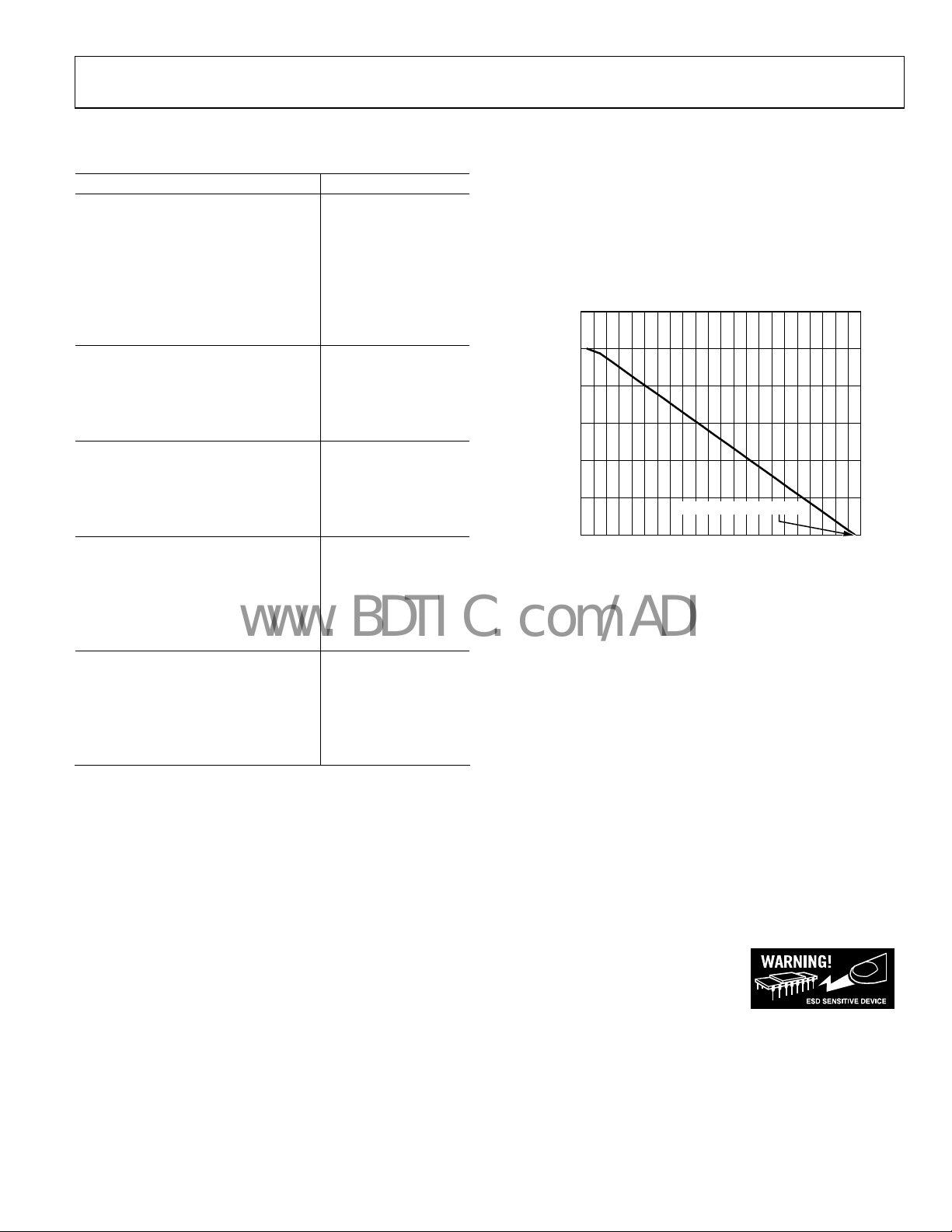
Power Dissipation1,
Thermal Impedance
2
3
W
= (T
MAX
− TA)/θJA
JMAX
θJA, Junction-to-Ambient (Still Air) 205.9°C/W
θJC, Junction-to-Case 43.74°C/W
8-Lead SOIC (R-8)
Power Dissipation1, 2 W
MAX
= (T
− TA)/θJA
JMAX
Thermal Impedance3
θJA, Junction-to-Ambient (Still Air) 157°C/W
θJC, Junction-to-Case 56°C/W
IR Reflow Soldering
Peak Temperature 220°C (0°C/5°C)
Time at Peak Temperature 10 sec to 20 sec
Ramp-Up Rate 3°C/sec maximum
Ramp-Down Rate –6°C/sec maximum
Time 25°C to Peak Temperature 6 minutes maximum
IR Reflow Soldering (Pb-Free Package)
Peak Temperature 260°C (+0°C)
Time at Peak Temperature 20 sec to 40 sec
Ramp-Up Rate 3°C/sec maximum
Ramp-Down Rate –6°C/sec maximum
Time 25°C to Peak Temperature 8 minutes maximum
1
Values relate to package being used on a standard 2-layer PCB. This gives a
worst case θ
dissipation vs. ambient temperature (T
2
TA = ambient temperature.
3
Junction-to-case resistance is applicable to components featuring a
preferential flow direction, for example, components mounted on a heat
sink. Junction-to-ambient resistance is more useful for air-cooled, PCBmounted components.
and θJC. Refer to Figure 3 for a plot of maximum power
JA
).
A
Stresses above those listed under Absolute Maximum Ratings
may cause permanent damage to the device. This is a stress
rating only; functional operation of the device at these or any
other conditions above those indicated in the operational
section of this specification is not implied. Exposure to absolute
maximum rating conditions for extended periods may affect
device reliability.
1.2
1.0
0.8
0.6
0.4
0.2
MAXIMUM POWER DISSIPATION (Watts)
0
–55
–50
–40
–30
Figure 3. MSOP Maximum Power Dissipation vs. Ambient Temperature
MAX PD = 3.4mW AT 150°C
0
102030405060708090
–20
–10
TEMPERATURE (°C)
100
110
120
130
140
150
05326-003
ESD CAUTION
ESD (electrostatic discharge) sensitive device. Electrostatic charges as high as 4000 V readily accumulate on
the human body and test equipment and can discharge without detection. Although this product features
proprietary ESD protection circuitry, permanent damage may occur on devices subjected to high energy
electrostatic discharges. Therefore, proper ESD precautions are recommended to avoid performance degradation or loss of functionality.
Rev. 0 | Page 7 of 24
Page 8

ADT75
T
www.BDTIC.com/ADI
PIN CONFIGURATION AND FUNCTION DESCRIPTIONS
SDA
Table 5. Pin Function Descriptions
Pin No. Mnemonic Description
1 SDA
SMBus/I
2
C Serial Data Input/Output. Serial data that is loaded into and read from the ADT75 registers is provided
on this pin. Open-drain configuration; needs a pull-up resistor.
2 SCL
Serial Clock Input. This is the clock input for the serial port. The serial clock is used to clock in and clock out data to
and from any register of the ADT75. Open-drain configuration; needs a pull-up resistor.
3 OS/ALERT
Over- and Undertemperature Indicator. Default power as an OS pin. Open-drain configuration; needs a pull-
up resistor.
4 GND
5 A2
6 A1
7 A0
8 V
Positive Supply Voltage, 3 V to 5.5 V. The supply should be decoupled to ground.
DD
Analog and Digital Ground.
SMBus/I2C Serial Bus Address Selection Pin. Logic input. Can be set to GND or VDD.
SMBus/I2C Serial Bus Address Selection Pin. Logic input. Can be set to GND or VDD.
SMBus/I2C Serial Bus Address Selection Pin. Logic input. Can be set to GND or VDD.
1
SCL
OS/ALER
GND
Figure 4. Pin Configuration
ADT75
2
TOP VIEW
3
(Not to Scale)
4
V
8
DD
A0
7
6
A1
A2
5
05326-004
Rev. 0 | Page 8 of 24
Page 9

ADT75
www.BDTIC.com/ADI
TYPICAL PERFORMANCE CHARACTERISTICS
1.0
0.8
0.6
0.4
0.2
0
–0.2
–0.4
TEMPERATURE ERROR (°C)
–0.6
–0.8
–1.0
–55 125
–35 –15 5 25 45 65 85 105
VDD = 3.3V
VDD = 5V
TEMPERATURE (°C)
05326-023
7
= 30°C
T
A
6
5
4
3
2
SHUTDOWN CURRENT (μA)
1
0
3.0
3.5 4.0 4.5 5.0
SUPPLY VOLTAGE (V)
5.5
05326-026
Figure 5. Temperature Accuracy at 3.3 V and 5 V
500
CONVERTING @ 5.5V
450
400
350
300
250
200
150
SUPPLY CURRENT (μA)
100
50
0
–55 125
CONVERTING @ 3.3V
AVERAGE @ 5.5V
AVERAGE @ 3.3V
–35 –15 5 25 45 65 85 105
TEMPERATURE (°C)
Figure 6. Operating Supply Current vs. Temperature
260
T
= 30°C
A
240
220
200
180
160
140
AVERAGE SUPPLY CURRENT (μA)
120
100
3.0
3.5 4.0 4.5 5.0
SUPPLY VOLTAGE (V)
5.5
05326-024
05326-025
Figure 8. Shutdown Current vs. Supply Voltage at 30°C
0.05
TA = 25°C
A 0.1μF CAPACITOR IS CONNECTED AT THE V
0.04
0.03
0.02
0.01
0
–0.01
–0.02
TEMPERATURE ERROR (°C)
–0.03
–0.04
–0.05
0
VDD = 3.3V ± 10%
0.5 1.0 1.5 2.0 2.5 3.0 3.5 4.0 4.5
SUPPLY RIPPLE FREQUENCY (MHz)
VDD = 5V ± 10%
PIN.
DD
05326-027
5.0
Figure 9. Temperature Accuracy vs. Supply Ripple Frequency
0.025
0.020
0.015
0.010
0.005
0
–0.005
SOIC PACKAGE
–0.010
TEMPERATURE ERROR (°C)
–0.015
–0.020
–0.025
01
MSOP PACKAGE
24681012
RECOVERY TIME AT 25°C (Hours)
05326-028
4
Figure 7. Average Operating Supply Curre
nt vs. Supply Voltage at 30°C
Rev. 0 | Page 9 of 24
Figure 10. Response to Thermal Shock
Page 10

ADT75
www.BDTIC.com/ADI
THEORY OF OPERATION
CIRCUIT INFORMATION
The ADT75 is a 12-bit digital temperature sensor with the 12th bit
acting as the sign bit. An on-board temperature sensor generates a
voltage precisely proportional to absolute temperature that is
compared to an internal voltage reference and input to a precision
digital modulator. Overall accuracy for the ADT75 A Grade is
±2°C from −25°C to +100°C and accuracy for the ADT75 B Grade
is ±1°C from 0°C to +70°C. Both grades have excellent transducer
linearity. The serial interface is SMBus /I
2
C- compatible and the
open-drain output of the ADT75 is capable of sinking 3 mA.
The on-board temperature sensor has excellent accuracy and
arity over the entire rated temperature range without
line
needing correction or calibration by the user.
The sensor output is digitized by a first-order ∑-∆ modulator,
own as the charge balance type analog-to-digital
also kn
converter. This type of converter utilizes time-domain oversampling and a high accuracy comparator to deliver 12 bits of
effective accuracy in an extremely compact circuit.
CONVERTER DETAILS
The ∑-∆ modulator consists of an input sampler, a summing
network, an integrator, a comparator, and a 1-bit DAC. Similar
to the voltage-to-frequency converter, this architecture creates a
negative feedback loop and minimizes the integrator output by
changing the duty cycle of the comparator output in response to
input voltage changes. The comparator samples the output of
the integrator at a much higher rate than the input sampling
frequency; this is called oversampling. Oversampling spreads
the quantization noise over a much wider band than that of the
input signal, improving overall noise performance and
increasing accuracy.
Σ-Δ MODULATOR
INTEGRATOR
VOLTAGE REF
AND VPTAT
CLOCK
GENERATOR
+
–
Figure 11. First-Order ∑-
The modulated output of the comparator is encoded using a
circuit technique that results in SMBus/I
1-BIT
DAC
LPF DIGITAL
FILTER
COMPARATOR
1-BIT
12-BIT
Δ Modulator
2
C temperature data.
TEMPERATURE
VALUE
REGISTER
05326-011
FUNCTIONAL DESCRIPTION
The conversion clock for the part is generated internally. No
external clock is required except when reading from and
writing to the serial port. In normal mode, the internal clock
oscillator runs an automatic conversion sequence. During this
automatic conversion sequence, a conversion is initiated every
100 ms. At this time, the part powers up its analog circuitry and
performs a temperature conversion.
This temperature conversion typically takes 60 ms, after which
me the analog circuitry of the part automatically shuts down.
ti
The analog circuitry powers up again 40 ms later, when the 100 ms
timer times out and the next conversion begins. The result of the
most recent temperature conversion is always available in the
temperature value register because the SMBus/I
shuts down.
The ADT75 can be placed in sh
utdown mode via the
configuration register, in which case the on-chip oscillator is
shut down and no further conversions are initiated until the
ADT75 is taken out of shutdown mode. The ADT75 can be
taken out of shutdown mode by writing 0 to Bit D0 in the
configuration register. The ADT75 typically takes 1.7 ms to
come out of shutdown mode. The conversion result from the
last conversion prior to shutdown can still be read from the
ADT75 even when it is in shutdown mode.
In normal conversion mode, the internal clock oscillator is reset
fter every read or write operation. This causes the device to
a
start a temperature conversion, the result of which is typically
available 60 ms later. Similarly, when the part is taken out of
shutdown mode, the internal clock oscillator is started and a
conversion is initiated.
The conversion result is typically available 60 ms later. Reading
f
rom the device before a conversion is complete causes the
ADT75 to stop converting; the part starts again when serial
communication is finished. This read operation provides the
previous conversion result.
The measured temperature value is compared with a high
emperature limit, stored in the 16-bit T
t
and the hysteresis temperature limit, stored in the 16-bit
T
read/write register. If the measured value exceeds these
HYST
limits then the OS/ALERT pin is activated. This OS/ALERT
pin is programmable for mode and polarity via the configuration register.
2
C circuitry never
read/write register
OS
Rev. 0 | Page 10 of 24
Page 11

ADT75
www.BDTIC.com/ADI
Configuration register functions consist of
witching between normal operation and full power-down.
• S
• S
witching between comparator and interrupt event modes.
etting the OS/ALERT pin active polarity.
• S
• S
etting the number of faults that activate the
OS/ALERT pin.
• Ena
• Ena
bling the one-shot mode.
bling the SMBus alert function mode on the
OS/ALERT pin.
TEMPERATURE DATA FORMAT
One LSB of the ADC corresponds to 0.0625°C. The ADC can
theoretically measure a temperature range of 255°C (−128°C to
+127°C ), but the ADT75 is guaranteed to measure a low value
temperature limit of −55°C to a high value temperature limit of
+125°C. The temperature measurement result is stored in the
16-bit temperature value register and is compared with the high
temperature limit stored in the T
hysteresis limit in the T
HYST
Temperature data in the temperature value register, the T
setpoint register and the T
HYST
by a 12-bit twos complement word. The MSB is the temperature
sign bit. The four LSBs, Bit DB0 to Bit DB3, are not part of the
temperature conversion result and are always 0s.
t
he temperature data format without Bit DB0 to Bit DB3.
setpoint register and the
OS
setpoint register.
setpoint register, is represented
Tabl e 6 shows
OS
Table 6. 12-Bit Temperature Data Format
Temperature
Digital Output (Binary)
DB15 to DB4
Digital Output (Hex)
−55°C 1100 1001 0000 0xC90
−50°C 1100 1110 0000 0xCE0
−25°C 1110 0111 0000 0xE70
−0.0625°C 1111 1111 1111 0xFFF
0°C 0000 0000 0000 0x000
+0.0625°C 0000 0000 0001 0x001
+10°C 0000 1010 0000 0x0A0
+25°C 0001 1001 0000 0x190
+50°C 0011 0010 0000 0x320
+75°C 0100 1011 0000 0x4B0
+100°C 0110 0100 0000 0x640
+125°C 0111 1101 0000 0x7D0
Temperature Conversion Formulas
12-Bit Temperature Data Format
• P
ositive Temperature = ADC Code(d)/16
1
egative Temperature = (ADC Code(d)
• N
Negative Temperature = (ADC Code(d)
− 4096)/16, or
2
– 2048)/16
9-Bit Temperature Data Format
ositive Temperature = ADC Code(d)/2
• P
3
egative Temperature = (ADC Code(d)
• N
Negative Temperature = (ADC Code(d)
– 512)/2, or
4
– 256)/2
8-Bit Temperature Data Format
Reading back the temperature from the temperature value
gister requires a 2-byte read unless only a 1°C (8-bit)
re
resolution is required, then a 1-byte read is required. Designers
that use a 9-bit temperature data format can still use the ADT75
by ignoring the last three LSBs of the 12-bit temperature value.
These three LSBs are Bit D4 to Bit D6 in
Tabl e 6.
ositive Temperature = ADC Code(d)
• P
• Ne
gative Temperature = ADC Code(d)
Negative Temperature = ADC Code(d)
5
– 256, or
6
– 128
Bit DB7 (sign bit) is removed from the ADC code.
1
For ADC code, use all 12 bits of the data byte, including the sign bit.
2
For ADC code, Bit DB11 (sign bit) is removed from the ADC code.
3
For ADC code, use all 9 bits of the data byte, including the sign bit.
4
Bit DB8 (sign bit) is removed from the ADC code.
5
For the ADC code, use all 8 bits of the data byte, including the sign bit.
6
Bit DB7 (sign bit) is removed from the ADC code.
Rev. 0 | Page 11 of 24
Page 12

ADT75
H
H
www.BDTIC.com/ADI
ONE-SHOT MODE
Setting Bit D5 of the configuration register enables the one-shot
mode. When this mode is enabled, the ADT75 goes immediately into shutdown mode and the current consumption is
reduced to typically 3 µA when V
is 5 V. A one-shot temperature measurement is initiated
V
DD
when Address 0x04 is written to the address pointer register,
which is writing to the one-shot register. The ADT75 powers
up, does a temperature conversion, and powers down again.
Wait for a minimum of 60 ms after writing to the one-shot
egister before reading back the temperature. This time ensures
r
the ADT75 has time to power up and do a conversion. Reading
back from the one-shot register, Address 0x04, gives the resultant
temperature conversion. Reading from the temperature value
register also gives the same temperature value.
When either of the overtemperature detection modes is
s
elected, a write to the one-shot register, Address 0x04, causes
the OS/ALERT pin to go active if the temperature exceeds the
overtemperature limits. Refer to Figure 12 for more information
one-shot OS/ALERT pin operation.
on
Note: In the interrupt mode, a read from any register resets the
OS/ALER
T pin after it is activated by a write to the one-shot
register. In the comparator mode, once the temperature drops
below the value in the T
register, a write to the one-shot
HYST
register resets the OS/ALERT pin.
The one-shot mode is useful when one of the circuit design
riorities is to reduce power consumption.
p
is 3.3 V and 5.5 µA when
DD
TEMPERATURE
82°C
81°C
READ
T
OS
T
HYST
TIME
1
2
OS/ALERT PIN
(COMPARATOR MODE)
POLARITY = ACTIVE LOW
OS/ALERT PIN
(INTERRUPT MODE)
POLARITY = ACTIVE LOW
OS/ALERT PIN
(COMPARATOR MODE)
POLARITY = ACTIVE HIG
OS/ALERT PIN
(INTERRUPT MODE)
POLARITY = ACTIVE HIG
80°C
79°C
78°C
77°C
76°C
75°C
74°C
73°C
1
READ
WRITE TO
2
0x04 REG.
1
READ FROM ANY REGISTER.
2
THERE IS A 60ms DELAY BETWEEN WRITING TO THE
ONE-SHOT REGISTER AND THE OS/ALERT PIN GOING
ACTIVE. THIS IS DUE TO THE CONVERSION TIME.
READ
WRITE TO
0x04 REG.
2
1
WRITE TO
0x04 REG.
Figure 12. One-Shot OS/ALERT Pin Operation
FAULT QUEUE
Bit D3 and Bit D4 of the configuration register are used to set
up a fault queue. Up to six faults are provided to prevent false
tripping of the OS/ALERT pin when the ADT75 is used in a
noisy temperature environment. The number of faults set in the
queue must occur consecutively to set the OS/ALERT output.
05326-022
Rev. 0 | Page 12 of 24
Page 13

ADT75
www.BDTIC.com/ADI
REGISTERS
The ADT75 contains six registers: four are data registers, one is
the address pointer register, and the final register is the one-shot
register. The configuration register is the only data register that
is 8 bits wide while the rest are 16 bits wide. The temperature
value register is the only data register that is read only. Both a
read and write can be performed on the rest of the data registers
and on the one-shot register. On power-up, the address pointer
register is loaded with 0x00 and points to the temperature value
register.
Table 7. ADT75 Registers
Pointer Address Name Power-On Default
0x00 Temperature value 0x00
0x01 Configuration 0x00
0x02 T
0x03 TOS setpoint 0x5000 (80°C)
0x04 One-shot 0xXX
setpoint 0x4B00 (75°C)
HYST
Address Pointer Register
This 8-bit write only register stores an address that points to one
of the four data registers and selects the one-shot mode. P0 and
P1 select the data register to which subsequent data bytes are
written to or read from. P0, P1, and P2 are used to select the
one-shot mode by writing 04h to this register. A zero should be
written to the rest of the bits.
Table 8. Address Pointer Register
P7 P6 P5 P4 P3 P2 P1 P0
Default Settings at
Power-Up
Table 9. Register Addresses
P2 P1 P0 Register Selected
0 0 0 Temperature value
0 0 1 Configuration
0 1 0 T
0 1 1 TOS setpoint
1 0 0 One-shot mode
0 0 0 0 0 0 0 0
setpoint
HYST
Rev. 0 | Page 13 of 24
Page 14

ADT75
www.BDTIC.com/ADI
Temperature Value Register
This 16-bit read only register stores the temperature measured by the internal temperature sensor. The temperature is stored in twos
complement format with the MSB being the temperature sign bit. When reading from this register, the eight MSBs (Bit D15 to Bit D8) are
read first and then the eight LSBs (Bit D7 to Bit D0) are read. The control register settings are the default settings on power up.
MSB
D15 D14 D13 D12 D11 D10 D9 D8 D7 D6 D5 D4 D3 D2 D1 D0
0 0 0 0 0 0 0 0 0 0 0 0 N/A N/A N/A N/A
Configuration Register
This 8-bit read/write register stores various configuration modes for the ADT75. These modes are shutdown, overtemperature interrupt,
one-shot, SMBus alert function enable, OS/ALERT pin polarity, and overtemperature fault queues.
Table 10.
Bit Configuration Mode Default Setting at Power-Up
D7 OS/SMBus alert 0
D6 Reserved 0
D5 One-shot 0
D4 Fault queue 0
D3 Fault queue 0
D2 OS/ALERT pin polarity 0
D1 Cmp/Int 0
D0 Shutdown 0
LSB
Rev. 0 | Page 14 of 24
Page 15

ADT75
www.BDTIC.com/ADI
Table 11.
Bit Function
D0
Shutdown
D1
Cmp/Int
D2
OS/ALERT
D4:D3
Fault
Queue
D5
One-Shot
D6
Reserved
D7
OS/SMBus
Alert
Mode
Shutdown Bit. Setting this bit to 1 puts the AD
down. To power up the part again, write 0 to this bit.
This bit selects between comparator and interrupt mode.
D1 Over Temperature Interrupt Modes
0 Comparator mode
1 Interrupt mode
This bit selects the output polarity of the OS/ALERT pin.
D2 OS/ALERT Pin Polarity
0 Active low
1 Active high
These two bits set the number of overtemperature faults that occur before setting the OS/ALERT pin. This helps to avoid false
triggering due to temperature noise.
D [4:3] Overtemperature Fault Queue
00 1 fault (Default)
01 2 faults
10 4 faults
11 6 faults
One-shot Mode. Setting this bit puts the part into one-shot mode. In this mode, the part is normally powered down until a
0x04 is written to the address pointer register; then a conversion is performed, and the part returns to power down.
D5 One-Shot Mode
0 Normal mode; powered up and converting every 100 ms
1 One-shot mode
Reserved. Write 0 to this bit.
Interrupt Mode Only. Enable SMBus alert function mode. This bit can enable the ADT75 to support the SMBus alert function
when the interrupt mode is selected (D1 = 1).
D7 OS/SMBus Alert Mode
0 Disable SMBus alert function. The OS/ALERT pin behaves as an OS pin when this bit status is selected.
1 Enable SMBus alert function.
T75 into shutdown mode. All circuitry except the SMBus/I
2
C interface is powered
T
Setpoint Register
HYST
This 16-bit read/write register stores the temperature hysteresis limit for the two interrupt modes. The temperature limit is stored in twos
complement format with the MSB being the temperature sign bit. When reading from this register the eight MSBs are read first and then
the eight LSBs are read. The default setting has the T
MSB
D15 D14 D13 D12 D11 D10 D9 D8 D7 D6 D5 D4 D3 D2 D1 D0
0 1 0 0 1 0 1 1 0 0 0 0 N/A N/A N/A N/A
limit at +75°C. The control register settings are the default settings on power up.
HYST
TOS Setpoint Register
This 16-bit read/write register stores the overtemperature limit value for the two interrupt modes. The temperature limit is stored in twos
complement format with the MSB being the temperature sign bit. When reading from this register, the eight MSBs are read first and then
the eight LSBs are read. The default setting has the T
MSB
D15 D14 D13 D12 D11 D10 D9 D8 D7 D6 D5 D4 D3 D2 D1 D0
0 1 0 1 0 0 0 0 0 0 0 0 N/A N/A N/A N/A
limit at +80°C. The control register settings are the default settings on power up.
OS
Rev. 0 | Page 15 of 24
LSB
LSB
Page 16

ADT75
www.BDTIC.com/ADI
SERIAL INTERFACE
Control of the ADT75 is carried out via the SMBus/I2Ccompatible serial interface. The ADT75 is connected to this bus
as a slave and is under the control of a master device.
2
Figure 13 shows a typical SMBus/I
PULL-UP
V
DD
10kΩ
ADT75
OS/ALERT
A0
A1
A2
Figure 13. Typical SMBus/I2C Interface Connection
SCL
SDA
GND
Serial Bus Address
Like all SMBus/I2C-compatible devices, the ADT75 has a 7-bit
serial address. The four MSBs of this address for the ADT75 are
set to 1001. Pin A2, Pin A1, and Pin A0 set the three LSBs.
These pins can be configured two ways, low and high, to give
eight different address options.
addr
ess options available. Recommended pull-up resistor value
on the SDA and SCL lines is 10 kΩ .
2
Table 12. SMBus/I
C Bus Address Options
Binary
A6 A5 A4 A3 A2 A1 A0 Hex
1 0 0 1 0 0 0 0x48
1 0 0 1 0 0 1 0x49
1 0 0 1 0 1 0 0x4A
1 0 0 1 0 1 1 0x4B
1 0 0 1 1 0 0 0x4C
1 0 0 1 1 0 1 0x4D
1 0 0 1 1 1 0 0x4E
1 0 0 1 1 1 1 0x4F
The ADT75 is designed with a SMBus/I
2
SMBus/I
C interface times out after 75 ms to 325 ms of no
activity on the SDA line. After this timeout, the ADT75 resets
the SDA line back to its idle state (SDA set to high impedance)
and wait for the next start condition.
C interface connection.
PULL-UP
V
DD
SMBus/I2C ADDRESS = 1001000
0.1μF
V
DD
10kΩ10kΩ
05326-012
Tabl e 1 2 shows the different bus
2
C timeout. The
The serial bus protocol operates as follows:
1. The mast
er initiates data transfer by establishing a start
condition, defined as a high to low transition on the serial
data line SDA, while the serial clock line SCL remains high.
This indicates that an address/data stream is going to
follow. All slave peripherals connected to the serial bus
respond to the start condition and shift in the next eight
bits, consisting of a 7-bit address (MSB first) plus a
read/write (R/W) bit. The R/W bit determines whether
data is written to, or read from, the slave device.
2. The p
eripheral with the address corresponding to the
transmitted address responds by pulling the data line low
during the low period before the ninth clock pulse, known
as the acknowledge bit. All other devices on the bus now
remain idle while the selected device waits for data to be
read from or written to it. If the R/W bit is a zero then the
master writes to the slave device. If the R/W bit is a one
then the master reads from the slave device.
3. Da
ta is sent over the serial bus in sequences of nine clock
pulses, eight bits of data followed by an acknowledge bit
from the receiver of data. Transitions on the data line must
occur during the low period of the clock signal and remain
stable during the high period, as a low to high transition
when the clock is high can be interpreted as a stop signal.
4. Whe
n all data bytes have been read or written, stop
conditions are established. In write mode, the master pulls
the data line high during the 10
th
clock pulse to assert a
stop condition. In read mode, the master device pulls the
data line high during the low period before the ninth clock
pulse. This is known as no acknowledge. The master takes
the data line low during the low period before the 10
clock pulse, then high during the 10
th
clock pulse to assert
th
a stop condition.
Any number of bytes of data can be transferred over the serial
us in one operation. However, it is not possible to mix read
b
and write in one operation because the type of operation is
determined at the beginning and cannot subsequently be
changed without starting a new operation.
2
C address set up by the three address pins is not latched by
The I
the device until after this address has been sent twice. On the eighth
SCL cycle of the second valid communication, the serial
bus address is latched in. This is the SCL cycle directly after
the device has seen its own I
changes on this pin has no effect on the I
2
C serial bus address. Any subsequent
2
C serial bus address.
Rev. 0 | Page 16 of 24
Page 17

ADT75
A
www.BDTIC.com/ADI
WRITING DATA
Depending on the register being written to, there are two
different writes for the ADT75.
Writing to the Address Pointer Register for a
Subsequent Read
In order to read data from a particular register, the address
pointer register must contain the address of that register. If it
does not, the correct address must be written to the address
pointer register by performing a single-byte write operation, as
shown in
us address followed by the address pointer byte. No data is
b
written to any of the data registers. A read operation is then
performed to read the register.
Figure 14. The write operation consists of the serial
1
SCL
991
Writing Data to a Register
The configuration register is 8-bits wide so only one byte of data
can be written to this register. Writing a single byte of data to
the configuration register consists of the serial bus address, the
data register address written to the address pointer register,
followed by the data byte written to the selected data register.
This is shown in
Figure 15. The T
register and the TOS
HYST
register are each 16-bits wide, so two data bytes can be written
into these registers. Writing two bytes of data to either one of
these registers consists of the serial bus address, the data register
address written to the address pointer register, followed by the
two data bytes written to the selected data register. This is
shown in
b
ytes is written to a register then the register ignores these extra
Figure 16. If more than the required number of data
data bytes. To write to a different register, another start or
repeated start is required.
SD
START BY
MASTER
10 01 A2A1 A0
FRAME 1
SERIAL BUS ADDRESS
BYTE
Figure 14. Writing to the Address Pointer Register to Se
R/W P7 P6 P5 P4 P3 P2 P1 P0
ACK. BY
ADT75
ADDRESS POINTER REGISTER BYTE
FRAME 2
lect a Register for a Subsequent Read Operation
ACK. BY
ADT75
STOP BY
MASTER
05326-013
SCL
SDA
START BY
MASTER
191
1 0 0 1 A2 A1 A0 P7 P6 P5 P4 P3 P2 P1 P0
SERIAL BUS ADDRESS BYTE
FRAME 1
SCL (CONTINUED)
SDA (CONTINUED)
Figure 15. Writing to the Address Pointer Register Followed by a S
R/W
ACK. BY
ADT75
ADDRESS POINTER REGISTER BYTE
D7 D6 D5 D4 D3 D2 D1 D0
FRAME 2
FRAME 3
DATA BYTE
ingle Byte of Data to the Configuration Register
ACK. BY
91
ADT75
9
ACK. BY
ADT75
STOP BY
MASTER
05326-014
Rev. 0 | Page 17 of 24
Page 18

ADT75
SDA
www.BDTIC.com/ADI
SCL
SDA
START BY
MASTER
SCL (CONTINUED)
SDA (CONTINUED)
SCL
SDA
START BY
MASTER
191
1 0 0 1 A2 A1 A0 P7 P6 P5 P4 P3 P2 P1 P0
FRAME 1
SERIAL BUS ADDRESS BYTE
D15 D14 D13 D12 D11 D10 D9 D8
Figure 16. Writing to the Address Pointer Register F
1
10 01 A2A1 A0
FRAME 1
SERIAL BUS ADDRESS
BYTE
FRAME 3
DATA BYTE
R/W
ACK. BY
ADT75
ADDRESS POINTER REGISTER BYTE
91
D7 D6 D5 D4 D3 D2 D1 D0
ACK. BY
ADT75
ollowed by Two Bytes of Data to Either T
991
R/W D7 D6 D5 D4 D3 D2 D1 D0
ACK. BY
ADT75
FRAME 2
FRAME 4
DATA BYTE
HYST
DATA BYTE FROM CONFIGURATION
FRAME 2
REGISTER
or TOS Registers
Figure 17. Reading Back Data from the Configuration Register
9
ACK. BY
ADT75
NO ACK. BY
MASTER
ACK. BY
ADT75
STOP BY
MASTER
91
STOP BY
MASTER
05326-016
05326-015
191
SCL
1 0 0 1 A2 A1 A0 D15 D14 D13 D12 D11 D10 D9 D8
START BY
MASTER
FRAME 1
SERIAL BUS ADDRESS BYTE
SCL (CONTINUED)
SDA (CONTINUED)
Figure 18. Reading Back Data from the Temperature Value Register
R/W
ACK. BY
ADT75
MSB DATA BYTE FROM TEMPERATURE
D7 D6 D5 D4 D3 D2 D1 D0
LSB DATA BYTE FROM TEMPERATURE
VALUE REGISTER
FRAME 2
VALUE REGISTER
FRAME 3
NO ACK. BY
MASTER
91
9
ACK. BY
MASTER
STOP BY
MASTER
05326-017
READING DATA
Reading data from the ADT75 is done in a one data byte operation for the configuration register and a two data byte operation for the
temperature value register, T
Figure 17. Reading back the contents of the temperature value register is shown in Figure 18. Reading back from any register first requires
a sin
gle-byte write operation to the address pointer register to set up the register address of the register that is going to be read from. To
read from another register, execute another write to the address pointer register to set up the relevant register address. Thus, block reads are
not possible, that is, there is no I
that is going to receive a read command then there is no need to repeat a write operation to set up the register address again.
register, and the TOS setpoint register. Reading back the contents of the configuration register is shown in
HYST
2
C auto-increment. If the address pointer register has previously been set up with the address of the register
Rev. 0 | Page 18 of 24
Page 19

ADT75
www.BDTIC.com/ADI
OS/ALERT OUTPUT OVERTEMPERATURE MODES
The ADT75 has two overtemperature modes, comparator mode
and interrupt mode. The OS/ALERT pin defaults on power up
as an OS pin; the comparator mode is the default power up
overtemperature mode. The OS/ALERT output pin becomes
active when the temperature measured exceeds the temperature
limit stored in the T
this event depends on the overtemperature mode selected.
Comparator Mode
In the comparator mode, the OS/ALERT pin returns to its
inactive status when the temperature measured drops below the
limit stored in the T
into shutdown mode does not reset the OS/ALERT state in
comparator mode.
setpoint register. How this pin reacts after
OS
setpoint register. Putting the ADT75
HYST
TEMPERATURE
82°C
81°C
80°C
79°C
78°C
77°C
76°C
75°C
74°C
73°C
Interrupt Mode
In the interrupt mode, the OS/ALERT pin goes inactive when
any ADT75 register is read. The OS/ALERT pin can only return
to active status if the temperature measured is below the limit
stored in the T
setpoint register. Once the OS/ALERT pin is
HYST
reset, it goes active again only when the temperature has gone
above the T
limit. The OS/ALERT pin can also be reset by a
OS
SMBus alert response address (ARA) when this pin has been
selected as a SMBus alert pin. More information is given in the
SMBus Alert section.
Figure 19 illustrates the comparator and interrupt modes with
bo
th pin polarity settings. Placing the ADT75 into shutdown
mode resets the OS/ALERT pin in the interrupt mode.
T
OS
T
HYST
OS/ALERT PIN
(COMPARATOR MODE)
POLARITY = ACTIVE LOW
OS/ALERT PIN
(INTERRUPT MODE)
POLARITY = ACTIVE LOW
OS/ALERT PIN
(COMPARATOR MODE)
POLARITY = ACTIVE HIGH
OS/ALERT PIN
(INTERRUPT MODE)
POLARITY = ACTIVE HIGH
TIME
Figure 19. OS/ALERT Output Te
READ
mperature Response Diagram
READ READ
05326-018
Rev. 0 | Page 19 of 24
Page 20

ADT75
www.BDTIC.com/ADI
SMBALERT
SMBus ALERT
The OS/ALERT pin can behave as a SMBus alert pin when the
SMBus alert function is enabled by setting Bit D7 in the
configuration register. The interrupt mode must also be selected
(Bit D1 in the configuration register). The OS/ALERT pin is an
open-drain output and requires a pull-up to V
SMBus alert outputs can be wire-AND’ed together, so that the
common line goes low if one or more of the SMBus alert
outputs goes low. The polarity of the OS/ALERT pin must be set
for active low for a number of outputs to be wire-AND’ed
together.
The OS/ALERT output can operate as a
SMBALERT
Slave devices on the SMBus normally cannot signal to the
master that they want to talk, but the
allows them to do so.
SMBALERT
SMBALERT
is used in conjunction with
the SMBus general call address.
One or more SMBus alert outputs can be connected to a
mmon
SMBALERT
line connected to the master. When the
line is pulled low by one of the devices, the
co
SMBALERT
following procedure occurs as shown in Figure 20.
MASTER
RECEIVES
SMBALERT
ALERT RESPONSE
START
ADDRESS
MASTER SENDS
ARA AND READ
COMMAND
Figure 20. ADT75 Responds to
RD ACK DEVICE ADDRESS
DEVICE SENDS
ITS ADDRESS
SMBALERT
. Several
DD
function
ARA
function.
NO
STOP
ACK
05326-019
1.
2. M
aster initiates a read operation and sends the SMBus alert
response address (ARA = 0001 100). This reserved
SMBus/I2C address must not be used as a specific device
address.
3. T
he device whose SMBus alert output is low responds to the
SMBus alert response address and the master reads its device
address. As the device address is seven bits long, the ADT75’s
LSB is free to be used as an indicator as to which temperature
limit was exceeded. The LSB is high if the temperature is
greater than or equal to T
temperature is less than T
known and it can be interrogated in the usual way.
4. I
f more than one devices’ SMBus alert output is low, the
one with the lowest device address has priority, which is in
accordance with normal SMBus specifications.
Once the ADT75 has responded to the SMBus alert response
addr
ess, it resets its SMBus alert output. If the
remains low, the master sends the ARA again. It continues to do
this until all devices whose
responded.
MASTER
RECEIVES
SMBALERT
START
is pulled low.
SMBALERT
DEVICE ACK
ALERT RESPONSE
ADDRESS
MASTER SENDS
ARA AND READ
COMMAND
Figure 21. ADT75 Responds to
RD ACK
with Packet Error Checking (PEC)
, and the LSB is low if the
OS
. The address of the device is now
HYST
SMBALERT
outputs were low have
MASTER
DEVICE
ADDRESS
DEVICE SENDS
ITS ADDRESS
SMBALERT
ACK
ACK PEC
MASTER
NACK
ACK
DEVICE SENDS
ITS PEC DATA
ARA
NO
line
STOP
05326-020
Rev. 0 | Page 20 of 24
Page 21

ADT75
www.BDTIC.com/ADI
APPLICATION INFORMATION
THERMAL RESPONSE TIME
The time required for a temperature sensor to settle to a
specified accuracy is a function of the thermal mass of the
sensor and the thermal conductivity between the sensor and the
object being sensed. Thermal mass is often considered
equivalent to capacitance. Thermal conductivity is commonly
specified using the symbol Q, and can be thought of as thermal
resistance. It is commonly specified in units of degrees per watt
of power transferred across the thermal joint. Thus, the time
required for the ADT75 to settle to the desired accuracy is
dependent on the package selected, the thermal contact
established in that particular application, and the equivalent
power of the heat source. In most applications, it is best to
determine empirically the settling time.
SELF-HEATING EFFECTS
The temperature measurement accuracy of the ADT75 might
be degraded in some applications due to self-heating. Errors can
be introduced from the quiescent dissipation and power
dissipated when converting. The magnitude of these
temperature errors is dependent on the thermal conductivity of
the ADT75 package, the mounting technique, and the effects of
airflow. At 25°C, static dissipation in the ADT75 is typically
798.6 µW operating at 3.3 V. In the 8-lead MSOP package
mounted in free air, this accounts for a temperature increase
due to self-heating of
SUPPLY DECOUPLING
The ADT75 should be decoupled with a 0.1 µF ceramic
capacitor between V
when the ADT75 is mounted remotely from the power supply.
Precision analog products, such as the ADT75, require a wellfiltered power source. Because the ADT75 operates from a
single supply, it might seem convenient to tap into the digital
logic power supply. However, the logic supply is often a switchmode design, which generates noise in the 20 kHz to 1 MHz
range. In addition, fast logic gates can generate glitches
hundreds of mV in amplitude due to wiring resistance and
inductance.
If possible, the ADT75 should be powered directly from the
sys
tem power supply. This arrangement, shown in Figure 22,
olates the analog section from the logic switching transients.
is
Even if a separate power supply trace is not available, generous
supply bypassing reduces supply-line induced errors. Local
supply bypassing consisting of a 0.1 µF ceramic capacitor is
critical for the temperature accuracy specifications to be
achieved. This decoupling capacitor must be placed as close as
possible to the ADT75 V
TTL/CMOS
LOGIC
CIRCUITS
and GND. This is particularly important
DD
pin.
DD
0.1μF
ADT75
T = P
× θJA = 798.6 µW × 205.9°C/W = 0.16°C
DISS
It is recommended that current dissipated through the device be
pt to a minimum, because it has a proportional effect on the
ke
temperature error.
Using the power-down mode can reduce the current dissipated
ough the ADT75 subsequently reducing the self-heating
thr
affect. When the ADT75 is in power-down mode and operating
at 25°C, static dissipation in the ADT75 is typically 78.6 µW
with V
= 3.3 V and the power-up/conversion rate is 1 SPS
DD
(sample per second). In the 8-lead MSOP package mounted in
free air, this accounts for a temperature increase due to selfheating of
T = P
× θJA = 78.6 µW × 205.9°C/W = 0.016°C
DISS
POWER
SUPPLY
Figure 22. Use Separate Traces to Reduce Power Supply Noise
05326-021
Rev. 0 | Page 21 of 24
Page 22

ADT75
www.BDTIC.com/ADI
TEMPERATURE MONITORING
The ADT75 is ideal for monitoring the thermal environment
within electronic equipment. For example, the surface-mounted
package accurately reflects the exact thermal conditions that
affect nearby integrated circuits.
The ADT75 measures and converts the temperature at the
s
urface of its own semiconductor chip. When the ADT75 is
used to measure the temperature of a nearby heat source, the
thermal impedance between the heat source and the ADT75
must be considered. Often, a thermocouple or other
temperature sensor is used to measure the temperature of the
source, while the temperature is monitored by reading back
from the ADT75 temperature value register.
Once the thermal impedance is determined, the temperature of
e heat source can be inferred from the ADT75 output. As
th
much as 60% of the heat transferred from the heat source to the
thermal sensor on the ADT75 die is discharged via the copper
tracks, the package pins, and the bond pads. Of the pins on the
ADT75, the GND pin transfers most of the heat. Therefore, to
measure the temperature of a heat source it is recommended
that the thermal resistance between the ADT75 GND pin and
the GND of the heat source is reduced as much as possible.
For example, use the ADT75’s unique properties to monitor a
igh-power dissipation microprocessor. The ADT75 device, in a
h
surface-mounted package, is mounted directly beneath the
microprocessor’s pin grid array (PGA) package. The ADT75
produces a linear temperature output while needing only two
I/O pins and requiring no external characterization.
Rev. 0 | Page 22 of 24
Page 23

ADT75
www.BDTIC.com/ADI
OUTLINE DIMENSIONS
3.20
3.00
2.80
8
5
4
SEATING
PLANE
5.15
4.90
4.65
1.10 MAX
0.23
0.08
8°
0°
3.20
3.00
1
2.80
PIN 1
0.65 BSC
0.95
0.85
0.75
0.15
0.38
0.00
0.22
COPLANARITY
0.10
COMPLIANT TO JEDEC STANDARDS MO-187-AA
Figure 23. 8-Lead Mini Small Outline Package [MSOP]
(RM-8)
Dimensions Shown in Millimeters
0.80
0.60
0.40
4.00 (0.1574)
3.80 (0.1497)
0.25 (0.0098)
0.10 (0.0040)
COPLANARITY
0.10
CONTROLLING DIMENSIONS ARE IN MILLIMETERS; INCH DIMENSIONS
(IN PARENTHESES) ARE ROUNDED-OFF MILLIMETER EQUIVALENTS FOR
REFERENCE ONLY AND ARE NOT APPROPRIATE FOR USE IN DESIGN
Figure 24. 8-Lead Standard Small Outline Package [SOIC_N]
5.00 (0.1968)
4.80 (0.1890)
85
1.27 (0.0500)
SEATING
PLANE
COMPLIANT TO JEDEC STANDARDS MS-012-AA
BSC
6.20 (0.2440)
5.80 (0.2284)
41
1.75 (0.0688)
1.35 (0.0532)
0.51 (0.0201)
0.31 (0.0122)
0.25 (0.0098)
0.17 (0.0067)
0.50 (0.0196)
0.25 (0.0099)
8°
0°
(R-8)
ensions Shown in Millimeters
Dim
× 45°
1.27 (0.0500)
0.40 (0.0157)
ORDERING GUIDE
Model Temperature Range Temperature Accuracy Package Description Package Option Branding
ADT75ARM –55°C to +125°C ±2°C2 8-Lead MSOP RM-8 T5A
ADT75ARM-REEL7 –55°C to +125°C ±2°C2 8-Lead MSOP RM-8 T5A
ADT75ARM-REEL –55°C to +125°C ±2°C2 8-Lead MSOP RM-8 T5A
ADT75ARMZ
ADT75ARMZ-REEL71–55°C to +125°C ±2°C2 8-Lead MSOP RM-8 T5B
ADT75ARMZ-REEL
ADT75ARZ1 –55°C to +125°C ±2°C2 8-Lead SOIC_N R-8
ADT75ARZ-REEL71 –55°C to +125°C ±2°C2 8-Lead SOIC_N R-8
ADT75ARZ-REEL1 –55°C to +125°C ±2°C2 8-Lead SOIC_N R-8
ADT75BRMZ1 –55°C to +125°C ±1°C
ADT75BRMZ-REEL71–55°C to +125°C ±1°C3 8-Lead MSOP RM-8 T5C
ADT75BRMZ-REEL
1
Z = Pb-free part.
2
A grade temperature accuracy is over the −25°C to +100°C temperature range.
3
B grade temperature accuracy is over the 0°C to +70°C temperature range.
1
–55°C to +125°C ±2°C
1
–55°C to +125°C ±2°C2 8-Lead MSOP RM-8 T5B
1
–55°C to +125°C ±1°C3 8-Lead MSOP RM-8 T5C
2
3
8-Lead MSOP RM-8 T5B
8-Lead MSOP RM-8 T5C
Rev. 0 | Page 23 of 24
Page 24

ADT75
www.BDTIC.com/ADI
NOTES
Purchase of licensed I2C components of Analog Devices or one of its sublicensed Associated Companies conveys a license for the purchaser under the Philips I2C Patent
Rights to use these components in an I
© 2005 Analog Devices, Inc. All rights reserved. Trademarks and
registered trademarks are the property of their respective owners.
D05326-0-10/05(0)
2
C system, provided that the system conforms to the I2C Standard Specification as defined by Philips.
Rev. 0 | Page 24 of 24
 Loading...