

Page 1
SMBus/I2C® Compatible, ±0.5°C Accurate 12-Bit
Digital Temperature Sensor with Daisy Chain
Preliminary Technical Data
FEATURES
12-Bit Temperature-to-Digital Converter
±0.5°C Accuracy at 25°C
±1°C Accuracy from 0°C to +70°C
Operation from -40°C to 150°C
Operation from 2.7V to 5.5V
Power Consumption TBD mW Max at 5.5 V
Power Saving One Shot Mode
Pin Selectable Addressing via AS pin
Sub-SMBus/I
Small Low Cost 6-Pin SOT-23 Package and 8-Pin
MSOP
APPLICATIONS
Isolated Sensors
Environmental Control Systems
Refrigeration Systems
Thermal Protection
Industrial Process Control
Power System Monitors
Automotive
Medical
GENERAL DESCRIPTION
The ADT7401 is a complete temperature monitoring system
that outputs a 12-bit digital word corresponding to the temperature of the ADT7401’s silicon. The device offers a high
temperature accuracy of ±1°C from 0°C to +70°C, with
excellent transducer linearity. The digital output of the
ADT7401 is SMBus/I
2
C Bus via DC pin
2
C compatible.
ADT7401
The ADT7401 is specified for operation at supply voltages from
2.7 V to 5.5 V. Operating at 3.3 V the supply current is typically
230 µA.
The ADT7401 is rated for operation over the -40°C to +150°C
temperature range. It is packaged in a low cost, low area SOT-23
package and mini-SOIC package. The SMBus ALERT pin is an
open-drain output that is used as an out of limit temperature
indicator. It can be wired-AND with other SMBus ALERT pins
and is used in conjunction with the SMBus General Call
Address.
2
The DC (Daisy Chain) pin creates a sub-SMBus/I
a multiple of ADT7401’s can be used. The DC pin has the
advantage of freeing up the address options on the root bus as
only one ADT7401 root address needs to be used by the
2
SMBus/I
C controller but still being able to address a number of
ADT7401 temperature sensors.
PRODUCT HIGHLIGHTS
1. The ADT7401 has an on-chip temperature sensor that
allows an accurate measurement of the ambient
temperature. The measurable temperature range is -40°C
to +150°C.
2. Supply voltage of 2.7 V to 5.5 V.
3. Space-saving 6-lead SOT-23 package and 8-lead MSOP.
4. Temperature accuracy of ±0.5°C.
5. 0.0625°C temperature resolution.
6. The ADT7401 features a one shot mode that reduces the
power consumption to 2.57 µW at one sample per second.
C bus where
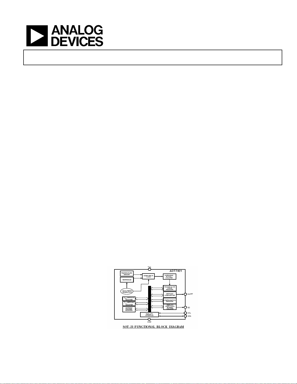
FUNCTIONAL BLOCK DIAGRAM
Figure 1. SOT-23 Functional Block Diagram
Rev. PrE
Information furnished by Analog Devices is believed to be accurate and reliable.
However, no responsibility is assumed by Analog Devices for its use, nor for any
infringements of patents or other rights of third parties that may result from its use.
Specifications subject to change without notice. No license is granted by implication
or otherwise under any patent or patent rights of Analog Devices. Trademarks and
registered trademarks are the property of their respective owners.
One Technology Way, P.O. Box 9106, Norwood, MA 02062-9106, U.S.A.
Tel: 781.329.4700 www.analog.com
Fax: 781.326.8703 © 2004 Analog Devices, Inc. All rights reserved.
Page 2

ADT7401 Preliminary Technical Data
TABLE OF CONTENTS
Specifications..................................................................................... 3
Application Hints ........................................................................... 10
Timing Characteristics..................................................................... 4
Absolute Maximum Ratings............................................................ 5
ESD Caution.................................................................................. 5
Pin Configuration and Function Descriptions............................. 6
Typical Performance Curves ........................................................... 7
Circuit Information...................................................................... 9
Converter Details.......................................................................... 9
Thermal Response Time ........................................................... 10
Self-Heating Effects.................................................................... 10
Supply Decoupling ..................................................................... 10
Temperature Monitoring........................................................... 10
Outline Dimensions ....................................................................... 11
Ordering Guide .......................................................................... 12
Rev. PrE | Page 2 of 12
Page 3

Preliminary Technical Data ADT7401
SPECIFICATIONS
All specifications apply for -40°C to +150°C unless otherwise stated. TA = T
Table 1.
Parameter Min Typ Max Units Test Conditions/Comments
TEMPERATURE SENSOR AND ADC
Accuracy @ VDD= +3.3 V (±10%) ±0.5 °C TA= 25°C.
±1 °C TA= 0°C to 70°C.
±2 °C TA= -40°C to +85°C.
±3 °C TA= -40°C to +125°C.
±4
1
°C TA= -40°C to +150°C.
Accuracy @ VDD= +5 V (±10%) ±0.5 °C TA= 25°C.
±1 °C TA= 0°C to 70°C.
±2 °C TA= -40°C to +85°C.
±3 °C TA= -40°C to +125°C.
±41 °C TA= -40°C to +150°C.
Temperature Resolution 0.0625 °C Equivalent to 12 Bits Sigma Delta ADC
Temperature Conversion Time 200 ms
Temperature Update Rtae 1 s Time between each conversion
Long Term Drift 0.25 °C Drift over 10 years if part is operated at +55°C.
Power Supply Rejection Ratio 0.3 0.6 °C/V TA= +25°C
DIGITAL INPUTS2
Input Current ± 1 µA VIN= 0 V to VDD
VIL, Input Low Voltage 0.3×VDD V
VIH, Input High Voltage 0.7×VDD V
Pin Capacitance 3 10 pF All digital inputs
SCL, SDA Glitch Rejection 50 ns Input filtering suppresses noise spikes of less than 50 ns.
DIGITAL OUTPUTS2
VOH, Ouput High Voltage 2.4 V I
VOL, Output Low Voltage 0.4 V IOL= 3 mA
IOH, Output High Current 1 mA VOH= 5 V
C
, Output Capacitance 50 p F
OUT
SUPPLIES
Supply Voltage 2.7 5.5 V
Supply Current Serial Bus Inactive.
Normal Mode6@ 3.3 V 230 450 µA Device Converting.
Normal Mode6@ 5 V 300 500 µA Device Converting.
Quiescent6@ 3.3 V 3 8 µA Device not converting.
Quiescent6@ 5.5 V 5 10 µA Device not converting.
One Shot Mode @ 1 sps 21.16 µA Average Current @ VDD= 2.7 V to 3.6 V.
One Shot Mode @ 1 sps 28.6 µA Average Current @ VDD= 4.5 V to 5.5 V.
Shutdown Current 0.3 1 µA
Power Dissipation 759 µW VDD= +3.3 V, Continuously Converting
Power Dissipation
1 sps 69.83 µW Average Power Dissipated for
V
1 sps 143 µ W Average Power Dissipated for
V
1
It is not recommended to operate the device at temperatures above +125°C for greater than a total of 5% of the lifetime of the device. Any exposure beyond this limit
will affect device reliability.
2
Guaranteed by design and characterization, not production tested.
MIN
to T
SOURCE
, VDD = +2.7 V to +5.5 V, unless otherwise noted
MAX
= I
= 200 µA
SINK
= +3.3 V. One Shot Mode.
DD
= +5 V. One Shot Mode.
DD
Rev. PrE | Page 3 of 12
Page 4
ADT7401 Preliminary Technical Data
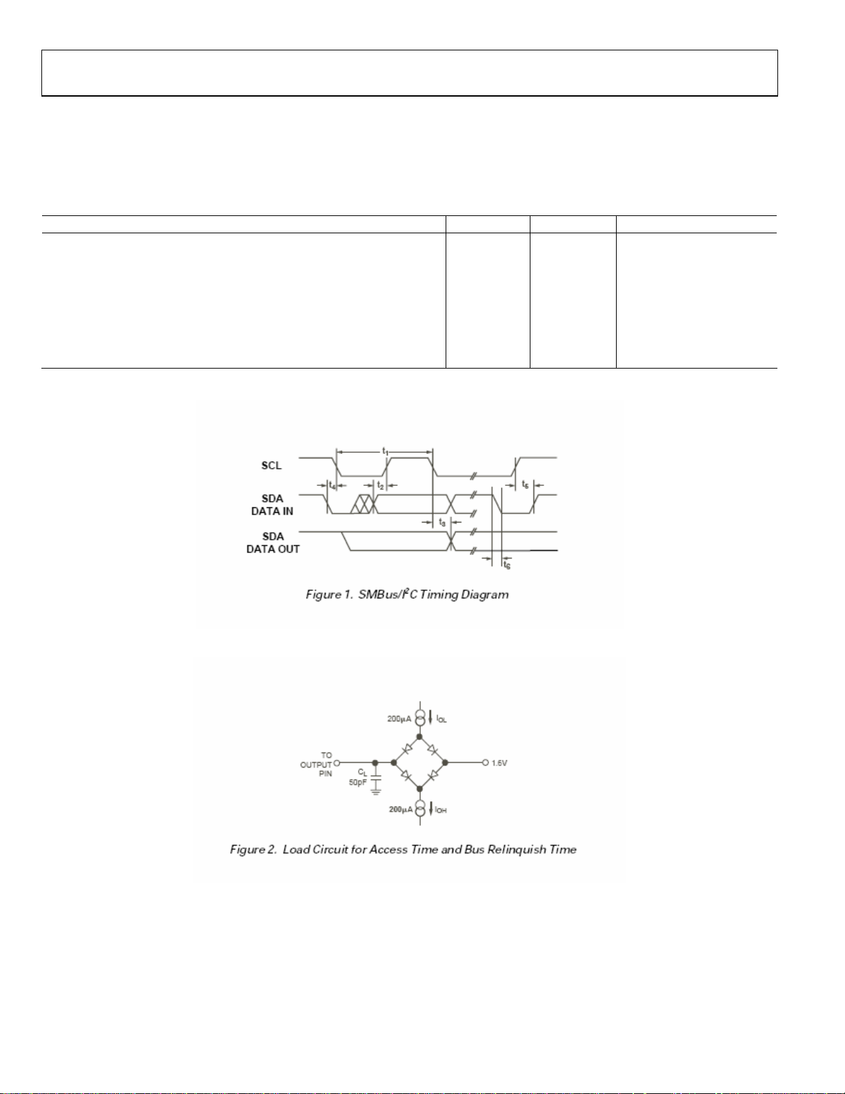
TIMING CHARACTERISTICS
Guaranteed by design and characterization, not production tested. The SDA & SCL timing is measured with the input filters turned on so
as to meet the Fast-Mode I
behaviour of the part. T
Table 2.
Parameter Limit Units Comments
Serial Clock Period, t1 2.5 µs Fast Mode I2C. See Figure 2
Data In Setup Time to SCL High, t2 50 ns
Data Out Stable after SCL Low, t3 0 ns See Figure 2
SDA Low Setup Time to SCL Low
(Start Condition), t4 50 ns See Figure 2
SDA High Hold Time after SCL High
(Stop Condition), t5 50 ns See Figure 2
SDA and SCL Fall Time, t6 90 ns See Figure 2
2
C specification. Switching off the input filters improves the transfer rate but has a negative affect on the EMC
= T
to T
A
MIN
, VDD = +2.7 V to +5.5 V, unless otherwise noted.
MAX
2
Figure 2. SMBus/I
Figure 3. Load Circuit for Access Time and Bus Relinquish Time
C Timing Diagram
Rev. PrE | Page 4 of 12
Page 5

Preliminary Technical Data ADT7401
ABSOLUTE MAXIMUM RATINGS
Table 3.
Parameter Rating
VDD to GND –0.3 V to +7 V
Digital Input Voltage to GND –0.3 V to VDD + 0.3 V
Maximum Output Current (OUT) ±10 mA
Operating Temperature Range3 –40°C to +150°C
Storage Temperature Range –65°C to +160°C
Max Junction Temperature, T
+150°C
JMAX
6-Lead SOT-23
Power Dissipation
Thermal Impedance
4
6
θJA, Junction-to-Ambient
(still air)
W
= (T
MAX
229.6°C/W
JMAX
- T
5
)/θ
A
JA
θJC, Junction-to-Case 91.99°C/W
8-Lead MSOP (RM-8)
Power Dissipation2 W
MAX
= (T
JMAX
- T
3
)/θ
A
JA
Thermal Impedance4
θJA, Junction-to-Ambient
(still air)
205.9°C/W
θJC, Junction-to-Case 43.74°C/W
IR Reflow Soldering
Peak Temperature +220°C (-0/+5°C)
Time at Peak Temperature 10 to 20 secs
Ramp-up Rate 2-3°C/sec
Ramp-down Rate –6°C/sec
3
It is not recommended to operate the device at temperatures above +125°C
for greater than a total of 5% of the lifetime of the device. Any exposure
beyond this limit will affect device reliability.
4
Values relate to the package being used on a 2-layer PCB. See . for a
plot of max power dissipation vs. ambient temperature (T
5
TA = Ambient Temperature.
6
Junction-to-Case resistance is applicable to components featuring a
preferential flow direction, e.g. components mounted on a heat sink.
Junction-to-Ambient resistance is more useful for air-cooled PCB mounted
components.
Figure 4
).
A
Stresses above those listed under Absolute Maximum Ratings
may cause permanent damage to the device. This is a stress
rating only; functional operation of the device at these or any
other conditions above those indicated in the operational
section of this specification is not implied. Exposure to absolute
maximum rating conditions for extended periods may affect
device reliability.
Figure 4. Plot of Maximum Power Dissipation vs. Temperature
ESD CAUTION
ESD (electrostatic discharge) sensitive device. Electrostatic charges as high as 4000 V readily accumulate on
the human body and test equipment and can discharge without detection. Although this product features
proprietary ESD protection circuitry, permanent damage may occur on devices subjected to high energy
electrostatic discharges. Therefore, proper ESD precautions are recommended to avoid performance
degradation or loss of functionality.
Rev. PrE | Page 5 of 12
Page 6

ADT7401 Preliminary Technical Data
PIN CONFIGURATION AND FUNCTION DESCRIPTIONS
Figure 5. Pin Configurations
Table 4. Pin Function Description
SOT-23
Mnemonic
SDA 6 1 SMBus/I2C Serial Data Input/Output. Open-drain configuration needs a pullup resistor.
SCL 5 2 Serial clock input. Open-drain configuration.
ALERT 4 3
GND 3 4 Analog and Digital Ground.
DC 2 7
VDD 1 8 Positive Supply Voltage, 2.7 V to 5.5 V.
A0 - 5 Digital Input. User set programmable bit of the serial bus address.
A1 - 6 Digital Input. User set programmable bit of the serial bus address.
Pin No.
MSOP
Pin No.
Description
Digital open-drain output. Out of limit temperature indicator. This output becomes active when
or T
temperature exceeds T
Daisy Chain Digital Input/Output. This pin acts as the input/output conduit for the sub-SMBus/I
bus. Push-Pull configuration.
HIGH
limits. Can be programmed to be active low or active high
LOW
2
C
Rev. PrE | Page 6 of 12
Page 7

Preliminary Technical Data ADT7401
TYPICAL PERFORMANCE CURVES
Figure 6. Supply Current vs. Supply Voltage @ +25°C
Figure 8. PSRR vs. Supply Ripple Frequency
Figure 7. Shutdown Current vs. Supply Voltage @ +25°C
Rev. PrE | Page 7 of 12
Figure 9. Temperature Error at 3.3 V and 5 V
Page 8

ADT7401 Preliminary Technical Data
Figure 10. Temperature Error vs. Power Supply Noise Frequency
Figure 11. Temperature Sensor Response to Thermal Shock
Figure 12. Supply Current vs. Temperature
Figure 13. Power Supply Rejection vs. Temperature
Rev. PrE | Page 8 of 12
Page 9

Preliminary Technical Data ADT7401
CIRCUIT INFORMATION
The ADT7401 is a standalone temperature sensor that generates
a 12-bit digital output in two’s complement that varies in direct
proportion with the temperature of the device. An onboard
sensor generates a voltage precisely proportional to absolute
temperature which is compared to an internal voltage reference
and input to a precision digital modulator. The serial digital
output is converted into a 12-bit digital word and stored in the
Temperature Value Register. Overall accuracy is ±5°C from 0°C
to +70°C, with excellent transducer linearity. The digital output
of the ADT7401 is SMBus/I
interfaced to most popular microcontrollers.
The onboard temperature sensor has excellent accuracy and
linearity over the entire rated temperature range without
correction or calibration by the user.
The sensor output is digitized by a first-order sigma-delta
modulator, also known as the “charge balance” type analog-todigital converter. This type of converter utilizes time-domain
oversampling and a high accuracy comparator to deliver 12 bits
of effective accuracy in an extremely compact circuit.
2
C compatible, and is easily
cycle of the comparator output in response to input voltage
changes. The comparator samples the output of the integrator at
a much higher rate than the input sampling frequency, this is
called oversampling. This spreads the quantization noise over a
much wider band than that of the input signal, improving
overall noise performance and increasing accuracy.
Figure 14. First-Order Sigma-Delta Modulator
CONVERTER DETAILS
The sigma-delta modulator consists of an input sampler, a
summing network, an integrator, a comparator, and a 1-bit
DAC. Similar to the voltage-to-frequency converter, this
architecture creates in effect a negative feedback loop whose
intent is to minimize the integrator output by changing the duty
The modulated output of the comparator is encoded using a
circuit technique, which results in a serial digital signal. This
signal is then converted into a 12-bit digital word for storage
into a register. The final output format is two’s complement.
Rev. PrE | Page 9 of 12
Page 10

ADT7401 Preliminary Technical Data
APPLICATION HINTS
THERMAL RESPONSE TIME
The time required for a temperature sensor to settle to a
specified accuracy is a function of the thermal mass of, and the
thermal conductivity between, the sensor and the object being
sensed. Thermal mass is often considered equivalent to
capacitance. Thermal conductivity is commonly specified using
the symbol θ, and can be thought of as thermal resistance. It is
commonly specified in units of degrees per watt of power
transferred across the thermal joint. Thus, the time required for
the ADT7401 to settle to the desired accuracy is dependent on
the package, the thermal contact established in that particular
application, and the equivalent power of the heat source. In
most applications, the settling time is probably best determined
empirically.
SELF-HEATING EFFECTS
The temperature measurement accuracy of the ADT7401 may
be degraded in some applications due to self-heating. Errors
introduced are from the quiescent dissipation and power
dissipated when converting. The magnitude of these
temperature errors is dependent on the thermal conductivity of
the ADT7401 package, the mounting technique, and effects of
airflow. Static dissipation in the ADT7401 is typically 10 µW
operating at 3.3 V with no load. In the 6 lead SOT-23 package
mounted in free air, this accounts for a temperature increase
due to self-heating of:
CWCWθPT
°=°×µ=×=∆ 0328.0/6.229143
JADISS
It is recommended that current dissipated through the device is
kept to a minimum as it has a proportional affect on the
temperature error.
SUPPLY DECOUPLING
The ADT7401 should be decoupled with a 0.1 µF ceramic
capacitor between V
if the ADT7401 is mounted remote from the power supply.
Precision analog products, such as the ADT7401, require a well
filtered power source. Since the ADT7401 operates from a
single supply, it seems convenient to simply tap into the digital
logic power supply. Unfortunately, the logic supply is often a
switch-mode design, which generates noise in the 20 kHz to 1
MHz range. In addition, fast logic gates can generate glitches
hundred of millivolts in amplitude due to wiring resistance and
and GND. This is particularly important
DD
inductance.
If possible, the ADT7401 should be powered directly from the
system power supply. This arrangement, shown in Figure 15,
will isolate the analog section from the logic switching
transients. Even if a separate power supply trace is not available,
however, generous supply bypassing will reduce supply-line
induced errors. Local supply bypassing consisting of a 0.1 µF
ceramic capacitor is recommended.
Figure 15. Use Separate Traces to Reduce Power Supply Noise
TEMPERATURE MONITORING
The ADT7401 is ideal for monitoring the thermal environment
within electronic equipment. For example, the surface mounted
package will accurately reflect the exact thermal conditions
which affect nearby integrated circuits.
The ADT7401 measures and converts the temperature at the
surface of their own semiconductor chip. When the ADT7401 is
used to measure the temperature of a nearby heat source, the
thermal impedance between the heat source and the ADT7401
must be considered. Often, a thermocouple or other
temperature sensor is used to measure the temperature of the
source while the ADT7401’s temperature is monitored. Once
the thermal impedance is determined, the temperature of the
heat source can be inferred from the ADT7401 output.
One example of using the ADT7401’s unique properties is in
monitoring a high power dissipation microprocessor. The
adt7401, in a surface mount package, is mounted directly
beneath the microprocessor’s pin grid array (PGA) package.
Rev. PrE | Page 10 of 12
Page 11

Preliminary Technical Data ADT7401
OUTLINE DIMENSIONS
Figure 16. 6-Lead Plastic Surface Mount SOT-23
RT-6)
Dimensions shown in Millimeters
Figure 17. 8-Lead Plastic Surface Mount Mini/Micro SOIC (MSOP)
(RM-8)
Dimensions shown in Millimeters
Rev. PrE | Page 11 of 12
Page 12

ADT7401 Preliminary Technical Data
ORDERING GUIDE
Temperature
Model
ADT7401RT500REEL7
Range1
-40°C to +150°C ±1°C 6-Lead SOT-23 RJ-6 500
ADT7401RT-REEL -40°C to +150°C ±1°C 6-Lead SOT-23 RJ-6 10000
ADT7401RT-
REEL7
ADT7401RM-
500REEL7
ADT7401RM-
REEL
ADT7401RM-
REEL7
-40°C to +150°C ±1°C 6-Lead SOT-23 RJ-6 3000
-40°C to +150°C ±1°C 8-Lead MSOP RM-8 500
-40°C to +150°C ±1°C 8-Lead MSOP RM-8 10000
-40°C to +150°C ±1°C 8-Lead MSOP RM-8 3000
Temperature
Accuracy2
Package
Description
Branding
Information
Package
Option
Minimum
Quantities/Reel
2
Purchase of licensed I
purchaser under the Philips I
C components of Analog Devices or one of its sublicensed Associated Companies conveys a license for the
2
C Patent Rights to use these components in an I2C system, provided that the system conforms to the I2C
Standard Specification as defined by Philips.
1
It is not recommended to operate the device at temperatures above +125°C for greater than a total of 5% of the lifetime of the device. Any exposure beyond this limit
will affect device reliability.
2
Temperature accuracy is over 0°C to +70°C temperature range.
© 2004 Analog Devices, Inc. All rights reserved. Trademarks and
registered trademarks are the property of their respective companies.
PR04792-0-3/04(PrE)
Rev. PrE | Page 12 of 12
 Loading...