

Page 1
SHARC® Mel-100
SUMMARY
High performance 32-bit audio processor
Super Harvard Architecture Computer (SHARC)
4 independent buses for dual data, instruction, and
nonintrusive, zero-overhead I/O fetch on a single cycle
Code compatible with all other SHARC family DSPs
Single-instruction-multiple-data (SIMD) computational
architecture—two 32-bit IEEE floating-point computation units, each with a multiplier, ALU, shifter, and
register file
CORE PROCESSOR
INSTRUCTION
CACHE
32 × 48-BIT
PROGRAM
SEQUENCER
32
32
64
64
BARREL
SHIFTER
DAG1
8 × 4 × 32
BUS
CONNECT
(PX)
MULT
DAG2
8 × 4 × 32
DATA
REGISTER
FILE
(PEX)
16 × 40-BIT
TIMER
PM ADDRESS BUS
DM ADDRESS BUS
PM DATA BUS
DM DATA BUS
BARREL
SHIFTER
ADSST-SHARC-Mel-100
2
Serial ports offer I
simultaneous receive or transmit pins, which support up
to 16 transmit or 16 receive channels of audio
Integrated peripherals—integrated I/O processor,
0.5 Mbit on-chip SRAM, SDRAM controller, glueless
multiprocessing features, and I/O ports (serial, link,
external bus, SPI®, and JTAG)
SHARC Mel-100 supports 32-bit fixed-point, 32-bit
floating-point, and 40-bit floating-point formats
DUAL-PORTED SRAM
TWO INDEPENDENT
DUAL-PORTED BLOCKS
PROCESSOR PORT
ADDR DATA ADDR
ADDR DATA
DATA
REGISTER
FILE
(PEY)
16 × 40-BIT
MULT
S support via 8 programmable and
I/O PORT
DATA
DATA
IOD
64
Audio Processor
6
12
8
24
32
ADDR
IOA
18
BLOCK 0
BLOCK 1
JTAG
TEST & EMULATION
GPIO
FLAGS
SDRAM
CONTROLLER
EXTERNAL PORT
ADDR BUS
MUX
MULTIPROCESSOR
INTERFACE
DATA BUS
MUX
HOST PORT
ALU
ALU
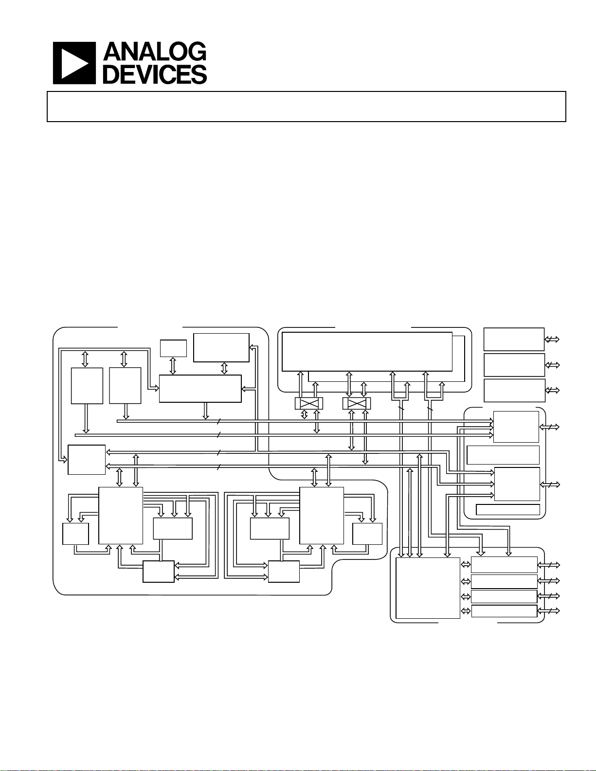
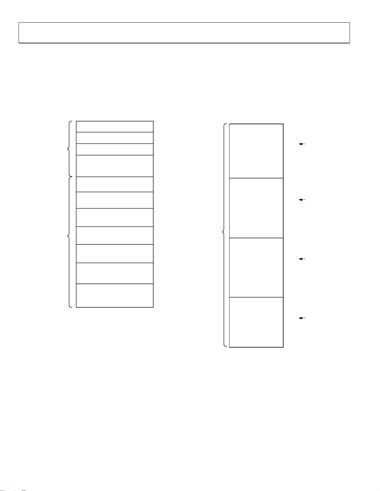
Figure 1. Functional Block Diagram
Rev. 0
Information furnished by Analog Devices is believed to be accurate and reliable.
However, no responsibility is assumed by Analog Devices for its use, nor for any
infringements of patents or other rights of third parties that may result from its use.
Specifications subject to change without notice. No license is granted by implication
or otherwise under any patent or patent rights of Analog Devices. Trademarks and
registered trademarks are the property of their respective owners.
IOP
REGISTERS
(MEMORY MAPPED)
CONTROL,
STATUS, AND
DATA BUFFERS
I/O PROCESSOR
One Technology Way, P.O. Box 9106, Norwood, MA 02062-9106, U.S.A.
Tel: 781.329.4700
Fax: 781.326.8703 © 2003 Analog Devices, Inc. All rights reserved.
www.analog.com
DMA
CONTROLLER
SERIAL PORTS (4)
LINK PORTS (2)
SPI PORTS (1)
5
16
20
4
Page 2

ADSST-SHARC-Mel-100
TABLE OF CONTENTS
Key Features ...................................................................................... 3
Absolute Maximum Ratings ......................................................... 20
General Description......................................................................... 4
Hardware Architecture ................................................................ 4
Software Architecture .................................................................. 5
SHARC Mel-100 Family Core Architecture.............................. 6
SHARC Mel-100 Memory and I/O Interface Features............ 9
Pin Function Descriptions ............................................................ 12
Boot Modes .................................................................................17
Specifications................................................................................... 18
Recommended Operating Conditions .................................... 18
Electrical Characteristics........................................................... 19
REVISION HISTORY
Revision 0: Initial Version
Timing Specifications ................................................................ 20
Power Dissipation ...................................................................... 21
Output Drive Currents .............................................................. 21
Test Conditions........................................................................... 21
Environmental Conditions ....................................................... 23
Pin Configuration........................................................................... 24
Pin Layout Summary ................................................................. 25
Outline Dimensions....................................................................... 26
Ordering Guide .......................................................................... 26
Rev. 0 | Page 2 of 28
Page 3

ADSST-SHARC-Mel-100
KEY FEATURES
100 MHz (10 ns) core instruction rate
Single-cycle instruction execution, including SIMD
operations in both computational units
600 Mflops peak and 400 Mflops sustained performance
225-ball 17 mm × 17 mm MBGA package
Decodes industry-standard formats, using a 32-bit floatingpoint implementation
Decoders:
Dolby® Digital, Dolby Pro Logic® II, DTS-ES® Extended
Surround (including DTS-ES Discrete and DTS-ES
Matrix), DTS-96/24, DTS Neo:6®
PCM
Delay management
Bass management
MPEG-2 AAC
Wavesurround® virtual headphone and virtual
loudspeaker
Downsampling 96 kHz to 48 kHz (2-channel)
Single-chip DSP based implementation of digital audio
algorithms
SHARC Mel-100 processor features 100 MIPS
2
S compatible serial ports
I
Interface to external SDRAM
Easy interfaces to audio codecs
192 kHz processing
Supports customer specific postprocessing
Automatic stream detection
Automatic code loading
Easy to use software architecture
Optimized library of routines
Host communication using SPI port
Supports IEC 60958 for bit streams
8-channel output
Rev. 0 | Page 3 of 28
Page 4
ADSST-SHARC-Mel-100
GENERAL DESCRIPTION
The SHARC Mel-100 family of powerful 32-bit audio
processors from Analog Devices enables flexible designs and
delivers a host of features across high-end and high fidelity
audio systems to the AV receiver and DVD markets. It includes
multichannel audio decoders, encoders, and postprocessors for
digital audio designs using DSPs in home theater systems and
automotive audio receivers.
With 32-bit audio quality, the SHARC Mel-100 audio processor
autodetects and decodes audio formats in real time, enabling
end users to enjoy a theater-quality audio experience in their
homes and automobiles.
The designs can be customized to meet the exact requirements
of the application. This audio DSP system enables designers to
make value additions to product features working off the highend base functionality with which they are provided.
Evaluation boards, sample applications, and all necessary
software support (e.g., drivers) are available. The evaluation
board enables OEMs to offer comprehensive and single-chip
implementations of advanced features for end-user products.
SHARC Mel-100 audio processors enable OEMs to produce
high quality, low cost designs featuring decoder algorithms and
postprocessors for DTS-ES Extended Surround (including both
DTS Discrete 6.1 and DTS Matrix 6.1), DTS Neo:6, Dolby
Digital, Dolby Pro Logic II, AAC, and WaveSurround.
The cost of development is reduced, enabling common
solutions across product lines. Field and remotely upgradeable
products with programmable DSPs and an optimized library of
routines, along with the best development tools in the industry,
reduce the time to market.
HARDWARE ARCHITECTURE
Hardware architecture includes the interface between the DSP
and the host microcontroller, command processing, data
transfer in serial and parallel form, data buffer management,
algorithm combinations, MIPS, and memory requirements that
are provided.
The multichannel algorithms are implemented on a SHARC
Mel-100 AVR evaluation board. The board is standalone and
accepts a compressed digital bit stream as serial input from
LD/DVD/CD players or stream generators, decodes the bit
stream, and generates a PCM stream in real time in
2-channel or multichannel mode. It has a microcontroller to
handle commands and option selections from a small keypad
and an LCD display for status display.
SDRAM
128k × 32,
BOOT ROM
1M × 8
IRQ
GPIO
ADC
SERIAL PORT
DAC
S/PDIF
TRANSMITTER
S/PDIF
RECEIVER
MULTI-
CHANNEL
CODEC
COMMAND
KERNEL
SHARC Mel-100 is the comprehensive answer to the needs of
the high-end, high quality digital audio market. It delivers a
realistic high fidelity audio experience along with the maximum
number of features in the product, across price points in the
high-end home theater and DVD markets.
Rev. 0 | Page 4 of 28
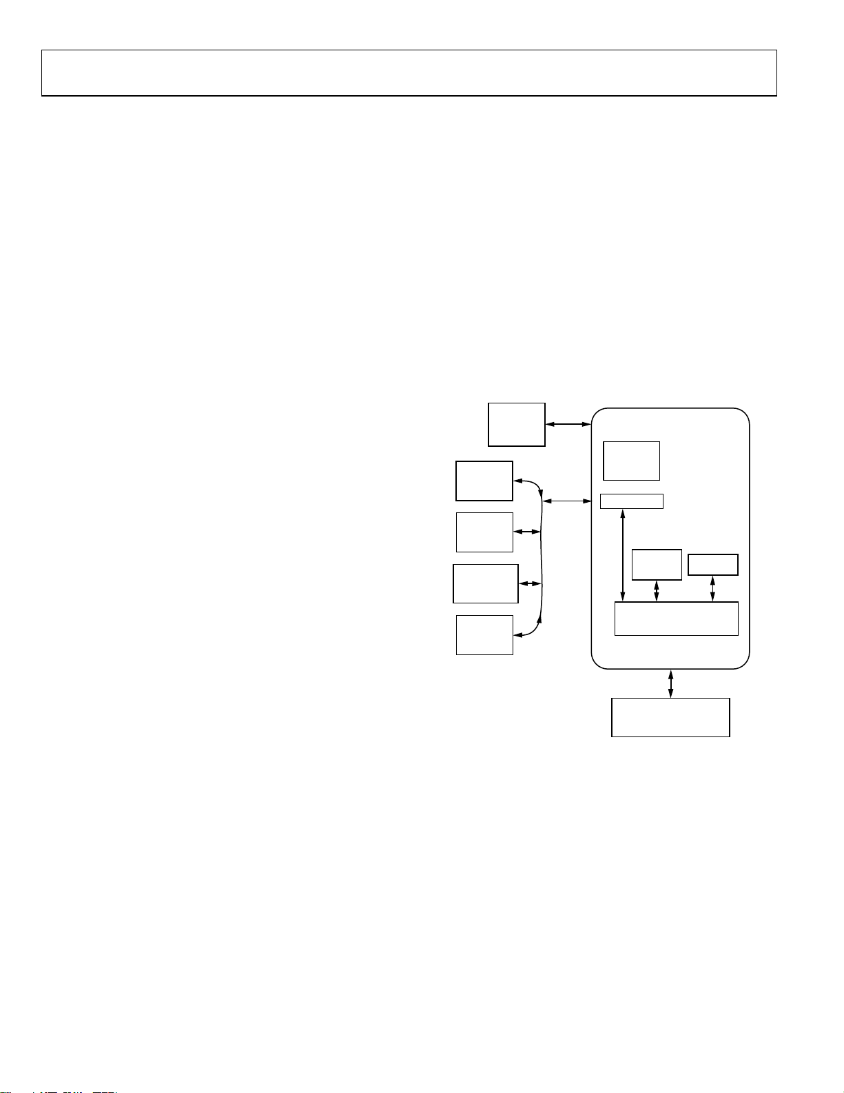
HOST MICRO
03373-0-002
Figure 2. Simplified Block Diagram
To understand the SHARC Mel-100 family hardware
architecture, one should examine its four major blocks:
• The Core Processor
• Dual-Ported SRAM
• External Port
• Input/Output Processor
The hardware architecture of the SHARC Mel-100 is complex. It
has four independent buses for dual data, one for instructions,
and one for I/O fetch. Since the four buses are independent,
multiple transactions take place within a single clock cycle. It
has two external ports, DMA channels, and eight serial ports. It
is a 0.35 ns technology IC operating at 3.3 V.
Page 5

ADSST-SHARC-Mel-100
The SHARC Mel-100 processor can be interfaced to external
peripherals with relative ease. The communication between the
SHARC Mel-100 processor and a host microcontroller utilizes
the SPI bus. The host microcontroller can be the master and the
SHARC Mel-100 processor can act as a slave. The peripherals
can be controlled by the host microcontroller using the SPI bus.
The communication is based on commands and parameters.
Status information regarding the SHARC Mel-100 decoding is
periodically updated and made available to the host
microcontroller.
The block diagram of the SHARC Mel-100 (see Figure 1)
illustrates the following architectural features:
• Computation units (ALU, multiplier, and shifter) with a
shared data register file
• Data address generators (DAG1, DAG2)
• Program sequencer with instruction cache
• Timers with event capture modes
• On-chip, dual-ported SRAM
• External port for interfacing to off-chip memory and
peripherals
• Host port and SDRAM interface
• DMA controller
• Enhanced serial ports
• JTAG test access port
We will use Figure 2 as our reference. The SHARC Mel-100
communicates with the host microcontroller using SPI. The
SHARC Mel-100 has an on-chip memory buffer that is used for
storing commands/parameters sent by the host to the SHARC
Mel-100 and also status information from the SHARC Mel-100.
There is a defined protocol for passing commands and
obtaining status information. Once the SHARC Mel-100
receives a command from the host micro, it will process the
command and inform the host micro about the status. These
commands initiate actions such as encoding and decoding.
Encoding and decoding will result in data processing and the
processed data may be delivered over the serial port. For
example, while encoding, the MP3 data is accepted through the
serial port from peripherals like an ADC or S/PDIF receiver.
The MP3 data is then encoded and stored in an on-chip
compressed data buffer. The SHARC Mel-100 will prepare the
compressed frames in IEC 958 format so that they can be sent
out using the serial port or S/PDIF transmitter. Using the serial
port, compressed frames can be downloaded to the SHARC
Mel-100, where they can be decoded, and the resulting MP3
data can be sent on the serial port transmitter. While commands
and data are transferred between the host microcontroller and
the SHARC Mel-100 over the SPI, reliable communication
needs the help of interrupts and a few general-purpose
input/output lines.
SOFTWARE ARCHITECTURE
The audio processors from Analog Devices enable designers to
make value additions to product features working off the highend base functionality. The SHARC Mel-100 software has the
following parts:
• Executive kernel
• Algorithm as library module
The executive kernel has the following functions:
• Power-up hardware initialization
• Serial port management
• Automatic stream detect
• Automatic code load
• Command processing
• Interrupt handling
• Data buffer management
• Calling library module
• Status report
The executive kernel gets executed as soon as booting takes
place. The hardware resources are initialized in the beginning.
The command buffer and general-purpose programmable flag
pins are initialized. Various data buffers and memory variables
are initialized. Interrupts are programmed and enabled. Then,
definite signatures are written “Command buffer” to inform the
host that the SHARC Mel-100 is ready to receive the
commands. Once commands are issued by the host
microcontroller, they are executed and appropriate actions take
place. Decoding is handled by issuing appropriate commands
from the host microcontroller.
The kernel communicates with the library module for a
particular algorithm in a defined way. The details are found in
the specific implementation documents. As the kernel is
modular, it is easy to customize to different hardware platforms.
Most of the time, users need to change the initialization code to
suit the particular codec chosen.
INPUT STREAM
DECODING
LIBRARY
EXECUTIVE KERNEL
Figure 3. Software
The SHARC Mel-100 includes a 100 MHz core, dual-ported onchip SRAM, an integrated I/O processor with multiprocessing
support, and multiple internal buses to eliminate I/O
bottlenecks. The SHARC Mel-100 offers a Single-InstructionMultiple-Data (SIMD) architecture, using two computational
units. Fabricated in a state-of-the-art, high speed, low power
CMOS process, the SHARC Mel-100 has a 10 ns instruction
cycle time.
OUTPUT STREAM
Rev. 0 | Page 5 of 28
Page 6
ADSST-SHARC-Mel-100
With its SIM
the SHARC Mel-100 can perform 600 million math operations
per second. Table 1 shows performance benchmarks for the
SHARC Mel-100.
The SHARC Mel-1
standards of integration for DSPs, combining a high
performance 32-bit DSP core with integrated, on-chip system
features. These features include a 1-Mbit dual-ported SRAM
memory, a host processor interface, an I/O processor that
supports 14 DMA channels, four serial ports, two link ports, a
SDRAM controller, an SPI interface, an external parallel bus,
and glueless multiprocessing.
Figure 2 illustrates the followin
• Two processing elements, each made up of an AL
• Data address generators (DAG1, DAG2)
• Program sequencer with instruction cach
• PM and DM buses capable of supporting fo
•
• On-chip SRAM
• SDRAM controller for gluel
• External port that supports
• D
• Four serial ports
• Two link p o r ts
• SPI compatible
• JTAG test access port
• 12 general-purpose I/O
Figure 4 shows a typical single-p
multiprocessing system appears in Figure 8.
D computational hardware running at 100 MHz,
00 continues the SHARC’s industry-leading
g architectural features:
U,
multiplier, shifter, and data register file
e
ur 32-bit
data transfers between memory and the core every co
processor cycle
Interval timer
(0.5 Mbit)
ess interface to SDRAMs
• Interfacing to off-chip me
mory peripherals
• Glueless multiprocessing for six SHARC Mel-1
processors
• Host port read/write of IOP registers
MA controller
interface
pins
rocessor system. A
re
00
SHARC MEL-100 FAMILY CORE ARCHITECTURE
The SHARC Mel-100 includes the following architectural
features of the ADSP-2116x family core:
SIMD Computational Engine
The SHARC Mel-100 contains two computational processing
elements that operate as a Single Instruction Multiple Data
(SIMD) engine. The processing elements are referred to as PEX
and PEY, and each contains an ALU, multiplier, shifter, and
n
register file. PEX is always active, and PEY may be enabled by
setting the PEYEN mode bit in the MODE1 register. When this
mode is enabled, the same instruction is executed in both
processing elements, but each processing element operates on
different data. This architecture is efficient at executing mathintensive DSP algorithms.
Entering SIMD mode also has an effect on the way data is
transferred between memory and the processing elements.
When in SIMD mode, twice the data bandwidth is required to
sustain computational operation in the processing elements.
Because of this requirement, entering SIMD mode also doubles
the bandwidth between memory and the processing elements.
When using the DAGs to transfer data in SIMD mode, two data
values are transferred with each access of memory or the
register file.
Independent, Parallel Computation Units
Within each processing element is a set of computational units.
The computational units consist of an arithmetic/logic unit
(ALU), multiplier, and shifter. These units perform single-cycle
instructions. The three units within each processing element are
arranged in parallel, maximizing computational throughput.
Single multifunction instructions execute parallel ALU and
multiplier operations. In SIMD mode, the parallel ALU and
multiplier operations occur in both processing elements. These
computation units support IEEE 32-bit single-precision
floating-point, 40-bit extended precision floating-point, and
32-bit fixed-point data formats.
Table 1. Benchmarks (at 100 MHz)
Benchmark Algorithm Speed (at 100 MHz)
1024 Point Complex FFT
(Radix 4, with Reversal)
FIR Filter (per Tap)1 5 ns
IIR Filter (per Biquad)1 40 ns
Matrix Multiply (Pipelined)
[3 × 3] • [3 × 1] 30 ns
[4 × 4] • [4 × 1] 37 ns
Divide (y/x) 60 ns
Inverse Square Root 40 ns
DMA Transfers 800 Mbytes/s
1
Assumes two filters in multichannel SIMD mode
1
171 µs
Rev. 0 | Page 6 of 28
Page 7
ADSST-SHARC-Mel-100
ADSST SHARC
MEL-100
3
12
2
CLKIN
XTAL
CLK_CFG1–0
CLKDBL
EBOOT
LBOOT
IRQ2-0
FLAG11–0
TIMEXP
RPBA
ID2-0
LXCLK
LXACK
LXDAT7–0
SCLK0
FS0
D0A
D0B
SCLK1
FS1
D1A
D1B
SCLK2
FS2
D2A
D2B
SCLK3
FS3
D3A
D3B
SPICLK
SPIDS
MOSI
MISO
RESET
RSTOUT
BMS
BRST
ADDR23–0
DATA47–16
WR
ACK
MS3–0
RAS
CAS
DQM
SDWE
SDCLK1–0
SDCKE
SDA10
CLKOUT
DMAR1–2
DMAG1–2
HBR
HBG
REDY
BR1–6
SBTS
JTAG
RD
CS
PA
7
CONTROL
Figure 4. System Block Diagram
ADDRESS
DATA
CS
ADDR
DATA
ADDR
DATA
OE
WE
ACK
CS
DATA
ADDR
DATA
BOOT
EPROM
(OPTIONAL)
MEMORY
AND
PERIPHERALS
(OPTIONAL)
DMA DEVICE
(OPTIONAL)
HOST
PROCESSOR
INTERFACE
(OPTIONAL)
03681-0-001
RAS
CAS
DQM
WE
CLK
CKE
A10
CS
ADDR
DATA
SDRAM
(OPTIONAL)
Instruction Cache
The SHARC Mel-100 includes an on-chip instruction cache that
enables 3-bus operation for fetching an instruction and four
data values. The cache is selective—only the instructions whose
fetches conflict with PM bus data accesses are cached. This
cache enables full speed execution of core, looped operations
such as digital filter multiply-accumulates and FFT butterfly
processing.
Data Address Generators with Hardware Circular Buffers
The SHARC Mel-100 processor’s two data address generators
(DAGs) are used for indirect addressing and implementing
circular data buffers in hardware. Circular buffers enable
efficient programming of delay lines and other data structures
required in digital signal processing, and are commonly used in
digital filters and Fourier transforms. The two DAGs of the
SHARC Mel-100 contain sufficient registers to enable the
creation of up to 32 circular buffers (16 primary register sets,
16 secondary). The DAGs automatically handle address pointer
CLOCK
LINK
DEVICES
(2 MAX)
(OPTIONAL)
SERIAL
DEVICE
(OPTIONAL)
SERIAL
DEVICE
(OPTIONAL)
SERIAL
DEVICE
(OPTIONAL)
SERIAL
DEVICE
(OPTIONAL)
SPI
COMPATIBLE
DEVICE
(HOST OR SLAVE)
(OPTIONAL)
Data Register File
A general-purpose data register file is contained in each
processing element. The register files transfer data between the
computation units and the data buses, and store intermediate
results. These 10-port, 32-register (16 primary, 16 secondary)
register files, combined with the SHARC Mel-100’s enhanced
Harvard architecture, enable unconstrained data flow between
computation units and internal memory. The registers in PEX
are referred to as R0–R15, and in PEY as S0–S15.
Single-Cycle Fetch of Instruction and Four Operands
The SHARC Mel-100 features an enhanced Harvard
architecture in which the data memory (DM) bus transfers data
and the program memory (PM) bus transfers both instructions
and data (see Figure 4). With the SHARC Mel-100’s separate
program and data memory buses and on-chip instruction cache,
the processor can simultaneously fetch four operands (two over
each data bus) and an instruction (from the cache), all within a
single cycle.
Rev. 0 | Page 7 of 28
Page 8
ADSST-SHARC-Mel-100
Y
L
Y
wraparound, reduce overhead, increase performance, and
simplify implementation. Circular buffers can start and end at
any memory location.
Flexible Instruction Set
The 48-bit instruction word accommodates a variety of parallel
operations for concise programming. For example, the SHARC
Mel-100 can conditionally execute a multiply, an add, and a
ADDRESS
subtract in both processing elements, while branching, all
within a single instruction.
ADDRESS
INTERNA
MEMOR
SPACE
MULTIPROCESSOR
MEMOR
SPACE
IOP REGISTERS
LONG WORD ADDRESSING
NORMAL WORD ADDRESSING
SHORT WORD ADDRESSING
IOP REGISTERS OF
ADSST-SHARC-MEL-100
WITH ID = 001
IOP REGISTERS OF
ADSST-SHARC-MEL-100
WITH ID = 010
IOP REGISTERS OF
ADSST-SHARC-MEL-100
WITH ID = 011
IOP REGISTERS OF
ADSST-SHARC-MEL-100
WITH ID = 100
IOP REGISTERS OF
ADSST-SHARC-MEL-100
WITH ID = 101
IOP REGISTERS OF
ADSST-SHARC-MEL-100
WITH ID = 110
RESERVED
0x0000 0000–0x0001 FFFF
0x0002 0000–0x0002 1FFF (BLK 0)
0x0002 8000–0x0002 9FFF (BLK 1)
0x0004 0000–0x0004 3FFF (BLK 0)
0x0005 0000–0x0005 3FFF (BLK 1)
0x0008 0000–0x0008 7FFF (BLK 0)
0x000A 0000–0x000A 7FFF (BLK 1)
0x0010 0000–0x0011 FFFF
0x0012 0000–0x0013 FFFF
0x0014 0000–0x0015 FFFF
0x0016 0000–0x0017 FFFF
0x0018 0000–0x0019 FFFF
0x001A 0000–0x001B FFFF
0x001C FFFF
0x001F FFFF
0x0020 0000
MS0
BANK 0
0x00FF FFFF (NON-SDRAM)
0x03FF FFFF (SDRAM)
0x0400 0000
MS1
BANK 1
0x04FF FFFF (NON-SDRAM)
0x07FF FFFF (SDRAM)
0x0800 0000
MS2
BANK 2
0x08FF FFFF (NON-SDRAM)
0x0BFF FFFF (SDRAM)
0x0C00 0000
EXTERNAL MEMORY SPACE
BANK 3
0x0CFF FFFF (NON-SDRAM)
0x0FFF FFFF (SDRAM)
NOTE: BANK SIZES ARE FIXED
MS3
Figure 5. Memory Map Block Diagram
Rev. 0 | Page 8 of 28
Page 9
ADSST-SHARC-Mel-100
SHARC MEL-100 MEMORY AND I/O INTERFACE FEATURES
The SHARC Mel-100 adds the following architectural features
to the ADSP-2116x family core:
On-Chip Memory
The SHARC Mel-100 contains 0.5 Mbit of on-chip SRAM.
Off-Chip Memory and Peripherals Interface
The SHARC Mel-100’s external port provides the processor’s
interface to off-chip memory and peripherals. The 62.7 Mword
off-chip address space (254 Mword if all SDRAM) is included in
the SHARC Mel-100 processor’s unified address space. The
separate on-chip buses—for PM addresses, PM data, DM
addresses, DM data, I/O addresses, and I/O data—are
multiplexed at the external port to create an external system bus
with a single 24-bit address bus and a single 32-bit data bus.
Every access to external memory is based on an address that
fetches a 32-bit word. When fetching an instruction from
external memory, two 32-bit data locations are being accessed
for packed instructions. Unused link port lines can also be used
as additional data lines DATA[0]–DATA[15], enabling singlecycle execution of instructions from external memory at up to
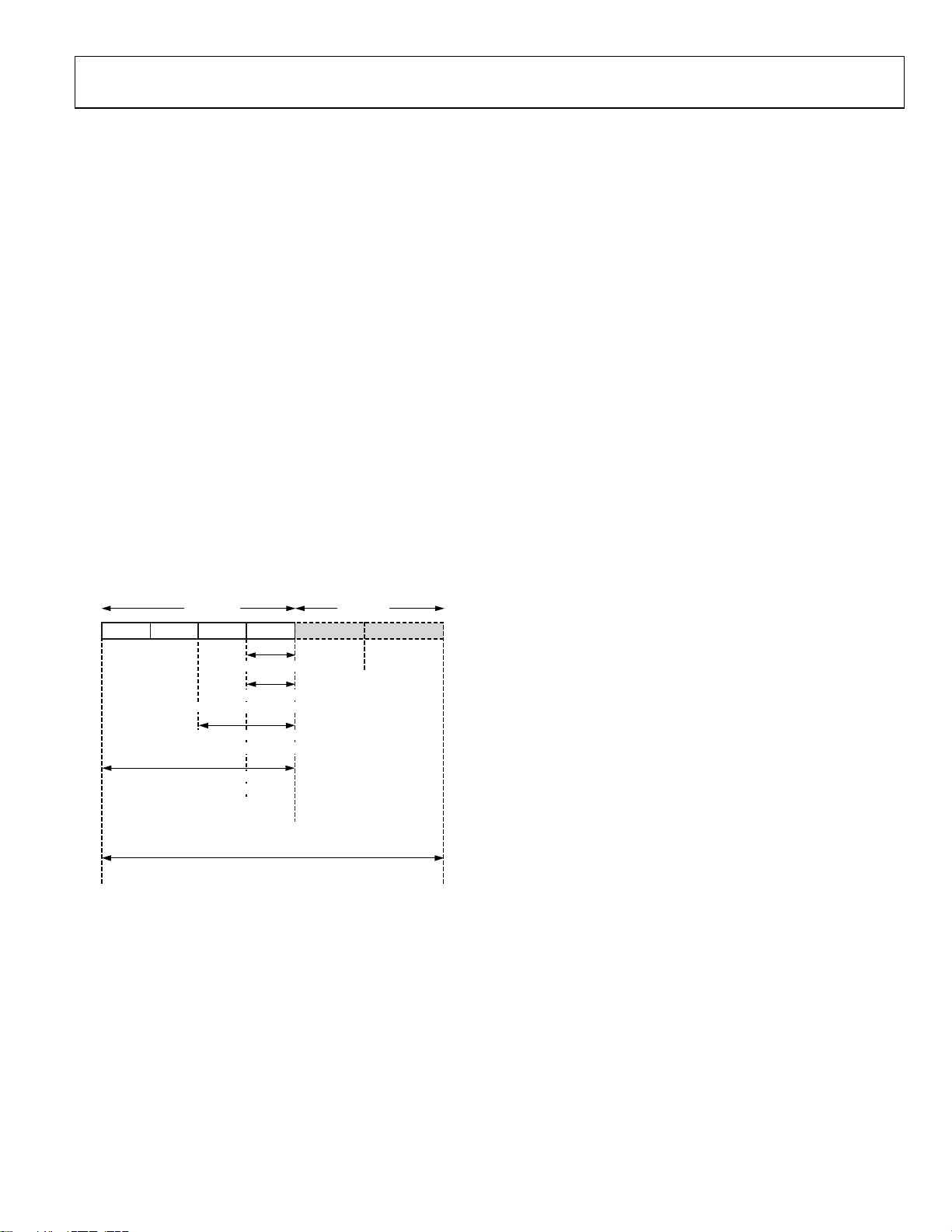
100 MHz. Figure 6 shows the alignment of various accesses to
external memory.
DATA 47
–
16 DATA 15–0
47 40 39 32 31 24 23 16 15 8 7
PROM BOOT
8-BIT PACKED DMA DATA
8-BIT PACKED INSTRUCTION EXECUTION
16-BIT PACKED DMA DATA
16-BIT PACKED INSTRUCTION EXECUTION
FLOAT OR FIXED, D31–D0, 32-BIT PACKED
32-BIT PACKED INSTRUCTION
48-BIT INSTRUCTION FETCH
(NO PACKING)
Figure 6. External Data Alignment Options
L1DATA[7:0]
DATA 15
EXTRA DATA LINES DATA[15–0]
ARE ONLY ACCESSIBLE IF
LINK PORTS ARE DISABLED.
ENABLE THESE ADDITIONAL
DATA LINES BY SELECTING
IPACK[1:0] = 01 IN SYSCON
–
8
L0DATA[7:0]
DATA7–0
The external port supports asynchronous, synchronous, and
synchronous burst access. Synchronous burst SRAM can be
interfaced gluelessly. The SHARC Mel-100 can also interface
gluelessly to SDRAM. Addressing of an external memory device
is facilitated by on-chip decoding of high-order address lines to
generate memory bank select signals. The SHARC Mel-100
provides programmable memory wait states and external
memory acknowledge controls to enable interfacing to memory
and peripherals with variable access, hold, and disable time
requirements.
0
SDRAM Interface
The SDRAM interface enables the SHARC Mel-100 to transfer
data to and from synchronous DRAM (SDRAM) at the core
clock frequency or one-half the core clock frequency. The
synchronous approach, coupled with the core clock frequency,
supports data transfer at a high throughput—up to
400 Mbytes/s for 32-bit transfers and 600 Mbytes/s for 48-bit
transfers. The SDRAM interface provides a glueless interface
with standard SDRAMs (16 Mbit, 64 Mbit, 128 Mbit, and
256 Mbit) and includes options to support additional buffers
between the SHARC Mel-100 and SDRAM. The SDRAM
interface is extremely flexible and provides capability for
connecting SDRAMs to any one of the SHARC Mel-100
processor’s four external memory banks, with up to all four
banks mapped to SDRAM. Systems with several SDRAM
devices connected in parallel may require buffering to meet
overall system timing requirements. The SHARC Mel-100
supports pipelining of the address and control signals to enable
such buffering between itself and multiple SDRAM devices.
Target Board JTAG Emulator Connector
Analog Devices’ DSP Tools product line of JTAG emulators uses
the IEEE 1149.1 JTAG test access port of the SHARC Mel-100
processor to monitor and control the target board processor
during emulation. Analog Devices’ DSP Tools product line of
JTAG emulators provides emulation at full processor speed,
enabling inspection and modification of memory, registers, and
processor stacks. The processor’s JTAG interface ensures that
the emulator will not affect target system loading or timing. For
complete information on Analog Devices’ DSP Tools product
line of JTAG emulator operation, see the appropriate Emulator
Hardware User's Guide. For detailed information on the
interfacing of Analog Devices’ JTAG emulators with Analog
Devices’ DSP products with JTAG emulation ports, please refer
to the Engineer-to-Engineer Note EE-68, Analog Devices JTAG
Emulation Technical Reference. Both of these documents can be
found on the Analog Devices website at:
http://www.analog.com/dsp/tech_docs.html
DMA Controller
The SHARC Mel-100 processor’s on-chip DMA controller
enables zero-overhead data transfers without processor
intervention. The DMA controller operates independently and
invisibly to the processor core, enabling DMA operations to
occur while the core is simultaneously executing its program
instructions. DMA transfers can occur between the SHARC
Mel-100 processor’s internal memory and external memory,
external peripherals, or a host processor. DMA transfers can
also occur between the SHARC Mel-100 processor’s internal
memory and its serial ports, link ports, or the SPI (serial
peripheral interface) compatible port. External bus packing and
unpacking of 16-, 32-, 48-, or 64-bit words in internal memory
is performed during DMA transfers from either 8-, 16-, or 32bit wide external memory. Fourteen channels of DMA are
Rev. 0 | Page 9 of 28
Page 10

ADSST-SHARC-Mel-100
available on the SHARC Mel-100; two are shared between the
SPI interface and the link ports, eight via the serial ports, and
four via the processor’s external port (for either host processor,
other SHARC Mel-100’s memory or I/O transfers). Programs
can be downloaded to the SHARC Mel-100 using DMA
transfers. Asynchronous off-chip peripherals can control two
DMA channels using DMA request/grant lines (
1–2). Other DMA features include interrupt generation
DMAG
upon completion of DMA transfers, and DMA chaining for
automatic linked DMA transfers.
Multiprocessing
The SHARC Mel-100 offers powerful features tailored to
multiprocessing DSP systems. The external port and link ports
provide integrated glueless multiprocessing support. The
external port supports a unified address space (see Figure 5)
that enables direct interprocessor accesses of each SHARC Mel100 processor’s internal memory-mapped (I/O processor)
registers. All other internal memory can be indirectly accessed
via DMA transfers initiated through the programming of the
IOP DMA parameter and control registers. Distributed bus
arbitration logic is included on-chip for simple, glueless
connection of systems containing up to six SHARC Mel-100
processors and a host processor. Master processor changeover
incurs only one cycle of overhead. Bus arbitration is selectable
as either fixed or rotating priority. Bus lock enables indivisible
read-modify-write sequences for semaphores. A vector
interrupt is provided for interprocessor commands. The
maximum throughput for interprocessor data transfers is
400 Mbytes/s over the external port. Two link ports provide a
second method of multiprocessing communications. Each link
port can support communications to another SHARC Mel-100.
The SHARC Mel-100 running at 100 MHz has a maximum
throughput for interprocessor communications over the links of
200 Mbytes/s. The link ports and cluster multiprocessing can be
used concurrently or independently.
Link Ports
The SHARC Mel-100 features two 8-bit link ports that provide
additional I/O capabilities. With the capability of running at
100 MHz, each link port can support 100 Mbytes/s. Link port
I/O is especially useful for point-to-point interprocessor
communication in multiprocessing systems. The link ports can
operate independently and simultaneously, with a maximum
data throughput of 200 Mbytes/s. Link port data is packed into
48- or 32-bit words and can be directly read by the core
processor, or DMA-transferred to on-chip memory. Each link
port has its own double-buffered input and output registers.
Clock/acknowledge handshaking controls link port transfers.
Transfers are programmable as either transmit or receive.
Serial Ports
The SHARC Mel-100 features four synchronous serial ports
that provide an inexpensive interface to a wide variety of digital
and mixed-signal peripheral devices. Each serial port is made
DMAR
1–2,
up of two data lines, a clock, and frame sync. The data lines can
be programmed to either transmit or receive.
The serial ports operate at up to half the clock rate of the core,
providing each with a maximum data rate of 50 Mbps. The
serial data pins are programmable as either a transmitter or
receiver, providing greater flexibility for serial communications.
Serial port data can be automatically transferred to and from
on-chip memory via a dedicated DMA. Each of the serial ports
features a Time Division Multiplex (TDM) multichannel mode;
two serial ports are TDM transmitters and two serial ports are
TDM receivers (SPORT0 RX paired with SPORT2 TX, SPORT1
RX paired with SPORT3 TX). Each of the serial ports also
2
supports the I
S protocol (an industry-standard interface
commonly used by audio codecs, ADCs, and DACs), with two
2
data pins, enabling four I
devices) per serial port, up to a maximum of 16 I
S channels (using two I2S stereo
2
S channels.
The serial ports enable little-endian or big-endian transmission
formats and word lengths selectable from three bits to 32 bits.
2
S mode, data-word lengths are selectable between eight
For I
bits and 32 bits. Serial ports offer selectable synchronization and
transmit modes as well as optional µ-law or A-law companding.
Serial port clocks and frame syncs can be internally or
externally generated.
Serial Peripheral (Compatible) Interface
Serial Peripheral Interface (SPI) is an industry-standard
synchronous serial link, enabling the SHARC Mel-100 SPI
compatible port to communicate with other SPI compatible
devices. SPI is a 4-wire interface consisting of two data pins, one
device select pin, and one clock pin. It is a full-duplex
synchronous serial interface, supporting both master and slave
modes. The SPI port can operate in a multimaster environment
by interfacing with up to four other SPI compatible devices,
acting as either a master or slave device. The SHARC Mel-100
SPI compatible peripheral implementation also features
programmable baud rate and clock phase/polarities. The
SHARC Mel-100 SPI compatible port uses open-drain drivers
to support a multimaster configuration and to avoid data
contention.
Host Processor Interface
The SHARC Mel-100 host interface enables easy connection to
standard 8-bit, 16-bit, or 32-bit microprocessor buses with little
additional hardware required. The host interface is accessed
through the SHARC Mel-100’s external port. Four channels of
DMA are available for the host interface; code and data
transfers are accomplished with low software overhead. The
host processor requests the SHARC Mel-100’s external bus with
the host bus request (
), host bus grant (
HBR
HBG
), and ready
(REDY) signals. The host can directly read and write the
internal IOP registers of the SHARC Mel-100, and can access
the DMA channel setup and message registers. DMA setup via a
host would enable it to access any internal memory address via
Rev. 0 | Page 10 of 28
Page 11

ADSST-SHARC-Mel-100
V
Ω
DMA transfers. Vector interrupt support provides efficient
execution of host commands.
General-Purpose I/O Ports
The SHARC Mel-100 also contains 12 programmable, generalpurpose I/O pins that can function as either inputs or outputs.
As outputs, these pins can signal peripheral devices; as inputs,
these pins can provide the test for conditional branching.
Program Booting
The internal memory of the SHARC Mel-100 can be booted at
system power-up from either an 8-bit EPROM, a host processor,
the SPI interface, or through one of the link ports. Selection of
the boot source is controlled by the Boot Memory Select (
BMS
EBOOT (EPROM Boot), and Link/Host Boot (LBOOT) pins.
8-, 16-, or 32-bit host processors can also be used for booting.
Phased-Locked Loop and Crystal Double Enable
The SHARC Mel-100 uses an on-chip phase-locked loop (PLL)
to generate the internal clock for the core. The CLK_CFG[1:0]
pins are used to select ratios of 2:1, 3:1, and 4:1. In addition to
the PLL ratios, the
CLKDBL
ratio options. The (1×/2× CLKIN) rate set by the
pin can be used for more clock
CLKDBL
pin
determines the rate of the PLL input clock and the rate at which
the synchronous external port operates. With the combination
of CLK_CFG[1:0] and
CLKDBL
, ratios of 2:1, 3:1, 4:1, 6:1, and
8:1 between the core and CLKIN are supported. See Figure 13.
Power Supplies
The SHARC Mel-100 has separate power supply connections
for the internal (V
/AGND) power supplies. The internal and analog supplies
(AV
DD
), external (V
DDINT
), and analog
DDEXT
must meet the 1.8 V requirement. The external supply must
meet the 3.3 V requirement. All external supply pins must be
connected to the same supply.
Note that the analog supply (AV
) powers the SHARC Mel-100
DD
processor’s clock generator PLL. To produce a stable clock,
provide an external circuit to filter the power input to the AV
DD
pin. Place the filter as close as possible to the pin. For an
example circuit, see Figure 7. To prevent noise coupling, use a
wide trace for the analog ground (AGND) signal and install a
decoupling capacitor as close as possible to the pin.
DDINT
10
0.1µF
Figure 7. Analog Power (AV
AGND
) Filter Circuit
DD
0.01µF
AV
DD
3
2
1
ADSP-21161 #4CLOCK
ADSP-21161 #3
CLKIN
DATA47
RESET
ID2–0
ADSP-21161 #2
CLKIN
DATA47
RESET
ID2–0
ADSP-21161 #1
CLKIN
DATA47
RESET
ID2
–
0
CONTROL
SDCLK[1
ADDR23–0
–
CONTROL
ADDR23
–
CONTROL
BMS
ADDR23
–
WR
ACK
MS3
SBTS
HBR
HBG
REDY
BR6
BR1
RAS
CAS
DQM
SDWE
SDCKE
SDA10
ADDRESS
CONTROL
DATA
16
–
0
16
ADDR
DATA
CS
–
0
16
RD
–
0
CS
–
2
CONTROL
–
0]
ADDR
DATA
OE
WE
ACK
CS
ADDR
DATA
ADDRESS
DATA
RAS
CAS
DQM
WE
CLK
CKE
A10
CS
ADDR
DATA
BOOT
EPROM
(OPTIONAL)
GLOBAL
MEMORY
AND
PERIPHERALS
(OPTIONAL)
HOST
PROCESSOR
INTERFACE
(OPTIONAL)
SDRAM
(OPTIONAL)
RESET
),
Figure 8. Shared Memory Multiprocessing System
Rev. 0 | Page 11 of 28
Page 12

ADSST-SHARC-Mel-100
W
PIN FUNCTION DESCRIPTIONS
The SHARC Mel-100 pin definitions can be found in Table 2
beginning on page 13. Inputs identified as synchronous (S)
must meet timing requirements with respect to CLKIN (or with
respect to TCK for TMS, TDI). Inputs identified as
asynchronous (A) can be asserted asynchronously to CLKIN (or
to TCK for
). Tie or pull unused inputs to V
TRST
except for the following:
• ADDR23–0, DATA47–0, BRST, CLKOUT. (Note that
these pins have a logic level hold circuit enabled on the
SHARC Mel-100 DSP with ID2–0 = 00x.)
, ACK, RD, WR,
•
PA
DMARx, DMAGx
, (ID2–0 = 00x).
(Note that these pins have a pull-up enabled on the
SHARC Mel-100 DSP with ID2–0 = 00x.)
• LxCLK, LxACK, LxDAT7–0 (LxPDRDE = 0). (Note: See
Link Port Buffer Control Register Bit definitions in the
SHARC Mel-100 DSP Hardware Reference.)
• DxA, DxB, SCLKx, SPICLK, MISO, MOSI,
TMS,
Figure 9. JTAG Target Board Connector for JTAG Equipped
, TDI. (Note that these pins have a pull-up.)
TRST
GND
KEY (NO PIN)
BTMS
BTCK
BTRST
BTDI
GND
12
34
56
78
910
11 12
13 14
TOP VIEW
EMU
GND
TMS
TCK
TRST
TDI
TDO
Analog Devices DSP (Jumpers in Place)
12
GND
KEY (NO PIN)
BTMS
BTCK
BTRST
BTDI
34
56
78
910
9
11 12
EMU
GND
TMS
TCK
TRST
TDI
DDEXT
EMU
or GND,
,
0.64"
0.88"
0.24"
Figure 11. JTAG Pod Connector Dimensions
0.10"
0.15"
Figure 12. JTAG Pod Connector Keep-Out Area
The following symbols appear in the Type column of Table 2:
A Asynchronous,
G Ground,
I Input,
O Output,
P Power Supply,
S Synchronous,
(A/D) Active Drive,
(O/D) Open Drain,
T
Three-State (when SBTS
is asserted or when the
SHARC Mel-100 is a bus slave).
Unlike previous SHARC processors, the SHARC Mel-100
contains internal series resistance equivalent to 50 Ω on all
input/output drivers except the CLKIN and XTAL pins.
Therefore, for traces longer than six inches, external series
resistors on control, data, clock, or frame sync pins are not
required to dampen reflections from transmission line effects
for point-to-point connections. However, for more complex
networks such as star configurations, series termination is still
recommended.
GND
13 14
TOP VIE
TDO
Figure 10. JTAG Target Board Connector with No Local Boundary Scan
Rev. 0 | Page 12 of 28
Page 13

SHARC® Mel-100
Table 2. Pin Function Description
Mnemonic Type Function
ACK I/O/S
ADDR23–0 I/O/T
AGND G
AV
DD
BMS
BMSTR O
BR6–1
BRST I/O/T
CAS
CLK_CFG1–0 I
P
I/O/T
I/O/S
I/O/T
Memory Acknowledge. External devices can deassert ACK (low) to add wait states to an external memory
access. ACK is used by I/O devices, memory controllers, or other peripherals to hold off completion of an
external memory access. The SHARC Mel-100 deasserts ACK as an output to add wait states to a synchronous
access of its IOP registers. ACK has a 20 kΩ internal pull-up resistor that is enabled during reset or on DSPs
with ID2–0 = 00x.
External Bus Address. The SHARC Mel-100 outputs addresses for external memory and peripherals on these
pins. In a multiprocessor system, the bus master outputs addresses for read/writes of the IOP registers of
other SHARC Mel-100 processors, while all other internal memory resources can be accessed indirectly via
DMA control (that is, accessing IOP DMA parameter registers). The SHARC Mel-100 inputs addresses when a
host processor or multiprocessing bus master is reading or writing its IOP registers. A keeper latch on the
DSP’s ADDR23–0 pins maintains the input at the level to which it was last driven. This latch is only enabled on
the SHARC Mel-100 with ID2–0 = 00x.
Analog Power Supply Return.
Analog Power Supply. Nominally +1.8 V dc and supplies the DSP’s internal PLL (clock generator). This pin
has the same specifications as V
section.
Boot Memory Select. Serves as an output or input as selected with the EBOOT and LBOOT pins; see Table 3
on page 17. This input is a system configuration selection that should be hardwired. For Host and EPROM
boot, DMA Channel 10 (EPB0) is used. For Link boot and SPI boot, DMA Channel 8 is used. Three-state only in
EPROM boot mode (when BMS
Bus Master Output. In a multiprocessor system, indicates whether the SHARC Mel-100 is current bus master
of the shared external bus. The SHARC Mel-100 drives BMSTR high only while it is the bus master. In a singleprocessor system (ID = 000), the processor drives this pin high.
Multiprocessing Bus Requests. Used by multiprocessing SHARC Mel-100 processors to arbitrate for bus
mastership. A SHARC Mel-100 only drives its own BR
monitors all others. In a multiprocessor system with less than six SHARC Mel-100 processors, the unused BR
pins should be pulled high; the processor’s own BR
output.
Sequential Burst Access. BRST is asserted by SHARC Mel-100 to indicate that data associated with
consecutive addresses is being read or written. A slave device samples the initial address and increments an
internal address counter after each transfer. The incremented address is not pipelined on the bus. A master
SHARC Mel-100 in a multiprocessor environment can read slave external port buffers (EPBx) using the burst
protocol. BRST is asserted after the initial access of a burst transfer. It is asserted for every cycle after that,
except for the last data request cycle (denoted by RD
the DSP’s BRST pin maintains the input at the level to which it was last driven. This latch is only enabled on
the SHARC Mel-100 with ID2–0 = 00x.
SDRAM Column Access Strobe. In conjunction with RAS
defines the operation for the SDRAM to perform.
Core/CLKIN Ratio Control. SHARC Mel-100 core clock (instruction cycle) rate is equal to n × PLLICLK where n
is user selectable to 2, 3, or 4, using the CLK_CFG1–0 inputs. These pins can also be used in combination with
the CLKDBL
table in the CLKDBL
pin to generate additional core clock rates of 6 × CLKIN and 8 × CLKIN (see the Clock Rate Ratios
is an output).
description).
Audio Processor
ADSST-SHARC-Mel-100
, except that added filtering circuitry is required. See the Power Supplies
DDINT
x line (corresponding to the value of its ID2–0 inputs) and
x line must not be pulled high or low because it is an
or WR asserted and BRST negated). A keeper latch on
, MSx, SDWE, SDCLKx, and sometimes SDA10,
x
Rev. 0
Information furnished by Analog Devices is believed to be accurate and reliable.
However, no responsibility is assumed by Analog Devices for its use, nor for any
infringements of patents or other rights of third parties that may result from its use.
Specifications subject to change without notice. No license is granted by implication
or otherwise under any patent or patent rights of Analog Devices. Trademarks and
registered trademarks are the property of their respective owners.
One Technology Way, P.O. Box 9106, Norwood, MA 02062-9106, U.S.A.
Tel: 781.329.4700 www.analog.com
Fax: 781.326.8703 © 2003 Analog Devices, Inc. All rights reserved.
Page 14

ADSST-SHARC-Mel-100
CLKDBL
CLKIN I
CLKOUT O/T
CS
DATA47–16 I/O/T
DMAG1
DMAG2
I
I/A
O/T
O/T
Crystal Double Mode Enable. This pin is used to enable the 2× clock double circuitry, where CLKOUT can be
configured as either 1× or 2× the rate of CLKIN. This CLKIN double circuit is primarily intended to be used for
an external crystal in conjunction with the internal clock generator and the XTAL pin. The internal clock
generator, when used in conjunction with the XTAL pin and an external crystal, is designed to support up to a
maximum of 25 MHz external crystal frequency. CLKDBL
input into the PLL. The 2× clock mode is enabled (during RESET
connected to V
100 MHz core clock rates and a 50 MHz CLKOUT operation when CLK_CFG1= 0, CLK_CFG1= 0, and
CLKDBL
possible clock rate ratio options (up to 100 MHz) for either CLKIN (external clock oscillator) or XTAL (crystal
input) are as follows:
Clock Rate Ratios
CLKDBL
1 0 0 2:1 1×
1 0 1 3:1 1×
0 1 0 4:1 1×
0 0 0 4:1 2×
0 0 1 6:1 2×
0 1 0 8:1 2×
An 8:1 ratio enables the use of a 12.5 MHz crystal to generate a 100 MHz core (instruction clock) rate and a
25 MHz CLKOUT (external port) clock rate. See Figure 13.
Note that when using an external crystal, the maximum crystal frequency cannot exceed 25 MHz. For all
other external clock sources, the maximum CLKIN frequency is 50 MHz.
Local Clock In. Used in conjunction with XTAL. CLKIN is the SHARC Mel-100’s clock input. It configures the
SHARC Mel-100 to use either its internal clock generator or an external clock source. Connecting the
necessary components to CLKIN and XTAL enables the internal clock generator. Connecting the external
clock to CLKIN while leaving XTAL unconnected configures the SHARC Mel-100 to use the external clock
source such as an external clock oscillator.The SHARC Mel-100 external port cycles at the frequency of CLKIN.
The instruction cycle rate is a multiple of the CLKIN frequency; it is programmable at power-up via the
CLK_CFG1–0 pins. CLKIN may not be halted, changed, or operated below the specified frequency.
Local Clock Out. CLKOUT is 1× or 2× and is driven at either 1× or 2× the frequency of CLKIN frequency by the
current bus master. The frequency is determined by the CLKDBL
SHARC Mel-100 is not the bus master or when the host controls the bus (HBG
DSP’s CLKOUT pin maintains the output at the level it was last driven. This latch is only enabled on the SHARC
Mel-100 with ID2–0 = 00x.
If CLKDBL
If CLKDBL
Note that CLKOUT is controlled only by the CLKDBL
Do not use CLKOUT in multiprocessing systems; use CLKIN instead.
Chip Select. Asserted by host processor to select the SHARC Mel-100.
External Bus Data. The SHARC Mel-100 inputs and outputs data and instructions on these pins. Pull-up
resistors on unused data pins are not necessary. A keeper latch on the DSP’s DATA47–16 pins maintains the
input at the level to which it was last driven. This latch is only enabled on the SHARC Mel-100 with
ID2–0 = 00x.
Note that DATA[15:8] pins (multiplexed with L1DATA[7:0]) can also be used to extend the data bus if the link
ports are disabled and will not be used. In addition, DATA[7:0] pins (multiplexed with L0DATA[7:0]) can also
be used to extend the data bus if the link ports are not used. This enables execution of 48-bit instructions
from external SBSRAM (system clock speed-external port), SRAM (system clock speed-external port), and
SDRAM (core clock or one-half the core clock speed). The IPACKx instruction packing mode bits in SYSCON
should be set correctly (IPACK1–0 = 0x1) to enable this full instruction width/no-packing mode of operation.
DMA Grant 1 (DMA Channel 11). Asserted by SHARC Mel-100 to indicate that the requested DMA starts on
the next cycle. Driven by bus master only. DMAG1
DSPs with ID2–0 = 00x.
DMA Grant 2 (DMA Channel 12). Asserted by the SHARC Mel-100 to indicate that the requested DMA starts
on the next cycle. Driven by the bus master only. DMAG2
for DSPs with ID2–0 = 00x.
can be used in XTAL mode to generate a 50 MHz
low) by tying CLKDBL to GND, otherwise it is
for 1× clock mode. For example, this enables the use of a 25 MHz crystal to enable
DDEXT
= 0. This pin can also be used to generate different clock rate ratios for external clock oscillators. The
CLK_CFG1 CLK_CFG0 Core:CLKIN CLKIN:CLKOUT
pin. This output is three-stated when the
asserted). A keeper latch on the
enabled, CLKOUT = 2 × CLKIN
disabled, CLKOUT = 1 × CLKIN
pin and operates at either 1 × CLKIN or 2 × CLKIN.
has a 20 kΩ internal pull-up resistor that is enabled for
has a 20 kΩ internal pull-up resistor that is enabled
Rev. 0 | Page 14 of 28
Page 15

ADSST-SHARC-Mel-100
DMAR1
DMAR2
DQM O/T
DxA I/O
DxB I/O
EBOOT I
EMU
FLAG11–0 I/O/A
FSx I/O
GND G
HBG
HBR
ID2–0 I
IRQ2–0
LBOOT I
LxACK I/O
LxCLK I/O
LxDAT7–0
[DATA15–0]
I/A
I/A
(O/D)
I/O
I/A
I/A
I/O
[I/O/T]
DMA Request 1 (DMA Channel 11). Asserted by external port devices to request DMA services. DMAR1
20 kΩ internal pull-up resistor that is enabled for DSPs with ID2–0 = 00x.
DMA Request 2 (DMA Channel 12). Asserted by external port devices to request DMA services. DMAR2
20 kΩ internal pull-up resistor that is enabled for DSPs with ID2–0 = 00x.
SDRAM Data Mask. In write mode, DQM has a latency of zero and is used during a precharge command and
during SDRAM power-up initialization.
Data Transmit or Receive Channel A (Serial Ports 0, 1, 2, 3). Each DxA pin has an internal pull-up resistor.
Bidirectional data pin. This signal can be configured as an output to transmit serial data, or as an input to
receive serial data.
Data Transmit or Receive Channel B (Serial Ports 0, 1, 2, 3). Each DxB pin has an internal pull-up resistor.
Bidirectional data pin. This signal can be configured as an output to transmit serial data, or as an input to
receive serial data.
EPROM Boot Select. For a description of how this pin operates, see Table 3 on page 17. This signal is a
system configuration selection that should be hardwired.
Emulation Status. Must be connected to the SHARC Mel-100 Analog Devices’ DSP Tools product line of JTAG
emulators target board connector only. EMU
Flag Pins. Each pin is configured via control bits as either an input or output. As an input, it can be tested as a
condition. As an output, it can be used to signal external peripherals.
Transmit or Receive Frame Sync (Serial Ports 0, 1, 2, 3). The frame sync pulse initiates shifting of serial data.
This signal is either generated internally or externally. It can be active high or low or an early or late frame
sync, in reference to the shifting of serial data.
Power Supply Return (26 pins).
Host Bus Grant. Acknowledges an HBR
the external bus. HBG
system, HBG
and before HBG
pulled up with a 20 kΩ to 50 kΩ external resistor.
Host Bus Request. Must be asserted by a host processor to request control of the SHARC Mel-100 processor’s
external bus. When HBR
relinquish the bus and assert HBG
and strobe lines in a high impedance state. HBR
multiprocessing system.
Multiprocessing ID. Determines which multiprocessing bus request (BR
ID = 001 corresponds to BR1
processor systems. These lines are a system configuration selection that should be hardwired or only
changed at reset.
Interrupt Request Lines. These pins are sampled on the rising edge of CLKIN and may be either edge-
triggered or level-sensitive.
Link Boot. For a description of how this pin operates, see Table 3 on page 17. This signal is a system
configuration selection that should be hardwired.
Link Port Acknowledge (Link Ports 0–1). Each LxACK pin has an internal pull-down 50 kΩ resistor that is
enabled or disabled by the LxPDRDE bit of the LCTL register.
Link Port Clock (Link Ports 0–1). Each LxCLK pin has an internal pull-down 50 kΩ resistor that is enabled or
disabled by the LxPDRDE bit of the LCTL register.
Link Port Data (Link Ports 0–1).
For silicon revisions 1.2 and higher, each LxDAT pin has a keeper latch that is enabled when used as a data
pin, or a 20 kΩ internal pull-down resistor that is enabled or disabled by the LxPDRDE bit of the LCTL register.
For silicon revisions 0.3, 1.0, and 1.1, each LxDAT pin has a 50 kΩ internal pull-down resistor that is enabled or
disabled by the LxPDRDE bit of the LCTL register.
Note that L1DATA[7:0] are multiplexed with the DATA[15:8] pins; L0DATA[7:0] are multiplexed with the
DATA[7:0] pins. If link ports are disabled and are not be used, these pins can be used as additional data lines
for executing instructions at up to the full clock rate from external memory. See DATA47–16 for more
information.
is output by the SHARC Mel-100 bus master and is monitored by all others. After HBR is asserted,
is asserted (held low) by the SHARC Mel-100 until HBR is released. In a multiprocessing
is given, HBG will float for 1 tCK (1 CLKIN cycle). To avoid erroneous grants, HBG should be
is asserted in a multiprocessing system, the SHARC Mel-100 that is bus master will
. To relinquish the bus, the SHARC Mel-100 places the address, data, select,
, ID = 010 corresponds to BR2, and so on. Use ID = 000 or ID = 001 in single-
has an internal pull-up resistor.
bus request, indicating that the host processor may take control of
has priority over all SHARC Mel-100 bus requests (BR6–1) in a
6–1) is used by the SHARC Mel-100.
has a
has a
Rev. 0 | Page 15 of 28
Page 16

ADSST-SHARC-Mel-100
MISO I/O (O/D)
MOSI I/O (O/D)
MS3–0
NC
PA
RAS
RD
REDY O (O/D)
RESET
RPBA I/S
RSTOUT
SBTS
SCLKx I/O
SDA10 O/T
SDCLK0 I/O/S/T
SDCLK1 O/S/T
SDCKE I/O/T
SDWE
I/O/T
I/O/T
I/O/T
I/O/T
I/A
O
I/S
I/O/T
SPI Master In Slave Out. If the SHARC Mel-100 is configured as a master, the MISO pin becomes a data
receive (input) pin. If the SHARC Mel-100 is configured as a slave, the MISO pin becomes a data transmit
(output) pin. In a SHARC Mel-100 SPI interconnection, the data is shifted out from the MISO output pin of the
slave and shifted into the MISO input pin of the master. MISO has an internal pull-up resistor. MISO can be
configured as O/D by setting the OPD bit in the SPICTL register.
Note that only one slave is enabled to transmit data at any given time.
SPI Master Out Slave. If the SHARC Mel-100 is configured as a master, the MOSI pin becomes a data transmit
(output) pin. If the SHARC Mel-100 is configured as a slave, the MOSI pin becomes a data receive (input) pin.
In aSHARC Mel-100 SPI interconnection, the data is shifted out from the MOSI output pin of the master and
shifted into the MOSI input(s) of the slave(s). MOSI has an internal pull-up resistor.
Memory Select Lines. These outputs are asserted (low) as chip selects for the corresponding banks of
external memory. Memory bank sizes are fixed to 16 Mwords for non-SDRAM and 64 Mwords for SDRAM. The
MS
3–0 outputs are decoded memory address lines. In asynchronous access mode, the MS3–0 outputs
transition with the other address outputs. In synchronous access modes, the MS
other address lines; however, they de-assert after the first CLKIN cycle in which ACK is sampled asserted. In a
multiprocessor systems, the MS
zeros and 26 and 27 are decoded into MS
Do Not Connect. Reserved pins that must be left open and unconnected (5 pins).
Priority Access. Asserting its PA
transfers and gain access to the external bus. PA
If access priority is not required in a system, PA
resistor that is enabled for DSPs with ID2–0 = 00x.
SDRAM Row Access Strobe. In conjunction with CAS
defines the operation for the SDRAM to perform.
Memory Read Strobe. RD
from the IOP registers of other SHARC Mel-100 processors. External devices, including other SHARC Mel-100
processors, must assert RD
multiprocessing system, RD
enabled for DSPs with ID2–0 = 00x.
Host Bus Acknowledge. The SHARC Mel-100 deasserts REDY (low) to add wait states to a host access of its
IOP registers when CS
Processor Reset. Resets the SHARC Mel-100 to a known state and begins execution at the program memory
location specified by the hardware reset vector address. The RESET
Rotating Priority Bus Arbitration Select. When RPBA is high, rotating priority for multiprocessor bus
arbitration is selected. When RPBA is low, fixed priority is selected. This signal is a system configuration
selection that must be set to the same value on every SHARC Mel-100. If the value of RPBA is changed during
system operation, it must be changed in the same CLKIN cycle on every SHARC Mel-100.
Reset Out. When RSTOUT
4096 cycles after RESET
silicon revision 1.2.)
Suspend Bus and Three-State. External devices can assert SBTS
data, selects, and strobes in a high impedance state for the following cycle. If the SHARC Mel-100 attempts to
access external memory while SBTS
completed until SBTS
deadlock.
Transmit/Receive Serial Clock (Serial Ports 0, 1, 2, 3). Each SCLK pin has an internal pull-up resistor. This
signal can be either internally or externally generated.
SDRAM A10 Pin. Enables applications to refresh an SDRAM in parallel with a non-SDRAM accesses or host
accesses.
SDRAM Clock Output 0. Clock for SDRAM devices.
SDRAM Clock Output 1. Additional clock for SDRAM devices. For systems with multiple SDRAM devices, this
pin handles the increased clock load requirements, eliminating the need for off-chip clock buffers. Either
SDCLK1 or both SDCLKx pins can be three-stated.
SDRAM Clock Enable. Enables and disables the CLK signal. For details, see the data sheet supplied with the
SDRAM device.
SDRAM Write Enable. In conjunction with CAS
the operation for the SDRAM to perform.
3–0 outputs assert with the
x signals are tracked by slave SHARCs. The internal addresses 24 and 26 are
3–0.
pin enables a SHARC Mel-100 bus slave to interrupt background DMA
is connected to all SHARC Mel-100 processors in the system.
should be left unconnected. PA has a 20 kΩ internal pull-up
, MSx, SDWE, SDCLKx, and sometimes SDA10, this pin
is asserted whenever the SHARC Mel-100 reads a word from external memory or
for reading a word of the SHARC Mel-100 IOP register memory. In a
is driven by the bus master. RD has a 20 kΩ internal pull-up resistor that is
and HBR inputs are asserted.
input must be asserted (low) at power-up.
is asserted (low), this pin indicates that the core blocks are in reset. It is deasserted
is deasserted indicating that the PLL is stable and locked. (RSTOUT exists only for
(low) to place the external bus address,
is asserted, the processor will halt and the memory access will not be
is deasserted. SBTS should only be used to recover from host processor/SHARC Mel-100
, RAS, MSx, SDCLKx, and sometimes SDA10, this pin defines
Rev. 0 | Page 16 of 28
Page 17

ADSST-SHARC-Mel-100
SPICLK I/O
SPIDS
I
TCK I
TDI I/S
TDO O
TIMEXP O
TMS I/S
TRST
V
DDINT
V
DDEXT
WR
I/A
P
P
I/O/T
XTAL O
Serial Peripheral Interface Clock Signal. Driven by the master, this signal controls the rate at which data is
transferred. The master may transmit data at a variety of baud rates.
SPICLK cycles once for each bit transmitted. SPICLK is a gated clock that is active during data transfers, only
for the length of the transferred word. Slave devices ignore the serial clock if the slave select input is driven
inactive (high). SPICLK is used to shift out and shift in the data driven on the MISO and MOSI lines. The data is
always shifted out on one clock edge of the clock and sampled on the opposite edge of the clock. Clock
polarity and clock phase relative to data are programmable into the SPICTL control register and define the
transfer format. SPICLK has an internal pull-up resistor.
Serial Peripheral Interface Slave Device Select. An active low signal used to enable slave devices. This
input signal behaves like a chip select, and is provided by the master device for the slave devices. In
multimaster mode, the SPIDS
signal can be asserted to a master device to signal that an error has occurred
because some other device is also trying to be the master device. If asserted low when the device is in master
mode, it is considered a multimaster error. For a single-master, multiple-slave configuration where FLAG3–0
are used, this pin must be tied or pulled high to V
on the master device. For SHARC Mel-100 to SHARC
DDEXT
Mel-100 SPI interaction, any of the master SHARC Mel-100 processors’ FLAG3–0 pins can be used to drive the
SPIDS
signal on the SHARC Mel-100 SPI slave device.
Test Clock (JTAG). Provides a clock for JTAG boundary scan.
Test Data Input (JTAG). Provides serial data for the boundary scan logic. TDI has a 20 kΩ internal pull-up
resistor.
Test Data Output (JTAG). Serial scan output of the boundary scan path.
Timer Expired. Asserted for four core clock cycles when the timer is enabled.
Test Mode Select (JTAG). Used to control the test state machine. TMS has a 20 kΩ internal pull-up resistor.
Test Reset (JTAG). Resets the test state machine. TRST
low for proper operation of the SHARC Mel-100. TRST
must be asserted (pulsed low) After power-up or held
has a 20 kΩ internal pull-up resistor.
Core Power Supply. Nominally 1.8 V dc and supplies the DSP’s core processor (14 pins).
I/O Power Supply. Nominally 3.3 V dc (13 pins).
Memory Write Low Strobe. WR
IOP registers of other SHARC Mel-100 processors. External devices must assert WR
Mel-100’s IOP registers. In a multiprocessing system, WR
is asserted when the SHARC Mel-100 writes a word to external memory or
for writing to the SHARC
is driven by the bus master. WR has a 20 kΩ internal
pull-up resistor that is enabled for DSPs with ID2–0 = 00x.
Crystal Oscillator Terminal 2. Used in conjunction with CLKIN to enable the SHARC Mel-100’s internal clock
oscillator or to disable it to use an external clock source. See CLKIN.
BOOT MODES
Table 3. Boot Mode Selection
EBOOT LBOOT
1 0 Output
0 0 1 (Input) Host Processor.
0 1 0 (Input) Serial Boot via SPI.
0 1 1 (Input) Link Port.
0 0 0 (Input) No Booting. Processor executes from external memory.
1 1 x (Input) Reserved.
Booting Mode
BMS
EPROM (Connect BMS
Rev. 0 | Page 17 of 28
to EPROM chip select).
Page 18

ADSST-SHARC-Mel-100
SPECIFICATIONS
RECOMMENDED OPERATING CONDITIONS
Table 4.
C Grade K Grade
Parameter Test Conditions Min Max Min Max Unit
V
Internal (Core) Supply Voltage 1.71 1.89 1.71 1.89 V
DDINT
AVDD Analog (PLL) Supply Voltage 1.71 1.89 1.71 1.89 V
V
External (I/O) Supply Voltage 3.13 3.47 3.13 3.47 V
DDEXT
VIH High Level Input Voltage
VIL Low Level Input Voltage2 @ V
T
Case Operating Temperature
CASE
2
Applies to input and bidirectional pins: DATA47–16, ADDR23–0, MS3–0, RD, WR, ACK,
BRST, FSx, DxA, DxB, SCLKx,
RESET
, TRST, TCK, TMS, TDI.
3
See the Thermal Characteristics section on page 23 for information on thermal specifications.
RAS
CAS, SDWE
,
2
3
, SDCLK0, LxDAT7–0, LxCLK, LxACK, SPICLK, MOSI, MISO,
@ V
= max 2.0 V
DDEXT
= min –0.5 0.8 –0.5 0.8 V
DDEXT
–40 +105 0 +85 °C
SBTS
, IRQ2–0, FLAG11–0,
SPIDS
, EBOOT, LBOOT,
+ 0.5 2.0 V
DDEXT
HBG, HBR, CS, DMAR1, DMAR2, BR
BMS
, SDCKE, CLK_CFGx,
+ 0.5 V
DDEXT
6–1, ID2–0, RPBA, PA,
CLKDBL
, CLKIN,
Rev. 0 | Page 18 of 28
Page 19

ADSST-SHARC-Mel-100
ELECTRICAL CHARACTERISTICS
Table 5.
Parameter Test Conditions Min Max Unit
VOH High Level Output Voltage
V
OL
Low Level Output Voltage4 @ V
IIH High Level Input Current
IIL Low Level Input Current6 @ V
I
CLKIN High Level Input Current
IHC
I
CLKIN Low Level Input Current8 @ V
ILC
I
IKH
I
IKL
I
Keeper High Overdrive Current
IKH-OD
I
IKL-OD
I
Low Level Input Current Pull-Up7 @ V
ILPU
I
Three-State Leakage Current
OZH
I
Three-State Leakage Current
OZL
I
Three-State Leakage Current Pull-Up113 @ V
OZLPU1
I
Three-State Leakage Current Pull-Up214 @ V
OZLPU2
I
Three-State Leakage Current Pull-Down1
OZHPD1
I
Three-State Leakage Current Pull-Down2
OZHPD2
I
DD-INPEAK
I
DD-INHIGH
I
DD-INLOW
I
DD-IDLE
Keeper High Load Current
Keeper Low Load Current9 @ V
Keeper Low Overdrive Current
Supply Current (Internal)
Supply Current (Internal)
Supply Current (Internal)
Supply Current (Idle)
AIDD Supply Current (Analog)
CIN Input Capacitance
4
Applies to output and bidirectional pins: DATA47–16, ADDR23–0, MS3–0, RD, WR, ACK, DQM, FLAG11–0,
DxA, DxB, SCLKx,
5
See the Output Drive Currents section on page 21 for typical drive current capabilities.
6
Applies to input pins: DATA47–16, ADDR23–0, MS3–0,
SDCLK0, LxDAT7–0, LxCLK, LxACK, SPICLK, MOSI, MISO,
7
Applies to input pins with 20 kΩ internal pull-ups: RD, WR, ACK,
8
Applies to CLKIN only.
9
Applies to all pins with keeper latches: ADDR23–0, DATA47–0, MS3–0, BRST, CLKOUT.
10
Current required to switch from kept high to low or from kept low to high.
11
Characterized, but not tested.
12
Applies to three-statable pins: DATA47–16, ADDR23–0, MS3–0, CLKOUT, FLAG11–0, REDY,
13
Applies to three-statable pins with 20 kΩ pull-ups: RD, WR,
14
Applies to three-statable pins with 50 kΩ internal pull-ups: DxA, DxB, SCLKx, SPICLK,
15
Applies to three-statable pins with 50 kΩ internal pull-downs: LxDAT7–0 (below Revision1.2), LxCLK, LxACK. Use I
16
Applies to three-statable pins with 20 kΩ internal pull-downs: LxDAT7–0 (Revision 1.2 and higher).
17
The test program used to measure I
power measurements made using typical applications are less than specified. For more information, see the Power Dissipation section on page 21.
18
Current numbers are for V
19
I
is a composite average based on a range of high activity code. See the Power Dissipation section on page 21.
DD-INHIGH
20
I
is a composite average based on a range of low activity code. See the Power Dissipation section on page 21.
DD-INLOW
21
Idle denotes SHARC MEL-100 state during execution of IDLE instruction. See the Power Dissipation section on page 21.
22
Characterized, but not tested.
23
Applies to all signal pins.
24
Guaranteed, but not tested.
RAS
CAS, SDWE
,
DDINT
23, 24
, SDA10, LxDAT7–0, LxCLK, LxACK, SPICLK, MOSI, MISO,
DD-INPEAK
and AVDD supplies combined.
4
6, 7
8
9
, , 10 11
9
9, 10, 11
12, , 13 14
, 12, 13
12
15
16
17, 18
, 19
18
, 20
18
, 21
18
22
SBTS
, IRQ2–0, FLAG11–0,
SPIDS
, EBOOT, LBOOT,
DMAR1, DMAR2, PA
@ V
= min, IOH = –2.0 mA
DDEXT
= min, IOL = 4.0 mA5 0.4 V
DDEXT
@ V
= max, VIN = V
DDEXT
= max, VIN = 0 V 10 µA
DDEXT
@ V
= max, VIN = V
DDEXT
= max, VIN = 0 V 25 µA
DDEXT
@ V
= max, VIN = 2.0 V –250 –100 µA
DDEXT
= max, VIN = 0.8 V 50 200 µA
DDEXT
@ V
= max –300 µA
DDEXT
@ V
= max 300 µA
DDEXT
= max, VIN = 0 V 250 µA
DDEXT
@ V
= max, VIN = V
DDEXT
@ V
= max, VIN = 0 V 10 µA
DDEXT
= max, VIN = 0 V 500 µA
DDEXT
= max, VIN = 0 V 250 µA
DDEXT
@ V
= max, VIN = V
DDEXT
@ V
= max, VIN = V
DDEXT
t
= 10.0 ns, V
CCLK
t
= 10.0 ns, V
CCLK
t
= 10.0 ns, V
CCLK
t
= 10.0 ns, V
CCLK
= max 900 mA
DDINT
= max 650 mA
DDINT
= max 500 mA
DDINT
= max 400 mA
DDINT
@AVDD = max 10 mA
fIN = 1 MHz, T
HBG, HBR, CS, BR
BMS
, SDCKE, CLK_CFGx,
, TRST, TMS, TDI.
= 25°C, VIN = 1.8 V 4.7 pF
CASE
BMS
, SDCLKx, SDCKE,
6–1, ID2–0, RPBA, BRST, FSx, DxA, DxB, SCLKx,
HBG, BMS, BR
DMAG1, DMAG2, PA
.
EMU
, MISO, MOSI.
5
max 10 µA
DDEXT
max 25 µA
DDEXT
max 10 µA
DDEXT
max 250 µA
DDEXT
max 500 µA
DDEXT
HBG
DMAG1, DMAG2, BR
, REDY,
EMU
, XTAL, TDO, CLKOUT, TIMEXP,
2.4 V
6–1, BMSTR, PA, BRST, FSx,
RSTOUT
RAS, CAS, SDWE
CLKDBL
6-1,
RESET
, TCK,
RAS, CAS, SDWE
for Rev. 1.2 and higher.
OZHPD2
, CLKIN.
, DQM, SDCLKx, SDCKE, SDA10, BRST.
.
represents worst-case processor operation and is not sustainable under normal application conditions. Actual internal
,
Rev. 0 | Page 19 of 28
Page 20

ADSST-SHARC-Mel-100
z
ABSOLUTE MAXIMUM RATINGS
Table 6.
Parameter Rating
Internal (Core) Supply Voltage (V
) –0.3 V to +2.2 V
DDINT
Analog (PLL) Supply Voltage (AVDD) –0.3 V to +2.2 V
External (I/O) Supply Voltage (V
Input Voltage –0.5 V to V
Output Voltage Swing –0.5 V to V
) –0.3 V to +4.6 V
DDEXT
DDEXT
DDEXT
+ 0.5 V
+ 0.5 V
Load Capacitance 200 pF
Storage Temperature Range –65°C to +150°C
Stresses greater than those listed above may cause permanent
damage to the device. These are stress ratings only; functional
operation of the device at these or any other conditions greater
than those indicated in the operational sections of this
specification is not implied. Exposure to absolute maximum
rating conditions for extended periods may affect device
reliability.
TIMING SPECIFICATIONS
The SHARC Mel-100 processor’s internal clock switches at
higher frequencies than the system input clock (CLKIN). To
generate the internal clock, the processor uses an internal
phase-locked loop (PLL). This PLL based clocking minimizes
the skew between the system clock (CLKIN) signal and the
processor’s internal clock (the clock source for the external port
logic and I/O pads).
The SHARC Mel-100 processor’s internal clock (a multiple of
CLKIN) provides the clock signal for timing internal memory,
processor core, link ports, serial ports, and external port (as
required for read/write strobes in asynchronous access mode).
During reset, program the ratio between the processor’s internal
clock frequency and external (CLKIN) clock frequency with the
CLK_CFG1–0 and
clock is the clock source for the external port, it behaves as
described on the Clock Rate Ratio chart in
description in Table 2. To determine switching frequencies for
the serial and link ports, divide down the internal clock using
the programmable divider control of each port (DIVx for the
serial ports and LxCLKD for the link ports).
CLKDBL
pins. Even though the internal
CLKDBL
pin
CLKIN
(4.2MH
–50MHz)
XTAL
QUARTZ
CRYSTAL OR
CRYSTAL
OSCILLATOR
EP:
MULTIPROCESSING
HOST
SRAM
SBSRAM
CCLK
(33.3MHz
TO 100MHz)
IO-PROCESSOR
×1/2, ×1 BY SW
LINK PORT:
×1, ×1/2, ×1/3,
×1/4 BY SW
CORE
EP:
SDRAM
CLOCK
DOUBLER
×1, ×2
CLKDBL
PLLICLK
(8.4MHz–50MHz)
RATIOS
×2, ×3, ×4
PLL
CLK_CFG[1:0]
Figure 13. Core Clock and System Relationship to CLKIN
CLKOUT
LCLK[1:0]
SDCLK[1:0]
Rev. 0 | Page 20 of 28
Page 21

ADSST-SHARC-Mel-100
0
C
∆
POWER DISSIPATION
Total power dissipation has two components: one due to
internal circuitry and one due to the switching of external
output drivers. Internal power dissipation depends on the
instruction execution sequence and the data operands involved.
Using the current specifications (I
) from the Electrical Characteristics (Table 5 on page 19),
I
DD-IDLE
DD-INPEAK
, I
the programmer can estimate the SHARC Mel-100 processor’s
internal power supply (V
) input current for a specific
DDINT
application, according to the following formula:
= % Peak × I
I
DDINT
+ % High × I
+ % Low × I
+ % Idle × I
DD-INPEAK
DD-INHIGH
DD-INLOW
DD-IDLE
The external component of total power dissipation is caused by
the switching of output pins. Its magnitude depends on
• The number of output pins that switch during each cycle
(O)
• The maximum frequency at which they can switch (f)
• Their load capacitance (C)
• Their voltage swing (V
)
DD
and is calculated by
= O × C × V
P
EXT
2
× f
DD
The load capacitance should include the processor package
capacitance (C
). The switching frequency includes driving the
IN
load high and then back low. Address and data pins can drive
high and low at a maximum rate of 1/t
while writing to an
CK
SDRAM memory.
Example:
Estimate P
with the following assumptions:
EXT
• A system with one bank of external memory (32 bit)
• Two 1M × 16 SDRAM chips are used, each with a load
of 10 pF (ignoring trace capacitance)
• External data memory writes can occur every cycle at a
rate of 1/t
, with 50% of the pins switching
CK
• The bus cycle time is 50 MHz
• The external SDRAM clock rate is 100 MHz
• SDRAM refresh cycles are ignored
• Addresses are incremental and on the same page
The P
equation is calculated for each class of pins that can
EXT
drive.A typical power consumption can now be calculated for
these conditions by adding a typical internal power dissipation:
= P
+ P
P
TOTAL
EXT
INT
+ P
PLL
DD-INHIGH
, I
DD-INLOW
,
OUTPUT DRIVE CURRENTS
Figure 14 shows typical I-V characteristics for the output
drivers of the SHARC Mel-100. The curves represent the
current drive capability of the output drivers as a function of
output voltage.
70
60
V
= 3.47V, –40°C
50
40
30
20
10
) CURRENT (mA)
–10
DDEXT
–20
–30
–40
LOAD (V
–50
–60
–70
DDEXT
0
V
= 3.47V, –40°C
DDEXT
V
= 3.3V, +25°C
DDEXT
V
0 3.50.5 1.0 1.5 2.0 2.5 3.0
SOURCE (V
Figure 14. Typical Drive Currents
= 3.13V, +105°C
DDEXT
DDEXT
V
= 3.3V, +25°C
DDEXT
V
) VOLTAGE (V)
DDEXT
= 3.13V, +105°C
4.
TEST CONDITIONS
Output Enable Time
Output pins are considered to be enabled when they have made
a transition from a high impedance state to the point when they
start driving. The output enable time, t
the point when a reference signal reaches a high or low voltage
level to the point when the output has reached a specified high
or low trip point, as shown in Figure 15. If multiple pins (such
as the data bus) are enabled, the measurement value is that of
the first pin to start driving.
Output Disable Time
Output pins are considered to be disabled when they stop
driving, go into a high impedance state, and start to decay from
their output high or low voltage. The time for the voltage on the
bus to decay by ∆V is dependent on the capacitive load, C
the load current, I
. This decay time can be approximated by the
L
equation
V
t
DECAY
The output disable time, t
and t
DECAY
L
=
I
L
, is the difference between t
DIS
, as shown in Figure 15. The time t
interval from when the reference signal switches to when the
output voltage decays ∆V from the measured output high or
output low voltage. t
is calculated with test loads CL and IL,
DECAY
and with ∆V equal to 0.5 V.
, is the interval from
ENA
is the
MEASURED
, and
L
MEASURED
where P
is AIDD × 1.8 V, using the value for AIDD listed in the
PLL
Electrical Characteristics (Table 5 on page 19).
Rev. 0 | Page 21 of 28
Page 22

ADSST-SHARC-Mel-100
V
T
Example System Hold Time Calculation
To determine the data output hold time in a particular system,
first calculate t
using the equation given previously. Choose
DECAY
∆V to be the difference between the SHARC Mel-100
processor’s output voltage and the input threshold for the device
requiring the hold time. A typical ∆V will be 0.4 V. C
total bus capacitance (per data line) and I
is the total leakage or
L
three-state current (per data line). The hold time will be t
is the
L
DECAY
plus the minimum disable time.
REFERENCE
SIGNAL
t
t
DIS
V
OH
(MEASURED)
V
OL
(MEASURED)
OUTPUT STOPS DRIVING
MEASURED
VOH (MEASURED) – ∆V
VOL (MEASURED) + ∆V
t
DECAY
HIGH-IMPEDANCE STATE.
TEST CONDITIONS CAUSE THIS
VOLTAGE TO BE APPROXIMATELY 1.5V.
t
ENA
OUTPUT STARTS DRIVING
2.0V
1.0V
V
OH
(MEASURED)
V
OL
(MEASURED)
Figure 15. Output Enable/Disable
TO
OUTPU
PIN
30pF
50Ω
1.5
Figure 16. Equivalent Device Loading for AC Measurements
(Includes All Fixtures)
INPUT
OR
1.5V 1.5V
OUTPUT
Figure 17. Voltage Reference Levels for AC Measurements
(Except Output Enable/Disable)
Capacitive Loading
Output delays and holds are based on standard capacitive loads:
30 pF on all pins (see Figure 16). Figure 18 shows how output
delays and holds vary with load capacitance. (Note that this
graph or derating does not apply to output disable delays; see
the Output Disable Time section.) The graphs of Figure 18,
Figure 19, and Figure 20 may not be linear outside the ranges
shown for Typical Output Delay vs. Load Capacitance and
Typical Output Rise/Fall Time (20%–80%, V = Min) vs. Load
Capacitance.
25
20
15
10
5
OUTPUT DELAY OR HOLD (ns)
NOMINAL
–5
0 21030 60 90 120 150 180
Y = 0.0835X – 2.42
LOAD CAPACITANCE (pF)
Figure 18. Typical Output Delay or Hold vs. Load Capacitance
(at Max Case Temperature)
16
14
12
10
8
6
4
RISE AND FALL TIMES (ns)
(0.694V TO 2.77V, 20% TO 80%)
2
0
0 20020 40 60 80 100 120 140 160 180
Figure 19. Typical Output Rise/Fall Time (20%–80%, V
16
14
12
10
8
6
4
RISE AND FALL TIMES (ns)
(0.694V TO 2.77V, 20% TO 80%)
2
0
0 20020 40 60 80 100 120 140 160 180
Figure 20. Typical Output Rise/Fall Time (20%–80%, V
Y = 0.0743X + 1.5613
RISE TIME
FALL TIME
Y = 0.0414X + 2.0128
LOAD CAPACITANCE (pF)
Y = 0.0773X + 1.4399
RISE TIME
FALL TIME
Y = 0.0417X + 1.8674
LOAD CAPACITANCE (pF)
DDEXT
DDEXT
= Max)
= Min)
Rev. 0 | Page 22 of 28
Page 23

ADSST-SHARC-Mel-100
ENVIRONMENTAL CONDITIONS
Thermal Characteristics
The SHARC Mel-100 is packaged in a 225-lead Mini Ball Grid
Array (MBGA). The SHARC Mel-100 is specified for a case
temperature (T
). To ensure that the T
CASE
exceeded, a heat sink and/or an airflow source may be used. Use
the center block of ground pins (MBGA balls: F6–10, G6–10,
H6–10, J6–10, K6–10) to provide thermal pathways to the
printed circuit board’s ground plane. A heat sink should be
attached to the ground plane with a thermal adhesive as close as
possible to the thermal pathways.
T
= T
CASE
+ (PD × θCA)
AMB
where:
T
= Case temperature (measured on top surface of package)
CASE
PD = Power dissipation in W (this value depends upon the
specific application; a method for calculating
Power Dissipation section on page 21).
θ
= Value from Table 7.
CA
specification is not
CASE
PD is shown in the
Table 7. Airflow over Package vs. θ
Airflow (Linear ft/min) 0 200 400
θCA (°C/W)
25
θJC = 6.8°C/W.
25
CA
17.9 15.2 13.7
Rev. 0 | Page 23 of 28
Page 24

ADSST-SHARC-Mel-100
PIN CONFIGURATION
Table 8. 225-Lead Metric MBGA Pin Assignments
PBGA Pin
Number
Mnemonic
PBGA Pin
Number
Mnemonic
PBGA Pin
Number
Mnemonic
PBGA Pin
Number
Mnemonic
PBGA Pin
Number
A01 NC D01 TDO G01 FLAG1 K01 TIMEXP N01 ADDR[14]
A02 BMSTR D02 TCK G02 FLAG2 K02 ADDR[22] N02 ADDR[15]
A03
A04
BMS
SPIDS
A05 EBOOT D05 SCLK0 G05 V
D03 FLAG11 G03 FLAG4 K03 ADDR[20] N03 ADDR[10]
D04 MISO G04 FLAG3 K04 ADDR[23] N04 ADDR[5]
DDEXT
K05 V
DDINT
N05 ADDR[1]
A06 LBOOT D06 D1B G06 GND K06 GND N06
A07 SCLK2 D07 FS1 G07 GND K07 GND N07
A08 D3B D08 V
DDINT
G08 GND K08 GND N08
A09 L0DAT[4] D09 SCLK3 G09 GND K09 GND N09 BRST
A10 L0ACK D10 L0DAT[5] G10 GND K10 GND N10 SDCKE
A11 L0DAT[2] D11 L0DAT[3] G11 V
DDEXT
K11 V
DDINT
N11
A12 L1DAT[6] D12 L1DAT[5] G12 DATA[34] K12 DATA[22] N12 CLK_CFG1
A13 L1CLK D13 DATA[42] G13 DATA[35] K13 DATA[19] N13 CLK_CFG0
A14 L1DAT[2] D14 DATA[46] G14 DATA[33] K14 DATA[21] N14 AV
A15 NC D15 DATA[44] G15 DATA[32] K15 DATA[23] N15
B01
TRST
B02 TDI E02
B03 RPBA E03 FLAG8 H03 V
B04 MOSI E04 D0A H04
B05 FS0 E05 V
B06 SCLK1 E06 V
B07 D2B E07 V
B08 D3A E08 V
B09 L0DAT[7] E09 V
B10 L0CLK E10 V
B11 L0DAT[1] E11 V
B12 L1DAT[4] E12 L0DAT[0] H12 DATA[29] L12
E01 FLAG10 H01 FLAG0 L01 ADDR[19] P01 ADDR[13]
RESET
DDEXT
DDINT
DDEXT
DDINT
DDEXT
DDINT
DDEXT
H02
H05 V
IRQ0
DDINT
IRQ1
DDINT
H06 GND L06 V
H07 GND L07 V
H08 GND L08 V
H09 GND L09 V
H10 GND L10 V
H11 V
DDINT
L02 ADDR[17] P02 ADDR[9]
L03 ADDR[21] P03 ADDR[8]
L04 ADDR[2] P04 ADDR[4]
L05 V
L11 V
DDEXT
DDINT
DDEXT
DDINT
DDEXT
DDINT
DDEXT
CAS
P05
P06
P07
P08
P09 SDCLK1
P10 SDCLK0
P11 REDY
P12 CLKIN
B13 L1ACK E13 DATA[39] H13 DATA[28] L13 DATA[20] P13 DQM
B14 L1DAT[0] E14 DATA[43] H14 DATA[30] L14 DATA[16] P14 AGND
B15
C01 TMS F01 FLAG5 J01
C02
RSTOUT
EMU
26
E15 DATA[41] H15 DATA[31] L15 DATA[18] P15
IRQ2
M01 ADDR[16] R01 NC
F02 FLAG7 J02 ID1 M02 ADDR[12] R02 ADDR[11]
C03 GND F03 FLAG9 J03 ID2 M03 ADDR[18] R03 ADDR[7]
C04 SPICLK F04 FLAG6 J04 ID0 M04 ADDR[6] R04 ADDR[3]
C05 D0B F05 V
DDINT
C06 D1A F06 GND J06 GND M06
C07 D2A F07 GND J07 GND M07
C08 FS2 F08 GND J08 GND M08 V
C09 FS3 F09 GND J09 GND M09
J05 V
DDEXT
M05 ADDR[0] R05
MS1
BR6
DDEXT
WR
R06
R07
R08
R09 CLKOUT
C10 L0DAT[6] F10 GND J10 GND M10 SDA10 R10
C11 L1DAT[7] F11 V
DDINT
J11 V
DDEXT
M11
RAS
R11
C12 L1DAT[3] F12 DATA[37] J12 DATA[26] M12 ACK R12
C13 L1DAT[1] F13 DATA[40] J13 DATA[24] M13 DATA[17] R13 XTAL
C14 DATA[45] F14 DATA[38] J14 DATA[25] M14
C15 DATA[47] F15 DATA[36] J15 DATA[27] M15
26
RSTOUT
exists only for silicon revisions 1.2 and greater. Leave this pin unconnected for silicon revisions 0.3, 1.0, and 1.1.
DMAG1
DMAG2
R14
R15 NC
Mnemonic
MS0
BR5
BR2
CS
DD
DMAR1
MS2
SBTS
BR4
BR1
DMAR2
MS3
PA
BR3
RD
HBR
HBG
CLKDBL
SDWE
Rev. 0 | Page 24 of 28
Page 25

ADSST-SHARC-Mel-100
PIN LAYOUT SUMMARY
2
4
6
8
10
1214
1
3
5
7
9
15 13
11
A
B
C
D
E
F
G
H
J
K
L
M
N
P
R
KEY:
V
DDINT
V
DDEXT
1
USE THE CENTER BLOCK OF GROUND PINS TO PROVIDE THERMAL
PATHWAYS TO THE PRINTED CIRCUIT BOARD GROUND PLANE
GND
AGND
1
AVDD
SIGNAL
Figure 21. 225-Lead Metric MBGA Pin Assignments, Bottom View, Summary
Rev. 0 | Page 25 of 28
Page 26

ADSST-SHARC-Mel-100
X
OUTLINE DIMENSIONS
1.70 MA
17.00 BSC
PIN 1
INDICATOR
17.00 BSC
TOP VIEW BOTTOM VIEW
DETAIL A
14.00 BSC
SQ
1.00
BSC
15 1413 12 11 10 9 8 7 6 5 4 3 2 1
PIN 1 CORNER
A
B
C
D
E
F
G
H
J
K
L
M
N
R
P
1.10 MAX
0.30 MIN
SEATING
COMPLIANT TO JEDEC STANDARDS MO-192-AAF2
NOTES:
1. DIMENSIONS ARE IN MILLIMETERS.
2. ACTUAL POSITION OF THE BALL GRID IS WITHIN 0.25 OF ITS IDEAL
POSITION RELATIVE TO THE PACKAGE EDGES.
3. ACTUAL POSITION OF EACH BALL IS WITHIN 0.10 OF ITS IDEAL POSITION
RELATIVE TO THE BALL GRID.
PLANE
BALL DIAMETER
0.70
0.60
0.50
DETAILA
0.20 MAX
COPLANARITY
Figure 22. 225-Ball Mini-Ball Grid Array [MBGA]
(CA-225)
Dimensions shown in millimeters
ESD Caution
ESD (electrostatic discharge) sensitive device. Electrostatic charges as high as 4000 V readily accumulate on the
human body and test equipment and can discharge without detection. Although this product features
proprietary ESD protection circuitry, permanent damage may occur on devices subjected to high energy
electrostatic discharges. Therefore, proper ESD precautions are recommended to avoid performance
degradation or loss of functionality.
ORDERING GUIDE
Table 9.
Part Number
ADSST-MEL-100 0°C to +85°C 100 MHz 0.5 Mbit 1.8 V INT/3.3 V EXT
27
These parts are packaged in a 225-lead Mini-Ball Grid Array (MBGA).
28
These products are sold as part of a chipset, bundled with necessary application software under special part numbers. Contact ADI directly for more information.
27, 28
Case Temperature Range Instruction Rate On-Chip SRAM Operating Voltage
Rev. 0 | Page 26 of 28
Page 27

ADSST-SHARC-Mel-100
NOTES
Rev. 0 | Page 27 of 28
Page 28

ADSST-SHARC-Mel-100
NOTES
© 2003 Analog Devices, Inc. All rights reserved. Trademarks and
registered trademarks are the property of their respective owners.
C03681–0–10/03(0)
Rev. 0 | Page 28 of 28
 Loading...