

Page 1
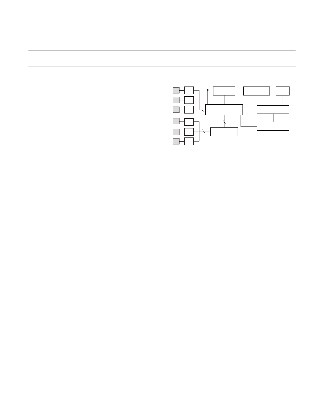
Three-Phase Energy
E-PULSE
ADSST-EM-2030
µCONTROLLER
OPTICAL PORT
OP AMP + MUX
COUNTER LCD DISPLAY RTC
PT
PT
PT
CT
CT
CT
POLY PHASE ENERGY METER USING THE ADSST-EM-2030
a
FEATURES
3-Phase, 4-Wire Metering IC
High Accuracy Support for 50 Hz/60 Hz, IEC1036
Design Accuracy:
0.5% over 5% of Ib to 6% of Ib
0.65% over 2% of Ib to 5% of Ib
Measures:
kWh
kW
rms Voltage of Each Phase
rms Current of Each Phase
Phase and Nonlinearity Compensation for CTs
Potentiometer-Free Design
SPI Communication for:
Data to Microcontroller
Calibration
Programmable E-Pulse
Drive for:
Electromechanical Counter
2-Phase Stepper Motor Counter
Low Power (50 mW Typ)
Meter Chipset
ADSST-EM-2030
FUNCTIONAL BLOCK DIAGRAM
*
GENERAL DESCRIPTION
ADSST-EM-2030 is a highly accurate and low cost phase
energy measurement IC intended to be used in 3-phase, 4-wire
systems. When used with an op amp and a multiplexer, the
ADSST-EM-2030 surpasses the accuracy requirement of the
IEC1036 standard.
ADSST-EM-2030 is a MicroConverter
troller, 6-channel, 12-bit ADC, SPI port, program memory and
Flash for storage of constants. The only analog circuitry used in
ADSST-EM-2030 is the ADC. All other signal processing is carried
out in digital domain. This provides superior accuracy over extreme
environmental conditions and time.
ADSST-EM-2030 can drive an electromechanical counter or a
2-phase stepper motor counter, or can be interfaced to a
microcontroller to build a feature-rich meter with LCD, maximum
demand, time of use, and communication.
*Protected by U.S.Patent No. 5,969,657; other patents pending.
MicroConverter is a registered trademark of Analog Devices.
REV. 0
Information furnished by Analog Devices is believed to be accurate and
reliable. However, no responsibility is assumed by Analog Devices for its
use, nor for any infringements of patents or other rights of third parties that
may result from its use. No license is granted by implication or otherwise
under any patent or patent rights of Analog Devices.
®
consisting of a microcon-
Ratio, phase, and nonlinearity errors of the CTs are compensated
for by using software. This reduces the cost of CTs and reduces
calibration time caused by unreliable potentiometers.
Because the ADSST-EM-2030 is a low power device, it can be
powered by a simple R-C power supply, reducing the cost of
operation.
ADSST-EM-2030 supplies average real power information on
the low frequency outputs F1 and F2. These logic outputs can
be used to drive an electromechanical counter. The CF logic pin
gives the instantaneous real power information. This output is
intended to be used for calibration.
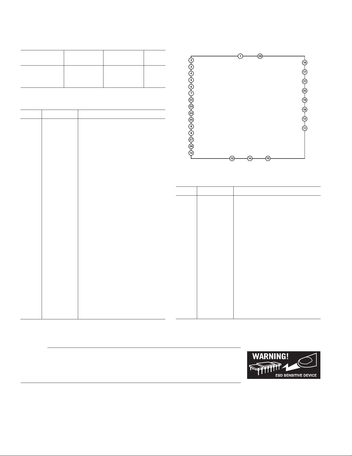
ADSST-EM-2030 is available in a 28-lead SSOP package.
One Technology Way, P.O. Box 9106, Norwood, MA 02062-9106, U.S.A.
Tel: 781/329-4700 www.analog.com
Fax: 781/326-8703 © Analog Devices, Inc., 2002
Page 2
ADSST-EM-2030
ORDERING GUIDE
Model Temperature Package Package
Range Description Option
ADSST-EM-2030 –40°C to +85°C Tiny Shrink RU–28
Small Outline
Package
PIN FUNCTION DESCRIPTION
Pin No. Mnemonic Description
1 DGND Digital Ground
2DLOAD Used to Enable Serial Download of
Program Memory
3GAIN 1 Logic Channels Output for
Multiplexer to Switch Gain for
A-Phase Current
4GAIN 2 Logic Channels Output for
Multiplexer to Switch Gain for
B-Phase Current
5 TAMP Logic Output Indicating that One
More Current Is Reversed
6CFCalibration Frequency Logic Output.
This gives instantaneous real power
information and can be used for
calibration.
7GAIN 3 Logic Channels Output for
Multiplexer to Switch Gain for
C-Phase Current
8, 9 F1, F2 Low Frequency Logic Outputs. F1
and F2 provide average real power
information. The logic outputs can
be used to drive electromechanical
counters and 2-phase stepper motors.
10 RESET System Reset
11 APHV A-Phase Voltage Input
12 APHC A-Phase Current Input
13 AVDD Analog Positive Supply
14 AGND Analog Ground
15 AGND Analog Ground
16 VREF Input for External Voltage Reference
PIN CONFIGURATION
DLOAD
GAIN 1
GAIN 2
TA M P
CF
GAIN 3
SS
MISO
MOSI
SCLK
F1
F2
XTAL2
XTAL1
RESET
DGND DVDD
AV DD
VREF
CREF
CPHC
CPHV
BPHC
BPHV
APHC
APHV
AGND AGND
PIN FUNCTION DESCRIPTION (continued)
Pin No. Mnemonic Description
17 CREF Filter Capacitor for Reference
18 BPHV B-Phase Voltage Input
19 BPHC B-Phase Current Input
20 CPHV C-Phase Voltage Input
21 CPHC C-Phase Current Input
22 SS This Logic Signal conveys to ADSST-
EM-2030 that data transfer on SPI is
requested.
23 MISO Data Output on SPI from
ADSST-EM-2030
24 MOSI
25 SCLK Clock for SPI. This clock is generated
by an external microcontroller when
the data transfer to or from ADSST-
EM-2030 takes place.
26 XTAL1 Crystal Oscillator
27 XTAL2 Crystal Oscillator
28 DVDD Digital Positive Supply
CAUTION
ESD (electrostatic discharge) sensitive device. Electrostatic charges as high as 4000 V readily accumulate
on the human body and test equipment and can discharge without detection. Although the ADSSTEM-2030 features proprietary ESD protection circuitry, permanent damage may occur on devices
subjected to high energy electrostatic discharges. Therefore, proper ESD precautions are recommended
to avoid performance degradation or loss of functionality.
REV. 0–2–
Page 3
ADSST-EM-2030
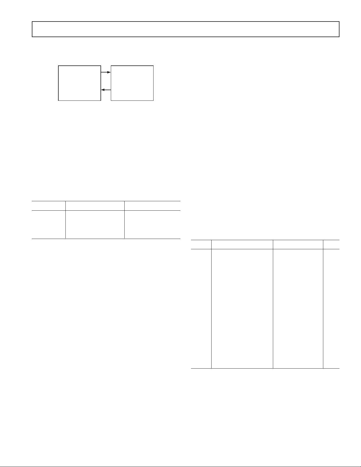
SERIAL PERIPHERAL INTERFACE (SPI)
The SPI bus available on the ADSST-EM-2030 is useful to
communicate to an external microcontroller as shown in Figure 1.
SLAVE
ADSST-EM-2030
MASTER
MICROCONTROLLER
Figure 1. SPI Communication between ADSST-EM-2030
and Microcontroller
Here, the microcontroller functions as master and the ADSSTEM-2030 is a slave for this protocol. Using this communication
port, the microcontroller will be able to read and write to the
ADSST-EM-2030 to perform the following functions:
•
Calibrate the meter
•
Configure the ADSST-EM-2030 chipset
•
Read measured parameters from the ADSST-EM-2030 chipset
Four pins are used on the ADSST-EM-2030 chipset for the
communication, and are shown Table I.
Table I. Pin Description for SPI Communication Port
Pin No. Mnemonic Description
22 SS Select
23 MISO Output
24 MOSI Input
25 SCLK SPI Clock
TIMING SPECIFICATIONS
This section contains timing information for the ADSST-EM2030 chipset.
General Notes
Use the exact timing information given. Do not attempt to
derive parameters from the addition or subtraction of others.
While addition or subtraction would yield meaningful results for
an individual device, the values given in this data sheet reflect
statistical variations and worst cases. Consequently, parameters
cannot be added up meaningfully to derive longer times.
Timing Notes
Switching characteristics specify how the processor changes its
signals. Designers have no control on this timing—circuitry external to the processor must be designed for compatibility with these
signal characteristics. These characteristics can be used to ensure
that any timing requirement of a microcontroller connected to
the chipset is satisfied.
Timing requirements apply to signals that are controlled by circuitry
external to the chipset, such as the data input for a read operation.
Timing requirements guarantee that the chipset operates correctly with the external microcontroller.
Data Access
Data can be written or read to the ADSST-EM-2030 chipset only
when the SS pin is low. Since the chipset is a slave, the external
controller must bring the SS pin low, the SCLK clock should be
sent to clock in or clock out the data. For sending the data to the
chipset, data should be sent on MOSI pin; for receiving the data
from the chipset, data should be collected on MISO pin.
With the external microcontroller as the master for the SPI
communication, the microcontroller should send eight successive clocks to the ADSST-EM-2030 every 5 ms. At this instant,
the microcontroller may either send a command or data or may
receive an acknowledgment followed by data from the chipset.
The ADSST-EM-2030 maintains a time gap of 5 ms between
transmission of two successive bytes to or from the microcontroller.
This helps in avoiding clashing o f interrupts while the chipset
and the microcontroller are executing their respective tasks.
Table II. SPI Pin Timings
Timing Parameter Min Typ Max Unit
t
SS
t
SC
SS to SCLOCK Edge 0 ns
SCLOCK Low
Pulsewidth 300 ns
t
SH
SCLOCK High
Pulsewidth 300 ns
t
DAV
Data Output Valid
after SCLOCK Edge 50 ns
t
DSU
Data Input Setup Time
before SCLOCK Edge 100 ns
t
DHD
Data Input Hold Time
before SCLOCK Edge 100 ns
t
t
t
t
t
DF
DR
SR
SF
SFS
Data Output Fall Time 10 25 ns
Data Output Rise Time 10 25 ns
SCLOCK Rise Time 10 25 ns
SCLOCK Fall Time 10 25 ns
SS High after
SCLOCK Edge 0 ns
REV. 0
–3–
Page 4
ADSST-EM-2030
SS
t
SS
t
DF
SCLK
t
SFS
MISO
MOSI
SCLOCK
SS
t
SH
t
DAV
t
SC
MSB
MSB
t
DSUtDHD
t
DF
t
DR
BITS6–1 LSB
BITS 6–1
Figure 2. SPI Communication Port Timing
t
SR
t
SF
LSB
SAMPLE INPUT
DATA OUTPUT
SPI INTERRUPT
FOR 8712S
MSB BIT 6 BIT 5 BIT 4 BIT 3 BIT 2 BIT 1 LSB ?
Figure 3. SPI Timing for Data Transmission Byte
SPI FUNCTIONS
Three specific functions can be performed on the SPI communication port on the ADSST-EM-2030 chipset:
Data Read—The external microcontroller can read the data
from the ADSST-EM-2030 by sending specific commands; this
includes metering data, constants, and so on.
Data Write—The external microcontroller can send data to the
ADSST-EM-2030 to be stored in its internal nonvolatile memory;
this includes calibration and configuration constants, and so on.
Special Commands—The external microcontroller can send
special commands to the ADSST-EM-2030 for performing specific
functions. These commands do not have any data.
Data Read
The microcontroller being the master for the SPI communication,
has to send the desired commands for getting data from ADSSTEM-2030. For the data transfer to take place, the following
sequence of operations must take place:
1. The microcontroller should send the specific command to
the ADSST-EM-2030 chipset to read the desired data.
2. The ADSST-EM-2030 will first respond with an acknowledgment to the microcontroller within 5 ms that it has
received the command. To send the acknowledgment, the
ADSST-EM-2030 adds 0x30 to the received command,
and which is then sent back to the microcontroller.
REV. 0–4–
Page 5

ADSST-EM-2030
3. If the microcontroller does not get this acknowledgment from the
ADSST-EM-2030 within 5 ms then the microcontroller may
transmit this command to read the same data again.
4. After being sensed by the microcontroller, the ADSST-EM-2030
sends an acknowledgment to the microcontroller, the chipset
then prepares a packet of 10 bytes of requested data and starts
transmitting the bytes one by one at intervals of 5 ms. This
packet of 10 bytes also includes a header as the first byte of the
packet and checksum as the last byte.
5. The microcontroller can strip the data from this packet, compute
the checksum, and compare it with the last byte in the packet.
If the checksum does not match, the microcontroller should
then send the command again to ADSST-EM-2030 chipset.
The complete process of reading a packet of data should take
60 ms. The next command from the microcontroller to the
ADSST-EM-2030 can be sent immediately after receipt of data
or wait for the desired amount of time. The amount of time the
microcontroller should wait for the next command to be sent to
the ADSST-EM-2030 is purely dependent on the execution
of other functions on the microcontroller. It may be sufficient
for the microcontroller to collect data from the chipset after
Table III. Read Commands to ADSST-EM-2030 on SPI
Function ADSST-EM-2030 from C from ADSST-EM-2030
CONSTANTS
GAIN CALIBRATION CONSTANTS
Read Voltage Gain Constants 0x01 6
Read Low Gain Current Constants 0x02 6
Read High Gain Current Constants 0x03 6
POWER CALIBRATION CONSTANTS AT HIGH CURRENT RANGE
A-Phase Power Constant at High Current
(Including E-Pulse and Counter Pulse Constant) 0x07 4
B-Phase Power Constant at High Current 0x09 2
C-Phase Power Constant at High Current 0x0B 2
POWER CALIBRATION CONSTANTS AT LOW CURRENT RANGE
A-Phase Power Constant at Low Current 0x06 2
B-Phase Power Constant at Low Current 0x08 2
C-Phase Power Constant at Low Current 0x0A 2
PHASE COMPENSATION COEFFICIENTS
Read A-, B-, and C-Phase Coefficients 0x15 6
DC OFFSET CONSTANTS
Read DC Offset Constants 0x0E 6
INSTANTANEOUS PARAMETERS
Read Voltages for Phase A, B, and C 0x0F 6
Read Currents for Phase A, B, and C 0x10 6
Read Energy and Power for Phase A, B, and C 0x11 8
every second. The remaining time may be used by the microcontroller to perform other housekeeping functions.
For example, if the command sent by the microcontroller is 0x01,
the ADSST-EM-2030 adds 0x30 to it, making it 0x31, and sends
this to the microcontroller as an acknowledgment.
The data packet structure created by the ADSST-EM-2030 has
10 bytes. The first byte is a packet start byte (0xEE) and the last
byte is a checksum byte.
< START of Packet (0xEE) >< 8 Bytes of Data>
< CHECKSUM >
The checksum is calculated by adding the first nine bytes, including the packet start byte.
st
CHECKSUM = 1
Table III shows various commands that can be sent to the ADSSTEM-2030 chipset by the microcontroller on the SPI communication
port. The chipset returns a specific number of bytes for each data
parameter specified, in the data column of the table. The data
that can be read from the chipset could be calibration constants
or instantaneous data.
Command to Number of Data Bytes
nd
+ 2
+ ...... ...... + 9th Byte
REV. 0
–5–
Page 6
ADSST-EM-2030
Data Structure in the Packet
The ADSST-EM-2030 sends out eight bytes of data for every command. The last bytes of a parameter with a 6-byte structure are
kept at zero and should be neglected.
Table IV. Byte Wise Packet Data Structure for Voltage Gain Constants
Command to ADSST-EM-2030: 0x01
Acknowledgment from ADSST-EM-2030: 0x31
123456789 01
BPSSMVASLVASMVBSLVBSMVCSLVCVLNVLNMUSC
Byte No. Name Description
1 SPB Start Packet Byte (0xEE)
2 AVMS Voltage Constant for A-Phase – MSB
3 AVLS Voltage Constant for A-Phase – LSB
4 BVMS Voltage Constant for B-Phase – MSB
5 BVLS Voltage Constant for B-Phase – LSB
6 CVMS Voltage Constant for C-Phase – MSB
7 CVLS Voltage Constant for C-Phase – LSB
8 NLV No Legal Value (0x00)
9 NLV No Legal Value (0x00)
10 CSUM Checksum
Table V. Byte Wise Packet Data Structure for Low Gain Current Constants
Command to ADSST-EM-2030: 0x02
Acknowledgment from ADSST-EM-2030: 0x32
123456789 01
BPSMLIALLIAMLIBLLIBMLICLLICVLNVLNMUSC
Byte No. Name Description
1 SPB Start Packet Byte (0xEE)
2 AILM Current Constant for A-Phase – Low Gain – MSB
3 AILL Current Constant for A-Phase – Low Gain – LSB
4 BILM Current Constant for B-Phase – Low Gain – MSB
5 BILL Current Constant for B-Phase – Low Gain – LSB
6 CILM Current Constant for C-Phase – Low Gain – MSB
7 CILL Current Constant for C-Phase – Low Gain – LSB
8 NLV No Legal Value (0x00)
9 NLV No Legal Value (0x00)
10 CSUM Checksum
Table VI. Byte Wise Packet Data Structure for High Gain Current Constants
Command to ADSST-EM-2030: 0x03
Acknowledgment from ADSST-EM-2030: 0x33
123456789 01
BPSMHIALHIAMHIBLHIBMHICLHICVLNVLNMUSC
Byte No. Name Description
1 SPB Start Packet Byte (0xEE)
2 AIHM Current Constant for A-Phase – High Gain – MSB
3 AIHL Current Constant for A-Phase – High Gain – LSB
4 BIHM Current Constant for B-Phase – High Gain – MSB
5 BIHL Current Constant for B-Phase – High Gain – LSB
6 CIHM Current Constant for C-Phase – High Gain – MSB
7 CIHL Current Constant for C-Phase – High Gain – LSB
8 NLV No Legal Value (0x00)
9 NLV No Legal Value (0x00)
10 CSUM Checksum
REV. 0–6–
Page 7

ADSST-EM-2030
Table VII. Byte Wise Packet Data Structure for Power Constants at High Current for Phase A
Command to ADSST-EM-2030: 0x07
Acknowledgment from ADSST-EM-2030: 0x37
123456789 01
BPSMHAPLHAPCPECPCVLNVLNVLNVLNMUSC
Byte No. Name Description
1 SPB Start Packet Byte (0xEE)
2 PAHM Power Constant for A-Phase, High Current – MSB
3 PAHL Power Constant for A-Phase, High Current – LSB
4 EPC E-Pulse Constant in Pulses per kWh (1 = 1600, 2 = 800,
3 = 400, and 4 = 200), Default Value = 1
5 CPC Counter Pulse Constant in Pulses per kWh (1 = 200 and
2 = 400), Default Value = 1
6 NLV No Legal Value (0x00)
7 NLV No Legal Value (0x00)
8 NLV No Legal Value (0x00)
9 NLV No Legal Value (0x00)
10 CSUM Checksum
Table VIII. Byte Wise Packet Data Structure for Power Constants at High Current for Phase B
Command to ADSST-EM-2030: 0x09
Acknowledgment from ADSST-EM-2030: 0x39
123456789 01
BPSMHBPLHBPVLNVLNVLNVLNVLNVLNMUSC
Byte No. Name Description
1 SPB Start Packet Byte (0xEE)
2 PBHM Power Constant for B-Phase, High Current – MSB
3 PBHL Power Constant for B-Phase, High Current – LSB
4 NLV No Legal Value (0x00)
5 NLV No Legal Value (0x00)
6 NLV No Legal Value (0x00)
7 NLV No Legal Value (0x00)
8 NLV No Legal Value (0x00)
9 NLV No Legal Value (0x00)
10 CSUM Checksum
Table IX. Byte Wise Packet Data Structure for Power Constants at High Current for Phase C
Command to ADSST-EM-2030: 0x0B
Acknowledgment from ADSST-EM-2030: 0x3B
123456789 01
BPSMHCPLHCPVLNVLNVLNVLNVLNVLNMUSC
Byte No. Name Description
1 SPB Start Packet Byte (0xEE)
2 PCHM Power Constant for C-Phase, High Current – MSB
3 PCHL Power Constant for C-Phase, High Current – LSB
4 NLV No Legal Value (0x00)
5 NLV No Legal Value (0x00)
6 NLV No Legal Value (0x00)
7 NLV No Legal Value (0x00)
8 NLV No Legal Value (0x00)
9 NLV No Legal Value (0x00)
10 CSUM Checksum
REV. 0
–7–
Page 8

ADSST-EM-2030
Table X. Byte Wise Packet Data Structure for Power Constants at Low Current for Phase A
Command to ADSST-EM-2030: 0x06
Acknowledgment from ADSST-EM-2030: 0x36
Byte No. Name Description
1 SPB Start Packet Byte (0xEE)
2 PALM Power Constant for A-Phase, Low Current – MSB
3 PALL Power Constant for A-Phase, Low Current – LSB
4 NLV No Legal Value (0x00)
5 NLV No Legal Value (0x00)
6 NLV No Legal Value (0x00)
7 NLV No Legal Value (0x00)
8 NLV No Legal Value (0x00)
9 NLV No Legal Value (0x00)
10 CSUM Checksum
Table XI. Byte Wise Packet Data Structure for Power Constants at Low Current for Phase B
Command to ADSST-EM-2030: 0x08
Acknowledgment from ADSST-EM-2030: 0x38
123456789 01
BPSMLAPLLAPVLNVLNVLNVLNVLNVLNMUSC
123456789 01
BPSMLBPLLBPVLNVLNVLNVLNVLNVLNMUSC
Byte No. Name Description
1 SPB Start Packet Byte (0xEE)
2 PBLM Power Constant for B-Phase, Low Current – MSB
3 PBLL Power Constant for B-Phase, Low Current – LSB
4 NLV No Legal Value (0x00)
5 NLV No Legal Value (0x00)
6 NLV No Legal Value (0x00)
7 NLV No Legal Value (0x00)
8 NLV No Legal Value (0x00)
9 NLV No Legal Value (0x00)
10 CSUM Checksum
Table XII. Byte Wise Packet Data Structure for Power Constants at Low Current for Phase C
Command to ADSST-EM-2030: 0x0A
Acknowledgment from ADSST-EM-2030: 0x3A
123456789 01
BPSMLCPLLCPVLNVLNVLNVLNVLNVLNMUSC
Byte No. Name Description
1 SPB Start Packet Byte (0xEE)
2 PCLM Power Constant for C-Phase, Low Current – MSB
3 PCLL Power Constant for C-Phase, Low Current – LSB
4 NLV No Legal Value (0x00)
5 NLV No Legal Value (0x00)
6 NLV No Legal Value (0x00)
7 NLV No Legal Value (0x00)
8 NLV No Legal Value (0x00)
9 NLV No Legal Value (0x00)
10 CSUM Checksum
REV. 0–8–
Page 9

Table XIII. Byte Wise Packet Data Structure for Phase Compensation Coefficients
Command to ADSST-EM-2030: 0x15
Acknowledgment from ADSST-EM-2030: 0x45
123456789 01
BPSAGPASPBGPBSPCGPCSPVLNVLNMUSC
Byte No. Name Description
1 SPB Start Packet Byte (0xEE)
2 PGA Phase Constant for Low Current – Phase A
3 PSA Phase Constant for High Current – Phase A
4 PGB Phase Constant for Low Current – Phase B
5 PSB Phase Constant for High Current – Phase B
6 PGC Phase Constant for Low Current – Phase C
7 PSC Phase Constant for High Current – Phase C
8 NLV No Legal Value (0x00)
9 NLV No Legal Value (0x00)
10 CSUM Checksum
Table XIV. Byte Wise Packet Data Structure for DC Offset Constants
Command to ADSST-EM-2030: 0x0E
Acknowledgment from ADSST-EM-2030: 0x3E
123456789 01
BPSMADLADMBDLBDMCDLCDVLNVLNMUSC
ADSST-EM-2030
Byte No. Name Description
1 SPB Start Packet Byte (0xEE)
2 DAM DC Offset for Phase A - MSB
3 DAL DC Offset for Phase A – LSB
4 DBM DC Offset for Phase B – MSB
5 DBL DC Offset for Phase B – LSB
6 DCM DC Offset for Phase C – MSB
7 DCL DC Offset for Phase C – LSB
8 NLV No Legal Value (0x00)
9 NLV No Legal Value (0x00)
10 CSUM Checksum
Table XV. Byte Wise Packet Data Structure while Reading Instantaneous Voltages in Volts
Command to ADSST-EM-2030: 0x0F
Acknowledgment from ADSST-EM-2030: 0x3F
Voltage Value Resolution: Two Decimal Points
123456789 01
repmaT
BPSMAVLAVMBVLBVMCVLCV
Byte No. Name Description
1 SPB Start Packet Byte (0xEE)
2 VAM Voltage for Phase A – MSB
3 VAL Voltage for Phase A – LSB
4 VBM Voltage for Phase B – MSB
5 VBL Voltage for Phase B – LSB
6 VCM Voltage for Phase C – MSB
7 VCL Voltage for Phase C – LSB
8 Tamper Info 0 bit: A – CT Reversal
First Bit: B – CT Reversal
Second Bit: C – CT Reversal
Third Bit: Phase Sequence Error
9 Not used
10 CSUM Checksum
toN
ofnI
desu
MUSC
REV. 0
–9–
Page 10

ADSST-EM-2030
Table XVI. Byte Wise Packet Data Structure While Reading Instantaneous Current in Amperes
Command to ADSST-EM-2030: 0x10
Acknowledgment from ADSST-EM-2030: 0x40
Current value resolution: Three Decimal Points
Byte No. Name Description
1 SPB Start Packet Byte (0xEE)
2 IAM Current for Phase A – MSB
3 IAL Current for Phase A – LSB
4 IBM Current for Phase B – MSB
5 IBL Current for Phase B – LSB
6 ICM Current for Phase C – MSB
7 ICL Current for Phase C – LSB
8 ACTR Freq (MSB)
9 ACTR Freq (LSB)
10 CSUM Checksum
Table XVII. Byte Wise Packet Data Structure While Reading Instantaneous Power and Energy
Command to ADSST-EM-2030: 0x11
Acknowledgment from ADSST-EM-2030: 0x41
Power Value (in kW) Resolution: Five Decimal Points
Energy Value (in kWh) Resolution: Four Decimal Points
123456789 01
BPSMAILAIMBILBIMCILCIRTCARTCAMUSC
123456789 01
BPS1TP2TP3TP4TP1TE2TE3TE4TEMUSC
Byte No. Name Description
1 SPB Start Packet Byte (0xEE)
2 PT1 Total Power First Byte – MSB
3 PT2 Total Power Second Byte
4 PT3 Total Power Third Byte
5 PT4 Total Power Fourth Byte – LSB
6 ET1 Total Energy First Byte – MSB
7 ET2 Total Energy Second Byte
8 ET3 Total Energy Third Byte
9 ET4 Total Energy Fourth Byte – LSB
10 CSUM Checksum
REV. 0–10–
Page 11

ADSST-EM-2030
Data Interpretation
The data sent by ADSST-EM-2030 is in Hex, and the microcontroller has to convert this and place the decimal point at the correct
place for display.
Table XVIII. Interpretation of the Voltage Data
The data sent for Voltage has a resolution up to two decimal places.
Each Phase Voltage Data
Hex Value (2 Byte) Decimal Value Voltage
5A10h 23056 230.56 V
Table XIX. Interpretation of the Current Data
The data sent for Current has a resolution up to three decimal places.
Each Phase Current Data
Hex Value (2 Byte) Decimal Value Current
278Bh 10123 10.123 A
Table XX. Interpretation of the Power Data
The data sent for Power has a resolution up to five decimal places.
Each Phase Power Data
Hex Value (4 Byte) Decimal Value Power
0D1C4Ah 859210 8.59210 kW
Table XXI. Interpretation of the Energy Data
The data sent for Energy has a resolution up to four decimal places.
Each Phase Energy Data
Hex Value (4 Byte) Decimal Value Energy
0D1C4Ah 859210 85.9210 kWh
Data Write
Because microcontroller is the master for the SPI communication,
it has to send the desired commands for sending the data to the
ADSST-EM-2030. For the data transfer to take place, the following
sequence of operation has to occur:
1. The microcontroller should send the packet of 10 bytes including
the specific command to the ADSST-EM-2030 chipset to write
the desired data. Thus, the packet of 10 bytes includes a header
as the first byte of the packet, a specific command for write
data, and checksum as the last byte.
2. The ADSST-EM-2030 will receive the bytes one by one in
intervals of 5 ms.
3. The ADSST-EM-2030 strips the data from this packet, computes
the checksum and compares it with the last byte in the packet.
If the checksum does not match, the microcontroller should
send the command to the ADSST-EM-2030 chipset again, else
the ADSST-EM-2030 sends the acknowledgment of receipt of
all the bytes to be written.
4. To send the acknowledgment, the ADSST-EM-2030 adds
0x30 to the received command, which is then sent back to the
microcontroller.
5. If the microcontroller does not get this acknowledgment from the
ADSST-EM-2030 by 5 ms, then the microcontroller may
transmit this command to write the same data again.
The complete process of writing a packet of data should take 60 ms.
The next command from the microcontroller to the ADSST-EM2030 can be sent immediately after receipt of data or wait for the
desired amount of time. The amount of time the microcontroller
waits for the next command to be sent to ADSST-EM-2030 is
purely dependent on the execution of other functions on the
microcontroller. It may be sufficient for the microcontroller to
collect data from the chipset after every one second. The
remaining time may be used by the microcontroller to perform
other housekeeping functions.
For example, if the command sent by the microcontroller is
0x01; the ADSST-EM-2030 adds 0x30 to it, making it 0x31,
and sends this to the microcontroller as an acknowledgment.
The data packet structure created by the ADSST-EM-2030 has
10 bytes. The first byte is a packet start byte (0xEE), and the
last byte is a checksum byte.
< START of Packet (0xEE) ><Command of 1 Byte>
< 7 Bytes of Data><CHECKSUM >
The checksum is calculated by adding the first nine bytes including
the Packet start byte.
st
CHECKSUM = 1
nd
+ 2
+ ...... ...... + 9th Byte
REV. 0
–11–
Page 12

ADSST-EM-2030
Table XXII shows various commands that can be sent to the ADSST-EM-2030 chipset by the microcontroller on the SPI communication port. The chipset writes the specific number of bytes for each data parameter specified in the data column of the table. The data
that can be written to the chipset could be calibration constants.
Table XXII. Interpretation of the Energy Data
Command to
Data ADSST-EM-2030 Data Bytes
GAIN CALIBRATION
Voltage Coefficient 0x81 6
Current Low Gain Coefficient 0x82 6
Current High Gain Coefficient 0x83 6
POWER CALIBRATION CONSTANTS AT HIGH CURRENT RANGE
A-Phase Power Constant at High Current
(with E-Pulse and Counter Pulse) 0x87 4
B-Phase Power Constant at High Current 0x89 2
C-Phase Power Constant at High Current 0x8B 2
POWER CALIBRATION CONSTANTS AT LOW CURRENT RANGE
A-Phase Power Constant at Low Current 0x86 2
B-Phase Power Constant at Low Current 0x88 2
C-Phase Power Constant at Low Current 0x8A 2
PHASE COMPENSATION COEFFICIENTS
A-, B-, C-Phase Coefficient 0x95 6
Data Structure in the Packet
The ADSST-EM-2030 sends out seven bytes of data for every command. The last bytes of a 6-byte structure are kept at zero and
should be neglected.
Table XXIII. Byte Wise Packet Data Structure for Voltage Gain Constants
Command to ADSST-EM-2030: 0x81
Acknowledgment from ADSST-EM-2030: 0xB1
12 3 4 5 6 78901
BPSVWCMVAWLVAWMVBWLVBWMVCWLVCWVLNMUSC
Byte No. Name Description
1 SPB Start Packet Byte (0xEE)
2 CWV Command to Write Voltage Constant
3 WAVM Voltage Constant for A-Phase – MSB
4 WAVL Voltage Constant for A-Phase – LSB
5 WBVM Voltage Constant for B-Phase – MSB
6 WBVL Voltage Constant for B-Phase – LSB
7 WCVM Voltage Constant for C-Phase – MSB
8 WCVL Voltage Constant for C-Phase – LSB
9 NLV No Legal Value (0x00)
10 CSUM Checksum
REV. 0–12–
Page 13

ADSST-EM-2030
Table XXIV. Byte Wise Packet Data Structure for Low Gain Current Constants
Command to ADSST-EM-2030: 0x82
Acknowledgment from ADSST-EM-2030: 0xB2
12 3 4 5 6 78901
BPSIWCMIAWLIAWMIBWLIBWMICWLICWVLNMUSC
Byte No. Name Description
1 SPB Start Packet Byte (0xEE)
2 CWI Command to Write Low Gain Current Constant
3 WAIM Current Constant for A-Phase – Low Gain – MSB
4 WAIL Current Constant for A-Phase – Low Gain – LSB
5 WBIM Current Constant for B-Phase – Low Gain – MSB
6 WBIL Current Constant for B-Phase – Low Gain – LSB
7 WCIM Current Constant for C-Phase – Low Gain – MSB
8 WCIL Current Constant for C-Phase – Low Gain – LSB
9 NLV No Legal Value (0x00)
10 CSUM Checksum
Table XXV. Byte Wise Packet Data Structure for High Gain Current Constants
Command to ADSST-EM-2030: 0x83
Acknowledgment from ADSST-EM-2030: 0xB3
12 3 4 5 6 78901
BPSIHWCMIHAWLIHAWMIHBWLIHBWMIHCWLIHCWVLNMUSC
Byte No. Name Description
1 SPB Start Packet Byte (0xEE)
2 CWHI Command to Write High Gain Current Constant
3 WAHIM Current Constant for A-Phase – High Gain – MSB
4 WAHIL Current Constant for A-Phase – High Gain – LSB
5 WBHIM Current Constant for B-Phase – High Gain – MSB
6 WBHIL Current Constant for A-Phase – High Gain – LSB
7 WCHIM Current Constant for A-Phase – High Gain – MSB
8 WCHIL Current Constant for A-Phase – High Gain – LSB
9 NLV No Legal Value (0x00)
10 CSUM Checksum
Table XXVI. Byte Wise Packet Data Structure for Power Constants at High Current for Phase A
Command to ADSST-EM-2030: 0x87
Acknowledgment from ADSST-EM-2030: 0xB7
12 3 4 56789 01
BPSHPAWCNHAPWLHAPWCPECPCVLNVLNVLNMUSC
Byte No. Name Description
1 SPB Start Packet Byte (0xEE)
2 CWAPH Command to Write Power Constant for A-Phase at High Current
3 WPAHM Power Constant for A-Phase, High Current – MSB
4 WPAHL Power Constant for A-Phase, High Current – LSB
5 EPC E-Pulse Constant in Pulses per kWh (1 = 1600, 2 = 800,
3=400, and 4 = 200), Default Value = 1
6 CPC Counter Pulse Constant in Pulses per kWh (1 = 200 and
2=400), Default Value = 1
7 NLV No Legal Value (0x00)
8 NLV No Legal Lalue (0x00)
9 NLV No Legal Value (0x00)
10 CSUM Checksum
REV. 0
–13–
Page 14

ADSST-EM-2030
Table XXVII. Byte Wise Packet Data Structure for Power Constants at High Current for Phase B
Command to ADSST-EM-2030: 0x89
Acknowledgment from ADSST-EM-2030: 0xB9
Byte No. Name Description
1 SPB Start Packet Byte (0xEE)
2 CWBPH Command to Write Power Constant for B-Phase at
3 WPBHM Power Constant for B-Phase, High Current – MSB
4 WPBHL Power Constant for B-Phase, High Current – LSB
5 EPC No Legal Value (0x00)
6 CPC No Legal Value (0x00)
7 NLV No Legal Value (0x00)
8 NLV No Legal Value (0x00)
9 NLV No Legal Value (0x00)
10 CSUM Checksum
Table XXVIII. Byte Wise Packet Data Structure for Power Constants at High Current Phase C
Command to ADSST-EM-2030: 0x8B
Acknowledgment from ADSST-EM-2030: 0xBB
12 3 456789 01
BPSHPBWCMHBPWLHBPWCPECPCVLNVLNVLNMUSC
High Current
12 3 45678901
BPSHPCWCMHCPWLHCPWCPECPCVLNVLNVLNMUSC
Byte No. Name Description
1 SPB Start Packet Byte (0xEE)
2CWCPH Command to Write Power Constant for C Phase at
High Current
3 WPCHM Power Constant for C-Phase, High Current – MSB
4 WPCHL Power Constant for C-Phase, High Current – LSB
5 EPC No Legal Value (0x00)
6 CPC No Legal Value (0x00)
7 NLV No Legal Value (0x00)
8 NLV No Legal Value (0x00)
9 NLV No Legal Value (0x00)
10 CSUM Checksum
Table XXIX. Byte Wise Packet Data Structure for Power Constants at Low Current for Phase A
Command to ADSST-EM-2030: 0x86
Acknowledgment from ADSST-EM-2030: 0xB6
12 3 456789 01
BPSLPAWCMLAPWLLAPWVLNVLNVLNVLNVLNMUSC
Byte No. Name Description
1 SPB Start Packet Byte (0xEE)
2 CWAPL Command to Write Power Constant for A-Phase at
Low Current
3 WPALM Power Constant for A-Phase, Low Current – MSB
4 WPALL Power Constant for A-Phase, Low Current – LSB
5 NLV No Legal Value (0x00)
6 NLV No Legal Value (0x00)
7 NLV No Legal Value (0x00)
8 NLV No Legal Value (0x00)
9 NLV No Legal Value (0x00)
10 CSUM Checksum
REV. 0–14–
Page 15

ADSST-EM-2030
Table XXX. Byte Wise Packet Data Structure for Power Constants at Low Current for Phase B
Command to ADSST-EM-2030: 0x88
Acknowledgment from ADSST-EM-2030: 0xB8
12 3 4 56789 01
BPSLPBWCMLBPWLLBPWVLNVLNVLNVLNVLNMUSC
Byte No. Name Description
1 SPB Start Packet Byte (0xEE)
2 CWBPL Command to Write Power Constant for B-Phase at
Low Current
3 WPBLM Power Constant for B-Phase, Low Current – MSB
4 WPBLL Power Constant for B-Phase, Low Current – LSB
5 NLV No Legal Value (0x00)
6 NLV No Legal Value (0x00)
7 NLV No Legal Value (0x00)
8 NLV No Legal Value (0x00)
9 NLV No Legal Value (0x00)
10 CSUM Checksum
Table XXXI. Byte Wise Packet Data Structure for Power Constants at Low Current for Phase C
Command to ADSST-EM-2030: 0x8A
Acknowledgment from ADSST-EM-2030: 0xBA
12 3 4 567890101010101
BPSLPCWCMLCPWLLCPWVLNVLNVLNVLNVLNMUSCMUSC
MUSCMUSC
MUSC
Byte No. Name Description
1 SPB Start Packet Byte (0xEE)
2 CWCPL Command to Write Power Constant for C-Phase at
Low Current
3 WPCLM Power Constant for C-Phase, Low Current – MSB
4 WPCLL Power Constant for C-Phase, Low Current – LSB
5 NLV No Legal Value (0x00)
6 NLV No Legal Value (0x00)
7 NLV No Legal Value (0x00)
8 NLV No Legal Value (0x00)
9 NLV No Legal Value (0x00)
10 CSUM Checksum
Table XXXII. Byte Wise Packet Data Structure for Phase Compensation Coefficients
Command to ADSST-EM-2030: 0x95
Acknowledgment from ADSST-EM-2030: 0xC5
12 3 4 56789 01
BPSCPWCAGPWASPWBGPWBSPWCGPWCSPWVLNMUSC
Byte No. Name Description
1 SPB Start Packet Byte (0xEE)
2 CWPC Command to Write Phase Compensation Coefficients
3 WPGA Phase Constant for Low Current – Phase A
4 WPSA Phase Constant for High Current – Phase A
5 WPGB Phase Constant for Low Current – Phase B
6 WPSB Phase Constant for High Current – Phase B
7 WPGC Phase Constant for Low Current – Phase C
8 WPSC Phase Constant for High Current – Phase C
9 NLV No Legal Value (0x00)
10 CSUM Checksum
REV. 0
–15–
Page 16

ADSST-EM-2030
Special Data
The microcontroller sends some special commands to ADSST-EM-2030 for the special functions like dc offset calculation, initializing the
energies, and resetting the calibration constants. The packet sent by the microcontroller to the ADSST-EM-2030 contains only the command
byte and no data bytes. On receiving the packet of command, the ADSST-EM-2030 sends back the acknowledgment to the microcontroller by adding 0x30 to the command value. If the microcontroller does not get this acknowledgment from the ADSST-EM-2030
by 5 ms, then the microcontroller may transmit this command to write the same data again.
Table XXXIII shows special commands that can be sent to the ADSST-EM-2030 chipset by the microcontroller on the SPI communication port. The chipset sends back the acknowledgment for each command to the microcontroller. The functions that are done by the
chipset are dc offset calibration, initialization of energies, and resetting the calibration constants.
Table XXXIII. Special Commands to the ADSST-EM-2030 on SPI
Command to Acknowledgment to
Function ADSST-EM-2030 the Microcontroller Comment
DC OFFSET
Calculates DC
Calculate DC Offset 0x0D 0x3D Offset Constants
INITIALIZATION
Initializes the
Energy Initialize 0x16 0x46 Energy Values to Zero
RESET
Reset the Calibration
Constants to the
Reset Calibration 0x18 0x48 Default Values
Reset Calibration
To calibrate the meter using the ADSST-EM-2030, first reset
the calibration. By sending a command 0x18 on the SPI to the
ADSST-EM-2030, the chipset automatically resets the calibration.
Procedure
1. Power up the meter with standard voltage without any current
on the current channels.
2. Send 0x18 on the SPI.
DC Offset Calibration for Voltage and Current
The dc offset calibration takes care of the dc offset that may be
there in the signal path introduced by any of the front-end elements.
By sending 0x0D command on the SPI communication port to the
ADSST-EM-2030, the chipset performs calculation of dc offsets
on the voltage and current channels and stores the coefficients in
its flash memory. While the calibration is in progress, communication on SPI will not be accepted by the chipset.
Procedure
1. Power up the meter with standard voltage of all phases without
any current on the current channels.
2. Send 0x0D on the SPI to perform DC offset calibration.
3. Read back the coefficients on SPI by sending 0x0E to the
chipset.
Voltage Gain Calibration
The ADSST-EM-2030 enables software calibration of the voltage
channels to take care of tolerances for the passive components
used in the signal path.
Procedure
1. Power up the meter by setting the voltage source at 230 V on
all the three phases (say V
).
R
2. Send 0x01 command on the SPI to the chipset for reading
the voltage constants as C
, CVB, and C
VA
VC.
3. The ADSST-EM-2030 will return back six bytes of voltage
values for the three phases (V
, VB, and VC).
A
4. Compute the new constants on a PC or a calculator in Hex as:
V
R
=×C
′
VA
=×C
′
VB
=×C
′
VC
C
VA
V
A
V
R
C
VB
V
B
V
R
C
VC
V
C
5. These coefficients can then be written by sending the 0x81
command to the chipset on the SPI. Refer to Table XXIII for
the Write Data sequence. The coefficients are sent in the same
sequence as in the Table XXIII. This automatically stores the
voltage constants in the chipset’s internal nonvolatile memory.
6. To verify the coefficients, send 0x01 to the chipset to receive
the six bytes of data as voltage coefficients.
7. The default constants in the chipset for all the voltage channels
is 0x709C.
Current Calibration
The ADSST-EM-2030 enables software calibration of the current
channels to take care of tolerances for the passive components
used in the signal path.
Low Gain Current Calibration
1. Power up the meter by setting the current source at 60 amps
on all three phases (I
).
R
2. Send 0x02 command on the SPI to the chipset for reading
the current constants as: C
, CIB, and CIC.
IA
REV. 0–16–
Page 17

ADSST-EM-2030
3. The ADSST-EM-2030 will return back six bytes of current
values for the three phases: I
, IB, and IC.
A
4. Compute the new constants on a PC or a calculator in Hex as:
I
R
=×C
′
IA
=×C
′
IB
=×C
′
IC
C
IA
I
A
I
R
C
IB
I
B
I
R
C
IC
I
C
5. These coefficients can then be written by sending the 0x82
command to the chipset on the SPI. Refer to Table XXIV
for the Write Data sequence. The coefficients are sent in the
same sequence as in the Table XXIV. This automatically
stores the current constants in the chipsets’ internal nonvolatile
memory.
6. To verify the coefficients, send 0x02 to the chipset to receive
the six bytes of data as current coefficients.
7. The default constants in the chipset for all the low gain current
channels is 0x7000.
High Gain Current Calibration
1. Power up the meter by setting the current source at 5 amps
on all three phases (i
).
R
2. Send 0x03 command on the SPI to the chipset for reading
the current constants as: C
, CiB, and C
iA
iC .
3. The ADSST-EM-2030 will return back six bytes of current
values for the three phases (i
, iB, iC).
A
4. Compute the new constants on a PC or a calculator in Hex as:
i
R
=×C
′
iA
=×C
′
iB
=×C
′
iC
C
iA
i
A
i
R
C
iB
i
B
i
R
C
iC
i
C
5. These coefficients can then be written by sending the 0x83
command to the chipset on the SPI. Refer to Table XXV for
the Write Data sequence. The coefficients are sent in the same
sequence as in Table XXV. This automatically stores the
current constants in the chipset’s internal nonvolatile memory.
6. To verify the coefficients, send 0x03 to the chipset to receive
the six bytes of data as current coefficients.
7. The default constants in the chipset for all the high gain
current channels is 0x2300.
Power Calibration
The meter can now be calibrated for power for each phase. The
calculation requires the default constants that are stored in the
internal nonvolatile memory. Due to the chipset’s in-built feature
of performing automatic gain switching for the current channels,
the power needs to be calibrated at low gain (i.e., high currents)
and high gain (i.e., low currents). It is recommended that low
gain calibration is performed at I
performed at I
NOMINAL
/2. In the present example, the meter is
specified for 230 V operation with I
and high gain calibration is
MAX
at 60 amps.
MAX
Low Gain Power Calibration
The default power constant for all three phases at low gain is
0x3EE4. By sending commands such as 0x07, 0x09, and 0x0B
on the SPI, the chipset will send six bytes each, corresponding
to Phases A, B, and C.
Procedure
1. Power up the meter after setting the voltage at 230 V, current
at 60 amps and power factor at unity.
2. Read the default power constants for Phase A by sending 0x07
command on the SPI. The chipset will return six bytes, giving
the default constants P
for power constants for Phase A.
CA
3. Read the default constants for Phase B by sending 0x09
command on the SPI. The chipset will return six bytes,
giving the default constants P
for power constants for
CB
Phase B.
4. Read the default power constants for Phase C by sending 0x0B
command on the SPI. The chipset will return six bytes,
giving the default constants P
for power constants for
CC
Phase C.
5. Read the value of power as shown by the reference meter for
the three phases, say P
, PB, and PC.
A
6. If the voltage and current on the source have been set at
230 V and high current (60 amps), then the reference meter
should display for each phase a value of P
. Using this,
REF
calculate new constants as:
P
=×PP
′
CA CA
=×PP
′
CB CB
=×PP
′
CC CC
7. Send command 0x87 followed by P'
REF
P
A
P
REF
P
B
P
REF
P
C
value on the SPI. The
CA
chipset will accept the values and store these as power constants
for Phase A. Send command 0x89 followed by P'
command 0xB9 followed by P'
value. The chipset will store
CC
value and then
CB
these power constants for Phase B and Phase C respectively.
High Gain Power Calibration
The default power constants for all three phases at high gain
is 0xAA0. By sending commands such as 0x06, 0x08 and 0x0A
on SPI, the chipset will send six bytes each, corresponding to
Phase A, B, and C.
Procedure
1. Power up the meter after setting the voltage at 230 V, current
at 5 amps and power factor at unity.
2. Read the default power constants for Phase A by sending 0x06
command on the SPI. The chipset will return six bytes, giving
the default constants P
for Power constants for Phase A.
CA
3. Read the default constants for Phase B by sending 0x08
command on the SPI. The chipset will return six bytes, giving
the default constants P
for Power constants for Phase B.
CB
4. Read the default power constants for Phase C by sending 0x0A
command on the SPI. The chipset will return six bytes, giving
the default constants P
for Power constants for Phase C.
CC
5. Read the value of power as shown by the reference meter for
the three phases, say P
, PB, and PC.
A
REV. 0
–17–
Page 18

ADSST-EM-2030
6. If the voltage and current on the source have been set at
230 V and low current (5 amps), then the reference meter
should display for each phase a value, say P
. Calculate
REF
new constants as:
P
=×PP
′
CA CA
=×PP
′
CB CB
=×PP
′
CC CC
7. Send command 0x86 followed by P'
command 0x88 followed by P'
followed by P'
to save the power constants for high gain.
CC
REF
P
A
P
REF
P
B
P
REF
P
C
value on the SPI. Send
CA
value and then command 0x8A
CB
Phase Compensation
The ADSST-EM-2030 uses a phase compensation technique* to
take care of the nonlinearities in current transformers. These are two
constants, Start value (S) and Guard value (G). The start value
corresponds to the phase shift that is exhibited at high current, and
the guard value corresponds to the phase shift at lower currents.
The default value for S is 0x08 and for G is 0x20. These constants
can be read by sending command 0x15 to the chipset on the SPI.
The six bytes of data from the chipset will correspond to G
S
, GC, and SC , in the same sequence as shown in the Table XIII.
B
Set the current source at I
, voltage source at V
MAX
, SA, GB,
A
NOMINAL,
and
the Phase Lag for the current (cos∆) at 0.5. Energize the meter
using the ADSST-EM-2030 chipset (MUT) and measure the
error from the reference meter. Round off the error from the
reference meter to the first decimal place and multiply by 10. The
value thus attained may be added to start value read from the
ADSST-EM-2030 chipset. So if the error is negative, then the
start value will get subtracted, and if it is positive, then the start
value will get added. For example:
Or set the current source at I
V
NOMINAL,
and the Phase Lag for the current (cos∆) at 0.5.
NOMINAL/2
, voltage source at
Energize the meter using the ADSST-EM-2030 chipset (MUT)
and measure the error from the reference meter. Round off the
error from the reference meter to the first decimal place and
multiply by 10. The value thus attained may be added to guard
value read from the ADSST-EM-2030 chipset. So if the error is
negative, then the guard value will get subtracted and if it is
positive, then the guard value will get added. For example:
1. Let the measured start value for Phase A be G
A
2. Percentage Error noted in the G Value be –0.27%
3. Error rounded off to the first decimal place = –0.3
4. Correction Value: E
Hence the correction start value will be: G'
= –0.3 ⫻ 10 = –3
P
= GA + E
A
P
Procedure
1. Power up the meter after setting the source at 230 V and
60 amps, and power factor at 0.5.
2. Read the error shown by the reference meter. Round off the
error value to the first decimal place and multiply by 10. If
the error is negative, then decrease the S value (S
for Phase A, B, and C respectively). If the error is posi-
S
C
, SB, and
A
tive, then increase the S value.
3. Set the power source at 230 V and 5 amp. Read the error
shown by the reference meter. Round off the error value to the
first decimal place and multiply by 10. If the error is negative
then decrease the G value (GA, GB, and GC for phase A, B, and
C respectively). If the error is positive, then increase the G value.
4. Send command 0x95 to the ADSST-EM-2030 chipset followed
by the new sequence G'
, S'A, G'B, S'B, G'C, and S'C.
A
1. Let the measured start value for Phase A be S
A
2. Percentage Error noted in the S Value be 0.22%
3. Error rounded off to the first decimal place = 0.2
4. Correction Value: E
Hence the correction start value will be: S'
*Patent Pending.
= 0.2 ⫻ 10 = 2
P
= SA + E
A
P
REV. 0–18–
Page 19

OUTLINE DIMENSIONS
28-Lead Thin Shrink Small Outline Package [TSSOP]
(RU-28)
Dimensions shown in millimeters
9.80
9.70
9.60
ADSST-EM-2030
28
PIN 1
0.15
0.05
COPLANARITY
0.10
15
4.50
4.40
4.30
141
0.65
BSC
0.30
0.19
COMPLIANT TO JEDEC STANDARDS MO-153AE
SEATING
PLANE
1.20
MAX
6.40 BSC
0.20
0.09
8ⴗ
0ⴗ
0.75
0.60
0.45
REV. 0
–19–
Page 20

C02811–0–11/02(0)
–20–
PRINTED IN U.S.A.
 Loading...