

Page 1
a
TigerSHARC
®
Embedded Processor
ADSP-TS101S
KEY FEATURES
300 MHz, 3.3 ns instruction cycle rate
6M bits of internal—on-chip—SRAM memory
19 mm × 19 mm (484-ball) or 27 mm × 27 mm
(625-ball) PBGA package
Dual computation blocks—each containing an ALU, a multi-
plier, a shifter, and a register file
Dual integer ALUs, providing data addressing and pointer
manipulation
Integrated I/O includes 14-channel DMA controller, external
port, four link ports, SDRAM controller, programmable
flag pins, two timers, and timer expired pin for system
integration
1149.1 IEEE compliant JTAG test access port for on-chip
emulation
On-chip arbitration for glueless multiprocessing with up to
eight TigerSHARC processors on a bus
COMPUTATIONAL BLOCKS
SHIFTER
ALU
MULTIPLIER
X
REGISTER
FILE
32 × 32
128 128
DAB
DAB
128 128
Y
REGISTER
FILE
32 × 32
MULTIPLIER
ALU
SHIFTER
PROGRAM SEQUENCER
PC BTB IRQ
ADDR
IAB
FETCH
DATA ADDRESS GENERATION
INTEGER
32
128
32
128
32
128
I/O PROCESSOR
CONTROLLER
CONTROL/
STATUS/
TCBs
32
JALU
32 × 32 32 × 32
DMA
DMA ADDRESS
32
INTEGER
KALU
DMA DATA
KEY BENEFITS
Provides high performance Static Superscalar DSP opera-
tions, optimized for telecommunications infrastructure
and other large, demanding multiprocessor DSP
applications
Performs exceptionally well on DSP algorithm and I/O bench-
marks (see benchmarks in Table 1 and Table 2)
Supports low overhead DMA transfers between internal
memory, external memory, memory-mapped peripherals,
link ports, other DSPs (multiprocessor), and host
processors
Eases DSP programming through extremely flexible instruc-
tion set and high level language friendly DSP architecture
Enables scalable multiprocessing systems with low commu-
nications overhead
INTERNAL MEMORY
MEMORY
M0
64K × 32
AD
32 256
MEMORY
M1
64K × 3 2
AD
256
MEMORY
M2
64K × 32
AD
I/O ADDRESS
LINK DATA
M0 ADDR
M0 DATA
M1 ADDR
M1 DATA
M2 ADDR
M2 DATA
32
CONTROLLER
SDRAM CONTROLLER
EXTERNAL PORT
MULTIPROCESSOR
INTERFACE
HOST INTERFACE
INPUT FIFO
OUTPUT BUFFER
OUTPUT FIFO
CLUSTER BUS
ARBITER
LINK PORT
CONTROL/
STATUS/
BUFFERS
JTAG PORT
LINK
PORTS
6
32
ADDR
64
DATA
CNTRL
3
L0
8
3
L1
8
3
8
L2
3
8
L3
TigerSHARC and the TigerSHARC logo are registered trademarks of Analog Devices, Inc.
Rev. B
Information furnished by Analog Devices is believed to be accurate and reliable.
However, no responsibility is assumed by Analog Devices for its use, nor for any
infringements of patents or other rights of third parties that may result from its use.
Specifications subject to change without notice. No license is granted by implication
or otherwise under any patent or patent rights of Analog Devices. Trademarks and
registered trademarks are the property of their respective owners.
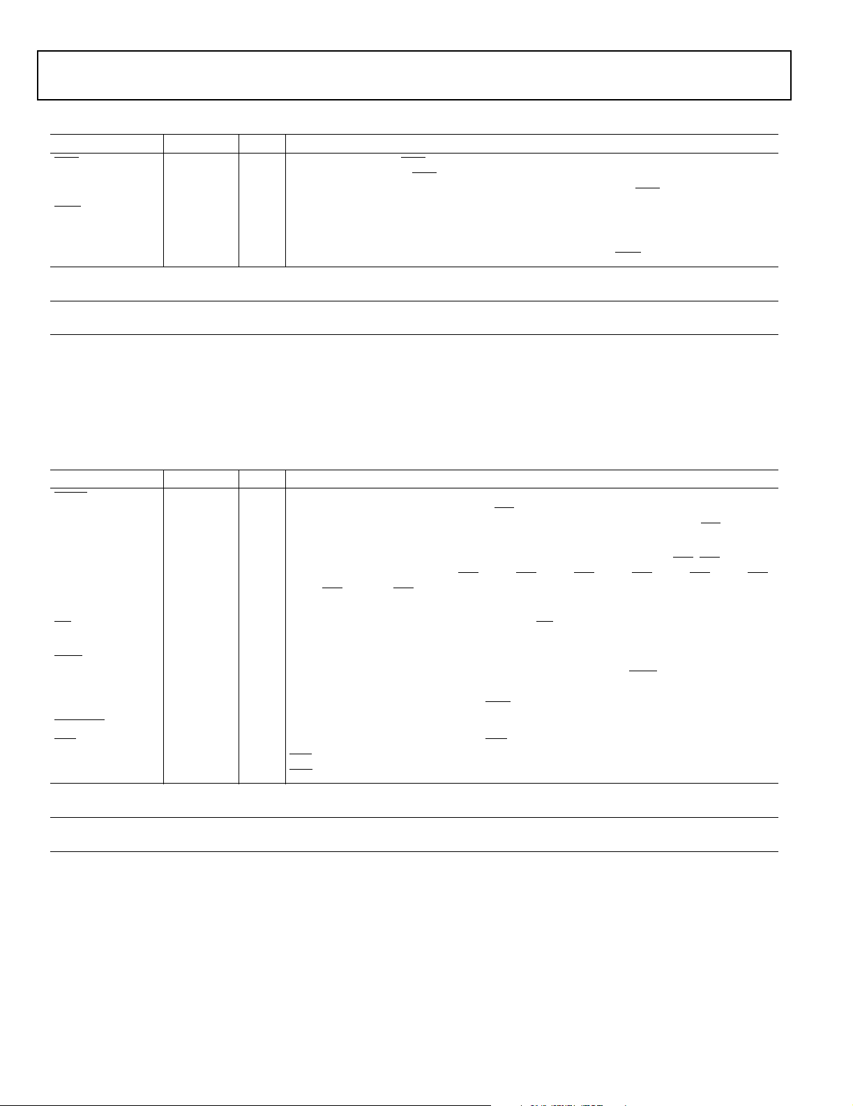
Figure 1. Functional Block Diagram
One Technology Way, P.O.Box 9106, Norwood, MA 02062-9106 U.S.A.
Tel: 781/329-4700 www.analog.com
Fax: 781/326-8703 © 2004 Analog Devices, Inc. All rights reserved.
Page 2

ADSP-TS101S
TABLE OF CONTENTS
General Description ................................................. 3
Dual Compute Blocks ............................................ 4
Data Alignment Buffer (DAB) .................................. 4
Dual Integer ALUs (IALUs) .................................... 4
Program Sequencer ............................................... 5
Interrupt Controller ........................................... 5
Flexible Instruction Set ........................................ 5
On-Chip SRAM Memory ........................................ 5
External Port
(Off-Chip Memory/Peripherals Interface) ................ 6
Host Interface ................................................... 6
Multiprocessor Interface ...................................... 7
SDRAM Controller ............................................ 7
EPROM Interface .............................................. 7
DMA Controller ................................................... 7
Link Ports ........................................................... 8
Timer and General-Purpose I/O ............................... 9
Reset and Booting ................................................. 9
Low Power Operation ............................................ 9
Clock Domains .................................................... 9
Output Pin Drive Strength Control ......................... 10
Power Supplies ................................................... 10
Filtering Reference Voltage and Clocks .................... 10
Development Tools ............................................. 10
Designing an Emulator-
Compatible DSP Board (Target) .......................... 11
Additional Information ........................................ 11
Pin Function Descriptions ....................................... 12
Pin States at Reset ............................................... 12
Pin Definitions ................................................... 12
Strap Pin Function Descriptions ................................ 19
Specifications ........................................................ 20
Recommended Operating Conditions ...................... 20
Electrical Characteristics ....................................... 20
Absolute Maximum Ratings .................................. 21
ESD Sensitivity ................................................... 21
Timing Specifications .......................................... 21
General AC Timing .......................................... 21
Link Ports Data Transfer
and Token Switch Timing ............................... 29
Output Drive Currents ......................................... 32
Test Conditions .................................................. 34
Output Disable Time ......................................... 34
Output Enable Time ......................................... 34
Capacitive Loading ........................................... 34
Environmental Conditions .................................... 36
Thermal Characteristics ..................................... 36
PBGA Pin Configurations ........................................ 36
Outline Dimensions ................................................ 43
Ordering Guide ..................................................... 44
REVISION HISTORY
12/04—Rev. A to Rev. B
Provides more information on clock signals (including a usable
jitter specification) in:
Reference Clocks—Core Clock (CCLK) Cycle Time ..... 22
Reference Clocks—Local Clock (LCLK) Cycle Time .... 22
Reference Clocks—System Clock (SCLK) Cycle Time . . 23
Reference Clocks—Test Clock (TCK) Cycle Time ....... 23
Updates input setup times for external port pins in:
AC Signal Specifications (for SCLK <16.7 ns) ............. 25
Rev. B | Page 2 of 44 | December 2004
Page 3
GENERAL DESCRIPTION
ADSP-TS101S
The ADSP-TS101S TigerSHARC processor is an ultrahigh performance, static superscalar processor optimized for large signal
processing tasks and communications infrastructure. The DSP
combines very wide memory widths with dual computation
blocks—supporting 32- and 40-bit floating-point and 8-, 16-,
32-, and 64-bit fixed-point processing—to set a new standard of
performance for digital signal processors. The TigerSHARC
processor’s static superscalar architecture lets the processor execute up to four instructions each cycle, performing 24 fixedpoint (16-bit) operations or six floating-point operations.
Three independent 128-bit wide internal data buses, each
connecting to one of the three 2M bit memory banks, enable
quad word data, instruction, and I/O accesses and provide
14.4G bytes per second of internal memory bandwidth. Operat-
ing at 300 MHz, the ADSP-TS101S processor’s core has a 3.3 ns
instruction cycle time. Using its Single-Instruction, MultipleData (SIMD) features, the ADSP-TS101S can perform 2.4 billion 40-bit MACs or 600 million 80-bit MACs per second.
Table 1 and Table 2 show the DSP’s performance benchmarks.
Table 1. General-Purpose Algorithm Benchmarks
at 300 MHz
Clock
Benchmark Speed
32-bit algorithm, 600 million MACs/s peak performance
1024 point complex FFT (Radix 2) 32.78 µs 9,835
50-tap FIR on 1024 input 91.67 µs 27,500
Single FIR MAC 1.83 ns 0.55
16-bit algorithm, 2.4 billion MACs/s peak performance
256 point complex FFT (Radix 2) 3.67 µs 1,100
50-tap FIR on 1024 input 24.0 µs 7,200
Single FIR MAC 0.47 ns 0.14
Single complex FIR MAC 1.9 ns 0.57
I/O DMA transfer rate
External port 800M bytes/s n/a
Link ports (each) 250M bytes/s n/a
Cycles
Table 2. 3G Wireless Algorithm Benchmarks
Execution
Benchmark
Turbo decode
384 kbps data channel
Viterbi decode
12.2 kbps AMR
Complex correlation
3.84 Mcps4 with a spreading factor of 256
1
The execution speed is in instruction cycles per second.
2
This value is for six iterations of the algorithm. For eight iterations of the turbo
decoder, this benchmark is 67 MIPS.
3
Adaptive multi rate (AMR)
4
Megachips per second (Mcps)
3
voice channel
1
(MIPS)
51 MIPS
0.86 MIPS
0.27 MIPS
2
The ADSP-TS101S is code compatible with the other
TigerSHARC processors.
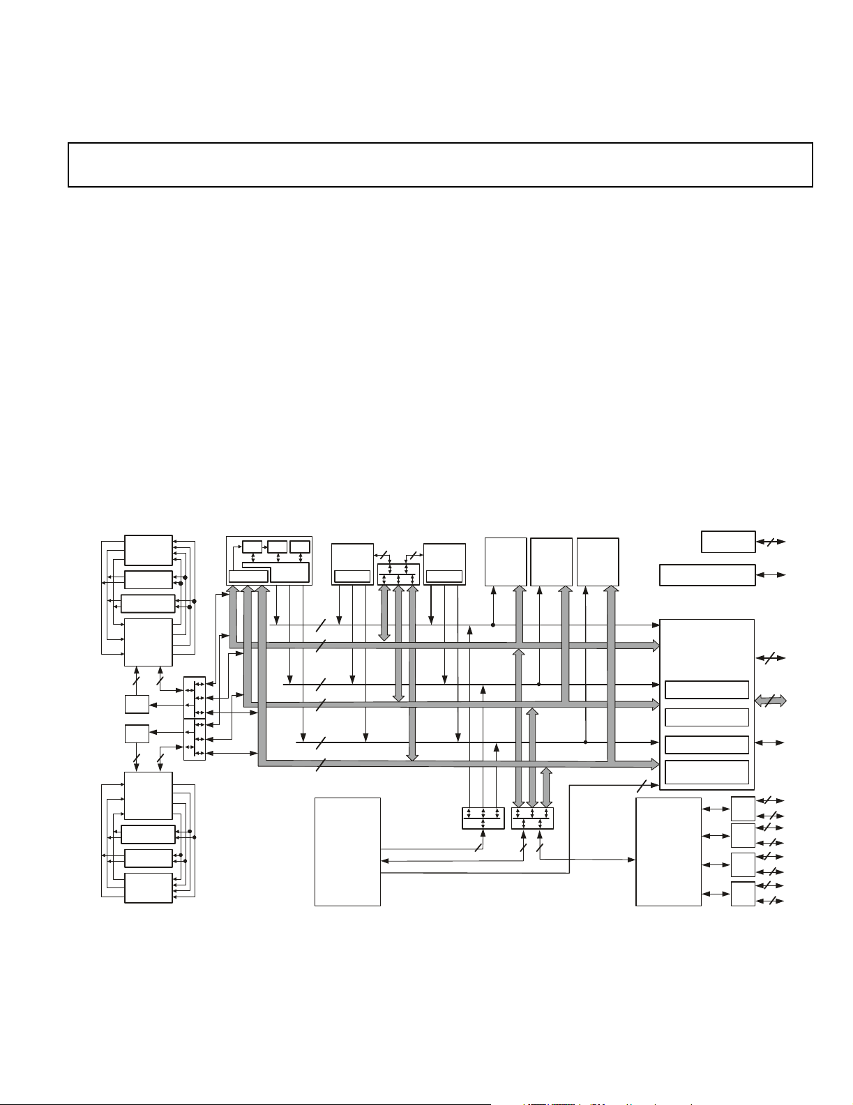
The Functional Block Diagram on Page 1 shows the ADSPTS101S processor’s architectural blocks. These blocks include:
• Dual compute blocks, each consisting of an ALU, multiplier, 64-bit shifter, and 32-word register file and associated
data alignment buffers (DABs)
•Dual integer ALUs (IALUs), each with its own 31-word
register file for data addressing
• A program sequencer with instruction alignment buffer
(IAB), branch target buffer (BTB), and interrupt controller
• Three 128-bit internal data buses, each connecting to one
of three 2M bit memory banks
•On-chip SRAM (6Mbit)
• An external port that provides the interface to host processors, multiprocessing space (DSPs), off-chip memory
mapped peripherals, and external SRAM and SDRAM
• A 14-channel DMA controller
• Four link ports
• Two 64-bit interval timers and timer expired pin
• A 1149.1 IEEE compliant JTAG test access port for on-chip
emulation
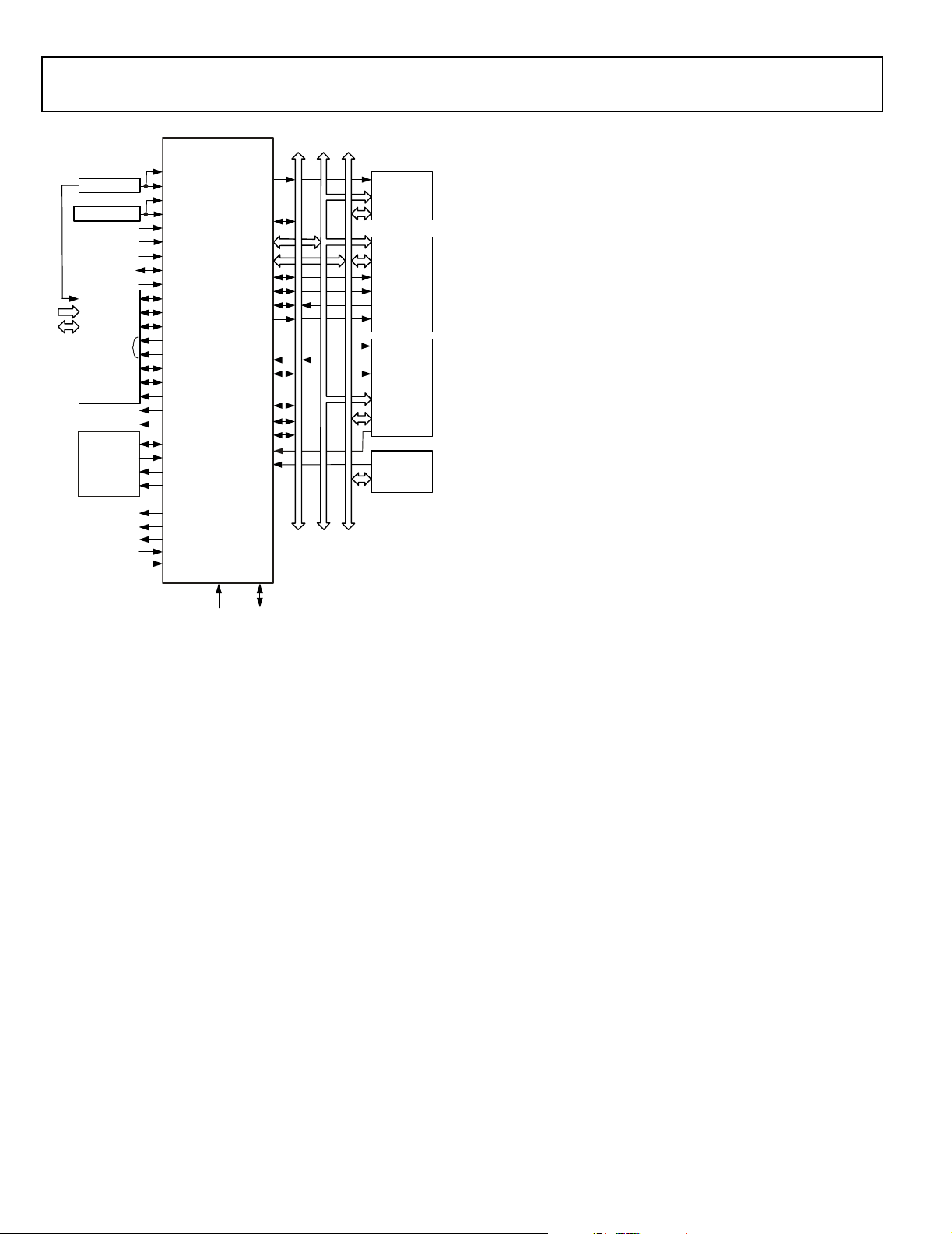
Figure 2 shows a typical single processor system with external
SDRAM. Figure 4 on Page 8 shows a typical multiprocessor
system.
TM
†
The TigerSHARC processor uses a Static Superscalar
architecture. This architecture is superscalar in that the ADSP-TS101S
processor’s core can execute simultaneously from one to four
32-bit instructions encoded in a very large instruction word
(VLIW) instruction line using the DSP’s dual compute blocks.
Because the DSP does not perform instruction reordering at
run-time—the programmer selects which operations will execute in parallel prior to run-time—the order of instructions is
static.
With few exceptions, an instruction line, whether it contains
one, two, three, or four 32-bit instructions, executes with a
throughput of one cycle in an eight-deep processor pipeline.
For optimal DSP program execution, programmers must follow
the DSP’s set of instruction parallelism rules when encoding an
instruction line. In general, the selection of instructions that the
DSP can execute in parallel each cycle depends on the instruction line resources each instruction requires and on the source
and destination registers used in the instructions. The programmer has direct control of three core components—the IALUs,
the compute blocks, and the program sequencer.
The ADSP-TS101S, in most cases, has a two-cycle arithmetic
execution pipeline that is fully interlocked, so whenever a computation result is unavailable for another operation dependent
†
Static Superscalar is a trademark of Analog Devices, Inc.
Rev. B | Page 3 of 44 | December 2004
Page 4
ADSP-TS101S
CLOCK
REFERENCE
SDRAM
MEMORY
(OPTIONAL)
CS
CLK
ADDR
RAS
CAS
DATA
DQM
WE
CKE
A10
LINK
DEVICES
(4 MAX)
(OPTIONAL)
ADSP-TS101S
LCLK_P
SCLK_P
S/LCLK_N
V
REF
LCLKRAT2–0
SCLKFREQ
IRQ3–0
FLAG3–0
ID2–0
MSSD
RAS
CAS
LDQM
HDQM
SDWE
SDCKE
SDA10
FLYBY
IOEN
LXDAT7–0
LXCLKIN
LXCLKOUT
LXDIR
TMR0E
BM
BUSLOCK
CONTROLIMP2–0
DS2–0
ADDR31–0
DATA63–0
WRH/WRL
MS1–0
BR7–0
BOFF
DMAR3–0
RESET JTAG
BMS
BRST
ACK
MSH
HBR
HBG
CPA
DPA
RD
BOOT
EPROM
(OPTIONAL)
CS
ADDR
DATA
MEMORY
(OPTIONAL)
ADDR
DATA
OE
WE
ACK
CS
HOST
PROCESSOR
INTERFACE
(OPTIONAL)
ADDR
DATA
DMA DEVICE
(OPTIONAL)
DATA
registers in the register file individually (word aligned), or
in sets of two (dual aligned) or four (quad aligned).
• ALU—the ALU performs a standard set of arithmetic operations in both fixed- and floating-point formats. It also
performs logic operations.
• Multiplier—the multiplier performs both fixed- and floating-point multiplication and fixed-point multiply and
accumulate.
• Shifter—the 64-bit shifter performs logical and arithmetic
shifts, bit and bit stream manipulation, and field deposit
and extraction operations.
• Accelerator—128-bit unit for trellis decoding (for example,
Viterbi and turbo decoders) and complex correlations for
communication applications.
Using these features, the compute blocks can:
• Provide 8 MACs per cycle peak and 7.1 MACs per cycle
sustained 16-bit performance and provide 2 MACs per
cycle peak and 1.8 MACs per cycle sustained 32-bit performance (based on FIR)
• Execute six single precision floating-point or execute 24
storing intermediate results. Instructions can access the
L
S
A
T
S
O
E
R
T
N
O
C
A
R
D
D
D
A
fixed-point (16-bit) operations per cycle, providing
1,800 MFLOPS or 7.3 GOPS performance
• Perform two complex 16-bit MACs per cycle
• Execute eight trellis butterflies in one cycle
Figure 2. Single Processor System with External SDRAM
on it, the DSP automatically inserts one or more stall cycles as
needed. Efficient programming with dependency-free instructions can eliminate most computational and memory transfer
data dependencies.
In addition, the ADSP-TS101S supports SIMD operations two
ways—SIMD compute blocks and SIMD computations.The
programmer can direct both compute blocks to operate on the
same data (broadcast distribution) or on different data (merged
distribution). In addition, each compute block can execute four
16-bit or eight 8-bit SIMD computations in parallel.
DUAL COMPUTE BLOCKS
The ADSP-TS101S has compute blocks that can execute computations either independently or together as a SIMD engine.
The DSP can issue up to two compute instructions per compute
block each cycle, instructing the ALU, multiplier, or shifter to
perform independent, simultaneous operations.
The compute blocks are referred to as X and Y in assembly syntax, and each block contains three computational units—an
ALU, a multiplier, a 64-bit shifter—and a 32-word register file.
• Register file—each compute block has a multiported
32-word, fully orthogonal register file used for transferring
data between the computation units and data buses and for
DATA ALIGNMENT BUFFER (DAB)
The DAB is a quad word FIFO that enables loading of quad
word data from nonaligned addresses. Normally, load instructions must be aligned to their data size so that quad words are
loaded from a quad aligned address. Using the DAB significantly improves the efficiency of some applications, such as FIR
filters.
DUAL INTEGER ALUS (IALUS)
The ADSP-TS101S has two IALUs that provide powerful
address generation capabilities and perform many general-purpose integer operations. Each of the IALUs:
• Provides memory addresses for data and update pointers
• Supports circular buffering and bit-reverse addressing
• Performs general-purpose integer operations, increasing
programming flexibility
• Includes a 31-word register file for each IALU
As address generators, the IALUs perform immediate or indirect (pre- and post-modify) addressing. They perform modulus
and bit-reverse operations with no constraints placed on memory addresses for the modulus data buffer placement. Each
IALU can specify either a single, dual, or quad word access from
memory.
The IALUs have hardware support for circular buffers, bit
reverse, and zero-overhead looping. Circular buffers facilitate
efficient programming of delay lines and other data structures
required in digital signal processing, and they are commonly
Rev. B | Page 4 of 44 | December 2004
Page 5

ADSP-TS101S
used in digital filters and Fourier transforms. Each IALU provides registers for four circular buffers, so applications can set
up a total of eight circular buffers. The IALUs handle address
pointer wraparound automatically, reducing overhead, increasing performance, and simplifying implementation. Circular
buffers can start and end at any memory location.
Because the IALU’s computational pipeline is one cycle deep, in
most cases, integer results are available in the next cycle. Hardware (register dependency check) causes a stall if a result is
unavailable in a given cycle.
PROGRAM SEQUENCER
The ADSP-TS101S processor’s program sequencer supports:
• A fully interruptible programming model with flexible programming in assembly and C/C++ languages; handles
hardware interrupts with high throughput and no aborted
instruction cycles.
• An eight-cycle instruction pipeline—three-cycle fetch pipe
and five-cycle execution pipe—with computation results
available two cycles after operands are available.
• The supply of instruction fetch memory addresses; the
sequencer’s instruction alignment buffer (IAB) caches up
to five fetched instruction lines waiting to execute; the program sequencer extracts an instruction line from the IAB
and distributes it to the appropriate core component for
execution.
• The management of program structures and determination
of program flow according to JUMP, CALL, RTI, RTS
instructions, loop structures, conditions, interrupts, and
software exceptions.
• Branch prediction and a 128-entry branch target buffer
(BTB) to reduce branch delays for efficient execution of
conditional and unconditional branch instructions and
zero-overhead looping; correctly predicted branches that
are taken occur with zero-to-two overhead cycles, overcoming the three-to-six stage branch penalty.
• Compact code without the requirement to align code in
memory; the IAB handles alignment.
Interrupt Controller
The DSP supports nested and non-nested interrupts. Each
interrupt type has a register in the interrupt vector table. Also,
each has a bit in both the interrupt latch register and the interrupt mask register. All interrupts are fixed as either level
sensitive or edge sensitive, except the IRQ3–0
rupts, which are programmable.
The DSP distinguishes between hardware interrupts and software exceptions, handling them differently. When a software
exception occurs, the DSP aborts all other instructions in the
instruction pipe. When a hardware interrupt occurs, the DSP
continues to execute instructions already in the instruction pipe.
hardware inter-
Flexible Instruction Set
The 128-bit instruction line, which can contain up to four 32-bit
instructions, accommodates a variety of parallel operations for
concise programming. For example, one instruction line can
direct the DSP to conditionally execute a multiply, an add, and a
subtract in both computation blocks while it also branches to
another location in the program. Some key features of the
instruction set include:
• Enhanced instructions for communications infrastructure
to govern trellis decoding (for example, Viterbi and turbo
decoders) and despreading via complex correlations
• Algebraic assembly language syntax
• Direct support for all DSP, imaging, and video arithmetic
types, eliminating hardware modes
• Branch prediction encoded in instruction, enables zerooverhead loops
• Parallelism encoded in instruction line
• Conditional execution optional for all instructions
• User-defined, programmable partitioning between program and data memory
ON-CHIP SRAM MEMORY
The ADSP-TS101S has 6M bits of on-chip SRAM memory,
divided into three blocks of 2M bits (64K words × 32 bits). Each
block—M0, M1, and M2—can store program, data, or both, so
applications can configure memory to suit specific needs. Placing program instructions and data in different memory blocks,
however, enables the DSP to access data while performing an
instruction fetch.
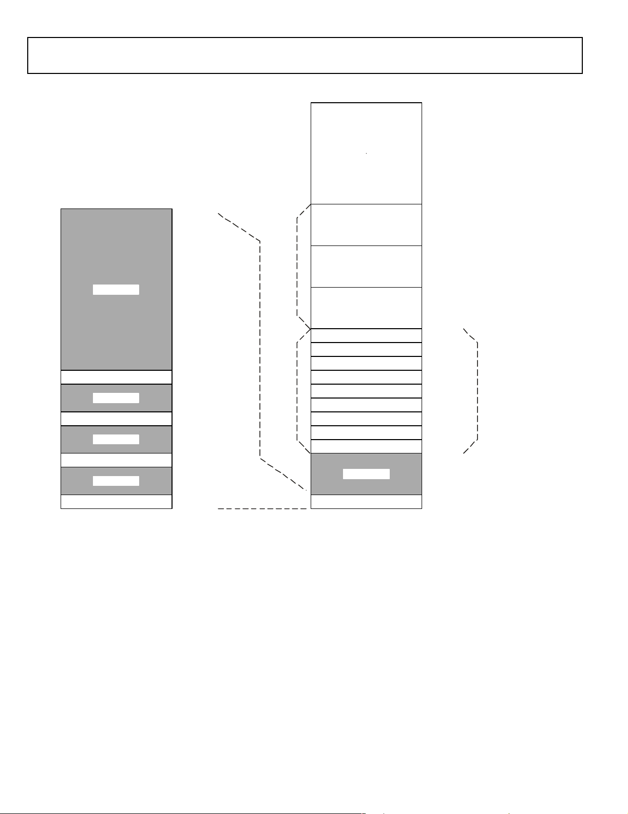
The DSP’s internal and external memory (Figure 3) is organized
into a unified memory map, which defines the location
(address) of all elements in the system.
The memory map is divided into four memory areas—host
space, external memory, multiprocessor space, and internal
memory—and each memory space, except host memory, is subdivided into smaller memory spaces.
Each internal memory block connects to one of the 128-bit wide
internal buses—block M0 to bus MD0, block M1 to bus MD1,
and block M2 to bus MD2—enabling the DSP to perform three
memory transfers in the same cycle. The DSP’s internal bus
architecture provides a total memory bandwidth of 14.4G bytes
per second, enabling the core and I/O to access eight 32-bit data
words (256 bits) and four 32-bit instructions each cycle. The
DSP’s flexible memory structure enables:
• DSP core and I/O access of different memory blocks in the
same cycle
• DSP core access of all three memory blocks in parallel—
one instruction and two data accesses
• Programmable partitioning of program and data memory
• Program access of all memory as 32-, 64-, or 128-bit
words—16-bit words with the DAB
• Complete context switch in less than 20 cycles (66 ns)
Rev. B | Page 5 of 44 | December 2004
Page 6
ADSP-TS101S
INTERNAL SPACE
RE SER VE D
INTERNAL REGISTERS (UREGS)
RE SER VE D
INTERNAL MEMORY 2
RE SER VE D
INTERNAL MEMORY 1
RE SE RV E D
INTERNAL MEMORY 0
0x 003FF FFF
0x00300000
0x00280000
0x00200000
0x 00180 7FF
0x00180000
0x0010FFFF
0x00100000
0x0008FFFF
0x00080000
0x0000FFFF
0x00000000
GLOBAL SPACE
HOST
(MSH)
E
C
A
P
S
Y
R
O
M
E
M
L
A
N
R
E
T
X
E
E
C
A
P
S
Y
R
O
M
E
M
R
O
S
S
E
C
O
R
P
I
T
L
U
M
BANK 1
(MS1)
BANK 0
(MS0)
SDRAM
(MSSD)
PROC ESSOR I D 7
PROC ESSOR I D 6
PROC ESSOR I D 5
PROC ESSOR I D 4
PROC ESSOR I D 3
PROC ESSOR I D 2
PROC ESSOR I D 1
PROC ESSOR I D 0
BROADCAST
RESERVED
INTER NAL ME MORY
0xFFFFFFFF
0 x100 00000
0 x0C 0000 00
0 x080 00000
0 x040 00000
0 x03C 000 00
0 x038 00000
0 x034 00000
0 x030 00000
0 x02C 000 00
0 x028 00000
0 x024 00000
0 x020 00000
0 x01C 000 00
0x003FFFFF
0 x000 00000
EACH IS A COPY
OF INTERNAL SPACE
Figure 3. Memory Map
EXTERNAL PORT (OFF-CHIP MEMORY/PERIPHERALS INTERFACE)
The ADSP-TS101S processor’s external port provides the processor’s interface to off-chip memory and peripherals. The
4G word address space is included in the DSP’s unified address
space. The separate on-chip buses—three 128-bit data buses and
three 32-bit address buses—are multiplexed at the external port
to create an external system bus with a single 64-bit data bus
and a single 32-bit address bus. The external port supports data
transfer rates of 800M bytes per second over external bus.
The external bus can be configured for 32- or 64-bit operation.
When the system bus is configured for 64-bit operation, the
lower 32 bits of the external data bus connect to even addresses,
and the upper 32 bits connect to odd addresses.
Rev. B | Page 6 of 44 | December 2004
The external port supports pipelined, slow, and SDRAM protocols. Addressing of external memory devices and memory
mapped peripherals is facilitated by on-chip decoding of high
order address lines to generate memory bank select signals.
The ADSP-TS101S provides programmable memory, pipeline
depth, and idle cycle for synchronous accesses, and external
acknowledge controls to support interfacing to pipelined or
slow devices, host processors, and other memory-mapped
peripherals with variable access, hold, and disable time
requirements.
Host Interface
The ADSP-TS101S provides an easy and configurable interface
between its external bus and host processors through the external port. To accommodate a variety of host processors, the host
Page 7

ADSP-TS101S
interface supports pipelined or slow protocols for accesses of the
host as slave. Each protocol has programmable transmission
parameters, such as idle cycles, pipe depth, and internal
wait cycles.
The host interface supports burst transactions initiated by a host
processor. After the host issues the starting address of the burst
and asserts the BRST
internally while the host continues to assert BRST
The host interface provides a deadlock recovery mechanism that
enables a host to recover from deadlock situations involving the
DSP. The BOFF
nism. When the host asserts BOFF
current transaction and asserts HBG
nal bus.
The host can directly read or write the internal memory of the
ADSP-TS101S, and it can access most of the DSP registers,
including DMA control (TCB) registers. Vector interrupts support efficient execution of host commands.
signal, the DSP increments the address
.
signal provides the deadlock recovery mecha-
, the DSP backs off the
and relinquishes the exter-
Multiprocessor Interface
The ADSP-TS101S offers powerful features tailored to multiprocessing DSP systems through the external port and link
ports. This multiprocessing capability provides highest bandwidth for interprocessor communication, including:
• Up to eight DSPs on a common bus
• On-chip arbitration for glueless multiprocessing
• Link ports for point-to-point communication
The external port and link ports provide integrated, glueless
multiprocessing support.
The external port supports a unified address space (see Figure 3)
that enables direct interprocessor accesses of each ADSPTS101S processor’s internal memory and registers. The DSP’s
on-chip distributed bus arbitration logic provides simple, glueless connection for systems containing up to eight ADSPTS101S processors and a host processor. Bus arbitration has a
rotating priority. Bus lock supports indivisible read-modifywrite sequences for semaphores. A bus fairness feature prevents
one DSP from holding the external bus too long.
The DSP’s four link ports provide a second path for interprocessor communications with throughput of 1G bytes per second.
The cluster bus provides 800M bytes per second throughput—
with a total of 1.8G bytes per second interprocessor bandwidth.
SDRAM Controller
The SDRAM controller controls the ADSP-TS101S processor’s
transfers of data to and from synchronous DRAM (SDRAM).
The throughput is 32 or 64 bits per SCLK cycle using the external port and SDRAM control pins.
The SDRAM interface provides a glueless interface with standard SDRAMs—16M bit, 64M bit, 128M bit, and 256M bit. The
DSP directly supports a maximum of 64M words × 32 bits of
SDRAM. The SDRAM interface is mapped in external memory
in the DSP’s unified memory map.
EPROM Interface
The ADSP-TS101S can be configured to boot from external
8-bit EPROM at reset through the external port. An automatic
process (which follows reset) loads a program from the EPROM
into internal memory. This process uses 16 wait cycles for each
read access. During booting, the BMS
EPROM chip select signal. The EPROM boot procedure uses
DMA Channel 0, which packs the bytes into 32-bit instructions.
Applications can also access the EPROM (write flash memories)
during normal operation through DMA.
The EPROM or flash memory interface is not mapped in the
DSP’s unified memory map. It is a byte address space limited to
a maximum of 16M bytes (24 address bits). The EPROM or
flash memory interface can be used after boot via a DMA.
pin functions as the
DMA CONTROLLER
The ADSP-TS101S processor’s on-chip DMA controller, with
14 DMA channels, provides zero-overhead data transfers without processor intervention. The DMA controller operates
independently and invisibly to the DSP’s core, enabling DMA
operations to occur while the DSP’s core continues to execute
program instructions. The DMA controller performs DMA
transfers between:
• Internal memory and external memory and memorymapped peripherals
• Internal memory of other DSPs on a common bus, a host
processor, or link port I/O
• External memory and external peripherals or link port I/O
• External bus master and internal memory or link port I/O
The DMA controller provides a number of additional features.
The DMA controller supports flyby transfers. Flyby operations
only occur through the external port (DMA Channel 0) and do
not involve the DSP’s core. The DMA controller acts as a conduit to transfer data from one external device to another
through external memory. During a transaction, the DSP:
• Relinquishes the external data bus
• Outputs addresses, memory selects (MS1–0
, and SDWE) and the FLYBY, IOEN, and RD/WR
CAS
strobes
•Responds to ACK
DMA chaining is also supported by the DMA controller. DMA
chaining operations enable applications to automatically link
one DMA transfer sequence to another for continuous transmission. The sequences can occur over different DMA channels
and have different transmission attributes.
The DMA controller also supports two-dimensional transfers.
The DMA controller can access and transfer two-dimensional
memory arrays on any DMA transmit or receive channel. These
transfers are implemented with index, count, and modify registers for both the X and Y dimensions.
, MSSD, RAS,
Rev. B | Page 7 of 44 | December 2004
Page 8
ADSP-TS101S
001
000
RESET
CLOCK
REFERENCE
VOLTAGE
LINK
DEVICES
(4 MAX)
(OPTIONAL)
ID2–0
RESET
CLKS/REFS
ID2–0
RESET
CLKS/REFS
SCLK_P
LCLK_P
S/LCLK_N
V
REF
LCLKRAT2–0
SCLKFREQ
IRQ3–0
FLAG3–0
LINK
LXDAT7–0
LXCLKIN
LXCLKOUT
LXDIR
TMR0E
BM
CONTROLIMP2–0
DS2–0
ADSP-TS101 #7
ADSP-TS101 #6
ADSP-TS101 #5
ADSP-TS101 #4
ADSP-TS101 #3
ADSP-TS101 #2
ADSP-TS101 #1
ADDR31–0
DATA63–0
CONTROL
LINK
ADSP-TS101 #0
ADDR31–0
DATA63–0
BUSLOCK
DMAR3–0
CONTROL
BR7–2,0
BR1
BR7–1
BR0
RD
WRH/L
ACK
MS1–0
BMS
CPA
DPA
BOFF
BRST
HBR
HBG
MSH
FLYBY
IOEN
MSSD
RAS
CAS
LDQM
HDQM
SDWE
SDCKE
SDA10
L
S
S
O
R
T
N
O
C
L
O
R
T
N
O
C
A
E
T
R
A
D
D
D
A
S
S
A
E
T
R
A
D
D
D
A
ADDR
DATA
OE
WE
ACK
CS
CS
ADDR
DATA
ADDR
DATA
CS
RAS
CAS
DQM
WE
CKE
A10
ADDR
DATA
GLOBAL
MEMORY
AND
PERIPHERALS
(OPTIONAL)
BOOT
EPROM
(OPTIONAL)
CLOCK
HOST
PROCESSOR
INTERFACE
(OPTIONAL)
SDRAM
MEMORY
(OPTIONAL)
CLK
Figure 4. Shared Memory Multiprocessing System
The DMA controller performs the following DMA operations:
• External port block transfers. Four dedicated bidirectional
DMA channels transfer blocks of data between the DSP’s
internal memory and any external memory or memorymapped peripheral on the external bus. These transfers
support master mode and handshake mode protocols.
• Link port transfers. Eight dedicated DMA channels (four
transmit and four receive) transfer quad word data only
between link ports and between a link port and internal or
Rev. B | Page 8 of 44 | December 2004
external memory. These transfers only use handshake
mode protocol. DMA priority rotates between the four
receive channels.
• AutoDMA transfers. Two dedicated unidirectional DMA
channels transfer data received from an external bus master
to internal memory or to link port I/O. These transfers only
use slave mode protocol, and an external bus master must
initiate the transfer.
LINK PORTS
The DSP’s four link ports provide additional 8-bit bidirectional
I/O capability. With the ability to operate at a double data rate—
latching data on both the rising and falling edges of the clock—
Page 9
ADSP-TS101S
running at 125 MHz, each link port can support up to
250M bytes per second, for a combined maximum throughput
of 1G bytes per second.
The link ports provide an optional communications channel
that is useful in multiprocessor systems for implementing point
to point interprocessor communications. Applications can also
use the link ports for booting.
Each link port has its own double-buffered input and output
registers. The DSP’s core can write directly to a link port’s transmit register and read from a receive register, or the DMA
controller can perform DMA transfers through eight (four
transmit and four receive) dedicated link port DMA channels.
Each link port has three signals that control its operation.
LxCLKOUT and LxCLKIN implement clock/acknowledge
handshaking. LxDIR indicates the direction of transfer and is
used only when buffering the LxDAT signals. An example application would be using differential low-swing buffers for long
twisted-pair wires. LxDAT provides the 8-bit data bus
input/output.
Applications can program separate error detection mechanisms
for transmit and receive operations (applications can use the
checksum mechanism to implement consecutive link port
transfers), the size of data packets, and the speed at which bytes
are transmitted.
Under certain conditions, the link port receiver can initiate a
token switch to reverse the direction of transfer; the transmitter
becomes the receiver and vice versa.
TIMER AND GENERAL-PURPOSE I/O
The ADSP-TS101S has a timer pin (TMR0E) that generates output when a programmed timer counter has expired. Also, the
DSP has four programmable general-purpose I/O pins
(FLAG3–0) that can function as either single bit input or output. As outputs, these pins can signal peripheral devices; as
inputs, they can provide the test for conditional branching.
RESET AND BOOTING
The ADSP-TS101S has two levels of reset (see reset specifications on Page 24):
• Power-up reset—after power-up of the system, and strap
options are stable, the RESET
• Normal reset—for any resets following the power-up reset
sequence, the RESET
pin must be asserted.
The DSP can be reset internally (core reset) by setting the
SWRST bit in SQCTL. The core is reset, but not the external
port or I/O.
pin must be asserted (low).
After reset, the ADSP-TS101S has four boot options for beginning operation:
• Boot from EPROM. The DSP defaults to EPROM booting
when the BMS
pin strap option is set low. See Strap Pin
Function Descriptions on Page 19.
• Boot by an external master (host or another ADSPTS101S). Any master on the cluster bus can boot the
ADSP-TS101S through writes to its internal memory or
through autoDMA.
• Boot by link port. All four receive link DMA channels are
initialized after reset to transfer a 256-word block to internal memory address 0 to 255, and to issue an interrupt at
the end of the block (similar to EP DMA). The corresponding DMA interrupts are set to address zero (0).
• No boot—Start running from an external memory. Using
the “no boot” option, the ADSP-TS101S must start running
from an external memory, caused by asserting one of the
IRQ3–0
interrupt signals.
The ADSP-TS101S core always exits from reset in the idle state
and waits for an interrupt. Some of the interrupts in the interrupt vector table are initialized and enabled after reset.
LOW POWER OPERATION
The ADSP-TS101S can enter a low power sleep mode in which
its core does not execute instructions, reducing power consumption to a minimum. The ADSP-TS101S exits sleep mode
when it senses a falling edge on any of its IRQ3–0
interrupt
inputs. The interrupt, if enabled, causes the ADSP-TS101S to
execute the corresponding interrupt service routine. This feature is useful for systems that require a low power standby
mode.
CLOCK DOMAINS
As shown in Figure 5, the ADSP-TS101S has two clock inputs,
SCLK (system clock) and LCLK (local clock).
SCLK_P
LCLK_P
LCLKRATx
LCTLx REGISTER
DLL
DLL
PLL
DLL
SPD BITS,
Figure 5. Clock Domains
/LR
DLL
These inputs drive its two major clock domains:
• SCLK (system clock). Provides clock input for the external
bus interface and defines the ac specification reference for
the external bus signals. The external bus interface runs at
1× the SCLK frequency. A DLL locks internal SCLK to
SCLK input.
• LCLK (local clock). Provides clock input to the internal
clock driver, CCLK, which is the internal clock for the core,
internal buses, memory, and link ports. The instruction
EXTERNAL INTERFACE
CCLK
(INSTRUCTION RATE)
LxCLKOUT/LxCLKIN
(LINK PORT RATE)
Rev. B | Page 9 of 44 | December 2004
Page 10
ADSP-TS101S
execution rate is equal to CCLK. A PLL from LCLK generates CCLK which is phase-locked. The LCLKRAT pins
define the clock multiplication of LCLK to CCLK (see
Table 4). The link port clock is generated from CCLK via a
software programmable divisor. RESET
must be asserted
until LCLK is stable and within specification for at least
2 ms. This applies to power-up as well as any dynamic
modification of LCLK after power-up. Dynamic modification may include LCLK going out of specification as long as
RESET
is asserted.
Connecting SCLK and LCLK to the same clock source is a
requirement for the device. Using an integer clock multiplication value provides predictable cycle-by-cycle operation, a
requirement of fault-tolerant systems and some multiprocessing systems.
Noninteger values are completely functional and acceptable for
applications that do not require predictable cycle-by-cycle
operation.
OUTPUT PIN DRIVE STRENGTH CONTROL
Pins CONTROLIMP2-0 and DS2-0 work together to control
the output drive strength of two groups of pins, the
Address/Data/Control pin group and the Link pin group.
CONTROLIMP2-0 independently configures the two pin
groups to the maximum drive strength or to a digitally controlled drive strength that is selectable by the DS2-0 pins (see
Table 13 on Page 18). If the digitally controlled drive strength is
selected for a pin group, the DS2-0 pins determine one of eight
strength levels for that group (see Table 14 on Page 18). The
drive strength selected varies the slew rate of the driver. Drive
strength 0 (DS2-0 = 000) is the weakest and slowest slew rate.
Drive strength 7 (DS2-0 = 111) is the strongest and fastest slew
rate.
The stronger drive strengths are useful for high frequency
switching while the lower strengths may allow use of a relaxed
design methodology. The strongest drive strengths have a larger
di/dt and thus require more attention to signal integrity issues
such a ringing, reflections and coupling. Also a larger di/dt can
increase external supply rail noise, which impacts power supply
and power distribution design.
The drive strengths for the EMU
, CPA, and DPA pins are not
controllable and are fixed to the maximum level.
For drive strength calculation, see Output Drive Currents on
Page 32.
POWER SUPPLIES
The ADSP-TS101S has separate power supply connections for
internal logic (V
) power supply. The internal (VDD) and analog (V
(V
DD_IO
supplies must meet the 1.2 V requirement. The I/O buffer
(V
) supply must meet the 3.3 V requirement.
DD_IO
The analog supply (V
produce a stable clock, systems must provide a clean power supply to power input V
bypassing the V
), analog circuits (V
DD
) powers the clock generator PLLs. To
DD_A
. Designs must pay critical attention to
DD_A
supply.
DD_A
), and I/O buffer
DD_A
DD_A
)
The required power-on sequence for the DSP is to provide V
(and V
) before V
DD_A
DD_IO
.
DD
FILTERING REFERENCE VOLTAGE AND CLOCKS
Figure 6 shows a possible circuit for filtering V
LCLK_N. This circuit provides the reference voltage for the
switching voltage, system clock, and local clock references.
V
DD_IO
R1
R2 C1 C2
V
SS
R1: 2k⍀ SERIES RESISTOR
R2: 1.67k⍀ SERIES RESIST OR
C1: 1F CAPACITOR (SMD)
C2: 1nF CAPACITOR (HF SMD) PLACED CLOSE TO DSP’S PINS
Figure 6. V
, SCLK_N, and LCLK_N Filter
REF
, SCLK_N, and
REF
V
REF
SCLK_N
LCLK_N
DEVELOPMENT TOOLS
The ADSP-TS101S is supported with a complete set of
CROSSCORE
including Analog Devices emulators and VisualDSP++
opment environment. The same emulator hardware that
supports other TigerSHARC processors also fully emulates the
ADSP-TS101S.
The VisualDSP++ project management environment lets programmers develop and debug an application. This environment
includes an easy to use assembler (which is based on an algebraic syntax), an archiver (librarian/library builder), a linker, a
loader, a cycle-accurate instruction-level simulator, a C/C++
compiler, and a C/C++ run-time library that includes DSP and
mathematical functions. A key point for these tools is C/C++
code efficiency. The compiler has been developed for efficient
translation of C/C++ code to DSP assembly. The DSP has architectural features that improve the efficiency of compiled C/C++
code.
The VisualDSP++ debugger has a number of important features. Data visualization is enhanced by a plotting package that
offers a significant level of flexibility. This graphical representation of user data enables the programmer to quickly determine
the performance of an algorithm. As algorithms grow in complexity, this capability can have increasing significance on the
designer’s development schedule, increasing productivity. Statistical profiling enables the programmer to nonintrusively poll
the processor as it is running the program. This feature, unique
to VisualDSP++, enables the software developer to passively
gather important code execution metrics without interrupting
the real-time characteristics of the program. Essentially, the
developer can identify bottlenecks in software quickly and
†
CROSSCORE is a registered trademark of Analog Devices, Inc.
‡
VisualDSP++ is a registered trademark of Analog Devices, Inc.
®
†
software and hardware development tools,
®
‡
devel-
Rev. B | Page 10 of 44 | December 2004
Page 11

ADSP-TS101S
efficiently. By using the profiler, the programmer can focus on
those areas in the program that impact performance and take
corrective action.
Debugging both C/C++ and assembly programs with the
VisualDSP++ debugger, programmers can:
• View mixed C/C++ and assembly code (interleaved source
and object information)
• Insert breakpoints
• Set conditional breakpoints on registers, memory,
and stacks
• Trace instruction execution
• Perform linear or statistical profiling of program execution
• Fill, dump, and graphically plot the contents of memory
• Perform source level debugging
• Create custom debugger windows
The VisualDSP++ IDDE lets programmers define and manage
DSP software development. Its dialog boxes and property pages
let programmers configure and manage all of the TigerSHARC
development tools, including the color syntax highlighting in
the VisualDSP++ editor. This capability permits programmers
to:
• Control how the development tools process inputs and
generate outputs
• Maintain a one-to-one correspondence with the tool’s
command line switches
The VisualDSP++ Kernel (VDK) incorporates scheduling and
resource management tailored specifically to address the memory and timing constraints of DSP programming. These
capabilities enable engineers to develop code more effectively,
eliminating the need to start from the very beginning, when
developing new application code. The VDK features include
threads, critical and unscheduled regions, semaphores, events,
and device flags. The VDK also supports priority-based, preemptive, cooperative, and time-sliced scheduling approaches. In
addition, the VDK was designed to be scalable. If the application
does not use a specific feature, the support code for that feature
is excluded from the target system.
Because the VDK is a library, a developer can decide whether to
use it or not. The VDK is integrated into the VisualDSP++
development environment, but can also be used via standard
command line tools. When the VDK is used, the development
environment assists the developer with many error-prone tasks
and assists in managing system resources, automating the generation of various VDK-based objects, and visualizing the
system state, when debugging an application that uses the VDK.
VCSE is Analog Devices technology for creating, using, and
reusing software components (independent modules of substantial functionality) to quickly and reliably assemble software
applications. It is also used for downloading components from
the Web, dropping them into the application, and publishing
component archives from within VisualDSP++. VCSE supports
component implementation in C/C++ or assembly language.
Use the expert linker to visually manipulate the placement of
code and data on the embedded system. View memory utilization in a color-coded graphical form, easily move code and data
to different areas of the DSP or external memory with a drag of
the mouse, examine run-time stack and heap usage. The expert
linker is fully compatible with existing linker definition file
(LDF), allowing the developer to move between the graphical
and textual environments.
Analog Devices DSP emulators use the IEEE 1149.1 JTAG Test
Access Port of the ADSP-TS101S processor to monitor and control the target board processor during emulation. The emulator
provides full speed emulation, allowing inspection and modification of memory, registers, and processor stacks. Nonintrusive
in-circuit emulation is assured by the use of the processor’s
JTAG interface—the emulator does not affect target system
loading or timing.
In addition to the software and hardware development tools
available from Analog Devices, third parties provide a wide
range of tools supporting the TigerSHARC processor family.
Hardware tools include TigerSHARC processor PC plug-in
cards. Third party software tools include DSP libraries, realtime operating systems, and block diagram design tools.
DESIGNING AN EMULATORCOMPATIBLE DSP BOARD (TARGET)
The Analog Devices family of emulators are tools that every
DSP developer needs to test and debug hardware and software
systems. Analog Devices has supplied an IEEE 1149.1 JTAG test
access port (TAP) on each JTAG DSP. The emulator uses the
TAP to access the internal features of the DSP, allowing the
developer to load code, set breakpoints, observe variables,
observe memory, and examine registers. The DSP must be
halted to send data and commands, but once an operation has
been completed by the emulator, the DSP system is set running
at full speed with no impact on system timing.
To use these emulators, the target board must include a header
that connects the DSP’s JTAG port to the emulator.
For details on target board design issues including mechanical
layout, single processor connections, multiprocessor scan
chains, signal buffering, signal termination, and emulator pod
logic, see the EE-68: Analog Devices JTAG Emulation Technical
Reference on the Analog Devices website (www.analog.com)—
use site search on “EE-68.” This document is updated regularly
to keep pace with improvements to emulator support.
ADDITIONAL INFORMATION
This data sheet provides a general overview of the ADSPTS101S processor’s architecture and functionality. For detailed
information on the ADSP-TS101S processor’s core architecture
and instruction set, see the ADSP-TS101 TigerSHARC Processor
Programming Reference and the ADSP-TS101 TigerSHARC Processor Hardware Reference. For detailed information on the
development tools for this processor, see the VisualDSP++
User’s Guide for TigerSHARC Processors.
Rev. B | Page 11 of 44 | December 2004
Page 12
ADSP-TS101S
PIN FUNCTION DESCRIPTIONS
While most of the ADSP-TS101S processor’s input pins are normally synchronous—tied to a specific clock—a few are
asynchronous. For these asynchronous signals, an on-chip synchronization circuit prevents metastability problems. The
synchronous ac specification for asynchronous signals is used
only when predictable cycle-by-cycle behavior is required.
All inputs are sampled by a clock reference, therefore input
PIN STATES AT RESET
The output pins can be three-stated during normal operation.
The DSP three-states all outputs during reset, allowing these
pins to get to their internal pull-up or pull-down state. Some
output pins (control signals) have a pull-up or pull-down that
maintains a known value during transitions between different
drivers.
specifications (asynchronous minimum pulse widths or synchronous input setup and hold) must be met to guarantee
recognition.
PIN DEFINITIONS
The Type column in the following pin definitions tables
describes the pin type, when the pin is used in the system. The
Term (for termination) column describes the pin termination
type if the pin is not used by the system. Note that some pins are
always used (indicated with au symbol).
Table 3. Pin Definitions—Clocks and Reset
Signal Type Term Description
LCLK_N I au Local Clock Reference. Connect this pin to V
as shown in Figure 6.
REF
LCLK_P I au Local Clock Input. DSP clock input. The instruction cycle rate = n × LCLK, where n is user-
programmable to 2, 2.5, 3, 3.5, 4, 5, or 6. For more information, see Clock Domains on Page 9.
LCLKRAT2–0
1
I (pd2) au LCLK Ratio. The DSP’s core clock (instruction cycle rate) = n × LCLK, where n is user-program-
mable to 2, 2.5, 3, 3.5, 4, 5, or 6 as shown in Table 4. These pins must have a constant value while
the DSP is powered.
SCLK_N I au System Clock Reference. Connect this pin to V
as shown in Figure 6.
REF
SCLK_P I au System Clock Input. The DSP’s system input clock for cluster bus. This pin must be connected
to the same clock source as LCLK_P. For more information, see Clock Domains on Page 9.
SCLKFREQ
3
I (pu2) au SCLK Frequency. SCLKFREQ = 1 is required. The SCLKFREQ pin must have a constant value while
the DSP is powered.
RESET
I/A au Reset. Sets the DSP to a known state and causes program to be in idle state. RESET must be
asserted at specified time according to the type of reset operation. For details, see Reset and
Booting on Page 9.
Type column symbols: A = asynchronous; G = ground; I = input; O = output; o/d = open drain output; P = power supply;
pd = internal pull-down approximately 100 k
Term (for termination) column symbols: epd = external pull-down approximately 10 k
, nc = not connected; au = always used.
to V
DD-IO
1
The internal pull-down may not be sufficient. A stronger pull-down may be necessary.
2
See Electrical Characteristics on Page 20 for maximum and minimum current consumption for pull-up and pull-down resistances.
3
The internal pull-up may not be sufficient. A stronger pull-up may be necessary.
Ω; pu = internal pull-up approximately 100 kΩ; T = three-state
Ω to V
; epu = external pull-up approximately 10 kΩ
SS
Table 4. LCLK Ratio
LCLKRAT2–0 Ratio
000 (default) 2
001 2.5
010 3
011 3.5
100 4
101 5
110 6
111 Reserved
Rev. B | Page 12 of 44 | December 2004
Page 13

Table 5. Pin Definitions—External Port Bus Controls
ADSP-TS101S
Signal Type Term Description
ADDR31–0
1
I/O/T nc Address Bus. The DSP issues addresses for accessing memory and peripherals on these pins. In
a multiprocessor system, the bus master drives addresses for accessing internal memory or I/O
processor registers of other ADSP-TS101S processors. The DSP inputs addresses when a host or
another DSP accesses its internal memory or I/O processor registers.
DATA63–0
RD
1
2
I/O/T nc External Data Bus. Data and instructions are received, and driven by the DSP, on these pins.
I/O/T (pu3)nc Memory Read. RD is asserted whenever the DSP reads from any slave in the system, excluding
SDRAM. When the DSP is a slave, RD is an input and indicates read transactions that access its
internal memory or universal registers. In a multiprocessor system, the bus master drives RD.
pin changes concurrently with ADDR pins.
The RD
WRL
2
I/O/T (pu3) nc Write Low. WRL is asserted in two cases: When the ADSP-TS101S writes to an even address word
of external memory or to another external bus agent; and when the ADSP-TS101S writes to a
32-bit zone (host, memory, or DSP programmed to 32-bit bus). An external master (host or DSP)
asserts WRL
bus master drives WRL
slave, WRL
for writing to a DSP’s low word of internal memory. In a multiprocessor system, the
. The WRL pin changes concurrently with ADDR pins. When the DSP is a
is an input and indicates write transactions that access its internal memory or
universal registers.
2
WRH
I/O/T (pu3) nc Write High. WRH is asserted when the ADSP-TS101S writes a long word (64 bits) or writes to an
odd address word of external memory or to another external bus agent on a 64-bit data bus.
An external master (host or another DSP) must assert WRH
for writing to a DSP’s high word of
64-bit data bus. In a multiprocessing system, the bus master drives WRH. The WRH pin changes
concurrently with ADDR pins. When the DSP is a slave, WRH
is an input and indicates write
transactions that access its internal memory or universal registers.
ACK I/O/T epu Acknowledge. External slave devices can deassert ACK to add wait states to external memory
accesses. ACK is used by I/O devices, memory controllers, and other peripherals on the data
phase. The DSP can deassert ACK to add wait states to read accesses of its internal memory. The
ADSP-TS101S does not drive ACK during slave writes. Therefore, an external (approximately
10 kΩ) pull-up is required.
2, 4
BMS
O/T
(pu/pd3)
au Boot Memory Select. BMS is the chip select for boot EPROM or flash memory. During reset, the
DSP uses BMS as a strap pin (EBOOT) for EPROM boot mode. When the DSP is configured to
boot from EPROM, BMS
is active during the boot sequence. Pull-down enabled during RESET
(asserted); pull-up enabled after RESET (deasserted). In a multiprocessor system, the DSP bus
master drives BMS. For details see Reset and Booting on Page 9 and the EBOOT signal
description in Table 16 on Page 19.
MS1–0
2
O/T (pu3)nc Memory Select. MS0 or MS1 is asserted whenever the DSP accesses memory banks 0 or 1,
respectively. MS1–0 are decoded memory address pins that change concurrently with ADDR
pins. When ADDR31:26 = 0b000010, MS0 is asserted. When ADDR31:26 = 0b000011, MS1 is
asserted. In multiprocessor systems, the master DSP drives MS1–0
.
Type column symbols: A = asynchronous; G = ground; I = input; O = output; o/d = open drain output; P = power supply;
pd = internal pull-down approximately 100 k
Term (for termination) column symbols: epd = external pull-down approximately 10 k
, nc = not connected; au = always used.
to V
DD-IO
Ω; pu = internal pull-up approximately 100 kΩ; T = three-state
Ω to V
; epu = external pull-up approximately 10 kΩ
SS
Rev. B | Page 13 of 44 | December 2004
Page 14
ADSP-TS101S
Table 5. Pin Definitions—External Port Bus Controls (Continued)
Signal Type Term Description
2
MSH
2
BRST
Type column symbols: A = asynchronous; G = ground; I = input; O = output; o/d = open drain output; P = power supply;
pd = internal pull-down approximately 100 k
Term (for termination) column symbols: epd = external pull-down approximately 10 k
, nc = not connected; au = always used.
to V
DD-IO
1
The address and data buses may float for several cycles during bus mastership transitions between a TigerSHARC processor and a host. Floating in this case means that these
inputs are not driven by any source and that dc-biased terminations are not present. It is not necessary to add pull-ups as there are no reliability issues and the worst-case
power consumption for these floating inputs is negligible. Unconnected address pins may require pull-ups or pull-downs to avoid erroneous slave accesses, depending on
the system. Unconnected data pins may be left floating.
2
The internal pull-up may not be sufficient. A stronger pull-up may be necessary.
3
See Electrical Characteristics on Page 20 for maximum and minimum current consumption for pull-up and pull-down resistances.
4
The internal pull-down may not be sufficient. A stronger pull-down may be necessary.
Table 6. Pin Definitions—External Port Arbitration
Signal Type Term Description
BR7–0
1
ID2–0
1
BM
BOFF
BUSLOCK
3
HBR
Type column symbols: A = asynchronous; G = ground; I = input; O = output; o/d = open drain output; P = power supply;
pd = internal pull-down approximately 100 k
Term (for termination) column symbols: epd = external pull-down approximately 10 k
, nc = not connected; au = always used.
to V
DD-IO
O/T (pu3) nc Memory Select Host. MSH is asserted whenever the DSP accesses the host address space
(ADDR31:28 ≠ 0b0000). MSH is a decoded memory address pin that changes concurrently with
ADDR pins. In a multiprocessor system, the bus master DSP drives MSH.
I/O/T (pu3) nc Burst. The current bus master (DSP or host) asserts this pin to indicate that it is reading or writing
data associated with consecutive addresses. A slave device can ignore addresses after the first
one and increment an internal address counter after each transfer. For host-to-DSP burst
accesses, the DSP increments the address automatically while BRST
Ω; pu = internal pull-up approximately 100 kΩ; T = three-state
Ω to V
; epu = external pull-up approximately 10 kΩ
SS
is asserted.
I/O epu Multiprocessing Bus Request Pins. Used by the DSPs in a multiprocessor system to arbitrate for
bus mastership. Each DSP drives its own BRx line (corresponding to the value of its ID2–0 inputs)
and monitors all others. In systems with fewer than eight DSPs, set the unused BRx
pins high.
I (pd2) au Multiprocessor ID. Indicates the DSP’s ID. From the ID, the DSP determines its order in a multi-
processor system. These pins also indicate to the DSP which bus request (BR0–BR7) to assert
when requesting the bus: 000 = BR0, 001 = BR1, 010 = BR2, 011 = BR3, 100 = BR4, 101 = BR5,
110 = BR6
, or 111 = BR7. ID2–0 must have a constant value during system operation and can
change during reset only.
O (pd2) au Bus Master. The current bus master DSP asserts BM. For debugging only. At reset this is a strap
pin. For more information, see Table 16 on Page 19.
I epu Back Off. A deadlock situation can occur when the host and a DSP try to read from each other’s
bus at the same time. When deadlock occurs, the host can assert BOFF to force the DSP to
relinquish the bus before completing its outstanding transaction, but only if the outstanding
transaction is to host memory space (MSH
).
O/T (pu2) nc Bus Lock Indication. Provides an indication that the current bus master has locked the bus.
I epu Host Bus Request. A host must assert HBR to request control of the DSP’s external bus. When
HBR
is asserted in a multiprocessing system, the bus master relinquishes the bus and asserts
once the outstanding transaction is finished.
HBG
Ω; pu = internal pull-up approximately 100 kΩ; T = three-state
Ω to V
; epu = external pull-up approximately 10 kΩ
SS
Rev. B | Page 14 of 44 | December 2004
Page 15

ADSP-TS101S
Table 6. Pin Definitions—External Port Arbitration (Continued)
Signal Type Term Description
3
HBG
CPA
DPA I/O (o/d) See
Type column symbols: A = asynchronous; G = ground; I = input; O = output; o/d = open drain output; P = power supply;
pd = internal pull-down approximately 100 k
Term (for termination) column symbols: epd = external pull-down approximately 10 k
to V
, nc = not connected; au = always used.
DD-IO
1
The internal pull-down may not be sufficient. A stronger pull-down may be necessary.
2
See Electrical Characteristics on Page 20 for maximum and minimum current consumption for pull-up and pull-down resistances.
3
The internal pull-up may not be sufficient. A stronger pull-up may be necessary.
I/O/T (pu2) nc Host Bus Grant. Acknowledges HBR and indicates that the host can take control of the external
bus. When relinquishing the bus, the master DSP three -states the ADDR31–0, DATA63–0, MSH,
MSSD, MS1–0, RD, WRL, WRH, BMS, BRST, FLYBY, IOEN, RAS, CAS, SDWE, SDA10, SDCKE, LDQM
and HDQM pins, and the DSP puts the SDRAM in self-refresh mode. The DSP asserts HBG
the host deasserts HBR. In multiprocessor systems, the current bus master DSP drives HBG, and
.
is an open drain output, connected to all DSPs
I/O (o/d) See
next
column
all slave DSPs monitor HBG
Core Priority Access. Asserted while the DSP’s core accesses external memory. This pin enables
a slave DSP to interrupt a master DSP’s background DMA transfers and gain control of the
external bus for core-initiated transactions. CPA
in the system. The CPA pin has an internal 500 Ω pull-up resistor, which is only enabled on the
DSP with ID2–0 = 0. If ID0 is not used, terminate this pin as either epu or nc. If ID7–1 is not used,
terminate this pin as epu.
DMA Priority Access. Asserted while a high priority DSP DMA channel accesses external
next
column
memory. This pin enables a high priority DMA channel on a slave DSP to interrupt transfers of
a normal priority DMA channel on a master DSP and gain control of the external bus for DMA-
initiated transactions. DPA
is an open drain output, connected to all DSPs in the system. The
DPA pin has an internal 500 Ω pull-up resistor, which is only enabled on the DSP with ID2–0 = 0.
If ID0 is not used, terminate this pin as either epu or nc. If ID7–1 is not used, terminate this pin
as epu.
Ω; pu = internal pull-up approximately 100 kΩ; T = three-state
Ω to V
; epu = external pull-up approximately 10 kΩ
SS
until
Table 7. Pin Definitions—External Port DMA/Flyby
Signal Type Term Description
DMAR3–0
I/A epu DMA Request Pins. Enable external I/O devices to request DMA services from the DSP. In
response to DMARx
, the DSP performs DMA transfers according to the DMA channel’s initial-
ization. The DSP ignores DMA requests from uninitialized channels.
1
FLYBY
O/T (pu2) nc Flyby Mode. When a DSP DMA channel is initiated in FLYBY mode, it generates flyby transac tions
on the external bus. During flyby transactions, the DSP asserts FLYBY, which signals the source
or destination I/O device to latch the next data or strobe the current data, respectively, and to
prepare for the next data on the next cycle.
1
IOEN
O/T (pu2) nc I/O Device Output Enable. Enables the output buffers of an external I/O device for flyby trans-
actions between the device and external memory. Active on flyby transactions.
Type column symbols: A = asynchronous; G = ground; I = input; O = output; o/d = open drain output; P = power supply;
pd = internal pull-down approximately 100 k
Term (for termination) column symbols: epd = external pull-down approximately 10 k
, nc = not connected; au = always used.
to V
DD-IO
1
The internal pull-up may not be sufficient. A stronger pull-up may be necessary.
2
See Electrical Characteristics on Page 20 for maximum and minimum current consumption for pull-up and pull-down resistances.
Ω; pu = internal pull-up approximately 100 kΩ; T = three-state
Ω to V
; epu = external pull-up approximately 10 kΩ
SS
Rev. B | Page 15 of 44 | December 2004
Page 16

ADSP-TS101S
Table 8. Pin Definitions—External Port SDRAM Controller
Signal Type Term Description
1
MSSD
1
RAS
1
CAS
1
LDQM
1
HDQM
1
SDA10
1, 3
SDCKE
1
SDWE
Type column symbols: A = asynchronous; G = ground; I = input; O = output; o/d = open drain output; P = power supply;
pd = internal pull-down approximately 100 k
Term (for termination) column symbols: epd = external pull-down approximately 10 k
, nc = not connected; au = always used.
to V
DD-IO
1
The internal pull-up may not be sufficient. A stronger pull-up may be necessary.
2
See Electrical Characteristics on Page 20 for maximum and minimum current consumption for pull-up and pull-down resistances.
3
The internal pull-down may not be sufficient. A stronger pull-down may be necessary.
I/O/T (pu2) nc Memory Select SDRAM. MSSD is asserted whenever the DSP accesses SDRAM memory space.
MSSD is a decoded memory address pin that is asserted whenever the DSP issues an SDRAM
command cycle (access to ADDR31:26 = 0b000001). MSSD in a multiprocessor system is driven
by the master DSP.
I/O/T (pu2) nc Row Address Select. When sampled low, RAS indicates that a row address is valid in a read or
write of SDRAM. In other SDRAM accesses, RAS defines the type of operation to execute
according to SDRAM specification.
I/O/T (pu2) nc Column Address Select. When sampled low, CAS indicates that a column address is valid in a
read or write of SDRAM. In other SDRAM accesses, CAS defines the type of operation to execute
according to the SDRAM specification.
O/T (pu2) nc Low Word SDRAM Data Mask. When LDQM is sampled high, the DSP three-states the SDRAM
DQ buffers. LDQM is valid on SDRAM transactions when CAS is asserted and is inactive on read
transactions. On write transactions, LDQM is active when accessing an odd address word on a
64-bit memory bus to disable the write of the low word.
O/T (pu2) nc High Word SDRAM Data Mask. When HDQM is sampled high, the DSP three-states the SDRAM
DQ buf fers . HD QM i s va lid o n SD RAM t ran sac ti ons whe n CA S is asserted and is inactive on read
transactions. On write transactions, HDQM is active when accessing an even address in word
accesses or is active when memory is configured for a 32-bit bus to disable the write of the high
word.
O/T (pu2) nc SDRAM Address bit 10 pin. Separate A10 signals enable SDRAM refresh operation while the DSP
executes non-SDRAM transactions.
I/O/T
(pu/pd2)
nc SDRAM Clock Enable. Activates the SDRAM clock for SDRAM self-refresh or suspend modes. A
slave DSP in a multiprocessor system does not have the pull-up or pull-down. A master DSP (or
ID = 0 in a single processor system) has a 100 kΩ pull-up before granting the bus to the host,
except when the SDRAM is put in self-refresh mode. In self-refresh mode, the master has a
100 kΩ pull-down before granting the bus to the host.
I/O/T (pu2) nc SDRAM Write Enable. When sampled low while CAS is active, SDWE indicates an SDRAM write
access. When sampled high while CAS
is active, SDWE indicates an SDRAM read access. In other
SDRAM accesses, SDWE defines the type of operation to execute according to SDRAM
specification.
Ω; pu = internal pull-up approximately 100 kΩ; T = three-state
Ω to V
; epu = external pull-up approximately 10 kΩ
SS
Rev. B | Page 16 of 44 | December 2004
Page 17

Table 9. Pin Definitions—JTAG Port
ADSP-TS101S
Signal Type Term Description
epu
1
Emulation. Connected only to the DSP’s JTAG emulator target board connector.
Test Clock (JTAG). Provides an asynchronous clock for JTAG scan.
1
1
Test Data Output (JTAG). A serial data output of the scan path.
EMU
O (o/d) nc
TCK I epd or
2
TDI
I (pu3)nc1Test Data Input (JTAG). A serial data input of the scan path.
TDO O/T nc
2
TMS
TRST
2
I (pu3)nc1Test Mode Select (JTAG). Used to control the test state machine.
I/A (pu3) au Test Reset (JTAG). Resets the test state machine. TRST must be asserted or pulsed low after
power-up for proper device operation.
Type column symbols: A = asynchronous; G = ground; I = input; O = output; o/d = open drain output; P = power supply;
pd = internal pull-down approximately 100 kΩ; pu = internal pull-up approximately 100 kΩ; T = three-state
Term (for termination) column symbols: epd = external pull-down approximately 10 k
to V
, nc = not connected; au = always used.
DD-IO
1
See the reference on Page 11 to the JTAG emulation technical reference EE-68.
2
The internal pull-up may not be sufficient. A stronger pull-up may be necessary.
3
See Electrical Characteristics on Page 20 for maximum and minimum current consumption for pull-up and pull-down resistances.
Ω to V
; epu = external pull-up approximately 10 kΩ
SS
Table 10. Pin Definitions—Flags, Interrupts, and Timer
Signal Type Term Description
FLAG3–0
1
I/O/A (pd2) nc FLAG pins. Bidirectional input/output pins can be used as program conditions. Each pin can be
configured individually for input or for output. FLAG3–0 are inputs after power-up and reset.
3
IRQ3–0
I/A (pu2) nc Interrupt Request. When asserted, the DSP generates an interrupt. Each of the IRQ3–0 pins can
be independently set for edge triggered or level sensitive operation. After reset, these pins are
strap option is initialized for booting.
TMR0E
1
O (pd2) au Timer 0 expires. This output pulses for four SCLK cycles whenever timer 0 expires. At reset this
disabled unless the IRQ3–0
is a strap pin. For additional information, see Table 16 on Page 19.
Type column symbols: A = asynchronous; G = ground; I = input; O = output; o/d = open drain output; P = power supply;
pd = internal pull-down approximately 100 k
Term (for termination) column symbols: epd = external pull-down approximately 10 k
, nc = not connected; au = always used.
to V
DD-IO
1
The internal pull-down may not be sufficient. A stronger pull-down may be necessary.
2
See Electrical Characteristics on Page 20 for maximum and minimum current consumption for pull-up and pull-down resistances.
3
The internal pull-up may not be sufficient. A stronger pull-up may be necessary.
Ω; pu = internal pull-up approximately 100 kΩ; T = three-state
Ω to V
; epu = external pull-up approximately 10 kΩ
SS
Table 11. Pin Definitions—Link Ports
Signal Type Term Description
L0DAT7–0
L1DAT7–0
L2DAT7–0
L3DAT7–0
1
1
1
1
I/O nc Link0 Data 7–0
I/O nc Link1 Data 7–0
I/O nc Link2 Data 7–0
I/O nc Link3 Data 7–0
L0CLKOUT O nc Link0 Clock/Acknowledge Output
L1CLKOUT O nc Link1 Clock/Acknowledge Output
L2CLKOUT O nc Link2 Clock/Acknowledge Output
L3CLKOUT O nc Link3 Clock/Acknowledge Output
L0CLKIN I/A epu Link0 Clock/Acknowledge Input
L1CLKIN I/A epu Link1 Clock/Acknowledge Input
Type column symbols: A = asynchronous; G = ground; I = input; O = output; o/d = open drain output; P = power supply;
pd = internal pull-down approximately 100 k
Term (for termination) column symbols: epd = external pull-down approximately 10 k
, nc = not connected; au = always used.
to V
DD-IO
Ω; pu = internal pull-up approximately 100 kΩ; T = three-state
Ω to V
; epu = external pull-up approximately 10 kΩ
SS
Rev. B | Page 17 of 44 | December 2004
Page 18

ADSP-TS101S
Table 11. Pin Definitions—Link Ports (Continued)
Signal Type Term Description
L2CLKIN I/A epu Link2 Clock/Acknowledge Input
L3CLKIN I/A epu Link3 Clock/Acknowledge Input
L0DIR O nc Link0 Direction. (0 = input, 1 = output)
L1DIR O nc Link1 Direction. (0 = input, 1 = output)
2
L2DIR
L3DIR O (pd
Type column symbols: A = asynchronous; G = ground; I = input; O = output; o/d = open drain output; P = power supply;
pd = internal pull-down approximately 100 k
Term (for termination) column symbols: epd = external pull-down approximately 10 k
, nc = not connected; au = always used.
to V
DD-IO
1
The link port data pins, if connected or floated for extended periods (for example, token slave with no token master), do not require pull-ups or pull-downs as there are no
reliability issues and the worst-case power consumption for these floating inputs is negligible. Floating in this case means that these inputs are not driven by any source and
that dc-biased terminations are not present.
2
The internal pull-down may not be sufficient. A stronger pull-down may be necessary.
3
See Electrical Characteristics on Page 20 for maximum and minimum current consumption for pull-up and pull-down resistances.
Table 12. Pin Definitions—Impedance and Drive Strength Control
O (pd3) au Link2 Direction. (0 = input, 1 = output)
At reset this is a strap pin. For more information, see Table 16 on Page 19.
3
) nc Link3 Direction. (0 = input, 1 = output)
Ω; pu = internal pull-up approximately 100 kΩ; T = three-state
Ω to V
; epu = external pull-up approximately 10 kΩ
SS
Signal Type Term Description
CONTROLIMP2–1
CONTROLIMP0
1
I (pu3)
2
I (pd3)
au
au
Impedance Control. For ADC (Address/Data/Controls) and LINK (all link port outputs) signals, the
CONTROLIMP2–0 pins control impedance as shown in Table 13. These pins enable or disable
dig_ctrl mode. When dig_ctrl:
0 = Disabled (maximum drive strength)
1 = Enabled (use DS2–0 drive strength selection)
1
DS2–0
I (pu3) au Digital Drive Strength Selection. Selected as shown in Table 14. For drive strength calculation, see
Output Drive Currents on Page 32. The drive strength for some pins is preset, not controlled by
the DS2–0 pins. The pins that are always at drive strength 7 (100%) are: CPA
Type column symbols: A = asynchronous; G = ground; I = input; O = output; o/d = open drain output; P = power supply;
pd = internal pull-down approximately 100 k
Term (for termination) column symbols: epd = external pull-down approximately 10 k
to V
, nc = not connected; au = always used.
DD-IO
1
The internal pull-up may not be sufficient. A stronger pull-up may be necessary.
2
The internal pull-down may not be sufficient. A stronger pull-down may be necessary.
3
See Electrical Characteristics on Page 20 for maximum and minimum current consumption for pull-up and pull-down resistances.
Table 13. Control Impedance Selection
CONTROLIMP2–0 ADC dig_ctrl LINK dig_ctrl
000 0 0
001 0 0
010 0 1
011 reserved reserved
100 1 0
101 reserved reserved
110 (default) 1 1
111 reserved reserved
Ω; pu = internal pull-up approximately 100 kΩ; T = three-state
Ω to V
; epu = external pull-up approximately 10 kΩ
SS
Table 14. Drive Strength Selection
DS2–0 Drive Strength
000 Strength 0
001 Strength 1
010 Strength 2
011 Strength 3
100 Strength 4
101 Strength 5
110 Strength 6
111 (default) Strength 7
, DPA, and EMU.
Rev. B | Page 18 of 44 | December 2004
Page 19
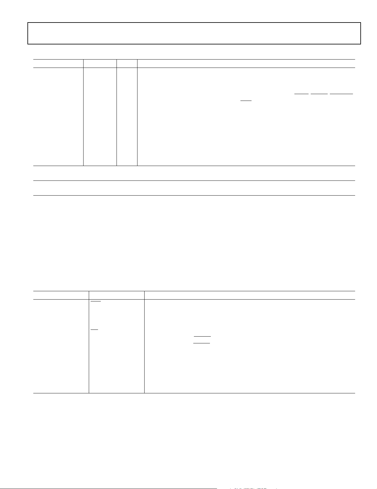
ADSP-TS101S
Table 15. Pin Definitions—Power, Ground, and Reference
Signal Type Term Description
V
DD
V
DD_A
V
DD_IO
V
REF
V
SS
V
SS_A
NC — No connect. Do not connect these pins to anything (not to any supply, signal, or each other),
Type column symbols: A = asynchronous; G = ground; I = input; O = output; o/d = open drain output; P = power supply;
pd = internal pull-down approximately 100 k
Term (for termination) column symbols: epd = external pull-down approximately 10 k
to V
, nc = not connected; au = always used.
DD-IO
PauV
PauV
PauV
pins for internal logic.
DD
pins for analog circuits. Pay critical attention to bypassing this supply.
DD
pins for I/O buffers.
DD
I au Reference voltage defines the trip point for all input buffers, except RESET, IRQ3–0, DMAR3–0,
ID2–0, CONTROLIMP2–0, TCK, TDI, TMS, and TRST
trip point). V
can be connected to a power supply or set by a voltage divider circuit. The
REF
. The value is 1.5 V ± 100 mV (which is the TTL
voltage divider should have an HF decoupling capacitor (1 nF HF SMD) connected to VSS. Tie
the decoupling capacitor between V
input and VSS, as close to the DSP’s pins as possible. For
REF
more information, see Filtering Reference Voltage and Clocks on Page 10.
GauGround pins.
G au Ground pins for analog circuits.
because they are reserved and must be left unconnected.
Ω; pu = internal pull-up approximately 100 kΩ; T = three-state
Ω to V
; epu = external pull-up approximately 10 kΩ
SS
STRAP PIN FUNCTION DESCRIPTIONS
Some pins have alternate functions at reset. Strap options set
DSP operating modes. During reset, the DSP samples the strap
option pins. Strap pins have an approximately 100 kΩ pulldown for the default value. If a strap pin is not connected to an
external pull-up or logic load, the DSP samples the default value
during reset. If strap pins are connected to logic inputs, a stronger external pull-down may be required to ensure default value
Table 16. Pin Definitions—I/O Strap Pins
Signal On Pin … Description
EBOOT BMS
IRQEN BM
TM1 L2DIR Test Mode 1.
TM2 TMR0E Test Mode 2.
EPROM boot.
0 = boot from EPROM immediately after reset (default)
1 = idle after reset and wait for an external device to boot DSP through the
external port or a link port
Interrupt Enable.
0 = disable and set IRQ3–0 interrupts to level sensitive after reset (default)
1 = enable and set IRQ3–0
0 = required setting during reset.
1 = reserved.
0 = required setting during reset.
1 = reserved.
depending on leakage and/or low level input current of the logic
load. To set a mode other than the default mode, connect the
strap pin to a sufficiently stronger external pull-up. In a multiprocessor system, up to eight DSPs may be connected on the
cluster bus, resulting in parallel combination of strap pin pulldown resistors. Table 16 lists and describes each of the DSP’s
strap pins.
interrupts to edge sensitive immediately after reset
Rev. B | Page 19 of 44 | December 2004
Page 20

ADSP-TS101S
SPECIFICATIONS
Note that component specifications are subject to change without notice.
RECOMMENDED OPERATING CONDITIONS
Parameter Test Conditions Min Typ Max Unit
V
DD
V
DD_A
V
DD_IO
T
CASE
V
IH
V
IL
I
DD
I
DD
I
DDIDLELPVDD
I
DD_IO
I
DD_A
V
REF
1
Applies to input and bidirectional pins.
2
For details on internal and external power estimation, including: power vector definitions, current usage descriptions, and formulas, see EE-169, Estimating Power for the
ADSP-TS101S on the Analog Devices website—use site search on “EE-169” (www.analog.com). This document is updated regularly to keep pace with silicon revisions.
Internal Supply Voltage 1.14 1.26 V
Analog Supply Voltage 1.14 1.26 V
I/O Supply Voltage 3.15 3.45 V
Case Operating Temperature –40 +85 ºC
High Level Input Voltage
Low Level Input Voltage
VDD Supply Current for Typical Activity
VDD Supply Current for Typical Activity2@ CCLK = 300 MHz, VDD=1.25 V,
Supply Current for IDLELP
Instruction Execution
V
Supply Current for Typical
DD_IO
2
Activity
V
Supply Current @ VDD=1.25 V, T
DD_A
1
1
@ VDD, V
@ VDD, V
2
@ CCLK = 250 MHz, VDD=1.25 V,
T
CASE
= max 2 V
DD_IO
= min –0.5 +0.8 V
DD_IO
=25ºC
+ 0.5 V
DD_IO
1.2 A
1.5 A
=25ºC
T
CASE
@ CCLK = 300 MHz, VDD=1.20 V,
T
=25ºC
CASE
@ SCLK = 100 MHz, V
T
=25ºC
CASE
CASE
=3.3V,
DD_IO
=25ºC 25 mA
173 mA
137 mA
Voltage Reference 1.4 1.6 V
ELECTRICAL CHARACTERISTICS
Parameter Test Conditions Min Max Unit
V
OH
V
OL
I
IH
I
IHP
I
IL
I
ILP
I
OZH
I
OZHP
I
OZL
I
OZLP
I
OZLO
C
IN
1
Applies to output and bidirectional pins.
2
Applies to input pins with internal pull-downs (pd).
3
Applies to input pins without internal pull-ups (pu).
4
Applies to input pins with internal pull-ups (pu).
5
Applies to three-stateable pins without internal pull-downs (pd).
6
Applies to open drain (od) pins with 500 Ω pull-ups (pu).
7
Applies to three-stateable pins with internal pull-downs (pd).
8
Applies to three-stateable pins without internal pull-ups (pu).
9
Applies to three-stateable pins with internal pull-ups (pu).
10
Applies to all signals.
11
Guaranteed but not tested.
High Level Output Voltage
Low Level Output Voltage
High Level Input Current
High Level Input Current (pd)
Low Level Input Current
Low Level Input Current (pu)
Three-State Leakage Current High
Three-State Leakage Current High (pd)
Three-State Leakage Current Low
Three-State Leakage Current Low (pu)
Three-State Leakage Current Low (od)
Input Capacitance
10, 11
1
1
2
2
3
4
5, 6
7
8
9
7
@V
= min, IOH = –2 mA 2.4 V
DD_IO
@V
= min, IOL=4 mA 0.4 V
DD_IO
@V
=max, VIN=V
DD_IO
@V
=max, VIN=V
DD_IO
@V
=max, VIN=0V 10 µA
DD_IO
@V
=max, VIN=0V –69 –23 µA
DD_IO
@V
=max, VIN=V
DD_IO
@V
=max, VIN=V
DD_IO
@V
@V
@V
@fIN=1MHz, T
=max, VIN=0V 10 µA
DD_IO
=max, VIN=0V –69 –23 µA
DD_IO
=max, VIN = 0 V –9.8 –4.6 mA
DD_IO
CASE
max 10 µA
DD_IO
max 17.2 44.5 µA
DD_IO
max 10 µA
DD_IO
max 17.2 44.5 µA
DD_IO
= 25ºC, VIN=2.5V 5 pF
Rev. B | Page 20 of 44 | December 2004
Page 21

ABSOLUTE MAXIMUM RATINGS
ADSP-TS101S
Internal (Core) Supply Voltage (VDD)
Analog (PLL) Supply Voltage (V
External (I/O) Supply Voltage (V
Input Voltage
Output Voltage Swing
1
1
Storage Temperature Range
1
Stresses greater than those listed above may cause permanent damage to the device.
These are stress ratings only; functional operation of the device at these or any other
conditions greater than those indicated in the operational sections of this specification
is not implied. Exposure to absolute maximum rating conditions for extended periods
may affect device reliability.
1
1
)
DD_A
1
)
DD_IO
1
–0.3 V to +1.40 V
–0.3 V to +1.40 V
–0.3 V to +4.6 V
–0.5 V to V
–0.5 V to V
DD_IO
DD_IO
–65ºC to +150ºC
+0.5 V
+0.5 V
ESD SENSITIVITY
CAUTION
ESD (electrostatic discharge) sensitive device. Electrostatic charges as high as 4000 V readily
accumulate on the human body and test equipment and can discharge without detection. Although
the ADSP-TS101S features proprietary ESD protection circuitry, permanent damage may occur on
devices subjected to high-energy electrostatic discharges. Therefore, proper ESD precautions are
recommended to avoid performance degradation or loss of functionality.
TIMING SPECIFICATIONS
With the exception of link port, IRQ3–0, DMAR3–0, TMR0E,
FLAG3–0 (input), and TRST
TS101S is relative to a reference clock edge. Because input
setup/hold, output valid/hold, and output enable/disable times
are relative to a clock edge, the timing data for the ADSPTS101S has few calculated (formula-based) values. For information on ac timing, see General AC Timing. For information on
link port transfer timing, see Link Ports Data Transfer and
Token Switch Timing on Page 29.
pins, all ac timing for the ADSP-
General AC Timing
Timing is measured on signals when they cross the 1.5 V level as
described in Figure 15 on Page 28. All delays (in nanoseconds)
are measured between the point that the first signal reaches
1.5 V and the point that the second signal reaches 1.5 V.
The ac asynchronous timing data for the IRQ3–0
TMR0E, FLAG3–0 (input), and TRST
pins appears in Table 17.
, DMAR3–0,
The general ac timing data appears in Table 17, Table 25, and
Table 26. All ac specifications are measured with the load speci-
fied in Figure 7, and with the output drive strength set to
strength 4. Output valid and hold are based on standard capacitive loads: 30 pF on all pins. The delay and hold specifications
given should be derated by a drive strength related factor for
loads other than the nominal value of 30 pF.
In order to calculate the output valid and hold times for different load conditions and/or output drive strengths, refer to
Figure 31 on Page 34 through Figure 38 on Page 36 (Rise and
Fall Time vs. Load Capacitance) and Figure 39 on Page 36 (Output Valid vs. Load Capacitance and Drive Strength).
Rev. B | Page 21 of 44 | December 2004
30pF
50⍀
1.5V
TO
OUTPUT
PIN
Figure 7. Equivalent Device Loading for AC Measurements
(Includes All Fixtures)
For power-up sequencing, power-up reset, and normal reset
(hot reset) timing requirements, refer respectively to Table 22
and Figure 12, Table 23 and Figure 13, and Table 24 and
Figure 14.
Page 22

ADSP-TS101S
Table 17. AC Asynchronous Signal Specifications
(All values in this table are in nanoseconds.)
Name Description Pulse Width Low (min) Pulse Width High (min)
1
IRQ3–0
DMAR3–0
TMR0E
FLAG3–0
1
2
1, 3
TRST
1
These input pins do not need to be synchronized to a clock reference.
2
This pin is a strap option. During reset, an internal resistor pulls the pin low.
3
For output specifications, see Table 25 and Table 26.
Table 18. Reference Clocks—Core Clock (CCLK) Cycle Time
Parameter Description
1
t
CCLK
1
CCLK is the internal processor clock or instruction cycle time. The period of this clock is equal to the system clock period (t
(SCLKRAT2–0). For information on available part numbers for different internal processor clock rates, see the Ordering Guide on Page 44.
Core Clock Cycle Time 3.3 12.5 4.0 12.5 ns
Interrupt request input t
DMA request input t
+ 3 ns
CCLK
+ 4 ns t
CCLK
CCLK
Timer 0 expired output 4 × t
Flag pins input 3 × t
ns 3 × t
CCLK
JTAG test reset input 1 ns
Grade = 100 (300MHz) Grade = 000 (250MHz)
) divided by the system clock ratio
SCLK
+ 4 ns
ns
SCLK
ns
CCLK
UnitMin Max Min Max
t
CCLK
CCLK
Figure 8. Reference Clocks—Core Clock (CCLK) Cycle Time
Table 19. Reference Clocks—Local Clock (LCLK) Cycle Time
Parameter Description Min Max Unit
1, 2, 3, 4
t
LCLK
t
LCLKH
t
LCLKL
5, 6
t
LCLKJ
1
For more information, see Table 3 on Page 12.
2
For more information, see Clock Domains on Page 9.
3
LCLK_P and SCLK_P must be connected to the same source.
4
The value of (t
5
Actual input jitter should be combined with ac specifications for accurate timing analysis.
6
Jitter specification is maximum peak-to-peak time interval error (TIE) jitter.
Local Clock Cycle Time 10 25 ns
Local Clock Cycle High Time 0.4 × t
Local Clock Cycle Low Time 0.4 × t
LCLK
LCLK
0.6 × t
0.6 × t
LCLK
LCLK
Local Clock Jitter Tolerance – 500 ps
/ LCLKRAT2-0) must not violate the specification for t
LCLK
t
t
LCLKH
LCLKH
LCLK_P
LCLK_P
t
t
LCLK
LCLK
CCLK
t
t
LCLKL
LCLKL
.
t
t
LCLKJ
LCLKJ
ns
ns
Figure 9. Reference Clocks—Local Clock (LCLK) Cycle Time
Rev. B | Page 22 of 44 | December 2004
Page 23

ADSP-TS101S
Table 20. Reference Clocks—System Clock (SCLK) Cycle Time
Parameter Description Min Max Unit
1, 2, 3, 4
t
SCLK
t
SCLKH
t
SCLKL
5, 6
t
SCLKJ
1
For more information, see Table 3 on Page 12.
2
For more information, see Clock Domains on Page 9.
3
LCLK_P and SCLK_P must be connected to the same source.
4
The value of (t
5
Actual input jitter should be combined with ac specifications for accurate timing analysis.
6
Jitter specification is maximum peak-to-peak time interval error (TIE) jitter.
System Clock Cycle Time 10 25 ns
System Clock Cycle High Time 0.4 × t
System Clock Cycle Low Time 0.4 × t
SCLK
SCLK
0.6 × t
0.6 × t
SCLK
SCLK
System Clock Jitter Tolerance – 500 ps
/ LCLKRAT2-0) must not violate the specification for t
SCLK
t
t
SCLKH
SCLKH
SCLK_P
SCLK_P
Figure 10. Reference Clocks—System Clock (SCLK) Cycle Time
t
t
SCLK
SCLK
CCLK
t
t
SCLKL
SCLKL
.
t
t
SCLKJ
SCLKJ
ns
ns
Table 21. Reference Clocks—Test Clock (TCK) Cycle Time
Parameter Description Min Max Unit
t
TCK
t
TCKH
t
TCKL
Table 22. Power-Up Timing
Test Clock (JTAG) Cycle Time Greater of 30 or t
× 4 – ns
CCLK
Test Clock (JTAG) Cycle High Time 12.5 – ns
Test Clock (JTAG) Cycle Low Time 12.5 – ns
t
TCK
TCK
t
TCKH
Figure 11. Reference Clocks—Test Clock (TCK) Cycle Time
1
t
TCKL
Parameter Min Max Unit
Timing Requirement
t
VDD_IO
V
Stable and Within Specification After VDD and V
DD_IO
>0 ms
DD_A
Are Stable and Within Specification
1
For information about power supply sequencing and monitoring solutions, please visit http://www.analog.com/sequencing.
V
V
DD_IO
V
DD_A
DD
t
VDD_IO
Figure 12. Power-Up Sequencing Timing
Rev. B | Page 23 of 44 | December 2004
Page 24

ADSP-TS101S
Table 23. Power-Up Reset Timing
Parameter Min Max Unit
Timing Requirements
t
START_LO
t
PULSE1_HI
t
PULSE2_LO
1
t
TRST_PWR
1
Applies after VDD, V
V
DD,VDD_A,VDD_IO,
RESET Deasserted After VDD, V
DD_A
, V
, SCLK/LCLK, and
DD_IO
Static/Strap Pins Are Stable and Within Specification
RESET Deasserted for First Pulse 50 × t
RESET Asserted for Second Pulse 100 × t
TRST Asserted During Power-Up Reset 2 × t
, V
DD_A
SCLK /LCLK ,
STAT IC/STRAP
, and SCLK/LCLK and static/strap pins are stable and within specification, and before RESET is deasserted.
DD_IO
t
RESET
TRST
PINS
t
START_LO
t
TRST_PWR
PULSE1_HI
2ms
SCLK
SCLK
SCLK
t
PULSE2_LO
100 × t
SCLK
ns
ns
ns
Figure 13. Power-Up Reset Timing
Table 24. Normal Reset Timing
Parameter Min Max Unit
Timing Requirements
t
RST_IN
t
STRAP
STRAP PINS
RESET Asserted 100 × t
SCLK
RESET Deasserted After Strap Pins Stable 2 ms
t
RST_IN
RESET
t
STRAP
Figure 14. Normal Reset (Hot Reset) Timing
ns
Rev. B | Page 24 of 44 | December 2004
Page 25

Table 25. AC Signal Specifications (for SCLK <16.7 ns)
(All values in this table are in nanoseconds)
ADSP-TS101S
2
Name Description
Input Setup
(min)
Input Hold
(min)
Output Valid
(max)1Output Hold
(min)
Output Enable
(min)
Output Disable
(max)2Reference
Clock
ADDR31–0 External Address Bus 2.6 0.5 4.2 1.0 0.9 2.5 SCLK
DATA63–0 External Data Bus 2.6 0.5 4.2 1.0 0.9 2.5 SCLK
MSH
MSSD
MS1–0
RD
WRL
WRH
Memory Select Host Line 4.2 1.0 0.9 2.5 SCLK
Memory Select SDRAM Line 2.6 0.5 4.2 1.0 0.9 2.5 SCLK
Memory Select for Static Blocks 4.2 1.0 0.9 2.5 SCLK
Memory Read 2.6 0.5 4.2 1.0 0.9 2.5 SCLK
Write Low Word 2.6 0.5 4.2 1.0 0.9 2.5 SCLK
Write High Word 2.6 0.5 4.2 1.0 0.9 2.5 SCLK
ACK Acknowledge for Data 2.6 0.5 4.2 1.0 0.9 2.5 SCLK
SDCKE SDRAM Clock Enable 2.6 0.5 4.2 1.0 0.9 2.5 SCLK
RAS
CAS
SDWE
Row Address Select 2.6 0.5 4.2 1.0 0.9 2.5 SCLK
Column Address Select 2.6 0.5 4.2 1.0 0.9 2.5 SCLK
SDRAM Write Enable 2.6 0.5 4.2 1.0 0.9 2.5 SCLK
LDQM Low Word SDRAM Data Mask 4.2 1.0 0.9 2.5 SCLK
HDQM High Word SDRAM Data Mask 4.2 1.0 0.9 2.5 SCLK
SDA10 SDRAM ADDR10 4.2 1.0 0.9 2.5 SCLK
HBR
HBG
BOFF
BUSLOCK
BRST
BR7–0
FLYBY
IOEN
3, 4
CPA
3, 4
DPA
5
BMS
FLAG3–0
4, 7
RESET
4
TMS
4
TDI
6
Host Bus Request 2.6 0.5 SCLK
Host Bus Grant 2.6 0.5 4.2 1.0 0.9 2.5 SCLK
Back Off Request 2.6 0.5 SCLK
Bus Lock 4.2 1.0 0.9 2.5 SCLK
Burst Access 2.6 0.5 4.2 1.0 0.9 2.5 SCLK
Multiprocessing Bus Request 2.6 0.5 4.2 1.0 SCLK
Flyby Mode Selection 4.2 1.0 0.9 2.5 SCLK
Flyby I/O Enable 4.2 1.0 0.9 2.5 SCLK
Core Priority Access 2.6 0.5 5.8 2.5 SCLK
DMA Priority Access 2.6 0.5 5.8 2.5 SCLK
Boot Memory Select 4.2 1.0 0.9 2.5 SCLK
FLAG Pins 4.2 1.0 1.0 4.0 SCLK
Global Reset SCLK
Test Mode Select (JTAG) 1.5 1.0 TCK
Test Data Input (JTAG) 1.5 1.0 TCK
TDO Test Data Output (JTAG) 6.0 1.0 1.0 5.0 TCK_FE
4, 7, 9
TRST
5
BM
10
EMU
JTAG_SYS_IN
11
JTAG_SYS_OUT
9
ID2–0
CONTROLIMP2–0
12
9
Test Reset (JTAG) TCK
Bus Master Debug Aid Only 4.2 1.0 SCLK
Emulation 5.5 5.0 TCK or LCLK
System Input 1.5 11.0 TCK
System Output 16.0 TCK_FE
Chip ID—Must Be Constant
Static Pins—Must Be Constant
8
8
Rev. B | Page 25 of 44 | December 2004
Page 26

ADSP-TS101S
Table 25. AC Signal Specifications (for SCLK <16.7 ns) (Continued)
(All values in this table are in nanoseconds)
2
Name Description
9
DS2–0
LCLKRAT2–0
SCLKFREQ
1
The output valid (max) value in this column applies for the standard 30 pF capacitive load used in testing. To see how output valid varies with capacitive loading, see Figure 39
on Page 36.
2
The external port protocols employ bus IDLE cycles for bus mastership transitions as well as slave address boundary crossings to avoid any potential bus contention. The
apparent driver overlap, due to output disables being larger than output enables, is not actual.
3
CPA and DPA pins are open drains and have 0.5 kΩ internal pull-ups.
4
These input pins have Schmitt triggers and therefore do not need to be synchronized to a clock reference. These synchronous specifications only apply for recognition in the
current clock reference cycle.
5
This pin is a strap option. During reset, an internal resistor pulls the pin low.
6
For input specifications, see Table 17.
7
For additional requirement details, see Reset and Booting on Page 9.
8
TCK_FE indicates TCK falling edge.
9
These pins may change only during reset; recommend connecting it to V
10
Reference clock depends on function.
11
System inputs are: IRQ3–0, BMS, LCLKRAT2–0, SCLKFREQ, BM, TMR0E, FLAG3–0, ID2–0, BRST, WRH, WRL, RD, MSSD, SDCKE, SDWE, CAS, RAS, ADDR31–0,
DATA63–0, DPA, CPA, HBG, BOFF, HBR, ACK, BR7–0, L0CLKIN, L0DAT7–0, L1CLKIN, L1DAT7–0, L2CLKIN, L2DAT7–0, L2DIR, L3CLKIN, L3DAT7–0, DS2–0,
CONTROLIMP2–0, RESET, DMAR3–0.
12
System outputs are: BMS, BM, BUSLOCK, TMR0E, FLAG3–0, FLYBY, IOEN, MSH, BRST, WRH, WRL, RD, MS1–0, HDQM, LDQM, MSSD, SDCKE, SDWE, CAS, RAS,
ADDR31–0, DATA63–0, DPA, CPA, HBG, ACK, BR7–0, L0CLKOUT, L0DAT7–0, L0DIR, L1CLKOUT, L1DAT7–0, L1DIR, L2CLKOUT, L2DAT7–0, L2DIR, L3CLKOUT,
L3DAT7–0, L3DIR, EMU.
9
9
Static Pins—Must Be Constant
Static Pins—Must Be Constant
Static Pins—Must Be Constant
DD_IO/VSS
Input Setup
(min)
Input Hold
(min)
Output Valid
(max)1Output Hold
.
(min)
Output Enable
(min)
Output Disable
(max)2Reference
Clock
Rev. B | Page 26 of 44 | December 2004
Page 27

Table 26. AC Signal Specifications (for 16.7 ns <SCLK <25 ns)
(All values in this table are in nanoseconds)
ADSP-TS101S
2
Name Description
Input Setup
(min)
Input Hold
(min)
Output Valid
(max)1Output Hold
(min)
Output Enable
(min)
Output Disable
(max)2Reference
Clock
ADDR31–0 External Address Bus 2.8 0.5 4.2 0.8 0.3 2.5 SCLK
DATA63–0 External Data Bus 2.8 0.5 4.2 0.8 0.3 2.5 SCLK
MSH
MSSD
MS1–0
RD
WRL
WRH
Memory Select Host Line 4.2 0.8 0.3 2.5 SCLK
Memory Select SDRAM Line 2.8 0.5 4.2 0.8 0.3 2.5 SCLK
Memory Select for Static Blocks 4.2 0.8 0.3 2.5 SCLK
Memory Read 2.8 0.5 4.2 0.8 0.3 2.5 SCLK
Write Low Word 2.8 0.5 4.2 0.8 0.3 2.5 SCLK
Write High Word 2.8 0.5 4.2 0.8 0.3 2.5 SCLK
ACK Acknowledge for Data 2.8 0.5 4.2 0.8 0.3 2.5 SCLK
SDCKE SDRAM Clock Enable 2.8 0.5 4.2 0.8 0.3 2.5 SCLK
RAS
CAS
SDWE
Row Address Select 2.8 0.5 4.2 0.8 0.3 2.5 SCLK
Column Address Select 2.8 0.5 4.2 0.8 0.3 2.5 SCLK
SDRAM Write Enable 2.8 0.5 4.2 0.8 0.3 2.5 SCLK
LDQM Low Word SDRAM Data Mask 4.2 0.8 0.3 2.5 SCLK
HDQM High Word SDRAM Data Mask 4.2 0.8 0.3 2.5 SCLK
SDA10 SDRAM ADDR10 4.2 0.8 0.3 2.5 SCLK
HBR
HBG
BOFF
BUSLOCK
BRST
BR7–0
FLYBY
IOEN
3, 4
CPA
3, 4
DPA
5
BMS
FLAG3–0
4, 7
RESET
4
TMS
4
TDI
6
Host Bus Request 2.8 0.5 SCLK
Host Bus Grant 2.8 0.5 4.2 0.8 0.3 2.5 SCLK
Back Off Request 2.8 0.5 SCLK
Bus Lock 4.2 0.8 0.3 2.5 SCLK
Burst Access 2.8 0.5 4.2 0.8 0.3 2.5 SCLK
Multiprocessing Bus Request 2.8 0.5 4.2 0.8 SCLK
Flyby Mode Selection 4.2 0.8 0.3 2.5 SCLK
Flyby Mode I/O Enable 4.2 0.8 0.3 2.5 SCLK
Core Priority Access 2.8 0.5 5.8 2.5 SCLK
DMA Priority Access 2.8 0.5 5.8 2.5 SCLK
Boot Memory Select 4.2 0.8 0.3 2.5 SCLK
FLAG Pins 4.2 1.0 1.0 4.0 SCLK
Global Reset SCLK
Test Mode Select (JTAG) 1.5 1.0 TCK
Test Data Input (JTAG) 1.5 1.0 TCK
TDO Test Data Output (JTAG) 6.0 1.0 1.0 5.0 TCK_FE
4, 7, 9
TRST
5
BM
10
EMU
JTAG_SYS_IN
11
JTAG_SYS_OUT
9
ID2–0
CONTROLIMP2–0
12
9
Test Reset (JTAG) TCK
Bus Master Debug Aid Only 4.2 0.8 SCLK
Emulation 5.5 5.0 TCK or LCLK
System Input 1.5 11.0 TCK
System Output 16.0 TCK_FE
Chip ID—Must Be Constant
Static Pins—Must Be Constant
8
8
Rev. B | Page 27 of 44 | December 2004
Page 28

ADSP-TS101S
Table 26. AC Signal Specifications (for 16.7 ns <SCLK <25 ns) (Continued)
(All values in this table are in nanoseconds)
2
Name Description
9
DS2–0
LCLKRAT2–0
SCLKFREQ
1
The output valid (max) value in this column applies for the standard 30 pF capacitive load used in testing. To see how output valid varies with capacitive loading, see Figure 39
on Page 36.
2
The external port protocols employ bus IDLE cycles for bus mastership transitions as well as slave address boundary crossings to avoid any potential bus contention. The
apparent driver overlap, due to output disables being larger than output enables, is not actual.
3
CPA and DPA pins are open drains and have 0.5 kΩ internal pull-ups.
4
These input pins have Schmitt triggers and therefore do not need to be synchronized to a clock reference. These synchronous specifications only apply for recognition in the
current clock reference cycle.
5
This pin is a strap option. During reset, an internal resistor pulls the pin low.
6
For input specifications, see Table 17.
7
For additional requirement details, see Reset and Booting on Page 9.
8
TCK_FE indicates TCK falling edge.
9
These pins may change only during reset; recommend connecting it to V
10
Reference clock depends on function.
11
System inputs are: IRQ3–0, BMS, LCLKRAT2–0, SCLKFREQ, BM, TMR0E, FLAG3–0, ID2–0, BRST, WRH, WRL, RD, MSSD, SDCKE, SDWE, CAS, RAS, ADDR31–0,
9
9
Static Pins—Must Be Constant
Static Pins—Must Be Constant
Static Pins—Must Be Constant
DD_IO/VSS
Input Setup
(min)
Input Hold
(min)
Output Valid
(max)1Output Hold
(min)
Output Enable
(min)
Output Disable
(max)2Reference
Clock
.
DATA63–0, DPA, CPA, HBG, BOFF, HBR, ACK, BR7–0, L0CLKIN, L0DAT7–0, L1CLKIN, L1DAT7–0, L2CLKIN, L2DAT7–0, L2DIR, L3CLKIN, L3DAT7–0, DS2–0,
CONTROLIMP2–0, RESET, DMAR3–0.
12
System outputs are: BMS, BM, BUSLOCK, TMR0E, FLAG3–0, FLYBY, IOEN, MSH, BRST, WRH, WRL, RD, MS1–0, HDQM, LDQM, MSSD, SDCKE, SDWE, CAS, RAS,
ADDR31–0, DATA63–0, DPA, CPA, HBG, ACK, BR7–0, L0CLKOUT, L0DAT7–0, L0DIR, L1CLKOUT, L1DAT7–0, L1DIR, L2CLKOUT, L2DAT7–0, L2DIR, L3CLKOUT,
L3DAT7–0, L3DIR, EMU.
REFERENCE
CLOCK
1.5V
INPUT
SIGNAL
OUTPUT
SIGNAL
THREE-STATE
ASYNCHRONOUS
INPUT OR
OUTPUT
SIGNAL
INPUT
SETUP
PULSE WIDTH
OUTPUT
VALID
OUTPUT
DISABLE
1.5V
1.5V
1.5V
Figure 15. General AC Parameters Timing
Rev. B | Page 28 of 44 | December 2004
INPUT
HOLD
OUTPUT
HOLD
OUTPUT
ENABLE
Page 29

ADSP-TS101S
Link Ports Data Transfer and Token Switch Timing
Table 27, Table 28, Table 29, and Table 30 with Figure 16,
Figure 17, Figure 18, and Figure 19 provide the timing specifica-
tions for the link ports data transfer and token switch.
Table 27. Link Ports—Transmit
Parameter Min Max Unit
Timing Requirements
1
t
CONNS
2
t
CONNS
3
t
CONNIW
t
ACKS
Switching Characteristics
4
t
LXCLK_T
X
1
t
LXCLKH_T
X
2
t
LXCLKH_T
X
1
t
LXCLKL_T
X
2
t
LXCLKL_T
X
t
DIRS
t
DIRH
1
t
DOS
1
t
DOH
2
t
DOS
2
t
DOH
t
LDOE
5
t
LDOD
1
The formula for this parameter applies when LR is 2.
2
The formula for this parameter applies when LR is 3, 4, or 8.
3
LxCLKIN shows the connectivity pulse with each of the three possible transitions to “Acknowledge.” After a connectivity pulse low minimum, LxCLKIN may [1] return high
and remain high for “Acknowledge,” [2] return high and subsequently go low (meeting t
4
The Link clock Ratio (LR) is 2, 3, 4, or 8 as set by the SPD bits in the LCTLx register. The maximum LxCLK is 125 MHz. LR = 2 may not be used when CCLK ≥ 250 MHz.
5
This specification applies to the last data byte or the “Dummy” byte that follows the verification byte if enabled. For more information, see the ADSP-TS101 TigerSHARC
Processor Hardware Reference.
Connectivity Pulse Setup 2 × t
+ 3.5 ns
CCLK
Connectivity Pulse Setup 8 ns
Connectivity Pulse Input Width t
Acknowledge Setup 0.5 × t
Transmit Link Clock Period 0.9 × LR × t
Transmit Link Clock Width High 0.33 × t
Transmit Link Clock Width High 0.4 × t
Transmit Link Clock Width Low 0.33 × t
Transmit Link Clock Width Low 0.4 × t
LxDIR Transmit Setup 0.5 × t
LxDIR Transmit Hold 0.5 × t
LxDAT7–0 Output Setup 0.25 × t
LxDAT7–0 Output Hold 0.25 × t
LxDAT7–0 Output Setup Greater of 0.8 or 0.17 × t
LxDAT7–0 Output Hold Greater of 0.8 or 0.17 × t
+ 1 ns
LXCLK_T
X
LXCLK_T
X
CCLK
LXCLK_T
X
LXCLK_T
X
LXCLK_T
X
LXCLK_T
X
LXCLK_T
X
LXCLK_T
X
– 1 ns
LXCLK_T
X
– 1 ns
LXCLK_T
X
LXCLK_T
LXCLK_T
1.1 × LR × t
0.66 × t
0.6 × t
0.66 × t
0.6 × t
2 × t
LXCLK_T
2 × t
LXCLK_T
– 1 ns
X
– 1 ns
X
LXCLK_T
LXCLK_T
LXCLK_T
LXCLK_T
ns
ns
CCLK
ns
X
ns
X
ns
X
ns
X
ns
X
ns
X
LxDAT7–0 Output Enable 1 ns
LxDAT7–0 Output Disable 1 ns
) for “Not Acknowledge,” or [3] remain low for “Not Acknowledge.”
ACKS
LxCLKOUT
LxCLKIN
LxDAT7–0
LxDIR
t
DIRS
t
LDOE
t
LxCLK H_Tx
1
t
t
LxCLK_Tx
2
3
t
LxCLKL_Tx
5
40
t
DOS
6
t
CONNIW
CONNS
t
DOH
7
8
Figure 16. Link Ports—Transmit
Rev. B | Page 29 of 44 | December 2004
t
t
ACKS
t
DOH
t
DOS
9
11
10
13
12
14
DIRH
15
t
LDOD
Page 30

ADSP-TS101S
Table 28. Link Ports—Receive
Parameter Min Max Unit
Timing Requirements
1, 2
t
LXCLK_R
X
3
t
LXCLKH_R
X
4
t
LXCLKH_R
X
3
t
LXCLKL_R
X
4
t
LXCLKL_R
X
t
DIS
t
DIH
Switching Characteristics
t
CONNV
t
CONNOW
1
The link clock ratio (LR) is 2, 3, 4, or 8 as set by the SPD bits in the LCTLx register.
2
The maximum LxCLK is 125 MHz. LR = 2 may not be used when CCLK ≥ 250 MHz.
3
The formula for this parameter applies when LR is 2.
4
The formula for this parameter applies when LR is 3, 4, or 8.
Receive Link Clock Period 0.9 × LR × t
Receive Link Clock Width High 0.33 × t
Receive Link Clock Width High 0.4 × t
Receive Link Clock Width Low 0.33 × t
Receive Link Clock Width Low 0.4 × t
LXCLK_R
LXCLK_R
LXCLK_R
LXCLK_R
CCLK
X
X
X
X
1.1 × LR × t
0.66 × t
LXCLK_R
0.6 × t
LXCLK_R
0.66 × t
LXCLK_R
0.6 × t
LXCLK_R
CCLK
X
X
X
X
LxDAT7–0 Input Setup 0.6 ns
LxDAT7–0 Input Hold 0.6 ns
Connectivity Pulse Valid 0 2.5 × t
Connectivity Pulse Output Width 1.5 × t
t
LxCLK_Rx
t
LxCLKH_Rx
t
LxCLKL_Rx
3
4
t
DIS
5
7
6
LxCLKIN
LxCLKOUT
t
CONNV
1
2
t
CONNOW
LXCLK_R
X
t
DIH
9
80
t
DIH
t
DIS
11
10
13
12
LXCLK_R
X
15
14
ns
ns
ns
ns
ns
ns
ns
LxDAT7–0
LxDIR
Figure 17. Link Ports—Receive
Rev. B | Page 30 of 44 | December 2004
Page 31

ADSP-TS101S
Table 29. Link Ports—Token Switch, Token Master
Parameter Min Max Unit
Timing Requirements
t
REQI
t
TKRQ
Switching Characteristics
t
TKENO
t
REQO
1
For guaranteeing token switch during token enable.
2
LxCLKOUT shows both possible responses to the token request: [1] a “Token Grant” (LxCLKOUT remains high), and [2] a “Token Regret” (LxCLKOUT goes low).
Token Request Input Width 5.0 × t
Token Request from Token Enable
1
Token Switch Enable Output 8.0 × t
Token Request Output Width
2
6.0 × t
LXCLK_R
LXCLK_T
LXCLK_T
X
3.0 × t
LXCLK_T
X
X
X
ns
ns
ns
ns
LxCLKOUT
LxCLKIN
t
TKENO
15
14
t
TKRQ
t
REQI
t
REQO
Figure 18. Link Ports—Token Switch, Token Master
Table 30. Link Ports—Token Switch, Token Requester
Parameter Min Max Unit
Timing Requirements
1
t
TKENI
Token Switch Enable Input 8.0 × t
LXCLK_R
X
ns
Switching Characteristics
t
REQO
1
Required whenever there is a break in transmission.
2
LxCLKOUT shows both possible responses to the token request: [1] a “Token Grant” (LxCLKOUT remains high), and [2] a “Token Regret” (LxCLKOUT goes low).
Token Request Output Width
LxCLKIN
(FOR TOKEN
REGRET)
LxCLKOUT
(FOR TOKEN
REGRET)
LxCLKIN
(FOR TOKEN
GRANT)
LxCLKOUT
(FOR TOKEN
GRANT)
13 15
13 15
2
t
TKENI
1412
1412
t
t
TKRQ
TKRQ
t
TKENI
6.0 × t
LXCLK_R
t
t
REQO
REQO
X
t
REQO
1
0
3
2
ns
Figure 19. Link Ports—Token Switch, Token Requester
Rev. B | Page 31 of 44 | December 2004
Page 32

ADSP-TS101S
OUTPUT DRIVE CURRENTS
Figure 20 through Figure 27 show typical I–V characteristics for
the output drivers of the ADSP-TS101S. The curves in these diagrams represent the current drive capability of the output
drivers as a function of output voltage over the range of drive
strengths. For complete output driver characteristics, refer to
IBIS models, available on the Analog Devices website,
www.analog.com.
30
25
20
15
10
A
m
–
T
N
E
R
R
–5
U
C
–10
N
I
P
T
–15
U
P
T
–20
U
O
–25
–30
I
OL
5
V
= 3.15V, +85°C
DD_IO
0
V
=3.15V,+85°C
DD_IO
03.50.5 1.0 1.5 2.0 2.5 3.0
Figure 20. Typical Drive Currents at Strength 0
60
50
40
30
A
m
20
–
T
N
10
E
R
R
U
C
–10
N
I
P
–20
T
U
P
–30
T
U
O
–40
–50
–60
–70
I
OL
V
= 3.15V, +85°C
DD_IO
0
V
=3.15V,+85°C
DD_IO
03.50.5 1.0 1.5 2.0 2.5 3.0
STRENGTH 0
V
V
=3.3V,+25°C
DD_IO
V
V
=3.3V,+25°C
DD_IO
OUTPUT PIN VOLTAGE – V
STRENGTH 1
V
V
=3.3V,+25°C
DD_IO
V
V
=3.3V,+25°C
DD_IO
OUTPUT PIN VOLTAGE – V
=3.45V,–40°C
DD_IO
DD_IO
DD_IO
DD_IO
= 3.45V, –40°C
I
OH
= 3.45V, –40°C
= 3.45V, –40°C
I
OH
80
60
40
A
m
–
20
T
N
E
R
R
U
C
N
–20
I
P
T
U
–40
P
T
U
O
–60
–80
–100
I
OL
V
= 3.15V, +85°C
DD_IO
0
V
=3.15V,+85°C
DD_IO
03.50.5 1.0 1.5 2.0 2.5 3.0
STRENGTH 2
V
=3.3V,+25°C
DD_IO
V
=3.3V,+25°C
DD_IO
OUTPUT PIN VOLTAGE – V
Figure 22. Typical Drive Currents at Strength 2
125
100
75
A
m
50
–
T
N
E
25
R
R
U
C
N
I
P
–25
T
U
P
–50
T
U
O
–75
–100
–125
I
OL
V
= 3.15V, +85°C
DD_IO
0
V
=3.15V,+85°C
DD_IO
03.50.5 1.0 1.5 2.0 2.5 3.0
STRENGTH 3
V
=3.3V,+25°C
DD_IO
V
=3.3V,+25°C
DD_IO
OUTPUT PIN VOLTAGE – V
Figure 23. Typical Drive Currents at Strength 3
V
V
V
V
DD_IO
DD_IO
DD_IO
DD_IO
= 3.45V, –40°C
= 3.45V, –40°C
I
OH
= 3.45V, –40°C
= 3.45V, –40°C
I
OH
Figure 21. Typical Drive Currents at Strength 1
Rev. B | Page 32 of 44 | December 2004
Page 33

ADSP-TS101S
140
STRENGTH 4
120
I
OL
100
80
A
60
m
–
40
T
N
20
E
R
R
U
C
N
I
P
T
U
P
T
U
O
–20
–40
–60
–80
–100
V
= 3.15V, +85°C
DD_IO
0
V
=3.15V,+85°C
DD_IO
V
DD_IO
V
DD_IO
=3.3V,+25°C
=3.3V,+25°C
–120
–140
–160
03.50.5 1.0 1.5 2.0 2.5 3.0
OUTPUT PIN VOLTAGE – V
Figure 24. Typical Drive Currents at Strength 4
160
140
I
OL
120
100
80
A
m
60
–
T
40
N
E
20
R
R
U
C
N
I
P
T
U
P
T
U
O
–20
–40
–60
–80
–100
V
= 3.15V, +85°C
DD_IO
0
V
=3.15V,+85°C
DD_IO
–120
–140
–160
–180
03.50.5 1.0 1.5 2.0 2.5 3.0
STRENGTH 5
V
=3.3V,+25°C
DD_IO
V
=3.3V,+25°C
DD_IO
OUTPUT PIN VOLTAGE – V
Figure 25. Typical Drive Currents at Strength 5
V
V
V
V
DD_IO
DD_IO
DD_IO
DD_IO
=3.45V,–40°C
= 3.45V, –40°C
I
OH
= 3.45V, –40°C
= 3.45V, –40°C
I
OH
180
A
m
–
T
N
E
R
R
U
C
N
I
P
T
U
P
T
U
O
160
140
120
100
–20
–40
–60
–80
–100
–120
–140
–160
–180
–200
–220
80
60
40
20
I
OL
V
=3.3V,+25°C
DD_IO
V
= 3.15V, +85°C
DD_IO
0
V
=3.3V,+25°C
DD_IO
V
=3.15V,+85°C
DD_IO
03.50.5 1.0 1.5 2.0 2.5 3.0
OUTPUT PIN VOLTAGE – V
Figure 26. Typical Drive Currents at Strength 6
STRENGTH 6
220
A
m
–
T
N
E
R
R
U
C
N
I
P
T
U
P
T
U
O
200
180
160
140
120
100
–20
–40
–60
–80
–100
–120
–140
–160
–180
–200
–220
80
60
40
20
I
OL
V
= 3.15V, +85°C
DD_IO
0
V
=3.15V,+85°C
DD_IO
03.50.5 1.0 1.5 2.0 2.5 3.0
STRENGTH 7
V
=3.3V,+25°C
DD_IO
V
=3.3V,+25°C
DD_IO
OUTPUT PIN VOLTAGE – V
Figure 27. Typical Drive Currents at Strength 7
V
V
V
V
DD_IO
DD_IO
DD_IO
DD_IO
= 3.45V, –40°C
= 3.45V, –40°C
I
OH
= 3.45V, –40°C
= 3.45V, –40°C
I
OH
Rev. B | Page 33 of 44 | December 2004
Page 34

ADSP-TS101S
TEST CONDITIONS
The test conditions for timing parameters appearing in Table 25
on Page 25 and Table 26 on Page 27 include output disable time,
output enable time, and capacitive loading. The timing specifications for the DSP apply for the voltage reference levels in
Figure 28.
INPUT
OR
OUTPUT
Figure 28. Voltage Reference Levels for AC Measurements (Except
Output Enable/Disable)
REFERENCE
V
V
1.5V 1.5V
SIGNAL
t
MEASURED_DIS
t
DIS
OH (MEASURED)
OL (MEASURED)
V
OH (MEASURED)
V
OL (MEASURED)
t
DECAY
t
– ⌬V
+ ⌬V
ENA
t
MEASURED_ENA
2.0V
1.0V
t
RAMP
CLV∆
t
The output enable time t
t
MEASURED_ENA
t
MEASURED_ENA
and t
RAMP
is the interval from when the reference signal
RAMP
ENA
as shown in Figure 29. The time
---------------
=
I
D
is the difference between
switches to when the output voltage ramps ∆V from the measured three-stated output level. The t
with test load C
, drive current ID, and with ∆V equal to 0.5 V.
L
value is calculated
RAMP
Capacitive Loading
Figure 30 shows the circuit with variable capacitance that is
used for measuring typical output rise and fall times. Figure 31
through Figure 38 show how output rise time varies with capacitance. Figure 39 graphically shows how output valid varies with
load capacitance. (Note that this graph or derating does not
apply to output disable delays; see Output Disable Time on
Page 34.) The graphs of Figure 31 through Figure 39 may not be
linear outside the ranges shown.
TO
OUTPUT
PIN
VARIABLE
(10pF to 100pF)
1.5V
OUTPUT STOPS
DRIVING
HIGH IMPEDANCE STATE.
TEST CONDITIONS CAUSE THIS
VOLTAGE TO BE APPROXIMATELY 1.5V.
OUTPUT STARTS
DRIVING
Figure 29. Output Enable/Disable
Output Disable Time
Output pins are considered to be disabled when they stop driving, go into a high impedance state, and start to decay from their
output high or low voltage. The time for the voltage on the bus
to decay by ∆V is dependent on the capacitive load, C
load current, I
. This decay time can be approximated by the fol-
L
and the
L
lowing equation:
CLV∆
t
DECAY
The output disable time t
t
MEASURED_DIS
t
MEASURED_DIS
and t
as shown in Figure 29. The time
DECAY
is the interval from when the reference signal
DIS
---------------
=
I
L
is the difference between
switches to when the output voltage decays ∆V from the measured output high or output low voltage. The t
calculated with test loads C
and IL, and with ∆V equal to 0.5 V.
L
DECAY
value is
Output Enable Time
Output pins are considered to be enabled when they have made
a transition from a high impedance state to when they start driv-
∆
ing. The time for the voltage on the bus to ramp by
dependent on the capacitive load, C
, and the drive current, ID.
L
V is
This ramp time can be approximated by the following equation:
Figure 30. Equivalent Device Loading for AC Measurements
(Includes All Fixtures)
25
s
n
20
–
S
E
M
I
T
15
L
L
A
F
D
N
10
A
E
S
I
R
5
0
RISE TIME
y = 0.2015x + 3.8869
0
10 20 30 40 50 60 70 80 90 100
STRENGTH 0
=3.3V)
(V
DD_IO
LOAD CAPACITANCE – pF
FALL TIME
y = 0.174x + 2.6931
Figure 31. Typical Output Rise and Fall Time (10%–90%, V
Load Capacitance at Strength 0
DD_IO
=3.3V) vs.
Rev. B | Page 34 of 44 | December 2004
Page 35

ADSP-TS101S
25
s
n
20
–
S
E
M
I
T
L
15
L
A
F
D
N
A
10
E
S
I
R
5
0
0
RISE TIME
y = 0.1349x + 1.9955
10 20 70 80 90 100
STRENGTH 1
=3.3V)
(V
DD_IO
30 40
50 60
LOAD CAPACITANCE – pF
FALL TIME
y = 0.1163x + 1.4058
Figure 32. Typical Output Rise and Fall Time (10%–90%, V
Load Capacitance at Strength 1
25
s
n
20
–
S
E
M
I
T
15
L
L
A
F
D
N
A
10
E
S
I
R
5
0
0 10203040506070 8090100
RISE TIME
y = 0.1304x + 0.8427
STRENGTH 2
=3.3V)
(V
DD_IO
y = 0.1144x + 0.7025
LOAD CAPACITANCE – pF
FALL TIME
Figure 33. Typical Output Rise and Fall Time (10%–90%, V
Load Capacitance at Strength 2
DD_IO
DD_IO
= 3.3 V) vs.
= 3.3 V) vs.
25
s
n
20
–
S
E
M
I
T
15
L
L
A
F
D
N
10
A
E
S
I
y = 0.1071x + 0.9877
R
5
RISE TIME
STRENGTH 4
=3.3V)
(V
DD_IO
FALL TIME
y = 0.0798x + 1.0743
0
0 10203040 5060708090100
LOAD CAPACITANCE – pF
Figure 35. Typical Output Rise and Fall Time (10%–90%, V
Load Capacitance at Strength 4
25
s
n
20
–
S
E
M
I
T
15
L
L
A
F
D
N
10
A
E
S
I
R
y = 0.1001x + 0.7763
5
0
0
10 20 30 40 50 60 70 80 90 100
RISE TIME
STRENGTH 5
(V
=3.3V)
DD_IO
LOAD CAPACITANCE – pF
FALL TIME
y = 0.0793x + 0.8691
Figure 36. Typical Output Rise and Fall Time (10%–90%, V
Load Capacitance at Strength 5
DD_IO
DD_IO
=3.3V) vs.
=3.3V) vs.
25
s
n
20
–
S
E
M
I
T
15
L
L
A
F
D
N
10
A
E
S
I
R
5
0
RISE TIME
y = 0.1082x + 1.3123
0
10 20 30 40 50 60 70 80 90 100
STRENGTH 3
=3.3V)
(V
DD_IO
LOAD CAPACITANCE – pF
FALL TIME
y = 0.0912x + 1.2048
Figure 34. Typical Output Rise and Fall Time (10%–90%, V
Load Capacitance at Strength 3
25
s
n
20
–
S
E
M
I
T
15
L
L
A
F
D
N
10
A
E
S
I
R
5
0
0
= 3.3 V) vs.
DD_IO
Figure 37. Typical Output Rise and Fall Time (10%–90%, V
Load Capacitance at Strength 6
Rev. B | Page 35 of 44 | December 2004
STRENGTH 6
(V
=3.3V)
DD_IO
RISE TIME
y = 0.0946x + 1.2187
10 20 30 40 50 60 70 80 90 100
LOAD CAPACITANCE – pF
FALL TIME
y = 0.0906x + 0.4597
DD_IO
=3.3V) vs.
Page 36

ADSP-TS101S
25
s
n
20
–
S
E
M
I
T
15
L
L
A
F
D
N
A
10
E
S
I
R
5
0
RISE TIME
y = 0.0907x + 1.0071
0102030405060708090100
STRENGTH 7
=3.3V)
(V
DD_IO
LOAD CAPACITANCE – pF
FALL TIME
y = 0.09x + 0.3134
Figure 38. Typical Output Rise and Fall Time (10%–90%, V
Load Capacitance at Strength 7
15
s
10
n
–
D
I
L
A
V
T
U
P
T
U
5
O
STRENGTH 0-7
(V
=3.3V)
DD_IO
DD_IO
= 3.3 V) vs.
0
1
2
3
4
5
6
7
ENVIRONMENTAL CONDITIONS
The ADSP-TS101S is rated for performance over the extended
commercial temperature range, T
Thermal Characteristics
The ADSP-TS101S is packaged in a 19 mm × 19 mm and
27 mm × 27 mm Plastic Ball Grid Array (PBGA). The ADSPTS101S is specified for a case temperature (T
that the T
data sheet specification is not exceeded, a heat
CASE
sink and/or an air flow source may be used. See Table 31 and
Table 32 for thermal data.
Table 31. Thermal Characteristics
for 19 mm × 19 mm Package
Parameter Condition Typical Unit
1
θ
JA
θ
JC
θ
JB
1
Determination of parameter is system dependent and is based on a number of
factors, including device power dissipation, package thermal resistance, board
thermal characteristics, ambient temperature, and air flow.
2
Per JEDEC JESD51-2 procedure using a four layer board (compliant with JEDEC
JESD51-9).
3
Per SEMI Test Method G38-87 using a four layer board (compliant with JEDEC
JESD51-9).
Airflow2 = 0 m/s
3
Airflow
Airflow
= 1 m/s
3
= 2 m/s 12.9 °C/W
= –40°C to +85°C.
CASE
CASE
16.6 °C/W
14.0 °C/W
6.7 °C/W
5.8 °C/W
). To ensure
0
0 102030405060708090100
LOAD CAPACITANCE – pF
Figure 39. Typical Output Valid (V
Case Temperature and Strength 0–7
1
The line equations for the output valid vs. load capacitance are:
= 3.3 V) vs. Load Capacitance at Max
DD_IO
1
Strength 0: y = 0.0956x + 3.5662
Strength 1: y = 0.0523x + 3.2144
Strength 2: y = 0.0433x + 3.1319
Strength 3: y = 0.0391x + 2.9675
Strength 4: y = 0.0393x + 2.7653
Strength 5: y = 0.0373x + 2.6515
Strength 6: y = 0.0379x + 2.1206
Strength 7: y = 0.0399x + 1.9080
PBGA PIN CONFIGURATIONS
The 484-ball PBGA pin configurations appear in Table 33 and
Figure 40. The 625-ball PBGA pin configurations appear in
Table 34 and Figure 41.
Table 32. Thermal Characteristics
for 27 mm × 27 mm Package
Parameter Condition Typical Unit
1
θ
JA
θ
JC
θ
JB
1
Determination of parameter is system dependent and is based on a number of
factors, including device power dissipation, package thermal resistance, board
thermal characteristics, ambient temperature, and air flow.
2
Per JEDEC JESD51-2 procedure using a four layer board (compliant with JEDEC
JESD51-9).
3
Per SEMI Test Method G38-87 using a four layer board (compliant with JEDEC
JESD51-9).
Airflow2 = 0 m/s
3
Airflow
Airflow
= 1 m/s
3
= 2 m/s 10.8 °C/W
13.8 °C/W
11.7 °C/W
3.1 °C/W
5.9 °C/W
Rev. B | Page 36 of 44 | December 2004
Page 37

ADSP-TS101S
Table 33. 484-Ball (19 mm × 19 mm) PBGA Pin Assignments
Pin No. Mnemonic Pin No. Mnemonic Pin No. Mnemonic Pin No. Mnemonic Pin No. Mnemonic
A1 V
SS
A2 DATA14 B2 DATA18 C2 DATA17 D2 DATA19 E2 DATA22
A3 DATA11 B3 DATA12 C3 DATA15 D3 DATA16 E3 DATA20
A4 DATA8 B4 DATA13 C4 DATA9 D4 V
A5 DATA4 B5 DATA7 C5 DATA10 D5 V
A6 DATA1 B6 DATA5 C6 DATA6 D6 V
A7 L0DIR B7 DATA2 C7 DATA3 D7 V
A8 L0CLKIN B8 NC C8 DATA0 D8 V
A9 L0DAT6 B9 L0DAT7 C9 L0CLKOUT D9 V
A10 L0DAT3 B10 L0DAT4 C10 L0DAT5 D10 V
A11 L0DAT1 B11 L0DAT0 C11 L0DAT2 D11 V
A12 V
SS
A13 LCLK_N B13 V
A14 V
SS_A
A15 SCLK_N B15 V
A16 SCLK_P B16 DS1 C16 DS2 D16 V
A17 CONTROLIMP2 B17 CONTROLIMP0 C17 V
A18 CONTROLIMP1 B18 DMAR2 C18 TRST D18 V
A19 RESET B19 DMAR0 C19 DMAR3 D19 V
A20 DMAR1 B20 TMS C20 TCK D20 TDO E20 BM
A21 EMU B21 TDI C21 IRQ3 D21 IRQ2 E21 BMS
A22 V
SS
F1 DATA29 G1 L3DAT1 H1 L3DAT2 J1 L3DAT5 K1 L3CLKOUT
F2 DATA30 G2 DATA28 H2 L3DAT0 J2 L3DAT3 K2 L3DAT7
F3 DATA26 G3 DATA27 H3 DATA31 J3 L3DAT4 K3 L3DAT6
F4 V
F5 V
F6 V
F7 V
F8 V
F9 V
F10 V
F11 V
F12 V
F13 V
F14 V
F15 V
F16 V
F17 V
F18 V
F19 V
DD_IO
DD_IO
SS
SS
SS
SS
SS
SS
SS
SS
SS
SS
SS
DD
DD_IO
DD_IO
F20 LCLKRAT0 G20 FLAG3 H20 FLAG1 J20 ID0 K20 IOEN
F21 SCLKFREQ G21 BUSLOCK H21 FLAG2 J21 ID2 K21 FLYBY
F22 TMR0E G22 FLAG0 H22 ID1 J22 MSH K22 WRL
B1 DATA21 C1 DATA23 D1 DATA24 E1 DATA25
E4 V
E5 V
E6 V
E7 V
E8 V
E9 V
E10 V
E11 V
E12 V
E13 V
E14 V
E15 V
E16 V
E17 V
E18 V
E19 V
DD_IO
DD
DD
DD_IO
DD
DD
DD
DD_IO
DD
DD_IO
DD
DD_IO
DD
DD_IO
DD_IO
DD_IO
B12 V
B14 V
SS
DD_A
SS_A
SS
C12 LCLK_P D12 V
C13 V
C14 V
SS
DD_A
D13 V
D14 V
C15 DS0 D15 V
REF
D17 V
DD_IO
DD
DD
DD_IO
DD_IO
DD_IO
DD_IO
DD_IO
DD_IO
DD_IO
DD_IO
DD_IO
DD
DD_IO
DD
DD_IO
B22 IRQ1 C22 IRQ0 D22 LCLKRAT1 E22 LCLKRAT2
G4 V
G5 V
G6 V
G7 V
G8 V
G9 V
G10 V
G11 V
G12 V
G13 V
G14 V
G15 V
G16 V
G17 V
G18 V
G19 V
DD
DD
SS
SS
SS
SS
SS
SS
SS
SS
SS
SS
SS
SS
DD
DD_IO
H4 V
H5 V
H6 V
H7 V
H8 V
H9 V
H10 V
H11 V
H12 V
H13 V
H14 V
H15 V
H16 V
H17 V
H18 V
H19 V
DD
DD
SS
SS
SS
SS
SS
SS
SS
SS
SS
SS
SS
SS
DD_IO
DD_IO
J4 V
J5 V
J6 V
J7 V
J8 V
J9 V
J10 V
J11 V
J12 V
J13 V
J14 V
J15 V
J16 V
J17 V
J18 V
J19 V
DD_IO
DD_IO
SS
SS
SS
SS
SS
SS
SS
SS
SS
SS
SS
SS
DD
DD_IO
K4 V
K5 V
K6 V
K7 V
K8 V
K9 V
K10 V
K11 V
K12 V
K13 V
K14 V
K15 V
K16 V
K17 V
K18 V
K19 V
DD_IO
DD_IO
SS
SS
SS
SS
SS
SS
SS
SS
SS
SS
SS
SS
DD
DD_IO
Rev. B | Page 37 of 44 | December 2004
Page 38

ADSP-TS101S
Table 33. 484-Ball (19 mm × 19 mm) PBGA Pin Assignments (Continued)
Pin No. Mnemonic Pin No. Mnemonic Pin No. Mnemonic Pin No. Mnemonic Pin No. Mnemonic
L1 L3CLKIN M1 L1DAT0 N1 L1DAT3 P1 L1DAT4 R1 L1DAT6
L2 NC M2 L1DAT2 N2 L1DAT5 P2 L1CLKOUT R2 DATA32
L3 L3DIR M3 L1DAT1 N3 L1DAT7 P3 L1CLKIN R3 DATA33
L4 V
L5 V
L6 V
L7 V
L8 V
L9 V
L10 V
L11 V
L12 V
L13 V
L14 V
L15 V
L16 V
L17 V
L18 V
L19 V
DD_IO
DD
SS
SS
SS
SS
SS
SS
SS
SS
SS
SS
SS
SS
DD_IO
DD_IO
L20 BRST M20 HDQM N20 SDWE P20 ADDR31 R20 ADDR28
L21 WRH
L22 RD
T1 L1DIR U1 NC V1 DATA34 W1 DATA40 Y1 DATA42
T2 DATA36 U2 DATA38 V2 DATA41 W2 DATA43 Y2 DATA45
T3 DATA37 U3 DATA39 V3 DATA35 W3 DATA46 Y3 L2DAT5
T4 V
T5 V
T6 V
T7 V
T8 V
T9 V
T10 V
T11 V
T12 V
T13 V
T14 V
T15 V
T16 V
T17 V
T18 V
T19 V
DD_IO
DD
SS
SS
SS
SS
SS
SS
SS
SS
SS
SS
SS
SS
DD
DD_IO
T20 ADDR23 U20 ADDR30 V20 ADDR14 W20 ADDR12 Y20 ADDR21
T21 ADDR25 U21 ADDR22 V21 ADDR19 W21 ADDR17 Y21 ADDR18
T22 ADDR27 U22 ADDR26 V22 ADDR24 W22 ADDR20 Y22 ADDR16
M4 V
M5 V
M6 V
M7 V
M8 V
M9 V
M10 V
M11 V
M12 V
M13 V
M14 V
M15 V
M16 V
M17 V
M18 V
M19 V
DD_IO
SS
SS
SS
SS
SS
SS
SS
SS
SS
SS
SS
SS
SS
DD_IO
DD
N4 V
N5 V
N6 V
N7 V
N8 V
N9 V
N10 V
N11 V
N12 V
N13 V
N14 V
N15 V
N16 V
N17 V
N18 V
N19 V
DD_IO
DD_IO
SS
SS
SS
SS
SS
SS
SS
SS
SS
SS
SS
SS
DD
DD_IO
P4 V
P5 V
P6 V
P7 V
P8 V
P9 V
P10 V
P11 V
P12 V
P13 V
P14 V
P15 V
P16 V
P17 V
P18 V
P19 V
DD_IO
DD
SS
SS
SS
SS
SS
SS
SS
SS
SS
SS
SS
SS
DD_IO
DD_IO
R4 V
R5 V
R6 V
R7 V
R8 V
R9 V
R10 V
R11 V
R12 V
R13 V
R14 V
R15 V
R16 V
R17 V
R18 V
R19 V
DD_IO
DD
SS
SS
SS
SS
SS
SS
SS
SS
SS
SS
SS
SS
DD
DD_IO
M21 MS0 N21 MSSD P21 RAS R21 ADDR29
M22 MS1 N22 LDQM P22 SDCKE R22 CAS
U4 V
U5 V
U6 V
U7 V
U8 V
U9 V
U10 V
U11 V
U12 V
U13 V
U14 V
U15 V
U16 V
U17 V
U18 V
U19 V
DD_IO
DD
SS
SS
SS
SS
SS
SS
SS
SS
SS
SS
SS
SS
DD
DD_IO
V4 V
V5 V
V6 V
V7 V
V8 V
V9 V
V10 V
V11 V
V12 V
V13 V
V14 V
V15 V
V16 V
V17 V
V18 V
V19 V
DD_IO
DD
DD
DD_IO
DD
DD
DD
DD
DD_IO
DD
SS
DD
DD
DD
DD
DD_IO
W4 V
W5 V
W6 V
W7 V
W8 V
W9 V
W10 V
W11 V
W12 V
W13 V
W14 V
W15 V
W16 V
W17 V
W18 V
W19 V
DD_IO
DD_IO
DD_IO
DD_IO
DD_IO
DD_IO
DD_IO
DD_IO
DD_IO
DD_IO
DD_IO
DD_IO
DD_IO
DD_IO
DD_IO
DD_IO
Y4 DATA48
Y5 DATA52
Y6 DATA58
Y7 DATA60
Y8 DATA63
Y9 L2DAT4
Y10 L2CLKOUT
Y11 NC
Y12 BR4
Y13 ACK
Y14 CPA
Y15 ADDR0
Y16 BR7
Y17 HBG
Y18 ADDR1
Y19 ADDR11
Rev. B | Page 38 of 44 | December 2004
Page 39

ADSP-TS101S
Table 33. 484-Ball (19 mm × 19 mm) PBGA Pin Assignments (Continued)
Pin No. Mnemonic Pin No. Mnemonic Pin No. Mnemonic Pin No. Mnemonic Pin No. Mnemonic
AA1 DATA44 AB1 V
AA2 DATA50 AB2 DATA53
AA3 DATA47 AB3 DATA55
AA4 DATA49 AB4 DATA56
AA5 DATA51 AB5 DATA59
AA6 DATA54 AB6 DATA62
AA7 DATA57 AB7 L2DAT1
AA8 DATA61 AB8 L2DAT2
AA9 L2DAT0 AB9 L2DAT6
AA10 L2DAT3 AB10 L2CLKIN
AA11 L2DAT7 AB11 L2DIR
AA12 BR2
AB12 BR0
AA13 BR6 AB13 BR1
AA14 HBR AB14 BR3
AA15 DPA AB15 BR5
AA16 ADDR2 AB16 BOFF
AA17 ADDR5 AB17 ADDR3
AA18 ADDR8 AB18 ADDR4
AA19 SDA10 AB19 ADDR6
AA20 ADDR10 AB20 ADDR7
AA21 ADDR13 AB21 ADDR9
AA22 ADDR15 AB22 V
SS
SS
AA
AB
57
31
A
B
C
D
E
F
G
H
J
K
L
M
N
P
R
T
U
V
W
Y
8624
1210
13119
1614
20
18
19172115
22
TOP VIEW
KEY:
V
DD
V
DD_IO
V
SS
SIGNAL
V
DD_A
V
SS_A
Figure 40. 484-Ball PBGA Pin Configurations (Top View, Summary)
Rev. B | Page 39 of 44 | December 2004
Page 40

ADSP-TS101S
Table 34. 625-Ball (27 mm × 27 mm) PBGA Pin Assignments
Pin No. Mnemonic Pin No. Mnemonic Pin No. Mnemonic Pin No. Mnemonic Pin No. Mnemonic
A1 V
SS
A2 DATA17 B2 V
A3 DATA14 B3 DATA16 C3 DATA21 D3 DATA19 E3 V
A4 DATA11 B4 DATA13 C4 DATA18 D4 V
A5 DATA9 B5 DATA12 C5 DATA15 D5 V
A6 DATA7 B6 DATA10 C6 DATA8 D6 V
A7 DATA4 B7 DATA5 C7 DATA6 D7 V
A8 DATA1 B8 DATA2 C8 DATA3 D8 V
A9 L0DIR B9 NC C9 DATA0 D9 V
A10 L0DAT7 B10 L0CLKOUT C10 L0CLKIN D10 V
A11 L0DAT4 B11 L0DAT5 C11 L0DAT6 D11 V
A12 L0DAT1 B12 L0DAT2 C12 L0DAT3 D12 V
A13 LCLK_N B13 V
A14 LCLK_P B14 V
A15 V
DD_A
A16 SCLK_N B16 SCLK_P C16 V
A17 V
REF
A18 DS1 B18 DS2 C18 CONTROLIMP0 D18 V
A19 CONTROLIMP2 B19 CONTROLIMP1 C19 DMAR1 D19 V
A20 RESET B20 DMAR3 C20 TDI D20 V
A21 DMAR2 B21 DMAR0 C21 IRQ2 D21 V
A22 EMU B22 IRQ3 C22 LCLKRAT0 D22 V
A23 TRST B23 TCK C23 LCLKRAT1 D23 BMS E23 V
A24 TMS B24 IRQ1 C24 IRQ0 D24 V
A25 V
SS
F1 DATA26 G1 DATA29 H1 L3DAT0 J1 L3DAT3 K1 L3DAT6
F2 DATA25 G2 DATA28 H2 DATA31 J2 L3DAT2 K2 L3DAT5
F3 DATA24 G3 DATA27 H3 DATA30 J3 L3DAT1 K3 L3DAT4
F4 V
F5 V
G4 V
DD_IO
G5 VDD H5 V
DD_IO
F6 VDD G6 VDD H6 V
F7 V
G7 VSS H7 V
DD
F8 VDD G8 VSS H8 V
F9 VDD G9 VSS H9 V
F10 V
F11 V
F12 V
F13 V
F14 V
F15 V
F16 V
F17 V
F18 V
F19 V
F20 V
F21 V
F22 V
DD
DD
DD
DD
DD
DD
DD
DD
DD
DD
DD
DD
DD_IO
F23 BM G23 FLAG3 H23 FLAG0 J23 ID0 K23 NC
F24 BUSLOCK G24 FLAG2 H24 ID2 J24 NC K24 NC
F25 TMR0E G25 FLAG1 H25 ID1 J25 NC K25 NC
B1 V
B15 V
B17 V
SS
SS
SS
SS
SS_A
SS
C1 V
C2 DATA20 D2 V
C13 L0DAT0 D13 V
C14 V
C15 V
C17 DS0 D17 V
B25 TDO C25 V
H4 V
DD_IO
G10 V
G11 V
G12 V
G13 V
G14 V
G15 V
G16 V
G17 V
G18 V
G19 V
G20 V
G21 V
G22 V
SS
SS
SS
SS
SS
SS
SS
SS
SS
SS
DD
DD
DD_IO
H10 V
H11 V
H12 V
H13 V
H14 V
H15 V
H16 V
H17 V
H18 V
H19 V
H20 V
H21 V
H22 V
SS
SS_A
DD_A
SS
SS
J4 V
DD_IO
DD
DD
SS
SS
SS
SS
SS
SS
SS
SS
SS
SS
SS
SS
SS
DD
DD_IO
DD_IO
D1 V
D14 V
D15 V
D16 V
D25 V
J5 V
J6 V
J7 V
J8 V
J9 V
J10 V
J11 V
J12 V
J13 V
J14 V
J15 V
J16 V
J17 V
J18 V
J19 V
J20 V
J21 V
J22 V
SS
SS
E4 V
DD_IO
E5 V
DD_IO
E6 VDD
DD_IO
E7 VDD
DD_IO
E8 V
DD_IO
E9 V
DD_IO
DD_IO
DD_IO
DD_IO
DD_IO
DD_IO
DD_IO
DD_IO
DD_IO
DD_IO
DD_IO
DD_IO
DD_IO
DD_IO
SS
SS
K4 V
DD_IO
K5 V
DD_IO
DD
SS
SS
SS
SS
SS
SS
SS
SS
SS
SS
SS
SS
SS
DD
DD_IO
DD_IO
E1 DATA23
E2 DATA22
E10 V
E11 V
E12 V
E13 V
E14 V
E15 V
E16 V
E17 V
E18 V
E19 V
E20 V
E21 V
E22 V
E24 SCLKFREQ
E25 LCLKRAT2
K6 VDD
K7 VSS
K8 VSS
K9 VSS
K10 V
K11 V
K12 V
K13 V
K14 V
K15 V
K16 V
K17 V
K18 V
K19 V
K20 V
K21 V
K22 V
SS
DD_IO
DD_IO
DD_IO
DD_IO
DD
DD
DD_IO
DD_IO
DD
DD
DD_IO
DD_IO
DD
DD
DD_IO
DD_IO
DD_IO
SS
DD_IO
DD_IO
SS
SS
SS
SS
SS
SS
SS
SS
SS
SS
DD
DD
DD_IO
Rev. B | Page 40 of 44 | December 2004
Page 41

ADSP-TS101S
Table 34. 625-Ball (27 mm × 27 mm) PBGA Pin Assignments (Continued)
Pin No. Mnemonic Pin No. Mnemonic Pin No. Mnemonic Pin No. Mnemonic Pin No. Mnemonic
L1 L3CLKIN M1 L1DAT0 N1 L1DAT2 P1 L1DAT5 R1 L1CLKOUT
L2 L3CLKOUT M2 NC N2 NC P2 L1DAT4 R2 L1DAT7
L3 L3DAT7 M3 L3DIR N3 L1DAT1 P3 L1DAT3 R3 L1DAT6
L4 V
M4 V
DD_IO
L5 VDD M5 VDD N5 V
L6 VDD M6 VDD N6 VDD P6 VDD R6 VDD
L7 V
L8 V
L9 V
L10 V
L11 V
L12 V
L13 V
L14 V
L15 V
L16 V
L17 V
L18 V
L19 V
L20 V
L21 V
L22 V
M7 VSS N7 VSS P7 VSS R7 VSS
SS
SS
SS
SS
SS
SS
SS
SS
SS
SS
SS
SS
SS
DD
DD
DD_IO
M8 VSS N8 VSS P8 VSS R8 VSS
M9 VSS N9 V
M10 V
M11 V
M12 V
M13 V
M14 V
M15 V
M16 V
M17 V
M18 V
M19 V
M20 V
M21 V
M22 V
L23 NC M23 IOEN N23 WRH P23 MS1 R23 LDQM
L24 NC M24 MSH
L25 FLYBY M25 BRST N25 RD P25 HDQM R25 MSSD
T1 NC U1 DATA34 V1 DATA37 W1 DATA40 Y1 DATA43
T2 L1DIR U2 DATA33 V2 DATA36 W2 DATA39 Y2 DATA42
T3 L1CLKIN U3 DATA32 V3 DATA35 W3 DATA38 Y3 DATA41
T4 V
T5 V
U4 V
DD_IO
U5 V
DD
T6 VDD U6 VDD V6 VDD W6 VDD Y6 VDD
T7 V
U7 VSS V7 VSS W7 VSS Y7 VDD
SS
T8 VSS U8 VSS V8 VSS W8 VSS Y8 VDD
T9 VSS U9 VSS V9 VSS W9 VSS Y9 VDD
T10 V
T11 V
T12 V
T13 V
T14 V
T15 V
T16 V
T17 V
T18 V
T19 V
T20 V
T21 V
T22 V
SS
SS
SS
SS
SS
SS
SS
SS
SS
SS
DD
DD_IO
DD_IO
U10 V
U11 V
U12 V
U13 V
U14 V
U15 V
U16 V
U17 V
U18 V
U19 V
U20 V
U21 V
U22 V
T23 SDCKE U23 CAS V23 ADDR31 W23 ADDR28 Y23 ADDR26
T24 NC U24 NC V24 ADDR30 W24 NC Y24 ADDR25
T25 SDWE
U25 RAS V25 ADDR29 W25 ADDR27 Y25 ADDR24
N4 V
DD_IO
SS
SS
SS
SS
SS
SS
SS
SS
SS
SS
DD
DD_IO
DD_IO
N10 V
N11 V
N12 V
N13 V
N14 V
N15 V
N16 V
N17 V
N18 V
N19 V
N20 V
N21 V
N22 V
N24 WRL P24 MS0 R24 NC
DD_IO
DD_IO
SS
SS
SS
SS
SS
SS
SS
SS
SS
SS
DD
DD_IO
DD_IO
V4 V
V5 V
V10 V
V11 V
V12 V
V13 V
V14 V
V15 V
V16 V
V17 V
V18 V
V19 V
V20 V
V21 V
V22 V
P4 V
DD_IO
P5 V
DD_IO
SS
SS
SS
SS
SS
SS
SS
SS
SS
SS
SS
DD
DD_IO
DD_IO
W4 V
DD_IO
W5 VDD Y5 VDD
DD_IO
SS
SS
SS
SS
SS
SS
SS
SS
SS
SS
DD
DD
DD_IO
P9 VSS R9 VSS
P10 V
P11 V
P12 V
P13 V
P14 V
P15 V
P16 V
P17 V
P18 V
P19 V
P20 V
P21 V
P22 V
W10 V
W11 V
W12 V
W13 V
W14 V
W15 V
W16 V
W17 V
W18 V
W19 V
W20 V
W21 V
W22 V
R4 V
DD_IO
R5 VDD
DD_IO
SS
SS
SS
SS
SS
SS
SS
SS
SS
SS
DD
DD
DD_IO
Y4 V
DD_IO
SS
SS
SS
SS
SS
SS
SS
SS
SS
SS
DD
DD
DD_IO
R10 V
R11 V
R12 V
R13 V
R14 V
R15 V
R16 V
R17 V
R18 V
R19 V
R20 V
R21 V
R22 V
Y10 V
Y11 V
Y12 V
Y13 V
Y14 V
Y15 V
Y16 V
Y17 V
Y18 V
Y19 V
Y20 V
Y21 V
Y22 V
DD_IO
SS
SS
SS
SS
SS
SS
SS
SS
SS
SS
DD
DD
DD_IO
DD_IO
DD
DD
DD
DD
DD
DD
DD
DD
DD
DD
DD
DD_IO
DD_IO
Rev. B | Page 41 of 44 | December 2004
Page 42

ADSP-TS101S
Table 34. 625-Ball (27 mm × 27 mm) PBGA Pin Assignments (Continued)
Pin No. Mnemonic Pin No. Mnemonic Pin No. Mnemonic Pin No. Mnemonic Pin No. Mnemonic
AA1 DATA46 AB1 DATA49 AC1 V
AA2 DATA45 AB2 DATA48 AC2 V
SS
SS
AA3 DATA44 AB3 DATA47 AC3 DATA50 AD3 V
AA4 V
AA5 V
AA6 V
AA7 V
DD_IO
AB5 V
DD_IO
AB6 V
DD_IO
AB7 V
DD
AA8 VDD AB8 V
AA9 V
AA10 V
AA11 V
AA12 V
AA13 V
AA14 V
AA15 V
AA16 V
AA17 V
AA18 V
AA19 V
AA20 V
AA21 V
AA22 V
AB9 V
DD_IO
DD_IO
DD
DD
DD_IO
DD_IO
DD
DD
DD_IO
DD_IO
DD
DD
DD_IO
DD_IO
AA23 ADDR23 AB23 ADDR20 AC23 V
AB4 V
AB10 V
AB11 V
AB12 V
AB13 V
AB14 V
AB15 V
AB16 V
AB17 V
AB18 V
AB19 V
AB20 V
AB21 V
AB22 V
AC4 DATA51 AD4 DATA52 AE4 DATA53
DD_IO
AC5 DATA54 AD5 DATA55 AE5 DATA56
DD_IO
AC6 DATA57 AD6 DATA58 AE6 DATA59
DD_IO
AC7 DATA60 AD7 DATA61 AE7 DATA62
DD_IO
AC8 DATA63 AD8 L2DAT0 AE8 L2DAT1
DD_IO
AC9 L2DAT2 AD9 L2DAT3 AE9 L2DAT4
DD_IO
DD_IO
DD_IO
DD_IO
DD_IO
DD_IO
DD_IO
DD_IO
DD_IO
DD_IO
DD_IO
DD_IO
DD_IO
DD_IO
AC10 L2DAT5 AD10 L2DAT6 AE10 L2DAT7
AC11 L2CLKOUT AD11 L2CLKIN AE11 L2DIR
AC12 NC AD12 BR0 AE12 BR1
AC13 BR2 AD13 BR3 AE13 BR4
AC14 BR5 AD14 BR6 AE14 BR7
AC15 ACK AD15 HBR AE15 BOFF
AC16 HBG AD16 CPA AE16 DPA
AC17 ADDR0 AD17 ADDR1 AE17 ADDR2
AC18 ADDR3 AD18 ADDR4 AE18 ADDR5
AC19 ADDR6 AD19 ADDR7 AE19 ADDR8
AC20 ADDR9 AD20 SDA10 AE20 ADDR10
AC21 ADDR11 AD21 ADDR12 AE21 ADDR13
AC22 ADDR14 AD22 ADDR15 AE22 V
SS
AA24 ADDR22 AB24 ADDR19 AC24 ADDR17 AD24 V
AA25 ADDR21 AB25 ADDR18 AC25 ADDR16 AD25 V
1614
15
17 21
AA
AB
AC
AD
AE
57
31
A
B
C
D
E
F
G
H
J
K
L
M
N
P
R
T
U
V
W
Y
8624
1210
13119
18
AD1 V
AD2 V
AD23 V
20
19
SS
SS
SS
SS
SS
SS
24
22
23
25
AE1 V
AE2 V
AE3 V
AE23 V
AE24 V
AE25 V
TOP VIEW
KEY:
V
DD
V
DD_IO
V
SS
SIGNAL
V
DD_A
V
SS_A
SS
SS
SS
SS
SS
SS
SS
Figure 41. 625-Ball PBGA Pin Configurations (Top View, Summary)
Rev. B | Page 42 of 44 | December 2004
Page 43

OUTLINE DIMENSIONS
The ADSP-TS101S is available in a 19 mm × 19 mm, 484-ball
PBGA package with 22 rows of balls (B-484);
the DSP also is available in a 27 mm × 27 mm, 625-ball PBGA
package with 25 rows of balls (B-625).
ADSP-TS101S
19.10
19.00
18.90
17.05
16.95
16.85
17.05
16.95
16.85
TOP VIEW
2.50 MAX
NOTES:
1. ALL DIMENSIONS ARE IN MILLIMETERS.
2. THE ACTUAL POSITION OF THE BALL GRID IS WITHIN 0.25 mm OF ITS IDEAL
POSITION RELATIVE TOT HE PACKAGE EDGES.
3. THE ACTUAL POSITION OF EACH BALL IS WITHIN 0.10 mm OF ITS IDEAL
POSITION RELATIVE TOT HE BALL GRID.
4. CENTER DIMENSIONS ARE NOMINAL.
19.10
19.00
18.90
DETAIL A
1.10
BSC
16.80
BSC
SQ
0.80
BSC
SQ
BALL
PITCH
1.10
BSC
SEATING PLANE
BALL DIAMETER
0.65
0.55
0.45
19.10
19.00 SQ
18.90
BOTTOM VIEW
DETAIL A
0.55
0.50
0.45
24681012141620 1822
135791115 13171921
1.30 MAX
0.40 MIN
0.20 MAX
A
B
C
D
E
F
G
H
J
K
L
M
N
P
R
T
U
V
W
Y
AA
AB
Figure 42. 484-Ball PBGA (B-484)
Rev. B | Page 43 of 44 | December 2004
Page 44

ADSP-TS101S
D03164-0-12/04(B)
24.20
24.00
23.80
2.50 MAX
NOTES:
1. ALL DIMENSIONS ARE IN MILLIMETERS.
2. THE ACTUAL POSITION OF THE BALL GRID IS WITHIN 0.25 mm OF ITS
IDEAL POSITION RELATIVE TO THE PACKAGE EDGES.
3. THE ACTUAL POSITION OF EACH BALL ISWITHIN 0.10 mm OF ITS
IDEAL POSITION RELATIVE TO THE BALL GRID.
4. CENTER DIMENSIONS ARE NOMINAL.
5. THIS PACKAGE COMPLIES WITH THE JEDEC MS-034 SPECIFICATION,
BUT USES TIGHTER TOLERANCES THAN THE MAXIMUMS ALLOWED IN
THAT SPECIFICATION.
27.20
27.00
26.80
1.50
BSC
SQ
24.00
27.20
27.00
26.80
24.20
24.00
23.80
TOP VIEW BOTTOM VIEW
DETAIL A
BSC
SQ
1.00
BSC
SQ
BALL
PITCH
1.50
BSC
SQ
0.65
0.55
0.45
SEATING PLANE
BAL L DIA METER
1721 192325
15
27.2 0
27.0 0 SQ
26.8 0
DETAIL A
10121416182024 22
1113
0.70
0.60
0.50
68
42
79531
1.25 MAX
0.40 MIN
0.20 MAX
A
B
C
D
E
F
G
H
J
K
L
M
N
P
R
T
U
V
W
Y
AA
AB
AC
AD
AE
Figure 43. 625-Ball PBGA (B-625)
ORDERING GUIDE
Part Number
1, 2, 3, 4
Temperature Range (Case) Core Clock (CCLK) Rate
ADSP-TS101SAB1-000 –40°C to +85°C 250 MHz 6M Bit 1.2 V
ADSP-TS101SAB2-000 –40°C to +85°C 250 MHz 6M Bit 1.2 VDD, 3.3 V
ADSP-TS101SAB1-100 –40°C to +85°C 300 MHz 6M Bit 1.2 VDD, 3.3 V
ADSP-TS101SAB2-100 –40°C to +85°C 300 MHz 6M Bit 1.2 VDD, 3.3 V
1
S indicates 1.2 V and 3.3 V supplies.
2
A indicates –40°C to +85°C temperature.
3
B1 = B-625, plastic ball grid array (PBGA); B2 = B-484, plastic ball grid array (PBGA).
4
000 indicates 250 MHz speed grade; 100 indicates 300 MHz speed grade.
5
The instruction rate runs at the internal DSP clock (CCLK) rate.
6
The B-625 package measures 27 mm × 27 mm.
7
The B-484 package measures 19 mm × 19 mm.
© 2004 Analog Devices, Inc. All rights reserved. Trademarks and
registered trademarks are the property of their respective owners.
5
On-Chip SRAM Operating Voltage (V) Package
, 3.3 V
DD
DD_IO
DD_IO
DD_IO
DD_IO
(B-625)
(B-484)
(B-625)
(B-484)
6
7
6
7
Rev. B | Page 44 of 44 | December 2004
 Loading...