

Page 1
Blackfin Dual Core
SYSTEM CONTROL BLOCKS
PERIPHERALS
HARDWARE
FUNCTIONS
EXTERNAL
BUS
INTERFACES
LPDDR
DDR2
CRC
PIPELINED
VISION PROCESSOR
PIXEL
COMPOSITOR
DMA SYSTEM
3× PPI
4× LINK PORT
2× EMAC
WITH
2× IEEE 1588
EMMC/RSI
3× SPORT
2× SPI
2× UART
1× CAN
8× TIMER
2× PWM
1× COUNTER
2× TWI
USB 2.0 HS OTG
L2 MEMORY
256K BYTE
ECC-
PROTECTED
SRAM
32K BYTE
ROM
112
GP
I/O
FLASH
SRAM
EMULATOR
TEST & CONTROL
PLL & POWER
MANAGEMENT
FAULT
MANAGEMENT
EVENT
CONTROL
DUAL
WATCHDOG
CORE 1
148K BYTE
PARITY BIT PROTECTED
L1 SRAM
INSTRUCTION/DATA
B
1× ACM
16
16
DYNAMIC
MEMORY
CONTROLLER
STATIC
MEMORY
CONTROLLER
VIDEO
SUBSYSTEM
CORE 0
148K BYTE
PARITY BIT PROTECTED
L1 SRAM
INSTRUCTION/DATA
B
Embedded Processor
Preliminary Technical Data
ADSP-BF606/ADSP-BF607/ADSP-BF608/ADSP-BF609
FEATURES
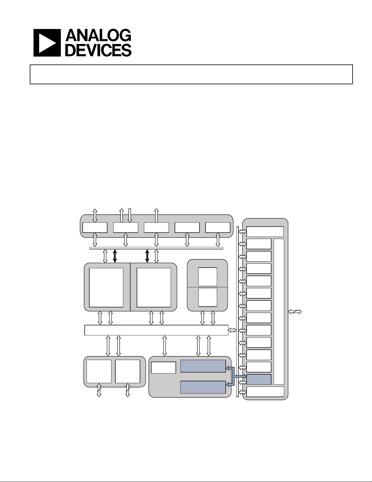
Dual-core symmetric high-performance Blackfin processor,
up to 500 MHz per core
Each core contains two 16-bit MACs, two 40-bit ALUs, and a
40-bit barrel shifter
RISC-like register and instruction model for ease of
programming and compiler-friendly support
Advanced debug, trace, and performance monitoring
Pipelined Vision Processor provides hardware to process sig-
nal and image algorithms used for pre- and co-processing
of video frames in ADAS or other video processing
applications
Accepts a range of supply voltages for I/O operation. See
Operating Conditions on Page 31
Off-chip voltage regulator interface
349-ball (19 mm × 19 mm) RoHS compliant BGA package
MEMORY
Each core contains 148K bytes of L1 SRAM memory (proces-
sor core-accessible) with multi-parity bit protection
Up to 256K bytes of L2 SRAM memory with ECC protection
Dynamic memory controller provides 16-bit interface to a
single bank of DDR2 or LPDDR DRAM devices
Static memory controller with asynchronous memory inter-
face that supports 8-bit and 16-bit memories
Flexible booting options from flash, eMMC and SPI memories
and from SPI, link port and UART hosts
Memory management unit provides memory protection
Blackfin and the Blackfin logo are registered trademarks of Analog Devices, Inc.
Rev. PrD
Information furnished by Analog Devices is believed to be accurate and reliable.
However, no responsibility is assumed by Analog Devices for its use, nor for any
infringements of patents or other rights of third parties that may result from its use.
Specifications subject to change without notice. No license is granted by implication
or otherwise under any patent or patent rights of Analog Devices. Trademarks and
registered trademarks are the property of their respective owners.
Figure 1. Processor Block Diagram
One Technology Way, P.O. Box 9106, Norwood, MA 02062-9106 U.S.A.
Tel: 781.329.4700 www.analog.com
Fax: 781.461.3113 © 2012 Analog Devices, Inc. All rights reserved.
Page 2

ADSP-BF606/ADSP-BF607/ADSP-BF608/ADSP-BF609 Preliminary Technical Data
TABLE OF CONTENTS
Features ................................................................. 1
Memory ................................................................ 1
General Description ................................................. 3
Blackfin Processor Core .......................................... 3
Instruction Set Description ..................................... 4
Processor Infrastructure ......................................... 5
Memory Architecture ............................................ 6
Video Subsystem .................................................. 9
Processor Safety Features ...................................... 10
Additional Processor Peripherals ............................ 11
Power and Clock Management ............................... 14
System Debug .................................................... 17
EZ-KIT Lite® Evaluation Board .............................. 17
Designing an Emulator-Compatible
Processor Board (Target) ................................... 17
Related Documents ............................................. 18
REVISION HISTORY
3/12—Revision PrD: Initial public version
Related Signal Chains ........................................... 18
Signal Descriptions ................................................. 19
Pin Multiplexing ................................................. 20
Pin Termination and Drive Characteristics-Requirements 24
Specifications ........................................................ 31
Operating Conditions ........................................... 31
Electrical Characteristics ....................................... 33
Processor — Absolute Maximum Ratings .................. 34
ESD Sensitivity ................................................... 34
Processor — Package Information ........................... 34
Environmental Conditions .................................... 35
349-Ball CSP_BGA Ball Assignments .......................... 36
Outline Dimensions ................................................ 42
Surface-Mount Design .......................................... 42
Automotive Products .............................................. 43
Pre Release Products ............................................... 43
Rev. PrD | Page 2 of 44 | March 2012
Page 3

Preliminary Technical Data
GENERAL DESCRIPTION
ADSP-BF606/ADSP-BF607/ADSP-BF608/ADSP-BF609
The ADSP-BF609 processor is a member of the Blackfin
family of products, incorporating the Analog Devices/Intel
Micro Signal Architecture (MSA). Blackfin processors combine
a dual-MAC state-of-the-art signal processing engine, the
advantages of a clean, orthogonal RISC-like microprocessor
instruction set, and single-instruction, multiple-data (SIMD)
multimedia capabilities into a single instruction-set
architecture.
The processor offers performance up to 500 MHz, as well as low
static power consumption. Produced with a low-power and lowvoltage design methodology, they provide world-class power
management and performance.
By integrating a rich set of industry-leading system peripherals
and memory (shown in Table 1), Blackfin processors are the
platform of choice for next-generation applications that require
RISC-like programmability, multimedia support, and leadingedge signal processing in one integrated package. These applications span a wide array of markets, from automotive systems to
embedded industrial, instrumentation and power/motor control applications.
Table 1. Processor Comparison
Processor Feature
ADSP-BF606
Up/Down/Rotary Counters 1
Timer/Counters with PWM 8
3-Phase PWM Units (4-pair) 2
SPORTs 3
SPIs 2
USB OTG 1
Parallel Peripheral Interface 3
Removable Storage Interface 1
CAN 1
TWI 2
UART 2
ADC Control Module (ACM) 1
Link Ports 4
Ethernet MAC (IEEE 1588) 2
Pixel Compositor (PIXC) No 1 1
Pipelined Vision Processor
1
(PVP)
GPIOs 112
ADSP-BF607
No VGA HD
ADSP-BF608
ADSP-BF609
Table 1. Processor Comparison (Continued)
Processor Feature
ADSP-BF606
L1 Instruction SRAM 64K
L1 Instruction SRAM/Cache 16K
L1 Data SRAM 32K
L1 Data SRAM/Cache 32K
L1 Scratchpad 4K
L2 Data SRAM 128K 256K
L2 Boot ROM 32K
Memory (bytes, per core)
Maximum Speed Grade (MHz)
Maximum SYSCLK (MHz)
Package Options 349-Ball CSP_BGA
1
VGA is 640 x 480 pixels per frame, 30 frames per second. HD is 1280 x 960 pixels
per frame, 30 frames per second.
2
Maximum speed grade is not available with every possible SYSCLK selection.
2
400
ADSP-BF607
250
ADSP-BF608
500
BLACKFIN PROCESSOR CORE
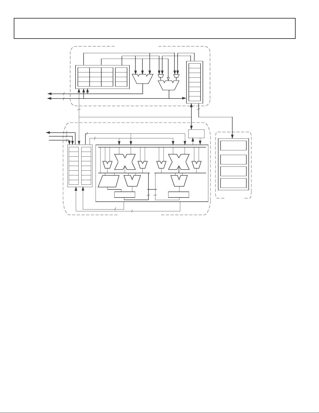
As shown in Figure 1, the processor integrates two Blackfin processor cores. Each core, shown in Figure 2, contains two 16-bit
multipliers, two 40-bit accumulators, two 40-bit ALUs, four
video ALUs, and a 40-bit shifter. The computation units process
8-, 16-, or 32-bit data from the register file.
The compute register file contains eight 32-bit registers. When
performing compute operations on 16-bit operand data, the
register file operates as 16 independent 16-bit registers. All
operands for compute operations come from the multiported
register file and instruction constant fields.
Each MAC can perform a 16-bit by 16-bit multiply in each
cycle, accumulating the results into the 40-bit accumulators.
Signed and unsigned formats, rounding, and saturation
are supported.
The ALUs perform a traditional set of arithmetic and logical
operations on 16-bit or 32-bit data. In addition, many special
instructions are included to accelerate various signal processing
tasks. These include bit operations such as field extract and population count, modulo 2
and rounding, and sign/exponent detection. The set of video
instructions include byte alignment and packing operations,
16-bit and 8-bit adds with clipping, 8-bit average operations,
and 8-bit subtract/absolute value/accumulate (SAA) operations.
Also provided are the compare/select and vector search
instructions.
For certain instructions, two 16-bit ALU operations can be performed simultaneously on register pairs (a 16-bit high half and
16-bit low half of a compute register). If the second ALU is used,
quad 16-bit operations are possible.
32
multiply, divide primitives, saturation
ADSP-BF609
Rev. PrD | Page 3 of 44 | March 2012
Page 4
ADSP-BF606/ADSP-BF607/ADSP-BF608/ADSP-BF609 Preliminary Technical Data
SEQUENCER
ALIGN
DECODE
LOOP BUFFER
16
16
8888
40 40
A0 A1
BARREL
SHIFTER
DATA ARITHMETIC UNIT
CONTROL
UNIT
R7.H
R6.H
R5.H
R4.H
R3.H
R2.H
R1.H
R0.H
R7.L
R6.L
R5.L
R4.L
R3.L
R2.L
R1.L
R0.L
AS TAT
40 40
32
32
32
32
32
32
32LD0
LD1
SD
DAG0
DAG1
ADDRESS ARITHMETIC UNIT
I3
I2
I1
I0
L3
L2
L1
L0
B3
B2
B1
B0
M3
M2
M1
M0
SP
FP
P5
P4
P3
P2
P1
P0
DA1
DA0
32
32
32
PREG
RAB
32
TO MEMORY
The 40-bit shifter can perform shifts and rotates and is used to
support normalization, field extract, and field deposit
instructions.
The program sequencer controls the flow of instruction execution, including instruction alignment and decoding. For
program flow control, the sequencer supports PC relative and
indirect conditional jumps (with static branch prediction), and
subroutine calls. Hardware supports zero-overhead looping.
The architecture is fully interlocked, meaning that the programmer need not manage the pipeline when executing instructions
with data dependencies.
The address arithmetic unit provides two addresses for simultaneous dual fetches from memory. It contains a multiported
register file consisting of four sets of 32-bit index, modify,
length, and base registers (for circular buffering), and eight
additional 32-bit pointer registers (for C-style indexed stack
manipulation).
Blackfin processors support a modified Harvard architecture in
combination with a hierarchical memory structure. Level 1 (L1)
memories are those that typically operate at the full processor
speed with little or no latency. At the L1 level, the instruction
memory holds instructions only. The data memory holds data,
and a dedicated scratchpad data memory stores stack and local
variable information.
Figure 2. Blackfin Processor Core
In addition, multiple L1 memory blocks are provided, offering a
configurable mix of SRAM and cache. The memory management unit (MMU) provides memory protection for individual
tasks that may be operating on the core and can protect system
registers from unintended access.
The architecture provides three modes of operation: user mode,
supervisor mode, and emulation mode. User mode has
restricted access to certain system resources, thus providing a
protected software environment, while supervisor mode has
unrestricted access to the system and core resources.
INSTRUCTION SET DESCRIPTION
The Blackfin processor instruction set has been optimized so
that 16-bit opcodes represent the most frequently used instructions, resulting in excellent compiled code density. Complex
DSP instructions are encoded into 32-bit opcodes, representing
fully featured multifunction instructions. Blackfin processors
support a limited multi-issue capability, where a 32-bit instruction can be issued in parallel with two 16-bit instructions,
allowing the programmer to use many of the core resources in a
single instruction cycle.
The Blackfin processor family assembly language instruction set
employs an algebraic syntax designed for ease of coding and
readability. The instructions have been specifically tuned to provide a flexible, densely encoded instruction set that compiles to
Rev. PrD | Page 4 of 44 | March 2012
Page 5

Preliminary Technical Data
ADSP-BF606/ADSP-BF607/ADSP-BF608/ADSP-BF609
a very small final memory size. The instruction set also provides
fully featured multifunction instructions that allow the programmer to use many of the processor core resources in a single
instruction. Coupled with many features more often seen on
microcontrollers, this instruction set is very efficient when compiling C and C++ source code. In addition, the architecture
supports both user (algorithm/application code) and supervisor
(O/S kernel, device drivers, debuggers, ISRs) modes of operation, allowing multiple levels of access to core
processor resources.
The assembly language, which takes advantage of the processor’s unique architecture, offers the following advantages:
• Seamlessly integrated DSP/MCU features are optimized for
both 8-bit and 16-bit operations.
• A multi-issue load/store modified-Harvard architecture,
which supports two 16-bit MAC or four 8-bit ALU + two
load/store + two pointer updates per cycle.
• All registers, I/O, and memory are mapped into a unified
4G byte memory space, providing a simplified programming model.
• Control of all asynchronous and synchronous events to the
processor is handled by two subsystems: the Core Event
Controller (CEC) and the System Event Controller (SEC).
• Microcontroller features, such as arbitrary bit and bit-field
manipulation, insertion, and extraction; integer operations
on 8-, 16-, and 32-bit data-types; and separate user and
supervisor stack pointers.
• Code density enhancements, which include intermixing of
16-bit and 32-bit instructions (no mode switching, no code
segregation). Frequently used instructions are encoded
in 16 bits.
PROCESSOR INFRASTRUCTURE
The following sections provide information on the primary
infrastructure components of the ADSP-BF609 processor.
DMA Controllers
The processor uses Direct Memory Access (DMA) to transfer
data within memory spaces or between a memory space and a
peripheral. The processor can specify data transfer operations
and return to normal processing while the fully integrated DMA
controller carries out the data transfers independent of processor activity.
DMA transfers can occur between memory and a peripheral or
between one memory and another memory. Two channels are
used for Memory-to-Memory DMA where one channel is the
source channel, and the second is the destination channel.
All DMAs can transport data to and from all on-chip and offchip memories. Programs can use two types of DMA transfers,
descriptor-based or register-based. Register-based DMA allows
the processor to directly program DMA control registers to initiate a DMA transfer. On completion, the control registers may
be automatically updated with their original setup values for
continuous transfer. Descriptor-based DMA transfers require a
set of parameters stored within memory to initiate a DMA
sequence. Descriptor-based DMA transfers allow multiple
DMA sequences to be chained together and a DMA channel can
be programmed to automatically set up and start another DMA
transfer after the current sequence completes.
The DMA controller supports the following DMA operations.
• A single linear buffer that stops on completion.
• A linear buffer with negative, positive or zero stride length.
• A circular, auto-refreshing buffer that interrupts when each
buffer becomes full.
• A similar buffer that interrupts on fractional buffers (for
example, 1/2, 1/4).
• 1D DMA – uses a set of identical ping-pong buffers defined
by a linked ring of two-word descriptor sets, each containing a link pointer and an address.
• 1D DMA – uses a linked list of 4 word descriptor sets containing a link pointer, an address, a length, and a
configuration.
• 2D DMA – uses an array of one-word descriptor sets, specifying only the base DMA address.
• 2D DMA – uses a linked list of multi-word descriptor sets,
specifying everything.
CRC Protection
The two CRC protection modules allow system software to periodically calculate the signature of code and/or data in memory,
the content of memory-mapped registers, or communication
message objects. Dedicated hardware circuitry compares the
signature with pre calculated values and triggers appropriate
fault events.
For example, every 100 ms the system software might initiate
the signature calculation of the entire memory contents and
compare these contents with expected, pre calculated values. If a
mismatch occurs, a fault condition can be generated (via the
processor core or the trigger routing unit).
The CRC is a hardware module based on a CRC32 engine that
computes the CRC value of the 32-bit data words presented to
it. Data is provided by the source channel of the memory-tomemory DMA (in memory scan mode) and is optionally forwarded to the destination channel (memory transfer mode).
The main features of the CRC peripheral are:
•Memory scan mode
•Memory transfer mode
•Data verify mode
• Data fill mode
• User-programmable CRC32 polynomial
• Bit/byte mirroring option (endianness)
• Fault/error interrupt mechanisms
• 1D and 2D fill block to initialize array with constants.
• 32-bit CRC signature of a block of a memory or MMR
block.
Rev. PrD | Page 5 of 44 | March 2012
Page 6

ADSP-BF606/ADSP-BF607/ADSP-BF608/ADSP-BF609 Preliminary Technical Data
Event Handling
The processor provides event handling that supports both nesting and prioritization. Nesting allows multiple event service
routines to be active simultaneously. Prioritization ensures that
servicing of a higher-priority event takes precedence over servicing of a lower-priority event. The processor provides support
for five different types of events:
• Emulation – An emulation event causes the processor to
enter emulation mode, allowing command and control of
the processor via the JTAG interface.
• Reset – This event resets the processor.
• Nonmaskable Interrupt (NMI) – The NMI event can be
generated either by the software watchdog timer, by the
input signal to the processor, or by software. The
NMI
NMI event is frequently used as a power-down indicator to
initiate an orderly shutdown of the system.
• Exceptions – Events that occur synchronously to program
flow (in other words, the exception is taken before the
instruction is allowed to complete). Conditions such as
data alignment violations and undefined instructions cause
exceptions.
• Interrupts – Events that occur asynchronously to program
flow. They are caused by input signals, timers, and other
peripherals, as well as by an explicit software instruction.
Core Event Controller (CEC)
The CEC supports nine general-purpose interrupts (IVG15–7),
in addition to the dedicated interrupt and exception events. Of
these general-purpose interrupts, the two lowest-priority
interrupts (IVG15–14) are recommended to be reserved for
software interrupt handlers. For more information, see the
ADSP-BF60x Processor Programmer’s Reference.
System Event Controller (SEC)
The SEC manages the enabling, prioritization, and routing of
events from each system interrupt or fault source. Additionally,
it provides notification and identification of the highest priority
active system interrupt request to each core and routes system
fault sources to its integrated fault management unit.
Trigger Routing Unit (TRU)
The TRU provides system-level sequence control without core
intervention. The TRU maps trigger masters (generators of triggers) to trigger slaves (receivers of triggers). Slave endpoints can
be configured to respond to triggers in various ways. Common
applications enabled by the TRU include:
• Automatically triggering the start of a DMA sequence after
a sequence from another DMA channel completes
•Software triggering
• Synchronization of concurrent activities
Pin Interrupts
Every port pin on the processor can request interrupts in either
an edge-sensitive or a level-sensitive manner with programmable polarity. Interrupt functionality is decoupled from GPIO
operation. Six system-level interrupt channels (PINT0–5) are
reserved for this purpose. Each of these interrupt channels can
manage up to 32 interrupt pins. The assignment from pin to
interrupt is not performed on a pin-by-pin basis. Rather, groups
of eight pins (half ports) can be flexibly assigned to interrupt
channels.
Every pin interrupt channel features a special set of 32-bit memory-mapped registers that enable half-port assignment and
interrupt management. This includes masking, identification,
and clearing of requests. These registers also enable access to the
respective pin states and use of the interrupt latches, regardless
of whether the interrupt is masked or not. Most control registers
feature multiple MMR address entries to write-one-to-set or
write-one-to-clear them individually.
General-Purpose I/O (GPIO)
Each general-purpose port pin can be individually controlled by
manipulation of the port control, status, and interrupt registers:
• GPIO direction control register – Specifies the direction of
each individual GPIO pin as input or output.
• GPIO control and status registers – A “write one to modify” mechanism allows any combination of individual
GPIO pins to be modified in a single instruction, without
affecting the level of any other GPIO pins.
• GPIO interrupt mask registers – Allow each individual
GPIO pin to function as an interrupt to the processor.
GPIO pins defined as inputs can be configured to generate
hardware interrupts, while output pins can be triggered by
software interrupts.
• GPIO interrupt sensitivity registers – Specify whether individual pins are level- or edge-sensitive and specify—if
edge-sensitive—whether just the rising edge or both the rising and falling edges of the signal are significant.
Pin Multiplexing
The processor supports a flexible multiplexing scheme that multiplexes the GPIO pins with various peripherals. A maximum of
4 peripherals plus GPIO functionality is shared by each GPIO
pin. All GPIO pins have a bypass path feature – that is, when the
output enable and the input enable of a GPIO pin are both
active, the data signal before the pad driver is looped back to the
receive path for the same GPIO pin. For more information, see
Pin Multiplexing on Page 20.
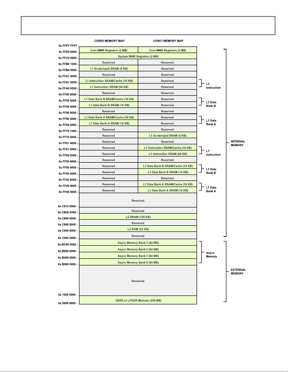
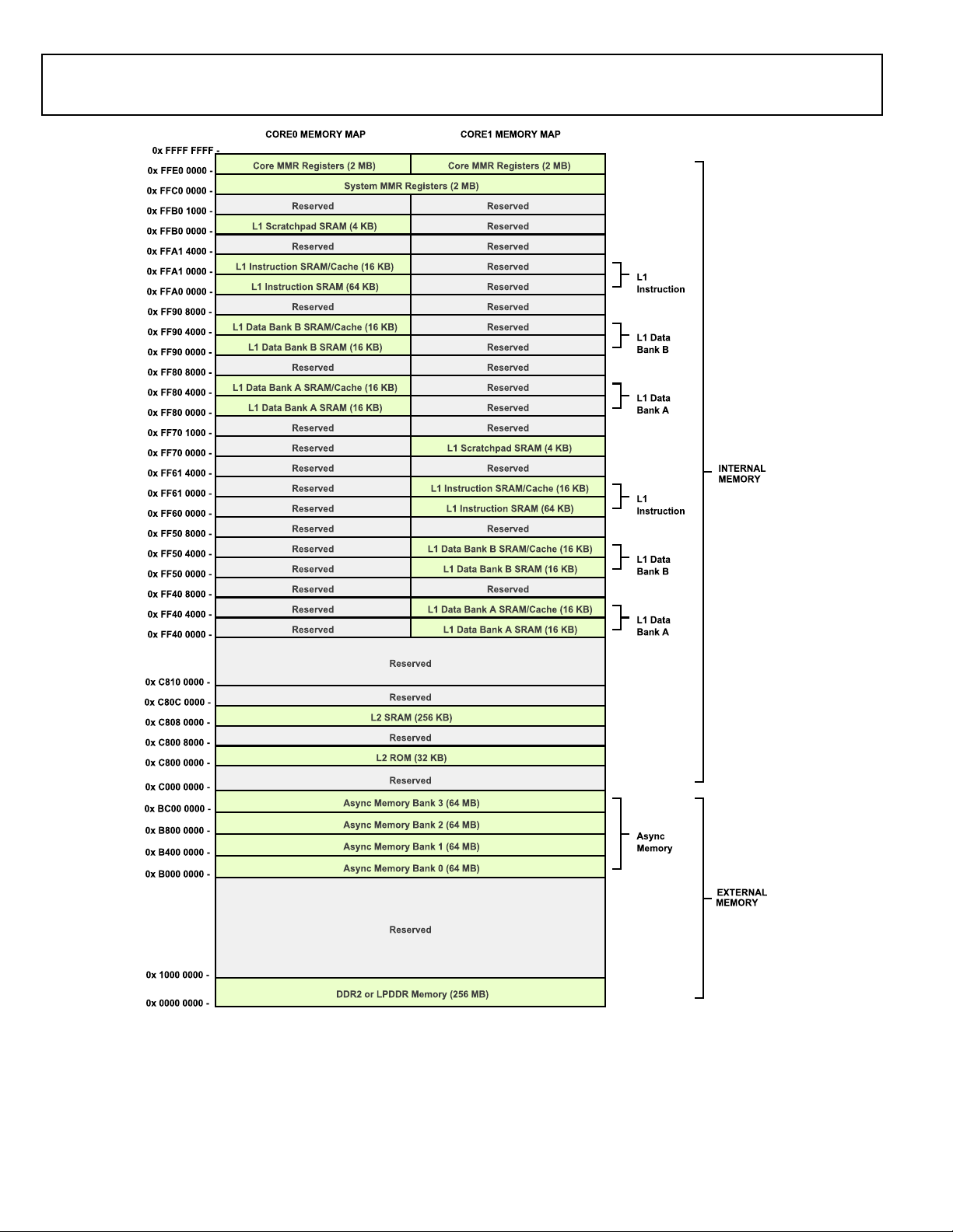
MEMORY ARCHITECTURE
The ADSP-BF609 processor views memory as a single unified
4G byte address space, using 32-bit addresses. All resources,
including internal memory, external memory, and I/O control
registers, occupy separate sections of this common address
space. The memory portions of this address space are arranged
in a hierarchical structure to provide a good cost/performance
balance of some very fast, low-latency core-accessible memory
as cache or SRAM, and larger, lower-cost and performance
interface-accessible memory systems. See Figure 3 and Figure 4.
Rev. PrD | Page 6 of 44 | March 2012
Page 7
Preliminary Technical Data
ADSP-BF606/ADSP-BF607/ADSP-BF608/ADSP-BF609
Figure 3. ADSP-BF606 Internal/External Memory Map
Rev. PrD | Page 7 of 44 | March 2012
Page 8
ADSP-BF606/ADSP-BF607/ADSP-BF608/ADSP-BF609 Preliminary Technical Data
Figure 4. ADSP-BF607/ADSP-BF608/ADSP-BF609 Internal/External Memory Map
Rev. PrD | Page 8 of 44 | March 2012
Page 9

Preliminary Technical Data
ADSP-BF606/ADSP-BF607/ADSP-BF608/ADSP-BF609
Internal (Core-Accessible) Memory
The L1 memory system is the highest-performance memory
available to the Blackfin processor cores.
Each core has its own private L1 memory. The modified Harvard architecture supports two concurrent 32-bit data accesses
along with an instruction fetch at full processor speed which
provides high bandwidth processor performance. Two separate
64K-byte of data memory blocks partner with an 80K-byte
memory block for instruction storage. Each block is multibanked for efficient data exchange through DMA and can be
configured as SRAM. Alternatively, 16K bytes of each block can
be configured in L1 cache mode. The four-way set-associative
instruction cache and the 2 two-way set-associative data caches
greatly accelerate memory access performance, especially when
accessing external memories.
The L1 memory domain also features a 4K-byte scratchpad
SRAM block which is ideal for storing local variables and the
software stack. All L1 memory is protected by a multi-parity bit
concept, regardless of whether the memory is operating in
SRAM or cache mode.
Outside of the L1 domain, L2 and L3 memories are arranged
using a Von Neumann topology. The L2 memory domain is a
unified instruction and data memory and can hold any mixture
of code and data required by the system design. The L2 memory
domain is accessible by both Blackfin cores through a dedicated
64-bit interface. It operates at half the frequency of the cores.
The processor features up to 256K bytes of L2 SRAM which is
ECC-protected and organized in eight banks. Individual banks
can be made private to any of the cores or the DMA subsystem.
There is also a 32K-byte single-bank ROM in the L2 domain. It
contains boot code and safety functions.
Static Memory Controller (SMC)
The SMC can be programmed to control up to four banks of
external memories or memory-mapped devices, with very flexible timing parameters. Each bank occupies a 64M byte segment
regardless of the size of the device used, so that these banks are
only contiguous if each is fully populated with 64M bytes of
memory.
Dynamic Memory Controller (DMC)
The DMC includes a controller that supports JESD79-2E compatible double data rate (DDR2) SDRAM and JESD209A low
power DDR (LPDDR) SDRAM devices.
I/O Memory Space
The processor does not define a separate I/O space. All
resources are mapped through the flat 32-bit address space. Onchip I/O devices have their control registers mapped into memory-mapped registers (MMRs) at addresses near the top of the
4G byte address space. These are separated into two smaller
blocks, one which contains the control MMRs for all core functions, and the other which contains the registers needed for
setup and control of the on-chip peripherals outside of the core.
The MMRs are accessible only in supervisor mode and appear
as reserved space to on-chip peripherals.
Booting
The processor has several mechanisms for automatically loading
internal and external memory after a reset. The boot mode is
defined by the SYS_BMODE input pins dedicated for this purpose. There are two categories of boot modes. In master boot
modes, the processor actively loads data from parallel or serial
memories. In slave boot modes, the processor receives data
from external host devices.
The boot modes are shown in Table 2. These modes are implemented by the SYS_BMODE bits of the reset configuration
register and are sampled during power-on resets and softwareinitiated resets.
Table 2. Boot Modes
SYS_BMODE Setting Boot Mode
000 No boot/Idle
001 Memory
010 RSI0 Master
011 SPI0 Master
100 SPI0 Slave
101 Reserved
110 LP0 Slave
111 UART0 Slave
VIDEO SUBSYSTEM
The following sections describe the components of the processor’s video subsystem. These blocks are shown with blue
shading in Figure 1 on Page 1.
Video Interconnect (VID)
The Video Interconnect provides a connectivity matrix that
interconnects the Video Subsystem: three PPIs, the PIXC, and
the PVP. The interconnect uses a protocol to manage data
transfer among these video peripherals.
Pipelined Vision Processor (PVP)
The PVP engine provides hardware implementation of signal
and image processing algorithms that are required for
co-processing and pre-processing of monochrome video frames
in ADAS applications, robotic systems, and other machine
applications.
The PVP works in conjunction with the Blackfin cores. It is
optimized for convolution and wavelet based object detection
and classification, and tracking and verification algorithms. The
PVP has the following processing blocks.
• Four 5x5 16-bit convolution blocks optionally followed by
down scaling
• A 16-bit cartesian-to-polar coordinate conversion block
• A pixel edge classifier that supports 1st and 2nd derivative
modes
• An arithmetic unit with 32-bit addition, multiply and
divide
Rev. PrD | Page 9 of 44 | March 2012
Page 10

ADSP-BF606/ADSP-BF607/ADSP-BF608/ADSP-BF609 Preliminary Technical Data
• A 32-bit threshold block with 16 thresholds, a histogram,
and run-length encoding
• Two 32-bit integral blocks that support regular and diagonal integrals
• An up- and down-scaling unit with independent scaling
ratios for horizontal and vertical components
• Input and output formatters for compatibility with many
data formats, including Bayer input format
The PVP can form a pipe of all the constituent algorithmic
modules and is dynamically reconfigurable to form different
pipeline structures.
The PVP supports the simultaneous processing of up to four
data streams. The memory pipe stream operates on data
received by DMA from any L1, L2, or L3 memory. The three
camera pipe streams operate on a common input received
directly from any of the three PPI inputs. Optionally, the PIXC
can convert color data received by the PPI and forward luma
values to the PVP’s monochrome engine. Each stream has a
dedicated DMA output. This preprocessing concept ensures
careful use of available power and bandwidth budgets and frees
up the processor cores for other tasks.
The PVP provides for direct core MMR access to all control/status registers. Two hardware interrupts interface to the system
event controller. For optimal performance, the PVP allows register programming through its control DMA interface, as well as
outputting selected status registers through the status DMA
interface. This mechanism enables the PVP to automatically
process job lists completely independent of the Blackfin cores.
Pixel Compositor (PIXC)
The pixel compositor (PIXC) provides image overlays with
transparent-color support, alpha blending, and color space conversion capabilities for output to TFT LCDs and NTSC/PAL
video encoders. It provides all of the control to allow two data
streams from two separate data buffers to be combined,
blended, and converted into appropriate forms for both LCD
panels and digital video outputs. The main image buffer provides the basic background image, which is presented in the
data stream. The overlay image buffer allows the user to add
multiple foreground text, graphics, or video objects on top of
the main image or video data stream.
Parallel Peripheral Interface (PPI)
The processor provides up to three parallel peripheral interfaces
(PPIs), supporting data widths up to 24 bits. The PPI supports
direct connection to TFT LCD panels, parallel analog-to-digital
and digital-to-analog converters, video encoders and decoders,
image sensor modules and other general-purpose peripherals.
The following features are supported in the PPI module:
• Programmable data length: 8 bits, 10 bits, 12 bits, 14 bits,
16 bits, 18 bits, and 24 bits per clock.
• Various framed, non-framed, and general-purpose operating modes. Frame syncs can be generated internally or can
be supplied by an external device.
• ITU-656 status word error detection and correction for
ITU-656 receive modes and ITU-656 preamble and status
word decode.
• Optional packing and unpacking of data to/from 32 bits
from/to 8 bits, 16 bits and 24 bits. If packing/unpacking is
enabled, endianness can be configured to change the order
of packing/unpacking of bytes/words.
• RGB888 can be converted to RGB666 or RGB565 for transmit modes.
•Various de-interleaving/interleaving modes for receiving/transmitting 4:2:2 YCrCb data.
•Configurable LCD data enable (DEN) output available on
Frame Sync 3.
PROCESSOR SAFETY FEATURES
The ADSP-BF609 processor has been designed for functional
safety applications. While the level of safety is mainly dominated by the system concept, the following primitives are
provided by the devices to build a robust safety concept.
Dual Core Supervision
The processor has been implemented as dual-core devices to
separate critical tasks to large independency. Software models
support mutual supervision of the cores in symmetrical fashion.
Multi-Parity-Bit-Protected L1 Memories
In the processor’s L1 memory space, whether SRAM or cache,
each word is protected by multiple parity bits to detect the single
event upsets that occur in all RAMs. This applies both to L1
instruction and data memory spaces.
ECC-Protected L2 Memories
Error correcting codes (ECC) are used to correct single event
upsets. The L2 memory is protected with a Single Error CorrectDouble Error Detect (SEC-DED) code. By default ECC is
enabled, but it can be disabled on a per-bank basis. Single-bit
errors are transparently corrected. Dual-bit errors can issue a
system event or fault if enabled. ECC protection is fully transparent to the user, even if L2 memory is read or written by 8-bit
or 16-bit entities.
CRC-Protected Memories
While parity bit and ECC protection mainly protect against random soft errors in L1 and L2 memory cells, the CRC engines can
be used to protect against systematic errors (pointer errors) and
static content (instruction code) of L1, L2 and even L3 memories (DDR2, LPDDR). The processors feature two CRC engines
which are embedded in the memory-to-memory DMA controllers. CRC check sums can be calculated or compared on the fly
during memory transfers, or one or multiple memory regions
can be continuously scrubbed by single DMA work unit as per
DMA descriptor chain instructions. The CRC engine also protects data loaded during the boot process.
Rev. PrD | Page 10 of 44 | March 2012
Page 11

Preliminary Technical Data
ADSP-BF606/ADSP-BF607/ADSP-BF608/ADSP-BF609
Memory Protection
The Blackfin cores feature a memory protection concept, which
grants data and/or instruction accesses from enabled memory
regions only. A supervisor mode vs. user mode programming
model supports dynamically varying access rights. Increased
flexibility in memory page size options supports a simple
method of static memory partitioning.
System Protection
All system resources and L2 memory banks can be controlled by
either the processor cores, memory-to-memory DMA, or the
system debug unit (SDU). A system protection unit (SPU)
enables write accesses to specific resources that are locked to
any of four masters: Core 0, Core 1, Memory DMA, and the System Debug Unit. System protection is enabled in greater
granularity for some modules (L2, SEC and GPIO controllers)
through a global lock concept.
Watchpoint Protection
The primary purpose of watchpoints and hardware breakpoints
is to serve emulator needs. When enabled, they signal an emulator event whenever user-defined system resources are accessed
or a core executes from user-defined addresses. Watchdog
events can be configured such that they signal the events to the
other Blackfin core or to the fault management unit.
Dual Watchdog
The two on-chip watchdog timers each may supervise one
Blackfin core.
Bandwidth Monitor
All DMA channels that operate in memory-to-memory mode
(Memory DMA, PVP Memory Pipe DMA, PIXC DMA) are
equipped with a bandwidth monitor mechanism. They can signal a system event or fault when transactions tend to starve
because system buses are fully loaded with higher-priority
traffic.
Signal Watchdogs
The eight general-purpose timers feature two new modes to
monitor off-chip signals. The Watchdog Period mode monitors
whether external signals toggle with a period within an expected
range. The Watchdog Width mode monitors whether the pulse
widths of external signals are in an expected range. Both modes
help to detect incorrect undesired toggling (or lack thereof) of
system-level signals.
Up/Down Count Mismatch Detection
The up/down counter can monitor external signal pairs, such as
request/grant strobes. If the edge count mismatch exceeds the
expected range, the up/down counter can flag this to the processor or to the fault management unit.
Fault Management
The fault management unit is part of the system event controller
(SEC). Any system event, whether a dual-bit uncorrectable ECC
error, or any peripheral status interrupt, can be defined as being
a “fault”. Additionally, the system events can be defined as an
interrupt to the cores. If defined as such, the SEC forwards the
event to the fault management unit which may automatically
reset the entire device for reboot, or simply toggle the
SYS_FAULT output pins to signal off-chip hardware. Optionally, the fault management unit can delay the action taken via a
keyed sequence, to provide a final chance for the Blackfin cores
to resolve the crisis and to prevent the fault action from being
taken.
ADDITIONAL PROCESSOR PERIPHERALS
The processor contains a rich set of peripherals connected to the
core via several high-bandwidth buses, providing flexibility in
system configuration as well as excellent overall system performance (see the block diagram on Page 1). The processors
contain high-speed serial and parallel ports, an interrupt controller for flexible management of interrupts from the on-chip
peripherals or external sources, and power management control
functions to tailor the performance and power characteristics of
the processor and system to many application scenarios.
The following sections describe additional peripherals that were
not described in the previous sections.
Timers
The processor includes several timers which are described in the
following sections.
General-Purpose Timers
There is one GP timer unit and it provides eight general-purpose programmable timers. Each timer has an external pin that
can be configured either as a pulse width modulator (PWM) or
timer output, as an input to clock the timer, or as a mechanism
for measuring pulse widths and periods of external events.
These timers can be synchronized to an external clock input on
the TMRx pins, an external clock TMRCLK input pin, or to the
internal SCLK0.
The timer units can be used in conjunction with the UARTs and
the CAN controller to measure the width of the pulses in the
data stream to provide a software auto-baud detect function for
the respective serial channels.
The timers can generate interrupts to the processor core, providing periodic events for synchronization to either the system
clock or to external signals. Timer events can also trigger other
peripherals via the TRU (for instance, to signal a fault).
Core Timers
Each processor core also has its own dedicated timer. This extra
timer is clocked by the internal processor clock and is typically
used as a system tick clock for generating periodic operating
system interrupts.
Watchd o g Ti m er s
Each core includes a 32-bit timer, which may be used to implement a software watchdog function. A software watchdog can
improve system availability by forcing the processor to a known
state, via generation of a hardware reset, nonmaskable interrupt
(NMI), or general-purpose interrupt, if the timer expires before
Rev. PrD | Page 11 of 44 | March 2012
Page 12
ADSP-BF606/ADSP-BF607/ADSP-BF608/ADSP-BF609 Preliminary Technical Data
SPORTx
SPT_AD1
SPT_AD0
SPT_CLK
SPT_FS
ADC
D
OUT
B
D
OUT
A
ADSCLK
CS
RANGE
SGL/DIFF
A[2:0]
ACM
ACM_FS
ACM_CLK
ACM_A4
ACM_A3
ACM_A[2:0]
ADSP-BF60x
SPORT
SELECT
MUX
being reset by software. The programmer initializes the count
value of the timer, enables the appropriate interrupt, then
enables the timer. Thereafter, the software must reload the
counter before it counts to zero from the programmed value.
This protects the system from remaining in an unknown state
where software, which would normally reset the timer, has
stopped running due to an external noise condition or software
error.
After a reset, software can determine if the watchdog was the
source of the hardware reset by interrogating a status bit in the
timer control register, which is set only upon a watchdog generated reset.
3-Phase PWM Units
The two 3-phase PWM generation units each feature:
• 16-bit center-based PWM generation unit
•Programmable PWM pulse width
• Single/double update modes
• Programmable dead time and switching frequency
• Twos-complement implementation which permits smooth
transition to full ON and full OFF states
• Dedicated asynchronous PWM shutdown signal
Each PWM block integrates a flexible and programmable
3-phase PWM waveform generator that can be programmed to
generate the required switching patterns to drive a 3-phase voltage source inverter for ac induction motor (ACIM) or
permanent magnet synchronous motor (PMSM) control. In
addition, the PWM block contains special functions that considerably simplify the generation of the required PWM
switching patterns for control of the electronically commutated
motor (ECM) or brushless dc motor (BDCM). Software can
enable a special mode for switched reluctance motors (SRM).
The eight PWM output signals (per PWM unit) consist of four
high-side drive signals and four low-side drive signals. The
polarity of a generated PWM signal can be set with software, so
that either active HI or active LO PWM patterns can be
produced.
Pulses synchronous to the switching frequency can be generated
internally and output on the PWM_SYNC pin. The PWM unit
can also accept externally generated synchronization pulses
through PWM_SYNC.
Each PWM unit features a dedicated asynchronous shutdown
pin which (when brought low) instantaneously places all six
PWM outputs in the OFF state.
Link Ports
Four DMA-enabled, 8-bit-wide link ports can connect to the
link ports of other DSPs or processors. Link ports are bidirectional ports having eight data lines, an acknowledge line and a
clock line.
Serial Ports (SPORTs)
Three synchronous serial ports that provide an inexpensive
interface to a wide variety of digital and mixed-signal peripheral
devices such as Analog Devices’ AD183x family of audio codecs,
ADCs, and DACs. The serial ports are made up of two data
lines, a clock, and frame sync. The data lines can be programmed to either transmit or receive and each data line has a
dedicated DMA channel.
Serial port data can be automatically transferred to and from
on-chip memory/external memory via dedicated DMA channels. Each of the serial ports can work in conjunction with
another serial port to provide TDM support. In this configuration, one SPORT provides two transmit signals while the other
SPORT provides the two receive signals. The frame sync and
clock are shared.
Serial ports operate in five modes:
• Standard DSP serial mode
•Multichannel (TDM) mode
2
S mode
•I
•Packed I
• Left-justified mode
ACM Interface
The ADC control module (ACM) provides an interface that
synchronizes the controls between the processor and an analogto-digital converter (ADC). The analog-to-digital conversions
are initiated by the processor, based on external or internal
events.
The ACM allows for flexible scheduling of sampling instants
and provides precise sampling signals to the ADC.
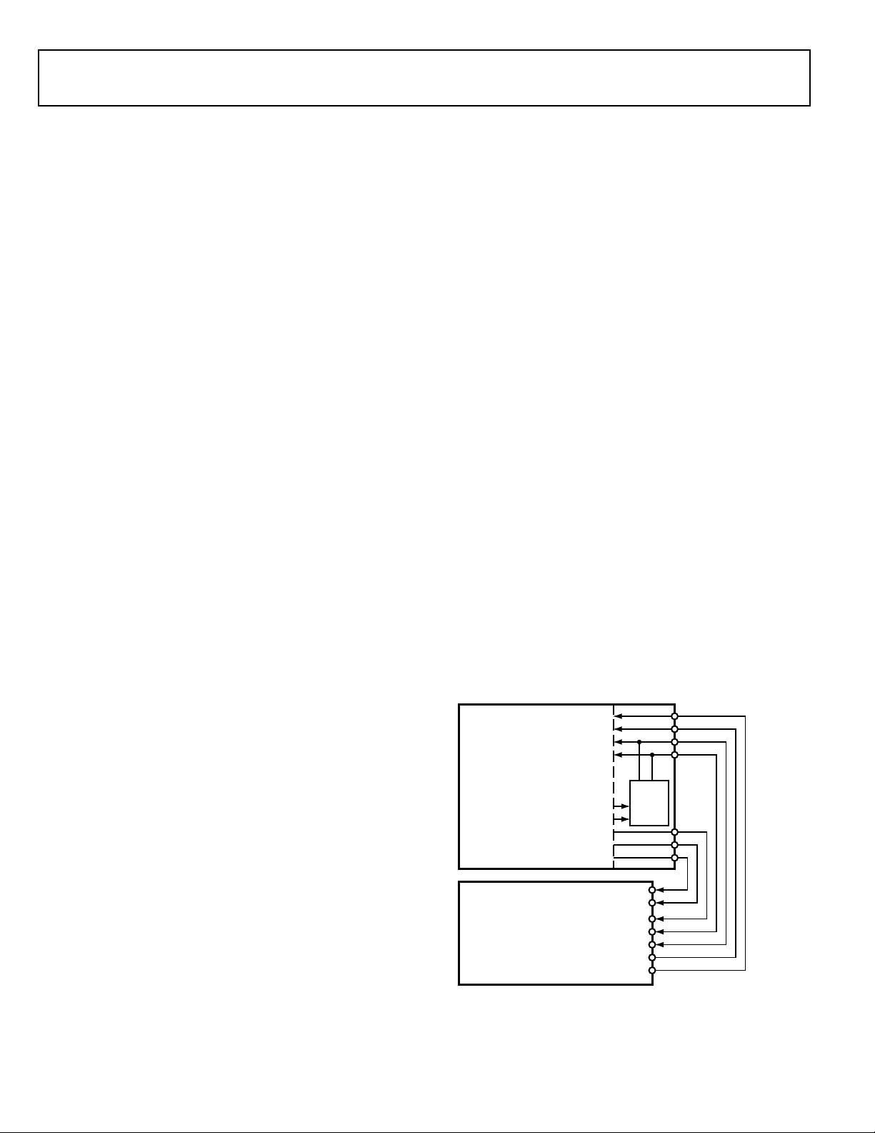
Figure 5 shows how to connect an external ADC to the ACM
and one of the SPORTs.
Rev. PrD | Page 12 of 44 | March 2012
2
S mode
Figure 5. ADC, ACM, and SPORT Connections
Page 13

Preliminary Technical Data
ADSP-BF606/ADSP-BF607/ADSP-BF608/ADSP-BF609
The ACM synchronizes the ADC conversion process, generating the ADC controls, the ADC conversion start signal, and
other signals. The actual data acquisition from the ADC is done
by a peripheral such as a SPORT or a SPI.
The processor interfaces directly to many ADCs without any
glue logic required.
General-Purpose Counters
A 32-bit counter is provided that can operate in general-purpose up/down count modes and can sense 2-bit quadrature or
binary codes as typically emitted by industrial drives or manual
thumbwheels. Count direction is either controlled by a levelsensitive input pin or by two edge detectors.
A third counter input can provide flexible zero marker support
and can alternatively be used to input the push-button signal of
thumb wheels. All three pins have a programmable debouncing
circuit.
Internal signals forwarded to each general-purpose timer enable
these timers to measure the intervals between count events.
Boundary registers enable auto-zero operation or simple system
warning by interrupts when programmable count values are
exceeded.
Serial Peripheral Interface (SPI) Ports
The processors have two SPI-compatible ports that allow the
processor to communicate with multiple SPI-compatible
devices.
In its simplest mode, the SPI interface uses three pins for transferring data: two data pins (Master Output-Slave Input, MOSI,
and Master Input-Slave Output, MISO) and a clock pin (serial
clock, SCK). An SPI chip select input pin (SPISS
devices select the processor, and seven SPI chip select output
pins (SPISEL7–1
SPI select pins are reconfigured general-purpose I/O pins. Using
these pins, the SPI port provides a full-duplex, synchronous
serial interface, which supports both master/slave modes and
multimaster environments.
The SPI port’s baud rate and clock phase/polarities are programmable, and it has integrated DMA channels for both
transmit and receive data streams.
) let the processor select other SPI devices. The
) lets other SPI
UART Ports
The processors provide two full-duplex universal asynchronous
receiver/transmitter (UART) ports, which are fully compatible
with PC-standard UARTs. Each UART port provides a simplified UART interface to other peripherals or hosts, supporting
full-duplex, DMA-supported, asynchronous transfers of serial
data. A UART port includes support for five to eight data bits,
and none, even, or odd parity. Optionally, an additional address
bit can be transferred to interrupt only addressed nodes in
multi-drop bus (MDB) systems. A frame is terminates by one,
one and a half, two or two and a half stop bits.
The UART ports support automatic hardware flow control
through the Clear To Send (CTS) input and Request To Send
(RTS) output with programmable assertion FIFO levels.
To help support the Local Interconnect Network (LIN) protocols, a special command causes the transmitter to queue a break
command of programmable bit length into the transmit buffer.
Similarly, the number of stop bits can be extended by a programmable inter-frame space.
The capabilities of the UARTs are further extended with support for the Infrared Data Association (IrDA®) serial infrared
physical layer link specification (SIR) protocol.
TWI Controller Interface
The processors include a 2-wire interface (TWI) module for
providing a simple exchange method of control data between
multiple devices. The TWI module is compatible with the
widely used I
capabilities of simultaneous master and slave operation and
support for both 7-bit addressing and multimedia data arbitration. The TWI interface utilizes two pins for transferring clock
(TWI_SCL) and data (TWI_SDA) and supports the protocol at
speeds up to 400k bits/sec. The TWI interface pins are compatible with 5 V logic levels.
Additionally, the TWI module is fully compatible with serial
camera control bus (SCCB) functionality for easier control of
various CMOS camera sensor devices.
2
C bus standard. The TWI module offers the
Removable Storage Interface (RSI)
The removable storage interface (RSI) controller acts as the host
interface for multimedia cards (MMC), secure digital memory
cards (SD), secure digital input/output cards (SDIO), and CEATA hard disk drives. The following list describes the main features of the RSI controller.
• Support for a single MMC, SD memory, SDIO card or CEATA hard disk drive
• Support for 1-bit and 4-bit SD modes
• Support for 1-bit, 4-bit, and 8-bit MMC modes
• Support for 4-bit and 8-bit CE-ATA hard disk drives
• Support for eMMC 4.3 embedded NAND flash devices
• A ten-signal external interface with clock, command, and
up to eight data lines
• Card interface clock generation from SCLK0
• SDIO interrupt and read wait features
• CE-ATA command completion signal recognition and
disable
Controller Area Network (CAN)
A CAN controller implements the CAN 2.0B (active) protocol.
This protocol is an asynchronous communications protocol
used in both industrial and automotive control systems. The
CAN protocol is well suited for control applications due to its
capability to communicate reliably over a network. This is
because the protocol incorporates CRC checking, message error
tracking, and fault node confinement.
Rev. PrD | Page 13 of 44 | March 2012
Page 14

ADSP-BF606/ADSP-BF607/ADSP-BF608/ADSP-BF609 Preliminary Technical Data
The CAN controller offers the following features:
• 32 mailboxes (8 receive only, 8 transmit only, 16 configurable for receive or transmit).
• Dedicated acceptance masks for each mailbox.
• Additional data filtering on first two bytes.
• Support for both the standard (11-bit) and extended (29bit) identifier (ID) message formats.
• Support for remote frames.
• Active or passive network support.
• CAN wakeup from hibernation mode (lowest static power
consumption mode).
• Interrupts, including: TX complete, RX complete, error
and global.
An additional crystal is not required to supply the CAN clock, as
the CAN clock is derived from a system clock through a programmable divider.
10/100 Ethernet MAC
The processor can directly connect to a network by way of an
embedded fast Ethernet media access controller (MAC) that
supports both 10-BaseT (10M bits/sec) and 100-BaseT (100M
bits/sec) operation. The 10/100 Ethernet MAC peripheral on the
processor is fully compliant to the IEEE 802.3-2002 standard
and it provides programmable features designed to minimize
supervision, bus use, or message processing by the rest of the
processor system.
Some standard features are:
• Support and RMII protocols for external PHYs
• Full duplex and half duplex modes
• Media access management (in half-duplex operation)
• Flow control
• Station management: generation of MDC/MDIO frames
for read-write access to PHY registers
Some advanced features are:
• Automatic checksum computation of IP header and IP
payload fields of Rx frames
• Independent 32-bit descriptor-driven receive and transmit
DMA channels
• Frame status delivery to memory through DMA, including
frame completion semaphores for efficient buffer queue
management in software
• Tx DMA support for separate descriptors for MAC header
and payload to eliminate buffer copy operations
• Convenient frame alignment modes
• 47 MAC management statistics counters with selectable
clear-on-read behavior and programmable interrupts on
half maximum value
• Advanced power management
• Magic packet detection and wakeup frame filtering
• Support for 802.3Q tagged VLAN frames
• Programmable MDC clock rate and preamble suppression
IEEE 1588 Support
The IEEE 1588 standard is a precision clock synchronization
protocol for networked measurement and control systems. The
processor includes hardware support for IEEE 1588 with an
integrated precision time protocol synchronization engine
(PTP_TSYNC). This engine provides hardware assisted time
stamping to improve the accuracy of clock synchronization
between PTP nodes. The main features of the engine are:
• Support for both IEEE 1588-2002 and IEEE 1588-2008 protocol standards
• Hardware assisted time stamping capable of up to 12.5 ns
resolution
• Lock adjustment
• Automatic detection of IPv4 and IPv6 packets, as well as
PTP messages
• Multiple input clock sources (SCLK0, RMII clock, external
clock)
• Programmable pulse per second (PPS) output
• Auxiliary snapshot to time stamp external events
USB 2.0 On-the-Go Dual-Role Device Controller
The USB 2.0 OTG dual-role device controller provides a lowcost connectivity solution for the growing adoption of this bus
standard in industrial applications, as well as consumer mobile
devices such as cell phones, digital still cameras, and MP3 players. The USB 2.0 controller allows these devices to transfer data
using a point-to-point USB connection without the need for a
PC host. The module can operate in a traditional USB peripheral-only mode as well as the host mode presented in the Onthe-Go (OTG) supplement to the USB 2.0 specification.
The USB clock (USB_CLKIN) is provided through a dedicated
external crystal or crystal oscillator.
The USB On-the-Go dual-role device controller includes a
Phase Locked Loop with programmable multipliers to generate
the necessary internal clocking frequency for USB.
POWER AND CLOCK MANAGEMENT
The processor provides four operating modes, each with a different performance/power profile. When configured for a 0 volt
internal supply voltage (V
nate state. Control of clocking to each of the processor
peripherals also reduces power consumption. See Table 5 for a
summary of the power settings for each mode.
Crystal Oscillator (SYS_XTAL)
The processor can be clocked by an external crystal, (Figure 6) a
sine wave input, or a buffered, shaped clock derived from an
external clock oscillator. If an external clock is used, it should be
a TTL compatible signal and must not be halted, changed, or
operated below the specified frequency during normal operation. This signal is connected to the processor’s SYS_CLKIN
), the processor enters the hiber-
DD_INT
Rev. PrD | Page 14 of 44 | March 2012
Page 15

Preliminary Technical Data
SYS_CLKIN
TO PLL
CIRCUITRY
FOR OVERTONE
OPERATION ONLY:
18 pF*
18 pF *
ȍ
*
BLACKFIN
ȍ
SYS_XTAL
TO USB PLL
BLACKFIN
ȍ
2
1, 2
NOTES:
1. CAPACITANCE VALUE SHOWN INCLUDES BOARD PARASITICS
2. VALUES ARE A PRELIMINARY ESTIMATE.
ADSP-BF606/ADSP-BF607/ADSP-BF608/ADSP-BF609
pin. When an external clock is used, the SYS_XTAL pin must be
left unconnected. Alternatively, because the processor includes
an on-chip oscillator circuit, an external crystal may be used.
NOTE: VALUES MARKED WITH * MUST BE CUSTOMIZED, DEPENDING
ON THE CRYSTAL AND LAYOUT. PLEASE ANALYZE CAREFULLY. FOR
FREQUENCIES ABOVE 33 MHz, THE SUGGESTED CAPACITOR VALUE
OF 18pF SHOULD BE TREATED AS A MAXIMUM, AND THE SUGGESTED
5(6,67259$/8(6+28/'%(5('8&('72ȍ
Figure 6. External Crystal Connection
For fundamental frequency operation, use the circuit shown in
Figure 6. A parallel-resonant, fundamental frequency, micro-
processor grade crystal is connected across the CLKIN and
XTAL pins. The on-chip resistance between CLKIN and the
XTAL pin is in the 500 kΩ range. Further parallel resistors are
typically not recommended.
The two capacitors and the series resistor shown in Figure 6 fine
tune phase and amplitude of the sine frequency. The capacitor
and resistor values shown in Figure 6 are typical values only.
The capacitor values are dependent upon the crystal manufacturers’ load capacitance recommendations and the PCB physical
layout. The resistor value depends on the drive level specified by
the crystal manufacturer. The user should verify the customized
values based on careful investigations on multiple devices over
temperature range.
A third-overtone crystal can be used for frequencies above
25 MHz. The circuit is then modified to ensure crystal operation
only at the third overtone by adding a tuned inductor circuit as
shown in Figure 6. A design procedure for third-overtone operation is discussed in detail in application note (EE-168) Using
Third Overtone Crystals with the ADSP-218x DSP on the Analog Devices website (www.analog.com)—use site search on
“EE-168.”
USB Crystal Oscillator
The USB can be clocked by an external crystal, a sine wave
input, or a buffered, shaped clock derived from an external
clock oscillator. If an external clock is used, it should be a TTL
compatible signal and must not be halted, changed, or operated
below the specified frequency during normal operation. This
signal is connected to the processor’s USB_XTAL pin. Alternatively, because the processor includes an on-chip oscillator
circuit, an external crystal may be used.
For fundamental frequency operation, use the circuit shown in
Figure 7. A parallel-resonant, fundamental frequency, micro-
processor grade crystal is connected between the USB_XTAL
pin and ground. A load capacitor is placed in parallel with the
crystal. The combined capacitive value of the board trace parasitic, the case capacitance of the crystal (from crystal
manufacturer) and the parallel capacitor in the diagram should
be in the range of 8 pF to 15 pF.
5-12 pf
Figure 7. External USB Crystal Connection
The crystal should be chosen so that its rated load capacitance
matches the nominal total capacitance on this node. A series
resistor may be added between the USB_XTAL pin and the parallel crystal and capacitor combination, in order to further
reduce the drive level of the crystal.
The parallel capacitor and the series resistor shown in Figure 7
fine tune phase and amplitude of the sine frequency. The capacitor and resistor values shown in Figure 7 are typical values
only. The capacitor values are dependent upon the crystal manufacturers’ load capacitance recommendations and the PCB
physical layout. The resistor value depends on the drive level
specified by the crystal manufacturer. The user should verify the
customized values based on careful investigations on multiple
devices over temperature range.
Clock Generation
The clock generation unit (CGU) generates all on-chip clocks
and synchronization signals. Multiplication factors are programmed to the PLL to define the PLLCLK frequency.
Programmable values divide the PLLCLK frequency to generate
the core clock (CCLK), the system clocks (SYSCLK, SCLK0 and
SCLK1), the LPDDR or DDR2 clock (DCLK) and the output
clock (OCLK). This is illustrated in Figure 8 on Page 32.
Writing to the CGU control registers does not affect the behavior of the PLL immediately. Registers are first programmed with
a new value, and the PLL logic executes the changes so that it
transitions smoothly from the current conditions to the new
ones.
SYS_CLKIN oscillations start when power is applied to the
pins. The rising edge of SYS_HWRST can be applied
V
DD_EXT
after all voltage supplies are within specifications (see Operating
Conditions on Page 31), and SYS_CLKIN oscillations are stable.
Rev. PrD | Page 15 of 44 | March 2012
Page 16

ADSP-BF606/ADSP-BF607/ADSP-BF608/ADSP-BF609 Preliminary Technical Data
Clock Out/External Clock
The SYS_CLKOUT output pin has programmable options to
output divided-down versions of the on-chip clocks, including
USB clocks. Note that the USBCLK is provided for debug purposes only and is not supported or guaranteed for clocking
customer applications. By default, the SYS_CLKOUT pin drives
a buffered version of the SYS_CLKIN input. Clock generation
faults (for example PLL unlock) may trigger a reset by hardware.
The clocks shown in Table 3 can be outputs from
SYS_CLKOUT.
Table 3. Clock Dividers
Clock Source Divider
CCLK (core clock) By 4
SYSCLK (System clock) By 2
SCLK0 (system clock for PVP, all
peripherals not covered by
SCLK1)
SCLK1 (system clock for SPORTS,
SPI, ACM)
DCLK (LPDDR/DDR2 clock) By 2
OCLK (output clock) Programmable
USBCLK None
CLKBUF None, direct from SYS_CLKIN
USBCLKBUF None, direct from USB_CLKIN
None
None
Power Management
As shown in Table 4, the processor supports five different power
domains, which maximizes flexibility while maintaining compliance with industry standards and conventions. There are no
sequencing requirements for the various power domains, but all
domains must be powered according to the appropriate Specifi-
cations table for processor operating conditions; even if the
feature/peripheral is not used.
Table 4. Power Domains
Power Domain VDD Range
All internal logic V
DDR2/LPDDR V
USB V
Thermal diode V
All other I/O (includes SYS, JTAG, and Ports pins) V
DD_INT
DD_DMC
DD_USB
DD_TD
DD_EXT
The dynamic power management feature of the processor
allows the processor’s core clock frequency (f
) to be dynam-
CCLK
ically controlled.
The power dissipated by a processor is largely a function of its
clock frequency and the square of the operating voltage. For
example, reducing the clock frequency by 25% results in a 25%
reduction in dynamic power dissipation.
Full-On Operating Mode—Maximum Performance
In the full-on mode, the PLL is enabled and is not bypassed,
providing capability for maximum operational frequency. This
is the power-up default execution state in which maximum performance can be achieved. The processor cores and all enabled
peripherals run at full speed.
Active Operating Mode—Moderate Dynamic Power Savings
In the active mode, the PLL is enabled but bypassed. Because the
PLL is bypassed, the processor’s core clocks and system clocks
run at the input clock (SYS_CLKIN) frequency. DMA access is
available to appropriately configured L1 memories.
For more information about PLL controls, see the “Dynamic
Power Management” chapter in the ADSP-BF60x Blackfin Pro-
cessor Hardware Reference.
See Table 5 for a summary of the power settings for each mode.
Table 5. Power Settings
f
,
SYSCLK
,
f
DCLK
PLL
Mode/State PLL
Full On Enabled No Enabled Enabled On
Active Enabled/
Disabled
Deep Sleep Disabled — Disabled Disabled On
Hibernate Disabled — Disabled Disabled Off
Bypassed f
Yes E nab le d E na bl ed On
CCLK
f
SCLK0
f
SCLK1
,
Core
Power
Deep Sleep Operating Mode—Maximum Dynamic Power
Savings
The deep sleep mode maximizes dynamic power savings by disabling the clocks to the processor core and to all synchronous
peripherals. Asynchronous peripherals may still be running but
cannot access internal resources or external memory.
Hibernate State—Maximum Static Power Savings
The hibernate state maximizes static power savings by disabling
the voltage and clocks to the processor cores and to all of the
peripherals. This setting signals the external voltage regulator
supplying the V
pins to shut off using the
DD_INT
SYS_EXTWAKE signal, which provides the lowest static power
dissipation. Any critical information stored internally (for
example, memory contents, register contents, and other information) must be written to a non-volatile storage device prior to
removing power if the processor state is to be preserved.
Since the V
pins can still be supplied in this mode, all of
DD_EXT
the external pins three-state, unless otherwise specified. This
allows other devices that may be connected to the processor to
still have power applied without drawing unwanted current.
Reset Control Unit
Reset is the initial state of the whole processor or one of the
cores and is the result of a hardware or software triggered event.
In this state, all control registers are set to their default values
Rev. PrD | Page 16 of 44 | March 2012
Page 17

Preliminary Technical Data
ADSP-BF606/ADSP-BF607/ADSP-BF608/ADSP-BF609
and functional units are idle. Exiting a full system reset starts
with Core-0 only being ready to boot. Exiting a Core-n only
reset starts with this Core-n being ready to boot.
The Reset Control Unit (RCU) controls how all the functional
units enter and exit reset. Differences in functional requirements and clocking constraints define how reset signals are
generated. Programs must guarantee that none of the reset
functions puts the system into an undefined state or causes
resources to stall. This is particularly important when only one
of the cores is reset (programs must ensure that there is no
pending system activity involving the core that is being reset).
From a system perspective reset is defined by both the reset target and the reset source as described below.
Target defined:
• Hardware Reset – All functional units are set to their
default states without exception. History is lost.
• System Reset – All functional units except the RCU are set
to their default states.
• Core-n only Reset – Affects Core-n only. The system software should guarantee that the core in reset state is not
accessed by any bus master.
Source defined:
• Hardware Reset – The SYS_HWRST
asserted active (pulled down).
• System Reset – May be triggered by software (writing to the
RCU_CTL register) or by another functional unit such as
the dynamic power management (DPM) unit (Hibernate)
or any of the system event controller (SEC), trigger routing
unit (TRU), or emulator inputs.
• Core-n-only reset – Triggered by software.
• Trigger request (peripheral).
input signal is
Voltage Regulation
The processor requires an external voltage regulator to power
the V
external voltage regulator can be signaled through
SYS_EXTWAKE to remove power from the processor core.
This signal is high-true for power-up and may be connected
directly to the low-true shut-down input of many common
regulators.
While in the hibernate state, all external supply pins (V
V
DD_USB
external buffers. The external voltage regulator can be activated
from this power down state by asserting the SYS_HWRST
which then initiates a boot sequence. SYS_EXTWAKE indicates
a wakeup to the external voltage regulator.
pins. To reduce standby power consumption, the
DD_INT
, V
) can still be powered, eliminating the need for
DD_DMC
DD_EXT
pin,
,
System Watchpoint Unit
The System Watchpoint Unit (SWU) is a single module which
connects to a single system bus and provides for transaction
monitoring. One SWU is attached to the bus going to each system slave. The SWU provides ports for all system bus address
channel signals. Each SWU contains four match groups of registers with associated hardware. These four SWU match groups
operate independently, but share common event (interrupt,
trigger and others) outputs.
System Debug Unit
The System Debug Unit (SDU) provides IEEE-1149.1 support
through its JTAG interface. In addition to traditional JTAG features, present in legacy Blackfin products, the SDU adds more
features for debugging the chip without halting the core
processors.
EZ-KIT LITE® EVALUATION BOARD
For evaluation of ADSP-BF606/ADSP-BF607/ADSPBF608/ADSP-BF609 processors, use the EZ-KIT Lite
available from Analog Devices. Order using part numbers
ADZS-BF609-EZLITE. The boards come with on-chip emulation capabilities and are equipped to enable software
development. Multiple daughter cards are available.
®
boards
DESIGNING AN EMULATOR-COMPATIBLE PROCESSOR BOARD (TARGET)
The Analog Devices family of emulators are tools that every system developer needs in order to test and debug hardware and
software systems. Analog Devices has supplied an IEEE 1149.1
JTAG Test Access Port (TAP) on each processor. The emulator
uses the TAP to access the internal features of the processor,
allowing the developer to load code, set breakpoints, observe
variables, observe memory, and examine registers. The processor must be halted to send data and commands, but once an
operation has been completed by the emulator, the processor
system is set running at full speed with no impact on
system timing.
To use these emulators, the target board must include a header
that connects the processor’s JTAG port to the emulator.
For details on target board design issues including mechanical
layout, single processor connections, multiprocessor scan
chains, signal buffering, signal termination, and emulator pod
logic, see (EE-68) Analog Devices JTAG Emulation Technical
Reference on the Analog Devices website (www.analog.com)—
use site search on “EE-68.” This document is updated regularly
to keep pace with improvements to emulator support.
SYSTEM DEBUG
The processor includes various features that allow for easy system debug. These are described in the following sections.
Rev. PrD | Page 17 of 44 | March 2012
Page 18

ADSP-BF606/ADSP-BF607/ADSP-BF608/ADSP-BF609 Preliminary Technical Data
RELATED DOCUMENTS
The following publications that describe the ADSPBF606/ADSP-BF607/ADSP-BF608/ADSP-BF609 processors
(and related processors) can be ordered from any Analog
Devices sales office or accessed electronically on our website:
• Getting Started With Blackfin Processors
• ADSP-BF606/ADSP-BF607/ADSP-BF608/ADSP-BF609
Blackfin Processor Hardware Reference
• Blackfin Processor Programming Reference
RELATED SIGNAL CHAINS
A signal chain is a series of signal-conditioning electronic components that receive input (data acquired from sampling either
real-time phenomena or from stored data) in tandem, with the
output of one portion of the chain supplying input to the next.
Signal chains are often used in signal processing applications to
gather and process data or to apply system controls based on
analysis of real-time phenomena. For more information about
this term and related topics, see the “signal chain” entry in the
Glossary of EE Terms on the Analog Devices website.
Analog Devices eases signal processing system development by
providing signal processing components that are designed to
work together well. A tool for viewing relationships between
specific applications and related components is available on the
www.analog.com website.
The Application Signal Chains page in the Circuits from the
TM
site (http:\\www.analog.com\circuits) provides:
Lab
• Graphical circuit block diagram presentation of signal
chains for a variety of circuit types and applications
• Drill down links for components in each chain to selection
guides and application information
• Reference designs applying best practice design techniques
Rev. PrD | Page 18 of 44 | March 2012
Page 19

Preliminary Technical Data
ADSP-BF606/ADSP-BF607/ADSP-BF608/ADSP-BF609
SIGNAL DESCRIPTIONS
The processors’ signal definitions are shown in Table 6.
Table 6. Processor Signal Descriptions
Signal Name Function Driver Type Power Domain
Ports Pins
PA00 – PA15 Port A 00 – Port A 15 A V
PB00 – PB15 Port B 00 – Port B 15 A V
PC00 – PC15 Port C 00 – Port C 15 A V
PD00 – PD15 Port D 00 – Port D 15 A V
PE00 – PE15 Port E 00 – Port E 15 A V
PF00 – PF15 Port F 00 – Port F 15 A V
PG00 – PG15 Port G 00 – Port G 15 A V
Dynamic Memory Controller
DMC0_A00 – DMC0_A13 DMC0 Address 0 – DMC0 Address 13 B V
DMC0_BA0 DMC0 Bank Address Input 0 B V
DMC0_BA1 DMC0 Bank Address Input 1 B V
DMC0_BA2 DMC0 Bank Address Input 2 B V
DMC0_CAS DMC0 Column Address Strobe B V
DMC0_CK DMC0 Clock C V
DMC0_CK DMC0 Clock (complement) C V
DMC0_CKE DMC0 Clock enable B V
DMC0_CS0 DMC0 Chip Select 0 B V
DMC0_DQ00 – DMC0_DQ15 DMC0 Data 0 – DMC0 Data 15 B V
DMC0_LDM DMC0 Data Mask for Lower Byte B V
DMC0_LDQS DMC0 Data Strobe for Lower Byte C V
DMC0_LDQS DMC0 Data Strobe for Lower Byte (complement) C V
DMC0_ODT DMC0 On-die termination B V
DMC0_RAS DMC0 Row Address Strobe B V
DMC0_UDM DMC0 Data Mask for Upper Byte B V
DMC0_UDQS DMC0 Data Strobe for Upper Byte C V
DMC0_UDQS DMC0 Data Strobe for Upper Byte (complement) C V
DMC0_WE DMC0 Write Enable B V
JTAG Test Access Port
JTG_EMU
JTG Emulation Output A V
JTG_TCK JTG Clock V
JTG_TDI JTG Serial Data In V
JTG_TDO JTG Serial Data Out A V
JTG_TMS JTG Mode Select V
JTG_TRST JTG Reset V
Static Memory Controller
SMC0_A01 SMC0 Address 1 A V
SMC0_A02 SMC0 Address 2 A V
SMC0_AMS0 SMC0 Memory Select 0 A V
SMC0_AOE/SMC0_NORDV SMC0 Output Enable/SMC0 NOR Data Valid A V
SMC0_ARDY/SMC0_NORWT SMC0 Asynchronous Ready/SMC0 NOR Wait V
SMC0_ARE SMC0 Read Enable A V
SMC0_AWE SMC0 Write Enable A V
SMC0_BR SMC0 Bus Request V
SMC0_D00 – SMC0_D15 SMC0 Data 0 – SMC0 Data 15 A V
DD_EXT
DD_EXT
DD_EXT
DD_EXT
DD_EXT
DD_EXT
DD_EXT
DD_DMC
DD_DMC
DD_DMC
DD_DMC
DD_DMC
DD_DMC
DD_DMC
DD_DMC
DD_DMC
DD_DMC
DD_DMC
DD_DMC
DD_DMC
DD_DMC
DD_DMC
DD_DMC
DD_DMC
DD_DMC
DD_DMC
DD_EXT
DD_EXT
DD_EXT
DD_EXT
DD_EXT
DD_EXT
DD_EXT
DD_EXT
DD_EXT
DD_EXT
DD_EXT
DD_EXT
DD_EXT
DD_EXT
DD_EXT
Rev. PrD | Page 19 of 44 | March 2012
Page 20

ADSP-BF606/ADSP-BF607/ADSP-BF608/ADSP-BF609 Preliminary Technical Data
Table 6. Processor Signal Descriptions (Continued)
Signal Name Function Driver Type Power Domain
System Booting, Clocking and Control
SYS_BMODE0 SYS Boot Mode Control 0 V
SYS_BMODE1 SYS Boot Mode Control 1 V
SYS_BMODE2 SYS Boot Mode Control 2 V
SYS_CLKIN SYS Clock/Crystal Input V
SYS_CLKOUT SYS Processor Clock Output A V
SYS_EXTWAKE SYS External Wake Control A V
SYS_FAULT SYS Fault Output A V
SYS_FAULT SYS Complementary Fault Output A V
SYS_NMI/SYS_RESOUT SYS Non-maskable Interrupt/SYS Reset Output A V
SYS_PWRGD SYS Power Good Indicator V
SYS_HWRST SYS Processor Reset Control V
SYS_TDA SYS Thermal Diode Anode V
SYS_TDK SYS Thermal Diode Cathode V
SYS_XTAL SYS Crystal Output V
2-Wire Interface
TWI0_SCL TWI0 Serial Clock D V
TWI0_SDA TWI0 Serial Data D V
TWI1_SCL TWI1 Serial Clock D V
TWI1_SDA TWI1 Serial Data D V
Universal Serial Bus
USB0_CLKIN USB0 Clock/Crystal Input V
USB0_DM USB0 Data – V
USB0_DP USB0 Data + V
USB0_ID USB0 OTG ID V
USB0_VBC USB0 VBUS Control V
USB0_VBUS USB0 Bus Voltage V
DD_EXT
DD_EXT
DD_EXT
DD_EXT
DD_EXT
DD_EXT
DD_EXT
DD_EXT
DD_EXT
DD_EXT
DD_EXT
DD_THD
DD_THD
DD_EXT
DD_EXT
DD_EXT
DD_EXT
DD_EXT
DD_USB
DD_USB
DD_USB
DD_USB
DD_USB
DD_USB
PIN MULTIPLEXING
In Table 7, the default state is shown in plain text, while the
alternate functions are shown in italics.
Table 7. Processor Multiplexing Scheme
Signal Name Function
Port A
PA _0 0/ SMC0_A03/EPPI2_D00/LP0_D0 PA Position 0/SMC0 Address 3/EPPI2 Data 0/LP0 Data 0
PA _0 1/ SMC0_A04/EPPI2_D01/LP0_D1 PA Position 1/SMC0 Address 4/EPPI2 Data 1/LP0 Data 1
PA _0 2/ SMC0_A05/EPPI2_D02/LP0_D2 PA Position 2/SMC0 Address 5/EPPI2 Data 2/LP0 Data 2
PA _0 3/ SMC0_A06/EPPI2_D03/LP0_D3 PA Position 3/SMC0 Address 6/EPPI2 Data 3/LP0 Data 3
PA _0 4/ SMC0_A07/EPPI2_D04/LP0_D4 PA Position 4/SMC0 Address 7/EPPI2 Data 4/LP0 Data 4
PA _0 5/ SMC0_A08/EPPI2_D05/LP0_D5 PA Position 5/SMC0 Address 8/EPPI2 Data 5/LP0 Data 5
PA _0 6/ SMC0_A09/EPPI2_D06/LP0_D6 PA Position 6/SMC0 Address 9/EPPI2 Data 6/LP0 Data 6
PA _0 7/ SMC0_A10/EPPI2_D07/LP0_D7 PA Position 7/SMC0 Address 10/EPPI2 Data 7/LP0 Data 7
PA _0 8/ SMC0_A11/EPPI2_D08/LP1_D0 PA Position 8/SMC0 Address 11/EPPI2 Data 8/LP1 Data 0
PA _0 9/ SMC0_A12/EPPI2_D09/LP1_D1 PA Position 9/SMC0 Address 12/EPPI2 Data 9/LP1 Data 1
PA _1 0/ SMC0_A14/EPPI2_D10/LP1_D2 PA Position 10/SMC0 Address 14/EPPI2 Data 10/LP1 Data 2
PA _1 1/ SMC0_A15/EPPI2_D11/LP1_D3 PA Position 11/SMC0 Address 15/EPPI2 Data 11/LP1 Data 3
PA _1 2/ SMC0_A17/EPPI2_D12/LP1_D4 PA Position 12/SMC0 Address 17/EPPI2 Data 12/LP1 Data 4
PA _1 3/ SMC0_A18/EPPI2_D13/LP1_D5 PA Position 13/SMC0 Address 18/EPPI2 Data 13/LP1 Data 5
Rev. PrD | Page 20 of 44 | March 2012
Page 21

Preliminary Technical Data
ADSP-BF606/ADSP-BF607/ADSP-BF608/ADSP-BF609
Table 7. Processor Multiplexing Scheme (Continued)
Signal Name Function
PA _1 4/ SMC0_A19/EPPI2_D14/LP1_D6 PA Position 14/SMC0 Address 19/EPPI2 Data 14/LP1 Data 6
PA _1 5/ SMC0_A20/EPPI2_D15/LP1_D7 PA Position 15/SMC0 Address 20/EPPI2 Data 15/LP1 Data 7
Port B
PB_00/SMC0_NORCLK/EPPI2_CLK/LP0_CLK PB Position 0/SMC0 NOR Clock/EPPI2 Clock/LP0 Clock
PB_01/SMC0_AMS1
PB_02/SMC0_A13/EPPI2_FS2/LP1_ACK PB Position 2/SMC0 Address 13/EPPI2 Frame Sync 2 (VSYNC)/LP1 Acknowledge
PB_03/SMC0_A16/EPPI2_FS3/LP1_CLK PB Position 3/SMC0 Address 16/EPPI2 Frame Sync 3 (FIELD)/LP1 Clock
PB_04/SMC0_AMS2
PB_05/SMC0_AMS3
PB_06/SMC0_A21/SPT0_ATDV/TM0_ACLK4 PB Position 6/SMC0 Address 21/SPORT0 Channel A Transmit Data Valid/
PB_07/SMC0_A22/EPPI2_D16/SPT0_BFS PB Position 7/SMC0 Address 22/EPPI2 Data 16/SPORT0 Channel B Frame Sync
PB_08/SMC0_A23/EPPI2_D17/SPT0_BCLK PB Position 8/SMC0 Address 23/EPPI2 Data 17/SPORT0 Channel B Clock
PB_09/SMC0_BGH
PB_10/SMC0_A24/SPT0_BD1/TM0_ACLK0 PB Position 10/SMC0 Address 24/SPORT0 Channel B Data 1/TIMER0 Alternate Clock 0
PB_11/SMC0_A25/SPT0_BD0/TM0_ACLK3 PB Position 11/SMC0 Address 25/SPORT0 Channel B Data 0/TIMER0 Alternate Clock 3
PB_12/SMC0_BG
TM0_ACLK1
PB_13/ETH0_TXEN/EPPI1_FS1/TM0_ACI6 PB Position 13/ETH0 Transmit Enable/EPPI1 Frame Sync 1 (HSYNC)/
PB_14/ETH0_REFCLK/EPPI1_CLK PB Position 14/ETH0 Reference Clock/EPPI1 Clock
PB_15/ETH0_PTPPPS/EPPI1_FS3 PB Position 15/ETH0 PTP Pulse-Per-Second Output/EPPI1 Frame Sync 3 (FIELD)
Port C
PC_00/ETH0_RXD0/EPPI1_D00 PC Position 0/ETH0 Receive Data 0/EPPI1 Data 0
PC_01/ETH0_RXD1/EPPI1_D01 PC Position 1/ETH0 Receive Data 1/EPPI1 Data 1
PC_02/ETH0_TXD0/EPPI1_D02 PC Position 2/ETH0 Transmit Data 0/EPPI1 Data 2
PC_03/ETH0_TXD1/EPPI1_D03 PC Position 3/ETH0 Transmit Data 1/EPPI1 Data 3
PC_04/ETH0_RXERR/EPPI1_D04 PC Position 4/ETH0 Receive Error/EPPI1 Data 4
PC_05/ETH0_CRS/EPPI1_D05 PC Position 5/ETH0 Carrier Sense/RMII Receive Data Valid/EPPI1 Data 5
PC_06/ETH0_MDC/EPPI1_D06 PC Position 6/ETH0 Management Channel Clock/EPPI1 Data 6
PC_07/ETH0_MDIO/EPPI1_D07 PC Position 7/ETH0 Management Channel Serial Data/EPPI1 Data 7
PC_08/EPPI1_D08 PC Position 8/EPPI1 Data 8
PC_09/ETH1_PTPPPS/EPPI1_D09 PC Position 9/ETH1 PTP Pulse-Per-Second Output/EPPI1 Data 9
PC_10/EPPI1_D10 PC Position 10/EPPI1 Data 10
PC_11/EPPI1_D11/ETH_PTPAUXIN PC Position 11/EPPI1 Data 11/ETH PTP Auxiliary Trigger Input
PC_12/SPI0_SEL7
PC_13/SPI0_SEL6/EPPI1_D13/ETH_PTPCLKIN PC Position 13/SPI0 Slave Select Output 6/EPPI1 Data 13/ETH PTP Clock Input
PC_14/SPI1_SEL7
PC_15/SPI0_SEL4/EPPI1_D15 PC Position 15/SPI0 Slave Select Output 4/EPPI1 Data 15
Port D
PD_00/SPI0_D2/EPPI1_D16/SPI0_SEL3
PD_01/SPI0_D3/EPPI1_D17/SPI0_SEL2
PD_02/SPI0_MISO PD Position 2/SPI0 Master In, Slave Out
PD_03/SPI0_MOSI PD Position 3/SPI0 Master Out, Slave In
PD_04/SPI0_CLK PD Position 4/SPI0 Clock
PD_05/SPI1_CLK/TM0_ACLK7 PD Position 5/SPI1 Clock/TIMER0 Alternate Clock 7
PD_06/ETH0_PHYINT
PD_07/UART0_TX
/EPPI2_FS1/LP0_ACK PB Position 1/SMC0 Memory Select 1/EPPI2 Frame Sync 1 (HSYNC)/LP0 Acknowledge
/SMC0_ABE0/SPT0_AFS PB Position 4/SMC0 Memory Select 2/SMC0 Byte Enable 0/SPORT0 Channel A Frame Sync
/SMC0_ABE1/SPT0_ACLK PB Position 5/SMC0 Memory Select 3/SMC0 Byte Enable 1/SPORT0 Channel A Clock
TIMER0 Alternate Clock 4
/SPT0_AD0/TM0_ACLK2 PB Position 9/SMC0 Bus Grant Hang/SPORT0 Channel A Data 0/TIMER0 Alternate Clock 2
/SPT0_BTDV/SPT0_AD1/
/EPPI1_D12 PC Position 12/SPI0 Slave Select Output 7/EPPI1 Data 12
/EPPI1_D14 PC Position 14/SPI1 Slave Select Output 7/EPPI1 Data 14
/EPPI1_FS2/TM0_ACI5 PD Position 6/ETH0 RMII Management Data Interrupt/EPPI1 Frame Sync 2 (VSYNC)/
/TM0_ACI3 PD Position 7/UART0 Transmit/TIMER0 Alternate Capture Input 3
PB Position 12/SMC0 Bus Grant/SPORT0 Channel B Transmit Data Valid/ SPORT0 Channel A
Data 1/TIMER0 Alternate Clock 1
TIMER0 Alternate Capture Input 6
PD Position 0/SPI0 Data 2/EPPI1 Data 16/SPI0 Slave Select Output 3
PD Position 1/SPI0 Data 3/EPPI1 Data 17/SPI0 Slave Select Output 2
TIMER0 Alternate Capture Input 5
Rev. PrD | Page 21 of 44 | March 2012
Page 22

ADSP-BF606/ADSP-BF607/ADSP-BF608/ADSP-BF609 Preliminary Technical Data
Table 7. Processor Multiplexing Scheme (Continued)
Signal Name Function
PD_08/UART0_RX/TM0_ACI0 PD Position 8/UART0 Receive/TIMER0 Alternate Capture Input 0
PD_09/SPI0_SEL5
PD_10/SPI0_RDY/UART0_CTS
PD_11/SPI0_SEL1/SPI0_SS PD Position 11/SPI0 Slave Select Output 1/SPI0 Slave Select Input
PD_12/SPI1_SEL1
SPI1_SS
PD_13/SPI1_MOSI/TM0_ACLK5 PD Position 13/SPI1 Master Out, Slave In/TIMER0 Alternate Clock 5
PD_14/SPI1_MISO/TM0_ACLK6 PD Position 14/SPI1 Master In, Slave Out/TIMER0 Alternate Clock 6
PD_15/SPI1_SEL2
Port E
PE_00/SPI1_D3/EPPI0_D18/SPT1_BD1 PE Position 0/SPI1 Data 3/EPPI0 Data 18/SPORT1 Channel B Data 1
PE_01/SPI1_D2/EPPI0_D19/SPT1_BD0 PE Position 1/SPI1 Data 2/EPPI0 Data 19/SPORT1 Channel B Data 0
PE_02/SPI1_RDY/EPPI0_D22/SPT1_ACLK PE Position 2/SPI1 Ready/EPPI0 Data 22/SPORT1 Channel A Clock
PE_03/EPPI0_D16/ACM0_FS/SPT1_BFS PE Position 3/EPPI0 Data 16/ACM0 Frame Sync/SPORT1 Channel B Frame Sync
PE_04/EPPI0_D17/ACM0_CLK/SPT1_BCLK PE Position 4/EPPI0 Data 17/ACM0 Clock/SPORT1 Channel B Clock
PE_05/EPPI0_D23/SPT1_AFS PE Position 5/EPPI0 Data 23/SPORT1 Channel A Frame Sync
PE_06/SPT1_ATDV/EPPI0_FS3/LP3_CLK PE Position 6/SPORT1 Channel A Transmit Data Valid/EPPI0 Frame Sync 3 (FIELD)/LP3 Clock
PE_07/SPT1_BTDV/EPPI0_FS2/LP3_ACK PE Position 7/SPORT1 Channel B Transmit Data Valid/
PE_08/PWM0_SYNC/EPPI0_FS1/LP2_ACK/
ACM0_T0
PE_09/EPPI0_CLK/LP2_CLK/PWM0_TRIP0
PE_10/ETH1_MDC/PWM1_DL/RSI0_D6 PE Position 10/ETH1 Management Channel Clock/PWM1 Channel D Low Side/RSI0 Data 6
PE_11/ETH1_MDIO/PWM1_DH/RSI0_D7 PE Position 11/ETH1 Management Channel Serial Data/PWM1 Channel D High Side/RSI0 Data 7
PE_12/ETH1_PHYINT
PE_13/ETH1_CRS/PWM1_CH/RSI0_D4 PE Position 13/ETH1 Carrier Sense/RMII Receive Data Valid/PWM1 Channel C High Side/
PE_14/ETH1_RXERR/SPT2_ATDV/TM0_TMR0 PE Position 14/ETH1 Receive Error/SPORT2 Channel A Transmit Data Valid/ TIMER0 Timer 0
PE_15/ETH1_RXD1/PWM1_BL/RSI0_D3 PE Position 15/ETH1 Receive Data 1/PWM1 Channel B Low Side/RSI0 Data 3
Port F
PF_00/PWM0_AL/EPPI0_D00/LP2_D0 PF Position 0/PWM0 Channel A Low Side/EPPI0 Data 0/LP2 Data 0
PF_01/PWM0_AH/EPPI0_D01/LP2_D1 PF Position 1/PWM0 Channel A High Side/EPPI0 Data 1/LP2 Data 1
PF_02/PWM0_BL/EPPI0_D02/LP2_D2 PF Position 2/PWM0 Channel B Low Side/EPPI0 Data 2/LP2 Data 2
PF_03/PWM0_BH/EPPI0_D03/LP2_D3 PF Position 3/PWM0 Channel B High Side/EPPI0 Data 3/LP2 Data 3
PF_04/PWM0_CL/EPPI0_D04/LP2_D4 PF Position 4/PWM0 Channel C Low Side/EPPI0 Data 4/LP2 Data 4
PF_05/PWM0_CH/EPPI0_D05/LP2_D5 PF Position 5/PWM0 Channel C High Side/EPPI0 Data 5/LP2 Data 5
PF_06/PWM0_DL/EPPI0_D06/LP2_D6 PF Position 6/PWM0 Channel D Low Side/EPPI0 Data 6/LP2 Data 6
PF_07/PWM0_DH/EPPI0_D07/LP2_D7 PF Position 7/PWM0 Channel D High Side/EPPI0 Data 7/LP2 Data 7
PF_08/SPI1_SEL5
PF_09/SPI1_SEL6
PF_10/ACM0_A4/EPPI0_D10/LP3_D2 PF Position 10/ACM0 Address 4/EPPI0 Data 10/LP3 Data 2
PF_11/EPPI0_D11/LP3_D3/PWM0_TRIP1
PF_12/ACM0_A2/EPPI0_D12/LP3_D4 PF Position 12/ACM0 Address 2/EPPI0 Data 12/ LP3 Data 4
PF_13/ACM0_A3/EPPI0_D13/LP3_D5 PF Position 13/ACM0 Address 3/EPPI0 Data 13/ LP3 Data 5
PF_14/ACM0_A0/EPPI0_D14/LP3_D6 PF Position 14/ACM0 Address 0/EPPI0 Data 14/ LP3 Data 6
PF_15/ACM0_A1/EPPI0_D15/LP3_D7 PF Position 15/ACM0 Address 1/EPPI0 Data 15/ LP3 Data 7
Port G
PG_00/ETH1_RXD0/PWM1_BH/RSI0_D2 PG Position 0/ETH1 Receive Data 0/PWM1 Channel B High Side/RSI0 Data 2
PG_01/SPT2_AFS/TM0_TMR2/CAN0_TX PG Position 1/SPORT2 Channel A Frame Sync/TIMER0 Timer 2/CAN0 Transmit
/UART0_RTS/SPI1_SEL4 PD Position 9/SPI0 Slave Select Output 5/UART0 Request to Send/SPI1 Slave Select Output 4
/SPI1_SEL3 PD Position 10/SPI0 Ready/UART0 Clear to Send/SPI1 Slave Select Output 3
/EPPI0_D20/SPT1_AD1/
/EPPI0_D21/SPT1_AD0 PD Position 15/SPI1 Slave Select Output 2/EPPI0 Data 21/SPORT1 Channel A Data 0
/PWM1_CL/RSI0_D5 PE Position 12/ETH1 RMII Management Data Interrupt/PWM1 Channel C Low Side/RSI0 Data 5
/EPPI0_D08/LP3_D0 PF Position 8/SPI1 Slave Select Output 5/EPPI0 Data 8/LP3 Data 0
/EPPI0_D09/LP3_D1 PF Position 9/SPI1 Slave Select Output 6/EPPI0 Data 9/LP3 Data 1
PD Position 12/SPI1 Slave Select Output 1/EPPI0 Data 20/SPORT1 Channel A Data 1/
SPI1 Slave Select Input
EPPI0 Frame Sync 2 (VSYNC)/LP3 Acknowledge
PE Position 8/PWM0 Sync/EPPI0 Frame Sync 1 (HSYNC)/LP2 Acknowledge/
ACM0 External Trigger 0
PE Position 9/EPPI0 Clock/LP2 Clock/PWM0 Shutdown Input 0
RSI0 Data 4
PF Position 11/EPPI0 Data 11/LP3 Data 3/PWM0 Shutdown Input 1
Rev. PrD | Page 22 of 44 | March 2012
Page 23

Preliminary Technical Data
ADSP-BF606/ADSP-BF607/ADSP-BF608/ADSP-BF609
Table 7. Processor Multiplexing Scheme (Continued)
Signal Name Function
PG_02/ETH1_TXD1/PWM1_AL/RSI0_D1 PG Position 2/ETH1 Transmit Data 1/PWM1 Channel A Low Side/RSI0 Data 1
PG_03/ETH1_TXD0/PWM1_AH/RSI0_D0 PG Position 3/ETH1 Transmit Data 0/PWM1 Channel A High Side/RSI0 Data 0
PG_04/SPT2_ACLK/TM0_TMR1/CAN0_RX/
TM0_ACI2
PG_05/ETH1_TXEN/RSI0_CMD/PWM1_SYNC/
ACM0_T1
PG_06/ETH1_REFCLK/RSI0_CLK/SPT2_BTDV/
PWM1_TRIP0
PG_07/SPT2_BFS/TM0_TMR5/CNT0_ZM PG Position 7/SPORT2 Channel B Frame Sync/ TIMER0 Timer 5/CNT0 Count Zero Marker
PG_08/SPT2_AD1/TM0_TMR3/PWM1_TRIP1
PG_09/SPT2_AD0/TM0_TMR4 PG Position 9/SPORT2 Channel A Data 0/TIMER0 Timer 4
PG_10/UART1_RTS
PG_11/SPT2_BD1/TM0_TMR6/CNT0_UD PG Position 11/SPORT2 Channel B Data 1/TIMER0 Timer 6/CNT0 Count Up and Direction
PG_12/SPT2_BD0/TM0_TMR7/CNT0_DG PG Position 12/SPORT2 Channel B Data 0/TIMER0 Timer 7/CNT0 Count Down and Gate
PG_13/UART1_CTS
PG_14/UART1_RX
PG_15/UART1_T X
TM0_ACI4
/SPT2_BCLK PG Position 10/UART1 Request to Send/SPORT2 Channel B Clock
/TM0_CLK PG Position 13/UART1 Clear to Send/TIMER0 Clock
/SYS_IDLE1/TM0_ACI1 PG Position 14/UART1 Receive/SYS Core 1 Idle Indicator/TIMER0 Alternate Capture Input 1
/SYS_IDLE0/SYS_SLEEP/
PG Position 4/SPORT2 Channel A Clock/TIMER0 Timer 1/CAN0 Receive/
TIMER0 Alternate Capture Input 2
PG Position 5/ETH1 Transmit Enable/RSI0 Command/PWM1 Sync/
ACM0 External Trigger 1
PG Position 6/ETH1 Reference Clock/RSI0 Clock/SPORT2 Channel B Transmit Data Valid/
PWM1 Shutdown Input 0
PG Position 8/SPORT2 Channel A Data 1/TIMER0 Timer 3/PWM1 Shutdown Input
PG Position 15/UART1 Transmit/SYS Core 0 Idle Indicator/SYS Processor Sleep Indicator/
TIMER0 Alternate Capture Input 4
Rev. PrD | Page 23 of 44 | March 2012
Page 24

ADSP-BF606/ADSP-BF607/ADSP-BF608/ADSP-BF609 Preliminary Technical Data
PIN TERMINATION AND DRIVE CHARACTERISTICS-REQUIREMENTS
Table 8 identifies how each signal on the chip is internally ter-
minated and driven. In addition, external termination
requirements are provided. In this table the following columns
are used.
• Internal Termination – Specifies the termination present
when the processor is not in the reset or hibernate state.
• Reset Termination – Specifies the termination present
when the processor is in the reset state.
• Reset Drive – Specifies the active drive on the signal when
the processor is in the reset state.
• Hibernate Termination – Specifies the termination present
when the processor is in the hibernate state.
• Hibernate Drive – Specifies the active drive on the signal
when the processor is in the hibernate state.
• Notes – Specifies any special requirements or characteristics for the signal. If no special requirements are listed the
signal may be left unconnected if it is not used.
Table 8. ADSP-BF60x Pad Table
Signal Name Internal
Termination
DMC0_A00 None None None None None No notes
DMC0_A01 None None None None None No notes
DMC0_A02 None None None None None No notes
DMC0_A03 None None None None None No notes
DMC0_A04 None None None None None No notes
DMC0_A05 None None None None None No notes
DMC0_A06 None None None None None No notes
DMC0_A07 None None None None None No notes
DMC0_A08 None None None None None No notes
DMC0_A09 None None None None None No notes
DMC0_A10 None None None None None No notes
DMC0_A11 None None None None None No notes
DMC0_A12 None None None None None No notes
DMC0_A13 None None None None None No notes
DMC0_BA0 None None None None None No notes
DMC0_BA1 None None None None None No notes
DMC0_BA2 None None None None None For LPDDR leave unconnected.
DMC0_CAS
DMC0_CK None None Low None Low No notes
DMC0_CK
DMC0_CKE None None Low None Low No notes
DMC0_CS0
DMC0_DQ00 None None None None None No notes
DMC0_DQ01 None None None None None No notes
DMC0_DQ02 None None None None None No notes
DMC0_DQ03 None None None None None No notes
DMC0_DQ04 None None None None None No notes
DMC0_DQ05 None None None None None No notes
DMC0_DQ06 None None None None None No notes
DMC0_DQ07 None None None None None No notes
DMC0_DQ08 None None None None None No notes
DMC0_DQ09 None None None None None No notes
DMC0_DQ10 None None None None None No notes
DMC0_DQ11 None None None None None No notes
None None None None None No notes
None None Low None Low No notes
None None None None None No notes
Reset
Termination
Reset Drive Hibernate
Termination
Hibernate
Drive
Notes
Rev. PrD | Page 24 of 44 | March 2012
Page 25

Preliminary Technical Data
Table 8. ADSP-BF60x Pad Table (Continued)
ADSP-BF606/ADSP-BF607/ADSP-BF608/ADSP-BF609
Signal Name Internal
Termination
DMC0_DQ12 None None None None None No notes
DMC0_DQ13 None None None None None No notes
DMC0_DQ14 None None None None None No notes
DMC0_DQ15 None None None None None No notes
DMC0_LDM None None None None None No notes
DMC0_LDQS None None None None None For LPDDR a 100k pull-down is required.
DMC0_LDQS
DMC0_ODT None None None None None For LPDDR leave unconnected.
DMC0_RAS
DMC0_UDM None None None None None No notes
DMC0_UDQS None None None None None For LPDDR a 100k pull-down is required.
DMC0_UDQS
DMC0_WE
GND None None None None None No notes
JTG_EMU
JTG_TCK Pull-down None None None None Functional during reset.
JTG_TDI Pull-up None None None None Functional during reset.
JTG_TDO None None None None None Functional during reset, three-state when
JTG_TMS Pull-up None None None None Functional during reset.
JTG_TRST
PA00 Weak Keeper Weak Keeper None Weak Keeper None No notes
PA01 Weak Keeper Weak Keeper None Weak Keeper None No notes
PA02 Weak Keeper Weak Keeper None Weak Keeper None No notes
PA03 Weak Keeper Weak Keeper None Weak Keeper None No notes
PA04 Weak Keeper Weak Keeper None Weak Keeper None No notes
PA05 Weak Keeper Weak Keeper None Weak Keeper None No notes
PA06 Weak Keeper Weak Keeper None Weak Keeper None No notes
PA07 Weak Keeper Weak Keeper None Weak Keeper None No notes
PA08 Weak Keeper Weak Keeper None Weak Keeper None No notes
PA09 Weak Keeper Weak Keeper None Weak Keeper None No notes
PA10 Weak Keeper Weak Keeper None Weak Keeper None No notes
PA11 Weak Keeper Weak Keeper None Weak Keeper None No notes
PA12 Weak Keeper Weak Keeper None Weak Keeper None No notes
PA13 Weak Keeper Weak Keeper None Weak Keeper None No notes
PA14 Weak Keeper Weak Keeper None Weak Keeper None No notes
PA15 Weak Keeper Weak Keeper None Weak Keeper None No notes
PB00 Weak Keeper Weak Keeper None Weak Keeper None No notes
PB01 Weak Keeper Weak Keeper None Weak Keeper None No notes
PB02 Weak Keeper Weak Keeper None Weak Keeper None No notes
PB03 Weak Keeper Weak Keeper None Weak Keeper None No notes
PB04 Weak Keeper Weak Keeper None Weak Keeper None No notes
PB05 Weak Keeper Weak Keeper None Weak Keeper None No notes
PB06 Weak Keeper Weak Keeper None Weak Keeper None No notes
None None None None None For single ended DDR2 connect to
None None None None None No notes
None None None None None For single ended DDR2 connect to
None None None None None No notes
None None None None None No notes
Pull-down None None None None Functional during reset.
Reset
Termination
Reset Drive Hibernate
Termination
Hibernate
Drive
Notes
VREF_DMC. For LPDDR leave unconnected.
VREF_DMC. For LPDDR leave unconnected.
JTG_TRST
is asserted.
Rev. PrD | Page 25 of 44 | March 2012
Page 26

ADSP-BF606/ADSP-BF607/ADSP-BF608/ADSP-BF609 Preliminary Technical Data
Table 8. ADSP-BF60x Pad Table (Continued)
Signal Name Internal
Termination
PB07 Weak Keeper Weak Keeper None Weak Keeper None No notes
PB08 Weak Keeper Weak Keeper None Weak Keeper None No notes
PB09 Weak Keeper Weak Keeper None Weak Keeper None No notes
PB10 Weak Keeper Weak Keeper None Weak Keeper None No notes
PB11 Weak Keeper Weak Keeper None Weak Keeper None No notes
PB12 Weak Keeper Weak Keeper None Weak Keeper None No notes
PB13 Weak Keeper Weak Keeper None Weak Keeper None No notes
PB14 Weak Keeper Weak Keeper None Weak Keeper None No notes
PB15 Weak Keeper Weak Keeper None Weak Keeper None No notes
PC00 Weak Keeper Weak Keeper None Weak Keeper None No notes
PC01 Weak Keeper Weak Keeper None Weak Keeper None No notes
PC02 Weak Keeper Weak Keeper None Weak Keeper None No notes
PC03 Weak Keeper Weak Keeper None Weak Keeper None No notes
PC04 Weak Keeper Weak Keeper None Weak Keeper None No notes
PC05 Weak Keeper Weak Keeper None Weak Keeper None No notes
PC06 Weak Keeper Weak Keeper None Weak Keeper None No notes
PC07 Weak Keeper Weak Keeper None Weak Keeper None No notes
PC08 Weak Keeper Weak Keeper None Weak Keeper None No notes
PC09 Weak Keeper Weak Keeper None Weak Keeper None No notes
PC10 Weak Keeper Weak Keeper None Weak Keeper None No notes
PC11 Weak Keeper Weak Keeper None Weak Keeper None No notes
PC12 Weak Keeper Weak Keeper None Weak Keeper None No notes
PC13 Weak Keeper Weak Keeper None Weak Keeper None No notes
PC14 Weak Keeper Weak Keeper None Weak Keeper None No notes
PC15 Weak Keeper Weak Keeper None Weak Keeper None No notes
PD00 Weak Keeper Weak Keeper None Weak Keeper None No notes
PD01 Weak Keeper Weak Keeper None Weak Keeper None No notes
PD02 Weak Keeper Weak Keeper None Weak Keeper None No notes
PD03 Weak Keeper Weak Keeper None Weak Keeper None No notes
PD04 Weak Keeper Weak Keeper None Weak Keeper None No notes
PD05 Weak Keeper Weak Keeper None Weak Keeper None No notes
PD06 Weak Keeper Weak Keeper None Weak Keeper None No notes
PD07 Weak Keeper Weak Keeper None Weak Keeper None No notes
PD08 Weak Keeper Weak Keeper None Weak Keeper None No notes
PD09 Weak Keeper Weak Keeper None Weak Keeper None No notes
PD10 Weak Keeper Weak Keeper None Weak Keeper None No notes
PD11 Weak Keeper Weak Keeper None Weak Keeper None No notes
PD12 Weak Keeper Weak Keeper None Weak Keeper None No notes
PD13 Weak Keeper Weak Keeper None Weak Keeper None No notes
PD14 Weak Keeper Weak Keeper None Weak Keeper None No notes
PD15 Weak Keeper Weak Keeper None Weak Keeper None No notes
PE00 Weak Keeper Weak Keeper None Weak Keeper None No notes
PE01 Weak Keeper Weak Keeper None Weak Keeper None No notes
PE02 Weak Keeper Weak Keeper None Weak Keeper None No notes
PE03 Weak Keeper Weak Keeper None Weak Keeper None No notes
Reset
Termination
Reset Drive Hibernate
Termination
Hibernate
Drive
Notes
Rev. PrD | Page 26 of 44 | March 2012
Page 27

Preliminary Technical Data
Table 8. ADSP-BF60x Pad Table (Continued)
ADSP-BF606/ADSP-BF607/ADSP-BF608/ADSP-BF609
Signal Name Internal
Termination
PE04 Weak Keeper Weak Keeper None Weak Keeper None No notes
PE05 Weak Keeper Weak Keeper None Weak Keeper None No notes
PE06 Weak Keeper Weak Keeper None Weak Keeper None No notes
PE07 Weak Keeper Weak Keeper None Weak Keeper None No notes
PE08 Weak Keeper Weak Keeper None Weak Keeper None No notes
PE09 Weak Keeper Weak Keeper None Weak Keeper None No notes
PE10 Weak Keeper Weak Keeper None Weak Keeper None Has an optional internal pull-up for use with
PE11 Weak Keeper Weak Keeper None Weak Keeper None Has an optional internal pull-up for use with
PE12 Weak Keeper Weak Keeper None Weak Keeper None Has an optional internal pull-up for use with
PE13 Weak Keeper Weak Keeper None Weak Keeper None Has an optional internal pull-up for use with
PE14 Weak Keeper Weak Keeper None Weak Keeper None No notes
PE15 Weak Keeper Weak Keeper None Weak Keeper None Has an optional internal pull-up for use with
PF00 Weak Keeper Weak Keeper None Weak Keeper None No notes
PF01 Weak Keeper Weak Keeper None Weak Keeper None No notes
PF02 Weak Keeper Weak Keeper None Weak Keeper None No notes
PF03 Weak Keeper Weak Keeper None Weak Keeper None No notes
PF04 Weak Keeper Weak Keeper None Weak Keeper None No notes
PF05 Weak Keeper Weak Keeper None Weak Keeper None No notes
PF06 Weak Keeper Weak Keeper None Weak Keeper None No notes
PF07 Weak Keeper Weak Keeper None Weak Keeper None No notes
PF08 Weak Keeper Weak Keeper None Weak Keeper None No notes
PF09 Weak Keeper Weak Keeper None Weak Keeper None No notes
PF10 Weak Keeper Weak Keeper None Weak Keeper None No notes
PF11 Weak Keeper Weak Keeper None Weak Keeper None No notes
PF12 Weak Keeper Weak Keeper None Weak Keeper None No notes
PF13 Weak Keeper Weak Keeper None Weak Keeper None No notes
PF14 Weak Keeper Weak Keeper None Weak Keeper None No notes
PF15 Weak Keeper Weak Keeper None Weak Keeper None No notes
PG00 Weak Keeper Weak Keeper None Weak Keeper None Has an optional internal pull-up for use with
PG01 Weak Keeper Weak Keeper None Weak Keeper None No notes
PG02 Weak Keeper Weak Keeper None Weak Keeper None Has an optional internal pull-up for use with
PG03 Weak Keeper Weak Keeper None Weak Keeper None Has an optional internal pull-up for use with
Reset
Termination
Reset Drive Hibernate
Termination
Hibernate
Drive
Notes
RSI. See the RSI chapter in the HRM for more
details.
RSI. See the RSI chapter in the HRM for more
details.
RSI. See the RSI chapter in the HRM for more
details.
RSI. See the RSI chapter in the HRM for more
details.
RSI. See the RSI chapter in the HRM for more
details.
RSI. See the RSI chapter in the HRM for more
details.
RSI. See the RSI chapter in the HRM for more
details.
RSI. See the RSI chapter in the HRM for more
details.
Rev. PrD | Page 27 of 44 | March 2012
Page 28

ADSP-BF606/ADSP-BF607/ADSP-BF608/ADSP-BF609 Preliminary Technical Data
Table 8. ADSP-BF60x Pad Table (Continued)
Signal Name Internal
Termination
PG04 Weak Keeper Weak Keeper None Weak Keeper None No notes
PG05 Weak Keeper Weak Keeper None Weak Keeper None Has an optional internal pull-up for use with
PG06 Weak Keeper Weak Keeper None Weak Keeper None No notes
PG07 Weak Keeper Weak Keeper None Weak Keeper None No notes
PG08 Weak Keeper Weak Keeper None Weak Keeper None No notes
PG09 Weak Keeper Weak Keeper None Weak Keeper None No notes
PG10 Weak Keeper Weak Keeper None Weak Keeper None No notes
PG11 Weak Keeper Weak Keeper None Weak Keeper None No notes
PG12 Weak Keeper Weak Keeper None Weak Keeper None No notes
PG13 Weak Keeper Weak Keeper None Weak Keeper None No notes
PG14 Weak Keeper Weak Keeper None Weak Keeper None No notes
PG15 Weak Keeper Weak Keeper None Weak Keeper None No notes
SMC0_A01 Weak Keeper Weak Keeper None Weak Keeper None No notes
SMC0_A02 Weak Keeper Weak Keeper None Weak Keeper None No notes
SMC0_AMS0
SMC0_AOE
SMC0_ARDY_NORWT None None None None None Requires an external pull-up.
SMC0_ARE
SMC0_AWE
SMC0_BR
SMC0_D00 Weak Keeper Weak Keeper None Weak Keeper None No notes
SMC0_D01 Weak Keeper Weak Keeper None Weak Keeper None No notes
SMC0_D02 Weak Keeper Weak Keeper None Weak Keeper None No notes
SMC0_D03 Weak Keeper Weak Keeper None Weak Keeper None No notes
SMC0_D04 Weak Keeper Weak Keeper None Weak Keeper None No notes
SMC0_D05 Weak Keeper Weak Keeper None Weak Keeper None No notes
SMC0_D06 Weak Keeper Weak Keeper None Weak Keeper None No notes
SMC0_D07 Weak Keeper Weak Keeper None Weak Keeper None No notes
SMC0_D08 Weak Keeper Weak Keeper None Weak Keeper None No notes
SMC0_D09 Weak Keeper Weak Keeper None Weak Keeper None No notes
SMC0_D10 Weak Keeper Weak Keeper None Weak Keeper None No notes
SMC0_D11 Weak Keeper Weak Keeper None Weak Keeper None No notes
SMC0_D12 Weak Keeper Weak Keeper None Weak Keeper None No notes
SMC0_D13 Weak Keeper Weak Keeper None Weak Keeper None No notes
SMC0_D14 Weak Keeper Weak Keeper None Weak Keeper None No notes
SMC0_D15 Weak Keeper Weak Keeper None Weak Keeper None No notes
SYS_BMODE0 None None None None None No notes
SYS_BMODE1 None None None None None No notes
SYS_BMODE2 None None None None None No notes
SYS_CLKIN None None None None None Active during reset.
SYS_CLKOUT None None Low None None No notes
SYS_EXTWAKE None None High None Low Drives low during hibernate and high all
_NORDV Weak Keeper Weak Keeper None Weak Keeper None No notes
Pull-up Pull-up None Pull-up None No notes
Pull-up Pull-up None Pull-up None No notes
Pull-up Pull-up None Pull-up None No notes
None None None None None Requires an external pull-up.
Reset
Termination
Reset Drive Hibernate
Termination
Hibernate
Drive
Notes
RSI. See the RSI chapter in the HRM for more
details.
other times.
Rev. PrD | Page 28 of 44 | March 2012
Page 29

Preliminary Technical Data
Table 8. ADSP-BF60x Pad Table (Continued)
ADSP-BF606/ADSP-BF607/ADSP-BF608/ADSP-BF609
Signal Name Internal
Termination
SYS_FAULT None None None None None Open source, requires an external pull-
SYS_FAULT
SYS_HWRST
SYS_NMI
SYS_PWRGD None None None None None If hibernate isn't used or the internal Power
SYS_TDA None None None None None Active during reset and hibernate. If the
SYS_TDK None None None None None Active during reset and hibernate. If the
SYS_XTAL None None None None None Leave unconnected if an oscillator is used to
TWI0_SCL None None None None None Open drain, requires external pull up.
TWI0_SDA None None None None None Open drain, requires external pull up.
TWI1_SCL None None None None None Open drain, requires external pull up.
TWI1_SDA None None None None None Open drain, requires external pull up.
USB0_CLKIN None None None None None If USB is not used connect to ground. Active
USB0_DM None None None None None Pull low if not using USB. For complete
USB0_DP None None None None None Pull low if not using USB. For complete
USB0_ID None None None Pull-up None If USB is not used connect to ground. When
USB0_VBC None None None None None If USB is not used pull low.
USB0_VBUS None None None None None If USB is not used connect to ground.
VDD_DMC None None None None None If the DMC is not used connect to VDD_INT.
VDD_EXT None None None None None Must be powered.
VDD_INT None None None None None Must be powered.
_RESOUT None None Low None None Requires an external pull-up.
None None None None None Open drain, requires an external pull-up.
None None None None None Active during reset.
Reset
Termination
Reset Drive Hibernate
Termination
Hibernate
Drive
Notes
down.
Good Counter is used connect to VDD_EXT.
thermal diode is not used connect to
ground.
thermal diode is not used connect to
ground.
provide SYS_CLKIN. Active during reset.
State during hibernate is controlled by
DPM_HIB_DIS.
Consult version 2.1 of the I2C specification
for the proper resistor value. If TWI is not
used connect to ground.
Consult version 2.1 of the I2C specification
for the proper resistor value. If TWI is not
used connect to ground.
Consult version 2.1 of the I2C specification
for the proper resistor value. If TWI is not
used connect to ground.
Consult version 2.1 of the I2C specification
for the proper resistor value. If TWI is not
used connect to ground.
during reset.
documentation of hibernate behavior when
USB is used see the USB chapter in the HRM.
documentation of hibernate behavior when
USB is used see the USB chapter in the HRM.
USB is being used the internal pull-up that is
present during hibernate is programmable.
See the USB chapter in the HRM. Active
during reset.
Rev. PrD | Page 29 of 44 | March 2012
Page 30

ADSP-BF606/ADSP-BF607/ADSP-BF608/ADSP-BF609 Preliminary Technical Data
Table 8. ADSP-BF60x Pad Table (Continued)
Signal Name Internal
Termination
VDD_TD None None None None None If the thermal diode is not used connect to
VDD_USB None None None None None If USB is not used connect to VDD_EXT.
VREF_DMC None None None None None If the DMC is not used connect to VDD_INT.
Reset
Termination
Reset Drive Hibernate
Termination
Hibernate
Drive
Notes
ground.
Rev. PrD | Page 30 of 44 | March 2012
Page 31

Preliminary Technical Data
ADSP-BF606/ADSP-BF607/ADSP-BF608/ADSP-BF609
SPECIFICATIONS
For information about product specifications please contact
your ADI representative.
OPERATING CONDITIONS
Parameter Conditions Min Nominal Max Unit
1
V
DD_INT
2
V
DD_EXT
V
DD_DMC
V
DD_USB
V
DD_TD
4
V
IH
4
V
IH
5
V
IHTWI
4
V
IL
4
V
IL
5
V
ILTWI
T
J
T
J
1
The expected nominal value is 1.25 V ±5%, and initial customer designs should design with a programmable regulator that can be adjusted from 1.1 V to 1.35 V in 50 mV steps.
2
Must remain powered (even if the associated function is not used).
3
If not used, connect to 1.8 V or 3.3 V.
4
Parameter value applies to all input and bidirectional pins, except TWI_SDA and TWI_SCL.
5
Parameter applies to TWI_SDA and TWI_SCL.
Internal Supply Voltage TBD MHz TBD TBD TBD V
External Supply Voltage TBD 1.8, 3.3 TBD V
DDR2/LPDDR Supply Voltage TBD 1.8 TBD V
3
USB Supply Voltage TBD 3.3 TBD V
Thermal Diode Supply Voltage TBD 3.3 TBD V
High Level Input Voltage V
High Level Input Voltage V
High Level Input Voltage V
Low Level Input Voltage V
Low Level Input Voltage V
Low Level Input Voltage V
Junction Temperature T
Junction Temperature T
= Maximum TBD TBD TBD V
DD_EXT
= Maximum TBD TBD TBD V
DD_EXT
= Maximum TBD TBD TBD V
DD_EXT
= Maximum TBD TBD TBD V
DD_EXT
= Maximum TBD TBD TBD V
DD_EXT
= Maximum TBD TBD TBD V
DD_EXT
= TBD°C to +TBD°C –40 TBD 105 °C
AMBIENT
= TBD°C to +TBD°C –40 TBD 125 °C
AMBIENT
Rev. PrD | Page 31 of 44 | March 2012
Page 32

ADSP-BF606/ADSP-BF607/ADSP-BF608/ADSP-BF609 Preliminary Technical Data
CLKIN
PLL
DCLK
SYSCLK
CCLK
SCLK1
(SPORTS, SPI, ACM)
SCLK0
(PVP, ALL OTHER
PERIPHERALS)
CSEL
(1-32)
SYSSEL
(1
-
32)
S0SEL
(1
-
4)
S1SEL
(1
-
4)
DSEL
(1
-
32)
OCLK
OSEL
(1
-
128)
PLLCLK
Clock Related Operating Conditions
Table 9 describes the core clock timing requirements. The data
presented in the tables applies to all speed grades (found in
Automotive Products on Page 43) except where expressly noted.
Figure 8 provides a graphical representation of the various
clocks and their available divider values.
Table 9. Clock Operating Conditions
Parameter Maximum Unit
f
CCLK
f
SYSCLK
1, 2
f
SCLK0
1, 2
f
SCLK1
f
DCLK
f
OCLK
1
t
is equal to 1/f
SCLK0/1
2
Rounded number. Actual test specification is a period of [TBD] ns.
Table 10. Phase-Locked Loop Operating Conditions
Parameter Minimum Maximum Unit
f
PLLCLK
Core Clock Frequency (CCLK ≥ SYSCLK, CSEL ≤ SYSSEL) TBD MHz
SYSCLK Frequency (SYSSEL ≤ DSEL) TBD MHz
SCLK0 Frequency TBD MHz
SCLK1 Frequency TBD MHz
DDR2/LPDDR Clock Frequency TBD MHz
Output Clock Frequency TBD MHz
.
SCLK0/1
PLL Clock Frequency TBD Speed Grade MHz
Figure 8. Clock Relationships and Divider Values
Rev. PrD | Page 32 of 44 | March 2012
Page 33

Preliminary Technical Data
ADSP-BF606/ADSP-BF607/ADSP-BF608/ADSP-BF609
ELECTRICAL CHARACTERISTICS
Parameter Test Conditions Min Typical Max Unit
V
OH
V
OH
V
OL
1
V
OLTWI
2
I
IH
2
I
IL
3
I
IHP
4
I
OZH
1
I
OZHTWI
4
I
OZL
5, 6
C
IN
I
DD_DEEPSLEEP
I
DD_IDLE
I
DD_TYP
I
DD_HIBERNATE
I
DD_DEEPSLEEPVDD_INT
I
DD_INT
1
Applies to bidirectional pins TWI_SCL and TWI_SDA.
2
Applies to input pins.
3
Applies to JTAG input pins (JTG_TCK, JTG_TDI, JTG_TMS, JTG_TRST).
4
Applies to three-statable pins.
5
Guaranteed, but not tested.
6
Applies to all signal pins.
7
See the ADSP-BF60x Blackfin Processor Hardware Reference Manual for definition of deep sleep and hibernate operating modes.
8
Applies to TBD supply pins only. Clock inputs are tied high or low.
High Level Output Voltage V
High Level Output Voltage V
Low Level Output Voltage V
= 1.7 V, IOH = –0.5 mA TBD V
DD_EXT
= 3.13 V, IOH = –0.5 mA TBD V
DD_EXT
= 1.7 V/3.13 V,
DD_EXT
TBD V
IOL = 2.0 mA
Low Level Output Voltage V
High Level Input Current V
Low Level Input Current V
High Level Input Current JTAG V
Three-State Leakage Current V
Three-State Leakage Current V
Three-State Leakage Current V
Input Capacitance fIN = 1 MHz, T
= 1.7 V/3.13 V, IOL=2.0mA TBD V
DD_EXT
=3.47 V, VIN = 3.47 V TBD μA
DD_EXT
=3.47 V, VIN = 0 V TBD μA
DD_EXT
= 3.47 V, VIN = 3.47 V TBD μA
DD_EXT
= 3.47 V, VIN = 3.47 V TBD μA
DD_EXT
=3.13 V, VIN = 5.5 V TBD μA
DD_EXT
= 3.47 V, VIN = 0 V TBD μA
DD_EXT
AMBIENT
= 25°C,
TBD TBD pF
VIN=2.5V
7
V
Current in Deep Sleep Mode TBD TBD mA
DD_INT
V
Current in Idle TBD TBD mA
DD_INT
V
Current TBD TBD mA
DD_INT
7, 8
Hibernate State Current TBD TBD μA
Current in Deep Sleep Mode TBD TBD mA
V
Current TBD TBD mA
DD_INT
Rev. PrD | Page 33 of 44 | March 2012
Page 34

ADSP-BF606/ADSP-BF607/ADSP-BF608/ADSP-BF609 Preliminary Technical Data
ESD
(electrostatic discharge) sensitive device.
Charged devices and circuit boards can discharge
without detection. Although this product features
patented or proprietary protection circuitry, damage
may occur on devices subjected to high energy ESD.
Therefore, proper ESD precautions should be taken to
avoid
performance degradation or loss of functionality.
D
A
T
A
T
B
D
Total Power Dissipation
Total power dissipation has two components:
1. Static, including leakage current
2. Dynamic, due to transistor switching characteristics
Many operating conditions can also affect power dissipation,
including temperature, voltage, operating frequency, and processor activity. Electrical Characteristics on Page 33 shows the
current dissipation for internal circuitry (V
I
DD_DEEPSLEEP
voltage (V
specifies static power dissipation as a function of
) and temperature, and I
DD_INT
DD_INT
).
DD_INT
specifies the total
power specification for the listed test conditions, including the
dynamic component as a function of voltage (V
DD_INT
) and
frequency.
There are two parts to the dynamic component. The first part is
due to transistor switching in the core clock (CCLK) domain.
This part is subject to an Activity Scaling Factor (ASF) which
represents application code running on the processor core and
L1 memories.
The ASF is combined with the CCLK frequency and V
DD_INT
dependent data to calculate this part. The second part is due to
transistor switching in the system clock (SCLK) domain, which
is included in the I
specification equation.
DD_INT
PROCESSOR — ABSOLUTE MAXIMUM RATINGS
Stresses greater than those listed in the table may cause permanent damage to the device. These are stress ratings only.
Functional operation of the device at these or any other conditions greater than those indicated in the operational sections of
this specification is not implied. Exposure to absolute maximum
rating conditions for extended periods may affect device
reliability.
Table 11. Maximum Duty Cycle for Input Transient Voltage
VIN Min (V) VIN Max (V) Maximum Duty Cycle
TBD TBD TBD
TBD TBD TBD
TBD TBD TBD
TBD TBD TBD
TBD TBD TBD
1
Applies to all signal pins with the exception of SYS_CLKIN, SYS_XTAL,
SYS_EXTWAKE.
ESD SENSITIVITY
PROCESSOR — PACKAGE INFORMATION
The information presented in Figure 9 and Table 12 provides
details about package branding. For a complete listing of product availability, see Automotive Products on Page 43.
Figure 9. Product Information on Package
1
Parameter Rating
Internal Supply Voltage (V
External (I/O) Supply Voltage (V
Input Voltage
Input Voltage
1, 2
1, 2, 3
)TBD
DD_INT
)TBD
DD_EXT
TBD
TBD
Output Voltage Swing TBD
Load Capacitance TBD
Storage Temperature Range TBD
Junction Temperature Under Bias TBD
1
Applies to 100% transient duty cycle. For other duty cycles see Table 11.
2
Applies only when V
specifications, the range is V
3
Applies to pins TWI_SCL and TWI_SDA.
is within specifications. When V
DD_EXT
DD_EXT
± 0.2 Volts.
DD_EXT
is outside
Table 12. Package Brand Information
Brand Key Field Description
ADSP-BF60x Product Name
1
t Temperature Range
pp Package Type
Z RoHS Compliant Designation
ccc See Ordering Guide
vvvvvv.x Assembly Lot Code
n.n Silicon Revision
yyww Date Code
1
See product names in the Automotive Products on Page 43.
Rev. PrD | Page 34 of 44 | March 2012
Page 35

Preliminary Technical Data
TJT
CASE
ΨJTPD×()+=
TJTAθJAPD×()+=
ΔVBEn
kT
q
------
In(N)××=
ADSP-BF606/ADSP-BF607/ADSP-BF608/ADSP-BF609
ENVIRONMENTAL CONDITIONS
To determine the junction temperature on the application
printed circuit board use:
where:
T
= Junction temperature (°C)
J
= Case temperature (°C) measured by customer at top
T
CASE
center of package.
Ψ
= From Table 13
JT
= Power dissipation (see Total Power Dissipation on Page 34
P
D
for the method to calculate P
Table 13. Thermal Characteristics
Parameter Condition Typical Unit
θ
JA
θ
JMA
θ
JMA
θ
JC
Ψ
JT
Ψ
JT
Ψ
JT
Values of θ
0 linear m/s air flow 16.7 °C/W
1 linear m/s air flow 14.6 °C/W
2 linear m/s air flow 13.9 °C/W
0 linear m/s air flow 0.11 °C/W
1 linear m/s air flow 0.24 °C/W
2 linear m/s air flow 0.25 °C/W
are provided for package comparison and printed
JA
circuit board design considerations. θ
order approximation of T
where:
= Ambient temperature (°C)
T
A
)
D
by the equation:
J
JA
4.41 °C/W
can be used for a first
Values of θ
are provided for package comparison and printed
JC
circuit board design considerations when an external heat sink
is required.
In Table 13, airflow measurements comply with JEDEC standards JESD51-2 and JESD51-6. The junction-to-case
measurement complies with MIL-STD-883 (Method 1012.1).
All measurements use a 2S2P JEDEC test board.
Thermal Diode
The processor incorporates thermal diode/s to monitor the die
temperature. The thermal diode is a grounded collector, PNP
Bipolar Junction Transistor (BJT). The SYS_TDA pin is connected to the emitter and the SYS_TDK pin is connected to the
base of the transistor. These pins can be used by an external
temperature sensor (such as ADM 1021A or LM86 or others) to
read the die temperature of the chip.
The technique used by the external temperature sensor is to
measure the change in V
when the thermal diode is operated
BE
at two different currents. This is shown in the following
equation:
where:
n = multiplication factor close to 1, depending on process
variations
k = Boltzmann’s constant
T = temperature (°C)
q = charge of the electron
N = ratio of the two currents
The two currents are usually in the range of 10 micro Amperes
to 300 micro Amperes for the common temperature sensor
chips available.
Table 14 contains the thermal diode specifications using the
transistor model. Note that Measured Ideality Factor already
takes into effect variations in beta (Β).
Table 14. Thermal Diode Parameters – Transistor Model
Symbol Parameter Min Typ Max Unit
1
I
FW
I
E
2, 3
n
Q
4
3,
R
T
1
Analog Devices does not recommend operation of the thermal diode under reverse bias.
2
Not 100% tested. Specified by design characterization.
3
The ideality factor, nQ, represents the deviation from ideal diode behavior as exemplified by the diode equation: IC = IS × (e
q = electronic charge, VBE = voltage across the diode, k = Boltzmann Constant, and T = absolute temperature (Kelvin).
4
The series resistance (RT) can be used for more accurate readings as needed.
Forward Bias Current TBD TBD μA
Emitter Current TBD TBD μA
Transistor Ideality TBD TBD TBD
Series Resistance TBD TBD TBD Ω
qVBE/nqkT
–1), where IS = saturation current,
Rev. PrD | Page 35 of 44 | March 2012
Page 36

ADSP-BF606/ADSP-BF607/ADSP-BF608/ADSP-BF609 Preliminary Technical Data
349-BALL CSP_BGA BALL ASSIGNMENTS
Table 15 lists the CSP_BGA package by ball number for the
ADSP-BF609. Table 16 lists the CSP_BGA package by signal.
Table 15. 349-Ball CSP_BGA Ball Assignment (Numerical by Ball Number)
Ball No. Signal Name Ball No. Signal Name Ball No. Signal Name Ball No. Signal Name
A01 GND AA19 PG_07 B15 SMC0_D01 E03 JTG_TMS
A02 USB0_DM AA20 PG_13 B16 SMC0_D15 E05 V
A03 USB0_DP AA21 GND B17 SMC0_D09 E20 DMC0_CAS
A04 PB_10 AA22 GND B18 SMC0_D02 E21 DMC0_DQ10
A05 PB_07 AB01 GND B19 SMC0_D13 E22 DMC0_DQ13
A06 PA_14 AB02 PD_05 B20 SMC0_D05 F01 SYS_FAULT
A07 PA_12 AB03 PD_14 B21 GND F02 SYS_FAULT
A08 PA_10 AB04 PE_01 B22 SMC0_AOE
_NORDV F03 SYS_NMI_RESOUT
A09 PA_08 AB05 PE_04 C01 USB0_CLKIN F06 V
A10 PA_06 AB06 PF_15 C02 USB0_VBC F07 V
A11 PA_04 AB07 PF_13 C03 GND F08 V
A12 PA_02 AB08 PF_11 C04 PB_12 F09 V
A13 PA_00 AB09 PF_09 C05 PB_09 F10 V
A14 SMC0_A01 AB10 PF_07 C06 PB_06 F11 V
A15 SMC0_D00 AB11 PF_05 C07 PB_05 F12 V
A16 SMC0_AMS0 AB12 PF_03 C08 PB_04 F13 V
A17 SMC0_D03 AB13 PF_01 C09 PB_03 F14 V
A18 SMC0_D04 AB14 PE_13 C10 PB_02 F15 V
A19 SMC0_D07 AB15 PG_03 C11 PB_01 F16 V
A20 SMC0_D10 AB16 PG_06 C12 PB_00 F17 V
A21 SMC0_AWE AB17 PG_02 C13 SMC0_BR F20 DMC0_CS0
A22 GND AB18 PG_12 C14 SMC0_D06 F21 DMC0_DQ15
AA01 PD_11 AB19 PG_14 C15 SMC0_D12 F22 DMC0_DQ08
AA02 GND AB20 PG_15 C16 SMC0_ARE
G01 GND
AA03 PD_13 AB21 PG_10 C17 SMC0_D08 G02 SYS_HWRST
AA04 PE_00 AB22 GND C18 SMC0_D11 G03 SYS_BMODE2
AA05 PE_03 B01 USB0_VBUS C19 SMC0_D14 G06 V
AA06 PF_14 B02 GND C20 GND G07 V
AA07 PF_12 B03 USB0_ID C21 TWI1_SCL G08 V
AA08 PF_10 B04 PB_11 C22 TWI0_SCL G09 V
AA09 PF_08 B05 PB_08 D01 JTG_TDI G10 V
AA10 PF_06 B06 PA_15 D02 JTG_TDO G11 V
AA11 PF_04 B07 PA_13 D03 JTG_TCK G12 V
AA12 PF_02 B08 PA_11 D11 V
DD_EXT
G13 V
AA13 PF_00 B09 PA_09 D12 GND G14 V
AA14 PG_00 B10 PA_07 D20 SMC0_ARDY_NORWT G15 V
AA15 PE_15 B11 PA_05 D21 TWI1_SDA G16 V
AA16 PE_14 B12 PA_03 D22 TWI0_SDA G17 V
AA17 PG_05 B13 PA_01 E01 JTG_TRST G20 DMC0_UDM
AA18 PG_08 B14 SMC0_A02 E02 JTG_EMU
G21 DMC0_UDQS
DD_USB
DD_EXT
DD_INT
DD_INT
DD_INT
DD_INT
DD_EXT
DD_EXT
DD_INT
DD_INT
DD_INT
DD_INT
DD_DMC
DD_EXT
DD_EXT
DD_INT
DD_INT
DD_EXT
DD_EXT
DD_EXT
DD_EXT
DD_INT
DD_INT
DD_DMC
DD_DMC
Rev. PrD | Page 36 of 44 | March 2012
Page 37

Preliminary Technical Data
ADSP-BF606/ADSP-BF607/ADSP-BF608/ADSP-BF609
Table 15. 349-Ball CSP_BGA Ball Assignment (Numerical by Ball Number)
Ball No. Signal Name Ball No. Signal Name Ball No. Signal Name Ball No. Signal Name
G22 DMC0_UDQS L06 V
DD_EXT
N20 DMC0_WE U01 PC_14
H01 SYS_CLKIN L08 GND N21 DMC0_DQ04 U02 PC_13
H02 SYS_XTAL L09 GND N22 DMC0_DQ03 U03 PD_09
H03 SYS_BMODE1 L10 GND P01 PC_08 U06 V
H06 V
H07 V
H16 V
H17 V
DD_EXT
DD_EXT
DD_DMC
DD_DMC
L11 GND P02 PC_07 U07 V
L12 GND P03 PD_06 U08 V
L13 GND P06 V
DD_EXT
U09 V
L14 GND P09 GND U10 V
H20 DMC0_RAS L15 GND P10 GND U11 V
H21 DMC0_DQ09 L17 V
DD_DMC
P11 GND U12 V
H22 DMC0_DQ14 L19 VREF_DMC P12 GND U13 V
J01 GND L20 DMC0_CK P13 GND U14 V
J02 SYS_PWRGD L21 DMC0_DQ06 P14 GND U15 V
J03 SYS_BMODE0 L22 DMC0_DQ07 P17 V
J06 V
DD_EXT
M01 PC_04 P20 DMC0_CKE U17 V
DD_DMC
U16 V
DD_EXT
DD_INT
DD_INT
DD_INT
DD_INT
DD_EXT
DD_EXT
DD_INT
DD_INT
DD_INT
DD_INT
DD_DMC
J09 GND M02 PC_03 P21 DMC0_DQ02 U20 DMC0_A09
J10 GND M03 PB_15 P22 DMC0_DQ05 U21 DMC0_A05
J11 GND M04 GND R01 PC_10 U22 DMC0_A01
J12 GND M06 V
DD_EXT
R02 PC_09 V01 PD_00
J13 GND M08 GND R03 PD_07 V02 PC_15
J14 GND M09 GND R06 V
J17 V
DD_DMC
M10 GND R07 V
J20 DMC0_ODT M11 GND R16 V
J21 DMC0_DQ12 M12 GND R17 V
DD_EXT
DD_EXT
DD_DMC
DD_DMC
V03 PD_10
V20 DMC0_BA1
V21 DMC0_A13
V22 DMC0_A11
J22 DMC0_DQ11 M13 GND R20 DMC0_BA2 W01 PD_04
K01 PC_00 M14 GND R21 DMC0_BA0 W02 PD_01
K02 SYS_EXTWAKE M15 GND R22 DMC0_A10 W03 PD_12
K03 PB_13 M17 V
K06 V
DD_EXT
M19 GND T02 PC_11 W12 V
DD_DMC
T01 PC_12 W11 GND
DD_TD
K08 GND M20 DMC0_CK T03 PD_08 W20 DMC0_A04
K09 GND M21 DMC0_DQ00 T06 V
K10 GND M22 DMC0_DQ01 T07 V
K11 GND N01 PC_06 T08 V
K12 GND N02 PC_05 T09 V
K13 GND N03 SYS_CLKOUT T10 V
K14 GND N06 V
DD_EXT
T11 V
K15 GND N08 GND T12 V
K17 V
DD_DMC
N09 GND T13 V
K20 DMC0_LDM N10 GND T14 V
K21 DMC0_LDQS
N11 GND T15 V
K22 DMC0_LDQS N12 GND T16 V
L01 PC_02 N13 GND T17 V
DD_EXT
DD_EXT
DD_INT
DD_INT
DD_EXT
DD_EXT
DD_EXT
DD_EXT
DD_INT
DD_INT
DD_DMC
DD_DMC
W21 DMC0_A06
W22 DMC0_A08
Y01 PD_03
Y02 PD_02
Y03 GND
Y04 PD_15
Y05 PE_02
Y06 PE_05
Y07 PE_06
Y08 PE_07
Y09 PE_08
Y10 PE_09
L02 PC_01 N14 GND T20 DMC0_A03 Y11 SYS_TDK
L03 PB_14 N15 GND T21 DMC0_A07 Y12 SYS_TDA
L04 V
DD_EXT
N17 V
DD_DMC
T22 DMC0_A12 Y13 PE_12
Rev. PrD | Page 37 of 44 | March 2012
Page 38

ADSP-BF606/ADSP-BF607/ADSP-BF608/ADSP-BF609 Preliminary Technical Data
Table 15. 349-Ball CSP_BGA Ball Assignment (Numerical by Ball Number)
Ball No. Signal Name Ball No. Signal Name Ball No. Signal Name Ball No. Signal Name
Y14 PE_10 Y19 PG_11
Y15 PE_11 Y20 GND
Y16 PG_09 Y21 DMC0_A00
Y17 PG_01 Y22 DMC0_A02
Y18 PG_04
Rev. PrD | Page 38 of 44 | March 2012
Page 39

Preliminary Technical Data
ADSP-BF606/ADSP-BF607/ADSP-BF608/ADSP-BF609
Table 16. 349-Ball CSP_BGA Ball Assignment (Alphabetical by Signal Name)
Signal Name Ball No. Signal Name Ball No. Signal Name Ball No. Signal Name Ball No.
DMC0_A00 Y21 DMC0_UDQS
DMC0_A01 U22 DMC0_WE
DMC0_A02 Y22 GND A01 GND N09 PB_05 C07
DMC0_A03 T20 GND A22 GND N10 PB_06 C06
DMC0_A04 W20 GND AA02 GND N11 PB_07 A05
DMC0_A05 U21 GND AA21 GND N12 PB_08 B05
DMC0_A06 W21 GND AA22 GND N13 PB_09 C05
DMC0_A07 T21 GND AB01 GND N14 PB_10 A04
DMC0_A08 W22 GND AB22 GND N15 PB_11 B04
DMC0_A09 U20 GND B21 GND P09 PB_12 C04
DMC0_A10 R22 GND C20 GND P10 PB_13 K03
DMC0_A11 V22 GND D12 GND P11 PB_14 L03
DMC0_A12 T22 GND G01 GND P12 PB_15 M03
DMC0_A13 V21 GND J01 GND P13 PC_00 K01
DMC0_BA0 R21 GND J09 GND P14 PC_01 L02
DMC0_BA1 V20 GND J10 GND W11 PC_02 L01
DMC0_BA2 R20 GND J11 GND Y03 PC_03 M02
DMC0_CAS
DMC0_CK M20 GND J13 GND C03 PC_05 N02
DMC0_CKE P20 GND J14 GND B02 PC_06 N01
DMC0_CK
DMC0_CS0
DMC0_DQ00 M21 GND K10 JTG_TDI D01 PC_09 R02
DMC0_DQ01 M22 GND K11 JTG_TDO D02 PC_10 R01
DMC0_DQ02 P21 GND K12 JTG_TMS E03 PC_11 T02
DMC0_DQ03 N22 GND K13 JTG_TRST
DMC0_DQ04 N21 GND K14 PA_00 A13 PC_13 U02
DMC0_DQ05 P22 GND K15 PA_01 B13 PC_14 U01
DMC0_DQ06 L21 GND L08 PA_02 A12 PC_15 V02
DMC0_DQ07 L22 GND L09 PA_03 B12 PD_00 V01
DMC0_DQ08 F22 GND L10 PA_04 A11 PD_01 W02
DMC0_DQ09 H21 GND L11 PA_05 B11 PD_02 Y02
DMC0_DQ10 E21 GND L12 PA_06 A10 PD_03 Y01
DMC0_DQ11 J22 GND L13 PA_07 B10 PD_04 W01
DMC0_DQ12 J21 GND L14 PA_08 A09 PD_05 AB02
DMC0_DQ13 E22 GND L15 PA_09 B09 PD_06 P03
DMC0_DQ14 H22 GND M04 PA_10 A08 PD_07 R03
DMC0_DQ15 F21 GND M08 PA_11 B08 PD_08 T03
DMC0_LDM K20 GND M09 PA_12 A07 PD_09 U03
DMC0_LDQS K22 GND M10 PA_13 B07 PD_10 V03
DMC0_LDQS
DMC0_ODT J20 GND M12 PA_15 B06 PD_12 W03
DMC0_RAS H20 GND M13 PB_00 C12 PD_13 AA03
DMC0_UDM G20 GND M14 PB_01 C11 PD_14 AB03
DMC0_UDQS G21 GND M15 PB_02 C10 PD_15 Y04
E20 GND J12 GND Y20 PC_04 M01
L20 GND K08 JTG_EMU E02 PC_07 P02
F20 GND K09 JTG_TCK D03 PC_08 P01
K21 GND M11 PA_14 A06 PD_11 AA01
G22 GND M19 PB_03 C09
N20 GND N08 PB_04 C08
E01 PC_12 T01
Rev. PrD | Page 39 of 44 | March 2012
Page 40

ADSP-BF606/ADSP-BF607/ADSP-BF608/ADSP-BF609 Preliminary Technical Data
Table 16. 349-Ball CSP_BGA Ball Assignment (Alphabetical by Signal Name)
Signal Name Ball No. Signal Name Ball No. Signal Name Ball No. Signal Name Ball No.
PE_00 AA04 PG_13 AA20 USB0_CLKIN C01 V
PE_01 AB04 PG_14 AB19 USB0_DM A02 V
PE_02 Y05 PG_15 AB20 USB0_DP A03 V
PE_03 AA05 SMC0_A01 A14 USB0_ID B03 V
PE_04 AB05 SMC0_A02 B14 USB0_VBC C02 V
PE_05 Y06 SMC0_AMS0
PE_06 Y07 SMC0_AOE
_NORDV B22 V
PE_07 Y08 SMC0_ARDY_NORWT D20 V
PE_08 Y09 SMC0_ARE
PE_09 Y10 SMC0_AWE
PE_10 Y14 SMC0_BR
PE_11 Y15 SMC0_D00 A15 V
PE_12 Y13 SMC0_D01 B15 V
PE_13 AB14 SMC0_D02 B18 V
PE_14 AA16 SMC0_D03 A17 V
PE_15 AA15 SMC0_D04 A18 V
PF_00 AA13 SMC0_D05 B20 V
PF_01 AB13 SMC0_D06 C14 V
PF_02 AA12 SMC0_D07 A19 V
PF_03 AB12 SMC0_D08 C17 V
PF_04 AA11 SMC0_D09 B17 V
PF_05 AB11 SMC0_D10 A20 V
PF_06 AA10 SMC0_D11 C18 V
PF_07 AB10 SMC0_D12 C15 V
PF_08 AA09 SMC0_D13 B19 V
PF_09 AB09 SMC0_D14 C19 V
PF_10 AA08 SMC0_D15 B16 V
PF_11 AB08 SYS_BMODE0 J03 V
PF_12 AA07 SYS_BMODE1 H03 V
PF_13 AB07 SYS_BMODE2 G03 V
PF_14 AA06 SYS_CLKIN H01 V
PF_15 AB06 SYS_CLKOUT N03 V
PG_00 AA14 SYS_EXTWAKE K02 V
PG_01 Y17 SYS_FAULT F02 V
PG_02 AB17 SYS_FAULT
PG_03 AB15 SYS_NMI_RESOUT
PG_04 Y18 SYS_PWRGD J02 V
PG_05 AA17 SYS_HWRST
PG_06 AB16 SYS_TDA Y12 V
PG_07 AA19 SYS_TDK Y11 V
PG_08 AA18 SYS_XTAL H02 V
PG_09 Y16 TWI0_SCL C22 V
PG_10 AB21 TWI0_SDA D22 V
PG_11 Y19 TWI1_SCL C21 V
PG_12 AB18 TWI1_SDA D21 V
A16 USB0_VBUS B01 V
F17 V
G16 V
G17 V
H16 V
H17 V
J17 V
K17 V
L17 V
M17 V
N17 V
P17 V
R16 V
R17 V
T16 V
T17 V
U17 V
D11 V
F06 V
F11 V
F12 V
G06 V
G07 V
G10 V
G11 V
G12 V
G13 V
H06 V
H07 VREF_DMC L19
J06
K06
L04
L06
M06
N06
P06
R06
R07
T06
T07
C16 V
A21 V
C13 V
F01 V
F03 V
G02 V
DD_DMC
DD_DMC
DD_DMC
DD_DMC
DD_DMC
DD_DMC
DD_DMC
DD_DMC
DD_DMC
DD_DMC
DD_DMC
DD_DMC
DD_DMC
DD_DMC
DD_DMC
DD_DMC
DD_EXT
DD_EXT
DD_EXT
DD_EXT
DD_EXT
DD_EXT
DD_EXT
DD_EXT
DD_EXT
DD_EXT
DD_EXT
DD_EXT
DD_EXT
DD_EXT
DD_EXT
DD_EXT
DD_EXT
DD_EXT
DD_EXT
DD_EXT
DD_EXT
DD_EXT
DD_EXT
DD_EXT
DD_EXT
DD_EXT
DD_EXT
DD_EXT
DD_EXT
DD_EXT
DD_INT
DD_INT
DD_INT
DD_INT
DD_INT
DD_INT
DD_INT
DD_INT
DD_INT
DD_INT
DD_INT
DD_INT
DD_INT
DD_INT
DD_INT
DD_INT
DD_INT
DD_INT
DD_INT
DD_INT
DD_INT
DD_INT
DD_INT
DD_INT
DD_TD
DD_USB
T10
T11
T12
T13
U06
U11
U12
F07
F08
F09
F10
F13
F14
F15
F16
G08
G09
G14
G15
T08
T09
T14
T15
U07
U08
U09
U10
U13
U14
U15
U16
W12
E05
Rev. PrD | Page 40 of 44 | March 2012
Page 41

Preliminary Technical Data
3456789101112131415
16
1
2
1718192021
22
M
B
C
D
E
F
G
H
J
K
L
N
R
T
A
U
V
W
Y
AA
AB
P
VDD_INT
VDD_EXT
GND
I/O SIGNALS
D
VDD_DMC
DDD
D
D
D
D
D
D
D
D
DDD
D
D
U
U
VDD_USB
A1 BALL
PAD CORNER
3
4
5
6
7
8
9
10
11
12
13
14
15
16
1
2
17
18
19
20
21
22
M
B
C
D
E
F
G
H
J
K
L
N
R
T
A
U
V
W
Y
AA
AB
P
DDD
D
D
D
D
D
D
D
D
DDD
D
D
U
BOTTOM VIEW
T
VDD_TD
T
T
A1 BALL
PAD CORNER
ADSP-BF606/ADSP-BF607/ADSP-BF608/ADSP-BF609
TOP VIEW
Figure 10. 349-Ball CSP_BGA Ball Configuration
Rev. PrD | Page 41 of 44 | March 2012
Page 42

ADSP-BF606/ADSP-BF607/ADSP-BF608/ADSP-BF609 Preliminary Technical Data
COMPLIANT TO JEDEC STANDARDS MO-275-PPAB-2.
1.10 REF
A
B
C
D
E
F
G
H
J
K
L
M
N
P
R
T
V
W
AA
AB
U
Y
1514131211109
8
7
6
5
4
3
2
1
161718
192021
22
16.80
BSC SQ
0.50
0.45
0.40
19.10
19.00 SQ
18.90
COPLANARITY
0.20
BOTTOM VIEW
DETAIL A
TOP VIEW
1.50
1.36
1.21
0.35 NOM
0.30 MIN
BALL DIAMETER
SEATING
PLANE
A1 BALL
CORNER
A1 BALL
CORNER
DETAIL A
0.80
BSC
1.11
1.01
0.91
OUTLINE DIMENSIONS
Dimensions for the 19 mm × 19 mm CSP_BGA package in
Figure 11 are shown in millimeters.
Figure 11. 349-Ball Chip Scale Package Ball Grid Array [CSP_BGA]
(BC-349-1)
Dimensions shown in millimeters
SURFACE-MOUNT DESIGN
Table 17 is provided as an aid to PCB design. For industry-stan-
dard design recommendations, refer to IPC-7351, Generic
Requirements for Surface-Mount Design and Land Pattern
Standard.
Table 17. BGA Data for Use with Surface-Mount Design
Package
BC-349-1 Solder Mask Defined 0.4 mm Diameter 0.5 mm Diameter
Package
Ball Attach Type
Package
Solder Mask Opening
Package
Ball Pad Size
Rev. PrD | Page 42 of 44 | March 2012
Page 43

Preliminary Technical Data
ADSP-BF606/ADSP-BF607/ADSP-BF608/ADSP-BF609
AUTOMOTIVE PRODUCTS
The TBD model is available with controlled manufacturing to
support the quality and reliability requirements of automotive
applications. Note that these automotive models may have specifications that differ from the commercial models and designers
should review the product specifications section of this data
sheet carefully. Only the automotive grade products shown in
below are available for use in automotive applications. Contact
your local ADI account representative for specific product
ordering information and to obtain the specific Automotive
Reliability reports for these models.
Temperature
Model
TBD TBD 349-Ball Chip Scale Package Ball
1
Referenced temperature is ambient temperature. The ambient temperature is not a specification. Please see Operating Conditions on Page 31 for the junction temperature
(TJ) specification which is the only temperature specification.
Range1 Package Description
Grid Array
Package
Option
BC-349-1 500 MHz
Processor Instruction
Rate (Max)
PRE RELEASE PRODUCTS
Temperature
Model
ADSP-BF609-ENG TBD 349-Ball Chip Scale Package Ball
1
Referenced temperature is ambient temperature. The ambient temperature is not a specification. Please see Operating Conditions on Page 31 for the junction temperature
(TJ) specification which is the only temperature specification.
Range1
Package Description
Grid Array
Package
Option
BC-349-1 500 MHz
Processor Instruction
Rate (Max)
Rev. PrD | Page 43 of 44 | March 2012
Page 44

ADSP-BF606/ADSP-BF607/ADSP-BF608/ADSP-BF609
Preliminary Technical Data
©2012 Analog Devices, Inc. All rights reserved. Trademarks and
registered trademarks are the property of their respective owners.
PR10659-0-3/12(PrD)
Rev. PrD | Page 44 of 44 | March 2012
 Loading...