

Page 1
Blackfin
SPORT0
VOLTAGE REGULATOR INTERFACE
PORT F
JTAG TEST AND EMULATION
PERIPHERAL
ACCESS BUS
WATCHDOG TIMER
PPI
SPI0
SPI1
BOOT
ROM
DMA
ACCESS
BUS
INTERRUPT
CONTROLLER
DMA
CONTROLLER
L1 DATA
SRAM
L1 INSTRUCTION
SRAM
DCB
B
UART
DEB
TIMER2–0
L1 INSTRUCTION
ROM
GPIO
SPORT1
TWI
PORT G
Embedded Processor
ADSP-BF592
FEATURES
Up to 400 MHz high performance Blackfin processor
Two 16-bit MACs, two 40-bit ALUs, four 8-bit video ALUs,
40-bit shifter
RISC-like register and instruction model for ease of
programming and compiler-friendly support
Advanced debug, trace, and performance monitoring
Accepts a wide range of supply voltages for internal and I/O
operations, see Operating Conditions on Page 15
Off-chip voltage regulator interface
64-lead (9 mm × 9 mm) LFCSP package
MEMORY
68K bytes of core-accessible memory
(See Table 1 on Page 3 for L1 and L3 memory size details)
64K byte L1 instruction ROM
Flexible booting options from internal L1 ROM and SPI mem-
ory or from host devices including SPI, PPI, and UART
Memory management unit providing memory protection
PERIPHERALS
Four 32-bit timers/counters, three with PWM support
2 dual-channel, full-duplex synchronous serial ports (SPORT),
supporting eight stereo I
2 serial peripheral interface (SPI) compatible ports
1 UART with IrDA support
Parallel peripheral interface (PPI), supporting ITU-R 656
video data formats
2-wire interface (TWI) controller
9 peripheral DMAs
2 memory-to-memory DMA channels
Event handler with 28 interrupt inputs
32 general-purpose I/Os (GPIOs), with programmable
hysteresis
Debug/JTAG interface
On-chip PLL capable of frequency multiplication
2
S channels
Blackfin and the Blackfin logo are registered trademarks of Analog Devices, Inc.
Rev. A
Information furnished by Analog Devices is believed to be accurate and reliable.
However, no responsibility is assumed by Analog Devices for its use, nor for any
infringements of patents or other rights of third parties that may result from its use.
Specifications subject to change without notice. No license is granted by implication
or otherwise under any patent or patent rights of Analog Devices. Trademarks and
registered trademarks are the property of their respective owners.
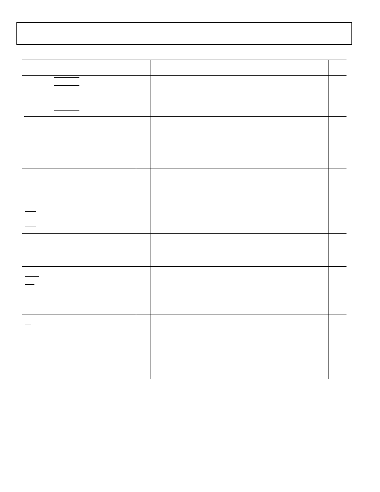
Figure 1. Processor Block Diagram
One Technology Way, P.O. Box 9106, Norwood, MA 02062-9106 U.S.A.
Tel: 781.329.4700 www.analog.com
Fax: 781.461.3113 © 2011 Analog Devices, Inc. All rights reserved.
Page 2

ADSP-BF592
TABLE OF CONTENTS
Features ................................................................. 1
Memory ................................................................ 1
Peripherals ............................................................. 1
General Description ................................................. 3
Portable Low Power Architecture ............................. 3
System Integration ................................................ 3
Blackfin Processor Core .......................................... 3
Memory Architecture ............................................ 5
Event Handling .................................................... 5
DMA Controllers .................................................. 6
Processor Peripherals ............................................. 6
Dynamic Power Management .................................. 8
Voltage Regulation ................................................ 9
Clock Signals ....................................................... 9
Booting Modes ................................................... 11
Instruction Set Description ................................... 12
Development Tools ............................................. 12
Designing an Emulator-Compatible
Processor Board (Target) ................................... 12
Related Documents .............................................. 12
Related Signal Chains ........................................... 12
Signal Descriptions ................................................. 13
Specifications ........................................................ 15
Operating Conditions ........................................... 15
Electrical Characteristics ....................................... 17
Absolute Maximum Ratings ................................... 19
ESD Sensitivity ................................................... 19
Package Information ............................................ 20
Timing Specifications ........................................... 21
Output Drive Currents ......................................... 35
Test Conditions .................................................. 36
Environmental Conditions .................................... 39
64-Lead LFCSP Lead Assignment ............................... 40
Outline Dimensions ................................................ 42
Automotive Products .............................................. 42
Ordering Guide ..................................................... 42
REVISION HISTORY
Rev. 0 to Rev. A
Added 200 MHz model to Electrical Characteristics ....... 17
Added 200 MHz model to Ordering Guide ................... 43
Rev. A | Page 2 of 44 | August 2011
Page 3

GENERAL DESCRIPTION
ADSP-BF592
The ADSP-BF592 processor is a member of the Blackfin® family
of products, incorporating the Analog Devices/Intel Micro
Signal Architecture (MSA). Blackfin processors combine a dualMAC state-of-the-art signal processing engine, the advantages
of a clean, orthogonal RISC-like microprocessor instruction set,
and single-instruction, multiple-data (SIMD) multimedia capabilities into a single instruction-set architecture.
The ADSP-BF592 processor is completely code compatible with
other Blackfin processors. The ADSP-BF592 processor offers
performance up to 400 MHz and reduced static power consumption. The processor features are shown in Table 1.
Table 1. Processor Features
Feature ADSP-BF592
Timer/Counters with PWM 3
SPORTs 2
SPIs 2
UART 1
Parallel Peripheral Interface 1
TWI 1
GPIOs 32
L1 Instruction SRAM 32K
L1 Instruction ROM 64K
L1 Data SRAM 32K
L1 Scratchpad SRAM 4K
Memory (bytes)
L3 Boot ROM 4K
Maximum Instruction Rate
Maximum System Clock Speed 100 MHz
Package Options 64-Lead LFCSP
1
Maximum instruction rate is not available with every possible SCLK selection.
1
400 MHz
By integrating a rich set of industry-leading system peripherals
and memory, Blackfin processors are the platform of choice for
next-generation applications that require RISC-like programmability, multimedia support, and leading-edge signal
processing in one integrated package.
PORTABLE LOW POWER ARCHITECTURE
Blackfin processors provide world-class power management
and performance. They are produced with a low power and low
voltage design methodology and feature on-chip dynamic
power management, which provides the ability to vary both the
voltage and frequency of operation to significantly lower overall
power consumption. This capability can result in a substantial
reduction in power consumption, compared with just varying
the frequency of operation. This allows longer battery life for
portable appliances.
head looping. The architecture is fully interlocked, meaning that
the programmer need not manage the pipeline when executing
SYSTEM INTEGRATION
The ADSP-BF592 processor is a highly integrated system-on-achip solution for the next generation of digital communication
and consumer multimedia applications. By combining industry
standard interfaces with a high performance signal processing
core, cost-effective applications can be developed quickly, without the need for costly external components. The system
peripherals include a watchdog timer; three 32-bit timers/counters with PWM support; two dual-channel, full-duplex
synchronous serial ports (SPORTs); two serial peripheral interface (SPI) compatible ports; one UART
®
with IrDA support; a
parallel peripheral interface (PPI); and a 2-wire interface (TWI)
controller.
BLACKFIN PROCESSOR CORE
As shown in Figure 2, the Blackfin processor core contains two
16-bit multipliers, two 40-bit accumulators, two 40-bit ALUs,
four video ALUs, and a 40-bit shifter. The computation units
process 8-, 16-, or 32-bit data from the register file.
The compute register file contains eight 32-bit registers. When
performing compute operations on 16-bit operand data, the
register file operates as 16 independent 16-bit registers. All
operands for compute operations come from the multiported
register file and instruction constant fields.
Each MAC can perform a 16-bit by 16-bit multiply in each
cycle, accumulating the results into the 40-bit accumulators.
Signed and unsigned formats, rounding, and saturation
are supported.
The ALUs perform a traditional set of arithmetic and logical
operations on 16-bit or 32-bit data. In addition, many special
instructions are included to accelerate various signal processing
tasks. These include bit operations such as field extract and population count, modulo 2
and rounding, and sign/exponent detection. The set of video
instructions includes byte alignment and packing operations,
16-bit and 8-bit adds with clipping, 8-bit average operations,
and 8-bit subtract/absolute value/accumulate (SAA) operations.
The compare/select and vector search instructions are also
provided.
For certain instructions, two 16-bit ALU operations can be performed simultaneously on register pairs (a 16-bit high half and
16-bit low half of a compute register). If the second ALU is used,
quad 16-bit operations are possible.
The 40-bit shifter can perform shifts and rotates and is used to
support normalization, field extract, and field deposit
instructions.
The program sequencer controls the flow of instruction execution, including instruction alignment and decoding. For
program flow control, the sequencer supports PC relative and
indirect conditional jumps (with static branch prediction) and
subroutine calls. Hardware is provided to support zero over
instructions with data dependencies.
32
multiply, divide primitives, saturation
Rev. A | Page 3 of 44 | August 2011
Page 4
ADSP-BF592
SEQUENCER
ALIGN
DECODE
LOOP BUFFER
16
16
8888
40 40
A0 A1
BARREL
SHIFTER
DATA ARITHMETIC UNIT
CONTROL
UNIT
R7.H
R6.H
R5.H
R4.H
R3.H
R2.H
R1.H
R0.H
R7.L
R6.L
R5.L
R4.L
R3.L
R2.L
R1.L
R0.L
AS TAT
40 40
32
32
32
32
32
32
32LD0
LD1
SD
DAG0
DAG1
ADDRESS ARITHMETIC UNIT
I3
I2
I1
I0
L3
L2
L1
L0
B3
B2
B1
B0
M3
M2
M1
M0
SP
FP
P5
P4
P3
P2
P1
P0
DA1
DA0
32
32
32
PREG
RAB
32
TO MEMORY
The address arithmetic unit provides two addresses for simultaneous dual fetches from memory. It contains a multiported
register file consisting of four sets of 32-bit index, modify,
length, and base registers (for circular buffering) and eight
additional 32-bit pointer registers (for C-style indexed stack
manipulation).
Blackfin processors support a modified Harvard architecture in
combination with a hierarchical memory structure. Level 1 (L1)
memories are those that typically operate at the full processor
speed with little or no latency. At the L1 level, the instruction
memory holds instructions only. Data memory holds data, and
a dedicated scratchpad data memory stores stack and local variable information.
Multiple L1 memory blocks are provided. The memory
management unit (MMU) provides memory protection for
individual tasks that may be operating on the core and can
protect system registers from unintended access.
The architecture provides three modes of operation: user mode,
supervisor mode, and emulation mode. User mode has
restricted access to certain system resources, thus providing a
protected software environment, while supervisor mode has
unrestricted access to the system and core resources.
The Blackfin processor instruction set has been optimized so
that 16-bit opcodes represent the most frequently used instructions, resulting in excellent compiled code density. Complex
DSP instructions are encoded into 32-bit opcodes, representing
fully featured multifunction instructions. Blackfin processors
support a limited multi-issue capability, where a 32-bit instruction can be issued in parallel with two 16-bit instructions,
allowing the programmer to use many of the core resources in a
single instruction cycle.
The Blackfin processor assembly language uses an algebraic syntax for ease of coding and readability. The architecture has been
optimized for use in conjunction with the C/C++ compiler,
resulting in fast and efficient software implementations.
Figure 2. Blackfin Processor Core
Rev. A | Page 4 of 44 | August 2011
Page 5
ADSP-BF592
0x0000 0000
0xEF00 0000
0xFF80 0000
0xFF80 8000
0xFFA0 0000
0xFFA0 8000
0xFFA1 0000
0xFFA2 0000
0xFFB0 0000
0xFFB0 1000
0xFFC0 0000
0xFFE0 0000
BOOT ROM (4K BYTES)
RESERVED
L1 INSTRUCTION ROM (64K BYTES)
RESERVED
L1 SCRATCHPAD RAM (4K BYTES)
RESERVED
SYSTEM MEMORY MAPPED REGISTERS (2M BYTES)
CORE MEMORY MAPPED REGISTERS (2M BYTES)
RESERVED
DATA SRAM (32K BYTES)
RESERVED
L1 INSTRUCTION BANK B SRAM (16K BYTES)
RESERVED
0xEF00 1000
0xFFFF FFFF
L1 INSTRUCTION BANK A SRAM (16K BYTES)
0xFFA0 4000
MEMORY ARCHITECTURE
The Blackfin processor views memory as a single unified
4G byte address space, using 32-bit addresses. All resources,
including internal memory and I/O control registers, occupy
separate sections of this common address space. See Figure 3.
The core-accessible L1 memory system is high performance
internal memory that operates at the core clock frequency. The
external bus interface unit (EBIU) provides access to the boot
ROM.
The memory DMA controller provides high bandwidth datamovement capability. It can perform block transfers of code or
data between the L1 Instruction SRAM and L1 Data SRAM
memory spaces.
Custom ROM (Optional)
The on-chip L1 Instruction ROM on the ADSP-BF592 may be
customized to contain user code with the following features:
• 64K bytes of L1 Instruction ROM available for custom code
• Ability to restrict access to all or specific segments of the
on-chip ROM
Customers wishing to customize the on-chip ROM for their
own application needs should contact ADI sales for more information on terms and conditions and details on the technical
implementation.
I/O Memory Space
The processor does not define a separate I/O space. All
resources are mapped through the flat 32-bit address space.
On-chip I/O devices have their control registers mapped into
memory-mapped registers (MMRs) at addresses near the top of
the 4G byte address space. These are separated into two smaller
blocks, one which contains the control MMRs for all core functions, and the other which contains the registers needed for
setup and control of the on-chip peripherals outside of the core.
The MMRs are accessible only in supervisor mode and appear
as reserved space to on-chip peripherals.
Booting from ROM
The processor contains a small on-chip boot kernel, which configures the appropriate peripheral for booting. If the processor is
configured to boot from boot ROM memory space, the processor starts executing from the on-chip boot ROM. For more
information, see Booting Modes on Page 11.
Figure 3. Internal/External Memory Map
Internal (Core-Accessible) Memory
The processor has three blocks of core-accessible memory, providing high bandwidth access to the core.
The first block is the L1 instruction memory, consisting of
32K bytes SRAM. This memory is accessed at full processor
speed.
The second core-accessible memory block is the L1 data memory, consisting of 32K bytes. This memory block is accessed at
full processor speed.
The third memory block is a 4K byte L1 scratchpad SRAM,
which runs at the same speed as the other L1 memories.
L1 Utility ROM
The L1 instruction ROM contains utility ROM code. This
includes the TMK (VDK core), C run-time libraries, and DSP
libraries. See the VisualDSP++ documentation for more
information.
Rev. A | Page 5 of 44 | August 2011
EVENT HANDLING
The event controller on the processor handles all asynchronous
and synchronous events to the processor. The processor
provides event handling that supports both nesting and prioritization. Nesting allows multiple event service routines to be
active simultaneously. Prioritization ensures that servicing of a
higher-priority event takes precedence over servicing of a lowerpriority event. The controller provides support for five different
types of events:
• Emulation – An emulation event causes the processor to
enter emulation mode, allowing command and control of
the processor via the JTAG interface.
• RESET
• Nonmaskable Interrupt (NMI) – The NMI event can be
– This event resets the processor.
generated by the software watchdog timer or by the NMI
input signal to the processor. The NMI event is frequently
used as a power-down indicator to initiate an orderly shutdown of the system.
Page 6

ADSP-BF592
• Exceptions – Events that occur synchronously to program
flow (in other words, the exception is taken before the
instruction is allowed to complete). Conditions such as
data alignment violations and undefined instructions cause
exceptions.
• Interrupts – Events that occur asynchronously to program
flow. They are caused by input signals, timers, and other
peripherals, as well as by an explicit software instruction.
Each event type has an associated register to hold the return
address and an associated return-from-event instruction. When
an event is triggered, the state of the processor is saved on the
supervisor stack.
The processor event controller consists of two stages: the core
event controller (CEC) and the system interrupt controller
(SIC). The core event controller works with the system interrupt
controller to prioritize and control all system events. Conceptually, interrupts from the peripherals enter into the SIC and are
then routed directly into the general-purpose interrupts of the
CEC.
Core Event Controller (CEC)
The CEC supports nine general-purpose interrupts (IVG15–7),
in addition to the dedicated interrupt and exception events. Of
these general-purpose interrupts, the two lowest priority
interrupts (IVG15–14) are recommended to be reserved for
software interrupt handlers, leaving seven prioritized interrupt
inputs to support the peripherals of the processor. The inputs to
the CEC, their names in the event vector table (EVT), and their
priorities are described in the ADSP-BF59x Blackfin Processor
Hardware Reference, “System Interrupts” chapter.
System Interrupt Controller (SIC)
The system interrupt controller provides the mapping and routing of events from the many peripheral interrupt sources to the
prioritized general-purpose interrupt inputs of the CEC.
Although the processor provides a default mapping, the user
can alter the mappings and priorities of interrupt events by writing the appropriate values into the interrupt assignment
registers (SIC_IARx). The inputs into the SIC and the default
mappings into the CEC are described in the ADSP-BF59x Black-
fin Processor Hardware Reference, “System Interrupts” chapter.
The SIC allows further control of event processing by providing
three pairs of 32-bit interrupt control and status registers. Each
register contains a bit, corresponding to each peripheral interrupt event. For more information, see the ADSP-BF59x Blackfin
Processor Hardware Reference, “System Interrupts” chapter.
DMA CONTROLLERS
The processor has multiple, independent DMA channels that
support automated data transfers with minimal overhead for
the processor core. DMA transfers can occur between the processor’s internal memories and any of its DMA-capable
peripherals. DMA-capable peripherals include the SPORTs, SPI
ports, UART, and PPI. Each individual DMA-capable peripheral has at least one dedicated DMA channel.
The processor DMA controller supports both one-dimensional
(1-D) and two-dimensional (2-D) DMA transfers. DMA transfer initialization can be implemented from registers or from sets
of parameters called descriptor blocks.
The 2-D DMA capability supports arbitrary row and column
sizes up to 64K elements by 64K elements, and arbitrary row
and column step sizes up to ±32K elements. Furthermore, the
column step size can be less than the row step size, allowing
implementation of interleaved data streams. This feature is
especially useful in video applications where data can be deinterleaved on the fly.
Examples of DMA types supported by the processor DMA controller include:
• A single, linear buffer that stops upon completion
• A circular, auto-refreshing buffer that interrupts on each
full or fractionally full buffer
• 1-D or 2-D DMA using a linked list of descriptors
• 2-D DMA using an array of descriptors, specifying only the
base DMA address within a common page
In addition to the dedicated peripheral DMA channels, there are
two memory DMA channels, which are provided for transfers
between the various memories of the processor system with
minimal processor intervention. Memory DMA transfers can be
controlled by a very flexible descriptor-based methodology or
by a standard register-based autobuffer mechanism.
PROCESSOR PERIPHERALS
The ADSP-BF592 processor contains a rich set of peripherals
connected to the core via several high bandwidth buses, providing flexibility in system configuration, as well as excellent
overall system performance (see Figure 1). The processor also
contains dedicated communication modules and high speed
serial and parallel ports, an interrupt controller for flexible management of interrupts from the on-chip peripherals or external
sources, and power management control functions to tailor the
performance and power characteristics of the processor and system to many application scenarios.
The SPORTs, SPIs, UART, and PPI peripherals are supported
by a flexible DMA structure. There are also separate memory
DMA channels dedicated to data transfers between the processor’s various memory spaces, including boot ROM. Multiple
on-chip buses running at up to 100 MHz provide enough bandwidth to keep the processor core running along with activity on
all of the on-chip and external peripherals.
The ADSP-BF592 processor includes an interface to an off-chip
voltage regulator in support of the processor’s dynamic power
management capability.
Watchdog Timer
The processor includes a 32-bit timer that can be used to implement a software watchdog function. A software watchdog can
improve system availability by forcing the processor to a known
state through generation of a hardware reset, nonmaskable
interrupt (NMI), or general-purpose interrupt, if the timer
expires before being reset by software. The programmer
Rev. A | Page 6 of 44 | August 2011
Page 7

ADSP-BF592
initializes the count value of the timer, enables the appropriate
interrupt, then enables the timer. Thereafter, the software must
reload the counter before it counts to zero from the programmed value. This protects the system from remaining in an
unknown state where software, which would normally reset the
timer, has stopped running due to an external noise condition
or software error.
If configured to generate a hardware reset, the watchdog timer
resets both the core and the processor peripherals. After a reset,
software can determine whether the watchdog was the source of
the hardware reset by interrogating a status bit in the watchdog
timer control register.
The timer is clocked by the system clock (SCLK) at a maximum
frequency of f
SCLK
.
Timers
There are four general-purpose programmable timer units in
the processor. Three timers have an external pin that can be
configured either as a pulse width modulator (PWM) or timer
output, as an input to clock the timer, or as a mechanism for
measuring pulse widths and periods of external events. These
timers can be synchronized to an external clock input to the several other associated PF pins, to an external clock input to the
PPI_CLK input pin, or to the internal SCLK.
The timer units can be used in conjunction with the UART to
measure the width of the pulses in the data stream to provide a
software auto-baud detect function for the respective serial
channels.
The timers can generate interrupts to the processor core providing periodic events for synchronization, either to the system
clock or to a count of external signals.
In addition to the three general-purpose programmable timers,
a fourth timer is also provided. This extra timer is clocked by the
internal processor clock and is typically used as a system tick
clock for generation of operating system periodic interrupts.
Serial Ports
The ADSP-BF592 processor incorporates two dual-channel
synchronous serial ports (SPORT0 and SPORT1) for serial and
multiprocessor communications. The SPORTs support the following features:
Serial port data can be automatically transferred to and from
on-chip memory/external memory via dedicated DMA channels. Each of the serial ports can work in conjunction with
another serial port to provide TDM support. In this configuration, one SPORT provides two transmit signals while the other
SPORT provides the two receive signals. The frame sync and
clock are shared.
Serial ports operate in five modes:
• Standard DSP serial mode
• Multichannel (TDM) mode
2
S mode
•I
2
•Packed I
S mode
•Left-justified mode
Serial Peripheral Interface (SPI) Ports
The processor has two SPI-compatible ports that enable the
processor to communicate with multiple SPI-compatible
devices.
The SPI interface uses three pins for transferring data: two data
pins (Master Output-Slave Input, MOSI, and Master InputSlave Output, MISO) and a clock pin (serial clock, SCK). An SPI
chip select input pin (SPIx_SS
) lets other SPI devices select the
processor, and many SPI chip select output pins (SPIx_SEL7–1
let the processor select other SPI devices. The SPI select pins are
reconfigured general-purpose I/O pins. Using these pins, the
SPI port provides a full-duplex, synchronous serial interface,
which supports both master/slave modes and multimaster
environments.
UART Port
The ADSP-BF592 processor provides a full-duplex universal
asynchronous receiver/transmitter (UART) port, which is fully
compatible with PC-standard UARTs. The UART port provides
a simplified UART interface to other peripherals or hosts,
supporting full-duplex, DMA-supported, asynchronous transfers of serial data. The UART port includes support for five to
eight data bits, one or two stop bits, and none, even, or odd parity. The UART port supports two modes of operation:
• PIO (programmed I/O) – The processor sends or receives
data by writing or reading I/O mapped UART registers.
The data is double-buffered on both transmit and receive.
• DMA (direct memory access) – The DMA controller transfers both transmit and receive data. This reduces the
number and frequency of interrupts required to transfer
data to and from memory. The UART has two dedicated
DMA channels, one for transmit and one for receive. These
DMA channels have lower default priority than most DMA
channels because of their relatively low service rates.
Parallel Peripheral Interface (PPI)
The processor provides a parallel peripheral interface (PPI) that
can connect directly to parallel analog-to-digital and digital-toanalog converters, video encoders and decoders, and other general-purpose peripherals. The PPI consists of a dedicated input
clock pin, up to three frame synchronization pins, and up to 16
data pins. The input clock supports parallel data rates up to half
the system clock rate, and the synchronization signals can be
configured as either inputs or outputs.
The PPI supports a variety of general-purpose and ITU-R 656
modes of operation. In general-purpose mode, the PPI provides
half-duplex, bidirectional data transfer with up to 16 bits of
data. Up to three frame synchronization signals are also provided. In ITU-R 656 mode, the PPI provides half-duplex
bidirectional transfer of 8- or 10-bit video data. Additionally,
on-chip decode of embedded start-of-line (SOL) and start-offield (SOF) preamble packets is supported.
)
Rev. A | Page 7 of 44 | August 2011
Page 8

ADSP-BF592
General-Purpose Mode Descriptions
The general-purpose modes of the PPI are intended to suit a
wide variety of data capture and transmission applications.
Three distinct submodes are supported:
• Input mode – Frame syncs and data are inputs into the PPI.
Input mode is intended for ADC applications, as well as
video communication with hardware signaling.
• Frame capture mode – Frame syncs are outputs from the
PPI, but data are inputs. This mode allows the video
source(s) to act as a slave (for frame capture for example).
• Output mode – Frame syncs and data are outputs from the
PPI. Output mode is used for transmitting video or other
data with up to three output frame syncs.
ITU-R 656 Mode Descriptions
The ITU-R 656 modes of the PPI are intended to suit a wide
variety of video capture, processing, and transmission applications. Three distinct submodes are supported:
• Active video only mode – Active video only mode is used
when only the active video portion of a field is of interest
and not any of the blanking intervals.
• Vertical blanking only mode – In this mode, the PPI only
transfers vertical blanking interval (VBI) data.
• Entire field mode – In this mode, the entire incoming bit
stream is read in through the PPI.
TWI Controller Interface
The processor includes a 2-wire interface (TWI) module for
providing a simple exchange method of control data between
multiple devices. The TWI is functionally compatible with the
widely used I
capabilities of simultaneous master and slave operation and
support for both 7-bit addressing and multimedia data arbitration. The TWI interface utilizes two pins for transferring clock
(SCL) and data (SDA) and supports the protocol at speeds up to
400K bits/sec.
The TWI module is compatible with serial camera control bus
(SCCB) functionality for easier control of various CMOS camera sensor devices.
2
C® bus standard. The TWI module offers the
Ports
The processor groups the many peripheral signals to two
ports—Port F and Port G. Most of the associated pins are shared
by multiple signals. The ports function as multiplexer controls.
General-Purpose I/O (GPIO)
The processor has 32 bidirectional, general-purpose I/O (GPIO)
pins allocated across two separate GPIO modules—PORTFIO
and PORTGIO, associated with Port F and Port G respectively.
Each GPIO-capable pin shares functionality with other processor peripherals via a multiplexing scheme; however, the GPIO
functionality is the default state of the device upon power-up.
Neither GPIO output nor input drivers are active by default.
Each general-purpose port pin can be individually controlled by
manipulation of the port control, status, and interrupt registers.
DYNAMIC POWER MANAGEMENT
The processor provides five operating modes, each with a different performance/power profile. In addition, dynamic power
management provides the control functions to dynamically alter
the processor core supply voltage, further reducing power dissipation. When configured for a 0 V core supply voltage, the
processor enters the hibernate state. Control of clocking to each
of the processor peripherals also reduces power consumption.
See Table 2 for a summary of the power settings for each mode.
Table 2. Power Settings
Core
PLL
Mode/State PLL
Full On Enabled No Enabled Enabled On
Active Enabled/
Disabled
Sleep Enabled — Disabled Enabled On
Deep Sleep Disabled — Disabled Disabled On
Hibernate Disabled — Disabled Disabled Off
Bypassed
Yes En ab le d En ab led O n
Clock
(CCLK)
Full-On Operating Mode—Maximum Performance
In the full-on mode, the PLL is enabled and is not bypassed,
providing capability for maximum operational frequency. This
is the power-up default execution state in which maximum performance can be achieved. The processor core and all enabled
peripherals run at full speed.
Active Operating Mode—Moderate Dynamic Power Savings
In the active mode, the PLL is enabled but bypassed. Because the
PLL is bypassed, the processor’s core clock (CCLK) and system
clock (SCLK) run at the input clock (CLKIN) frequency. DMA
access is available to appropriately configured L1 memories.
For more information about PLL controls, see the “Dynamic
Power Management” chapter in the ADSP-BF59x Blackfin Pro-
cessor Hardware Reference.
Sleep Operating Mode—High Dynamic Power Savings
The sleep mode reduces dynamic power dissipation by disabling
the clock to the processor core (CCLK). The PLL and system
clock (SCLK), however, continue to operate in this mode. Typically, an external event wakes up the processor.
System DMA access to L1 memory is not supported in
sleep mode.
Deep Sleep Operating Mode—Maximum Dynamic Power Savings
The deep sleep mode maximizes dynamic power savings by disabling the clocks to the processor core (CCLK) and to all
synchronous peripherals (SCLK). Asynchronous peripherals
may still be running but cannot access internal resources or
external memory. This powered-down mode can only be exited
by assertion of the reset interrupt (RESET
nous interrupt generated by a GPIO pin.
System
Clock
(SCLK)
) or by an asynchro-
Core
Power
Rev. A | Page 8 of 44 | August 2011
Page 9

Note that when a GPIO pin is used to trigger wake from deep
Power Savings Factor
f
CCLKRED
f
CCLKNOM
--------------------
V
DDINTRED
V
DDINTNOM
------------------------
2
×
T
RED
T
NOM
------------
×
=
% Power Savings 1 Power Savings Factor–()100%×=
sleep, the programmed wake level must linger for at least 10ns
to guarantee detection.
Hibernate State—Maximum Static Power Savings
The hibernate state maximizes static power savings by disabling
clocks to the processor core (CCLK) and to all of the peripherals
(SCLK), as well as signaling an external voltage regulator that
V
can be shut off. Any critical information stored inter-
DDINT
nally (for example, memory contents, register contents, and
other information) must be written to a nonvolatile storage
device prior to removing power if the processor state is to be
preserved. Writing b#0 to the HIBERNATE
bit causes
EXT_WAKE to transition low, which can be used to signal an
external voltage regulator to shut down.
Since V
can still be supplied in this mode, all of the exter-
DDEXT
nal pins three-state, unless otherwise specified. This allows
other devices that may be connected to the processor to still
have power applied without drawing unwanted current.
As long as V
is applied, the VR_CTL register maintains its
DDEXT
state during hibernation. All other internal registers and memories, however, lose their content in the hibernate state.
Power Savings
As shown in Table 3, the processor supports two different
power domains, which maximizes flexibility while maintaining
compliance with industry standards and conventions. By isolating the internal logic of the processor into its own power
domain, separate from other I/O, the processor can take advantage of dynamic power management without affecting the other
I/O devices. There are no sequencing requirements for the
various power domains, but all domains must be powered
according to the appropriate Specifications table for processor
operating conditions, even if the feature/peripheral is not used.
Table 3. Power Domains
Power Domain VDD Range
All internal logic and memories V
All other I/O V
DDINT
DDEXT
The dynamic power management feature of the processor
allows both the processor’s input voltage (V
quency (f
) to be dynamically controlled.
CCLK
) and clock fre-
DDINT
The power dissipated by a processor is largely a function of its
clock frequency and the square of the operating voltage. For
example, reducing the clock frequency by 25% results in a 25%
reduction in dynamic power dissipation, while reducing the
voltage by 25% reduces dynamic power dissipation by more
than 40%. Further, these power savings are additive, in that if
the clock frequency and supply voltage are both reduced, the
power savings can be dramatic, as shown in the following
equations.
ADSP-BF592
where:
f
f
V
V
T
T
VOLTAGE REGULATION
The ADSP-BF592 processor requires an external voltage regulator to power the V
consumption, the external voltage regulator can be signaled
through EXT_WAKE to remove power from the processor core.
This signal is high-true for power-up and may be connected
directly to the low-true shut-down input of many common
regulators.
While in the hibernate state, the external supply, V
still be applied, eliminating the need for external buffers. The
external voltage regulator can be activated from this powerdown state by asserting the RESET
boot sequence. EXT_WAKE indicates a wakeup to the external
voltage regulator.
The power good (PG
only after the internal voltage has reached a chosen level. In this
way, the startup time of the external regulator is detected after
hibernation. For a complete description of the power-good
functionality, refer to the ADSP-BF59x Blackfin Processor Hard-
ware Reference.
CLOCK SIGNALS
The processor can be clocked by an external crystal, a sine wave
input, or a buffered, shaped clock derived from an external
clock oscillator.
If an external clock is used, it should be a TTL-compatible signal
and must not be halted, changed, or operated below the specified frequency during normal operation. This signal is
connected to the processor’s CLKIN pin. When an external
clock is used, the XTAL pin must be left unconnected.
Alternatively, because the processor includes an on-chip oscillator circuit, an external crystal may be used. For fundamental
frequency operation, use the circuit shown in Figure 4. A
parallel -resonant, fundamental frequency, microprocessorgrade crystal is connected across the CLKIN and XTAL pins.
The on-chip resistance between CLKIN and the XTAL pin is in
is the nominal core clock frequency
CCLKNOM
is the reduced core clock frequency
CCLKRED
DDINTNOM
DDINTRED
NOM
RED
is the nominal internal supply voltage
is the reduced internal supply voltage
is the duration running at f
is the duration running at f
domain. To reduce standby power
DDINT
) input signal allows the processor to start
CCLKNOM
CCLKRED
, can
DDEXT
pin, which then initiates a
Rev. A | Page 9 of 44 | August 2011
Page 10
ADSP-BF592
CLKIN
CLKOUT (SCLK)
XTAL
SELECT
CLKBUF
TO PLL CIRCUITRY
FOR OVERTONE
OPERATION ONLY:
NOTE: VALUES MARKED WITH * MUST BE CUSTOMIZED, DEPENDING
ON THE CRYSTAL AND LAYOUT. PLEASE ANALYZE CAREFULLY. FOR
FREQUENCIES ABOVE 33 MHz, THE SUGGESTED CAPACITOR VALUE
OF 18 pF SHOULD BE TREATED AS A MAXIMUM, AND THE SUGGESTED
RESISTOR VALUE SHOULD BE REDUCED TO 0 ⍀.
18 pF *
EN
18 pF *
330 ⍀ *
BLACKFIN
560 ⍀
EXTCLK
EN
PLL
5u
to 64u
÷ 1 to 15
÷ 1, 2, 4, 8
VCO
CLKIN
“FINE” ADJUSTMENT
REQUIRES PLL SEQUENCING
“COARSE” ADJUSTMENT
ON-THE-FLY
CCLK
SCLK
SCLK d CCLK
the 500 kΩ range. Further parallel resistors are typically not recommended. The two capacitors and the series resistor shown in
Figure 4 fine tune phase and amplitude of the sine frequency.
The capacitor and resistor values shown in Figure 4 are typical
values only. The capacitor values are dependent upon the crystal
manufacturers’ load capacitance recommendations and the PCB
physical layout. The resistor value depends on the drive level
specified by the crystal manufacturer. The user should verify the
customized values based on careful investigations on multiple
devices over temperature range.
Figure 5. Frequency Modification Methods
All on-chip peripherals are clocked by the system clock (SCLK).
The system clock frequency is programmable by means of the
SSEL3–0 bits of the PLL_DIV register. The values programmed
into the SSEL fields define a divide ratio between the PLL output
(VCO) and the system clock. SCLK divider values are 1 through
15. Table 4 illustrates typical system clock ratios.
Note that the divisor ratio must be chosen to limit the system
clock frequency to its maximum of f
. The SSEL value can be
SCLK
changed dynamically without any PLL lock latencies by writing
the appropriate values to the PLL divisor register (PLL_DIV).
The core clock (CCLK) frequency can also be dynamically
changed by means of the CSEL1–0 bits of the PLL_DIV register.
Supported CCLK divider ratios are 1, 2, 4, and 8, as shown in
Table 5. This programmable core clock capability is useful for
fast core frequency modifications.
Figure 4. External Crystal Connections
A third-overtone crystal can be used for frequencies above
25 MHz. The circuit is then modified to ensure crystal operation
only at the third overtone, by adding a tuned inductor circuit as
shown in Figure 4. A design procedure for third-overtone operation is discussed in detail in (EE-168) Using Third Overtone
Crystals with the ADSP-218x DSP on the Analog Devices website (www.analog.com)—use site search on “EE-168.”
The Blackfin core runs at a different clock rate than the on-chip
peripherals. As shown in Figure 5, the core clock (CCLK) and
system peripheral clock (SCLK) are derived from the input
clock (CLKIN) signal. An on-chip PLL is capable of multiplying
the CLKIN signal by a programmable 5× to 64× multiplication
factor (bounded by specified minimum and maximum VCO
frequencies). The default multiplier is 6×, but it can be modified
by a software instruction sequence.
On-the-fly frequency changes can be effected by simply writing
to the PLL_DIV register. The maximum allowed CCLK and
SCLK rates depend on the applied voltages V
the VCO is always permitted to run up to the frequency specified by the part’s instruction rate. The EXTCLK pin can be
configured to output either the SCLK frequency or the input
buffered CLKIN frequency, called CLKBUF. When configured
to output SCLK (CLKOUT), the EXTCLK pin acts as a reference signal in many timing specifications. While three-stated by
default, it can be enabled using the VRCTL register.
DDINT
Table 5. Core Clock Ratios
Signal Name
CSEL1–0
00 1:1 300 300
01 2:1 300 150
10 4:1 400 100
11 8:1 200 25
Table 4. Example System Clock Ratios
Signal Name
SSEL3–0
0010 2:1 100 50
0110 6:1 300 50
1010 10:1 400 40
and V
DDEXT
;
The maximum CCLK frequency both depends on the part’s
instruction rate (see Page Page 43) and depends on the applied
V
voltage. See Table 8 for details. The maximal system
DDINT
clock rate (SCLK) depends on the chip package and the applied
and V
V
DDINT
Rev. A | Page 10 of 44 | August 2011
Divider Ratio
VCO/CCLK
Divider Ratio
VCO/SCLK
voltages (see Table 10).
DDEXT
Example Frequency Ratios
(MHz)
VCO CCLK
Example Frequency Ratios
(MHz)
VCO SCLK
Page 11

ADSP-BF592
BOOTING MODES
The processor has several mechanisms (listed in Table 6) for
automatically loading internal and external memory after a
reset. The boot mode is defined by the BMODE input pins dedicated to this purpose. There are two categories of boot modes.
In master boot modes, the processor actively loads data from
parallel or serial memories. In slave boot modes, the processor
receives data from external host devices.
Table 6. Booting Modes
BMODE2–0 Description
000 Idle/No Boot
001 Reserved
010 SPI1 master boot from Flash, using SPI1_SSEL5
011 SPI1 slave boot from external master
100 SPI0 master boot from Flash, using SPI0_SSEL2
101 Boot from PPI port
110 Boot from UART host device
111 Execute from Internal L1 ROM
The boot modes listed in Table 6 provide a number of mechanisms for automatically loading the processor’s internal and
external memories after a reset. By default, all boot modes use
the slowest meaningful configuration settings. Default settings
can be altered via the initialization code feature at boot time.
The BMODE pins of the reset configuration register, sampled
during power-on resets and software-initiated resets, implement the modes shown in Table 6.
• IDLE State/No Boot (BMODE - 0x0) — In this mode, the
boot kernel transitions the processor into Idle state. The
processor can then be controlled through JTAG for recovery, debug, or other functions.
• SPI1 master boot from flash (BMODE = 0x2) — In this
mode, SPI1 is configured to operate in master mode and to
connect to 8-, 16-, 24-, or 32-bit addressable devices. The
processor uses the PG11/SPI1_SSEL5
EEPROM/flash device, submits a read command and successive address bytes (0×00) until a valid 8-, 16-, 24-, or 32bit addressable device is detected, and begins clocking data
into the processor. Pull-up resistors are required on the
SSEL and MISO pins. By default, a value of 0×85 is written
to the SPI_BAUD register.
• SPI1 slave boot from external master (BMODE = 0x3) — In
this mode, SPI1 is configured to operate in slave mode and
to receive the bytes of the .LDR file from a SPI host (master) agent. To hold off the host device from transmitting
while the boot ROM is busy, the Blackfin processor asserts
a GPIO pin, called host wait (HWAIT), to signal to the host
device not to send any more bytes until the pin is deasserted. The host must interrogate the HWAIT signal,
available on PG4, before transmitting every data unit to the
processor. A pull-up resistor is required on the SPI1_SS
input. A pull-down on the serial clock may improve signal
quality and booting robustness.
to select a single SPI
on PG11
on PF8
• SPI0 master boot from flash (BMODE = 0x4) — In this
mode SPI0 is configured to operate in master mode and to
connect to 8-, 16-, 24-, or 32-bit addressable devices. The
processor uses the PF8/SPI0_SSEL2
EEPROM/flash device, submits a read command and successive address bytes (0×00) until a valid 8-, 16-, 24-, or 32bit addressable device is detected, and begins clocking data
into the processor. Pull-up resistors are required on the
SSEL and MISO pins. By default, a value of 0×85 is written
to the SPI_BAUD register.
• Boot from PPI host device (BMODE = 0x5) — The processor operates in PPI slave mode and is configured to receive
the bytes of the LDR file from a PPI host (master) agent.
• Boot from UART host device (BMODE = 0x6) — In this
mode UART0 is used as the booting source. Using an autobaud handshake sequence, a boot-stream formatted
program is downloaded by the host. The host selects a bit
rate within the UART clocking capabilities. When performing the autobaud, the UART expects a “@” (0×40)
character (eight bits data, one start bit, one stop bit, no parity bit) on the RXD pin to determine the bit rate. The
UART then replies with an acknowledgment which is composed of 4 bytes (0xBF—the value of UART_DLL) and
(0×00—the value of UART_DLH). The host can then
download the boot stream. To hold off the host the processor signals the host with the boot host wait (HWAIT)
signal. Therefore, the host must monitor the HWAIT, (on
PG4), before every transmitted byte.
• Execute from internal L1 ROM (BMODE = 0x7) — In this
mode the processor begins execution from the on-chip 64k
byte L1 instruction ROM starting at address 0xFFA1 0000.
For each of the boot modes (except Execute from internal L1
ROM), a 16 byte header is first brought in from an external
device. The header specifies the number of bytes to be transferred and the memory destination address. Multiple memory
blocks may be loaded by any boot sequence. Once all blocks are
loaded, program execution commences from the start of L1
instruction SRAM.
The boot kernel differentiates between a regular hardware reset
and a wakeup-from-hibernate event to speed up booting in the
latter case. Bits 7–4 in the system reset configuration (SYSCR)
register can be used to bypass the boot kernel or simulate a
wakeup-from-hibernate boot in case of a software reset.
The boot process can be further customized by “initialization
code.” This is a piece of code that is loaded and executed prior to
the regular application boot. Typically, this is used to speed up
booting by managing the PLL, clock frequencies, or serial bit
rates.
The boot ROM also features C-callable functions that can be
called by the user application at run time. This enables second
stage boot or boot management schemes to be implemented
with ease.
to select a single SPI
Rev. A | Page 11 of 44 | August 2011
Page 12

ADSP-BF592
INSTRUCTION SET DESCRIPTION
The Blackfin processor family assembly language instruction set
employs an algebraic syntax designed for ease of coding and
readability. The instructions have been specifically tuned to provide a flexible, densely encoded instruction set that compiles to
a very small final memory size. The instruction set also provides
fully featured multifunction instructions that allow the programmer to use many of the processor core resources in a single
instruction. Coupled with many features more often seen on
microcontrollers, this instruction set is very efficient when compiling C and C++ source code. In addition, the architecture
supports both user (algorithm/application code) and supervisor
(O/S kernel, device drivers, debuggers, ISRs) modes of operation, allowing multiple levels of access to core
processor resources.
The assembly language, which takes advantage of the processor’s unique architecture, offers the following advantages:
• Seamlessly integrated DSP/MCU features are optimized for
both 8-bit and 16-bit operations.
• A multi-issue load/store modified-Harvard architecture,
which supports two 16-bit MAC or four 8-bit ALU + two
load/store + two pointer updates per cycle.
• All registers, I/O, and memory are mapped into a unified
4G byte memory space, providing a simplified programming model.
• Microcontroller features, such as arbitrary bit and bit-field
manipulation, insertion, and extraction; integer operations
on 8-, 16-, and 32-bit data-types; and separate user and
supervisor stack pointers.
• Code density enhancements, which include intermixing of
16-bit and 32-bit instructions (no mode switching, no code
segregation). Frequently used instructions are encoded
in 16 bits.
DEVELOPMENT TOOLS
The processor is supported with a complete set of
CROSSCORE® software and hardware development tools,
including Analog Devices emulators and VisualDSP++® development environment. The same emulator hardware that
supports other Blackfin processors also fully emulates the
ADSP-BF592 processor.
EZ-KIT Lite® Evaluation Board
For evaluation of the ADSP-BF592 processor, use the EZ-KIT
Lite boards soon to be available from Analog Devices. When
these evaluation kits are available, order using part number
ADZS-BF592-EZLITE. The boards come with on-chip emulation capabilities and are equipped to enable software
development. Multiple daughter cards will be available.
DESIGNING AN EMULATOR-COMPATIBLE PROCESSOR BOARD (TARGET)
The Analog Devices family of emulators are tools that every system developer needs in order to test and debug hardware and
software systems. Analog Devices has supplied an IEEE 1149.1
JTAG Test Access Port (TAP) on each JTAG processor. The
emulator uses the TAP to access the internal features of the processor, allowing the developer to load code, set breakpoints,
observe variables, observe memory, and examine registers. The
processor must be halted to send data and commands, but once
an operation has been completed by the emulator, the processor
system is set running at full speed with no impact on
system timing.
To use these emulators, the target board must include a header
that connects the processor’s JTAG port to the emulator.
For details on target board design issues including mechanical
layout, single processor connections, multiprocessor scan
chains, signal buffering, signal termination, and emulator pod
logic, see (EE-68) Analog Devices JTAG Emulation Technical
Reference on the Analog Devices website (www.analog.com)—
use site search on “EE-68.” This document is updated regularly
to keep pace with improvements to emulator support.
RELATED DOCUMENTS
The following publications that describe the ADSP-BF592 processor (and related processors) can be ordered from any Analog
Devices sales office or accessed electronically on our website:
• Getting Started With Blackfin Processors
• ADSP-BF59x Blackfin Processor Hardware Reference
• Blackfin Processor Programming Reference
• ADSP-BF592 Blackfin Processor Anomaly List
RELATED SIGNAL CHAINS
A signal chain is a series of signal conditioning electronic com-
ponents that receive input (data acquired from sampling either
real-time phenomena or from stored data) in tandem, with the
output of one portion of the chain supplying input to the next.
Signal chains are often used in signal processing applications to
gather and process data or to apply system controls based on
analysis of real-time phenomena. For more information about
this term and related topics, see the “signal chain” entry in the
Glossary of EE Terms on the Analog Devices website.
Analog Devices eases signal processing system development by
providing signal processing components that are designed to
work together well. A tool for viewing relationships between
specific applications and related components is available on the
www.analog.com website.
The Circuits from the Lab
provides:
• Graphical circuit block diagram presentation of signal
chains for a variety of circuit types and applications
• Drill down links for components in each chain to selection
guides and application information
• Reference designs applying best practice design techniques
TM
site (www.analog.com\circuits)
Rev. A | Page 12 of 44 | August 2011
Page 13

SIGNAL DESCRIPTIONS
ADSP-BF592
Signal definitions for the ADSP-BF592 processor are listed in
Table 7. In order to maintain maximum function and reduce
package size and pin count, some pins have dual, multiplexed
functions. In cases where pin function is reconfigurable, the
default state is shown in plain text, while the alternate function
is shown in italics.
All pins are three-stated during and immediately after reset,
All I/O pins have their input buffers disabled with the exception
of the pins that need pull-ups or pull-downs, as noted in
Table 7.
Adding a parallel termination to EXTCLK may prove useful in
further enhancing signal integrity. Be sure to verify overshoot/undershoot and signal integrity specifications on actual
hardware.
with the exception of EXTCLK, which toggles at the system
clock rate.
Table 7. Signal Descriptions
Driver
Signal Name Type Function
Port F: GPIO and Multiplexed Peripherals
PF0–GPIO/DR1SEC/PPI_D8/WAK EN1 I/O GPIO/SPORT1 Receive Data Secondary/PPI Data 8/Wake Ena ble 1 A
PF1–GPIO/DR1PRI/PPI_D9 I/O GPIO/SPORT1 Receive Data Primary/PPI Data 9 A
PF2–GPIO/RSCLK1/PPI_D10 I/O GPIO/SPORT1 Receive Serial Clock/PPI Data 10 A
PF3–GPIO/RFS1/PPI_D11 I/O GPIO/SPORT1 Receive Frame Sync/PPI Data 11 A
PF4–GPIO/DT1 SEC/PPI_D12 I/O GPIO/SPORT1 Transmit Data Secondary/PPI Data 12 A
PF5–GPIO/DT1 PRI/PPI_D13 I/O GPIO/SPORT1 Transmit Data Primary/PPI Data 13 A
PF6–GPIO/TSCLK1/PPI_D14 I/O GPIO/SPORT1 Transmit Serial Clock/PPI Data 14 A
PF7–GPIO/TFS1/PPI_D15 I/O GPIO/SPORT1 Transmit Frame Sync/PPI Data 15 A
PF8–GPIO/TMR2/SPI0_SSEL2
PF9–GPIO/TMR0/PPI_FS1/SPI0_SSEL3
PF10–GPIO/TMR1/PPI_FS2 I/O GPIO/Timer 1/PPI Frame Sync 2 A
PF11–GPIO/UA_TX/SPI0_SSEL4
PF12–GPIO/UA_RX/SPI0_SSEL7
PF13–GPIO/SPI0_MOSI/SPI1_SSEL3
PF14–GPIO/SPI0_MISO/SPI1_SSEL4
PF15–GPIO/SPI0_SCK/SPI1_SSEL5
Port G: GPIO and Multiplexed Peripherals
PG0–GPIO/DR0SEC/SPI0_SSEL1
PG1–GPIO/DR0PRI/SPI1_SSEL1/WAK EN3 I/O GPIO/SPORT0 Receive Data Primary/SPI1 Slave Select Enable 1/Wake Enable 3 A
PG2–GPIO/RSCLK0/SPI0_SSEL5
PG3–GPIO/RFS0/PPI_FS3 I/O GPIO/SPORT0 Receive Frame Sync/PPI Frame Sync 3 A
PG4–GPIO(HWAIT)/DT 0SEC/SPI0_SSEL6
PG5–GPIO/DT0PR I/SPI1_SSEL6
PG6–GPIO/TSCLK0 I/O GPIO/SPORT0 Transmit Serial Clock A
PG7–GPIO/TFS0/SPI1_SSEL7
PG8–GPIO/SPI1_SCK/PPI_D0 I/O GPIO/SPI1 Clock/PPI Data 0 A
PG9–GPIO/SPI1_MOSI/PPI_D1 I/O GPIO/SPI1 Master Out Slave In/PPI Data 1 A
PG10–GPIO/SPI1_MISO/PPI_D2 I/O GPIO/SPI1 Master In Slave Out/PPI Data 2
/WAK EN0 I/O GPIO/Timer 2/SPI0 Slave Select Enable 2/Wake Enable 0 A
I/O GPIO/Timer 0/PPI Frame Sync 1/SPI0 Slave Select Enable 3 A
I/O GPIO/UART Transmit/SPI0 Slave Select Enable 4 A
/TACI2–0 I/O GPIO/UART Receive/SPI0 Slave Select Enable 7/Timers 2–0 Alternate Input
Capture
I/O GPIO/SPI0 Master Out Slave In/SPI1 Slave Select Enable 3 A
I/O GPIO/SPI0 Master In Slave Out/SPI1 Slave Select Enable 4
(This pin should always be pulled high through a 4.7 k resistor,
if booting via the SPI port.)
I/O GPIO/SPI0 Clock/SPI1 Slave Select Enable 5 A
/SPI0_SS I/O GPIO/SPORT0 Receive Data Secondary/SPI0 Slave Select Enable 1/SPI0 Slave
Select Input
I/O GPIO/SPORT0 Receive Serial Clock/SPI0 Slave Select Enable 5 A
I/O GPIO (HWAIT output for Slave Boot Modes)/SPORT0 Transmit Data
Secondary/SPI0 Slave Select Enable 6
I/O GPIO/SPORT0 Transmit Data Primary/SPI1 Slave Select Enable 6 A
I/O GPIO/SPORT0 Transmit Frame Sync/SPI1 Slave Select Enable 7 A
(This pin should always be pulled high through a 4.7 k resistor if booting via
the SPI port.)
Typ e
A
A
A
A
A
Rev. A | Page 13 of 44 | August 2011
Page 14
ADSP-BF592
Table 7. Signal Descriptions (Continued)
Signal Name Type Function
PG11–GPIO/SPI1_SSEL5/PPI_D3 I/O GPIO/SPI1 Slave Select Enable 5/PPI Data 3 A
PG12–GPIO/SPI1_SSEL2
PG13–GPIO/SPI1_SSEL1
PG14–GPIO/SPI1_SSEL4
PG15–GPIO/SPI1_SSEL6
TWI
SCL I/O TWI Serial Clock (This signal is an open-drain output and requires a pull-up
SDA I/O TWI Serial Data (This signal is an open-drain output and requires a pull-up
JTAG Port
TCK I JTAG CLK
TDO O JTAG Serial Data Out A
TDI I JTAG Serial Data In
TMS I JTAG Mode Select
TRST
EMU
Clock
CLKIN I CLK/Crystal In
XTAL O Crystal Output
EXTCLK O External Clock Output pin/System Clock Output C
Mode Controls
RESET
NMI
BMODE2–0 I Boot Mode Strap 2–0
PPI_CLK I PPI Clock Input
External Regulator Control
PG
EXT_WAKE O Wake up Indication A
Power Supplies ALL SUPPLIES MUST BE POWERED
V
DDEXT
V
DDINT
GND G Ground for All Supplies (Back Side of LFCSP Package.)
/PPI_D4/WAK EN2 I/O GPIO/SPI1 Slave Select Enable 2 Output/PPI Data 4/Wake E nabl e 2 A
/SPI1_SS/PPI_D5 I/O GPIO/SPI1 Slave Select Enable 1 Output/PPI Data 5/SPI1 Slave Select Input A
/PPI_D6/TACLK1 I/O GPIO/SPI1 Slave Select Enable 4/PPI Data 6/Timer 1 Auxiliary Clock Input A
/PPI_D7/TACLK2 I/O GPIO/SPI1 Slave Select Enable 6/PPI Data 7/Timer 2 Auxiliary Clock Input A
resistor. Consult version 2.1 of the I
2
C specification for the proper resistor
value.)
2
resistor. Consult version 2.1 of the I
C specification for the proper resistor
value.)
IJTAGReset
(This lead should be pulled low if the JTAG port is not used.)
O Emulation Output
I Reset
I Nonmaskable Interrupt
(Thisleadshouldbepulledhighwhennotused.)
I Power Good indication
See Operating Conditions on Page 15.
PI/OPowerSupply
P Internal Power Supply
Driver
Typ e
B
B
A
Rev. A | Page 14 of 44 | August 2011
Page 15

ADSP-BF592
SPECIFICATIONS
Specifications are subject to change without notice.
OPERATING CONDITIONS
Parameter Conditions Min Nominal Max Unit
V
V
V
V
V
V
V
V
V
V
V
V
T
T
T
1
Bidirectional leads (PF15–0, PG15–0) and input leads (TCK, TDI, TMS, TRST, CLKIN, RESET, NMI, and BMODE2–0) of the ADSP-BF592 processor are 3.3 V tolerant
(always accept up to 3.6 V maximum VIH). Voltage compliance (on outputs, VOH) is limited by the V
2
Parameter value applies to all input and bidirectional leads, except SDA and SCL.
3
Parameter applies to SDA and SCL.
Internal Supply Voltage Non-Automotive Models 1.1 1.47 V
DDINT
Internal Supply Voltage Automotive Models 1.33 1.47 V
External Supply Voltage Non-Automotive Models 1.7 1.8/2.5/3.3 3.6 V
DDEXT
External Supply Voltage Automotive Models 2.7 3.6 V
1, 2
1, 2
1, 2
3
1, 2
1, 2
1, 2
1, 2
1, 2
3
V
= 1.9 V 1.1 V
DDEXT
V
= 1.9 V 1.2 V
DDEXT
V
= 2.75 V 1.7 V
DDEXT
V
= 3.6 V 2.0 V
DDEXT
V
= 3.6 V 2.2 V
DDEXT
V
= 1.90 V/2.75 V/3.6 V 0.7 × V
DDEXT
V
= 1.7 V 0.6 V
DDEXT
V
= 2.25 V 0.7 V
DDEXT
V
= 3.0 V 0.8 V
DDEXT
V
= Minimum 0.3 × V
DDEXT
= 0°C to +70°C 0 80 °C
AMBIENT
= –40°C to +85°C –40 95 °C
AMBIENT
= –40°C to +105°C –40 115 °C
AMBIENT
DDEXT
DDEXT
supply voltage.
3.6 V
High Level Input Voltage
IH
High Level Input Voltage
IHCLKIN
High Level Input Voltage
IH
High Level Input Voltage
IH
High Level Input Voltage
IHCLKIN
High Level Input Voltage
IHTWI
Low Level Input Voltage
IL
Low Level Input Voltage
IL
Low Level Input Voltage
IL
Low Level Input Voltage
ILTWI
Junction Temperature 64-Lead LFCSP @ T
J
Junction Temperature 64-Lead LFCSP @ T
J
Junction Temperature 64-Lead LFCSP @ T
J
DDEXT
V
Rev. A | Page 15 of 44 | August 2011
Page 16

ADSP-BF592
ADSP-BF592 Clock Related Operating Conditions
Table 8 describes the core clock timing requirements for the
ADSP-BF592 processor. Take care in selecting MSEL, SSEL, and
CSEL ratios so as not to exceed the maximum core clock and
system clock (see Table 10). Table 9 describes phase-locked loop
operating conditions.
Table 8. Core Clock (CCLK) Requirements
Parameter
f
CCLK
Min V
DDINT
Nom V
DDINT
Core Clock Frequency (All Models) 1.33 V 1.400 V 400 MHz
Max CCLK
Frequency Unit
Core Clock Frequency (Industrial/Commercial Models) 1.16 V 1.225 V 300 MHz
Core Clock Frequency (Industrial/Commercial Models) 1.10 V 1.150 V 250
1
See the Ordering Guide on Page 43.
1
MHz
Table 9. Phase-Locked Loop Operating Conditions
Parameter Min Max Unit
f
VCO
Voltage Controlled Oscillator (VCO) Frequency
72 Instruction Rate
1
MHz
(Non-Automotive Models)
Voltage Controlled Oscillator (VCO) Frequency
84 Instruction Rate
1
MHz
(Automotive Models)
1
See the Ordering Guide on Page 43.
Table 10. Maximum SCLK Conditions
Parameter
f
SCLK
1
f
SCLK
1
CLKOUT/SCLK Frequency (V
CLKOUT/SCLK Frequency (V
must be less than or equal to f
CCLK
V
1.8 V/2.5 V/3.3 V Nominal Unit
DDEXT
≥1.16 V ) 100 MHz
DDINT
<1.16 V ) 80 MHz
DDINT
.
Rev. A | Page 16 of 44 | August 2011
Page 17

ADSP-BF592
ELECTRICAL CHARACTERISTICS
Parameter Test Conditions Min Typical Max Unit
V
OH
V
OH
V
OH
V
OL
V
Low Level Output Voltage V
OLTWI
I
IH
I
IL
I
IHP
I
OZH
I
OZHTWI
I
OZL
C
IN
I
DDDEEPSLEEP
I
DDSLEEP
I
DD-IDLE
I
DD-TYP
I
DD-TYP
I
DD-TYP
I
DDHIBERNATE
I
DDDEEPSLEEP
8
I
DDINT
1
Applies to input pins.
2
Applies to JTAG input pins (TCK, TDI, TMS, TRST).
3
Applies to three-statable pins.
4
Applies to bidirectional pins SCL and SDA.
5
Applies to all signal pins.
6
Guaranteed, but not tested.
7
See the ADSP-BF59x Blackfin Processor Hardware Reference Manual for definitions of sleep, deep sleep, and hibernate operating modes.
8
See Table 11 for the list of I
High Level Output Voltage V
High Level Output Voltage V
High Level Output Voltage V
Low Level Output Voltage V
High Level Input Current
Low Level Input Current
1
1
High Level Input Current JTAG
Three-State Leakage Current
Three-State Leakage Current
Three-State Leakage Current
Input Capacitance
7
V
Current in Deep Sleep Mode V
DDINT
V
Current in Sleep Mode V
DDINT
V
Current in Idle V
DDINT
V
Current V
DDINT
V
Current V
DDINT
V
Current V
DDINT
7
Hibernate State Current V
7
V
Current in Deep Sleep Mode f
DDINT
V
Current f
DDINT
DDINT
5
power vectors covered.
= 1.7 V, IOH = –0.5 mA 1.35 V
DDEXT
= 2.25 V, IOH = –0.5 mA 2.0 V
DDEXT
= 3.0 V, IOH = –0.5 mA 2.4 V
DDEXT
= 1.7 V/2.25 V/3.0 V,
DDEXT
= 2.0 mA
I
OL
= 1.7 V/2.25 V/3.0 V,
DDEXT
IOL=2.0mA
V
=3.6 V, VIN = 3.6 V 10 µA
DDEXT
V
=3.6 V, VIN = 0 V 10 µA
2
3
4
3
DDEXT
V
= 3.6 V, VIN = 3.6 V 10 50 µA
DDEXT
V
= 3.6 V, VIN = 3.6 V 10 µA
DDEXT
V
=3.0 V, VIN = 3.6 V 10 µA
DDEXT
V
= 3.6 V, VIN = 0 V 10 µA
DDEXT
fIN = 1 MHz, T
= 1.2 V, f
DDINT
=0MHz, T
f
SCLK
= 1.2 V, f
DDINT
= 25°C
T
J
= 1.2 V, f
DDINT
T
= 25°C, ASF = 0.35
J
= 1.3 V, f
DDINT
T
= 25°C, ASF = 1.00
J
= 1.3 V, f
DDINT
T
= 25°C, ASF = 1.00
J
= 1.4 V, f
DDINT
= 25°C, ASF = 1.00
T
J
=3.3V, TJ= 25°C,
DDEXT
= 25°C, VIN = 2.5 V 4 8
AMBIENT
= 0 MHz,
CCLK
= 25°C, ASF = 0.00
J
= 25 MHz,
SCLK
= 50 MHz,
CCLK
= 200 MHz,
CCLK
= 300 MHz,
CCLK
= 400 MHz,
CCLK
0.8 mA
4mA
6mA
40 mA
66 mA
91 mA
20 A
0.4 V
0.4 V
6
V
pF
CLKIN = 0 MHz with voltage
regulator off (V
= 0 MHz, f
CCLK
> 0 MHz, f
CCLK
= 0 V)
DDINT
= 0 MHz Tab le 1 2 mA
SCLK
≥ 0 MHz Ta bl e 1 2 +
SCLK
mA
(Tab le 13 × ASF)
Rev. A | Page 17 of 44 | August 2011
Page 18

ADSP-BF592
Total Power Dissipation
Total power dissipation has two components:
1. Static, including leakage current
2. Dynamic, due to transistor switching characteristics
Many operating conditions can also affect power dissipation,
including temperature, voltage, operating frequency, and processor activity. Electrical Characteristics on Page 17 shows the
current dissipation for internal circuitry (V
DDINT
). I
DDDEEPSLEEP
specifies static power dissipation as a function of voltage
) and temperature (see Table 12), and I
(V
DDINT
specifies the
DDINT
total power specification for the listed test conditions, including
the dynamic component as a function of voltage (V
DDINT
frequency (Table 13).
There are two parts to the dynamic component. The first part is
due to transistor switching in the core clock (CCLK) domain.
This part is subject to an Activity Scaling Factor (ASF), which
represents application code running on the processor core and
L1 memories (Table 11).
) and
The ASF is combined with the CCLK frequency and V
DDINT
dependent data in Table 13 to calculate this part. The second
part is due to transistor switching in the system clock (SCLK)
domain, which is included in the I
Table 11. Activity Scaling Factors (ASF)
I
Power Vector Activity Scaling Factor (ASF)
DDINT
I
DD-PEAK
I
DD-HIGH
I
DD-TYP
I
DD-APP
I
DD-NOP
I
DD-IDLE
1
See Estimating Power for ASDP-BF534/BF536/BF537 Blackfin Processors
(EE-297). The power vector information also applies to the ADSP-BF592
processor.
specification equation.
DDINT
1
1.29
1.26
1.00
0.83
0.66
0.33
Table 12. Static Current - I
1
TJ (°C)
1.15 V 1.20 V 1.25 V 1.30 V 1.35 V 1.40 V 1.45 V 1.50 V
DD-DEEPSLEEP
(mA)
Voltage (V
DDINT
1
)
25 0.85 0.98 1.13 1.29 1.46 1.62 1.85 2.07
40 1.57 1.8 2.012.162.512.743.053.36
55 2.57 2.88 3.2 3.5 3.84 4.22 4.63 5.05
70 4.04 4.45 4.86 5.3 5.81 6.31 6.87 7.45
85 6.52 7.12 7.73 8.36 9.09 9.86 10.67 11.54
100 9.67 10.51 11.37 12.24 13.21 14.26 15.37 16.55
115 14.18 15.29 16.45 17.71 19.05 20.45 21.96 23.56
1
Valid temperature and voltage ranges are model-specific. See Operating Conditions on Page 15.
Table 13. Dynamic Current in CCLK Domain (mA, with ASF = 1.0)
f
CCLK
2
(MHz)
1.15 V 1.20 V 1.25 V 1.30 V 1.35 V 1.40 V 1.45 V 1.50 V
1
Voltage (V
DDINT
2
)
400 N/A N/A N/A N/A 85.31 88.96 92.81 96.63
350 N/A N/A N/A 72.08 75.41 78.70 82.07 85.46
300 N/A 57.52 60.38 63.22 66.14 69.02 71.93 75.05
250 46.10 48.43 50.76 53.19 55.68 58.17 60.69 63.23
200 37.86 39.80 41.76 43.79 45.81 47.85 49.97 52.09
100 21.45 22.56 23.78 24.98 25.97 26.64 27.92 29.98
1
The values are not guaranteed as stand-alone maximum specifications. They must be combined with static current per the equations of Electrical Characteristics on Page 17.
2
Valid frequency and voltage ranges are model-specific. See Operating Conditions on Page 15 and Table 8 on Page 16.
Rev. A | Page 18 of 44 | August 2011
Page 19

ADSP-BF592
ABSOLUTE MAXIMUM RATINGS
Stresses greater than those listed in Table 14 may cause permanent damage to the device. These are stress ratings only.
Functional operation of the device at these or any other conditions greater than those indicated in the operational sections of
this specification is not implied. Exposure to absolute maximum
rating conditions for extended periods may affect device
reliability.
Table 14. Absolute Maximum Ratings
Parameter Rating
Internal Supply Voltage (V
External (I/O) Supply Voltage (V
Input Voltage
1, 2
Output Voltage Swing –0.5 V to V
I
Current per Pin Group 55 mA (Max)
OH/IOL
I
Current per Individual Pin 25 mA (Max)
OH/IOL
Storage Temperature Range – 65°C to +150°C
Junction Temperature While Biased
(Non-Automotive Models)
Junction Temperature While Biased
(Automotive Models)
1
Applies to 100% transient duty cycle. For other duty cycles see Table 15.
2
Applies only when V
fications, the range is V
is within specifications. When V
DDEXT
DDEXT
Table 15. Maximum Duty Cycle for Input Transient Voltage
VIN Min (V)
2
VIN Max (V)
–0.5 +3.8 100%
–0.7 +4.0 40%
–0.8 +4.1 25%
–0.9 +4.2 15%
–1.0 +4.3 10%
1
Applies to all signal pins with the exception of CLKIN, XTAL, EXT_WAKE.
2
The individual values cannot be combined for analysis of a single instance of
overshoot or undershoot. The worst case observed value must fall within one of
the voltages specified, and the total duration of the overshoot or undershoot
(exceeding the 100% case) must be less than or equal to the corresponding duty
cycle.
3
Duty cycle refers to the percentage of time the signal exceeds the value for the
100% case. The is equivalent to the measured duration of a single instance of
overshoot or undershoot as a percentage of the period of occurrence.
) 1.16 V to +1.47 V
DDINT
)–0.3 V to +3.8 V
DDEXT
–0.5 V to +3.6 V
+110°C
+115°C
± 0.2 Volts.
2
Maximum Duty Cycle
+0.5 V
DDEXT
is outside speci-
DDEXT
3
Table 16. Note that the V
and VOL specifications have separate
OH
per-pin maximum current requirements, see the Electrical
Characteristics table.
Table 16. Total Current Pin Groups–V
DDEXT
Groups
Group Pins in Group
1 PF0, PF1, PF2, PF3
2 PF4, PF5, PF6, PF7
3 PF8, PF9, PF10, PF11
4 PF12, PF13, PF14, PF15
5 PG3, PG2, PG1, PG0
6 PG7, PG6, PG5, PG4
7 PG11, PG10, PG9, PG8
8 PG15, PG14, PG13, PG12
9 TDI, TDO, EMU, TCK, TRST
, TMS
10 BMODE2, BMODE1, BMODE0
11 EXT_WAKE, PG, RESET, NMI, PPI_CLK, EXTCLK
12 SDA, SCL, CLKIN, XTAL
ESD SENSITIVITY
ESD (electrostatic discharge) sensitive device.
Charged devices and circuit boards can discharge
without detection. Although this product features
patented or proprietary circuitry, damage may occur
1
on devices subjected to high energy ESD. Therefore,
proper ESD precautions should be taken to avoid
performance degradation or loss of functionality.
Table 14 specifies the maximum total source/sink (I
OH/IOL
) current for a group of pins and for individual pins. Permanent
damage can occur if this value is exceeded. To understand this
specification, if pins PF0 and PF1 from Group 1 in Table 16
were sourcing or sinking 10 mA each, the total current for those
pins would be 20 mA. This would allow up to 35 mA total that
could be sourced or sunk by the remaining pins in the group
without damaging the device. It should also be noted that the
maximum source or sink current for an individual pin cannot
exceed 25 mA. The list of all groups and their pins are shown in
Rev. A | Page 19 of 44 | August 2011
Page 20

ADSP-BF592
vvvvvv .x n. n
tppZccc
ADSP-BF592
a
#yyww country_of_origin
B
PACKAGE INFORMATION
The information presented in Figure 6 and Table 17 provides
details about the package branding for the ADSP-BF592 processor. For a complete listing of product availability, see Ordering
Guide on Page 43.
Figure 6. Product Information on Package
Table 17. Package Brand Information
Brand Key Field Description
ADSP-BF592 Product Name
t Temperature Range
pp Package Type
Z RoHS Compliant Designation
ccc See Ordering Guide
vvvvvv.x Assembly Lot Code
n.n Silicon Revision
# RoHS Compliance Designator
yyww Date Code
Rev. A | Page 20 of 44 | August 2011
Page 21

ADSP-BF592
CLKIN
t
WRST
t
CKIN
t
CKINL
t
CKINH
t
BUFDLAY
t
BUFDLAY
RESET
CLKBUF
TIMING SPECIFICATIONS
Specifications are subject to change without notice.
Clock and Reset Timing
Table 18 and Figure 7 describe clock and reset operations. Per
the CCLK and SCLK timing specifications in Table 8 to
Table 10, combinations of CLKIN and clock multipliers must
not select core/peripheral clocks in excess of the processor’s
instruction rate.
Table 18. Clock and Reset Timing
V
1.8 V Nominal V
DDEXT
Parameter Min Max Min Max Unit
Timing Requirements
f
CKIN
t
CKINL
t
CKINH
t
WRST
CLKIN Period
CLKIN Low Pulse
CLKIN High Pulse
RESET Asserted Pulse Width Low
1, 2, 3, 4
1
1
5
10 10 ns
10 10 ns
11 × t
CKIN
11 × t
12 50 12 50 MHz
Switching Characteristic
t
BUFDLAY
1
Applies to PLL bypass mode and PLL non bypass mode.
2
Combinations of the CLKIN frequency and the PLL clock multiplier must not exceed the allowed f
on Page 16.
3
The t
4
If the DF bit in the PLL_CTL register is set, the minimum f
5
Applies after power-up sequence is complete. See Table 19 and Figure 8 for power-up reset timing.
6
The ADSP-BF592 processor does not have a dedicated CLKBUF pin. Rather, the EXTCLK pin may be programmed to serve as CLKBUF or CLKOUT. This parameter applies
when EXTCLK is programmed to output CLKBUF.
CLKIN to CLKBUF6 Delay 11 10 ns
, f
, and f
settings discussed in Table 8 on Page 16 through Table 10
SCLK
period (see Figure 7) equals 1/f
CKIN
CKIN
VCO
CCLK
.
specification is 24 MHz.
CKIN
2.5 V/3.3 V Nominal
DDEXT
CKIN
ns
Figure 7. Clock and Reset Timing
Rev. A | Page 21 of 44 | August 2011
Page 22

ADSP-BF592
RESET
t
RST_IN_PWR
CLKIN
V
DD_SUPPLIES
Table 19. Power-Up Reset Timing
Parameter Min Max Unit
Timing Requirements
t
RST_IN_PWR
RESET Deasserted after the V
Specification
DDINT
, V
, and CLKIN Pins are Stable and within
DDEXT
Figure 8. Power-Up Reset Timing
3500 × t
CKIN
s
Rev. A | Page 22 of 44 | August 2011
Page 23

Parallel Peripheral Interface Timing
PPI_CLK
PPI_FS1/2
t
PSUD
t
PCLK
t
SFSPE
DATA SAMPLED /
FRAME SYNC SAMPLED
DATA SAMPLED /
FRAME SYNC SAMPLED
PPI_DATA
PPI_CLK
PPI_FS1/2
t
HFSPE
t
HDRPE
t
SDRPE
t
PCLKW
Table 20 and Figure 9 through Figure 13 describe parallel
peripheral interface operations.
Table 20. Parallel Peripheral Interface Timing
ADSP-BF592
Parameter
= 1.8 V V
V
DDEXT
Min Max Min Max Unit
= 2.5 V/3.3 V
DDEXT
Timing Requirements
t
PCLKW
t
PCLK
PPI_CLK Width
PPI_CLK Period
1
1
t
–1.5 t
SCLK
2 × t
–1.5 2 × t
SCLK
–1.5 ns
SCLK
–1.5 ns
SCLK
Timing Requirements—GP Input and Frame Capture Modes
t
PSUD
t
SFSPE
External Frame Sync Startup Delay
External Frame Sync Setup Before PPI_CLK
2
4 × t
PCLK
4 × t
PCLK
ns
6.7 6.7 ns
(Nonsampling Edge for Rx, Sampling Edge for Tx)
t
HFSPE
t
SDRPE
t
HDRPE
External Frame Sync Hold After PPI_CLK 1.8 1.6 ns
Receive Data Setup Before PPI_CLK 4.1 3.5 ns
Receive Data Hold After PPI_CLK 2 1.6 ns
Switching Characteristics—GP Output and Frame Capture Modes
t
DFSPE
t
HOFSPE
t
DDTPE
t
HDTPE
1
PPI_CLK frequency cannot exceed f
2
The PPI port is fully enabled 4 PPI clock cycles after the PAB write to the PPI port enable bit. Only after the PPI port is fully enabled are external frame syncs and data words
guaranteed to be received correctly by the PPI peripheral.
Internal Frame Sync Delay After PPI_CLK 9.0 8.0 ns
Internal Frame Sync Hold After PPI_CLK 1.7 1.7 ns
Transmit Data Delay After PPI_CLK 8.7 8.0 ns
Transmit Data Hold After PPI_CLK 2.3 1.9 ns
/2
SCLK
Figure 9. PPI with External Frame Sync Timing
Figure 10. PPI GP Rx Mode with External Frame Sync Timing
Rev. A | Page 23 of 44 | August 2011
Page 24

ADSP-BF592
t
HDTPE
t
SFSPE
DATA DRIVEN /
FRAME SYNC SAMPLED
PPI_DATA
PPI_CLK
PPI_FS1/2
t
HFSPE
t
DDTPE
t
PCLK
t
PCLKW
t
HDRPE
t
SDRPE
t
HOFSPE
FRAME SYNC
DRIVEN
DATA
SAMPLED
PPI_DATA
PPI_CLK
PPI_FS1/2
t
DFSPE
t
PCLK
t
PCLKW
t
HOFSPE
FRAME SYNC
DRIVEN
DATA
DRIVEN
PPI_DATA
PPI_CLK
PPI_FS1/2
t
DFSPE
t
DDTPE
t
HDTPE
t
PCLK
t
PCLKW
DATA
DRIVEN
Figure 11. PPI GP Tx Mode with External Frame Sync Timing
Figure 12. PPI GP Rx Mode with Internal Frame Sync Timing
Figure 13. PPI GP Tx Mode with Internal Frame Sync Timing
Rev. A | Page 24 of 44 | August 2011
Page 25

Serial Ports
Table 21 through Table 25 and Figure 14 through Figure 18
describe serial port operations.
Table 21. Serial Ports—External Clock
ADSP-BF592
Parameter
Timing Requirements
t
SFSE
t
HFSE
t
SDRE
t
HDRE
t
SCLKEW
t
SCLKE
t
SUDTE
t
SUDRE
TFSx/RFSx Setup Before TSCLKx/RSCLKx
TFSx/RFSx Hold After TSCLKx/RSCLKx
Receive Data Setup Before RSCLKx
Receive Data Hold After RSCLKx
TSCLKx/RSCLKx Width 4.5 4.5 ns
TSCLKx/RSCLKx Period 2 × t
Start-Up Delay From SPORT Enable To First External TFSx24 × t
Start-Up Delay From SPORT Enable To First External RFSx24 × t
Switching Characteristics
t
DFSE
TFSx/RFSx Delay After TSCLKx/RSCLKx
(Internally Generated TFSx/RFSx)
t
HOFSE
TFSx/RFSx Hold After TSCLKx/RSCLKx
(Internally Generated TFSx/RFSx)
t
DDTE
t
HDTE
1
Referenced to sample edge.
2
Verified in design but untested.
3
Referenced to drive edge.
Transmit Data Delay After TSCLKx
Transmit Data Hold After TSCLKx
Table 22. Serial Ports—Internal Clock
V
DDEXT
1.8V Nominal
V
DDEXT
2.5 V/3.3V Nominal
Min Max Min Max Unit
1
1
1
1
3
1
1
1
33ns
33ns
33ns
3.5 3 ns
SCLK
TSCLKE
RSCLKE
2 × t
4 × t
4 × t
SCLK
TSCLKE
RSCLKE
ns
ns
ns
10 10 ns
00ns
11 10 ns
00ns
Parameter
Timing Requirements
t
t
t
t
SFSI
HFSI
SDRI
HDRI
TFSx/RFSx Setup Before TSCLKx/RSCLKx
TFSx/RFSx Hold After TSCLKx/RSCLKx
Receive Data Setup Before RSCLKx
Receive Data Hold After RSCLKx
Switching Characteristics
t
SCLKIW
t
DFSI
TSCLKx/RSCLKx Width 7 8 ns
TFSx/RFSx Delay After TSCLKx/RSCLKx
(Internally Generated TFSx/RFSx)
t
HOFSI
TFSx/RFSx Hold After TSCLKx/RSCLKx
(Internally Generated TFSx/RFSx)
t
DDTI
t
HDTI
1
Referenced to sample edge.
2
Referenced to drive edge.
Transmit Data Delay After TSCLKx
Transmit Data Hold After TSCLKx
V
DDEXT
1.8V Nominal
V
DDEXT
2.5 V/3.3V Nominal
Min Max Min Max Unit
1
1
1
1
2
1
1
1
11.5 9.6 ns
–1.5 –1.5 ns
11.5 11.3 ns
–1.5 –1.5 ns
43ns
–2 –2 ns
43ns
–1.8 –1.5 ns
Rev. A | Page 25 of 44 | August 2011
Page 26

ADSP-BF592
t
SDRI
RSCLKx
DRx
DRIVE EDGE
t
HDRI
t
SFSI
t
HFSI
t
DFSI
t
H
OFSI
t
SCLKIW
DATA RECEIVE—INTERNAL CLOCK
t
SDRE
DATA RECEIVE—EXTERNAL CLOCK
RSCLKx
DRx
t
HDRE
t
SFSE
t
HFSE
t
DFSE
t
SCLKEW
t
HOFSE
t
DDTI
t
HDTI
TSCLKx
TFSx
(INPUT)
DTx
t
SFSI
t
HFSI
t
SCLKIW
t
DFSI
t
HOFSI
DATA TRANSMIT—INTERNAL CLOCK
t
DDTE
t
HDTE
TSCLKx
DTx
t
SFSE
t
DFSE
t
SCLKE W
t
HOFSE
DATA TR ANSMIT—E XTERNAL CLOCK
SAMPLE EDGE
DRIVE EDGE SAMPLE EDGE DRIVE EDGE SAMPLE EDGE
DRIVE EDGE SAMPLE EDGE
t
SCLKE
t
SCLKE
t
HFSE
TFSx
(OUTPUT)
TFSx
(INPUT)
TFSx
(OUTPUT)
RFSx
(INPUT)
RFSx
(OUTPUT)
RFSx
(INPUT)
RFSx
(OUTPUT)
TSCLKx
(INPUT)
TFSx
(INPUT)
RFSx
(INPUT)
RSCLKx
(INPUT)
t
SUDTE
t
SUDRE
FIRST
TSCLKx/RSCLKx
EDGE AFTER
SPORT ENABLED
Figure 14. Serial Ports
Figure 15. Serial Port Start Up with External Clock and Frame Sync
Rev. A | Page 26 of 44 | August 2011
Page 27

Table 23. Serial Ports—Enable and Three-State
TSCLKx
DTx
DRIVE EDGE
t
DDTTE/I
t
DTENE/I
DRIVE EDGE
ADSP-BF592
Parameter
Switching Characteristics
t
DTENE
t
DDTTE
t
DTENI
t
DDTTI
1
Referenced to drive edge.
Data Enable Delay from External TSCLKx
Data Disable Delay from External TSCLKx
Data Enable Delay from Internal TSCLKx
Data Disable Delay from Internal TSCLKx
V
DDEXT
1.8V Nominal
Min Max Min Max Unit
1
1
1
1
Figure 16. Serial Ports — Enable and Three-State
00ns
–2 –2 ns
2.5 V/3.3V Nominal
t
+ 1 t
SCLK
t
+ 1 t
SCLK
V
DDEXT
+ 1 ns
SCLK
+ 1 ns
SCLK
Rev. A | Page 27 of 44 | August 2011
Page 28

ADSP-BF592
RSCLKx
RFSx
DTx
DRIVE
EDGE
DRIVE
EDGE
SAMPLE
EDGE
EXTERNAL RFSx IN MULTI-CHANNEL MODE
1ST BIT
t
DTENLFSE
t
DDTLFSE
TSCLKx
TFSx
DTx
DRIVE
EDGE
DRIVE
EDGE
SAMPLE
EDGE
LATE EXTERNAL TFSx
1ST BIT
t
DDTLFSE
Table 24. Serial Ports—External Late Frame Sync
Parameter
Switching Characteristics
t
DDTLFSE
Data Delay from Late External TFSx
or External RFSx in multi-channel mode with MFD = 0
t
DTENL FSE
1
When in multi-channel mode, TFSx enable and TFSx valid follow t
2
If external RFSx/TFSx setup to RSCLKx/TSCLKx > t
Data Enable from External RFSx in multi-channel mode with
MFD = 0
1, 2
SCLKE
/2 then t
DTENLFSE
DDTTE/I
and t
and t
1, 2
.
DDTLFSE
apply, otherwise t
DTENE/I
V
DDEXT
1.8V Nominal
V
DDEXT
2.5 V/3.3V Nominal
Min Max Min Max Unit
12 10 ns
00ns
DDTLFSE
and t
DTENLFSE
apply.
Figure 17. Serial Ports — External Late Frame Sync
Rev. A | Page 28 of 44 | August 2011
Page 29

Table 25. Serial Ports—Gated Clock Mode
TSCLKx
(OUT)
GATED CLOCK MODE DATA RECEIVE
TFS/TMR
(OUT)
DTx
DELAY TIME DATA TRANSMIT
t
HDRI
t
SDRI
TSCLKx
(OUT)
TSCLKx
(OUT)
t
DDTI
t
HDTI
DRx
t
DFTSCLKCNV
t
DCNVLTSCLK
t
DCNVLTSCLK
t
DFTSCLKCNV
ADSP-BF592
V
DDEXT
1.8V Nominal
V
DDEXT
2.5 V/3.3 V Nominal
Parameter Min Max Min Max Unit
Timing Requirements
t
t
SDRI
HDRI
Receive Data Setup Before TSCLKx 11.3 8.7 ns
Receive Hold After TSCLKx 0 0 ns
Switching Characteristics
t
DDTI
t
HDTI
t
DFTSCLKCNV
t
DCNVLTSCLK
Transmit Data Delay After TSCLKx 3 3 ns
Transmit Data Hold After TSCLKx –1.8 –1.8 ns
First TSCLKx edge delay after TFSx/TMR1 Low 0.5 × t
TFSx/TMR1 High Delay After Last TSCLKx Edge t
TSCLK
– 3 0.5 × t
TSCLK
– 3 t
– 3 ns
TSCLK
– 3 ns
TSCLK
Figure 18. Serial Ports Gated Clock Mode
Rev. A | Page 29 of 44 | August 2011
Page 30

ADSP-BF592
t
SDSCIM
t
SPICLK
t
HDSM
t
SPITDM
t
SPICLM
t
SPICHM
t
HDSPIDM
t
HSPIDM
t
SSPIDM
SPIxSELy
(OUTPUT)
SPIxSCK
(OUTPUT)
SPIxMOSI
(OUTPUT)
SPIxMISO
(INPUT)
SPIxMOSI
(OUTPUT)
SPIxMISO
(INPUT)
CPHA = 1
CPHA = 0
t
DDSPIDM
t
HSPIDM
t
SSPIDM
t
HDSPIDM
t
DDSPIDM
Serial Peripheral Interface (SPI) Port—Master Timing
Table 26 and Figure 19 describe SPI port master operations.
Table 26. Serial Peripheral Interface (SPI) Port—Master Timing
Parameter
Timing Requirements
t
SSPIDM
t
HSPIDM
Data Input Valid to SCK Edge (Data Input Setup) 11.6 9.6 ns
SCK Sampling Edge to Data Input Invalid –1.5 –1.5 ns
Switching Characteristics
t
SDSCIM
t
SPICHM
t
SPICLM
t
SPICLK
t
HDSM
t
SPITDM
t
DDSPIDM
t
HDSPIDM
SPI_SELx low to First SCK Edge 2 × t
Serial Clock High Period 2 × t
Serial Clock Low Period 2 × t
Serial Clock Period 4 × t
Last SCK Edge to SPI_SELx High 2 × t
Sequential Transfer Delay 2 × t
SCK Edge to Data Out Valid (Data Out Delay) 0606ns
SCK Edge to Data Out Invalid (Data Out Hold) –1 –1 ns
V
DDEXT
1.8V Nominal
V
DDEXT
2.5 V/3.3V Nominal
Min Max Min Max Unit
– 1.5 2 × t
SCLK
– 1.5 2 × t
SCLK
– 1.5 2 × t
SCLK
– 1.5 4 × t
SCLK
– 2 2 × t
SCLK
– 1.5 2 × t
SCLK
– 1.5 ns
SCLK
– 1.5 ns
SCLK
– 1.5 ns
SCLK
– 1.5 ns
SCLK
– 1.5 ns
SCLK
– 1.5 ns
SCLK
Figure 19. Serial Peripheral Interface (SPI) Port—Master Timing
Rev. A | Page 30 of 44 | August 2011
Page 31

Serial Peripheral Interface (SPI) Port—Slave Timing
t
SPICLK
t
HDS
t
SPITDS
t
SDSCI
t
SPICLS
t
SPICHS
t
DSOE
t
DDSPID
t
DDSPID
t
DSDHI
t
HDSPID
t
SSPID
t
DSDHI
t
HDSPID
t
DSOE
t
HSPID
t
SSPID
t
DDSPID
SPIxSS
(INPUT)
SPIxSCK
(INPUT)
SPIxMISO
(OUTPUT)
SPIxMOSI
(INPUT)
SPIxMISO
(OUTPUT)
SPIxMOSI
(INPUT)
CPHA = 1
CPHA = 0
t
HSPID
Table 27 and Figure 20 describe SPI port slave operations.
Table 27. Serial Peripheral Interface (SPI) Port—Slave Timing
ADSP-BF592
Parameter
Timing Requirements
t
SPICHS
t
SPICLS
t
SPICLK
t
HDS
t
SPITDS
t
SDSCI
t
SSPID
t
HSPID
Serial Clock High Period 2 × t
Serial Clock Low Period 2 × t
Serial Clock Period 4 × t
Last SCK Edge to SPI_SS Not Asserted 2 × t
Sequential Transfer Delay 2 × t
SPI_SS Assertion to First SCK Edge 2 × t
Data Input Valid to SCK Edge (Data Input Setup) 1.6 1.6 ns
SCK Sampling Edge to Data Input Invalid 2 1.6 ns
Switching Characteristics
t
DSOE
t
DSDHI
t
DDSPID
t
HDSPID
SPI_SS Assertion to Data Out Active 0 12 0 10.3 ns
SPI_SS Deassertion to Data High Impedance 0 11 0 9 ns
SCK Edge to Data Out Valid (Data Out Delay) 10 10 ns
SCK Edge to Data Out Invalid (Data Out Hold) 0 0 ns
V
DDEXT
1.8V Nominal
V
DDEXT
2.5 V/3.3V Nominal
Min Max Min Max Unit
– 1.5 2 × t
SCLK
– 1.5 2 × t
SCLK
4 × t
SCLK
– 1.5 2 × t
SCLK
– 1.5 2 × t
SCLK
– 1.5 2 × t
SCLK
– 1.5 ns
SCLK
– 1.5 ns
SCLK
ns
SCLK
– 1.5 ns
SCLK
– 1.5 ns
SCLK
– 1.5 ns
SCLK
Figure 20. Serial Peripheral Interface (SPI) Port—Slave Timing
Rev. A | Page 31 of 44 | August 2011
Page 32

ADSP-BF592
CLKOUT
GPIO OUTPUT
GPIO INPUT
t
WFI
t
GPOD
Universal Asynchronous Receiver-Transmitter (UART) Ports—Receive and Transmit Timing
The UART ports receive and transmit operations are described
in the ADSP-BF59x Hardware Reference Manual.
General-Purpose Port Timing
Table 28 and Figure 21 describe general-purpose
port operations.
Table 28. General-Purpose Port Timing
Parameter
Timing Requirement
t
WFI
Switching Characteristics
t
GPOD
General-Purpose Port Pin Input Pulse Width t
General-Purpose Port Pin Output Delay from CLKOUT Low 0 11 ns
1.8V/2.5 V/3.3 V Nominal
V
DDEXT
Min Max Unit
+ 1 ns
SCLK
Figure 21. General-Purpose Port Timing
Rev. A | Page 32 of 44 | August 2011
Page 33

Timer Cycle Timing
CLKOUT
TMRx OUTPUT
TMRx INPUT
t
TIS
t
TIH
tWH,t
WL
t
TOD
t
HTO
PPI_CLK
TMRx OUTPUT
t
TODP
Table 29 and Figure 22 describe timer expired operations. The
input signal is asynchronous in “width capture mode” and
“external clock mode” and has an absolute maximum input frequency of (f
SCLK
/2) MHz.
Table 29. Timer Cycle Timing
ADSP-BF592
V
DDEXT
2.5 V/3.3V Nominal
Parameter
V
DDEXT
1.8V Nominal
Min Max Min Max Unit
Timing Requirements
t
WL
t
WH
t
TIS
t
TIH
Timer Pulse Width Input Low
(Measured In SCLK Cycles)
Timer Pulse Width Input High
(Measured In SCLK Cycles)
1
1
Timer Input Setup Time Before CLKOUT Low
Timer Input Hold Time After CLKOUT Low
2
1 × t
SCLK
1 × t
SCLK
2
10 8 ns
1 × t
1 × t
SCLK
SCLK
–2 –2 ns
Switching Characteristics
t
HTO
Timer Pulse Width Output
1 × t
– 2 (232 – 1) × t
SCLK
SCLKtSCLK
– 1.5 (232 – 1) × t
SCLK
(Measured In SCLK Cycles)
t
TOD
1
The minimum pulse widths apply for TMRx signals in width capture and external clock modes. They also apply to the PG0 or PPI_CLK signals in PWM output mode.
2
Either a valid setup and hold time or a valid pulse width is sufficient. There is no need to resynchronize programmable flag inputs.
Timer Output Update Delay After CLKOUT High 6 6 ns
ns
ns
ns
Timer Clock Timing
Table 30 and Figure 23 describe timer clock timing.
Table 30. Timer Clock Timing
Parameter
Switching Characteristic
t
TODP
Timer Output Update Delay After PPI_CLK High 12.64 12.64 ns
Figure 22. Timer Cycle Timing
V
DDEXT
Min Max Min Max Unit
Figure 23. Timer Clock Timing
Rev. A | Page 33 of 44 | August 2011
= 1.8 V V
= 2.5V/3.3 V
DDEXT
Page 34

ADSP-BF592
TCK
TMS
TDI
TDO
SYSTEM
INPUTS
SYSTEM
OUTPUTS
t
TCK
t
STAP
t
HTAP
t
DTDO
t
SSYS
t
HSYS
t
DSYS
JTAG Test And Emulation Port Timing
Table 31 and Figure 24 describe JTAG port operations.
Table 31. JTAG Port Timing
Parameter
Timing Requirements
t
TCK
t
STAP
t
HTAP
t
SSYS
t
HSYS
t
TRSTW
TCK Period 20 20 ns
TDI, TMS Setup Before TCK High 4 4 ns
TDI, TMS Hold After TCK High 4 4 ns
System Inputs Setup Before TCK High
System Inputs Hold After TCK High
1
1
TRST Pulse Width2 (measured in TCK cycles) 4 4 TCK
Switching Characteristics
t
DTDO
t
DSYS
1
System inputs = SCL, SDA, PF15–0, PG15–0, PH2–0, TCK, NMI, BMODE3–0, PG.
2
50 MHz maximum
3
System outputs = CLKOUT, SCL, SDA, PF15–0, PG15–0, PH2–0, TDO, EMU, EXT_WAKE.
TDO Delay from TCK Low 10 10 ns
System Outputs Delay After TCK Low
3
V
DDEXT
1.8V Nominal
V
DDEXT
2.5 V/3.3V Nominal
Min Max Min Max Unit
45ns
55ns
13 13 ns
Figure 24. JTAG Port Timing
Rev. A | Page 34 of 44 | August 2011
Page 35

OUTPUT DRIVE CURRENTS
0
SOURCE CURRENT (mA)
120
100
40
–100
–40
V
OL
V
OH
80
–60
–80
–20
20
60
SOURCE VOLTAGE (V)
0 0.5 1.0 1.5 2.0 2.5 3.0 3.5
V
DDEXT
= 3.0V @ – 40°C
V
DDEXT
= 3.3V @ 25°C
V
DDEXT
= 3.6V @ 105°C
0
SOURCE CURRENT (mA)
SOURCE VOLTAGE (V)
0 0.5 1.0 1.5 2.0 2.5
80
60
20
–80
–60
–20
V
OL
V
OH
V
DDEXT
= 2.75V @ – 40°C
V
DDEXT
= 2.5V @ 25°C
40
–40
V
DDEXT
= 2.25V @ 105°C
0
SOURCE CURRENT (mA)
SOURCE VOLTAGE (V)
0 0.5 1.0 1.5
40
30
20
–40
–30
–10
V
OL
V
OH
–20
10
V
DDEXT
= 1.9V @ – 40°C
V
DDEXT
= 1.8V @ 25°C
V
DDEXT
= 1.7V @ 105°C
0 0.5 1.0 1.5 2.0 2.5 3.0 3.5
0
SOURCE CURRENT (mA)
SOURCE VOLTAGE (V)
120
100
40
–120
–100
–40
V
OL
V
DDEXT
= 3.6V @ – 40°C
V
DDEXT
= 3.3V @ 25°C
80
–60
V
DDEXT
= 3.0V @ 105°C
–80
–20
20
60
0
SOURCE CURRENT (mA)
SOURCE VOLTAGE (V)
0 0.5 1.0 1.5 2.0 2.5
80
60
20
–80
–60
–20
V
OL
V
DDEXT
= 2.75V @ – 40°C
V
DDEXT
= 2.5V @ 25°C
40
–40
V
DDEXT
= 2.25V @ 105°C
Figure 25 through Figure 33 show typical current-voltage char-
acteristics for the output drivers of the ADSP-BF592 processor.
The curves represent the current drive capability of the output
drivers. See Table 7 on Page 13 for information about which
driver type corresponds to a particular pin.
ADSP-BF592
Figure 25. Driver Type A Current (3.3V V
Figure 26. Drive Type A Current (2.5V V
DDEXT
DDEXT
Figure 27. Driver Type A Current (1.8V V
DDEXT
)
)
Figure 28. Driver Type B Current (3.3V V
DDEXT
)
)
Figure 29. Driver Type B Current (2.5V V
DDEXT
)
Rev. A | Page 35 of 44 | August 2011
Page 36

ADSP-BF592
0
SOURCE CURRENT (mA)
SOURCE VOLTAGE (V)
0 0.5 1.0 1.5
30
20
–30
–10
V
OL
V
DDEXT
= 1.9V @ – 40°C
V
DDEXT
= 1.8V @ 25°C
–20
–40
10
40
V
DDEXT
= 1.7V @ 105°C
50
–50
0
SOURCE CURRENT (mA)
SOURCE VOLTAGE (V)
0 0.5 1.0 1.5 2.0 2.5 3.0 3.5
90
60
– 90
– 30
V
OL
V
OH
V
DDEXT
= 3.6V @ – 40°C
V
DDEXT
= 3.3V @ 25°C
– 60
– 150
30
120
V
DDEXT
= 3.0V @ 105°C
– 120
150
0
SOURCE CURRENT (mA)
SOURCE VOLTAGE (V)
0 0.5 1.0 1.5 2.0 2.5
100
– 100
– 25
V
OL
V
OH
V
DDEXT
= 2.75V @ – 40°C
V
DDEXT
= 2.5V @ 25°C
– 50
V
DDEXT
= 2.25V @ 105°C
– 75
25
50
75
0
SOURCE CURRENT (mA)
SOURCE VOLTAGE (V)
0 0.5 1.0 1.5
60
40
–60
–20
V
OL
V
OH
V
DDEXT
= 1.9V @ – 40°C
V
DDEXT
= 1.8V @ 25°C
–40
20
V
DDEXT
= 1.7V @ 105°C
INPUT
OR
OUTPUT
V
MEAS
V
MEAS
REFERENCE
SIGNAL
t
DIS
OUTPUT STARTS DRIVING
V
OH
(MEASURED) ⴚ ⌬V
V
OL
(MEASURED) + ⌬V
t
DIS_MEASURED
V
OH
(MEASURED)
V
OL
(MEASURED)
V
TRIP
(HIGH)
V
OH
(MEASURED
)
VOL(MEASURED)
HIGH IMPEDANCE STATE
OUTPUT STOPS DRIVING
t
ENA
t
DECAY
t
ENA_M EASURED
t
TRIP
V
TRIP
(LOW)
Figure 30. Driver Type B Current (1.8V V
Figure 31. Driver Type C Current (3.3V V
DDEXT
DDEXT
)
Figure 33. Driver Type C Current (1.8V V
DDEXT
)
TEST CONDITIONS
All timing parameters appearing in this data sheet were measured under the conditions described in this section. Figure 34
shows the measurement point for ac measurements (except output enable/disable). The measurement point V
for V
(nominal) = 1.8 V/2.5 V/3.3 V.
DDEXT
Figure 34. Voltage Reference Levels for AC
Measurements (Except Output Enable/Disable)
Output Enable Time Measurement
)
Output pins are considered to be enabled when they have made
a transition from a high impedance state to the point when they
start driving.
The output enable time t
is the interval from the point when
ENA
a reference signal reaches a high or low voltage level to the point
when the output starts driving as shown on the right side of
Figure 35.
MEAS
is V
DDEXT
/2
Figure 32. Driver Type C Current (2.5V V
)
DDEXT
Rev. A | Page 36 of 44 | August 2011
Figure 35. Output Enable/Disable
Page 37

ADSP-BF592
t
ENAtENA_MEASUREDtTRIP
–=
t
DIStDIS_MEASUREDtDECAY
–=
t
DECAY
CLVΔ()I
L
⁄=
T1
ZO = 50:(impedance)
TD = 4.04 r 1.18 ns
2pF
TESTER PIN ELECTRONICS
50:
0.5pF
70:
400:
45:
4pF
NOTES:
THE WORST CASE TRANSMISSION LINE DELAY IS SHOWN AND CAN BE USED
FOR THE OUTPUT TIMING ANALYSIS TO REFELECT THE TRANSMISSION LINE
EFFECT AND MUST BE CONSIDERED. THE TRANSMISSION LINE (TD) IS FOR
LOAD ONLY AND DOES NOT AFFECT THE DATA SHEET TIMING SPECIFICATIONS.
ANALOG DEVICES RECOMMENDS USING THE IBIS MODEL TIMING FOR A GIVEN
SYSTEM REQUIREMENT. IF NECESSARY, A SYSTEM MAY INCORPORATE
EXTERNAL DRIVERS TO COMPENSATE FOR ANY TIMING DIFFERENCES.
V
LOAD
DUT
OUTPUT
50:
8
RISE AND FALL TIME (ns)
LOAD CAPACITANCE (pF)
0 50 100 150 250
18
14
0
2
6
12
200
t
RISE
t
FALL
t
FALL
= 1.8V @ 25°C
t
RISE
= 1.8V @ 25°C
4
10
16
20
The time t
ENA_MEASURED
signal switches to when the output voltage reaches V
or V
(low) and is shown below.
TRIP
•V
(nominal) = 1.8 V, V
DDEXT
is the interval from when the reference
(high)
TRIP
(high) is 1.05 V, V
TRIP
TRIP
(low) is 0.75 V
•V
(nominal) = 2.5 V, V
DDEXT
(high) is 1.5 V, V
TRIP
TRIP
(low)
is 1.0 V
•V
(nominal) = 3.3 V, V
DDEXT
(high) is 1.9 V, V
TRIP
TRIP
(low)
is 1.4 V
Time t
when the output reaches the V
is the interval from when the output starts driving to
TRIP
(high) or V
TRIP
(low) trip
TRIP
voltage.
Time t
is calculated as shown in the equation:
ENA
If multiple pins are enabled, the measurement value is that of
the first lead to start driving.
Output Disable Time Measurement
Output pins are considered to be disabled when they stop driving, go into a high impedance state, and start to decay from their
output high or low voltage. The output disable time t
difference between t
DIS_MEASURED
and t
as shown on the left
DECAY
DIS
is the
side of Figure 35.
Capacitive Loading
Output delays and holds are based on standard capacitive loads
of an average of 6 pF on all pins (see Figure 36). V
to (V
)/2.
DDEXT
Figure 36. Equivalent Device Loading for AC Measurements
(Includes All Fixtures)
LOAD
is equal
The time for the voltage on the bus to decay by ΔV is dependent
on the capacitive load C
and the load current IL. This decay
L
time can be approximated by the equation:
The time t
ΔV equal to 0.25 V for V
0.15 V for V
The time t
is calculated with test loads CL and IL, and with
DECAY
(nominal) = 1.8V.
DDEXT
DIS_MEASURED
is the interval from when the reference
(nominal) = 2.5 V/3.3 V and
DDEXT
signal switches to when the output voltage decays ΔV from the
measured output high or output low voltage.
Example System Hold Time Calculation
To determine the data output hold time in a particular system,
first calculate t
using the equation given above. Choose ΔV
DECAY
to be the difference between the processor’s output voltage and
the input threshold for the device requiring the hold time. C
the total bus capacitance (per data line), and I
L
age or three-state current (per data line). The hold time will be
t
plus the various output disable times as specified in the
DECAY
Timing Specifications on Page 21.
The graphs of Figure 37 through Figure 42 show how output
rise time varies with capacitance. The delay and hold specifications given should be derated by a factor derived from these
figures. The graphs in these figures may not be linear outside the
ranges shown.
is
L
is the total leak-
Rev. A | Page 37 of 44 | August 2011
Figure 37. Driver Type A Typical Rise and Fall Times (10%–90%) vs.
Load Capacitance (1.8V V
DDEXT
)
Page 38

ADSP-BF592
8
RISE AND FALL TIME (ns)
LOAD CAPACITANCE (pF)
0 50 100 150 250
18
14
0
2
6
12
200
t
RISE
t
FALL
t
FALL
= 2.5V @ 25°C
t
RISE
= 2.5V @ 25°C
4
10
16
8
RISE AND FALL TIME (ns)
LOAD CAPACITANCE (pF)
0 50 100 150 250
12
0
2
4
10
200
t
RISE
t
FALL
6
14
t
FALL
= 3.3V @ 25°C
t
RISE
= 3.3V @ 25°C
6
RISE AND FALL TIME (ns)
LOAD CAPACITANCE (pF)
0 50 100 150 250
12
10
0
2
4
8
200
t
RISE
t
FALL
t
FALL
= 1.8V @ 25°C
t
RISE
= 1.8V @ 25°C
4
RISE AND FALL TIME (ns)
LOAD CAPACITANCE (pF)
0 50 100 150 250
9
7
0
1
3
6
200
t
RISE
t
FALL
t
FALL
= 2.5V @ 25°C
t
RISE
= 2.5V @ 25°C
2
5
8
4
RISE AND FALL TIME (ns)
LOAD CAPACITANCE (pF)
0 50 100 150 250
7
6
0
1
2
5
200
t
RISE
t
FALL
3
t
FALL
= 3.3V @ 25°C
t
RISE
= 3.3V @ 25°C
Figure 38. Driver Type A Typical Rise and Fall Times (10%–90%) vs.
Load Capacitance (2.5V V
16
DDEXT
)
Figure 39. Driver Type A Typical Rise and Fall Times (10%–90%) vs.
Load Capacitance (3.3V V
DDEXT
)
Figure 41. Driver Type C Typical Rise and Fall Times (10%–90%) vs.
Load Capacitance (2.5V V
DDEXT
)
Figure 42. Driver Type C Typical Rise and Fall Times (10%–90%) vs.
Load Capacitance (3.3V V
DDEXT
)
Figure 40. Driver Type C Typical Rise and Fall Times (10%–90%) vs.
Load Capacitance (1.8V V
)
DDEXT
Rev. A | Page 38 of 44 | August 2011
Page 39

ENVIRONMENTAL CONDITIONS
TJT
CASE
ΨJTP
D
×()+=
TJTAθJAP
D
×()+=
To determine the junction temperature on the application
printed circuit board use:
where:
T
= junction temperature (°C)
J
= case temperature (°C) measured by customer at top cen-
T
CASE
ter of package.
Ψ
= from Table 32
JT
= power dissipation (see Total Power Dissipation on Page 18
P
D
for the method to calculate P
Table 32. Thermal Characteristics
Parameter Condition Typical Unit
q
JA
θ
JMA
θ
JMA
θ
JB
θ
JC
Ψ
JT
Ψ
JT
Ψ
JT
0 linear m/s air flow 23.5 °C/W
1 linear m/s air flow 20.9 °C/W
2 linear m/s air flow 20.2 °C/W
0 linear m/s air flow 0.21 °C/W
1 linear m/s air flow 0.36 °C/W
2 linear m/s air flow 0.43 °C/W
)
D
11.2 °C/W
9.5 °C/W
ADSP-BF592
Values of
circuit board design considerations.
order approximation of T
θ
are provided for package comparison and printed
JA
by the equation:
J
θ
can be used for a first
JA
where:
T
= ambient temperature (°C)
A
θ
Values of
are provided for package comparison and printed
JC
circuit board design considerations when an external heat sink
is required.
θ
Values of
are provided for package comparison and printed
JB
circuit board design considerations.
In Table 32, airflow measurements comply with JEDEC standards JESD51-2 and JESD51-6, and the junction-to-board
measurement complies with JESD51-8. The junction-to-case
measurement complies with MIL-STD-883 (Method 1012.1).
All measurements use a 2S2P JEDEC test board.
Rev. A | Page 39 of 44 | August 2011
Page 40

ADSP-BF592
64-LEAD LFCSP LEAD ASSIGNMENT
Table 33 lists the LFCSP leads by signal mnemonic. Table 34
lists the LFCSP by lead number.
Table 33. 64-Lead LFCSP Lead Assignment (Alphabetical by Signal)
Signal Lead No. Signal Lead No. Signal Lead No. Signal Lead No.
BMODE0 29 PF7 7 PG6 38 TDO 23
BMODE1 28 PF8 10 PG7 39 TMS 21
BMODE2 27 PF9 11 PG8 42 TRST
EXTCLK/SCLK57PF1012PG943V
CLKIN61PF1113PG1044V
EMU
19 PF12 15 PG11 45 V
EXT_WAKE 51 PF13 16 PG12 47 V
GND30PF1417PG1348V
NMI
PF0 63 PG
54 PF15 18 PG14 49 V
52 PG15 50 V
PF1 64 PG0 31 PPI_CLK 56 V
PF2 1 PG1 32 RESET
53 V
PF3 2 PG2 33 SCL 60 V
PF4 4 PG3 34 SDA 59 V
PF5 5 PG4 36 TCK 24 V
DDEXT
DDEXT
DDEXT
DDEXT
DDEXT
DDEXT
DDINT
DDINT
DDINT
DDINT
DDINT
DDINT
PF6 6 PG5 37 TDI 22 XTAL 62
*
GND
* Lead no. 65 is the GND supply (see Figure 43 and Figure 44) for the processor (6.2 mm × 6.2 mm); this pad must connect to GND.
20
3
14
25
35
46
58
8
9
26
40
41
55
65
Table 34. 64-Lead LFCSP Lead Assignment (Numerical by Lead Number)
Lead No. Signal Lead No. Signal Lead No. Signal Lead No. Signal
1 PF2 17 PF14 33 PG2 49 PG14
2 PF3 18 PF15 34 PG3 50 PG15
3V
DDEXT
4PF420TRST
19 EMU 35 V
36 PG4 52 PG
DDEXT
51 EXT_WAKE
5 PF5 21 TMS 37 PG5 53 RESET
6PF622TDI38PG654NMI
7PF723TDO39PG755V
8V
9V
DDINT
DDINT
10 PF8 26 V
24 TCK 40 V
25 V
DDEXT
DDINT
41 V
42 PG8 58 V
DDINT
DDINT
56 PPI_CLK
57 EXTCLK/SCLK
DDINT
DDEXT
11PF927BMODE243PG959SDA
12 PF10 28 BMODE1 44 PG10 60 SCL
13 PF11 29 BMODE0 45 PG11 61 CLKIN
14 V
DDEXT
30 GND 46 V
DDEXT
62 XTAL
15 PF12 31 PG0 47 PG12 63 PF0
16 PF13 32 PG1 48 PG13 64 PF1
65 GND
*
* Pin no. 65 is the GND supply (see Figure 43 and Figure 44) for the processor (6.2 mm × 6.2 mm); this pad must connect to GND.
Rev. A | Page 40 of 44 | August 2011
Page 41

Figure 43 shows the top view of the LFCSP lead configuration.
PIN 1
PIN 16
PIN 48
PIN 33
PIN 64 PIN 49
PIN 17 PIN 32
PIN 1 INDICATOR
ADSP-BF592
64-LEAD LFCSP
TOP VIEW
PIN 48
PIN 33
PIN 1
PIN 16
PIN 49 PIN 64
PIN 32 PIN 17
PIN 1 INDICATOR
ADSP-BF592
64-LEAD
LFCSP
BOTTOM VIEW
GND PAD
(PIN 65)
Figure 44 shows the bottom view of the LFCSP lead
configuration.
Figure 43. 64-Lead LFCSP Lead Configuration (Top View)
ADSP-BF592
Figure 44. 64-Lead LFCSP Lead Configuration (Bottom View)
Rev. A | Page 41 of 44 | August 2011
Page 42

ADSP-BF592
COMPLIANT TO JEDEC STANDARDS MO-220-VMMD-4
6.35
6.20 SQ
6.05
0.25 MIN
TOP VIEW
8.75
BSC SQ
9.00
BSC SQ
1
64
16
17
49
48
32
33
0.50
0.40
0.30
0.50
BSC
0.20 REF
12° MAX
0.80 MAX
0.65 TYP
1.00
0.85
0.80
7.50
REF
0.05 MAX
0.02 NOM
0.60 MAX
0.60
MAX
EXPOSED PAD
(BOTTOM VIEW)
SEATING
PLANE
PIN 1
INDICATOR
PIN 1
INDICATOR
0.30
0.23
0.18
FOR PROPER CONNECTION OF
THE EXPOSED PAD, REFER TO
THE LEAD ASSIGNMENT AND
SIGNAL DESCRIPTIONS
SECTIONS OF THIS DATA SHEET.
OUTLINE DIMENSIONS
Dimensions in Figure 45 are shown in millimeters.
Figure 45. 64-Lead Lead Frame Chip Scale Package [LFCSP_VQ1]
Very Thin Quad (CP-64-4)
Dimensions shown in millimeters
1
For information relating to the CP-64-4 package’s exposed pad, see the table endnotes on Page 40.
Rev. A | Page 42 of 44 | August 2011
Page 43

AUTOMOTIVE PRODUCTS
The ADSP-BF592 is available with controlled manufacturing to
support the quality and reliability requirements of automotive
applications. Note that this automotive model may have specifications that differ from the commercial models and designers
should review the product specifications section of this data
Table 35. Automotive Products
ADSP-BF592
sheet carefully. Only the automotive grade products shown in
Table 35 are available for use in automotive applications. Con-
tact your local ADI account representative for specific product
ordering information and to obtain the specific Automotive
Reliability reports for these models.
Model
1
Te mp er a tu re
Range2
Instruction
Rate (Max) Package Description
Package
Option
ADBF592WYCPZxx –40ºC to +105ºC 400 MHz 64-Lead LFCSP CP-64-4
1
Z = RoHS compliant part.
2
Referenced temperature is ambient temperature. The ambient temperature is not a specification. Please see Operating Conditions on Page 15 for junction temperature (TJ)
specification, which is the only temperature specification.
ORDERING GUIDE
Te mp er a tu re
Range3
Model1,
2
ADSP-BF592KCPZ-2 0ºC to + 70ºC 200 MHz 64-Lead LFCSP CP-64-4
ADSP-BF592KCPZ 0ºC to +70ºC 400 MHz 64-Lead LFCSP CP-64-4
ADSP-BF592BCPZ –40ºC to +85ºC 400 MHz 64-Lead LFCSP CP-64-4
1
Z = RoHS compliant part.
2
Available with a wide variety of audio algorithm combinations sold as part of a chipset and bundled with necessary software. For a complete list, visit our website at
www.analog.com /Blackfin.
3
Referenced temperature is ambient temperature. The ambient temperature is not a specification. Please see Operating Conditions on Page 15 for junction temperature (TJ)
specification, which is the only temperature specification.
Instruction
Rate (Max) Package Description
Package
Option
Rev. A | Page 43 of 44 | August 2011
Page 44

ADSP-BF592
©2011 Analog Devices, Inc. All rights reserved. Trademarks and
registered trademarks are the property of their respective owners.
D09574-0-8/11(A)
Rev. A | Page 44 of 44 | August 2011
 Loading...