

Page 1
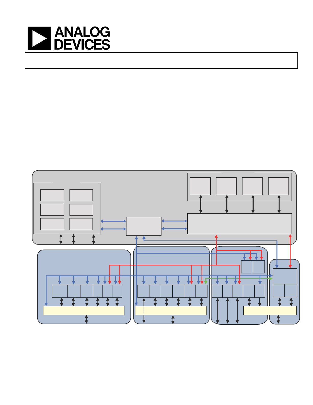
SHARC Processor
Internal Memory I/F
Block 0
RAM/ROM
B0D
64-BIT
Instruction
Cache
5 Stage
Sequencer
PEx PEy
PMD
64-BIT
IOD0 32-BIT
EPD BUS 64-BIT
Core Bus
Cross Bar
S/PDIF
Tx/Rx
PCG
A
-
D
DPI Routing/Pins
SPI/B UART
Block 1
RAM/ROM
Block 2
RAM
Block 3
RAM
AMI
SDRAM
CTL
EP
External Port Pin MUX
TIMER
1
-
0
SPORT
7
-
0
ASRC
3-0
PWM
3
-
0
DAG1/2
Core
Timer
PDAP/
IDP
7
-
0
TWI
IOD0 BUS
DTCP/
MTM
PCG
C
-
D
PERIPHERAL BUS 32-BIT
CORE
FLAGS/
PWM3
-
1
JTAG
Internal Memory
DMD
64-BIT
PMD 64-BIT
CORE
FLAGS
IOD1
32-BIT
PERIPHERAL BUS
B1D
64-BIT
B2D
64-BIT
B3D
64-BIT
DPI Peripherals
DAI Peripherals
Peripherals
External
Port
SIMD Core
S
THERMAL
DIODE
FFT
FIR
IIR
MLB
SPEP BUS
DMD
64-BIT
FLAGx/IRQx/
TMREXP
WDT
RTC
SHIFT
REG
DAI Routing/Pins
ADSP-21477/ADSP-21478/ADSP-21479
SUMMARY
High performance 32-bit/40-bit floating-point processor
optimized for high performance audio processing
Single-instruction, multiple-data (SIMD) computational
architecture
On-chip memory—up to 5M bits of on-chip RAM, 4M bits of
on-chip ROM
Up to 300 MHz operating frequency
Qualified for automotive applications. See Automotive Prod-
ucts on Page 74
Code compatible with all other members of the SHARC family
The ADSP-2147x processors are available with unique
audio-centric peripherals, such as the digital applications
interface, serial ports, precision clock generators, S/PDIF
transceiver, asynchronous sample rate converters, input
data port, and more.
Factory programmed ROM versions containing latest audio
decoders from Dolby and DTS, available to IP licenses
For complete ordering information, see Ordering Guide on
Page 75.
SHARC and the SHARC logo are registered trademarks of Analog Devices, Inc.
Rev. B
Information furnished by Analog Devices is believed to be accurate and reliable.
However, no responsibility is assumed by Analog Devices for its use, nor for any
infringements of patents or other rights of third parties that may result from its use.
Specifications subject to change without notice. No license is granted by implication
or otherwise under any patent or patent rights of Analog Devices. Trademarks and
registered trademarks are the property of their respective companies.
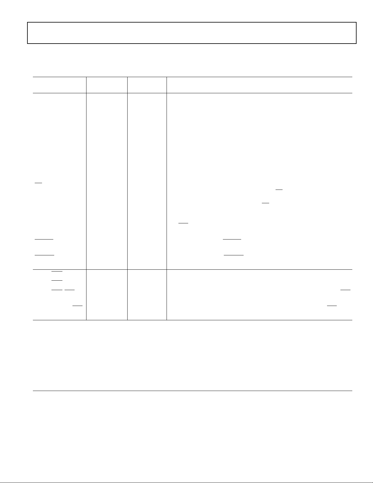
Figure 1. Functional Block Diagram
One Technology Way, P.O. Box 9106, Norwood, MA 02062-9106 U.S.A.
Tel: 781.329.4700 www.analog.com
Fax: 781.326.3113 ©2012 Analog Devices, Inc. All rights reserved.
Page 2

ADSP-21477/ADSP-21478/ADSP-21479
TABLE OF CONTENTS
Summary ............................................................... 1
Product Application Restriction .................................. 2
General Description ................................................. 3
Family Core Architecture ........................................ 4
Family Peripheral Architecture ................................ 8
I/O Processor Features ......................................... 12
System Design .................................................... 13
Development Tools ............................................. 13
Additional Information ........................................ 14
Related Signal Chains .......................................... 14
Pin Function Descriptions ....................................... 15
Specifications ........................................................ 20
Operating Conditions .......................................... 20
Electrical Characteristics ....................................... 21
Maximum Power Dissipation ................................ 23
Package Information ........................................... 23
REVISION HISTORY
3/12—Rev. A to Rev. B
Revised Real Time Clock, SR_LDO and EMU
in Pin Function Descriptions .................................... 15
, t
Corrected t
Sequencing Timing Requirements (Processor Startup) ... . 26
Revised note in Figure 8, 266 MHz Operation (Fundamental
Mode Crystal) ....................................................... 28
Added additional models to:
Automotive Products .............................................. 74
Ordering Guide ..................................................... 75
Added the 88-lead LFCSP_VQ package and the ADSP-21477
model. General information, specifications, and ordering information for this package and model can be found in the
following sections:
ADSP-2147x Family Features ...................................... 3
ADSP-21477 Internal Memory Space, 2M bits . . .............. 6
Operating Conditions ............................................. 20
Core Timer .......................................................... 30
Timer PWM_OUT Cycle Timing .............................. 30
Precision Clock Generator (Direct Pin Routing) ............ 33
Serial Ports ........................................................... 40
Input Data Port (IDP) ............................................. 46
Parallel Data Acquisition Port (PDAP) ........................ 47
Sample Rate Converter—Serial Output Port ................. 49
Pulse-Width Modulation Generators (PWM) ............... 50
PLLRST
timing in Table 19, Power-Up
CLKRST
Pin Descriptions
ESD Sensitivity ................................................... 23
Absolute Maximum Ratings ................................... 23
Timing Specifications ........................................... 24
Output Drive Currents ......................................... 64
Test Conditions .................................................. 64
Capacitive Loading .............................................. 64
Thermal Characteristics ........................................ 65
88-LFCSP_VQ Lead Assignment ................................ 67
100-LQFP_EP Lead Assignment ................................ 69
196-BGA Ball Assignment ........................................ 71
Outline Dimensions ................................................ 72
Surface-Mount Design .......................................... 74
Automotive Products .............................................. 74
Ordering Guide ..................................................... 75
S/PDIF Transmitter Input Data Timing ....................... 53
SPI Interface—Master ............................................. 55
SPI Interface—Slave ................................................ 56
JTAG Test Access Port and Emulation ......................... 63
Thermal Characteristics for 88-Lead LFCSP_VQ ........... 65
88-LFCSP_VQ Lead Assignment ................................ 67
88-Lead Lead Frame Chip Scale Package [LFCSP_VQ]
(CP-88-5) Dimensions Shown in Millimeters ................ 72
Automotive Products .............................................. 74
Ordering Guide ..................................................... 75
PRODUCT APPLICATION RESTRICTION
Not for use in in-vivo applications for body fluid constituent
monitoring, including monitoring one or more of the components that form, or may be a part of, or contaminate human
blood or other body fluids, such as, but not limited to, carboxyhemoglobin, methemoglobin total hemoglobin, oxygen
saturation, oxygen content, fractional arterial oxygen saturation, bilirubin, glucose, drugs, lipids, water, protein, and pH.
Rev. B | Page 2 of 76 | March 2012
Page 3
ADSP-21477/ADSP-21478/ADSP-21479
GENERAL DESCRIPTION
The ADSP-2147x SHARC
SIMD SHARC family of DSPs that feature Analog Devices’
Super Harvard Architecture. The processors are source code
compatible with the ADSP-2126x, ADSP-2136x, ADSP-2137x,
ADSP-2146x, and ADSP-2116x DSPs as well as with first
generation ADSP-2106x SHARC processors in SISD (singleinstruction, single-data) mode. These processors are 32-bit/
40-bit floating-point processors optimized for high performance audio applications with a large on-chip SRAM, multiple
internal buses to eliminate I/O bottlenecks, and an innovative
digital applications interface (DAI).
Table 1 shows performance benchmarks for the ADSP-2147x
processors. Table 2 shows the features of the individual product
offerings.
Table 1. Processor Benchmarks
Benchmark Algorithm
1024 Point Complex FFT
(Radix 4, with Reversal)
FIR Filter (per Tap)
IIR Filter (per Biquad)
Matrix Multiply (Pipelined)
[3 × 3] × [3 × 1]
[4 × 4] × [4 × 1]
Divide (y/×) 11.61 ns 17.41 ns
Inverse Square Root 18.08 ns 27.12 ns
1
Assumes two files in multichannel SIMD mode.
Table 2. ADSP-2147x Family Features
®
processors are members of the
Speed
(at 300 MHz)
Speed
(at 200 MHz)
30.59 s 45.885 s
1
1
1.66 ns 2.49 ns
6.65 ns 9.975 ns
14.99 ns
26.66 ns
22.485 ns
39.99 ns
Table 2. ADSP-2147x Family Features (Continued)
Feature
Watch Dog Timer
Real-Time Clock2,
Shift Register
2
2
3
ADSP-21477
ADSP-21478
No Yes
No Yes
No Yes
IDP/PDAP Yes
UART 1
DAI (SRU)/DPI (SRU2) 20/14 Pins
S/PDIF Transceiver 1
SPI 2
TWI 1
SRC SNR Performance –128 dB
Thermal Diode
4
Ye s
VISA Support Yes
100-Lead
LQFP
Package
1
The 100-lead and 88-lead packages of the processors do not contain an external
2
Available on the 196-ball CSP_BGA package only.
3
Real Time Clock (RTC) is supported only for products with a temperature range
4
Available on the 88-lead and 100-lead packages only.
1
port. The SDRAM controller pins must be disabled when using this package.
For more information, see Pin Function Descriptions on Page 16.
of 0°C to +70°C and not supported for all other temperature grades.
88-Lead
LFCSP_VQ
196-Ball CSP_BGA
100-Lead LQFP
88-lead LFCSP_VQ
ADSP-21479
Feature
ADSP-21477
ADSP-21478
Frequency 200 MHz Up to 300 MHz
RAM 2M bits 3M bits 5M bits
ROM N/A 4M bits
4 units (3 in 100-lead
Pulse-Width Modulation 3
External Port Interface
(SDRAM, AMI)
1
No Yes, 16-Bit
package)
Serial Ports 8
Direct DMA from SPORTs
to External Memory No Yes
FIR, IIR, FFT Accelerator Yes
Automotive models
MediaLB Interface No
only
Rev. B | Page 3 of 76 | March 2012
The diagram on Page 1 shows the two clock domains (core and
ADSP-21479
I/O processor) that make up the ADSP-2147x processors. The
core clock domain contains the following features.
• Two processing elements (PEx, PEy), each of which comprises an ALU, multiplier, shifter, and data register file
• Two data address generators (DAG1, DAG2)
• A program sequencer with instruction cache
• PM and DM buses capable of supporting 2 × 64-bit data
transfers between memory and the core at every core processor cycle
• One periodic interval timer with pinout
• On-chip SRAM (up to 5M bit)
• A JTAG test access port for emulation and boundary scan.
The JTAG provides software debug through user breakpoints, which allows flexible exception handling.
Page 4

ADSP-21477/ADSP-21478/ADSP-21479
The block diagram of the ADSP-2147x on Page 1 also shows the
peripheral clock domain (also known as the I/O processor),
which contains the following features:
•IOD0 (peripheral DMA) and IOD1 (external port DMA)
buses for 32-bit data transfers
• Peripheral and external port buses for core connection
• External port with an asynchronous memory interface
(AMI) and SDRAM controller
•4 units for pulse width modulation (PWM) control
• 1 memory-to-memory (MTM) unit for internal-to-internal
memory transfers
• Digital applications interface that includes four precision
clock generators (PCG), an input data port (IDP/PDAP)
for serial and parallel interconnect, an S/PDIF
receiver/transmitter, four asynchronous sample rate converters, eight serial ports, a shift register, and a flexible
signal routing unit (DAI SRU).
• Digital peripheral interface that includes two timers, a 2wire interface, one UART, two serial peripheral interfaces
(SPI), two precision clock generators (PCG), three pulse
width modulation (PWM) units, and a flexible signal routing unit (DPI SRU).
As shown in the SHARC core block diagram on Page 5, the processors use two computational units to deliver a significant
performance increase over the previous SHARC processors on a
range of DSP algorithms. With its SIMD computational hardware, the processors can perform 1.8 GFLOPS running at
300 MHz.
FAMILY CORE ARCHITECTURE
The processors are code compatible at the assembly level with
the ADSP-2146x, ADSP-2137x, ADSP-2136x, ADSP-2126x,
ADSP-21160, and ADSP-21161, and with the first generation
ADSP-2106x SHARC processors. The ADSP-2147x share architectural features with the ADSP-2126x, ADSP-2136x, ADSP2137x, ADSP-2146x, and ADSP-2116x SIMD SHARC processors, as shown in Figure 2 and detailed in the following sections.
SIMD Computational Engine
The processors contain two computational processing elements
that operate as a single-instruction, multiple-data (SIMD)
engine. The processing elements are referred to as PEX and PEY
and each contains an ALU, multiplier, shifter, and register file.
PEX is always active, and PEY may be enabled by setting the
PEYEN mode bit in the MODE1 register. SIMD mode allows
the processor to execute the same instruction in both processing
elements, but each processing element operates on different
data. This architecture is efficient at executing math intensive
DSP algorithms.
SIMD mode also affects the way data is transferred between
memory and the processing elements because twice the data
bandwidth is required to sustain computational operation in the
processing elements. Therefore, entering SIMD mode also doubles the bandwidth between memory and the processing
elements. When using the DAGs to transfer data in SIMD
mode, two data values are transferred with each memory or register file access.
SIMD mode is supported from external SDRAM but is not supported in the AMI.
Independent, Parallel Computation Units
Within each processing element is a set of computational units.
The computational units consist of an arithmetic/logic unit
(ALU), multiplier, and shifter. These units perform all operations in a single cycle. The three units within each processing
element are arranged in parallel, maximizing computational
throughput. Single multifunction instructions execute parallel
ALU and multiplier operations. In SIMD mode, the parallel
ALU and multiplier operations occur in both processing elements. These computation units support IEEE 32-bit singleprecision floating-point, 40-bit extended precision floatingpoint, and 32-bit fixed-point data formats.
Timer
The processor contains a core timer that can generate periodic
software interrupts. The core timer can be configured to use
FLAG3 as a timer expired signal.
Data Register File
Each processing element contains a general-purpose data register file. The register files transfer data between the computation
units and the data buses, and store intermediate results. These
10-port, 32-register (16 primary, 16 secondary) register files,
combined with the processor’s enhanced Harvard architecture,
allow unconstrained data flow between computation units and
internal memory. The registers in PEX are referred to as
R0–R15 and in PEY as S0–S15.
Context Switch
Many of the processor’s registers have secondary registers that
can be activated during interrupt servicing for a fast context
switch. The data registers in the register file, the DAG registers,
and the multiplier result registers all have secondary registers.
The primary registers are active at reset, while the secondary
registers are activated by control bits in a mode control register.
Universal Registers
Universal registers can be used for general-purpose tasks. The
USTAT (4) registers allow easy bit manipulations (Set, Clear,
Toggle, Test, XOR) for all peripheral control and status
registers.
The data bus exchange register (PX) permits data to be passed
between the 64-bit PM data bus and the 64-bit DM data bus, or
between the 40-bit register file and the PM/DM data bus. These
registers contain hardware to handle the data width difference.
Single-Cycle Fetch of Instruction and Four Operands
The processors feature an enhanced Harvard architecture in
which the data memory (DM) bus transfers data and the program memory (PM) bus transfers both instructions and data
(see Figure 2). With its separate program and data memory
Rev. B | Page 4 of 76 | March 2012
Page 5
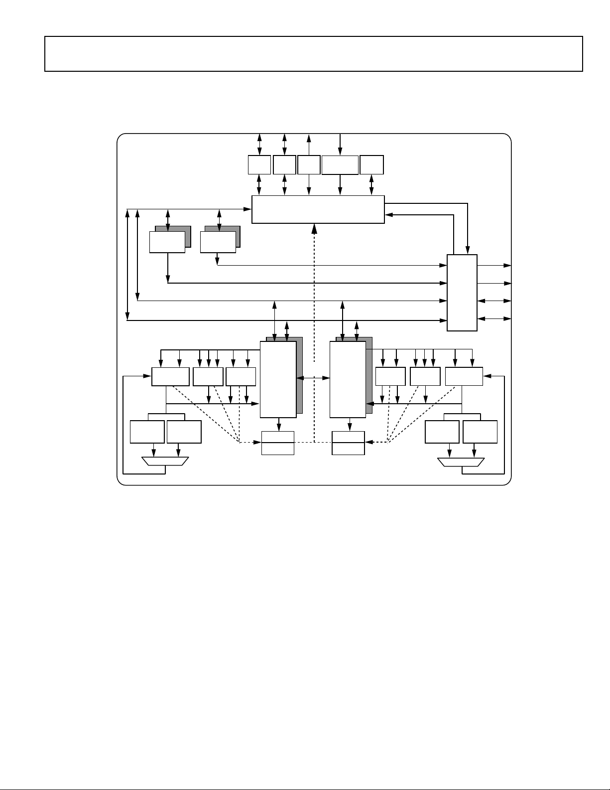
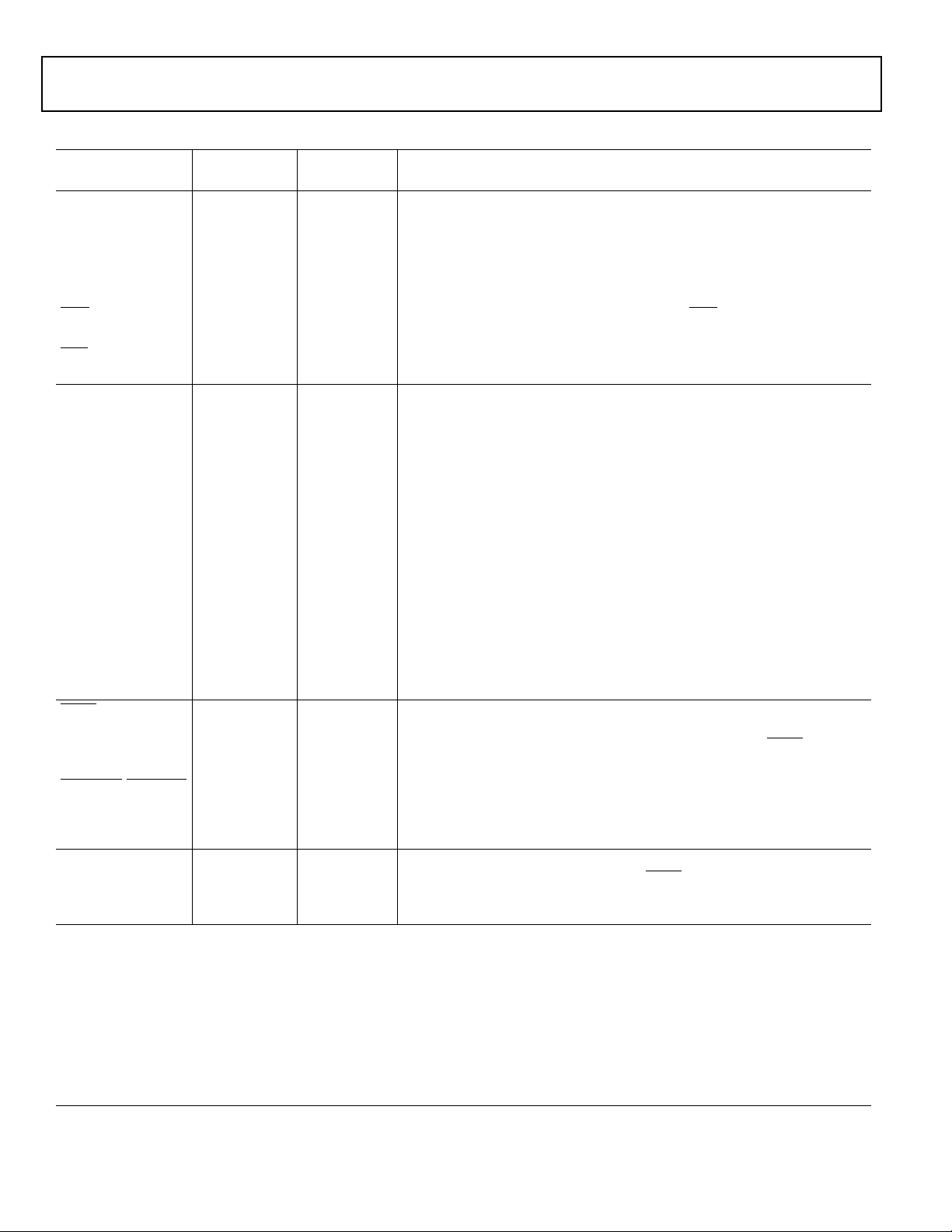
ADSP-21477/ADSP-21478/ADSP-21479
S
SIMD Core
CACHEINTERRUPT
5 STAGE
PROGRAM SEQUENCER
PM ADDRESS 32
DM ADDRESS 32
DM DATA 64
PM DATA 64
DAG1
16×32
MRF
80-BIT
ALU
MULTIPLIER
SHIFTER
RF
Rx/Fx
PEx
16×40-BIT
JTAG
DMD/PMD 64
ASTATx
STYKx
ASTATy
STYKy
TIMER
RF
Sx/SFx
PEy
16×40-BIT
MRB
80-BIT
MSB
80-BIT
MSF
80-BIT
FLAG
SYSTEM
I/F
US TAT
4×32-BIT
PX
64-BIT
DAG2
16×32
ALU
MULTIPLIER
SHIFTER
DATA
SWAP
PM ADDRESS 24
PM DATA 48
buses and on-chip instruction cache, the processor can simultaneously fetch four operands (two over each data bus) and one
instruction (from the cache), all in a single cycle.
Instruction Cache
The processor includes an on-chip instruction cache that
enables three-bus operation for fetching an instruction and four
data values. The cache is selective—only the instructions whose
fetches conflict with PM bus data accesses are cached. This
cache allows full speed execution of core looped operations such
as digital filter multiply-accumulates, and FFT butterfly
processing.
Data Address Generators with Zero-Overhead Hardware Circular Buffer Support
The processor’s two data address generators (DAGs) are used
for indirect addressing and implementing circular data buffers
in hardware. Circular buffers allow efficient programming of
delay lines and other data structures required in digital signal
processing, and are commonly used in digital filters and Fourier
transforms. The two DAGs of the processors contain sufficient
registers to allow the creation of up to 32 circular buffers (16
Figure 2. SHARC Core Block Diagram
Rev. B | Page 5 of 76 | March 2012
primary register sets, 16 secondary). The DAGs automatically
handle address pointer wraparound, reduce overhead, increase
performance, and simplify implementation. Circular buffers can
start and end at any memory location.
Flexible Instruction Set
The 48-bit instruction word accommodates a variety of parallel
operations, for concise programming. For example, the
processors can conditionally execute a multiply, an add, and a
subtract in both processing elements while branching and fetching up to four 32-bit values from memory—all in a single
instruction.
Variable Instruction Set Architecture (VISA)
In addition to supporting the standard 48-bit instructions from
previous SHARC processors, the processors support new
instructions of 16 and 32 bits. This feature, called Variable
Instruction Set Architecture (VISA), drops redundant/unused
Page 6
ADSP-21477/ADSP-21478/ADSP-21479
bits within the 48-bit instruction to create more efficient and
compact code. The program sequencer supports fetching these
16-bit and 32-bit instructions from both internal and external
SDRAM memory. This support is not extended to the asynchronous memory interface (AMI). Source modules need to be built
using the VISA option, in order to allow code generation tools
to create these more efficient opcodes.
On-Chip Memory
The processors contain varying amounts of internal RAM and
internal ROM which is shown in Table 3 through Table 5. Each
block can be configured for different combinations of code and
data storage. Each memory block supports single-cycle, independent accesses by the core processor and I/O processor.
The processor’s SRAM can be configured as a maximum of
160k words of 32-bit data, 320k words of 16-bit data, 106.7k
words of 48-bit instructions (or 40-bit data), or combinations of
different word sizes up to 5M bits. All of the memory can be
accessed as 16-bit, 32-bit, 48-bit, or 64-bit words. A 16-bit
Table 3. ADSP-21477 Internal Memory Space, 2M bits
IOP Registers 0x0000 0000–0x0003 FFFF
Extended Precision Normal or
Long Word (64 Bits)
Block 0 ROM (Reserved)
0x0004 0000–0x0004 7FFF
Reserved
0x0004 8000–0x0004 8FFF
Block 0 SRAM
0x0004 9000–0x0004 BFFF
Reserved
0x0004 C000–0x0004 FFFF
Block 1 ROM (Reserved)
0x0005 0000–0x0005 7FFF
Reserved
0x0005 8000–0x0005 8FFF
Block 1 SRAM
0x0005 9000–0x0005 BFFF
Reserved
0x0005 C000–0x0005 FFFF
Block 2 SRAM
0x0006 0000–0x0006 0FFF
Reserved
0x0006 1000– 0x0006 FFFF
Block 3 SRAM
0x0007 0000–0x0007 0FFF
Reserved
0x0007 1000–0x0007 FFFF
Instruction Word (48 Bits) Normal Word (32 Bits) Short Word (16 Bits)
Block 0 ROM (Reserved)
0x0008 0000–0x0008 AAA9
Reserved
0x0008 AAAA–0x0008 BFFF
Block 0 SRAM
0x0008 C000–0x0008 FFFF
Reserved
0x0009 000–0x0009 5554
Block 1 ROM (Reserved)
0x000A 0000–0x000A AAA9
Reserved
0x000A AAAA–0x000A BFFF
Block 1 SRAM
0x000A C000–0x000A FFFF
Reserved
0x000B 0000–0x000B 5554
Block 2 SRAM
0x000C 0000–0x000C 1554
Reserved
0x000C 1555–0x000D 5554
Block 3 SRAM
0x000E 0000–0x000E 1554
Reserved
0x000E 1555–0x000F 5554
floating-point storage format is supported that effectively doubles the amount of data that may be stored on-chip. Conversion
between the 32-bit floating-point and 16-bit floating-point
formats is performed in a single instruction. While each memory block can store combinations of code and data, accesses are
most efficient when one block stores data using the DM bus for
transfers, and the other block stores instructions and data using
the PM bus for transfers.
Using the DM bus and PM buses, with one bus dedicated to a
memory block, assures single-cycle execution with two data
transfers. In this case, the instruction must be available in the
cache.
The memory maps in Table 3 through Table 5 display the internal memory address space of the processors. The 48-bit space
section describes what this address range looks like to an
instruction that retrieves 48-bit memory. The 32-bit section
describes what this address range looks like to an instruction
that retrieves 32-bit memory.
Block 0 ROM (Reserved)
0x0008 0000–0x0008 FFFF
Reserved
0x0009 0000–0x0009 1FFF
Block 0 SRAM
0x0009 2000–0x0009 7FFF
Reserved
0x0009 8000–0x0009 FFFF
Block 1 ROM (Reserved)
0x000A 0000–0x000AFFFF
Reserved
0x000B 0000–0x000B 1FFF
Block 1 SRAM
0x000B 2000–0x000B 7FFF
Reserved
0x000B 8000–0x000B FFFF
Block 2 SRAM
0x000C 0000–0x000C 1FFF
Reserved
0x000C 2000–0x000D FFFF
Block 3 SRAM
0x000E 0000–0x000E 1FFF
Reserved
0x000E 2000–0x000F FFFF
Block 0 ROM (Reserved)
0x0010 0000–0x0011 FFFF
Reserved
0x0012 0000–0x0012 FFFF
Block 0 SRAM
0x0012 4000–0x0012 FFFF
Reserved
0x0013 0000–0x0013 FFFF
Block 1 ROM (Reserved)
0x0014 0000–0x0015 FFFF
Reserved
0x0016 0000–0x0016 3FFF
Block 1 SRAM
0x0016 4000–0x0016 FFFF
Reserved
0x0017 0000–0x0017 FFFF
Block 2 SRAM
0x0018 0000–0x0018 3FFF
Reserved
0x0018 4000–0x001B FFFF
Block 3 SRAM
0x001C 0000–0x001C 3FFF
Reserved
0x001C 4000–0x001F FFFF
Rev. B | Page 6 of 76 | March 2012
Page 7
ADSP-21477/ADSP-21478/ADSP-21479
Table 4. ADSP-21478 Internal Memory Space (3M bits)
IOP Registers 0x0000 0000–0x0003 FFFF
Extended Precision Normal or
Long Word (64 Bits)
Block 0 ROM (Reserved)
0x0004 0000–0x0004 7FFF
Reserved
0x0004 8000–0x0004 8FFF
Block 0 SRAM
0x0004 9000–0x0004 CFFF
Reserved
0x0004 D000–0x0004 FFFF
Block 1 ROM (Reserved)
0x0005 0000–0x0005 7FFF
Reserved
0x0005 8000–0x0005 8FFF
Block 1 SRAM
0x0005 9000–0x0005 CFFF
Reserved
0x0005 D000–0x0005 FFFF
Block 2 SRAM
0x0006 0000–0x0006 1FFF
Reserved
0x0006 2000– 0x0006 FFFF
Block 3 SRAM
0x0007 0000–0x0007 1FFF
Reserved
0x0007 2000–0x0007 FFFF
1
Some processors include a customer-definable ROM block. ROM addresses on these models are not reserved as shown in this table. Please contact your Analog Devices sales
representative for additional details.
Instruction Word (48 Bits) Normal Word (32 Bits) Short Word (16 Bits)
Block 0 ROM (Reserved)
0x0008 0000–0x0008 AAA9
Reserved
0x0008 AAAA–0x0008 BFFF
Block 0 SRAM
0x0008 C000–0x0009 1554
Reserved
0x0009 1555–0x0009 FFFF
Block 1 ROM (Reserved)
0x000A 0000–0x000A AAA9
Reserved
0x000A AAAA–0x000A BFFF
Block 1 SRAM
0x000A C000–0x000B 1554
Reserved
0x000B 1555–0x000B FFFF
Block 2 SRAM
0x000C 0000–0x000C 2AA9
Reserved
0x000C 2AAA–0x000D FFFF
Block 3 SRAM
0x000E 0000–0x000E 2AA9
Reserved
0x000E 2AAA–0x000F FFFF
1
Block 0 ROM (Reserved)
0x0008 0000–0x0008 FFFF
Reserved
0x0009 0000–0x0009 1FFF
Block 0 SRAM
0x0009 2000–0x0009 9FFF
Reserved
0x0009 A000–0x0009 FFFF
Block 1 ROM (Reserved)
0x000A 0000–0x000A FFFF
Reserved
0x000B 0000–0x000B 1FFF
Block 1 SRAM
0x000B 2000–0x000B 9FFF
Reserved
0x000B A000–0x000B FFFF
Block 2 SRAM
0x000C 0000–0x000C 3FFF
Reserved
0x000C 4000–0x000D FFFF
Block 3 SRAM
0x000E 0000–0x000E 3FFF
Reserved
0x000E 4000–0x000F FFFF
Block 0 ROM (Reserved)
0x0010 0000–0x0011 FFFF
Reserved
0x0012 0000–0x0012 3FFF
Block 0 SRAM
0x0012 4000–0x0013 3FFF
Reserved
0x0013 4000–0x0013 FFFF
Block 1 ROM (Reserved)
0x0014 0000–0x0015 FFFF
Reserved
0x0016 0000–0x0016 3FFF
Block 1 SRAM
0x0016 4000–0x0017 3FFF
Reserved
0x0017 4000–0x0017 FFFF
Block 2 SRAM
0x0018 0000–0x0018 7FFF
Reserved
0x0018 8000–0x001B FFFF
Block 3 SRAM
0x001C 0000–0x001C 7FFF
Reserved
0x001C 8000–0x001F FFFF
Rev. B | Page 7 of 76 | March 2012
Page 8
ADSP-21477/ADSP-21478/ADSP-21479
Table 5. ADSP-21479 Internal Memory Space (5M bits)
IOP Registers 0x0000 0000–0x0003 FFFF
Extended Precision Normal or
Long Word (64 Bits)
Block 0 ROM (Reserved)
0x0004 0000–0x0004 7FFF
Reserved
0x0004 8000–0x0004 8FFF
Block 0 SRAM
0x0004 9000–0x0004 EFFF
Reserved
0x0004 F000–0x0004 FFFF
Block 1 ROM (Reserved)
0x0005 0000–0x0005 7FFF
Reserved
0x0005 8000–0x0005 8FFF
Block 1 SRAM
0x0005 9000–0x0005 EFFF
Reserved
0x0005 F000–0x0005 FFFF
Block 2 SRAM
0x0006 0000–0x0006 3FFF
Reserved
0x0006 4000– 0x0006 FFFF
Block 3 SRAM
0x0007 0000–0x0007 3FFF
Reserved
0x0007 4000–0x0007 FFFF
1
Some processors include a customer-definable ROM block. ROM addresses on these models are not reserved as shown in this table. Please contact your Analog Devices sales
representative for additional details.
Instruction Word (48 Bits) Normal Word (32 Bits) Short Word (16 Bits)
Block 0 ROM (Reserved)
0x0008 0000–0x0008 AAA9
Reserved
0x0008 AAAA–0x0008 BFFF
Block 0 SRAM
0x0008 C000–0x0009 3FFF
Reserved
0x0009 4000–0x0009 FFFF
Block 1 ROM (Reserved)
0x000A 0000–0x000A AAA9
Reserved
0x000A AAAA–0x000A BFFF
Block 1 SRAM
0x000A C000–0x000B 3FFF
Reserved
0x000B 4000–0x000B FFFF
Block 2 SRAM
0x000C 0000–0x000C 5554
Reserved
0x000C 5555–0x0000D FFFF
Block 3 SRAM
0x000E 0000–0x000E 5554
Reserved
0x000E 5555–0x0000F FFFF
1
Block 0 ROM (Reserved)
0x0008 0000–0x0008 FFFF
Reserved
0x0009 0000–0x0009 1FFF
Block 0 SRAM
0x0009 2000–0x0009 DFFF
Reserved
0x0009 E000–0x0009 FFFF
Block 1 ROM (Reserved)
0x000A 0000–0x000AFFFF
Reserved
0x000B 0000–0x000B 1FFF
Block 1 SRAM
0x000B 2000–0x000B DFFF
Reserved
0x000B E000–0x000B FFFF
Block 2 SRAM
0x000C 0000–0x000C 7FFF
Reserved
0x000C 8000–0x000D FFFF
Block 3 SRAM
0x000E 0000–0x000E 7FFF
Reserved
0x000E 8000–0x000F FFFF
Block 0 ROM (Reserved)
0x0010 0000–0x0011 FFFF
Reserved
0x0012 0000–0x0012 3FFF
Block 0 SRAM
0x0012 4000–0x0013 BFFF
Reserved
0x0013 C000–0x0013 FFFF
Block 1 ROM (Reserved)
0x0014 0000–0x0015 FFFF
Reserved
0x0016 0000–0x0016 3FFF
Block 1 SRAM
0x0016 4000–0x0017 BFFF
Reserved
0x0017 C000–0x0017 FFFF
Block 2 SRAM
0x0018 0000–0x0018 FFFF
Reserved
0x0019 0000–0x001B FFFF
Block 3 SRAM
0x001C 0000–0x001C FFFF
Reserved
0x001D 0000–0x001F FFFF
On-Chip Memory Bandwidth
The internal memory architecture allows programs to have four
accesses at the same time to any of the four blocks (assuming
there are no block conflicts). The total bandwidth is realized
using the DMD and PMD buses (2 × 64-bit at CCLK speed) and
the IOD0/1 buses (2 × 32-bit at PCLK speed).
ROM Based Security
The processors have a ROM security feature that provides hardware support for securing user software code by preventing
unauthorized reading from the internal code. When using this
feature, the processors do not boot-load any external code, executing exclusively from internal ROM. Additionally, the
processor is not freely accessible via the JTAG port. Instead, a
unique 64-bit key, which must be scanned in through the JTAG
or Test Access Port, is assigned to each customer. The device
ignores an incorrect key. Emulation features are available after
the correct key is scanned.
Rev. B | Page 8 of 76 | March 2012
Digital Transmission Content Protection
The DTCP specification defines a cryptographic protocol for
protecting audio entertainment content from illegal copying,
intercepting, and tampering as it traverses high performance
digital buses, such as the IEEE 1394 standard. Only legitimate
entertainment content delivered to a source device via another
approved copy protection system (such as the DVD content
scrambling system) is protected by this copy protection system.
For more information on this feature, contact your local ADI
sales office.
FAMILY PERIPHERAL ARCHITECTURE
The ADSP-2147x family contains a rich set of peripherals that
support a wide variety of applications including high quality
audio, medical imaging, communications, military, test equipment, 3D graphics, speech recognition, motor control, imaging,
and other applications.
Page 9
ADSP-21477/ADSP-21478/ADSP-21479
External Memory
The external memory interface supports access to the external
memory through core and DMA accesses. The external memory
address space is divided into four banks. Any bank can be programmed as either asynchronous or synchronous memory. The
external ports are comprised of the following modules.
• An AMI which communicates with SRAM, FLASH, and
other devices that meet the standard asynchronous SRAM
access protocol. The AMI supports 6M words of external
memory in Bank 0 and 8M words of external memory in
Bank 1, Bank 2, and Bank 3.
• An SDRAM controller that supports a glueless interface
with any of the standard SDRAMs. The SDC supports 62M
words of external memory in Bank 0, and 64M words of
external memory in Bank 1, Bank 2, and Bank 3.
• Arbitration logic to coordinate core and DMA transfers
between internal and external memory over the
external port.
External Port
The external port provides a high performance, glueless interface to a wide variety of industry-standard memory devices. The
external port, available on the 196-ball CSP_BGA, may be used
to interface to synchronous and/or asynchronous memory
devices through the use of its separate internal memory controllers. The first is an SDRAM controller for connection of
industry-standard synchronous DRAM devices while the second is an asynchronous memory controller intended to
interface to a variety of memory devices. Four memory select
pins enable up to four separate devices to coexist, supporting
any desired combination of synchronous and asynchronous
device types. Non-SDRAM external memory address space is
shown in Table 6.
Table 6. External Memory for Non-SDRAM Addresses
Size in
Bank
Bank 0 6M 0x0020 0000–0x007F FFFF
Bank 1 8M 0x0400 0000–0x047F FFFF
Bank 2 8M 0x0800 0000–0x087F FFFF
Bank 3 8M 0x0C00 0000–0x0C7F FFFF
SIMD Access to External Memory
The SDRAM controller supports SIMD access on the 64-bit
external port data bus (EPD) which allows access to the complementary registers on the PEy unit in the normal word space
(NW). This improves performance since there is no need to
explicitly load the complementary registers (as in SISD mode).
VISA and ISA Access to External Memory
The SDRAM controller supports VISA code operation which
reduces the memory load since the VISA instructions are compressed. Moreover, bus fetching is reduced because, in the best
case, one 48-bit fetch contains three valid instructions. Code
execution from the traditional ISA operation is also supported.
Words Address Range
Note that code execution is only supported from Bank 0 regardless of VISA/ISA. Table 7 shows the address ranges for
instruction fetch in each mode.
Table 7. External Bank 0 Instruction Fetch
Size in
Access Type
ISA (NW) 4M 0x0020 0000–0x005F FFFF
VISA (SW) 10M 0x0060 0000–0x00FF FFFF
Words Address Range
SDRAM Controller
The SDRAM controller, available on the ADSP-2147x in the
196-ball CSP_BGA package, provides an interface of up to four
separate banks of industry-standard SDRAM devices or
DIMMs, at speeds up to f
SDRAM standard, each bank has its own memory select line
–MS3), and can be configured to contain between
(MS0
4 Mbytes and 256 Mbytes of memory. SDRAM external memory address space is shown in Table 8.
Table 8. External Memory for SDRAM Addresses
Size in
Bank
Bank 0 62M 0x0020 0000–0x03FF FFFF
Bank 1 64M 0x0400 0000–0x07FF FFFF
Bank 2 64M 0x0800 0000–0x0BFF FFFF
Bank 3 64M 0x0C00 0000–0x0FFF FFFF
A set of programmable timing parameters is available to configure the SDRAM banks to support slower memory devices. The
SDRAM and the AMI interface do not support 32-bit wide
devices.
The SDRAM controller address, data, clock, and control pins
can drive loads up to distributed 30 pF. For larger memory systems, the SDRAM controller external buffer timing should be
selected and external buffering should be provided so that the
load on the SDRAM controller pins does not exceed 30 pF.
Note that the external memory bank addresses shown are for
normal-word (32-bit) accesses. If 48-bit instructions as well as
32-bit data are both placed in the same external memory bank,
care must be taken while mapping them to avoid overlap.
Words Address Range
. Fully compliant with the
SDCLK
Asynchronous Memory Controller
The asynchronous memory controller, available on the
ADSP-2147x in the 196-ball CSP_BGA package, provides a configurable interface for up to four separate banks of memory or
I/O devices. Each bank can be independently programmed with
different timing parameters, enabling connection to a wide variety of memory devices including SRAM, flash, and EPROM, as
well as I/O devices that interface with standard memory control
lines. Bank 0 occupies a 6M word window and Banks 1, 2, and 3
Rev. B | Page 9 of 76 | March 2012
Page 10

ADSP-21477/ADSP-21478/ADSP-21479
occupy a 8M word window in the processor’s address space but,
if not fully populated, these windows are not made contiguous
by the memory controller logic.
External Port Throughput
The throughput for the external port, based on 133 MHz clock
and 16-bit data bus, is 88 Mbytes/sec for the AMI and
266 Mbytes/sec for SDRAM.
MediaLB
The automotive models of the processors have an MLB interface
which allows the processor to function as a media local bus
device. It includes support for both 3-pin and 5-pin MLB protocols. It supports speeds up to 1024 FS (49.25M bits/sec,
FS = 48.1 kHz) and up to 31 logical channels, with up to
124 bytes of data per media local bus frame. For a list of automotive products, see Automotive Products on Page 74.
Digital Applications Interface (DAI)
The digital applications interface (DAI) provides the ability to
connect various peripherals to any of the DAI pins
(DAI_P20–1).
Programs make these connections using the signal routing unit
(SRU), shown in Figure 1.
The SRU is a matrix routing unit (or group of multiplexers) that
enables the peripherals provided by the DAI to be interconnected under software control. This allows easy use of the DAI
associated peripherals for a much wider variety of applications
by using a larger set of algorithms than is possible with non configurable signal paths.
The associated peripherals include eight serial ports, four precision clock generators (PCG), a S/PDIF transceiver, four ASRCs,
and an input data port (IDP). The IDP provides an additional
input path to the SHARC core, configurable as either eight
channels of serial data, or a single 20-bit wide synchronous parallel data acquisition port. Each data channel has its own DMA
channel that is independent from the processor’s serial ports.
Serial Ports (SPORTs)
The processors feature eight synchronous serial ports that provide an inexpensive interface to a wide variety of digital and
mixed-signal peripheral devices such as Analog Devices’
AD183x family of audio codecs, ADCs, and DACs. The serial
ports are made up of two data lines, a clock, and frame sync. The
data lines can be programmed to either transmit or receive and
each data line has a dedicated DMA channel.
Serial ports can support up to 16 transmit or 16 receive DMA
channels of audio data when all eight SPORTs are enabled, or
four full duplex TDM streams of 128 channels per frame.
Serial port data can be automatically transferred to and from
on-chip memory/external memory via dedicated DMA channels. Each of the serial ports can work in conjunction with
another serial port to provide TDM support. One SPORT provides two transmit signals while the other SPORT provides the
two receive signals. The frame sync and clock are shared.
Serial ports operate in five modes:
• Standard serial mode
•Multichannel (TDM) mode
2
•I
S mode
2
•Packed I
• Left-justified mode
S/PDIF-Compatible Digital Audio Receiver/Transmitter
The S/PDIF receiver/transmitter has no separate DMA channels. It receives audio data in serial format and converts it into a
bi phase encoded signal. The serial data input to the
receiver/transmitter can be formatted as left justified, I
right-justified with word widths of 16, 18, 20, or 24 bits.
The serial data, clock, and frame sync inputs to the S/PDIF
receiver/transmitter are routed through the signal routing unit
(SRU). They can come from a variety of sources, such as the
SPORTs, external pins, the precision clock generators (PCGs),
and are controlled by the SRU control registers.
Asynchronous Sample Rate Converter (SRC)
The sample rate converter contains four blocks and is the same
core as that used in the AD1896 192 kHz stereo asynchronous
sample rate converter. The SRC block provides up to 128 dB
SNR and is used to perform synchronous or asynchronous sample rate conversion across independent stereo channels, without
using internal processor resources. The four SRC blocks can
also be configured to operate together to convert multichannel
audio data without phase mismatches. Finally, the SRC can be
used to clean up audio data from jittery clock sources such as
the S/PDIF receiver.
Input Data Port
The IDP provides up to eight serial input channels—each with
its own clock, frame sync, and data inputs. The eight channels
are automatically multiplexed into a single 32-bit by eight-deep
FIFO. Data is always formatted as a 64-bit frame and divided
into two 32-bit words. The serial protocol is designed to receive
audio channels in I
mode.
The IDP also provides a parallel data acquisition port (PDAP)
which can be used for receiving parallel data. The PDAP port
has a clock input and a hold input. The data for the PDAP can
be received from DAI pins or from the external port pins. The
PDAP supports a maximum of 20-bit data and four different
packing modes to receive the incoming data.
Precision Clock Generators
The precision clock generators (PCG) consist of four units, each
of which generates a pair of signals (clock and frame sync)
derived from a clock input signal. The units, A B, C, and D are
identical in functionality and operate independently of each
other. The two signals generated by each unit are normally used
as a serial bit clock/frame sync pair.
The outputs of PCG A and B can be routed through the DAI
pins and the outputs of PCG C and D can be driven on to the
DAI as well as the DPI pins.
S mode
2
S, left-justified sample pair, or right-justified
2
S or
Rev. B | Page 10 of 76 | March 2012
Page 11

ADSP-21477/ADSP-21478/ADSP-21479
Digital Peripheral Interface (DPI)
The digital peripheral interface provides connections to two
serial peripheral interface ports (SPI), one universal asynchronous receiver-transmitter (UART), 12 flags, a 2-wire interface
(TWI), three PWM modules (PWM3–1), and two generalpurpose timers.
Serial Peripheral (Compatible) Interface (SPI)
The SPI is an industry-standard synchronous serial link,
enabling the SPI-compatible port to communicate with other
SPI compatible devices. The SPI consists of two data pins, one
device select pin, and one clock pin. It is a full-duplex synchronous serial interface, supporting both master and slave modes.
The SPI port can operate in a multi-master environment by
interfacing with up to four other SPI-compatible devices, either
acting as a master or slave device. The SPI-compatible peripheral implementation also features programmable baud rate and
clock phase and polarities. The SPI-compatible port uses open
drain drivers to support a multi-master configuration and to
avoid data contention.
UART Port
The processors provide a full-duplex Universal Asynchronous
Receiver/Transmitter (UART) port, which is fully compatible
with PC-standard UARTs. The UART port provides a simplified UART interface to other peripherals or hosts, supporting
full-duplex, DMA-supported, asynchronous transfers of serial
data. The UART also has multiprocessor communication capability using 9-bit address detection. This allows it to be used in
multidrop networks through the RS-485 data interface
standard. The UART port also includes support for 5 to 8 data
bits, 1 or 2 stop bits, and none, even, or odd parity. The UART
port supports two modes of operation:
• PIO (programmed I/O) – The processor sends or receives
data by writing or reading I/O-mapped UART registers.
The data is double-buffered on both transmit and receive.
• DMA (direct memory access) – The DMA controller transfers both transmit and receive data. This reduces the
number and frequency of interrupts required to transfer
data to and from memory. The UART has two dedicated
DMA channels, one for transmit and one for receive. These
DMA channels have lower default priority than most DMA
channels because of their relatively low service rates.
The UART port's baud rate, serial data format, error code generation and status, and interrupts are programmable:
• Support for bit rates ranging from (f
(f
/16) bits per second.
PCLK
• Support for data formats from 7 to 12 bits per frame.
• Both transmit and receive operations can be configured to
generate maskable interrupts to the processor.
In conjunction with the general-purpose timer functions, autobaud detection is supported.
/1,048,576) to
PCLK
Pulse-Width Modulation
The PWM module is a flexible, programmable, PWM waveform
generator that can be programmed to generate the required
switching patterns for various applications related to motor and
engine control or audio power control. The PWM generator can
generate either center-aligned or edge-aligned PWM waveforms. In addition, it can generate complementary signals on
two outputs in paired mode or independent signals in nonpaired mode (applicable to a single group of four PWM
waveforms).
The entire PWM module has four groups of four PWM outputs
generating 16 PWM outputs in total. Each PWM group produces two pairs of PWM signals on the four PWM outputs.
The PWM generator is capable of operating in two distinct
modes while generating center-aligned PWM waveforms: single
update mode or double update mode. In single update mode the
duty cycle values are programmable only once per PWM period.
This results in PWM patterns that are symmetrical about the
midpoint of the PWM period. In double update mode, a second
updating of the PWM registers is implemented at the midpoint
of the PWM period. In this mode, it is possible to produce
asymmetrical PWM patterns that produce lower harmonic distortion in three-phase PWM inverters.
PWM signals can be mapped to the external port address lines
or to the DPI pins.
Ti me rs
The processors have a total of three timers: a core timer that can
generate periodic software interrupts and two general-purpose
timers that can generate periodic interrupts and be independently set to operate in one of three modes:
•Pulse waveform generation mode
•Pulse width count/capture mode
• External event watch dog mode
The core timer can be configured to use FLAG3 as a timer
expired signal, and the general-purpose timers have one bidirectional pin and four registers that implement its mode of
operation: a 6-bit configuration register, a 32-bit count register,
a 32-bit period register, and a 32-bit pulse width register. A single control and status register enables or disables the generalpurpose timer.
2-Wire Interface Port (TWI)
The TWI is a bidirectional 2-wire serial bus used to move 8-bit
data while maintaining compliance with the I
The TWI master incorporates the following features:
• 7-bit addressing
• Simultaneous master and slave operation on multiple
device systems with support for multi-master data
arbitration
• Digital filtering and timed event processing
• 100 kbps and 400 kbps data rates
• Low interrupt rate
2
C bus protocol.
Rev. B | Page 11 of 76 | March 2012
Page 12

ADSP-21477/ADSP-21478/ADSP-21479
Shift Register
The shift register can be used as a serial to parallel data converter. The shift register module consists of an 18-stage serial
shift register, 18-bit latch, and three-state output buffers. The
shift register and latch have separate clocks. Data is shifted into
the serial shift register on the positive-going transitions of the
shift register serial clock (SR_SCLK) input. The data in each
flip-flop is transferred to the respective latch on a positive-going
transition of the shift register latch clock (SR_LAT) input.
The shift register’s signals can be configured as follows.
• The SR_SCLK can come from any of the SPORT0–7 SCLK
outputs, PCGA/B clock, any of the DAI pins (1–8), and one
dedicated pin (SR_SCLK).
• The SR_LAT can come from any of SPORT0–7 frame sync
outputs, PCGA/B frame sync, any of the DAI pins (1–8),
and one dedicated pin (SR_LAT).
• The SR_SDI input can from any of SPORT0–7 serial data
outputs, any of the DAI pins (1–8), and one dedicated pin
(SR_SDI).
Note that the SR_SCLK, SR_LAT, and SR_SDI inputs must
come from same source except in the case of where SR_SCLK
comes from PCGA/B or SR_SCLK and SR_LAT come from
PCGA/B.
If SR_SCLK comes from PCGA/B, then SPORT0–7 generates
the SR_LAT and SR_SDI signals. If SR_SCLK and SR_LAT
come from PCGA/B, then SPORT0–7 generates the
SR_SDI signal.
I/O PROCESSOR FEATURES
The I/O processor provides up to 65 channels of DMA as well as
an extensive set of peripherals.
DMA Controller
The DMA controller operates independently and invisibly to
the processor core, allowing DMA operations to occur while the
core is simultaneously executing its program instructions. DMA
transfers can occur between the processor’s internal memory
and its serial ports, the SPI-compatible (serial peripheral interface) ports, the IDP (input data port), the parallel data
acquisition port (PDAP) or the UART.
Up to 65 channels of DMA are available on the processors as
shown in Table 9.
Programs can be downloaded using DMA transfers. Other
DMA features include interrupt generation upon completion of
DMA transfers, and DMA chaining for automatic linked DMA
transfers.
Table 9. DMA Channels
Peripheral DMA Channels
SPORTs 16
PDAP 8
SPI 2
UART 2
Table 9. DMA Channels (Continued)
Peripheral DMA Channels
External Port 2
Accelerators 2
Memory-to-Memory 2
MediaLB
1
Automotive models only.
Delay Line DMA
The processor provides delay line DMA functionality. This
allows processor reads and writes to external delay line buffers
(and therefore to external memory) with limited core
interaction.
Scatter/Gather DMA
The processor provides scatter/gather DMA functionality. This
allows processor DMA reads/writes to/from noncontiguous
memory blocks.
1
31
FFT Accelerator
The FFT accelerator implements radix-2 complex/real input,
complex output FFTs with no core intervention. The FFT accelerator runs at the peripheral clock frequency.
FIR Accelerator
The FIR (finite impulse response) accelerator consists of a 1024
word coefficient memory, a 1024 word deep delay line for the
data, and four MAC units. A controller manages the accelerator.
The FIR accelerator runs at the peripheral clock frequency.
IIR Accelerator
The IIR (infinite impulse response) accelerator consists of a
1440 word coefficient memory for storage of biquad coefficients, a data memory for storing the intermediate data and one
MAC unit. A controller manages the accelerator. The IIR accelerator runs at the peripheral clock frequency.
Watchdog Timer ( WDT)
The processors include a 32-bit watchdog timer that can be used
to implement a software watchdog function. A software watchdog can improve system reliability by forcing the processor to a
known state through generation of a system reset if the timer
expires before being reloaded by software. Software initializes
the count value of the timer, and then enables the timer.
The WDT is used to supervise the stability of the system software. When used in this way, software reloads the WDT in a
regular manner so that the downward counting timer never
expires. An expiring timer then indicates that system software
might be out of control.
The WDT resets both the core and the internal peripherals.
Software must be able to determine if the watch dog was the
source of the hardware reset by interrogating a status bit in the
watch dog timer control register.
Rev. B | Page 12 of 76 | March 2012
Page 13
ADSP-21477/ADSP-21478/ADSP-21479
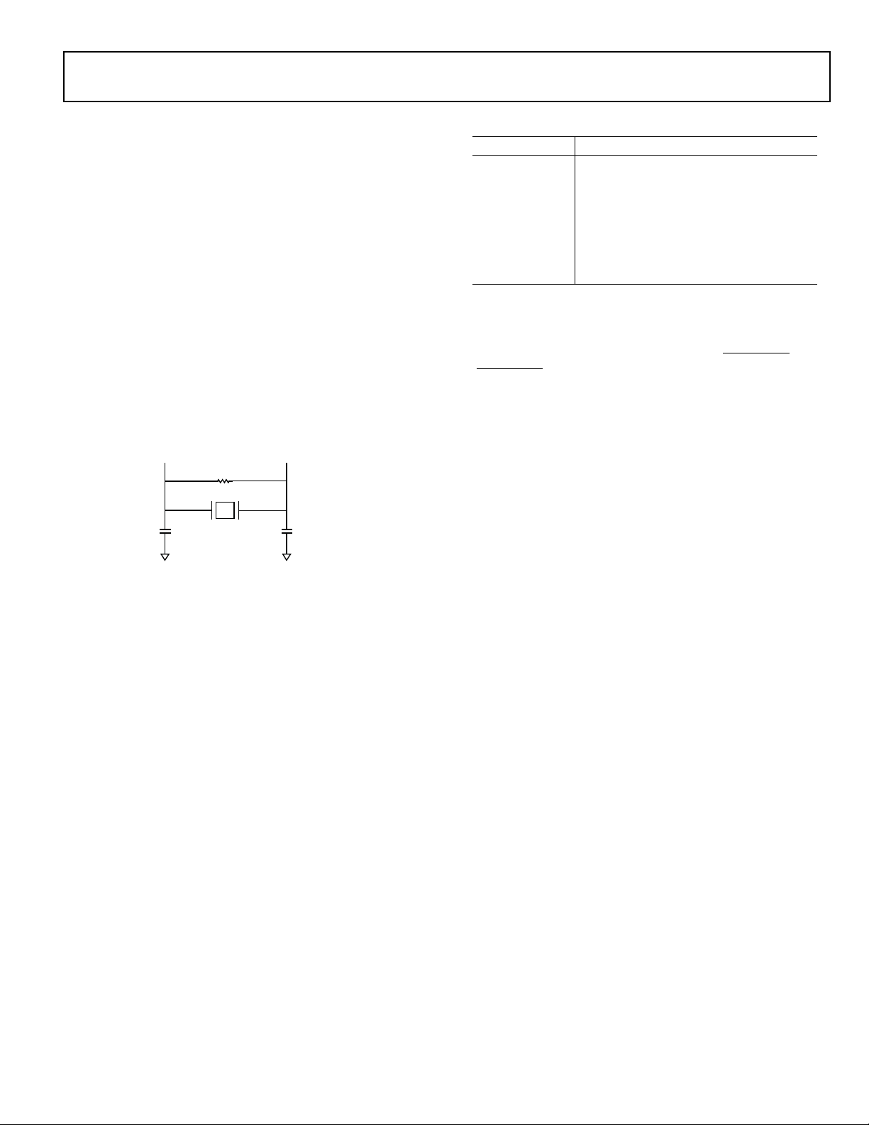
RTXO
C1 C2
X1
NOTE: C1 AND C2 ARE SPECIFIC TO CRYSTAL SPECIFIED FOR X1.
CONTACT CRYSTAL MANUFACTURER FOR DETAI LS. C1 AND C2
SPECIFICATIONS ASSUME BOARD TRACE CAPACIT ANCE OF 3 pF.
RTXI
R1
The watch dog timer also has an internal RC oscillator that can
be used as the clock source. The internal RC oscillator can be
used as an optional alternative to using an external clock applied
to the WDT_CLIN pin.
Real-Time Clock
The real-time clock (RTC) provides a robust set of digital watch
features, including current time, stopwatch, and alarm. The
RTC is clocked by a 32.768 kHz crystal external to the SHARC
processor. Connect RTC pins RTXI and RTXO with external
components as shown in Figure 3.
The RTC peripheral has dedicated power supply pins so that it
can remain powered up and clocked even when the rest of the
processor is in a low power state. The RTC provides several programmable interrupt options, including interrupt per second,
minute, hour, or day clock ticks, interrupt on programmable
stopwatch countdown, or interrupt at a programmed alarm
time. An RTCLKOUT signal that operates at 1 Hz is also provided for calibration.
Figure 3. External Components for RTC
The 32.768 kHz input clock frequency is divided down to a 1 Hz
signal by a prescaler. The counter function of the timer consists
of four counters: a 60-second counter, a 60-minute counter, a
24-hour counter, and a 32,768-day counter. When the alarm
interrupt is enabled, the alarm function generates an interrupt
when the output of the timer matches the programmed value in
the alarm control register. There are two alarms: The first alarm
is for a time of day. The second alarm is for a day and time of
that day.
The stopwatch function counts down from a programmed
value, with one-second resolution. When the stopwatch interrupt is enabled and the counter underflows, an interrupt is
generated.
SYSTEM DESIGN
The following sections provide an introduction to system design
options and power supply issues.
Program Booting
The internal memory boots at system power-up from an 8-bit
EPROM via the external port, an SPI master, or an SPI slave.
Booting is determined by the boot configuration
(BOOT_CFG2–0) pins in Table 10.
Table 10. Boot Mode Selection
BOOT_CFG2–01Booting Mode
000 SPI Slave Boot
001 SPI Master Boot (from Flash and Other Slaves)
010 AMI User Boot (for 8-bit Flash Boot)
011 No Boot (Processor Executes from Internal
ROM After Reset)
100 Reserved
1xx Reserved
1
The BOOT_CFG2 pin is not available on the 100-lead or 88-lead packages.
A running reset feature is used to reset the processor core and
peripherals without resetting the PLL and SDRAM controller,
or performing a boot. The functionality of the RESETOUT
/RUNRSTIN
pin has now been extended to also act as the input
for initiating a running reset. For more information, see the
ADSP-214xx SHARC Processor Hardware Reference.
Power Supplies
The processors have separate power supply connections for the
internal (V
internal and analog supplies must meet the V
tions. The external supply must meet the V
) and external (V
DD_INT
) power supplies. The
DD_EXT
DD_INT
DD_EXT
specifica-
specification.
All external supply pins must be connected to the same power
supply.
To reduce noise coupling, the PCB should use a parallel pair of
power and ground planes for V
DD_INT
and GND.
Target Board JTAG Emulator Connector
Analog Devices DSP Tools product line of JTAG emulators uses
the IEEE 1149.1 JTAG test access port of the processors to monitor and control the target board processor during emulation.
Analog Devices DSP Tools product line of JTAG emulators provides emulation at full processor speed, allowing inspection and
modification of memory, registers, and processor stacks. The
processor's JTAG interface ensures that the emulator will not
affect target system loading or timing.
For complete information on Analog Devices’ SHARC DSP
Tools product line of JTAG emulator operation, see the appropriate emulator hardware user’s guide.
DEVELOPMENT TOOLS
The processors are supported with a complete set of
CROSSCORE
including Analog Devices emulators and VisualDSP++
opment environment. The same emulator hardware that
supports other SHARC processors also fully emulates the
processors.
EZ-KIT Lite Evaluation Board
For evaluation of the processors, use the EZ-KIT Lite® board
being developed by Analog Devices. The board comes with onchip emulation capabilities and is equipped to enable software
development. Multiple daughter cards are available.
®
software and hardware development tools,
®
devel-
Rev. B | Page 13 of 76 | March 2012
Page 14

ADSP-21477/ADSP-21478/ADSP-21479
Designing an Emulator-Compatible DSP Board (Target)
The Analog Devices family of emulators are tools that every
DSP developer needs to test and debug hardware and software
systems. Analog Devices has supplied an IEEE 1149.1 JTAG
Test Access Port (TAP) on each JTAG DSP. Nonintrusive incircuit emulation is assured by the use of the processor’s JTAG
interface—the emulator does not affect target system loading or
timing. The emulator uses the TAP to access the internal features of the processor, allowing the developer to load code, set
breakpoints, observe variables, observe memory, and examine
registers. The processor must be halted to send data and
commands, but once an operation has been completed by the
emulator, the DSP system is set running at full speed with no
impact on system timing.
To use these emulators, the target board must include a header
that connects the DSP’s JTAG port to the emulator.
For details on target board design issues including mechanical
layout, single processor connections, signal buffering, signal termination, and emulator pod logic, see the EE-68: Analog Devices
JTAG Emulation Technical Reference on the Analog Devices
website (www.analog.com)—use site search on “EE-68.” This
document is updated regularly to keep pace with improvements
to emulator support.
Evaluation Kit
Analog Devices offers a range of EZ-KIT Lite evaluation platforms to use as a cost effective method to learn more about
developing or prototyping applications with Analog Devices
processors, platforms, and software tools. Each EZ-KIT Lite
includes an evaluation board along with an evaluation suite of
the VisualDSP++ development and debugging environment
with the C/C++ compiler, assembler, and linker. Also included
are sample application programs, power supply, and a USB
cable. All evaluation versions of the software tools are limited
for use only with the EZ-KIT Lite product.
The USB controller on the EZ-KIT Lite board connects the
board to the USB port of the user’s PC, enabling the
VisualDSP++ evaluation suite to emulate the on-board processor in-circuit. This permits the customer to download, execute,
and debug programs for the EZ-KIT Lite system. It also allows
in-circuit programming of the on-board Flash device to store
user-specific boot code, enabling the board to run as a standalone unit without being connected to the PC.
With a full version of VisualDSP++ installed (sold separately),
engineers can develop software for the EZ-KIT Lite or any custom defined system. Connecting one of Analog Devices JTAG
emulators to the EZ-KIT Lite board enables high speed, nonintrusive emulation.
ADDITIONAL INFORMATION
This data sheet provides a general overview of the ADSP-2147x
architecture and functionality. For detailed information on the
family core architecture and instruction set, refer to the SHARC
Processor Programming Reference.
RELATED SIGNAL CHAINS
A signal chain is a series of signal conditioning electronic com-
ponents that receive input (data acquired from sampling either
real-time phenomena or from stored data) in tandem, with the
output of one portion of the chain supplying input to the next.
Signal chains are often used in signal processing applications to
gather and process data or to apply system controls based on
analysis of real-time phenomena. For more information about
this term and related topics, see the “signal chain” entry in the
Glossary of EE Terms on the Analog Devices website.
Analog Devices eases signal processing system development by
providing signal processing components that are designed to
work together well. A tool for viewing relationships between
specific applications and related components is available on the
www.analog.com website.
The Circuits from the Lab
chains) provides:
• Graphical circuit block diagram presentation of signal
chains for a variety of circuit types and applications
• Drill down links for components in each chain to selection
guides and application information
• Reference designs applying best practice design techniques
TM
site (www.analog.com/signal
Rev. B | Page 14 of 76 | March 2012
Page 15
ADSP-21477/ADSP-21478/ADSP-21479
PIN FUNCTION DESCRIPTIONS
Table 11. Pin Descriptions
State During/
Name Type
ADDR
DATA
23–0
15–0
I/O/T (ipu) High-Z/driven
I/O/T (ipu) High-Z External Data. The data pins can be multiplexed to support the external memory
AMI_ACK I (ipu) Memory Acknowle dge. External devices can deassert AMI_ACK (low) to add wait
MS
0–1
O/T (ipu) High-Z Memory Select Lines 0–1. These lines are asserted (low) as chip selects for the
AMI_RD O/T (ipu) High-Z AMI Port Read Enable. AMI_RD is asser ted whenever the processor reads a word
AMI_WR O/T (ipu) High-Z AMI Port Write Enable. AMI_WR is asserted when the processor writes a word to
FLAG0/IRQ0
FLAG1/IRQ1
FLAG2/IRQ2
/MS2 I/O (ipu) FLAG[2] INPUT FLAG2/Interrupt Request2/Memory Select2. This pin is multiplexed with MS2
FLAG3/TMREXP/MS3
I/O (ipu) FLAG[0] INPUT FLAG0/Interrupt Request0.
I/O (ipu) FLAG[1] INPUT FLAG1/Interrupt Request1.
I/O (ipu) FLAG[3] INPUT FLAG3/Timer Expired/Memory Select3. This pin is multiplexed with MS3 in the
The following symbols appear in the Type column of Tabl e 11: A = asynchronous, I = input, O = output, S = synchronous, A/D = active drive,
O/D = open drain, and T = three-state, ipd = internal pull-down resistor, ipu = internal pull-up resistor.
The internal pull-up (ipu) and internal pull-down (ipd) resistors are designed to hold the internal path from the pins at the expected logic
levels. To pull-up or pull-down the external pads to the expected logic levels, use external resistors. Internal pull-up/pull-down resistors
cannot be enabled/disabled and the value of these resistors cannot be programmed. The range of an ipu resistor can be 26 k to 63 k. The
range of an ipd resistor can be 31 k to 85 k. The three-state voltage of ipu pads will not reach to full the V
the voltage is in the range of 2.3 V to 2.7 V.
In this table, all pins are LVTTL compliant with the exception of the thermal diode, shift register, and real-time clock (RTC) pins.
Not all pins are available in the 88-lead LFCSP_VQ and 100-lead LQFP package. For more information, see Table 2 on Page 3 and Table 62 on
Page 69.
After Reset Description
External Address. The processor outputs addresses for external memory and
low (boot)
peripherals on these pins. The ADDR pins can be multiplexed to support the
external memory interface address, FLAGS15–8 (I/O) and PWM (O). After reset, all
ADDR pins are in EMIF mode, and FLAG(0–3) pins are in FLAGS mode (default).
When configured in the IDP_PDAP_CTL register, IDP channel 0 scans the ADDR
pins for parallel input data.
interface data (I/O) and FLAGS
states to an external memory access. AMI_ACK is used by I/O devices, memory
controllers, or other peripherals to hold off completion of an external memory
access.
corresponding banks of external memory. The MS
address lines that change at the same time as the other address lines. When no
external memory access is occurring the MS
however when a conditional memory access instruction is executed, whether or
not the condition is true.
The MS1
pin can be used in EPORT/FLASH boot mode. For more information on
processor booting, see the ADSP-214xx SHARC Processor Hardware Reference.
from external memory.
external memory.
in the 196-ball BGA package only.
196-ball BGA package only.
7–0
(I/O).
lines are decoded memory
1-0
lines are inactive; they are active
1-0
level; at typical conditions
DD_EXT
23–4
Rev. B | Page 15 of 76 | March 2012
Page 16

ADSP-21477/ADSP-21478/ADSP-21479
Table 11. Pin Descriptions (Continued)
State During/
Name Type
SDRAS O/T (ipu) High-Z/
SDCAS O/T (ipu) High-Z/
SDWE O/T (ipu) High-Z/
SDCKE O/T (ipu) High-Z/
SDA10 O/T (ipu) High-Z/
SDDQM O/T (ipu) High-Z/
SDCLK O/T (ipd) High-Z/
DAI _P
20–1
DPI _P
14–1
WDT_CLKIN I Watch Dog Timer Clock Input. This pin should be pulled low when not used.
WDT_CLKO O Watch Dog Resonator Pad Output.
WDTRSTO
The following symbols appear in the Type column of Tabl e 11: A = asynchronous, I = input, O = output, S = synchronous, A/D = active drive,
O/D = open drain, and T = three-state, ipd = internal pull-down resistor, ipu = internal pull-up resistor.
The internal pull-up (ipu) and internal pull-down (ipd) resistors are designed to hold the internal path from the pins at the expected logic
levels. To pull-up or pull-down the external pads to the expected logic levels, use external resistors. Internal pull-up/pull-down resistors
cannot be enabled/disabled and the value of these resistors cannot be programmed. The range of an ipu resistor can be 26 k to 63 k. The
range of an ipd resistor can be 31 k to 85 k. The three-state voltage of ipu pads will not reach to full the V
the voltage is in the range of 2.3 V to 2.7 V.
In this table, all pins are LVTTL compliant with the exception of the thermal diode, shift register, and real-time clock (RTC) pins.
Not all pins are available in the 88-lead LFCSP_VQ and 100-lead LQFP package. For more information, see Table 2 on Page 3 and Table 62 on
Page 69.
I/O/T (ipu) High-Z Digital Applications Interface. These pins provide the physical interface to the
I/O/T (ipu) High-Z Digital Peripheral Interface. These pins provide the physical interface to the DPI
O (ipu) Watch Dog Timer Reset Out.
After Reset Description
SDRAM Row Address Strobe. Connect to SDRAM’s RAS pin. In conjunction with
driven high
driven high
driven high
driven high
driven high
driven high
driving
other SDRAM command pins, defines the operation for the SDRAM to perform.
SDRAM Column Address Select. Connect to SDRAM’s CAS pin. In conjunction
with other SDRAM command pins, defines the operation for the SDRAM to
perform.
SDRAM Write Enable. Connect to SDRAM’s WE or W buffer pin.
SDRAM Clock Enab le. Connect to SDRAM’s CKE pin. Enables and disables the CLK
signal. For details, see the data sheet supplied with the SDRAM device.
SDRAM A10 Pin. Enables applications to refresh an SDRAM in parallel with nonSDRAM accesses. This pin replaces the DSP’s ADDR10 pin only during SDRAM
accesses.
DQM Data Mask. SDRAM input mask signal for write accesses and output enable
signal for read accesses. Input data is masked when DQM is sampled high during
a write cycle. The SDRAM output buffers are placed in a High-Z state when DQM
i s s a mp l e d h i gh d u ri n g a r ea d c yc l e. S DD Q M is d ri v e n h i gh f ro m re s e t d e - as s er t i on
until SDRAM initialization completes. Afterwards, it is driven low irrespective of
whether any SDRAM accesses occur or not.
SDRAM Clock Output. Clock driver for this pin differs from all other clock drivers.
See Figure 47 on Page 64. For models in the 100-lead package, the SDRAM
interface should be disabled to avoid unnecessary power switching by setting the
DSDCTL bit in SDCTL register. For more information, see the ADSP-214xx SHARC
Processor Hardware Reference.
DAI SRU. The DAI SRU configuration registers define the combination of on-chip
audio-centric peripheral inputs or outputs connected to the pin and to the pin’s
output enable. The configuration registers of these peripherals then determines
the exact behavior of the pin. Any input or output signal present in the DAI SRU
may be routed to any of these pins.
SRU. The DPI SRU configuration registers define the combination of on-chip
peripheral inputs or outputs connected to the pin and to the pin's output enable.
The configuration registers of these peripherals then determine the exact
behavior of the pin. Any input or output signal present in the DPI SRU may be
routed to any of these pins.
level; at typical conditions
DD_EXT
Rev. B | Page 16 of 76 | March 2012
Page 17

ADSP-21477/ADSP-21478/ADSP-21479
Table 11. Pin Descriptions (Continued)
State During/
Name Type
THD_P I Thermal Diode Anode. When not used, this pin can be left floating.
THD_M O Thermal Diode Cathode. When not used, this pin can be left floating.
MLBCLK I Media Local Bus Clock. This clock is generated by the MLB controller that is
MLBDAT I/O/T in 3 pin
mode.
I in 5 pin mode.
MLBSIG I/O/T in 3 pin
mode.
I in 5 pin mode
MLBDO O/T High-Z Media Local Bus Data Output (in 5 Pin Mode). This pin is used only in 5-pin MLB
MLBSO O/T High-Z Media Local Bus Signal Output (in 5 Pin Mode). This pin is used only in 5-pin
SR_SCLK I (ipu) Shift Register Serial Clock. (Active high, rising edge sensitive)
SR_CLR
SR_SDI I (ipu) Shift Register Serial Data Input.
SR_SDO O (ipu) Driven Low Shift Register Serial Data Output.
SR_LAT I (ipu) Shift Register Latch Clock Input. (Active high, rising edge sensitive)
SR_LDO
RTXI I RTC Crystal Input. If RTC is not used, then this pin needs to be NC (no connect)
RTXO O RTC Crystal Output. If RTC is not used, then this pin needs to be NC (No Connect).
RTCLKOUT O (ipd) RTC Clock Output. For calibration purposes. The clock runs at 1 Hz. If RTC is not
The following symbols appear in the Type column of Tabl e 11: A = asynchronous, I = input, O = output, S = synchronous, A/D = active drive,
O/D = open drain, and T = three-state, ipd = internal pull-down resistor, ipu = internal pull-up resistor.
The internal pull-up (ipu) and internal pull-down (ipd) resistors are designed to hold the internal path from the pins at the expected logic
levels. To pull-up or pull-down the external pads to the expected logic levels, use external resistors. Internal pull-up/pull-down resistors
cannot be enabled/disabled and the value of these resistors cannot be programmed. The range of an ipu resistor can be 26 k to 63 k. The
range of an ipd resistor can be 31 k to 85 k. The three-state voltage of ipu pads will not reach to full the V
the voltage is in the range of 2.3 V to 2.7 V.
In this table, all pins are LVTTL compliant with the exception of the thermal diode, shift register, and real-time clock (RTC) pins.
Not all pins are available in the 88-lead LFCSP_VQ and 100-lead LQFP package. For more information, see Table 2 on Page 3 and Table 62 on
Page 69.
17–0
I (ipu) Shift Register Reset. (Active low)
O/T (ipu) High-Z Shift Register Parallel Data Output.
After Reset Description
synchronized to the MOST network and provides the timing for the entire MLB
interface at 49.152 MHz at FS = 48 kHz. When the MLB controller is not used, this
pin should be grounded.
High-Z Media Local Bus Data. The MLBDAT line is driven by the transmitting MLB device
and is received by all other MLB devices including the MLB controller. The
MLBDAT line carries the actual data. In 5-pin MLB mode, this pin is an input only.
When the MLB controller is not used, this pin should be grounded.
High-Z Media Local Bus Signal. This is a multiplexed signal which carries the
Channel/Address generated by the MLB Controller, as well as the Command and
RxStatus bytes from MLB devices. In 5-pin mode, this pin is input only. When the
MLB controller is not used, this pin should be grounded.
mode and serves as the output data pin. When the MLB controller is not used, this
pin should be grounded.
MLB mode and serves as the output signal pin. When the MLB controller is not
used, this pin should be grounded.
and the RTC_PDN and RTC_BUSDIS bits of RTC_INIT register must be set to 1.
used, then this pin needs to be NC (No Connect).
level; at typical conditions
DD_EXT
Rev. B | Page 17 of 76 | March 2012
Page 18
ADSP-21477/ADSP-21478/ADSP-21479
Table 11. Pin Descriptions (Continued)
State During/
Name Type
TDI I (ipu) Test Data Input (JTAG). Provides serial data for the boundary scan logic.
TDO O/T High-Z Test Data Output (JTAG). Serial scan output of the boundary scan path.
TMS I (ipu) Tes t Mode Select ( JTAG). Used to control the test state machine.
TCK I Test Clock (JTAG). Provides a clock for JTAG boundary scan. TCK must be asserted
TRST
EMU
CLK_CFG
CLKIN I Local Clock In. Used in conjunction with XTAL. CLKIN is the clock input. It
XTAL O Crystal Oscillator Terminal. Used in conjunction with CLKIN to drive an external
RESET
RESETOUT
BOOT_CFG
The following symbols appear in the Type column of Tabl e 11: A = asynchronous, I = input, O = output, S = synchronous, A/D = active drive,
O/D = open drain, and T = three-state, ipd = internal pull-down resistor, ipu = internal pull-up resistor.
The internal pull-up (ipu) and internal pull-down (ipd) resistors are designed to hold the internal path from the pins at the expected logic
levels. To pull-up or pull-down the external pads to the expected logic levels, use external resistors. Internal pull-up/pull-down resistors
cannot be enabled/disabled and the value of these resistors cannot be programmed. The range of an ipu resistor can be 26 k to 63 k. The
range of an ipd resistor can be 31 k to 85 k. The three-state voltage of ipu pads will not reach to full the V
the voltage is in the range of 2.3 V to 2.7 V.
In this table, all pins are LVTTL compliant with the exception of the thermal diode, shift register, and real-time clock (RTC) pins.
Not all pins are available in the 88-lead LFCSP_VQ and 100-lead LQFP package. For more information, see Table 2 on Page 3 and Table 62 on
Page 69.
1–0
/RUNRSTIN I/O (ipu) Reset Out/Running Reset In. The default setting on this pin is reset out. This pin
2–0
I (ipu) Test Reset (JTAG ). Resets the test state machine. TRST must be asserted (pulsed
O (O/D, ipu) High-Z Emulation Status. Must be connected to the Analog Devices DSP Tools product
I Core to CLKIN Ratio Control. These pins set the startup clock frequency.
I Processor Reset. Resets the processor to a known state. Upon deassertion, there
I Boot Configuration Select. These pins select the boot mode for the processor.
After Reset Description
(pulsed low) after power-up or held low for proper operation of the device.
low) after power-up or held low for proper operation of the processor.
line of JTAG emulators target board connector only.
Note that the operating frequency can be changed by programming the PLL
multiplier and divider in the PMCTL register at any time after the core comes out
of reset. The allowed values are:
00 = 8:1
01 = 32:1
10 = 16:1
11 = reserved
configures the processors to use either its internal clock generator or an external
clock source. Connecting the necessary components to CLKIN and XTAL enables
the internal clock generator. Connecting the ex ternal clock to CLKIN while leaving
XTAL unconnected configures the processors to use the external clock source
such as an external clock oscillator. CLKIN may not be halted, changed, or
operated below the specified frequency.
crystal.
is a 4096 CLKIN cycle latency for the PLL to lock. After this time, the core begins
program execution from the hardware reset vector address. The RESET
be asserted (low) at power-up.
also has a second function as RUNRSTIN which is enabled by setting bit 0 of the
RUNRSTCTL register. For more information, see the ADSP-214xx SHARC Processor
Hardware Reference.
The BOOT_CFG pins must be valid before RESET
asserted.
The BOOT_CFG2 pin is only available on the 196-lead package.
input must
(hardware and software) is de-
level; at typical conditions
DD_EXT
Rev. B | Page 18 of 76 | March 2012
Page 19

ADSP-21477/ADSP-21478/ADSP-21479
Table 12. Pin List, Power and Ground
Name Type Description
V
DD_INT
V
DD_EXT
V
DD_RTC
1
GND
V
DD_THD
1
The exposed pad is required to be electrically and thermally connected to GND. Implement this by soldering the exposed pad to a GND PCB land that is the same size as the
exposed pad. The GND PCB land should be robustly connected to the GND plane in the PCB for best electrical and thermal performance. See also 88-LFCSP_VQ Lead
Assignment on Page 67 and 100-LQFP_EP Lead Assignment on Page 69.
P Internal Power Supply.
P I/O Power Supply.
P Real-Time Clock Power Supply.
G Ground.
P Thermal Diode Power Supply. When not used, this pin can be left floating.
Rev. B | Page 19 of 76 | March 2012
Page 20
ADSP-21477/ADSP-21478/ADSP-21479
SPECIFICATIONS
OPERATING CONDITIONS
200 MHz 266 MHz 300 MHz
1
Parameter
V
DD_INT
V
DD_EXT
V
DD_THD
V
DD_RTC
2
V
IH
3
V
IL
V
IH_CLKIN
V
IL_CLKIN
T
J
T
J
4
T
J
T
J
4
T
J
4
T
J
5
T
J
5
T
J
1
Specifications subject to change without notice.
2
Applies to input and bidirectional pins: ADDR23–0, DATA15–0, FLAG3–0, DAI_Px, DPI_Px, BOOT_CFGx, CLK_CFGx, RUNRSTIN, RESET, TCK, TMS, TDI, TRST, SDA10,
AMI_ACK, MLBCLK, MLBDAT, MLBSIG.
3
Applies to input pin CLKIN, WDT_CLKIN.
4
Applies to automotive models only. See Automotive Products on Page 74.
5
Real Time Clock (RTC) is supported only for products with a temperature range of 0°C to +70°C and not supported for all other temperature grades. For the status of unused
RTC pins please see Table 11 on Page 15.
Description Min Nom Max Min Nom Max Min Nom Max Unit
Internal (Core) Supply Voltage 1.14 1.2 1.26 1.14 1.2 1.26 1.25 1.3 1.35 V
External (I/O) Supply Voltage 3.13 3.3 3.47 3.13 3.3 3.47 3.13 3.3 3.47 V
Thermal Diode Supply Voltage 3.13 3.3 3.47 3.13 3.3 3.47 3.13 3.3 3.47 V
Real-Time Clock Power Supply Voltage 2.0 3.0 3.6 2.0 3.0 3.6 2.0 3.0 3.6 V
High Level Input Voltage @ V
Low Level Input Voltage @ V
3
High Level Input Voltage @ V
Low Level Input Voltage @ V
Junction Temperature 88-Lead LFCSP_VQ @
T
0°C to +70°C
AMBIENT
Junction Temperature 88-Lead LFCSP_VQ @
–40°C to +85°C
T
AMBIENT
Junction Temperature 88-Lead LFCSP_VQ @
T
–40°C to +105°C
AMBIENT
Junction Temperature 100-Lead LQFP_EP @
0°C to +70°C
T
AMBIENT
Junction Temperature 100-Lead LQFP_EP @
T
–40°C to +85°C
AMBIENT
Junction Temperature 100-Lead LQFP_EP @
–40°C to +105°C
T
AMBIENT
Junction Temperature 196-Ball CSP_BGA @
T
0°C to +70°C
AMBIENT
Junction Temperature 196-Ball CSP_BGA @
–40°C to +85°C
T
AMBIENT
= Max 2.0 2.0 2.0 V
DD_EXT
= Min 0.8 0.8 0.8 V
DD_EXT
= Max 2.2 V
DD_EXT
= Max –0.3 0.8 –0.3 0.8 –0.3 0.8 V
DD_EXT
DD_EXT
2.2 V
2.2 V
DD_EXT
0 105 N/A N/A N/A N/A °C
–40 +115 N/A N/A N/A N/A °C
–40 +125 N/A N/A N/A N/A °C
0 105 0 105 N/A N/A °C
N/A N/A –40 +125 N/A N/A °C
–40 +125 –40 +125 N/A N/A °C
N/A N/A 0 105 0 100 °C
N/A N/A –40 +125 N/A N/A °C
DD_EXT
V
Rev. B | Page 20 of 76 | March 2012
Page 21
ADSP-21477/ADSP-21478/ADSP-21479
ELECTRICAL CHARACTERISTICS
200 MHz 266 MHz 300 MHz
1
Description Test Conditions Min Max Min Max Min Max
2
V
V
I
I
I
OH
OL
IH
IL
ILPU
2
4, 5
4
5
High Level Output Voltage @ V
I
OH
Low Level Output Voltage @ V
IOL = 1.0 mA
High Level Input Current @ V
V
IN
Low Level Input Current @ V
Low Level Input Current
@ V
= Min,
DD_EXT
= –1.0 mA
DD_EXT
DD_EXT
= V
DD_EXT
DD_EXT
3
= Min,
3
= Max,
Max
DD_EXT
= Max, VIN = 0 V –10 –10 –10 µA
= Max, VIN = 0 V 200 200 200 µA
2.4 2.4 2.4 V
0.4 0.4 0.4 V
10 10 10 µA
Pull-up
I
I
OZH
OZL
6, 7
6
Three-State Leakage
Current
Three-State Leakage
@ V
DD_EXT
VIN = V
@ V
DD_EXT
= Max,
DD_EXT
Max
10 10 10 µA
= Max, VIN = 0 V –10 –10 –10 µA
Current
I
OZLPU
7
Three-State Leakage
@ V
= Max, VIN = 0 V 200 200 200 µA
DD_EXT
Current Pull-up
8
I
OZHPD
I
DD_RTC
Three-State Leakage
Current Pull-down
V
Current @ V
DD_RTC
@ V
DD_EXT
VIN = V
DD_RTC
= Max,
DD_EXT
= 3.0,
200 200 200 µA
Max
0.76 0.76 0.76 µA
TJ = 25°C
9
I
DD-INTYP
10, 11
C
IN
1
Specifications subject to change without notice.
2
Applies to output and bidirectional pins: ADDR23-0, DATA15-0, AMI_RD, AMI_WR, FLAG3–0, DAI_Px, DPI_Px, EMU, TDO, RESETOUT,MLBSIG, MLBDAT, MLBDO,
MLBSO, SDRAS, SDCAS, SDWE, SDCKE, SDA10, SDDQM, MS0-1.
3
See Output Drive Currents on Page 64 for typical drive current capabilities.
4
Applies to input pins: BOOT_CFGx, CLK_CFGx, TCK, RESET, CLKIN.
5
Applies to input pins with internal pull-ups: TRST, TMS, TDI.
6
Applies to three-statable pins: TDO, MLBDAT, MLBSIG, MLBDO, and MLBSO.
7
Applies to three-statable pins with pull-ups: DAI_Px, DPI_Px, EMU.
8
Applies to three-statable pin with pull-down: SDCLK.
9
See Engineer-to-Engineer Note “Estimating Power Dissipation for ADSP-2147x SHARC Processors” for further information.
10
Applies to all signal pins.
11
Guaranteed, but not tested.
Supply Current (Internal) f
Input Capacitance T
> 0 MHz Tab le 1 4
CCLK
+
Tab le 1 5
× ASF
= 25°C 5 5 5 pF
CASE
Tab le 1 4
+
Tab le 1 5
× ASF
Tab le 1 4
+
Tab le 1 5
× ASF
UnitParameter
mA
Rev. B | Page 21 of 76 | March 2012
Page 22
ADSP-21477/ADSP-21478/ADSP-21479
Total Power Dissipation
Total power dissipation has two components:
1. Internal power consumption
2. External power consumption
Internal power consumption also comprises two components:
1. Static, due to leakage current. Table 14 shows the static current consumption (I
temperature (T
2. Dynamic (I
DD-DYNAMC
DD-STATIC
) and core voltage (V
J
) as a function of junction
).
DD_INT
), due to transistor switching characteristics and activity level of the processor. The activity level
is reflected by the Activity Scaling Factor (ASF), which represents application code running on the processor core and
having various levels of peripheral and external port activity (Table 13). Dynamic current consumption is calculated
by scaling the specific application by the ASF and using
baseline dynamic current consumption as a reference. The
ASF is combined with the CCLK frequency and V
DD_INT
dependent data in Table 15 to calculate this part.
External power consumption is due to the switching activity of
the external pins.
Table 13. Activity Scaling Factors (ASF)
Activity Scaling Factor (ASF)
Idle 0.31
Low 0.53
Medium Low 0.62
Medium High 0.78
Peak-Typical (50:50)
Peak-Typical (60:40)
Peak-Typical (70:30)
High Typical 1.18
High 1.28
Peak 1.34
1
See Estimating Power for ADSP-214xx SHARC Processors (EE-348) for more
information on the explanation of the power vectors specific to the ASF table.
2
Ratio of continuous instruction loop (core) to SDRAM control code reads and
writes.
1
2
2
2
0.85
0.93
1.00
Table 14. Static Current—I
TJ (°C)
1.05 V 1.10 V 1.15 V 1.20 V 1.25 V 1.30 V 1.35 V
DD-STATIC
(mA)
1
(V)
V
DD_INT
–45 < 0.1 < 0.1 0.4 0.8 1.3 2.1 3.3
–35 < 0.1 < 0.1 0.4 0.7 1.1 1.7 2.9
–25 < 0.1 0.2 0.4 0.8 1.2 1.7 2.9
–15 < 0.1 0.4 0.6 1.0 1.4 1.9 3.2
–5 0.2 0.6 0.9 1.3 1.8 2.3 3.7
+5 0.5 0.9 1.3 1.8 2.3 3.0 4.4
+15 0.8 1.4 1.8 2.3 3.0 3.7 5.1
+25 1.3 1.9 2.5 3.1 3.9 4.7 6.2
+35 2.0 2.8 3.4 4.2 5.1 6.0 8.0
+45 3.0 3.9 4.7 5.7 6.7 7.8 10.1
+55 4.3 5.4 6.3 7.6 8.8 10.3 12.9
+65 6.0 7.3 8.6 10.1 11.7 13.5 16.4
+75 8.3 9.9 11.5 13.3 15.3 17.4 21.2
+85 11.2 13.2 15.3 17.5 19.9 22.6 27.1
+95 15.2 17.6 20.1 22.9 26.1 29.4 34.6
+100 17.4 20.2 22.9 25.9 29.4 33.0 39.2
+105 20.0 23.0 26.1 29.5 33.4 N/A N/A
+115 26.3 30.0 33.9 38.2 42.9 N/A N/A
+125 34.4 38.9 43.6 48.8 54.8 N/A N/A
1
Valid temperature and voltage ranges are model-specific. See Operating Conditions on Page 20.
Rev. B | Page 22 of 76 | March 2012
Page 23
ADSP-21477/ADSP-21478/ADSP-21479
vvvvvv.x n.n
tppZ-cc
S
ADSP-2147x
a
#yyww country_of_origin
ESD
(electrostatic discharge) sensitive device.
Charged devices and circuit boards can discharge
without detection. Although this product features
patented or proprietary protection circuitry, damage
may occur on devices subjected to high energy ESD.
Therefore, proper ESD precautions should be taken to
avoid
performance degradation or loss of functionality.
Table 15. Baseline Dynamic Current in CCLK Domain (mA, with ASF = 1.0)
Voltage (V
f
CCLK
(MHz)
1.05 V 1.10 V 1.15 V 1.20 V 1.25 V 1.30 V 1.35 V
1, 2
DD_INT
)
10075788286909598
150 111 117 122 128 134 141 146
200 N/A N/A 162 170 178 186 194
266 N/A N/A 215 225 234 246 256
300 N/A N/A N/A N/A 264 279 291
1
The values are not guaranteed as standalone maximum specifications. They must be combined with static current per the equations of Electrical Characteristics on Page 21.
2
Valid frequency and voltage ranges are model-specific. See Operating Conditions on Page 20.
MAXIMUM POWER DISSIPATION
ESD SENSITIVITY
See Engineer-to-Engineer Note “Estimating Power Dissipation
for ADSP-2147x SHARC Processors” for detailed thermal and
power information regarding maximum power dissipation. For
information on package thermal specifications, see Thermal
Characteristics on Page 65.
PACKAGE INFORMATION
The information presented in Figure 4 provides details about
the package branding. For a complete listing of product availability, see Ordering Guide on Page 75.
ABSOLUTE MAXIMUM RATINGS
Stresses greater than those listed in Table 17 may cause permanent damage to the device. These are stress ratings only;
functional operation of the device at these or any other conditions greater than those indicated in Operating Conditions on
Page 20 is not implied. Exposure to absolute maximum rating
conditions for extended periods may affect device reliability.
Table 17. Absolute Maximum Ratings
Parameter Rating
Figure 4. Typical Package Brand
Table 16. Package Brand Information
1
Brand Key Field Description
t Temperature Range
pp Package Type
Z RoHS Compliant Option
Internal (Core) Supply Voltage (V
External (I/O) Supply Voltage (V
Real Time Clock Voltage (V
DD_RTC
Thermal Diode Supply Voltage (V
Input Voltage –0.5 V to +3.8 V
Output Voltage Swing –0.5 V to V
Storage Temperature Range –65°C to +150°C
Junction Temperature While Biased 125°C
) –0.3 V to +1.35 V
DD_INT
)–0.3 V to +4.6 V
DD_EXT
)–0.3 V to +4.6 V
)–0.3 V to +4.6 V
DD_THD
+0.5 V
DD_EXT
cc See Ordering Guide
vvvvvv.x Assembly Lot Code
n.n Silicon Revision
# RoHS Compliant Designation
yyww Date Code
1
Nonautomotive only. For branding information specific to automotive products,
contact Analog Devices Inc.
Rev. B | Page 23 of 76 | March 2012
Page 24

ADSP-21477/ADSP-21478/ADSP-21479
TIMING SPECIFICATIONS
Use the exact timing information given. Do not attempt to
derive parameters from the addition or subtraction of others.
While addition or subtraction would yield meaningful results
for an individual device, the values given in this data sheet
reflect statistical variations and worst cases. Consequently, it is
not meaningful to add parameters to derive longer times. See
Figure 49 on Page 64 under Test Conditions for voltage refer-
ence levels.
Switching Characteristics specify how the processor changes its
signals. Circuitry external to the processor must be designed for
compatibility with these signal characteristics. Switching characteristics describe what the processor will do in a given
circumstance. Use switching characteristics to ensure that any
timing requirement of a device connected to the processor (such
as memory) is satisfied.
Timing Requirements apply to signals that are controlled by circuitry external to the processor, such as the data input for a read
operation. Timing requirements guarantee that the processor
operates correctly with other devices.
Core Clock Requirements
The processor’s internal clock (a multiple of CLKIN) provides
the clock signal for timing internal memory, processor core, and
serial ports. During reset, program the ratio between the processor’s internal clock frequency and external (CLKIN) clock
frequency with the CLK_CFG1–0 pins.
The processor’s internal clock switches at higher frequencies
than the system input clock (CLKIN). To generate the internal
clock, the processor uses an internal phase-locked loop (PLL,
see Figure 5). This PLL-based clocking minimizes the skew
between the system clock (CLKIN) signal and the processor’s
internal clock.
f
INPUT
f
INPUT
CLKIN ÷ 2 when the input divider is enabled.
Note the definitions of the clock periods that are a function of
CLKIN and the appropriate ratio control shown in Table 20. All
of the timing specifications for the peripherals are defined in
relation to t
peripheral’s timing information.
Table 18. Clock Periods
Timing
Requirements Description
t
CK
t
CCLK
t
PCLK
t
SDCLK
Figure 5 shows core to CLKIN relationships with an external
oscillator or crystal. The shaded divider/multiplier blocks
denote where clock ratios can be set through hardware or software using the power management control register (PMCTL).
For more information, see the ADSP-214xx SHARC Processor
Hardware Reference.
is the input frequency to the PLL.
= CLKIN when the input divider is disabled, or
. See the peripheral specific section for each
PCLK
CLKIN Clock Period
Processor Core Clock Period
Peripheral Clock Period = 2 × t
SDRAM Clock Period = (t
) × SDCKR
CCLK
CCLK
Voltage Controlled Oscillator (VCO)
In application designs, the PLL multiplier value should be
selected in such a way that the VCO frequency never exceeds
f
specified in Table 20.
VCO
• The product of CLKIN and PLLM must never exceed 1/2 of
f
(max) in Table 20 if the input divider is not enabled
VCO
(INDIV = 0).
• The product of CLKIN and PLLM must never exceed f
VCO
(max) in Table 20 if the input divider is enabled
(INDIV = 1).
The VCO frequency is calculated as follows:
= 2 × PLLM × f
f
f
VCO
= (2 × PLLM × f
CCLK
INPUT
INPUT
) ÷ PLLD
where:
= VCO output
f
VCO
PLLM = Multiplier value programmed in the PMCTL register.
During reset, the PLLM value is derived from the ratio selected
using the CLK_CFG pins in hardware.
PLLD = 2, 4, 8, or 16 based on the divider value programmed on
the PMCTL register. During reset this value is 2.
Rev. B | Page 24 of 76 | March 2012
Page 25

ADSP-21477/ADSP-21478/ADSP-21479
LOOP
FILTER
CLKIN
PCLK
SDRAM
DIVIDER
BYPASS
MUX
PMCTL
(SDCKR)
CCLK
PLL
XTAL
CLKIN
DIVIDER
RESET
f
VCO
÷ (2 × PLLM)
BUF
VCO
BUF
PMCTL
(INDIV)
PLL
DIVIDER
RESETOUT
CLKOUT (TEST ONLY)*
DELAY OF
4096 CLKIN
CYCLES
PCLK
PMCTL
(PLLBP)
PMCTL
(PLLD)
f
VCO
f
CCLK
f
INPUT
*CLKOUT (TEST ONLY) FREQUENCY IS THE SAME AS f
INPUT.
THIS SIGNAL IS NOT SPECIFIED OR SUPPORTED FOR ANY DESIGN.
CLK_CFGx/
PMCTL (2 × PLLM)
DIVIDE
BY 2
PIN
MUX
PMCTL
(PLLBP)
CCLK
RESETOUT
CORESRST
SDCLK
BYPASS
MUX
Figure 5. Core Clock and System Clock Relationship to CLKIN
Rev. B | Page 25 of 76 | March 2012
Page 26

ADSP-21477/ADSP-21478/ADSP-21479
t
RSTVDD
t
CLKVDD
t
CLKRST
t
CORERST
t
PLLRST
V
DDEXT
V
DDINT
CLKIN
CLK_CFG1–0
RESET
RESETOUT
t
IVDDEVDD
Power-Up Sequencing
The timing requirements for processor startup are given in
Table 19. While no specific power-up sequencing is required
between V
DD_EXT
and V
, there are some considerations
DD_INT
that the system designs should take into account.
• No power supply should be powered up for an extended
period of time (>200 ms) before another supply starts to
ramp up.
•If the V
pin, such as RESETOUT
momentarily until the V
sharing these signals on the board must determine if there
are any issues that need to be addressed based on this
behavior.
Note that during power-up, when the V
comes up after V
state leakage current pull-up, pull-down, may be observed on
power supply comes up after V
DD_INT
and RESET, may actually drive
rail has powered up. Systems
DD_INT
, a leakage current of the order of three-
DD_EXT
power supply
DD_INT
DD_EXT
, any
any pin, even if that is an input only (for example, the RESET
pin), until the V
rail has powered up.
DD_INT
Table 19. Power-Up Sequencing Timing Requirements (Processor Startup)
Parameter MinMaxUnit
Timing Requirements
t
RSTVDD
t
IVDDEVDD
t
CLKVDD
t
CLKRST
t
PLLRST
1
RESET Low Before V
V
On Before V
DD_INT
CLKIN Valid After V
DD_EXT
DD_EXT
DD_INT
or V
and V
On 0 ms
DD_INT
–200 +200 ms
Valid 0 200 ms
DD_EXT
CLKIN Valid Before RESET Deasserted 10
PLL Control Setup Before RESET Deasserted 20
2
3
µs
µs
Switching Characteristic
t
CORERST
1
Valid V
from microseconds to hundreds of milliseconds depending on the design of the power supply subsystem.
2
Assumes a stable CLKIN signal, after meeting worst-case startup timing of crystal oscillators. Refer to your crystal oscillator manufacturer's data sheet for startup time. Assume
a 25 ms maximum oscillator startup time if using the XTAL pin and internal oscillator circuit in conjunction with an external crystal.
3
Based on CLKIN cycles.
4
Applies after the power-up sequence is complete. Subsequent resets require a minimum of four CLKIN cycles for RESET to be held low in order to properly initialize and
propagate default states at all I/O pins.
5
The 4096 cycle count depends on t
cycles maximum.
DD_INT
and V
Core Reset Deasserted After RESET Deasserted 4096 × tCK + 2 × t
assumes that the supplies are fully ramped to their nominal values (it does not matter which supply comes up first). Voltage ramp rates can vary
DD_EXT
specification in Table 21. If setup time is not met, one additional CLKIN cycle may be added to the core reset time, resulting in 4097
SRST
CCLK
5
4,
ns
Figure 6. Power-Up Sequencing
Rev. B | Page 26 of 76 | March 2012
Page 27

ADSP-21477/ADSP-21478/ADSP-21479
CLKIN
t
CK
t
CKL
t
CKH
t
CKJ
Clock Input
Table 20. Clock Input
200 MHz 266 MHz 300 MHz
Parameter
Timing Requirements
t
CK
t
CKL
t
CKH
t
CKRF
2
t
CCLK
3
f
VCO
4, 5
t
CKJ
1
Applies only for CLKCFG1–0 = 00 and default values for PLL control bits in PMCTL.
2
Any changes to PLL control bits in the PMCTL register must meet core clock timing specification t
3
See Figure 5 on Page 25 for VCO diagram.
4
Actual input jitter should be combined with ac specifications for accurate timing analysis.
5
Jitter specification is maximum peak-to-peak time interval error (TIE) jitter.
CLKIN Period 40 100 30
CLKIN Width Low 20 45 15 45 13.33 45 ns
CLKIN Width High 20 45 15 45 13.33 45 ns
CLKIN Rise/Fall (0.4 V to 2.0 V) 3 3 3 ns
CCLK Period 5 10 3.75 10 3.33 10 ns
VCO Frequency 200 600 200 600 200 600 MHz
CLKIN Jitter Tolerance –250 +250 –250 +250 –250 +250 ps
MinMaxMinMaxMinMax
Unit
1
cclk
100 26.66
.
1
100 ns
Figure 7. Clock Input
Rev. B | Page 27 of 76 | March 2012
Page 28

ADSP-21477/ADSP-21478/ADSP-21479
1
2pF
Y1
R1
1MΩ *
XTAL
CLKIN
C2
22pF
16.67
R2
47Ω *
ADSP-2147x
CHOOSE C1 AND C2 BASED ON THE CRYSTAL Y1.
CHOOSE R2 TO LIMIT CRYSTAL DRIVE POWER.
REFER TO CRYSTAL MANUFACTURER'S SPECIFICATIONS
*TYPICAL VALUES
CLKIN
RESET
t
SRST
t
WRST
Clock Signals
The processors can use an external clock or a crystal. See the
CLKIN pin description in Table 11. Programs can configure the
processor to use its internal clock generator by connecting the
necessary components to CLKIN and XTAL. Figure 8 shows the
component connections used for a crystal operating in funda-
C
2
Figure 8. 266 MHz Operation (Fundamental Mode Crystal)
Reset
mental mode. Note that the clock rate is achieved using a
16.67 MHz crystal and a PLL multiplier ratio 16:1
(CCLK:CLKIN achieves a clock speed of 266 MHz). To achieve
the full core clock rate, programs need to configure the multiplier bits in the PMCTL register.
Table 21. Reset
Parameter MinMaxUnit
Timing Requirements
1
t
WRST
t
SRST
1
Applies after the power-up sequence is complete. At power-up, the processor’s internal phase-locked loop requires no more than 100 μs while RESET is low, assuming stable
Vdd and CLKIN (not including start-up time of external clock oscillator).
RESET Pulse Width Low 4 × t
CK
ns
RESET Setup Before CLKIN Low 8 ns
Figure 9. Reset
Rev. B | Page 28 of 76 | March 2012
Page 29

ADSP-21477/ADSP-21478/ADSP-21479
CLKIN
RUNRSTIN
t
WRUNRST
t
SRUNRST
INTERRUPT
INPUTS
t
IPW
Running Reset
The following timing specification applies to RESETOUT/
RUNRSTIN
Table 22. Running Reset
Parameter MinMaxUnit
Timing Requirements
t
WRUNRST
t
SRUNRST
Interrupts
The following timing specification applies to the FLAG0,
FLAG1, and FLAG2 pins when they are configured as IRQ0
IRQ1
DPI_P14–1 pins when they are configured as interrupts.
pin when it is configured as RUNRSTIN.
Running RESET Pulse Width Low 4 × t
Running RESET Setup Before CLKIN High 8 ns
, and IRQ2 interrupts, as well as the DAI_P20–1 and
CK
Figure 10. Running Reset
,
ns
Table 23. Interrupts
Parameter MinMaxUnit
Timing Requirement
t
IPW
IRQx Pulse Width 2 × t
Figure 11. Interrupts
+ 2 ns
PCLK
Rev. B | Page 29 of 76 | March 2012
Page 30

ADSP-21477/ADSP-21478/ADSP-21479
FLAG3
(TMREXP)
t
WCTIM
PWM
OUTPUTS
t
PWMO
Core Timer
The following timing specification applies to FLAG3 when it is
configured as the core timer (TMREXP).
Table 24. Core Timer
88-Lead LFCSP Package All Other Packages
Parameter MinMax MinMax
Switching Characteristic
t
WCTIM
Timer PWM_OUT Cycle Timing
The following timing specification applies to timer0 and timer1
in PWM_OUT (pulse-width modulation) mode. Timer signals
are routed to the DPI_P14–1 pins through the DPI SRU. Therefore, the timing specifications provided below are valid at the
DPI_P14–1 pins.
TMREXP Pulse Width 4 × t
- 1.55 4 × t
PCLK
Figure 12. Core Timer
– 1.2 ns
PCLK
Unit
Table 25. Timer PWM_OUT Timing
88-Lead LFCSP Package All Other Packages
Parameter MinMax MinMax
Switching Characteristic
t
PWMO
Timer Pulse Width Output 2 × t
– 1.65 2 × (231 – 1) × t
PCLK
Figure 13. Timer PWM_OUT Timing
PCLK
2 × t
– 1.2 2 × (231 – 1) × t
PCLK
PCLK
Unit
ns
Rev. B | Page 30 of 76 | March 2012
Page 31

ADSP-21477/ADSP-21478/ADSP-21479
TIMER
CAPTURE
INPUTS
t
PWI
WDT_CLKIN
WDTRSTO
t
WDTCLKPER
t
RST
t
RSTPW
Timer WDTH_CAP Timing
The following timing specification applies to timer0 and timer1,
and in WDTH_CAP (pulse width count and capture) mode.
Timer signals are routed to the DPI_P14–1 pins through the
SRU. Therefore, the timing specification provided below is valid
at the DPI_P14–1 pins.
Table 26. Timer Width Capture Timing
Parameter MinMax Unit
Timing Requirement
t
PWI
Watchdog Timer Timing
Table 27. Watchdog Timer Timing
Timer Pulse Width 2 × t
Figure 14. Timer Width Capture Timing
2 × (231 – 1) × t
PCLK
PCLK
ns
Parameter MinMax Unit
Timing Requirement
t
WDTCLKPER
100 1000 ns
Switching Characteristics
t
RST
WDT Clock Rising Edge to Watchdog Timer
37.6 ns
RESET Falling Edge
t
RSTPW
1
When the internal oscillator is used, the 1/t
Reset Pulse Width 64 × t
varies from 1.5 MHz to 2.5 MHz and the WDT_CLKIN pin should be pulled low.
WDTCLKPER
Figure 15. Watchdog Timer Timing
WDTCLKPER
1
ns
Rev. B | Page 31 of 76 | March 2012
Page 32

ADSP-21477/ADSP-21478/ADSP-21479
DAI_Pn
DPI_Pn
DAI_Pm
DPI_Pm
t
DPIO
Pin to Pin Direct Routing (DAI and DPI)
For direct pin connections only (for example, DAI_PB01_I to
DAI_PB02_O).
Table 28. DAI/DPI Pin to Pin Routing
Parameter MinMaxUnit
Timing Requirement
t
DPIO
Delay DAI/DPI Pin Input Valid to DAI/DPI Output Valid 1.5 10 ns
Figure 16. DAI Pin to Pin Direct Routing
Rev. B | Page 32 of 76 | March 2012
Page 33

ADSP-21477/ADSP-21478/ADSP-21479
DAI_Pn
DPI_Pn
PCG_TRIGx_I
DAI_Pm
DPI_Pm
PCG_EXTx_I
(CLKIN)
DAI_Py
DPI_Py
PCK_CLKx_O
DAI_Pz
DPI_Pz
PCG_FSx_O
t
DTRIGFS
t
DTRIGCLK
t
DPCGIO
t
STRIG
t
HTRIG
t
PCGOW
t
DPCGIO
t
PCGIP
Precision Clock Generator (Direct Pin Routing)
This timing is only valid when the SRU is configured such that
the precision clock generator (PCG) takes its inputs directly
from the DAI pins (via pin buffers) and sends its outputs
inputs and outputs are not directly routed to/from DAI pins (via
pin buffers) there is no timing data available. All timing parameters and switching characteristics apply to external DAI pins
(DAI_P01 – DAI_P20).
directly to the DAI pins. For the other cases, where the PCG’s
Table 29. Precision Clock Generator (Direct Pin Routing)
88-Lead LFCSP Package All Other Packages
Parameter MinMaxMinMax
Unit
Timing Requirements
t
PCGIP
t
STRIG
Input Clock Period t
PCG Trigger Setup Before
× 4 t
PCLK
× 4 ns
PCLK
4.5 4.5 ns
Falling Edge of PCG Input Clock
t
HTRIG
PCG Trigger Hold After Falling
33ns
Edge of PCG Input Clock
Switching Characteristics
t
DPCGIO
PCG Output Clock and Frame
Sync Active Edge Delay After
2.5
2 × t
PCLK
2.5
12.5
ns
PCG Input Clock
t
DTRIG CLK
PCG Output Clock Delay After
2.5 + (2.5 × t
)2 × t
PCGIP
PCLK
+ (2.5 × t
) 2.5 + (2.5 × t
PCGIP
) 12.5 + (2.5 × t
PCGIP
)ns
PCGIP
PCG Trigger
t
DTRIG FS
t
PCGOW
PCG Frame Sync Delay After
PCG Trigger
1
Output Clock Period 2 × t
2.5 + ((2.5 + D – PH) ×
)
t
PCGIP
– 1 2 × t
PCGIP
2 × t
PCLK
PH) × t
+ ((2.5 + D –
)
PCGIP
2.5 + ((2.5 + D – PH) ×
t
)
PCGIP
– 1 ns
PCGIP
12.5 + ((2.5 + D – PH)
× t
)
PCGIP
ns
D = FSxDIV, PH = FSxPHASE. For more information, see the ADSP-214xx SHARC Processor Hardware Reference, “Precision Clock Generators”
chapter.
1
Normal mode of operation.
Figure 17. Precision Clock Generator (Direct Pin Routing)
Rev. B | Page 33 of 76 | March 2012
Page 34

ADSP-21477/ADSP-21478/ADSP-21479
FLAG
INPUTS
FLAG
OUTPUTS
t
FOPW
t
FIPW
Flags
The timing specifications provided below apply to ADDR23–0
and DATA7–0 when configured as FLAGS. See Table 11 on
Page 15 for more information on flag use.
Table 30. Flags
Parameter MinMax Unit
Timing Requirement
t
FIPW
FLAGs IN Pulse Width
Switching Characteristic
t
FOPW
1
This is applicable when the Flags are connected to DPI_P14–1, ADDR23–0, DATA7–0 and FLAG3–0 pins.
FLAGs OUT Pulse Width
1
1
2 × t
+ 3 ns
PCLK
2 × t
– 3.5 ns
PCLK
Figure 18. Flags
Rev. B | Page 34 of 76 | March 2012
Page 35

ADSP-21477/ADSP-21478/ADSP-21479
SDCLK
DATA (IN)
DATA (OUT)
COMMAND/ADDR
(OUT)
t
SDCLKH
t
SDCLKL
t
HSDAT
t
SSDAT
t
HCAD
t
DCAD
t
ENSDAT
t
DCAD
t
DSDAT
t
HCAD
t
SDCLK
SDRAM Interface Timing
Table 31. SDRAM Interface Timing
133 MHz 150 MHz
UnitParameter MinMaxMinMax
Timing Requirements
t
SSDAT
t
HSDAT
Switching Characteristics
t
SDCLK
t
SDCLKH
t
SDCLKL
t
DCAD
t
HCAD
t
DSDAT
t
ENSDAT
1
Systems should use the SDRAM model with a speed grade higher than the desired SDRAM controller speed. For example, to run the SDRAM controller at 133 MHz the
SDRAM model with a speed grade of 143 MHz or above should be used. See Engineer-to-Engineer Note “Interfacing SDRAM memory to SHARC processors (EE-286)” for
more information on hardware design guidelines for the SDRAM interface.
2
Command pins include: SDCAS, SDRAS, SDWE, MSx, SDA10, SDQM, SDCKE.
DATA Setup Before SDCLK 0.7 0.7 ns
DATA Hold After SDCLK 1.66 1.5 ns
1
SDCLK Period 7.5 6.66 ns
SDCLK Width High 2.5 2.2 ns
SDCLK Width Low 2.5 2.2 ns
2
Command, ADDR, Data Delay After SDCLK 5 4.75 ns
2
Command, ADDR, Data Hold After SDCLK 1 1 ns
Data Disable After SDCLK 6.2 5.3 ns
Data Enable After SDCLK 0.3 0.3 ns
Figure 19. SDRAM Interface Timing
Rev. B | Page 35 of 76 | March 2012
Page 36

ADSP-21477/ADSP-21478/ADSP-21479
AMI Read
Use these specifications for asynchronous interfacing to memories. Note that timing for AMI_ACK, ADDR, DATA, AMI_RD
AMI_WR
, and strobe timing parameters only apply to asyn-
chronous access mode.
Table 32. AMI Read
Parameter MinMaxUnit
Timing Requirements
1, 2, 3
t
DAD
1, 3
t
DRLD
4, 5
t
SDS
t
HDRH
2, 6
t
DAAK
t
4 AMI_ACK Delay from AMI_RD Low W – 7.0 ns
DSAK
Address Selects Delay to Data Valid W + t
AMI_RD Low to Data Valid W – 3 ns
Data Setup to AMI_RD High 2.6 ns
Data Hold from AMI_RD High 0.4 ns
AMI_ACK Delay from Address Selects t
Switching Characteristics
t
t
t
t
DRHA
DARL
RW
RWR
2
Address Selects Hold After AMI_RD High RHC + 0.38 ns
Address Selects to AMI_RD Low t
AMI_RD Pulse Width W – 1.4 ns
AMI_RD High to AMI_RD Low HI + t
W = (number of wait states specified in AMICTLx register) × t
RHC = (number of Read Hold Cycles specified in AMICTLx register) × t
Where PREDIS = 0
HI = RHC: Read to Read from same bank
HI = RHC + IC: Read to Read from different bank
HI = RHC + Max (IC, (4 × t
)) : Read to Write from same or different bank
SDCLK
Where PREDIS = 1
HI = RHC + Max (IC, (4 × t
HI = RHC + (3 × t
): Read to Read from same bank
SDCLK
HI = RHC + Max (IC, (3 × t
)) : Read to Write from same or different bank
SDCLK
)) : Read to Read from different bank
SDCLK
IC = (number of idle cycles specified in AMICTLx register) × t
H = (number of hold cycles specified in AMICTLx register) × t
1
Data delay/setup: System must meet t
2
The falling edge of AMI_MSx, is referenced.
3
The maximum limit of timing requirement values for t
4
Note that timing for AMI_ACK, ADDR, DATA, AMI_RD, AMI_WR, and strobe timing parameters only apply to asynchronous access mode.
5
Data hold: User must meet t
6
AMI_ACK delay/setup: User must meet t
HDRH
, t
, or t
DAD
DRLD
SDS.
and t
DAD
in asynchronous access mode. See Test Conditions on Page 64 for the calculation of hold times given capacitive and dc loads.
daak
, or t
, for deassertion of AMI_ACK (low).
dsak
parameters are applicable for the case where AMI_ACK is always high.
DRLD
SDCLK
SDCLK
SDCLK
,
– 6.32 ns
SDCLK
– 10 + W ns
SDCLK
– 5 ns
SDCLK
– 1.2 ns
SDCLK
.
SDCLK
.
Rev. B | Page 36 of 76 | March 2012
Page 37

ADSP-21477/ADSP-21478/ADSP-21479
AMI_ACK
AMI_DATA
t
DRHA
t
RW
t
HDRH
t
RWR
t
DAD
t
DARL
t
DRLD
t
SDS
t
DSAK
t
DAAK
AMI_WR
AMI_RD
AMI_ADDR
AMI_MSx
Figure 20. AMI Read
Rev. B | Page 37 of 76 | March 2012
Page 38

ADSP-21477/ADSP-21478/ADSP-21479
AMI Write
Use these specifications for asynchronous interfacing to memories. Note that timing for AMI_ACK, ADDR, DATA, AMI_RD
AMI_WR
, and strobe timing parameters only apply to asyn-
chronous access mode.
Table 33. AMI Write
Parameter MinMaxUnit
Timing Requirements
t
t
DAAK
DSAK
AMI_ACK Delay from Address Selects
AMI_ACK Delay from AMI_WR Low
1, 2
1, 3
Switching Characteristics
t
DAWH
t
DAWL
t
WW
t
DDWH
t
DWHA
t
DWHD
t
DATRWH
t
WWR
t
DDWR
t
WDE
Address Selects to AMI_WR Deasserted
Address Selects to AMI_WR Low
2
AMI_WR Pulse Width W – 1.3 ns
Data Setup Before AMI_WR High t
Address Hold After AMI_WR Deasserted H ns
Data Hold After AMI_WR Deasserted H ns
Data Disable After AMI_WR Deasserted
AMI_WR High to AMI_WR Low
5
Data Disable Before AMI_RD Low 2 × t
AMI_WR Low to Data Enabled t
W = (number of wait states specified in AMICTLx register) × t
H = (number of hold cycles specified in AMICTLx register) × t
1
AMI_ACK delay/setup: System must meet t
2
The falling edge of AMI_MSx is referenced.
3
Note that timing for AMI_ACK, ADDR, DATA, AMI_RD, AMI_WR, and strobe timing parameters only applies to asynchronous access mode.
4
See Test Conditions on Page 64 for calculation of hold times given capacitive and dc loads.
5
For Write to Write: t
+ H, for both same bank and different bank. For Write to Read: 3 × t
SDCLK
DAAK
, or t
, for deassertion of AMI_ACK (low).
DSAK
,
t
– 10.1 + W ns
SDCLK
W – 7.1 ns
2
4
SDCLK
SDCLK
t
–4.4 + W ns
SDCLK
t
– 4.5 ns
SDCLK
– 4.3 + W ns
SDCLK
t
– 1.37 + H t
SDCLK
t
– 1.5+ H ns
SDCLK
– 7.1 ns
SDCLK
– 4.5 ns
SDCLK
+ 6.75+ H ns
SDCLK
+ H, for the same bank and different banks.
SDCLK
Rev. B | Page 38 of 76 | March 2012
Page 39

ADSP-21477/ADSP-21478/ADSP-21479
AMI_ACK
AMI_DATA
t
DAWH
t
DWHA
t
WWR
t
DATRWH
t
DWHD
t
WW
t
DDWR
t
DDWH
t
DAWL
t
WDE
t
DSAK
t
DAAK
AMI_RD
AMI_WR
AMI_ADDR
AMI_MSx
Figure 21. AMI Write
Rev. B | Page 39 of 76 | March 2012
Page 40

ADSP-21477/ADSP-21478/ADSP-21479
Serial Ports
In slave transmitter mode and master receiver mode, the maximum serial port frequency is f
/8. In master transmitter
PCLK
mode and slave receiver mode, the maximum serial port clock
frequency is f
PCLK
/4.
To determine whether communication is possible between two
devices at clock speed, n, the following specifications must be
confirmed: 1) frame sync delay and frame sync setup and hold,
2) data delay and data setup and hold, and 3) SCLK width.
Table 34. Serial Ports—External Clock
Parameter MinMax MinMax
Timing Requirements
1
t
Frame Sync Setup Before SCLK
SFSE
(Externally Generated Frame Sync in Either Transmit or
Receive Mode)
1
t
Frame Sync Hold After SCLK
HFSE
(Externally Generated Frame Sync in Either Transmit or
Receive Mode)
1
t
t
t
t
Receive Data Setup Before Receive SCLK 4 2.5 ns
SDRE
1
Receive Data Hold After SCLK 4 2.5 ns
HDRE
SCLK Width (t
SCLKW
SCLK Period t
SCLK
Switching Characteristics
2
t
Frame Sync Delay After SCLK
DFSE
(Internally Generated Frame Sync in Either Transmit or
Receive Mode)
2
t
Frame Sync Hold After SCLK
HOFSE
(Internally Generated Frame Sync in Either Transmit or
Receive Mode)
2
t
t
1
2
Transmit Data Delay After Transmit SCLK 15 15 ns
DDTE
2
Transmit Data Hold After Transmit SCLK 2 2 ns
HDTE
Referenced to sample edge.
Referenced to drive edge.
Serial port signals (SCLK, FS, Data Channel A, Data Channel B)
are routed to the DAI_P20–1 pins using the SRU. Therefore, the
timing specifications provided below are valid at the
DAI_P20–1 pins.
88-Lead LFCSP Package All Other Packages
42.5ns
42.5ns
× 4) ÷ 2 – 1.5 (t
PCLK
× 4 t
PCLK
× 4) ÷ 2 – 1.5 ns
PCLK
× 4 ns
PCLK
15 15 ns
22ns
Unit
Rev. B | Page 40 of 76 | March 2012
Page 41

ADSP-21477/ADSP-21478/ADSP-21479
Table 35. Serial Ports—Internal Clock
88-Lead LFCSP Package All Other Packages
Parameter MinMax MinMax
Timing Requirements
1
t
t
t
t
Switching Characteristics
t
t
t
t
t
t
t
1
Referenced to the sample edge.
2
Referenced to drive edge.
Frame Sync Setup Before SCLK
SFSI
(Externally Generated Frame Sync in Either Transmit
13 10.5 ns
or Receive Mode)
1
Frame Sync Hold After SCLK
HFSI
(Externally Generated Frame Sync in Either Transmit
2.5 2.5 ns
or Receive Mode)
1
Receive Data Setup Before SCLK 13 10.5 ns
SDRI
1
Receive Data Hold After SCLK 2.5 2.5 ns
HDRI
2
Frame Sync Delay After SCLK (Internally Generated
DFSI
55ns
Frame Sync in Transmit Mode)
2
Frame Sync Hold After SCLK (Internally Generated
HOFSI
–1.0 –1.0 ns
Frame Sync in Transmit Mode)
2
Frame Sync Delay After SCLK (Internally Generated
DFSIR
10.7 10.7 ns
Frame Sync in Receive Mode)
2
Frame Sync Hold After SCLK (Internally Generated
HOFSIR
–1.0 –1.0 ns
Frame Sync in Receive Mode)
2
Transmit Data Delay After SCLK 4 4 ns
DDTI
2
Transmit Data Hold After SCLK –1.0 –1.0 ns
HDTI
Transmit or Receive SCLK Width 2 × t
SCKLIW
– 1.5 2 × t
PCLK
+ 1.5 2 × t
PCLK
– 1.5 2 × t
PCLK
+ 1.5 ns
PCLK
Unit
Rev. B | Page 41 of 76 | March 2012
Page 42

ADSP-21477/ADSP-21478/ADSP-21479
DRIVE EDGE SAMPLE EDGE
DAI_P20–1
(DATA
CHANNEL A/B)
DAI_P20–1
(FS)
DAI_P20–1
(SCLK)
t
HOFSIR
t
HFSI
t
HDRI
DATA RECEIVE—INTERNAL CLOCK
DRIVE EDGE SAMPLE EDGE
DAI_P20–1
(DATA
CHANNEL A/B)
DAI_P20–1
(FS)
DAI_P20–1
(SCLK)
t
HFSI
t
DDTI
DATA TRANSMIT—INTERNAL CLOCK
DRIVE EDGE SAMPLE EDGE
DAI_P20–1
(DATA
CHANNEL A/B)
DAI_P20–1
(FS)
DAI_P20–1
(SCLK)
t
HOFSE
t
HOFSI
t
HDTI
t
HFSE
t
HDTE
t
DDTE
DATA TRANSMIT—EXTERNAL CLOCK
DRIVE EDGE SAMPLE EDGE
DAI_P20–1
(DATA
CHANNEL A/B)
DAI_P20–1
(FS)
DAI_P20–1
(SCLK)
t
HOFSE
t
HFSE
t
HDRE
DATA RECEIVE—EXTERNAL CLOCK
t
SCLKIW
t
DFSIR
t
SFSI
t
SDRI
t
SCLKW
t
DFSE
t
SFSE
t
SDRE
t
DFSE
t
SFSE
t
SFSI
t
DFSI
t
SCLKIW
t
SCLKW
Figure 22. Serial Ports
Rev. B | Page 42 of 76 | March 2012
Page 43

ADSP-21477/ADSP-21478/ADSP-21479
DRIVE SAMPLE
EXTERNAL RECEIVE FS WITH MCE = 1, MFD = 0
2ND BIT
DAI_P20–1
(SCLK)
DAI_P20–1
(FS)
DAI_P20–1
(DATA CHANNEL
A/B)
1ST BIT
DRIVE
t
DDTE/I
t
HDTE/I
t
DDTLFSE
t
DDTENFS
t
SFSE/I
DRIVE SAMPLE
LATE EXTERNAL TRANSMIT FS
2ND BIT
DAI_P20–1
(SCLK)
DAI_P20–1
(FS)
DAI_P20–1
(DATA CHANNEL
A/B)
1ST BIT
DRIVE
t
DDTE/I
t
HDTE/I
t
DDTLFSE
t
DDTENFS
t
SFSE/I
t
HFSE/I
t
HFSE/I
Table 36. Serial Ports—External Late Frame Sync
88-Lead LFCSP Package All Other Packages
Parameter MinMax MinMax
Switching Characteristics
1
t
DDTLFSE
t
DDTENFS
1
The t
DDTLFSE
Data Delay from Late External Transmit Frame Sync or
2 × t
PCLK
External Receive Frame Sync with MCE = 1, MFD = 0
1
Data Enable for MCE = 1, MFD = 0 0.5 0.5 ns
and t
parameters apply to left-justified as well as DSP serial mode, and MCE = 1, MFD = 0.
DDTENFS
13.5
Unit
ns
1
This figure reflects changes made to support left-justified mode.
Figure 23. External Late Frame Sync
Rev. B | Page 43 of 76 | March 2012
1
Page 44

ADSP-21477/ADSP-21478/ADSP-21479
DRIVE EDGE
DRIVE EDGE
DRIVE EDGE
t
DDTIN
t
DDTEN
t
DDTTE
DAI_P20–1
(SCLK, INT)
DAI_P20–1
(DATA
CHANNEL A/B)
DAI_P20–1
(SCLK, EXT)
DAI_P20–1
(DATA
CHANNEL A/B)
Table 37. Serial Ports—Enable and Three-State
88-Lead LFCSP Package All Other Packages
Parameter MinMax MinMax
Switching Characteristics
1
t
DDTEN
t
DDTTE
1
t
DDTIN
1
Referenced to drive edge.
Data Enable from External Transmit SCLK 2 2 ns
1
Data Disable from External Transmit SCLK 23 20 ns
Data Enable from Internal Transmit SCLK –1 –1 ns
Unit
Figure 24. Enable and Three-State
Rev. B | Page 44 of 76 | March 2012
Page 45

ADSP-21477/ADSP-21478/ADSP-21479
DRIVE EDGE DRIVE EDGE
DAI_P20–1
(SCLK, EXT)
t
DRDVEN
t
DFDVEN
DRIVE EDGE DRIVE EDGE
DAI_P20–1
(SCLK, INT)
t
DRDVIN
t
DFDVIN
TDVx
DAI_P20-1
TDVx
DAI_P20-1
The SPORTx_TDV_O output signal (routing unit) becomes
active in SPORT multichannel/packed mode. During transmit
slots (enabled with active channel selection registers), the
SPORTx_TDV_O is asserted for communication with external
devices.
Table 38. Serial Ports—TDV (Transmit Data Valid)
88-Lead LFCSP Package All Other Packages
Parameter MinMax MinMax
Switching Characteristics
t
DRDVEN
t
DFDVEN
t
DRDVIN
t
DFDVIN
1
Referenced to drive edge.
TDV Assertion Delay from Drive Edge of External Clock 3 3 ns
TDV Deassertion Delay from Drive Edge of External Clock 2 × t
TDV Assertion Delay from Drive Edge of Internal Clock –0.1 –0.1 ns
TDV Deassertion Delay from Drive Edge of Internal Clock 3.5 3.5 ns
1
PCLK
13.25 ns
Unit
Figure 25. Serial Ports—TDM Internal and External Clock
Rev. B | Page 45 of 76 | March 2012
Page 46

ADSP-21477/ADSP-21478/ADSP-21479
DAI_P20–1
(SCLK)
SAMPLE EDGE
DAI_P20–1
(FS)
DAI_P20–1
(SDATA)
t
IPDCLK
t
IPDCLKW
t
SISFS
t
SIHFS
t
SIHD
t
SISD
Input Data Port (IDP)
The timing requirements for the IDP are given in Table 39. IDP
signals are routed to the DAI_P20–1 pins using the SRU. Therefore, the timing specifications provided below are valid at the
DAI_P20–1 pins.
Table 39. Input Data Port (IDP)
88-Lead LFCSP Package All Other Packages
Parameter MinMax MinMax
Timing Requirements
1
t
SISFS
1
t
SIHFS
1
t
SISD
1
t
SIHD
t
IDPCLKW
t
IDPCLK
1
The serial clock, data, and frame sync signals can come from any of the DAI pins. The serial clock and frame sync signals can also come via PCG or SPORTs. The PCG’s input
can be either CLKIN or any of the DAI pins.
Frame Sync Setup Before Serial Clock Rising Edge 4.5 3.8 ns
Frame Sync Hold After Serial Clock Rising Edge 3 2.5 ns
Data Setup Before Serial Clock Rising Edge 4 2.5 ns
Data Hold After Serial Clock Rising Edge 3 2.5 ns
Clock Width (t
Clock Period t
× 4) ÷ 2 – 1 (t
PCLK
× 4 t
PCLK
× 4) ÷ 2 – 1 ns
PCLK
× 4 ns
PCLK
Unit
Figure 26. IDP Master Timing
Rev. B | Page 46 of 76 | March 2012
Page 47

ADSP-21477/ADSP-21478/ADSP-21479
DAI_P20–1
(PDAP_CLK)
SAMPLE EDGE
DAI_P20–1
(PDAP_HOLD)
DAI_P20–1
(PDAP_STROBE)
t
PDSTRB
t
PDHLDD
t
PDHD
t
PDSD
t
SPHOLD
t
HPHOLD
t
PDCLK
t
PDCLKW
DAI_P20–1/
ADDR23–4
(PDAP_DATA)
Parallel Data Acquisition Port (PDAP)
The timing requirements for the PDAP are provided in
Table 40. PDAP is the parallel mode operation of Channel 0 of
PDAP chapter of the ADSP-214xx SHARC Processor Hardware
Reference. Note that the 20 bits of external PDAP data can be
provided through the ADDR23–0 pins or over the DAI pins.
the IDP. For details on the operation of the PDAP, see the
Table 40. Parallel Data Acquisition Port (PDAP)
88-Lead LFCSP Package All Other Packages
Parameter MinMaxMinMax
Timing Requirements
1
t
SPHOLD
t
HPHOLD
t
PDSD
t
PDHD
t
PDCLKW
t
PDCLK
1
1
1
PDAP_HOLD Setup Before PDAP_CLK Sample Edge 4 2.5 ns
PDAP_HOLD Hold After PDAP_CLK Sample Edge 4 2.5 ns
PDAP_DAT Setup Before SCLK PDAP_CLK Sample Edge 5 3.85 ns
PDAP_DAT Hold After SCLK PDAP_CLK Sample Edge 4 2.5 ns
Clock Width (t
Clock Period t
× 4) ÷ 2 – 3 (t
PCLK
× 4 t
PCLK
× 4) ÷ 2 – 3 ns
PCLK
× 4 ns
PCLK
Switching Characteristics
t
PDHLDD
Delay of PDAP Strobe After Last PDAP_CLK
2 × t
+ 3 2 × t
PCLK
+ 3 ns
PCLK
Capture Edge for a Word
t
PDSTRB
1
Source pins of DATA and control are ADDR23–0 or DAI pins. Source pins for SCLK and FS are: 1) DAI pins, 2) CLKIN through PCG, or 3) DAI pins through PCG.
PDAP Strobe Pulse Width 2 × t
– 1.5 2 × t
PCLK
– 1.5 ns
PCLK
Unit
Figure 27. PDAP Timing
Rev. B | Page 47 of 76 | March 2012
Page 48

ADSP-21477/ADSP-21478/ADSP-21479
DAI_P20–1
(SCLK)
SAMPLE EDGE
DAI_P20–1
(FS)
DAI_P20–1
(SDATA)
t
SRCCLK
t
SRCCLKW
t
SRCSFS
t
SRCHFS
t
SRCHD
t
SRCSD
Sample Rate Converter—Serial Input Port
The ASRC input signals are routed from the DAI_P20–1 pins
using the SRU. Therefore, the timing specifications provided in
Table 41 are valid at the DAI_P20–1 pins.
Table 41. ASRC, Serial Input Port
Parameter MinMax Unit
Timing Requirements
1
t
SRCSFS
1
t
SRCHFS
1
t
SRCSD
1
t
SRCHD
t
SRCCLKW
t
SRCCLK
1
The serial clock, data, and frame sync signals can come from any of the DAI pins. The serial clock and frame sync signals can also come via PCG or SPORTs. PCG’s input
can be either CLKIN or any of the DAI pins.
Frame Sync Setup Before Serial Clock Rising Edge 4 ns
Frame Sync Hold After Serial Clock Rising Edge 5.5 ns
Data Setup Before Serial Clock Rising Edge 4 ns
Data Hold After Serial Clock Rising Edge 5.5 ns
Clock Width (t
Clock Period t
× 4) ÷ 2 – 1 ns
PCLK
× 4 ns
PCLK
Figure 28. ASRC Serial Input Port Timing
Rev. B | Page 48 of 76 | March 2012
Page 49

ADSP-21477/ADSP-21478/ADSP-21479
DAI_P20–1
(SCLK)
SAMPLE EDGE
DAI_P20–1
(FS)
DAI_P20–1
(SDATA)
t
SRCCLK
t
SRCCLKW
t
SRCSFS
t
SRCHFS
t
SRCTDD
t
SRCTDH
Sample Rate Converter—Serial Output Port
For the serial output port, the frame sync is an input, and it
should meet setup and hold times with regard to the serial clock
delay specification with regard to serial clock. Note that serial
clock rising edge is the sampling edge and the falling edge is the
drive edge.
on the output port. The serial data output has a hold time and
Table 42. ASRC, Serial Output Port
88-Lead LFCSP Package All Other Packages
Parameter MinMax MinMax
Unit
Timing Requirements
1
t
SRCSFS
t
SRCHFS
t
SRCCLKW
t
SRCCLK
1
Frame Sync Setup Before Serial Clock Rising Edge 4 4 ns
Frame Sync Hold After Serial Clock Rising Edge 5.5 5.5 ns
Clock Width (t
Clock Period t
× 4) ÷ 2 – 1 (t
PCLK
× 4 t
PCLK
× 4) ÷ 2 – 1 ns
PCLK
× 4 ns
PCLK
Switching Characteristics
1
t
SRCTDD
1
t
SRCTDH
1
The serial clock, data, and frame sync signals can come from any of the DAI pins. The serial clock and frame sync signals can also come via PCG or SPORTs. PCG’s input can
be either CLKIN or any of the DAI pins.
Transmit Data Delay After Serial Clock Falling Edge 2 × t
PCLK
13 ns
Transmit Data Hold After Serial Clock Falling Edge 1 1 ns
Figure 29. ASRC Serial Output Port Timing
Rev. B | Page 49 of 76 | March 2012
Page 50

ADSP-21477/ADSP-21478/ADSP-21479
PWM
OUTPUTS
t
PWMW
t
PWMP
Pulse-Width Modulation Generators (PWM)
The following timing specifications apply when the
ADDR23–8/DPI_14–1 pins are configured as PWM.
Table 43. Pulse-Width Modulation (PWM) Timing
88-Lead LFCSP Package All Other Packages
Parameter MinMax MinMax
Switching Characteristics
t
PWMW
t
PWMP
PWM Output Pulse Width t
PCLK
PWM Output Period 2 × t
– 2 (216 – 2) × t
– 2 (216 – 1) × t
PCLK
Figure 30. PWM Timing
– 2 t
PCLK
– 1.5 2 × t
PCLK
– 2 (216 – 2) × t
PCLK
– 1.5 (216 – 1) × t
PCLK
– 2 ns
PCLK
– 1.5 ns
PCLK
Unit
Rev. B | Page 50 of 76 | March 2012
Page 51

ADSP-21477/ADSP-21478/ADSP-21479
MSB
LEFT/RIGHT CHANNEL
LSB LSBMSB–1 MSB–2 LSB+2 LSB+1
DAI_P20–1
FS
DAI_P20–1
SCLK
DAI_P20–1
SDATA
t
RJD
MSB
LEFT/RIGHT CHANNEL
LSBMSB–1 MSB–2 LSB+2 LSB+1
DAI_P20–1
FS
DAI_P20–1
SCLK
DAI_P20–1
SDATA
t
I2SD
S/PDIF Transmitter
Serial data input to the S/PDIF transmitter can be formatted as
left-justified, I
2
S, or right-justified with word widths of 16, 18,
20, or 24 bits. The following sections provide timing for the
transmitter.
Table 44. S/PDIF Transmitter Right-Justified Mode
Parameter Nominal Unit
Timing Requirement
t
RJD
FS to MSB Delay in Right-Justified Mode
16-Bit Word Mode
18-Bit Word Mode
20-Bit Word Mode
24-Bit Word Mode
S/PDIF Transmitter-Serial Input Waveforms
Figure 31 shows the right-justified mode. Frame sync is high for
the left channel and low for the right channel. Data is valid on
the rising edge of serial clock. The MSB is delayed the minimum
in 24-bit output mode or the maximum in 16-bit output mode
from a frame sync transition, so that when there are 64 serial
clock periods per frame sync period, the LSB of the data is rightjustified to the next frame sync transition.
2
Figure 32 shows the default I
S-justified mode. The frame sync
is low for the left channel and high for the right channel. Data is
valid on the rising edge of serial clock. The MSB is left-justified
to the frame sync transition but with a delay.
16
14
12
8
SCLK
SCLK
SCLK
SCLK
Figure 31. Right-Justified Mode
Table 45. S/PDIF Transmitter I2S Mode
Parameter Nominal Unit
Timing Requirement
t
I2SD
FS to MSB Delay in I2S Mode 1 SCLK
Figure 32. I2S-Justified Mode
Rev. B | Page 51 of 76 | March 2012
Page 52

ADSP-21477/ADSP-21478/ADSP-21479
MSB
LEFT/RIGHT CHANNEL
LSBMSB–1 MSB–2 LSB+2 LSB+1
DAI_P20–1
FS
DAI_P20–1
SCLK
DAI_P20–1
SDATA
t
LJD
Figure 33 shows the left-justified mode. The frame sync is high
for the left channel and low for the right channel. Data is valid
on the rising edge of serial clock. The MSB is left-justified to the
frame sync transition with no delay.
Table 46. S/PDIF Transmitter Left-Justified Mode
Parameter Nominal Unit
Timing Requirement
t
LJD
FS to MSB Delay in Left-Justified Mode 0 SCLK
Figure 33. Left-Justified Mode
Rev. B | Page 52 of 76 | March 2012
Page 53

ADSP-21477/ADSP-21478/ADSP-21479
SAMPLE EDGE
DAI_P20–1
(TxCLK)
DAI_P20–1
(SCLK)
DAI_P20–1
(FS)
DAI_P20–1
(SDATA)
t
SITXCLKW
t
SITXCLK
t
SISCLKW
t
SISCLK
t
SISFS
t
SIHFS
t
SISD
t
SIHD
S/PDIF Transmitter Input Data Timing
The timing requirements for the S/PDIF transmitter are given
in Table 47. Input signals are routed to the DAI_P20–1 pins
using the SRU. Therefore, the timing specifications provided
below are valid at the DAI_P20–1 pins.
Table 47. S/PDIF Transmitter Input Data Timing
88-Lead LFCSP Package All Other Packages
Parameter MinMax MinMax
Timing Requirements
1
t
SISFS
1
t
SIHFS
1
t
SISD
1
t
SIHD
t
SITXCLKW
t
SITXCLK
t
SISCLKW
t
SISCLK
1
The serial clock, data, and frame sync signals can come from any of the DAI pins. The serial clock and frame sync signals can also come via PCG or SPORTs. PCG’s input
can be either CLKIN or any of the DAI pins.
Frame Sync Setup Before Serial Clock Rising Edge 4.5 3 ns
Frame Sync Hold After Serial Clock Rising Edge 3 3 ns
Data Setup Before Serial Clock Rising Edge 4.5 3 ns
Data Hold After Serial Clock Rising Edge 3 3 ns
Transmit Clock Width 9 9 ns
Transmit Clock Period 20 20 ns
Clock Width 36 36 ns
Clock Period 80 80 ns
Unit
Figure 34. S/PDIF Transmitter Input Timing
Oversampling Clock (TxCLK) Switching Characteristics
The S/PDIF transmitter requires an oversampling clock input.
This high frequency clock (TxCLK) input is divided down to
generate the internal biphase clock.
Table 48. Oversampling Clock (TxCLK) Switching Characteristics
Parameter MaxUnit
Frequency for TxCLK = 384 × Frame Sync Oversampling Ratio × Frame Sync ≤ 1/t
Frequency for TxCLK = 256 × Frame Sync 49.2 MHz
SITXCLK
MHz
Frame Rate (FS) 192.0 kHz
Rev. B | Page 53 of 76 | March 2012
Page 54

ADSP-21477/ADSP-21478/ADSP-21479
DAI_P20–1
(SCLK)
SAMPLE EDGE
DAI_P20–1
(FS)
DAI_P20–1
(DATA CHANNEL
A/B)
DRIVE EDGE
t
SCLKIW
t
DFSI
t
HOFSI
t
DDTI
t
HDTI
S/PDIF Receiver
The following section describes timing as it relates to the
S/PDIF receiver.
Internal Digital PLL Mode
In the internal digital phase-locked loop mode the internal PLL
(digital PLL) generates the 512 × FS clock.
Table 49. S/PDIF Receiver Internal Digital PLL Mode Timing
Parameter MinMaxUnit
Switching Characteristics
t
DFSI
t
HOFSI
t
DDTI
t
HDTI
1
t
SCLKIW
1
The serial clock frequency is 64 × frame sync (FS) where FS = the frequency of LRCLK.
FS Delay After Serial Clock 5 ns
FS Hold After Serial Clock –2 ns
Transmit Data Delay After Serial Clock 5 ns
Transmit Data Hold After Serial Clock –2 ns
Transmit Serial Clock Width 38.5 ns
Figure 35. S/PDIF Receiver Internal Digital PLL Mode Timing
Rev. B | Page 54 of 76 | March 2012
Page 55

ADSP-21477/ADSP-21478/ADSP-21479
t
SPICHM
t
SDSCIM
t
SPICLM
t
SPICLKM
t
HDSM
t
SPITDM
t
DDSPIDM
t
HSPIDM
t
SSPIDM
DPI
(OUTPUT)
MOSI
(OUTPUT)
MISO
(INPUT)
MOSI
(OUTPUT)
MISO
(INPUT)
CPHASE = 1
CPHASE = 0
t
HDSPIDM
t
HSPIDM
t
HSPIDM
t
SSPIDM
t
SSPIDM
t
DDSPIDM
t
HDSPIDM
SPICLK
(CP = 0,
CP = 1)
(OUTPUT)
SPI Interface—Master
Both the primary and secondary SPIs are available through DPI
only. The timing provided in Table 50 and Table 51 applies
to both.
Table 50. SPI Interface Protocol—Master Switching and Timing Specifications
88-Lead LFCSP Package All Other Packages
Parameter MinMax MinMax
Timing Requirements
t
SSPIDM
t
HSPIDM
Switching Characteristics
t
SPICLKM
t
SPICHM
t
SPICLM
t
DDSPIDM
t
HDSPIDM
t
SDSCIM
t
HDSM
t
SPITDM
Data Input Valid to SPICLK Edge (Data Input Setup Time) 10 8.6 ns
SPICLK Last Sampling Edge to Data Input Not Valid 2 2 ns
Serial Clock Cycle 8 × t
Serial Clock High Period 4 × t
Serial Clock Low Period 4 × t
– 2 8 × t
PCLK
– 2 4 × t
PCLK
– 2 4 × t
PCLK
– 2 ns
PCLK
– 2 ns
PCLK
– 2 ns
PCLK
SPICLK Edge to Data Out Valid (Data Out Delay time) 2.5 2.5
SPICLK Edge to Data Out Not Valid (Data Out Hold time) 4 × t
DPI Pin (SPI Device Select) Low to First SPICLK Edge 4 × t
Last SPICLK Edge to DPI Pin (SPI Device Select) High 4 × t
Sequential Transfer Delay 4 × t
– 2 4 × t
PCLK
– 2 4 × t
PCLK
– 2 4 × t
PCLK
– 2 4 × t
PCLK
– 2 ns
PCLK
– 2 ns
PCLK
– 2 ns
PCLK
– 1.4 ns
PCLK
Unit
Figure 36. SPI Master Timing
Rev. B | Page 55 of 76 | March 2012
Page 56

ADSP-21477/ADSP-21478/ADSP-21479
t
SPICHS
t
SPICLS
t
SPICLKS
t
HDS
t
SDPPW
t
SDSCO
t
DSOE
t
DDSPIDS
t
DDSPIDS
t
DSDHI
t
HDSPIDS
t
HSPIDS
t
SSPIDS
t
DSDHI
t
DSOV
t
HSPIDS
t
HDSPIDS
SPIDS
(INPUT)
MISO
(OUTPUT)
MOSI
(INPUT)
MISO
(OUTPUT)
MOSI
(INPUT)
CPHASE = 1
CPHASE = 0
SPICLK
(CP = 0,
CP = 1)
(INPUT)
t
SSPIDS
SPI Interface—Slave
Table 51. SPI Interface Protocol—Slave Switching and Timing Specifications
88-Lead LFCSP Package All Other Packages
PCLK
Unit
ns
ns
ns
ns
ns
Parameter MinMax MinMax
Timing Requirements
t
SPICLKS
t
SPICHS
t
SPICLS
t
SDSCO
t
HDS
t
SSPIDS
t
HSPIDS
t
SDPPW
Serial Clock Cycle 4 × t
Serial Clock High Period 2 × t
Serial Clock Low Period 2 × t
SPIDS Assertion to First SPICLK Edge, CPHASE = 0 or CPHASE = 1 2 × t
Last SPICLK Edge to SPIDS Not Asserted, CPHASE = 0 2 × t
– 2 4 × t
PCLK
– 2 2 × t
PCLK
– 2 2 × t
PCLK
PCLK
PCLK
– 2 ns
PCLK
– 2 ns
PCLK
– 2 ns
PCLK
2 × t
PCLK
2 × t
PCLK
Data Input Valid to SPICLK Edge (Data Input Setup Time) 2 2 ns
SPICLK Last Sampling Edge to Data Input Not Valid 2 2 ns
SPIDS Deassertion Pulse Width (CPHASE = 0) 2 × t
PCLK
2 × t
PCLK
Switching Characteristics
t
DSOE
t
DSOE
t
DSDHI
t
DSDHI
t
DDSPIDS
t
HDSPIDS
t
DSOV
1
The timing for these parameters applies when the SPI is routed through the signal routing unit. For more information, see the processor hardware reference, “Serial Peripheral
Interface Port (SPI)” chapter.
SPIDS Assertion to Data Out Active 0 13 0 10.25 ns
1
SPIDS Assertion to Data Out Active (SPI2) 0 13 0 10.25 ns
SPIDS Deassertion to Data High Impedance 0 2 × t
1
SPIDS Deassertion to Data High Impedance (SPI2) 0 2 × t
013.25 ns
PCLK
013.25 ns
PCLK
SPICLK Edge to Data Out Valid (Data Out Delay Time) 13 11.5 ns
SPICLK Edge to Data Out Not Valid (Data Out Hold Time) 2 × t
PCLK
SPIDS Assertion to Data Out Valid (CPHASE = 0) 5 × t
PCLK
2 × t
PCLK
5 × t
Figure 37. SPI Slave Timing
Rev. B | Page 56 of 76 | March 2012
Page 57

ADSP-21477/ADSP-21478/ADSP-21479
Media Local Bus
All the numbers given are applicable for all speed modes
(1024 FS, 512 FS, and 256 FS for 3-pin; 512 FS and 256 FS for
5-pin) unless otherwise specified. Please refer to MediaLB specification document rev 3.0 for more details.
Table 52. MLB Interface, 3-Pin Specifications
Parameter MinTypMa x Unit
3-Pin Characteristics
t
MLBCLK
t
MCKL
t
MCKH
t
MCKR
t
MCKF
1
t
MPWV
t
DSMCF
t
DHMCF
t
MCFDZ
t
MCDRV
2
t
MDZH
C
MLB
1
Pulse width variation is measured at 1.25 V by triggering on one edge of MLBCLK and measuring the spread on the other edge, measured in ns peak-to-peak (p-p).
2
The board must be designed to ensure that the high impedance bus does not leave the logic state of the final driven bit for this time period. Therefore, coupling must be
minimized while meeting the maximum capacitive load listed.
MLB Clock Period
1024 FS
512 FS
256 FS
20.3
40
81
ns
ns
ns
MLBCLK Low Time
1024 FS
512 FS
256 FS
6.1
14
30
ns
ns
ns
MLBCLK High Time
1024 FS
512 FS
256 FS
9.3
14
30
ns
ns
ns
MLBCLK Rise Time (VIL to VIH)
1024 FS
512 FS/256 FS
1
3
ns
ns
MLBCLK Fall Time (VIH to VIL)
1024 FS
512 FS/256 FS
1
3
ns
ns
MLBCLK Pulse Width Variation
1024 FS
512 FS/256
0.7
2.0
ns p-p
ns p-p
DAT/SIG Input Setup Time 1 ns
DAT/SIG Input Hold Time 1.2 ns
DAT/SIG Output Time to Three-State 0 15 ns
DAT/SIG Output Data Delay From MLBCLK Rising Edge 8 ns
Bus Hold Time
1024 FS
512 FS/256
2
4
ns
ns
DAT/SIG Pin Load
1024 FS
512 FS/256
40
60
pf
pf
Rev. B | Page 57 of 76 | March 2012
Page 58

ADSP-21477/ADSP-21478/ADSP-21479
t
MCKH
MLBSIG/
MLBDAT
(Rx, Input)
t
MCKL
t
MCKR
MLBSIG/
MLBDAT
(Tx, Output)
t
MCFDZ
t
DSMCF
MLBCLK
t
MLBCLK
VALID
t
DHMCF
t
MCKF
t
MCDRV
VALID
t
MDZH
Figure 38. MLB Timing (3-Pin Interface)
Table 53. MLB Interface, 5-Pin Specifications
Parameter MinTypMa x Unit
5-Pin Characteristics
t
MLBCLK
t
MCKL
t
MCKH
t
MCKR
t
MCKF
1
t
MPWV
2
t
DSMCF
t
DHMCF
t
MCDRV
3
t
MCRDL
C
mlb
1
Pulse width variation is measured at 1.25 V by triggering on one edge of MLBCLK and measuring the spread on the other edge, measured in ns peak-to-peak (p-p).
2
Gate delays due to OR’ing logic on the pins must be accounted for.
3
When a node is not driving valid data onto the bus, the MLBSO and MLBDO output lines shall remain low. If the output lines can float at anytime, including while in reset,
external pull-down resistors are required to keep the outputs from corrupting the MediaLB signal lines when not being driven.
MLB Clock Period
512 FS
256 FS
40
81
MLBCLK Low Time
512 FS
256 FS
15
30
MLBCLK High Time
512 FS
256 FS
15
30
MLBCLK Rise Time (VIL to VIH)6ns
MLBCLK Fall Time (VIH to VIL)6ns
MLBCLK Pulse Width Variation 2 ns p-p
DAT/SIG Input Setup Time 3 ns
DAT/SIG Input Hold Time 5 ns
DS/DO Output Data Delay From MLBCLK Rising Edge 8 ns
DO/SO Low From MLBCLK High
512 FS
256 FS
10
20
DS/DO Pin Load 40 pf
ns
ns
ns
ns
ns
ns
ns
ns
Rev. B | Page 58 of 76 | March 2012
Page 59

ADSP-21477/ADSP-21478/ADSP-21479
t
MCKH
MLBSIG/
MLBDAT
(Rx, Input)
t
MCKL
t
MCKR
MLBSO/
MLBDO
(Tx, Output)
t
MCRDL
t
DSMCF
MLBCLK
t
MLBCLK
VALID
VALID
t
DHMCF
t
MCKF
t
MCDRV
t
MPWV
t
MPWV
MLBCLK
Figure 39. MLB Timing (5-Pin Interface)
Figure 40. MLB 3-Pin and 5-Pin MLBCLK Pulse Width Variation Timing
Rev. B | Page 59 of 76 | March 2012
Page 60

ADSP-21477/ADSP-21478/ADSP-21479
Shift Register
Table 54. Shift Register
Parameter MinMax Unit
Timing Requirements
t
SSDI
t
HSDI
1
t
SSDIDAI
1
t
HSDIDAI
2
t
SSCK2LCK
t
SSCK2LCKDAI
t
CLRREM2SCK
t
CLRREM2LCK
t
CLRW
t
SCKW
t
LCKW
f
MAX
1, 2
Switching Characteristics ns
3
t
DSDO1
3
t
DSDO2
1, 3
t
DSDODAI1
1, 3
t
DSDODAI2
3, 4
t
DSDOSP1
3, 4
t
DSDOSP2
t
t
t
t
t
t
t
t
t
t
t
t
t
t
1
2
3
4
5
6
3, 5, 6
DSDOPCG1
3, 5, 6
DSDOPCG2
3
DSDOCLR1
3
DSDOCLR2
3
DLDO1
3
DLDO2
3
DLDODAI1
3
DLDODAI2
3,
4
DLDOSP1
3, 4
DLDOSP2
3, 5, 6
DLDOPCG1
3,
DLDOPCG2
DLDOCLR1
DLDOCLR2
Any of the DAI_P08–01 pins can be routed to the shift register clock, latch clock and serial data input via the SRU.
Both clocks can be connected to the same clock source. If both clocks are connected to same clock source, then data in the 18-stage shift register is always one cycle ahead of
latch register data.
For setup/hold timing requirements of off-chip shift register interfacing devices.
SPORTx serial clock out, frame sync out, and serial data outputs are routed to shift register block internally and are also routed onto DAI_P20–01.
PCG serial clock output is routed to SPORT and shift register block internally and are also routed onto DAI_P20–01. The SPORTs generate SR_LAT and SDI internally.
PCG Serial clock and frame sync outputs are routed to SPORT and shift register block internally and are also routed onto DAI_P20–01. The SPORTs generate SDI internally.
5,
3
3
SR_SDI Setup Before SR_SCLK Rising Edge 7 ns
SR_SDI Hold After SR_SCLK Rising Edge 2 ns
DAI_P08–01 (SR_SDI) Setup Before DAI_P08–01 (SR_SCLK) Rising Edge 7 ns
DAI_P08–01 (SR_SDI) Hold After DAI_P08–01 (SR_SCLK) Rising Edge 2 ns
SR_SCLK to SR_LAT Setup 2 ns
DAI_P08–01 (SR_SCLK) to DAI_P08–01 (SR_LAT) Setup 2 ns
Removal Time SR_CLR to SR_SCLK 3 × t
Removal Time SR_CLR to SR_LAT 2 × t
SR_CLR Pulse Width 4 × t
SR_SCLK Clock Pulse Width 2 × t
SR_LAT Clock Pulse Width 2 × t
Maximum Clock Frequency SR_SCLK or SR_LAT f
– 5 ns
PCLK
– 5 ns
PCLK
– 5 ns
PCLK
– 2 ns
PCLK
– 5 ns
PCLK
÷ 4MHz
PCLK
SR_SDO Hold After SR_SCLK Rising Edge 3 ns
SR_SDO Max. Delay After SR_SCLK Rising Edge 13 ns
SR_SDO Hold After DAI_P08–01 (SR_SCLK) Rising Edge 3 ns
SR_SDO Max. Delay After DAI_P08–01 (SR_SCLK) Rising Edge 13 ns
SR_SDO Hold After DAI_P20–01 (SR_SCLK) Rising Edge –2 ns
SR_SDO Max. Delay After DAI_P20–01 (SR_SCLK) Rising Edge 5 ns
SR_SDO Hold After DAI_P20–01 (SR_SCLK) Rising Edge –2 ns
SR_SDO Max. Delay After DAI_P20–01 (SR_SCLK) Rising Edge 5 ns
SR_CLR to SR_SDO Min. Delay 4 ns
SR_CLR to SR_SDO Max. Delay 13 ns
SR_LDO Hold After SR_LAT Rising Edge 3 ns
SR_LDO Max. Delay After SR_LAT Rising Edge 13 ns
SR_LDO Hold After DAI_P08–01 (SR_LAT) Rising Edge 3 ns
SR_LDO Max. Delay After DAI_P08–01 (SR_LAT) Rising Edge 13 ns
SR_LDO Hold After DAI_P20–01 (SR_LAT) Rising Edge –2 ns
SR_LDO Max. Delay After DAI_P20–01 (SR_LAT) Rising Edge 5 ns
SR_LDO Hold After DAI_P20–01 (SR_LAT) Rising Edge –2 ns
6
SR_LDO Max. Delay After DAI_P20–01 (SR_LAT) Rising Edge 5 ns
SR_CLR to SR_LDO Min. Delay 4 ns
SR_CLR to SR_LDO Max. Delay 14 ns
Rev. B | Page 60 of 76 | March 2012
Page 61

ADSP-21477/ADSP-21478/ADSP-21479
DAI_P08-01
OR
SR_SCLK
SSDI,tSSDIDAI
t
HSDI,tHSDIDAI
DAI_P08-01
OR
SR_SDI
SR_SDO
SR_SCLK OR
DAI_P08-01 OR
DAI_P20-01(SPx_CLK_O) OR
DAI_P20-01(PCG_CLKx_O)
t
DSDO1
t
DSDO2
SR_SDO
THE TIMING PARAMETERS SHOWN FOR t
DSDO1 AND tDSDO2
ARE VALID FOR t
DSDODAI1
,
t
DSDOSP1, tDSDOPCG1, tDSDODAI2
, t
DSDOSP2, AND tDSDOPCG2
SR_LAT OR
DAI_P08
-
01 OR
DAI_P20
-
01
(SPx_FS_O)
OR
DAI_P20
-
01
(PCG_FSx_O)
t
DLDO1
t
DLDO2
SR_LDO
THE TIMING PARAMETERS SHOWN FOR
t
DLDO1
AND t
DLDO2
ARE ALSO VALID FOR t
DLDODAI1,
t
DLDODAI2, tDLDOSP1, tDLDOSP2, tDLDOPCG1,
AND
tDLDOPCG2.
t
Figure 41. SR_SDI Setup, Hold
Figure 42. SR_ SDO Delay
Figure 43. SR_LDO Delay
Rev. B | Page 61 of 76 | March 2012
Page 62

ADSP-21477/ADSP-21478/ADSP-21479
SR_SCLK
OR
DAI_P08
-
01
SR_SDI
OR
DAI_P08
-
01
SR_LDO
SR_LAT
OR
DAI_P08
-
01
t
SSCK2LCKDAI
t
SSCK2LCK
SR_SDCLK
OR
DAI_P08
-
01
SR_LDO
SR_LAT
OR
DAI_P08
-
01
t
DSDOCLR2
t
DSDOCLR1
t
DLDOCLR2
t
DLDOCLR1
t
CLRW
t
CLRREM2SCK
t
CLRREM2LCK
SR_CLR
SR_SDO
Figure 44. SR_SCLK to SR_LAT Setup, Clocks Pulse Width and Maximum Frequency
Figure 45. Shift Register Reset Timing
Rev. B | Page 62 of 76 | March 2012
Page 63

ADSP-21477/ADSP-21478/ADSP-21479
TCK
TMS
TDI
TDO
SYSTEM
INPUTS
SYSTEM
OUTPUTS
t
TCK
t
STAP
t
HTAP
t
DTDO
t
SSYS
t
HSYS
t
DSYS
Universal Asynchronous Receiver-Transmitter (UART) Ports—Receive and Transmit Timing
For information on the UART port receive and transmit operations, see the ADSP-214xx SHARC Hardware Reference Manual.
2-Wire Interface (TWI)—Receive and Transmit Timing
For information on the TWI receive and transmit operations,
see the ADSP-214xx SHARC Hardware Reference Manual.
JTAG Test Access Port and Emulation
Table 55. JTAG Test Access Port and Emulation
88-Lead LFCSP Package All Other Packages
Parameter MinMax MinMax
Timing Requirements
t
TCK
t
STAP
t
HTAP
t
SSYS
t
HSYS
t
TRSTW
1
1
TCK Period 20 20 ns
TDI, TMS Setup Before TCK High 5 5 ns
TDI, TMS Hold After TCK High 6 6 ns
System Inputs Setup Before TCK High 7 7 ns
System Inputs Hold After TCK High 18 18 ns
TRST Pulse Width 4 × t
CK
4 × t
CK
Switching Characteristics
t
DTDO
2
t
DSYS
1
System Inputs = DATA15–0, CLK_CFG1–0, RESET, BOOT_CFG1–0, DAI_Px, DPI_Px, FLAG3–0, MLBCLK, MLBDAT, MLBSIG, SR_SCLK, SR_CLR, SR_SDI, and
SR_LAT.
2
System Outputs = DAI_Px, DPI_Px, ADDR23–0, AMI_RD, AMI_WR, FLAG3–0, SDRAS, SDCAS, SDWE, SDCKE, SDA10, SDDQM, SDCLK, MLBDAT, MLBSIG, MLBDO,
MLBSO, SR_SDO, SR_LDO, and EMU.
TDO Delay from TCK Low 11.5 10.5 ns
System Outputs Delay After TCK Low tCK ÷ 2 + 7 tCK ÷ 2 + 7 ns
Unit
ns
Figure 46. IEEE 1149.1 JTAG Test Access Port
Rev. B | Page 63 of 76 | March 2012
Page 64

ADSP-21477/ADSP-21478/ADSP-21479
SWEEP (V
DDEXT
) VOLTAGE (V)
0
3.50.5 1.0 1.5 2.0 2.5
3.0
0
100
200
SOURCE/SINK (V
DDEXT
) CURRENT (mA)
150
50
-
100
-
200
-
150
-
50
V
OH
3.13 V, 125 °C
V
OL
3.13 V, 125 °C
TYPE A
TYPE A
TYPE B
TYPE B
T1
ZO = 50:(impedance)
TD = 4.04 r 1.18 ns
2pF
TESTER PIN ELECTRONICS
50:
0.5pF
70:
400:
45:
4pF
NOTES:
THE WORST CASE TRANSMISSION LINE DELAY IS SHOWN AND CAN BE USED
FOR THE OUTPUT TIMING ANALYSIS TO REFLECT THE TRANSMISSION LINE
EFFECT AND MUST BE CONSIDERED. THE TRANSMISSION LINE (TD) IS FOR
ANALOG DEVICES RECOMMENDS USING THE IBIS MODEL TIMING FOR A GIVEN
SYSTEM REQUIREMENT. IF NECESSARY, A SYSTEM MAY INCORPORATE
EXTERNAL DRIVERS TO COMPENSATE FOR ANY TIMING DIFFERENCES.
V
LOAD
DUT
OUTPUT
50:
INPUT
OR
OUTPUT
1.5V 1.5V
LOAD CAPACITANCE (pF)
6
0
0
7
4
2
1
3
RISE AND FALL TIMES (ns)
125 20010025 17550 75 150
5
y = 0.0331x + 0.2662
y = 0.0184x + 0.3065
y = 0.0421x + 0.2418
y = 0.0206x + 0.2271
TYPE A DRIVE FALL
TYPE A DRIVE RISE
TYPE B DRIVE FALL
TYPE B DRIVE RISE
OUTPUT DRIVE CURRENTS
Table 56 shows the driver types and the pins associated with
each driver. Figure 47 shows typical I-V characteristics for each
driver. The curves represent the current drive capability of the
output drivers as a function of output voltage.
Table 56. Driver Types
Driver Type Associated Pins
A FLAG[0–3], AMI_ADDR[23–0], DATA[15–0],
AMI_RD
, AMI_WR, AMI_ACK, MS[1-0], SDRAS,
SDCAS, SDWE, SDDQM, SDCKE, SDA10, EMU,
TDO, RESETOUT
WDTRSTO, MLBDAT, MLBSIG, MLBSO, MLBDO,
MLBCLK, SR_CLR, SR_LAT, SR_LDO[17–0],
SR_SCLK, SR_SDI
B SDCLK, RTCLKOUT
, DPI[1–14], DAI[1–20],
LOAD ONLY AND DOES NOT AFFECT THE DATA SHEET TIMING SPECIFICATIONS.
Figure 48. Equivalent Device Loading for AC Measurements
(Includes All Fixtures)
Figure 47. Typical Drive at Junction Temperature
TEST C O NDITIONS
The ac signal specifications (timing parameters) appear in
Table 21 on Page 28 through Table 55 on Page 63. These include
output disable time, output enable time, and capacitive loading.
The timing specifications for the SHARC apply for the voltage
reference levels in Figure 48.
Timing is measured on signals when they cross the 1.5 V level as
described in Figure 49. All delays (in nanoseconds) are measured between the point that the first signal reaches 1.5 V and
the point that the second signal reaches 1.5 V.
Rev. B | Page 64 of 76 | March 2012
Figure 49. Voltage Reference Levels for AC Measurements
CAPACITIVE LOADING
Output delays and holds are based on standard capacitive loads:
30 pF on all pins (see Figure 48). Figure 52 shows graphically
how output delays and holds vary with load capacitance. The
graphs of Figure 50, Figure 51, and Figure 52 may not be linear
outside the ranges shown for Typical Output Delay vs. Load
Capacitance and Typical Output Rise Time (20% to 80%,
V = Min) vs. Load Capacitance.
Figure 50. Typical Output Rise/Fall Time (20% to 80%,
= Max)
V
DD_EXT
Page 65

Figure 51. Typical Output Rise/Fall Time (20% to 80%,
LOAD CAPACITANCE (pF)
6
0
0
10
4
2
RISE AND FALL TIMES (ns)
25 20015050 75 100 125 175
y = 0.0567x + 0.482
y = 0.0367x + 0.4502
y = 0.0314x + 0.5729
TYPE A DRIVE FALL
TYPE A DRIVE RISE
TYPE B DRIVE RISE
TYPE B DRIVE FALL
8
12
14
y = 0.0748x + 0.4601
LOAD CAPACITANCE (pF)
3
0
3.5
2
1
0.5
1.5
RISE AND FALL DELAY (ns)
2.5
y = 0.015x + 1.4889
y = 0.0088x + 1.6008
y = 0.0199x + 1.1083
y = 0.0102x + 1.2726
0 25 20015050 75 100 125 175
TYPE A DRIVE FALL
TYPE A DRIVE RISE
TYPE B DRIVE RISE
TYPE B DRIVE FALL
4
4.5
TJT
CASE
Ψ
JT
P
D
×()+=
TJT
AθJAPD
×()+=
= Min)
V
DD_EXT
ADSP-21477/ADSP-21478/ADSP-21479
where:
T
= junction temperature (°C)
J
= case temperature (°C) measured at the top center of the
T
CASE
package
= junction-to-top (of package) characterization parameter is
Ψ
JT
the typical value from Table 58
= power dissipation
P
D
Values of θ
design considerations. θ
mation of T
where:
= ambient temperature °C
T
A
Values of θ
design considerations when an external heatsink is required.
Note that the thermal characteristics values provided in
Table 58 are modeled values.
Table 57. Thermal Characteristics for 88-Lead LFCSP_VQ
are provided for package comparison and PCB
JA
by the equation:
J
are provided for package comparison and PCB
JC
can be used for a first order approxi-
JA
Figure 52. Typical Output Delay or Hold vs. Load Capacitance
(at Ambient Temperature)
THERMAL CHARACTERISTICS
The processor is rated for performance over the temperature
range specified in Operating Conditions on Page 20.
Table 58 airflow measurements comply with JEDEC standards
JESD51-2 and JESD51-6 and the junction-to-board measurement complies with JESD51-8. Test board design complies with
JEDEC standards JESD51-7 (PBGA). The junction-to-case measurement complies with MIL- STD-883. All measurements use a
2S2P JEDEC test board.
To determine the junction temperature of the device while on
the application PCB, use:
Parameter ConditionTypical Unit
θ
JA
θ
JMA
θ
JMA
θ
JC
Ψ
JT
Ψ
JMT
Ψ
JMT
Table 58. Thermal Characteristics for 100-Lead LQFP_EP
Parameter ConditionTypical Unit
θ
JA
θ
JMA
θ
JMA
θ
JC
Ψ
JT
Ψ
JMT
Ψ
JMT
Table 59. Thermal Characteristics for 196-Ball CSP_BGA
Parameter ConditionTypical Unit
θ
JA
θ
JMA
θ
JMA
θ
JC
Ψ
JT
Ψ
JMT
Ψ
JMT
Rev. B | Page 65 of 76 | March 2012
Airflow = 0 m/s 22.6 °C/W
Airflow = 1 m/s 18.2 °C/W
Airflow = 2 m/s 17.3 °C/W
7.9 °C/W
Airflow = 0 m/s 0.22 °C/W
Airflow = 1 m/s 0.36 °C/W
Airflow = 2 m/s 0.44 °C/W
Airflow = 0 m/s 18.1 °C/W
Airflow = 1 m/s 15.5 °C/W
Airflow = 2 m/s 14.6 °C/W
2.4 °C/W
Airflow = 0 m/s 0.22 °C/W
Airflow = 1 m/s 0.36 °C/W
Airflow = 2 m/s 0.50 °C/W
Airflow = 0 m/s 29.0 °C/W
Airflow = 1 m/s 26.1 °C/W
Airflow = 2 m/s 25.1 °C/W
8.8 °C/W
Airflow = 0 m/s 0.23 °C/W
Airflow = 1 m/s 0.42 °C/W
Airflow = 2 m/s 0.52 °C/W
Page 66

ADSP-21477/ADSP-21478/ADSP-21479
ΔV
BE
n
kT
q
------
In(N)××=
Thermal Diode
The processors incorporate thermal diode/s to monitor the die
temperature. The thermal diode is a grounded collector, PNP
bipolar junction transistor (BJT). The THD_P pin is connected
to the emitter, and the THD_M pin is connected to the base of
the transistor. These pins can be used by an external temperature sensor (such as ADM1021A or LM86 or others) to read the
die temperature of the chip.
The technique used by the external temperature sensor is to
measure the change in VBE when the thermal diode is operated
at two different currents. This is shown in the following
equation:
Table 60. Thermal Diode Parameters—Transistor Model
1
where:
n = multiplication factor close to 1, depending on process
variations
k = Boltzmann constant
T = temperature (°C)
q = charge of the electron
N = ratio of the two currents
The two currents are usually in the range of 10 μA to 300 μA for
the common temperature sensor chips available.
Table 60 contains the thermal diode specifications using the
transistor model.
Symbol Parameter MinTypMaxUnit
2
I
FW
I
E
3, 4
n
Q
3, 5
R
T
1
Analog Devices does not recommend operation of the thermal diode under reverse bias.
2
Analog Devices does not recommend operation of the thermal diode under reverse bias.
3
Specified by design characterization.
4
The ideality factor, nQ, represents the deviation from ideal diode behavior as exemplified by the diode equation: IC = IS × (e
q = electronic charge, VBE = voltage across the diode, k = Boltzmann constant, and T = absolute temperature (Kelvin).
5
The series resistance (RT) can be used for more accurate readings as needed.
Forward Bias Current 10 300 A
Emitter Current 10 300 A
Transistor Ideality 1.012 1.015 1.017
Series Resistance 0.12 0.2 0.28
qVBE/nqkT
– 1) where IS = saturation current,
Rev. B | Page 66 of 76 | March 2012
Page 67

ADSP-21477/ADSP-21478/ADSP-21479
88-LFCSP_VQ LEAD ASSIGNMENT
Table 62 lists the 88-Lead LFCSP_VQ package lead names.
Table 61. 88-Lead LFCSP_VQ Lead Assignments (Numerical by Lead Number)
Lead Name Lead No. Lead Name Lead No. Lead Name Lead No. Lead Name Lead No.
CLK_CFG_1 1 V
DD_EXT
BOOTCFG_0 2 DPI_P08 24 V
V
DD_EXT
V
DD_INT
3 DPI_P07 25 V
4 DPI_P09 26 DAI_P20 48 FLAG1 70
BOOTCFG_1 5 DPI_P10 27 V
GND 6 DPI_P11 28 DAI_P08 50 FLAG3 72
CLK_CFG_0 7 DPI_P12 29 DAI_P04 51 GND 73
V
DD_INT
8 DPI_P13 30 DAI_P14 52 GND 74
CLKIN 9 DAI_P03 31 DAI_P18 53 V
XTAL2 10 DPI_P14 32 DAI_P17 54 GND 76
V
DD_EXT
V
DD_INT
V
DD_INT
RESETOUT
V
DD_INT
/RUNRSTIN 14 DAI_P19 36 DAI_P11 58 TDO 80
11 V
DD_INT
12 DAI_P13 34 DAI_P15 56 TRST 78
13 DAI_P07 35 DAI_P12 57 EMU 79
15 DAI_P01 37 V
DPI_P01 16 DAI_P02 38 GND 60 V
DPI_P02 17 V
DPI_P03 18 V
V
DD_INT
19 V
DD_INT
DD_EXT
DD_INT
DPI_P05 20 DAI_P06 42 V
DPI_P04 21 DAI_P05 43 V
DPI_P06 22 DAI_P09 44 V
* Lead no. 89 is the GND supply (see Figure 55 and Figure 56) for the processor; this pad must be robustly connect to GND in order for the
processor to function.
23 DAI_P10 45 V
DD_INT
DD_EXT
DD_INT
46 FLAG0 68
47 V
49 FLAG2 71
33 DAI_P16 55 V
DD_INT
59 V
DD_INT
DD_INT
DD_EXT
DD_INT
DD_EXT
DD_INT
67
69
75
77
81
82
39 THD_M 61 TDI 83
40 THD_P 62 TCK 84
41 V
DD_THD
DD_INT
DD_INT
DD_INT
63 V
DD_INT
85
64 RESET 86
65 TMS 87
66 V
DD_INT
88
GND 89*
Rev. B | Page 67 of 76 | March 2012
Page 68

ADSP-21477/ADSP-21478/ADSP-21479
PIN 1
PIN 22
PIN 66
PIN 45
PIN 88 PIN 67
PIN 23 PIN 44
PIN 1 INDICATOR
ADSP-2147x
88-LEAD LFCSP_VQ
TOP VIEW
PIN 66
PIN 45
PIN 1
PIN 22
PIN 67 PIN 88
PIN 44 PIN 23
PIN 1 INDICATOR
GND PAD
(PIN 89)
ADSP-2147x
88-LEAD LFCSP_VQ
BOTTOM VIEW
Figure 55 shows the top view of the 88-lead LFCSP_VQ pin
configuration. Figure 56 shows the bottom view.
Figure 53. 88-Lead LFCSP_VQ Lead Configuration (Top View)
Figure 54. 88-Lead LFCSP_VQ Lead Configuration (Bottom View)
Rev. B | Page 68 of 76 | March 2012
Page 69

ADSP-21477/ADSP-21478/ADSP-21479
100-LQFP_EP LEAD ASSIGNMENT
Table 62 lists the 100-Lead LQFP_EP lead names.
Table 62. 100-Lead LQFP_EP Lead Assignments (Numerical by Lead Number)
Lead Name Lead No. Lead Name Lead No. Lead Name Lead No. Lead Name Lead No.
V
DD_INT
CLK_CFG1 2 DPI_P08 27 V
BOOT_CFG0 3 DPI_P07 28 V
V
DD_EXT
V
DD_INT
BOOT_CFG1 6 DPI_P10 31 DAI_P08 56 FLAG2 81
GND 7 DPI_P11 32 DAI_P04 57 FLAG3 82
NC 8 DPI_P12 33 DAI_P14 58 MLBCLK 83
NC 9 DPI_P13 34 DAI_P18 59 MLBDAT 84
CLK_CFG0 10 DAI_P03 35 DAI_P17 60 MLBDO 85
V
DD_INT
CLKIN 12 V
XTAL 13 V
V
DD_EXT
V
DD_INT
V
DD_INT
RESETOUT
V
DD_INT
/RUNRSTIN 17 DAI_P19 42 V
DPI_P01 19 DAI_P02 44 THD_M 69 V
DPI_P02 20 V
DPI_P03 21 V
V
DD_INT
DPI_P05 23 DAI_P06 48 V
DPI_P04 24 DAI_P05 49 V
DPI_P06 25 DAI_P09 50 V
* Lead no. 101 is the GND supply (see Figure 55 and Figure 56) for the processor; this pad must be robustly connected to GND.
MLB pins (pins 83, 84, 85, 87, and 89) are available for automotive models only. For non-automotive models, these pins should be connected
to ground (GND).
1V
4V
DD_EXT
DD_INT
5 DPI_P09 30 V
11 DPI_P14 36 DAI_P16 61 V
DD_INT
DD_INT
14 V
DD_INT
26 DAI_P10 51 V
DD_INT
DD_EXT
52 FLAG0 77
53 V
29 DAI_P20 54 V
DD_INT
55 FLAG1 80
DD_INT
DD_INT
DD_INT
DD_EXT
76
78
79
86
37 DAI_P15 62 MLBSIG 87
38 DAI_P12 63 V
39 V
DD_INT
64 MLBSO 89
DD_INT
88
15 DAI_P13 40 DAI_P11 65 TRST 90
16 DAI_P07 41 V
DD_INT
DD_INT
18 DAI_P01 43 GND 68 V
45 THD_P 70 TDI 95
46 V
47 V
DD_THD
DD_INT
DD_INT
DD_INT
DD_INT
22 V
DD_INT
DD_EXT
DD_INT
66 EMU 91
67 TDO 92
DD_EXT
DD_INT
93
94
71 TCK 96
72 V
DD_INT
97
73 RESET 98
74 TMS 99
75 V
DD_INT
100
GND 101*
Rev. B | Page 69 of 76 | March 2012
Page 70

ADSP-21477/ADSP-21478/ADSP-21479
LEAD 1
LEAD 25
LEAD 75
LEAD 51
LEAD 100 LEAD 76
LEAD 26 LEAD 50
LEAD 1 INDICATOR
ADSP-2147x
100-LEAD LQFP_EP
TOP VIEW
LEAD 75
LEAD 51
LEAD 1
LEAD 25
LEAD 76 LEAD 100
LEAD 50 LEAD 26
LEAD 1 INDICATOR
GND PAD
(LEAD 101)
ADSP-2147x
100-LEAD LQFP_EP
BOTTOM VIEW
Figure 55 shows the top view configuration of the 100-lead
LQFP_EP package. Figure 56 shows the bottom view configuration of the 100-lead LQFP_EP package.
Figure 55. 100-Lead LQFP_EP Lead Configuration (Top View)
Figure 56. 100-Lead LQFP_EP Lead Configuration (Bottom View)
Rev. B | Page 70 of 76 | March 2012
Page 71

ADSP-21477/ADSP-21478/ADSP-21479
196-BGA BALL ASSIGNMENT
Table 63. 196-Ball CSP_BGA Ball Assignment (Numerical by Ball No.)
Ball No. Signal Ball No. Signal Ball No. Signal Ball No. Signal Ball No. Signal
A1 GND D1 ADDR6 G1 XTAL K1 DPI_P02 N1 DPI_P14
A2 SDCKE D2 ADDR4 G2 SDA10 K2 DPI_P04 N2 SR_LDO1
A3 SDDQM D3 ADDR1 G3 ADDR11 K3 DPI_P05 N3 SR_LDO4
A4 SDRAS
A5 SDWE
A6 DATA12 D6 V
A7 DATA13 D7 V
A8 DATA10 D8 V
A9 DATA9 D9 V
A10 DATA7 D10 V
A11 DATA3 D11 V
A12 DATA1 D12 ADDR14 G12 ADDR21 K12 DAI_P16 N12 SR_SDI
A13 DATA2 D13 ADDR20 G13 ADDR19 K13 DAI_P18 N13 SR_LDO17
A14 GND D14 WDT_CLKO G14 RTXO K14 DAI_P15 N14 DAI_P14
B1 ADDR0 E1 ADDR8 H1 ADDR13 L1 DAI_P03 P1 GND
B2 CLK_CFG1 E2 ADDR7 H2 ADDR12 L2 DPI_P10 P2 SR_LDO3
B3 BOOT_CFG0 E3 ADDR5 H3 ADDR10 L3 DPI_P08 P3 SR_LDO2
B4 TMS E4 V
B5 RESET
B6 DATA14 E6 V
B7 DATA11 E7 V
B8 DATA4 E8 V
B9 DATA8 E9 V
B10 DATA6 E10 V
B11 DATA5 E11 V
B12 TRST
B13 FLAG1 E13 ADDR22 H13 ADDR23 L13 DAI_P17 P13 SR_LDO12
B14 DATA0 E14 FLAG2 H14 RTXI L14 DAI_P04 P14 GND
C1 ADDR2 F1 CLKIN J1 DPI_P01 M1 DPI_P13
C2 ADDR3 F2 ADDR9 J2 DPI_P03 M2 DPI_P12
C3 RTCLKOUT F3 BOOT_CFG1 J3 ADDR18 M3 SR_LDO0
C4 MS0
C5 SDCAS
C6 DATA15 F6 GND J6 GND M6 SR_LDO5
C7 TCK F7 GND J7 GND M7 SR_LDO7
C8 TDI F8 GND J8 GND M8 DAI_P07
C9 SDCLK F9 GND J9 GND M9 SR_LDO16
C10 EMU
C11 TDO F11 V
C12 FLAG3 F12 ADDR15 J12 DAI_P11 M12 DAI_P05
C13 ADDR16 F13 FLAG0 J13 AMI_ACK M13 DAI_P08
C14 WDT_CLKIN F14 AMI_WR
D4 CLK_CFG0 G4 GND K4 DPI_P09 N4 SR_LDO8
D5 V
E5 V
DD_EXT
DD_EXT
DD_EXT
DD_EXT
DD_EXT
DD_EXT
DD_EXT
DD_EXT
DD_INT
DD_INT
DD_INT
DD_INT
DD_INT
DD_INT
DD_EXT
G5 V
DD_INT
K5 V
DD_INT
N5 SR_LDO10
G6 GND K6 GND N6 DAI_P01
G7 GND K7 GND N7 SR_LDO9
G8 GND K8 GND N8 DAI_P02
G9 GND K9 GND N9 SR_LDO13
G10 V
G11 V
DD_INT
DD_EXT
K10 V
DD_INT
N10 SR_SCLK
K11 GND N11 DAI_P09
H4 ADDR17 L4 DPI_P06 P4 SR_LDO6
H5 V
DD_INT
H6 GND L6 V
H7 GND L7 V
H8 GND L8 V
H9 GND L9 V
H10 V
H11 V
DD_INT
DD_EXT
L5 V
L10 V
DD_INT
DD_INT
DD_INT
DD_INT
DD_INT
DD_INT
P5 WDTRSTO
P6 DAI_P19
P7 DAI_P13
P8 SR_LDO11
P9 SR_LDO15
P10 SR_CLR
L11 DAI_P10 P11 SR_LAT
E12 AMI_RD H12 BOOT_CFG2 L12 DAI_P20 P12 SR_LDO14
F4 NC J4 RESETOUT/RUNRSTIN M4 DPI_P07
F5 NC J5 V
F10 V
DD_INT
DD_EXT
J10 V
J11 V
DD_INT
SS_RTC
DD_RTC
M5 DPI_P11
M10 SR_SDO
M11 DAI_P06
J14 MS1 M14 DAI_P12
Rev. B | Page 71 of 76 | March 2012
Page 72

ADSP-21477/ADSP-21478/ADSP-21479
1
22
66
45
23
44
88
67
0.50
0.40
0.30
0.30
0.23
0.18
10.50
REF
0.60 MAX
0.60
MAX
6.70
REF SQ
0.50
BSC
0.139~0.194 REF
12° MAX
SEATING
PLANE
TOP VIEW
EXPOSED PAD
BOTTOM VIEW
0.85
0.80
0.75
0.70
0.65
0.60
0.045
0.025
0.005
PIN 1
INDICATOR
12.10
12.00 SQ
11.90
PIN 1
INDICATOR
FOR PROPER CONNECTION OF
THE EXPOSED PAD, REFER TO
THE PIN CONFIGURATION AND
FUNCTION DESCRIPTIONS
SECTION OF THIS DATA SHEET.
12.10
12.00 SQ
11.90
OUTLINE DIMENSIONS
The processors are available in 88-lead LFCSP_VQ, 100-lead
LQFP_EP and 196-ball CSP_BGA RoHS compliant packages.
For package assignment by model, see Ordering Guide on
Page 75.
Figure 57. 88-Lead Lead Frame Chip Scale Package [LFCSP_VQ1]
(CP-88-5)
Dimensions Shown in Millimeters
1
For information relating to the exposed pad on the CP-88-5 package, see the table endnote on Page 67.
Rev. B | Page 72 of 76 | March 2012
Page 73

ADSP-21477/ADSP-21478/ADSP-21479
COMPLIANT TO JEDEC STANDARDS MS-026-BED-HD
0.08
COPLANARITY
1.45
1.40
1.35
0.20
0.15
0.09
0.15
0.10
0.05
7°
3.5°
0°
VIEW A
ROTATED 90° CCW
TOP VIEW
(PINS DOWN)
BOTTOM VIEW
(PINS UP)
EXPOSED
PAD
1
1
25
25
26
26
50
50
76 76100 100
75 75
51
51
0.27
0.22
0.17
0.50
BSC
LEAD PITCH
VIEW A
1.60
MAX
SEATING
PLANE
0.75
0.60
0.45
PIN 1
16.20
16.00 SQ
15.80
14.20
14.00 SQ
13.80
6.00
REF
FOR PROPER CONNECTION OF
THE EXPOSED PAD, REFER TO
THE LEAD ASSIGNMENT AND
PIN FUNCTION DESCRIPTIONS
SECTIONS OF THIS DATA SHEET.
COMPLIANT TO JEDEC STANDARDS MO-275-GGAB-1.
0.80
BSC
0.80
REF
0.70
REF
0.36
REF
A
B
C
D
E
F
G
910 811121314 7 564231
BOTTOM VIEW
10.40
BSC SQ
H
J
K
L
M
N
P
DETAIL A
TOP VIEW
DETAIL A
COPLANARITY
0.12
0.50
0.45
0.40
BALL DIAMETER
SEATING
PLANE
12.10
12.00 SQ
11.90
A1 BALL
CORNER
A1 BALL
CORNER
0.35 NOM
0.30 MIN
1.50
1.41
1.32
1.13
1.06
0.99
Figure 58. 100-Lead Low Profile Quad Flat Package, Exposed Pad [LQFP_EP1]
(SW-100-2)
Dimensions shown in millimeters
1
For information relating to the exposed pad on the SW-100-2 package, see the table endnote on Page 69.
Figure 59. 196-Ball Chip Scale Package, Ball Grid Array [CSP_BGA]
(BC-196-8)
Dimensions shown in millimeters
Rev. B | Page 73 of 76 | March 2012
Page 74

ADSP-21477/ADSP-21478/ADSP-21479
SURFACE-MOUNT DESIGN
For industry-standard design recommendations, refer to
IPC-7351, Generic Requirements for Surface-Mount Design
and Land Pattern Standard.
AUTOMOTIVE PRODUCTS
The ADSP-21477, ADSP-21478, and ADSP-21479 are available
with controlled manufacturing to support the quality and reliability requirements of automotive applications. Note that these
automotive models may have specifications that differ from the
commercial models, and designers should review the product
Specifications section of this data sheet carefully.
Only the automotive grade products shown in Table 64 are
available for use in automotive applications. Contact your local
ADI account representative for specific product ordering information and to obtain the specific Automotive Reliability reports
for these models.
Table 64. Automotive Product Models
Processor
Model1
Temperature
2
Range
On-Chip
SRAM
Instruction
Rate (Max) Package Description
Package
OptionNotes
AD21477WYCPZ1xx –40°C to +105°C 2M bits 200 MHz 88-Lead LFCSP_VQ CP-88-5
AD21477WYSWZ1Axx –40°C to +105°C 2M bits 200 MHz 100-Lead LQFP_EP SW-100-2
AD21478WYCPZ1xx –40°C to +105°C 3M bits 200 MHz 88-Lead LFCSP_VQ CP-88-5
AD21478WYSWZ2Axx –40°C to +105°C 3M bits 266 MHz 100-Lead LQFP_EP SW-100-2
AD21478WYSWZ2Bxx –40°C to +105°C 3M bits 266 MHz 100-Lead LQFP_EP SW-100-2
3, 4
AD21479WYCPZ1xx –40°C to +105°C 5M bits 200 MHz 88-Lead LFCSP_VQ CP-88-5
AD21479WYCPZ1Bxx –40°C to +105°C 5M bits 200MHz 88-Lead LFCSP_VQ CP-88-5
3, 4
AD21479WYSWZ2Axx –40°C to +105°C 5M bits 266 MHz 100-Lead LQFP_EP SW-100-2
AD21479WYSWZ2Bxx –40°C to +105°C 5M bits 266 MHz 100-Lead LQFP_EP SW-100-2
1
Z = RoHS compliant part.
2
Referenced temperature is ambient temperature. The ambient temperature is not a specification. Please see Operating Conditions on Page 20 for junction temperature (TJ)
specification, which is the only temperature specification.
3
Contains multichannel audio decoders from Dolby and DTS.
4
Contains Digital Transmission Content Protection (DTCP) from DTLA. User must have current license from DTLA to order this product.
3, 4
Rev. B | Page 74 of 76 | March 2012
Page 75

ORDERING GUIDE
ADSP-21477/ADSP-21478/ADSP-21479
Model
1
Temperature Range
2
On-Chip SRAM
Processor Instruction
Rate (Max) Package Description
Package
Option
ADSP-21477KCPZ-1A 0°C to +70°C 2M Bits 200 MHz 88-Lead LFCSP_VQ CP-88-5
ADSP-21477KSWZ-1A 0°C to +70°C 2M Bits 200 MHz 100-Lead LQFP_EP SW-100-2
ADSP-21477BCPZ-1A –40°C to +85°C 2M Bits 200 MHz 88-Lead LFCSP_VQ CP-88-5
ADSP-21478KCPZ-1A 0°C to +70°C 3M Bits 200 MHz 88-Lead LFCSP_VQ CP-88-5
ADSP-21478BCPZ-1A –40°C to +85°C 3M Bits 200 MHz 88-Lead LFCSP_VQ CP-88-5
ADSP-21478BBCZ-2A –40°C to +85°C 3M Bits 266 MHz 196-Ball CSP_BGA BC-196-8
ADSP-21478BSWZ-2A –40°C to +85°C 3M Bits 266 MHz 100-Lead LQFP_EP SW-100-2
ADSP-21478KBCZ-1A 0°C to +70°C 3M Bits 200 MHz 196-Ball CSP_BGA BC-196-8
ADSP-21478KBCZ-2A 0°C to +70°C 3M Bits 266 MHz 196-Ball CSP_BGA BC-196-8
ADSP-21478KBCZ-3A 0°C to +70°C 3M Bits 300 MHz 196-Ball CSP_BGA BC-196-8
ADSP-21478KSWZ-1A 0°C to +70°C 3M Bits 200 MHz 100-Lead LQFP_EP SW-100-2
ADSP-21478KSWZ-2A 0°C to +70°C 3M Bits 266 MHz 100-Lead LQFP_EP SW-100-2
ADSP-21479KCPZ-1A 0°C to +70°C 5M Bits 200 MHz 88-Lead LFCSP_VQ CP-88-5
ADSP-21479BCPZ-1A –40°C to +85°C 5M Bits 200 MHz 88-Lead LFCSP_VQ CP-88-5
ADSP-21479BBCZ-2A –40°C to +85°C 5M Bits 266 MHz 196-Ball CSP_BGA BC-196-8
ADSP-21479BSWZ-2A –40°C to +85°C 5M Bits 266 MHz 100-Lead LQFP_EP SW-100-2
ADSP-21479KBCZ-1A 0°C to +70°C 5M Bits 200 MHz 196-Ball CSP_BGA BC-196-8
ADSP-21479KBCZ-2A 0°C to +70°C 5M Bits 266 MHz 196-Ball CSP_BGA BC-196-8
ADSP-21479KBCZ-3A 0°C to +70°C 5M Bits 300 MHz 196-Ball CSP_BGA BC-196-8
ADSP-21479KSWZ-1A 0°C to +70°C 5M Bits 200 MHz 100-Lead LQFP_EP SW-100-2
ADSP-21479KSWZ-2A 0°C to +70°C 5M Bits 266 MHz 100-Lead LQFP_EP SW-100-2
1
Z =RoHS compliant part.
2
Referenced temperature is ambient temperature. The ambient temperature is not a specification. Please see Operating Conditions on Page 20 for junction temperature (TJ)
specification, which is the only temperature specification.
Rev. B | Page 75 of 76 | March 2012
Page 76

ADSP-21477/ADSP-21478/ADSP-21479
©2012 Analog Devices, Inc. All rights reserved. Trademarks and
registered trademarks are the property of their respective owners.
D09017-0-3/12(B)
Rev. B | Page 76 of 76 | March 2012
 Loading...