

Page 1

ADSP-21375 EZ-KIT Lite
®
Evaluation System Manual
Analog Devices, Inc.
One Technology Way
Norwood, Mass. 02062-9106
Revision 1.1, September 2007
Part Number
82-000940-02
a
Page 2

Copyright Information
©2007 Analog Devices, Inc., ALL RIGHTS RESERVED. This document
may not be reproduced in any form without prior, express written consent
from Analog Devices, Inc.
Printed in the USA.
Limited Warranty
The EZ-KIT Lite evaluation system is warranted against defects in materials and workmanship for a period of one year from the date of purchase
from Analog Devices or from an authorized dealer.
Disclaimer
Analog Devices, Inc. reserves the right to change this product without
prior notice. Information furnished by Analog Devices is believed to be
accurate and reliable. However, no responsibility is assumed by Analog
Devices for its use; nor for any infringement of patents or other rights of
third parties which may result from its use. No license is granted by implication or otherwise under the patent rights of Analog Devices, Inc.
Trademark and Service Mark Notice
The Analog Devices icon bar and logo, VisualDSP++, the VisualDSP++
logo, SHARC, the SHARC logo, CROSSCORE, the CROSSCORE logo,
EZ-KIT Lite, and EZ-Extender are registered trademarks of Analog
Devices, Inc.
All other brand and product names are trademarks or service marks of
their respective owners.
Page 3

Regulatory Compliance
The ADSP-21375 EZ-KIT Lite is designed to be used solely in a laboratory environment. The board is not intended for use as a consumer end
product or as a portion of a consumer end product. The board is an open
system design which does not include a shielded enclosure and therefore
may cause interference to other electrical devices in close proximity. This
board should not be used in or near any medical equipment or RF devices.
The ADSP-21375 EZ-KIT Lite has been certified to comply with the
essential requirements of the European EMC directive 89/336/EEC
amended by 93/68/EEC and therefore carries the “CE” mark.
The ADSP-21375 EZ-KIT Lite has been appended to Analog Devices,
Inc. Technical Construction File (TCF) referenced ‘DSPTOOLS1’ dated
December 21, 1997 and was awarded CE Certification by an appointed
European Competent Body as listed below.
Technical Certificate No: Z600ANA1.027
Issued by: Technology International (Europe) Limited
60 Shrivenham Hundred Business Park
Shrivenham, Swindon, SN6 8TY, UK
The EZ-KIT Lite evaluation system contains ESD (electrostatic discharge)
sensitive devices. Electrostatic charges readily accumulate on the human
body and equipment and can discharge without detection. Permanent
damage may occur on devices subjected to high-energy discharges. Proper
ESD precautions are recommended to avoid performance degradation or
loss of functionality. Store unused EZ-KIT Lite boards in the protective
shipping package.
Page 4

Page 5

CONTENTS
PREFACE
Purpose of This Manual ................................................................ xiii
Intended Audience ........................................................................ xiii
Manual Contents ........................................................................... xiv
What’s New in This Manual ........................................................... xiv
Technical or Customer Support ....................................................... xv
Supported Processors ....................................................................... xv
Product Information ...................................................................... xvi
MyAnalog.com ......................................................................... xvi
Processor Product Information .................................................. xvi
Related Documents ................................................................. xvii
Online Technical Documentation ........................................... xviii
Accessing Documentation From VisualDSP++ ...................... xix
Accessing Documentation From Windows ............................ xix
Accessing Documentation From Web .................................... xx
Printed Manuals ........................................................................ xx
Hardware Tools Manuals ....................................................... xx
Processor Manuals ................................................................. xx
Data Sheets .......................................................................... xxi
ADSP-21375 EZ-KIT Lite Evaluation System Manual v
Page 6

CONTENTS
Notation Conventions ................................................................... xxi
USING ADSP-21375 EZ-KIT LITE
Package Contents ......................................................................... 1-2
Default Configuration .................................................................. 1-3
Installation and Session Startup ..................................................... 1-5
Evaluation License Restrictions ..................................................... 1-7
External Memory .......................................................................... 1-7
ELVIS Interface ............................................................................ 1-9
Analog Audio ............................................................................. 1-10
LEDs and Push Buttons .............................................................. 1-11
Example Programs ...................................................................... 1-13
Background Telemetry Channel .................................................. 1-13
ADSP-21375 EZ-KIT LITE HARDWARE REFERENCE
System Architecture ...................................................................... 2-2
External Port ........................................................................... 2-3
DAI Interface .......................................................................... 2-4
DPI Interface .......................................................................... 2-5
FLAG Pins .............................................................................. 2-6
External PLL ........................................................................... 2-7
Expansion Interface ................................................................. 2-7
JTAG Emulation Port ............................................................. 2-8
Switch Settings ............................................................................. 2-9
Boot Mode and Clock Ratio Select Switch (SW2) .................. 2-10
vi ADSP-21375 EZ-KIT Lite Evaluation System Manual
Page 7

CONTENTS
Codec Setup Switch (SW3) .................................................... 2-11
Electret Microphone Select Switch (SW4) .............................. 2-12
UART Enable Switch (SW5) .................................................. 2-12
Loop-Back Test Switches (SW6 and SW14) ............................ 2-12
Push Button Enable Switch (SW7) ......................................... 2-13
ELVIS Oscilloscope Configuration Switch (SW1) ................... 2-13
ELVIS Function Generator Configuration Switch (SW13) ...... 2-14
AD1835A and Flash Disconnect Switch (SW15) .................... 2-15
LEDs and Push Buttons .............................................................. 2-15
General Purpose LEDs (LED1–8) .......................................... 2-16
Power LED (LED9) ............................................................... 2-16
Reset LED (LED10) .............................................................. 2-16
USB Monitor LED (ZLED3) ................................................. 2-16
Push Buttons (SW8–11) ........................................................ 2-17
Board Reset Push Button (SW12) .......................................... 2-17
Jumpers ...................................................................................... 2-18
VCO Select Jumper (JP1) ...................................................... 2-19
ELVIS Select Jumper (JP2) .................................................... 2-19
ELVIS Voltage Selection Jumper (JP3) ................................... 2-20
ELVIS Programmable Flag Jumper (JP4) ................................ 2-20
Connectors ................................................................................. 2-21
Expansion Interface Connectors (J1–3) .................................. 2-22
Audio In RCA Connector (J10) ............................................. 2-22
Audio Out RCA Connector (J5) ............................................ 2-22
ADSP-21375 EZ-KIT Lite Evaluation System Manual vii
Page 8

CONTENTS
Headphone Out Jack (J9) ...................................................... 2-23
Power Jack (J4) ..................................................................... 2-23
S/PDIF Coax Connectors (J7 and J8) .................................... 2-24
DPI Header (P3) ................................................................... 2-24
DAI Header (P4) .................................................................. 2-24
JTAG Header (ZP4) .............................................................. 2-25
ADSP-21375 EZ-KIT LITE BILL OF MATERIALS
ADSP-21375 EZ-KIT LITE SCHEMATIC
Title Page ..................................................................................... B-1
ADSP-21375 Processor ................................................................. B-2
ADSP-21375 Processor 2 .............................................................. B-3
Memory ....................................................................................... B-4
Analog Audio ............................................................................... B-5
Audio Out 1 ................................................................................. B-6
Audio Out 2 ................................................................................. B-7
Audio In and Headphone Out ...................................................... B-8
External PLL, S/PDIF, and RS-232 ............................................... B-9
ELVIS Interface .......................................................................... B-10
Push Buttons, LEDs, and RESET ............................................... B-11
Expansion Interface .................................................................... B-12
Power ......................................................................................... B-13
INDEX
viii ADSP-21375 EZ-KIT Lite Evaluation System Manual
Page 9

PREFACE
Thank you for purchasing the ADSP-21375 EZ-KIT Lite®, Analog
Devices, Inc. evaluation system for ADSP-21375 SHARC® processors.
The SHARC processors are based on a 32-bit super Harvard architecture
that includes a unique memory architecture comprised of two large
on-chip, dual-ported SRAM blocks coupled with a sophisticated IO processor, which gives a SHARC processor the bandwidth for sustained
high-speed computations. SHARC processors represents today’s de facto
standard for floating-point processing, targeted toward premium audio
applications.
The evaluation system is designed to be used in conjunction with the
VisualDSP++® development environment to test the capabilities of the
ADSP-21375 SHARC processors. The VisualDSP++ development environment gives you the ability to perform advanced application code
development and debug, such as:
• Create, compile, assemble, and link application programs written
in C++, C, and ADSP-21375 assembly
• Load, run, step, halt, and set breakpoints in application program
• Read and write data and program memory
• Read and write core and peripheral registers
• Plot memory
ADSP-21375 EZ-KIT Lite Evaluation System Manual ix
Page 10

Access to the ADSP-21375 processor from a personal computer (PC) is
achieved through a USB port or an optional JTAG emulator. The USB
interface gives unrestricted access to the ADSP-21375 processor and the
evaluation board peripherals. Analog Devices JTAG emulators offer faster
communication between the host PC and target hardware. Analog Devices
carries a wide range of in-circuit emulation products. To learn more about
Analog Devices emulators and processor development tools, go to
http://www.analog.com/dsp/tools/.
L
ADSP-21375 EZ-KIT Lite provides example programs to demonstrate the
capabilities of the evaluation board.
The board features:
The ADSP-21375 EZ-KIT Lite installation is part of the VisualDSP++ installation. The EZ-KIT Lite is a licensed product that
offers an unrestricted evaluation license for the first 90 days. For
details about evaluation license restrictions after the 90 days, refer
to “Evaluation License Restrictions” on page 1-7.
• Analog Devices ADSP-21375 processor
D 208-pin MQFP package
D 266 MHz core clock speed
• Synchronous dynamic random access memory (SDRAM)
D 2M x 16-bit x 4 banks
• Flash memory
D 1M x 8-bit
x ADSP-21375 EZ-KIT Lite Evaluation System Manual
Page 11

Preface
• Serial peripheral interface (SPI) flash memory
D 2Mbit
• Analog audio interface
D AD1835A codec
D 4x2 RCA phono jack for 4 channels of stereo output
D 2x1 RCA phono jack for 1 channel of stereo input
D 3.5 mm headphone jack for 1 channel stereo output
• Universal asynchronous receiver/transmitter (UART)
D ADM3202 RS-232 driver/receiver
D DB9 female connector
• National Instruments Educational Laboratory Virtual Instrumentation Suite (ELVIS) Interface
D LabVIEW™-based virtual instruments
D Multifunction data acquisition device
D Bench-top workstation and prototype board
•LEDs
D 11 LEDs: 1 power (green), 1 board reset (red), 1 USB mon-
itor (amber), and 8 general purpose (amber)
• Push buttons
D 5 push buttons: 1 reset, 2 connected to DAI,
2 connected to the FLAG pins of the processor
ADSP-21375 EZ-KIT Lite Evaluation System Manual xi
Page 12

• Expansion interface (Type A)
D Parallel port, FLAG pins, DPI, DAI
• Other features
D JTAG ICE 14-pin header
D Test points for processor current measurement
D DPI header
D DAI header
The EZ-KIT Lite board has a total of 1 MB of parallel flash memory and
2 Mbit of SPI flash memory. The flash memories can store user-specific
boot code, allowing the board to run as a stand-alone unit. For more
information, see “External Memory” on page 1-7 and “Boot Mode and
Clock Ratio Select Switch (SW2)” on page 2-10. The board has 16 MB of
SDRAM, which can be used at runtime or from which code can be
executed.
The DAI port of the processor connects to the AD1835A audio codec and
an external phase lock loop (PLL). The DAI interface facilitates development of digital and analog audio signal-processing applications. See
“Analog Audio” on page 1-10 and for more information.
The DPI port of the processor connects to the UART interface and the
SPI interface. The UART interface can connect to a standard RS-232 connection, while the SPI connects to the 2 Mbit of serial flash memory.
Additionally, the EZ-KIT Lite board provides access to all of the processor’s peripheral ports. Access is provided in the form of a three-connector
expansion interface. See “Expansion Interface” on page 2-7 for details.
xii ADSP-21375 EZ-KIT Lite Evaluation System Manual
Page 13

Preface
Purpose of This Manual
The ADSP-21375 EZ-KIT Lite Evaluation System Manual provides
instructions for installing the product hardware (board) and describes the
operation and configuration of the board components. The product software component is detailed in the VisualDSP++ Installation Quick
Reference Card. The manual provides guidelines for running your own
code on the ADSP-21375 EZ-KIT Lite. Finally, a schematic and a bill of
materials are provided as a reference for future designs.
Intended Audience
The primary audience for this manual is a programmer who is familiar
with Analog Devices processors. This manual assumes that the audience
has a working knowledge of the appropriate processor architecture and
instruction set. Programmers who are unfamiliar with Analog Devices
processors can use this manual but should supplement it with other texts,
such as the ADSP-2136x SHARC Processor Programming Reference and
ADSP-21368 SHARC Processor Hardware Reference (includes
ADSP-21375) that describe your target architecture.
Programmers who are unfamiliar with VisualDSP++ should refer to the
VisualDSP++ online Help and the VisualDSP++ user’s or getting started
guides. For the locations of these documents, see “Related Documents”.
ADSP-21375 EZ-KIT Lite Evaluation System Manual xiii
Page 14

Manual Contents
Manual Contents
The manual consists of:
• Chapter 1, “Using ADSP-21375 EZ-KIT Lite” on page 1-1
Provides information on the EZ-KIT Lite from a programmer’s
perspective and provides an easy-to-access memory map.
• Chapter 2, “ADSP-21375 EZ-KIT Lite Hardware Reference” on
page 2-1
Provides information on the hardware aspects of the evaluation
system.
• Appendix A, “ADSP-21375 EZ-KIT Lite Bill Of Materials” on
page A-1
Provides a list of components used to manufacture the EZ-KIT
Lite board.
• Appendix B, “ADSP-21375 EZ-KIT Lite Schematic” on page B-1
Provides the resources to allow modifications to the EZ-KIT Lite
or to use as a reference design.
L
Appendix B now is part of the online Help. The PDF version of
the ADSP-21375 EZ-KIT Lite Evaluation System Manual is located
in the Docs\EZ-KIT Lite Manuals folder on the installation CD.
Alternatively, the schematic can be found on the Analog Devices
Web site at
http://www.analog.com/processors.
What’s New in This Manual
The ADSP-21375 EZ-KIT Lite Evaluation System Manual has been
updated for the current revision of VisualDSP++.
Appendix B, “ADSP-21375 EZ-KIT Lite Schematic” on page B-1 have
been updated to reflect the latest revision of the board.
xiv ADSP-21375 EZ-KIT Lite Evaluation System Manual
Page 15

Technical or Customer Support
You can reach Analog Devices, Inc. Customer Support in the following
ways:
• Visit the Embedded Processing and DSP products Web site at
http://www.analog.com/processors/technicalSupport
• E-mail tools questions to
processor.tools.support@analog.com
• E-mail processor questions to
processor.support@analog.com (World wide support)
processor.europe@analog.com (Europe support)
processor.china@analog.com (China support)
• Phone questions to 1-800-ANALOGD
Preface
• Contact your Analog Devices, Inc. local sales office or authorized
distributor
• Send questions by mail to:
Analog Devices, Inc.
One Technology Way
P.O. Box 9106
Norwood, MA 02062-9106
USA
Supported Processors
The ADSP-21375 EZ-KIT Lite evaluation system supports the Analog
Devices ADSP-21375 SHARC processors.
ADSP-21375 EZ-KIT Lite Evaluation System Manual xv
Page 16

Product Information
Product Information
You can obtain product information from the Analog Devices Web site,
from the product CD-ROM, or from the printed publications (manuals).
Analog Devices is online at http://www.analog.com. Our Web site provides information about a broad range of products—analog integrated
circuits, amplifiers, converters, and digital signal processors.
MyAnalog.com
MyAnalog.com is a free feature of the Analog Devices Web site that allows
customization of a Web page to display only the latest information on
products you are interested in. You can also choose to receive weekly
e-mail notifications containing updates to the Web pages that meet your
interests. MyAnalog.com provides access to books, application notes, data
sheets, code examples, and more.
Registration:
Visit http://www.myanalog.com to sign up. Click Register to use MyAnalog.com. Registration takes about five minutes and serves as means for you
to select the information you want to receive.
If you are already a registered user, just log on. Your user name is your
e-mail address.
Processor Product Information
For information on embedded processors and DSPs, visit our Web site at
http://www.analog.com/processors, which provides access to technical
publications, data sheets, application notes, product overviews, and product announcements.
xvi ADSP-21375 EZ-KIT Lite Evaluation System Manual
Page 17
Preface
You may also obtain additional information about Analog Devices and its
products in any of the following ways.
• E-mail questions or requests for information to
processor.support@analog.com (World wide support)
processor.europe@analog.com (Europe support)
processor.china@analog.com (China support)
• Fax questions or requests for information to
1-781-461-3010 (North America)
+49-89-76903-157 (Europe)
Related Documents
For information on product related development software and hardware,
see these publications:
Table 1. Related Processor Publications
Title Description
ADSP-21375: 266 MHz High Performance
SHARC Processor Preliminary Data Sheet
ADSP-21368 SHARC Processor Hardware Reference (Includes ADSP-21367, ADSP-21368,
ADSP-21369, ADSP-21371, ADSP-21375)
ADSP-2136x SHARC Processor Programming
Reference
General functional description, pinout, and
timing
Description of internal processor architecture,
registers, and all peripheral functions
Description of all allowed processor assembly
instructions
Table 2. Related VisualDSP++ Publications
VisualDSP++ User’s Guide Detailed description of VisualDSP++ features
and usage
VisualDSP++ Assembler and Preprocessor Manual
Description of the assembler function and
commands
ADSP-21375 EZ-KIT Lite Evaluation System Manual xvii
Page 18

Product Information
Table 2. Related VisualDSP++ Publications (Cont’d)
VisualDSP++ C/C++ Complier Manual for
SHARC Processors
VisualDSP++ Run-Time Library Manual for
SHARC Processors
VisualDSP++ Linker and Utilities Manual Description of the linker function and com-
VisualDSP++ Loader and Utilities Manual Description of the loader function and com-
Description of the complier function and commands for SHARC processors
Description of the run-time library functions
for SHARC processors
mands
mands
If you plan to use the EZ-KIT Lite board in conjunction with a
L
JTAG emulator, also refer to the documentation that accompanies
the emulator.
All documentation is available online. Most documentation is available in
printed form.
Visit the Technical Library Web site to access all processor and tools manuals and data sheets:
http://www.analog.com/processors/technicalSupport/technicalLibrary/.
Online Technical Documentation
Online documentation comprises the VisualDSP++ Help system, software
tools manuals, hardware tools manuals, processor manuals, the Dinkum
Abridged C++ library, and Flexible License Manager (FlexLM) network
license manager software documentation. You can easily search across the
entire VisualDSP++ documentation set for any topic of interest. For easy
printing, supplementary
Docs folder on the VisualDSP++ installation CD.
Each documentation file type is described as follows.
xviii ADSP-21375 EZ-KIT Lite Evaluation System Manual
.pdf files of most manuals are provided in the
Page 19
File Description
.chm Help system files and manuals in Help format
Preface
.htm or
.html
.pdf VisualDSP++ and processor manuals in Portable Documentation Format (PDF).
Dinkum Abridged C++ library and FlexLM network license manager software documentation. Viewing and printing the
Internet Explorer 6.0 (or higher).
Viewing and printing the .pdf files requires a PDF reader, such as Adobe Acrobat
Reader (4.0 or higher).
.html files requires a browser, such as
If documentation is not installed on your system as part of the software
installation, you can add it from the VisualDSP++ CD at any time by running the Tools installation. Access the online documentation from the
VisualDSP++ environment, Windows
®
Explorer, or the Analog Devices
Web site.
Accessing Documentation From VisualDSP++
To view VisualDSP++ Help, click on the Help menu item or go to the
Windows task bar and navigate to the VisualDSP++ documentation via
the Start menu.
To view ADSP-21375 EZ-KIT Lite Help, which is part of the VisualDSP++ Help system, use the Contents or Search tab of the Help
window.
Accessing Documentation From Windows
In addition to any shortcuts you may have constructed, there are many
ways to open VisualDSP++ online Help or the supplementary documentation from Windows.
Help system files (
.chm) are located in the Help folder, and .pdf files are
located in the Docs folder of your VisualDSP++ installation CD-ROM.
The
Docs folder also contains the Dinkum Abridged C++ library and the
FlexLM network license manager software documentation.
ADSP-21375 EZ-KIT Lite Evaluation System Manual xix
Page 20

Product Information
Your software installation kit includes online Help as part of the Windows
interface. These help files provide information about VisualDSP++ and
the ADSP-21375 EZ-KIT Lite evaluation system.
Accessing Documentation From Web
Download manuals at the following Web site:
http://www.analog.com/processors/technicalSupport/technicalLibrary/
.
Select a processor family and book title. Download archive (.zip) files,
one for each manual. Use any archive management software, such as WinZip, to decompress downloaded files.
Printed Manuals
For general questions regarding literature ordering, call the Literature
Center at 1-800-ANALOGD (1-800-262-5643) and follow the prompts.
Hardware Tools Manuals
To purchase EZ-KIT Lite and in-circuit emulator (ICE) manuals, call
1-603-883-2430. The manuals may be ordered by title or by product
number located on the back cover of each manual.
Processor Manuals
Hardware reference and instruction set reference manuals may be ordered
through the Literature Center at 1-800-ANALOGD (1-800-262-5643),
or downloaded from the Analog Devices Web site. Manuals may be
ordered by title or by product number located on the back cover of each
manual.
xx ADSP-21375 EZ-KIT Lite Evaluation System Manual
Page 21

Preface
Data Sheets
All data sheets (preliminary and production) may be downloaded from the
Analog Devices Web site. Only production (final) data sheets (Rev. 0, A,
B, C, and so on) can be obtained from the Literature Center at
1-800-ANALOGD (1-800-262-5643); they also can be downloaded from
the Web site.
To have a data sheet faxed to you, call the Analog Devices Faxback System
at 1-800-446-6212. Follow the prompts and a list of data sheet code
numbers will be faxed to you. If the data sheet you want is not listed,
check for it on the Web site.
Notation Conventions
Text conventions used in this manual are identified and described as
follows.
Example Description
Close command
(File menu)
{this | that} Alternative required items in syntax descriptions appear within curly
[this | that] Optional items in syntax descriptions appear within brackets and sepa-
[this,…] Optional item lists in syntax descriptions appear within brackets
.SECTION Commands, directives, keywords, and feature names are in text with
filename Non-keyword placeholders appear in text with italic style format.
Titles in reference sections indicate the location of an item within the
VisualDSP++ environment’s menu system (for example, the Close
command appears on the File menu).
brackets and separated by vertical bars; read the example as
that. One or the other is required.
rated by vertical bars; read the example as an optional this or that.
delimited by commas and terminated with an ellipse; read the example
as an optional comma-separated list of
letter gothic font.
this.
this or
ADSP-21375 EZ-KIT Lite Evaluation System Manual xxi
Page 22

Notation Conventions
Example Description
Note: For correct operation, ...
A Note provides supplementary information on a related topic. In the
L
a
[
online version of this book, the word Note appears instead of this
symbol.
Caution: Incorrect device operation may result if ...
Caution: Device damage may result if ...
A Caution identifies conditions or inappropriate usage of the product
that could lead to undesirable results or product damage. In the online
version of this book, the word Caution appears instead of this symbol.
Warn in g: Injury to device users may result if ...
A Warning identifies conditions or inappropriate usage of the product
that could lead to conditions that are potentially hazardous for the
devices users. In the online version of this book, the word Wa rn in g
appears instead of this symbol.
xxii ADSP-21375 EZ-KIT Lite Evaluation System Manual
Page 23

1 USING ADSP-21375 EZ-KIT
LITE
This chapter provides specific information to assist you with development
of programs for the ADSP-21375 EZ-KIT Lite evaluation system.
The information appears in the following sections.
• “Package Contents” on page 1-2
Lists the items contained in your ADSP-21375 EZ-KIT Lite
package.
• “Default Configuration” on page 1-3
Shows the default configuration of the ADSP-21375 EZ-KIT Lite.
• “Installation and Session Startup” on page 1-5
Instructs how to start a new or open an existing ADSP-21375
EZ-KIT Lite session using VisualDSP++.
• “Evaluation License Restrictions” on page 1-7
Describes the restrictions of the VisualDSP++ license shipped with
the EZ-KIT Lite.
• “External Memory” on page 1-7
Describes how to access external memory and defines the memory
map of the EZ-KIT Lite.
• “ELVIS Interface” on page 1-9
Describes the on-board National Instruments Educational Laboratory Virtual Instrumentation Suite (NI ELVIS) interface.
ADSP-21375 EZ-KIT Lite Evaluation System Manual 1-1
Page 24

Package Contents
• “Analog Audio” on page 1-10·
Describes how to set up and communicate with the on-board audio
codec.
• “LEDs and Push Buttons” on page 1-11
Describes the board’s general-purpose IO pins and buttons.
• “Example Programs” on page 1-13
Provides information about example programs included in the
ADSP-21375 EZ-KIT Lite evaluation system.
• “Background Telemetry Channel” on page 1-13
Highlights the advantages of the Background Telemetry Channel
feature of VisualDSP++.
For information on the graphical user interface, including the boot loading, target options, and other facilities of the EZ-KIT Lite system, refer to
the online Help.
For detailed information on how to program the ADSP-21375 SHARC
processor, refer to the documents referenced in “Related Documents” on
page xvii.
Package Contents
Your ADSP-21375 EZ-KIT Lite evaluation system package contains the
following items.
• ADSP-21375 EZ-KIT Lite board
• VisualDSP++ Installation Quick Reference Card
• CD containing:
D VisualDSP++ software
D ADSP-21375 EZ-KIT Lite debug software
1-2 ADSP-21375 EZ-KIT Lite Evaluation System Manual
Page 25
Using ADSP-21375 EZ-KIT Lite
D USB driver files
D Example programs
D ADSP-21375 EZ-KIT Lite Evaluation System Manual (this
document)
• Universal 7V DC power supply
• USB 2.0 cable
• 3.5mm stereo headphones
• 6-foot RCA audio cable
• 6-foot 3.5 mm/RCA x 2 Y-cable
If any item is missing, contact the vendor where you purchased your
EZ-KIT Lite or contact Analog Devices, Inc.
Default Configuration
The EZ-KIT Lite evaluation system contains ESD (electrostatic discharge)
sensitive devices. Electrostatic charges readily accumulate on the human
body and equipment and can discharge without detection. Permanent damage may occur on devices subjected to high-energy discharges. Proper ESD
precautions are recommended to avoid performance degradation or loss of
functionality. Store unused EZ-KIT Lite boards in the protective shipping
package.
The ADSP-21375 EZ-KIT Lite board is designed to run outside your personal computer as a stand-alone unit. You do not have to open your
computer case.
When removing the EZ-KIT Lite board from the package, handle the
board carefully to avoid the discharge of static electricity, which may damage some components.
ADSP-21375 EZ-KIT Lite Evaluation System Manual 1-3
Page 26
Default Configuration
To connect the EZ-KIT Lite board:
1. Remove the EZ-KIT Lite board from the package. Be careful when
handling the board to avoid the discharge of static electricity,
which may damage some components.
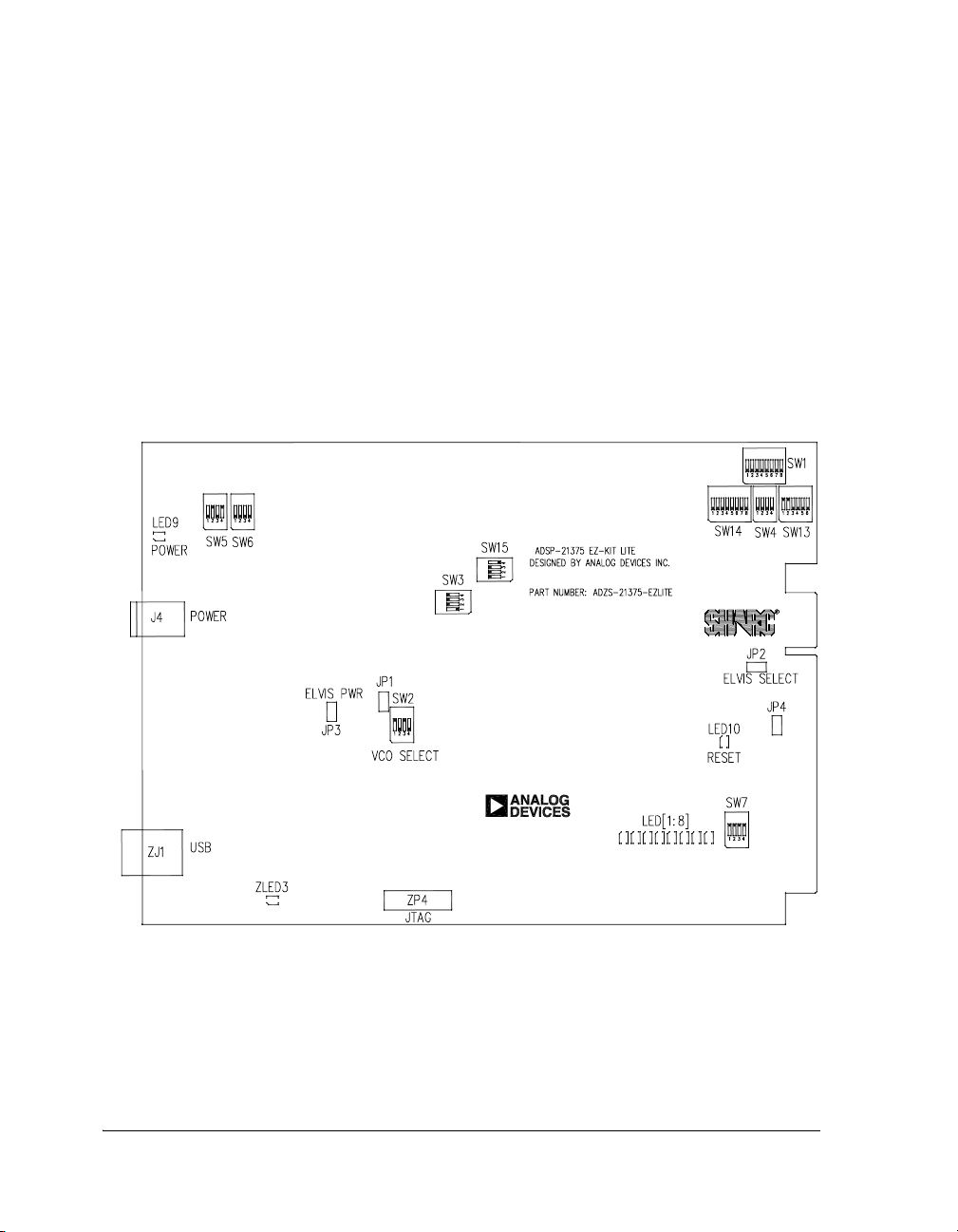
2. Figure 1-1 shows the default jumper settings, DIP switch, connector locations, and LEDs used in installation. Confirm that your
board is set up in the default configuration before continuing.
Figure 1-1. EZ-KIT Lite Hardware Setup
1-4 ADSP-21375 EZ-KIT Lite Evaluation System Manual
Page 27

Using ADSP-21375 EZ-KIT Lite
3. Plug the provided power supply into
Visually verify that the green power LED (LED9) is on. Also verify
that the red reset LED (LED10) goes on for a moment and then goes
off, and, finally, LED1 through LED8 are sequentially blinking.
4. Connect one end of the USB cable to an available full speed USB
port on your PC and the other end to ZJ1 on the ADSP-21375
EZ-KIT Lite board.
J4 on the EZ-KIT Lite board.
Installation and Session Startup
L
For correct operation, install the software and hardware in the
order presented in the VisualDSP++ Installation Quick Reference
Card.
1. Verify that the yellow USB monitor LED (ZLED3, located near the
USB connector) is lit. This signifies that the board is communicating properly with the host PC and is ready to run VisualDSP++.
2. If you are running VisualDSP++ for the first time, navigate to the
VisualDSP++ environment via the Start –> Programs menu. The
main window appears. Note that VisualDSP++ does not connect to
any session. Skip the rest of this step to step 3.
If you have run VisualDSP++ previously, the last opened session
appears on the screen. You can override the default behavior and
force VisualDSP++ to start a new session by pressing and holding
down the Ctrl key while starting VisualDSP++. Do not release the
Ctrl key until the Session Wizard appears on the screen. Go to
step 4.
ADSP-21375 EZ-KIT Lite Evaluation System Manual 1-5
Page 28

Installation and Session Startup
3. To connect to a new EZ-KIT Lite session, start Session Wizard by
selecting one of the following.
• From the Session menu, New Session.
• From the Session menu, Session List. Then click New Ses-
sion from the Session List dialog box.
• From the Session menu, Connect to Target.
4. The Select Processor page of the wizard appears on the screen.
Ensure SHARC is selected in Processor family. In Choose a target
processor, select ADSP-21375. Click Next.
5. The Select Connection Type page of the wizard appears on the
screen. Select EZ-KIT Lite and click Next.
6. The Select Platform page of the wizard appears on the screen.
Ensure that the selected platform is ADSP-21375 EZ-KIT Lite via
Debug Agent. Specify your own Session name for your session or
accept the default name.
The session name can be a string of any length; although, the box
displays approximately 32 characters. The session name can
include space characters. If you do not specify a session name,
VisualDSP++ creates a session name by combining the name of the
selected platform with the selected processor. The only way to
change a session name later is to delete the session and to open a
new session.
Click Next.
7. The Finish page of the wizard appears on the screen. The page dis-
plays your selections.Check the selections. If you are not satisfied,
click Back to make changes; otherwise, click Finish. VisualDSP++
1-6 ADSP-21375 EZ-KIT Lite Evaluation System Manual
Page 29

Using ADSP-21375 EZ-KIT Lite
creates the new session and connects to the EZ-KIT Lite. Once
connected, the main window’s title is changed to include the session name set in step 6
L
To disconnect from a session, click the disconnect button
or select Session–>Disconnect from Target.
To delete a session, select Session –> Session List. Select the ses-
sion name from the list and click Delete. Click OK.
Evaluation License Restrictions
The ADSP-21375 EZ-KIT Lite installation is part of the VisualDSP++
installation. The EZ-KIT Lite is a licensed product that offers an unrestricted evaluation license for the first 90 days. Once the initial
unrestricted 90-day evaluation license expires:
1. VisualDSP++ allows a connection to the ADSP-21375 EZ-KIT
Lite via the USB Debug Agent interface only. Connections to simulators and emulation products are no longer allowed.
2. The linker restricts a user’s program to 10922 words of internal
memory for code space with no restrictions for data space.
Refer to the VisualDSP++ Installation Quick Reference Card for details.
External Memory
The EZ-KIT Lite contains three types of memory: parallel flash (1 MB),
SPI flash (2 Mbit), and SDRAM (128 Mbit). The flash memories can
store user-specific boot code, allowing the board to run as a stand-alone
unit. For more information about selecting the boot device for the processor, see “Boot Mode and Clock Ratio Select Switch (SW2)” on page 2-10.
ADSP-21375 EZ-KIT Lite Evaluation System Manual 1-7
Page 30

External Memory
Table 1-1 provides start and end addresses of the board’s external
memories.
Table 1-1. EZ-KIT Lite Evaluation Board External Memory
Start Address End Address Content
0x0020 0000 0x011F 0000 SDRAM memory (~MS0)
0x0400 0000 0x040F FFFF Flash memory (~MS1)
0x0800 0000
0x0800 0000
0x0C00 0000
0x0C00 0000
0x08FF FFFF
0x0BFF FFFF
0x0CFF FFFF
0x0FFF FFFF
Unused chip select (~MS2) for non-SDRAM addresses
Unused chip select (
Unused chip select (~MS3) for non-SDRAM addresses
Unused chip select (~MS3) for SDRAM addresses
~MS2) for SDRAM address
The parallel flash memory and SDRAM connect to the external memory
of the processor.
The SDRAM memory connects to the SDRAM controller of the processor. A set of programmable timing parameters is available to configure the
SDRAM banks to support slower memory accesses. Care must be taken
when configuring the SDRAM control registers. For more information
regarding the setup of the SDRAM controller, please refer to the
ADSP-21368 SHARC Processor Hardware Reference (includes
ADSP-21375). An example program is included in the EZ-KIT Lite
installation directory to demonstrate the SDRAM setup.
The SPI flash memory connects to the SPI port of the processor and
designates:
•DPI pin5 (DPI5) as a chip select
•DPI pin3 (
•DPI pin1 (
DPI3) as the SPI clock
DPI1) as the MOSI
•DPI pin2 (DPI2) as the MISO
1-8 ADSP-21375 EZ-KIT Lite Evaluation System Manual
Page 31

Using ADSP-21375 EZ-KIT Lite
By default, the DPI is set up for the SPI flash, and any required changes to
the SPI flash can be made by modifying the DPI of the processor. An
example program is included in the EZ-KIT Lite installation directory to
demonstrate the SPI flash memory reads and writes.
The parallel flash memory connects to the asynchronous memory controller of the processor. Each of their respective memory banks can be
independently programmed with different timing parameters. For more
information on changing wait states to speed up or slow down the asynchronous controller and other setup information, refer to the
ADSP-21368 SHARC Processor Hardware Reference (includes
ADSP-21375). Example programs are included in the EZ-KIT Lite installation directory to demonstrate the flash memory reads and writes.
ELVIS Interface
The ADSP-21375 EZ-KIT Lite board contains the National Instruments
Educational Laboratory Virtual Instrumentation Suite interface. The
interface features the DC voltage and current measurement modules,
oscilloscope and bode analyzer modules, function generator, arbitrary
waveform generator, and digital IO.
The ELVIS interface is a LabVIEW-based design and prototype environment for university science and engineering laboratories. The ELVIS
interface consists of LabVIEW-based virtual instruments, a multifunction
data acquisition (DAQ) device, and a custom-designed bench-top workstation and prototype board. This combination provides a ready-to-use
suite of instruments found in most educational laboratories. Because the
interface is based on LabVIEW and provides complete data acquisition
and prototyping capabilities, the system is ideal for academic coursework
that range from lower-division classes to advanced project-based
curriculums.
For more information on ELVIS and example demonstration programs,
visit National Instruments Web site at
ADSP-21375 EZ-KIT Lite Evaluation System Manual 1-9
www.ni.com.
Page 32

Analog Audio
Analog Audio
The AD1835A is a high-performance, single-chip codec featuring four stereo digital-to-analog converters (DACs) for audio output and one stereo
analog-to-digital converters (ADCs) for audio input. The codec can input
and output data with a sample rate of up to 96 kHz on all channels. A
192 kHz sample rate can be used with one of the DAC channels.
The processor is interfaced with the AD1835A via the DAI port. The DAI
interface pins can be configured to transfer serial data from the AD1835A
codec in either time-division multiplexed (TDM) or two-wire interface
mode (TWI). For more information on the AD1835A connection to the
DAI, see “DAI Interface” on page 2-4.
The master input clock (MCLK) for the AD1835A device can be generated
by the on-board 12.288 MHz oscillator or can be supplied by one of the
DAI pins of the processor. Using one of the pins to generate the MCLK, as
opposed to the on-board oscillator, allows synchronization of multiple
devices in the system. It is possible to disable the on-board audio oscillator
from driving the audio codec and the processor’s input pin. For instructions on how to configure the clock, refer to “Codec Setup Switch (SW3)”
on page 2-11.
The AD1835A codec can be configured as a master or as a slave, depending on the DIP switch settings. In master mode, the AD1835A drives the
serial port clock and frame sync signals to the processor. In slave mode,
the processor must generate and drive all of the serial port clock and frame
sync signals. For information on how to set up the mode, refer to “Codec
Setup Switch (SW3)” on page 2-11.
The internal configuration registers of the AD1835A codec are configured
using the SPI port of the processor. The DPI pin 4 (DPI4 register) is used
as the select for the device. For information on how to configure the multichannel codec, refer to the product datasheet at
http://www.analog.com/en/prod/0,2877,AD1835A,00.html.
1-10 ADSP-21375 EZ-KIT Lite Evaluation System Manual
Page 33

Using ADSP-21375 EZ-KIT Lite
The RCA connector (
electret microphone on this connector, configure the SW4 switch according
to the instructions in “Electret Microphone Select Switch (SW4)” on
page 2-12. The four output channels connect to the RCA connector J5.
Channel 4 of the codec connects to the headphone jack J9. For more
information about the connectors see “Connectors” on page 2-21.
Example programs are included in the EZ-KIT Lite installation directory
to demonstrate how to configure and use the board’s analog audio
interface.
J10) is used to input analog audio. When using an
LEDs and Push Buttons
The EZ-KIT Lite has eight general-purpose user LEDs and four general-purpose push buttons.
Two of the general-purpose push buttons are attached to the FLAG pins of
the processor, while the other two are attached to the DAI pins. All of the
push buttons connect to the processor through a DIP switch. The DIP
switch allows processor pins, which connect to the push buttons, to be disconnected. See “Push Button Enable Switch (SW7)” on page 2-13 for
instructions on how to disable a push button from driving its corresponding processor pin.
The state of the push buttons, connected to the
mined by reading the FLAG register. The push buttons connected to the
DAI pins must be configured as interrupts. It is necessary to set up an
interrupt routine to determine each pin’s state. Table 1-2 shows the push
button and processor connections. Refer to the related example program
shipped with the EZ-KIT Lite for more information.
ADSP-21375 EZ-KIT Lite Evaluation System Manual 1-11
FLAG pins, can be deter-
Page 34

LEDs and Push Buttons
Table 1-2. Push Button Connections
Push Button Label Push Button Reference Designator Processor Pin
PB1 SW8 FLAG1/~IRQ1
PB2 SW11 FLAG0/~IRQ0
PB3 SW10 DAI19
PB4 SW9 DAI20
Table 1-3 summarizes the LED connections to the processor. To use the
LEDs connected to the DAI or DPI, configure the respective registers of
the processor. For more information, refer to the ADSP-21368 SHARC
Processor Hardware Reference (includes ADSP-21375).
Table 1-3. LED Connections
LED Reference Designator Processor Pin
LED1 DPI6
LED2 DPI7
LED3 DPI8
LED4 DPI13
LED5 DPI14
LED6 DAI15
LED7 DAI16
LED8 FLAG3/~MS3/~IRQ3
An example program is included in the EZ-KIT Lite installation
L
directory to demonstrate the functionality of the LEDs and push
buttons.
1-12 ADSP-21375 EZ-KIT Lite Evaluation System Manual
Page 35

Using ADSP-21375 EZ-KIT Lite
Example Programs
Example programs are provided with the ADSP-21375 EZ-KIT Lite to
demonstrate various capabilities of the evaluation board. These programs
are installed with the EZ-KIT Lite software in the
…\213xx\Examples\ADSP-21375 EZ-KIT Lite subdirectory of the Visu-
alDSP++ installation directory. Please refer to the readme file provided
with each example for more information.
Background Telemetry Channel
The ADSP-21375 USB debug agent supports the background telemetry
channel (BTC), which facilitates data exchange between VisualDSP++ and
the processor without interrupting processor execution.
The BTC allows you to view a variable as it is updated or changed, all
while the processor continues to execute. For increased performance of the
BTC, including faster reading and writing, please check our latest line of
SHARC processor emulators at http://www.analog.com/proces-
sors/sharc/evaluationDevelopment/crosscore/index.html. For more
information about the background telemetry channel, see the VisualDSP++ User’s Guide or online Help.
ADSP-21375 EZ-KIT Lite Evaluation System Manual 1-13
Page 36

Background Telemetry Channel
1-14 ADSP-21375 EZ-KIT Lite Evaluation System Manual
Page 37

2 ADSP-21375 EZ-KIT LITE
HARDWARE REFERENCE
This chapter describes the hardware design of the ADSP-21375 EZ-KIT
Lite board. The following topics are covered.
• “System Architecture” on page 2-2
Describes the configuration of the ADSP-21375 board and
explains how the board components interface with the processor.
• “Switch Settings” on page 2-9
Shows the location and describes the function of the board
switches.
• “LEDs and Push Buttons” on page 2-15
Shows the location and describes the function of the board LEDs
and push buttons.
• “Jumpers” on page 2-18
Shows the location and describes the function of the board
jumpers.
• “Connectors” on page 2-21
Shows the location and gives the part number for all of the connectors on the board. Also, the manufacturer and part number
information is given for the mating parts.
ADSP-21375 EZ-KIT Lite Evaluation System Manual 2-1
Page 38

System Architecture
System Architecture
This section describes the processor’s configuration on the EZ-KIT Lite
board (Figure 2-1).
DPI
Conn
RS
232
Conn
+7.0V
USB Connector
Connector
SRAM
EZ USB FX
16.384 MHz
Oscillator
Reset PB
ADM3202
A5V
3.3V
1.2V
Power Regulation
JTAG
Header
LEDs
(5)
4
JTAG Port
ADSP-21375
DPI
SPI FLASH
FLAGs
0,1, and 3
2 2
PBs (4)
DSP
8M x 16
SDRAM
Stereo In RCA
Jacks (2x1)
Parallel
Port
DAI
AD1835
CODEC
Stereo Out RCA
Jacks (4x2)
1M x 8
Flash
Expansion
Connectors
Headphone
Jack
Type A
Conn
ELVIS
Conn
DAI
Figure 2-1. System Architecture Block Diagram
This EZ-KIT Lite has been designed to demonstrate the capabilities of the
ADSP-21375 processor. The processor core is powered at 1.2V, and the
IO is powered at 3.3V.
2-2 ADSP-21375 EZ-KIT Lite Evaluation System Manual
Page 39

ADSP-21375 EZ-KIT Lite Hardware Reference
The
CLKIN pin of the processor connects to a 16.384 MHz oscillator. The
core frequency of the processor is derived by multiplying the frequency at
the CLKIN pin by a value determined by the state of the processor pins
CLKCFG1 and CLKCFG0. The value at these pins is determined by the state of
the SW2 switch (see “Boot Mode and Clock Ratio Select Switch (SW2)” on
page 2-10). By default, the EZ-KIT Lite gives a core frequency of
262.144 MHz. It is possible to change the speed of the processor by
changing the value of the PMCTL register.
The SW2 switch also configures the boot mode of the processor. The
EZ-KIT Lite is capable of EPROM/flash boot and SPI boot. By default,
the EZ-KIT Lite boots from the flash memory. For information about
configuring the boot modes, see “Boot Mode and Clock Ratio Select
Switch (SW2)” on page 2-10.
External Port
The external port of the ADSP-21375 processor consists of a 24-bit
address bus, 16-bit data memory bus, and control lines. The control lines
are used to select, read, and write to external memory devices.
The external port connects to an 8-bit parallel flash memory and a 16-bit
SDRAM memory. See “External Memory” on page 1-7 for more information about accessing the flash and SDRAM memories.
All of the external port signals are available externally via the expansion
interface connectors (J1–3). The pinout of the connectors can be found in
“ADSP-21375 EZ-KIT Lite Schematic” on page B-1.
ADSP-21375 EZ-KIT Lite Evaluation System Manual 2-3
Page 40

System Architecture
DAI Interface
The digital application interface (DAI) pins connect to the signal routing
unit (SRU) of the processor. The SRU is a flexible routing system, providing a large system of signal flows within the processor. In general, the SRU
allows to route the DAI pins to different internal peripherals in various
combinations.
The DAI pins connect to the AD1835A audio codec, a 26-pin header, two
RCA connectors, audio oscillator output, an external phase lock loop
(PLL) circuit, two LEDs, and two push buttons. Figure 2-2 illustrates the
EZ-KIT Lite’s connections to the DAI.
DAI20 (SFS45)
DAI19 (SCLK45)
DAI18 (SD5B)
DAI17 (SD5A)
DAI16 (SD4B)
DAI15 (SD4A)
DAI14 (SFS23)
DAI13 (SCLK23)
DAI12 (SD3B)
DAI11 (SD3A)
DAI10 (SD2B)
DAI9 (SD2A)
DAI8 (SFS1)
DAI7 (SCLK1)
DAI5 (SD1A)
DAI6 (SD1B)
DAI4 (SFS0)
DAI3 (SCLK0)
DAI2 (SD0B)
DAI1 (SD0A)
DSP
PB_4
PB_3
SPDIF IN
AUDIO OSC
LED7
LED6
ELVIS_TRIG
PLLMCLK IN
PLLMCLK OUT
SPDIF OUT
DAC_LRCLK
DAC_BCLK
DAC_SDATA1
DAC_SDATA2
DAC_SDATA3
DAC_SDATA4
ADC_LRCLK
ADC_BCLK
ADC_SDATA1
MCLK
12.288MHz
Figure 2-2. DAI Connections Block Diagram
AD1835
DAC1
DAC2
DAC3
DAC4
ADC
4x2
RCA
Phono
Jack
OUT
Headphone
Jack
1X2
RCA
Phono
Jack IN
2-4 ADSP-21375 EZ-KIT Lite Evaluation System Manual
Page 41

ADSP-21375 EZ-KIT Lite Hardware Reference
To use the DAI for a different purpose, disable any signal driving the DAI
pin with a switch (see “Codec Setup Switch (SW3)” on page 2-11). In
addition, the
SW3 switch allows flexible routing of the 12.288 MHz audio
oscillator’s output signal. By default, this signal is used as the master clock
(MCLK) for the AD1835A codec.
All of the DAI signals are available externally via the expansion interface
connectors (J1–3), as well as the 0.1” spaced header P4. The pinout of the
connectors can be found in “ADSP-21375 EZ-KIT Lite Schematic” on
page B-1.
DPI Interface
The digital peripheral interface (DPI) pins connect to a second signal
routing unit of the processor (SRU2). The SRU2 unit, similar to the SRU, is a
flexible routing system, providing a large system of signal flows within the
processor. In general, the SRU2 allows to route the DPI pins to different
internal peripherals in various combinations.
ADSP-21375
DPI12 (UART CTS)
DPI11 (UART RTS)
DPI10 (UART RX)
DPI9 (UART TX)
DPI14 (LED5)
DPI13 (LED4)
DPI8 (LED3)
DPI7 (LED2)
DPI6 (LED1)
DPI5 (SPI_FLASHCS)
DPI4 (SPI_AD1835CS)
DPI3 (SPICLK)
DPI2 (MISO)
DPI1 (MOSI)
LED5
LED4
LED3
LED2
LED1
T2IN
R2OUT
R1OUT
T1IN
CS/
SCK
SO
SI
CLATCH
CCLK
COUT
CIN
ADM3202
SPI
FLASH
AD1835
T2OUT
R2IN
R1IN
T1OUT
DB-9
Conn
Figure 2-3. DPI Connections Block Diagram
ADSP-21375 EZ-KIT Lite Evaluation System Manual 2-5
Page 42

System Architecture
The DPI pins connect to the SPI flash memory, the SPI interface of the
AD1835A codec, a UART, a 20-pin header, and five LEDs. Figure 2-3
illustrates the EZ-KIT Lite’s connections to the DPI.
To use the DPI for a different purpose, disable any signal driving the DPI
pins with a switch (see “UART Enable Switch (SW5)” on page 2-12). Any
DPI pin connected to a LED can be used without having to disconnect
the pin. You can, however, see the respective LED turn
ON and OFF when
using the signal elsewhere on the board.
All of the DPI signals are available externally via the expansion interface
connectors (J1–3), as well as the 0.1” spaced header P3. The pinout of
these connectors can be found in “ADSP-21375 EZ-KIT Lite Schematic”
on page B-1.
FLAG Pins
The processor has four general-purpose IO flag pins. Table 2-1 describes
the flag connections.
Table 2-1. IO FLAG Pins
FLAG Pin EZ-KIT Lite Function
FLAG0 Push button (SW2) input
FLAG1 Push button (SW2) input
FLAG2 SDRAM chip select
FLAG3 LED8
For information on how to disable a push button from driving its corresponding processor flag pin, see “Push Button Enable Switch (SW7)” on
page 2-13.
2-6 ADSP-21375 EZ-KIT Lite Evaluation System Manual
Page 43

ADSP-21375 EZ-KIT Lite Hardware Reference
The
FLAG signals are available externally via the expansion interface con-
nectors (J1–3). The pinout of these connectors can be found in
“ADSP-21375 EZ-KIT Lite Schematic” on page B-1.
External PLL
The ADSP-21375 EZ-KIT Lite contains an external phase lock loop to
help generate a faster and more stable master input clock
MCLK. The PLL
uses DAI pin 3 as an input clock from the ADSP-21375 processor. The
new clock generated by PLL connects to the processor via DAI pin 2.
Example programs are included in the EZ-KIT Lite installation directory
to demonstrate how to configure and use the board’s external PLL.
Expansion Interface
The expansion interface consists of the three 90-pin connectors. Table 2-2
shows the interfaces each connector provides. For the exact pinout of the
connectors, refer to “ADSP-21375 EZ-KIT Lite Schematic” on page B-1.
The mechanical dimensions of the connectors can be obtained from Tech-
nical or Customer Support.
Table 2-2. Expansion Interface Connectors
Connector Interfaces
J1 5V, ADDR23–0, DATA31–0
J2 3.3V, FLAG3–0, DAIP20–1, DPI14–1, SDRAM control signals
J3 5V, 3.3V, reset, parallel port control signals
ADSP-21375 EZ-KIT Lite Evaluation System Manual 2-7
Page 44

System Architecture
Limits to the current and to the interface speed must be taken into consideration when using the expansion interface. The maximum current limit is
dependent on the capabilities of the used regulator. Additional circuitry
also can add extra loading to signals, decreasing their maximum effective
speed.
[
Analog Devices does not support and is not responsible for the
effects of additional circuitry.
JTAG Emulation Port
The JTAG emulation port allows an emulator to access the internal and
external memory of the processor through a 6-pin interface. The JTAG
emulation port of the processor also connects to the USB debugging interface. When an emulator connects to the board at ZP4, the USB debugging
interface is disabled. This is not a standard connection of the JTAG
interface.
For information about the standard connection of the interface, see EE-68
published on the Analog Devices Web site. For more information about
the JTAG connector, see “JTAG Header (ZP4)” on page 2-25. To learn
more about available SHARC processor emulators, go to
http://www.analog.com/processors/sharc/evaluationDevelopment/crosscore/index.html
.
2-8 ADSP-21375 EZ-KIT Lite Evaluation System Manual
Page 45

ADSP-21375 EZ-KIT Lite Hardware Reference
Switch Settings
This section describes the function of the EZ-KIT Lite switches.
Figure 2-4 shows the switch locations and default settings.
Figure 2-4. Switch Locations and Default Settings
ADSP-21375 EZ-KIT Lite Evaluation System Manual 2-9
Page 46

Switch Settings
Boot Mode and Clock Ratio Select Switch (SW2)
The SW2 switch sets the boot mode and clock multiplier ratio. Table 2-3
shows how to set up the boot mode using SW2 positions 1 and 2. By
default, the EZ-KIT Lite boots in external port mode from the flash
memory.
Table 2-3. Boot Mode Configuration Switch (SW2)
BOOTCFG0 Pin (Position 1) BOOTCFG1 Pin (Position 2) Boot Mode
ON ON SPI slave boot
ON OFF Parallel flash boot (default)
OFF ON SPI master boot
OFF
OFF Reserved
Table 2-4 shows how to set up the clock multiply ratio using SW2
positions 3 and 4. By default, the processor increases the clock multiply
ratio by sixteen, setting the core clock to 262.144 MHz.
Table 2-4. Core Clock Rate Configuration
CLKCFG0 (Position 3) CLKCFG1 (Position 4) Core to CLKIN Ratio
ON ON 6:1
ON OFF 16:1 (default)
OFF ON 32:1
OFF
OFF Reserved
The core clock frequency can be increased or decreased via software by
writing to the PMCTL register. For more information on changing the core
clock frequency and other setup information, refer to the ADSP-21368
SHARC Processor Hardware Reference (includes ADSP-21375).
2-10 ADSP-21375 EZ-KIT Lite Evaluation System Manual
Page 47

ADSP-21375 EZ-KIT Lite Hardware Reference
Codec Setup Switch (SW3)
The codec setup switch (SW3) can be used to change the routing of some
signals going to the AD1835A codec and to set up the communication
protocol of the codec.
SW3 positions 1 and 2 determine the clock routing for the audio oscillator
to the codec and to the processor. Figure 2-5 illustrates how the switch
positions 1 and 2 connect on the board. In the default position, route the
DAI_P17 pin to DAI_P6 (in software) to clock the AD1835A codec.
ADSP-21375 Processor AD1835A Codec
DAI_P6
DAI_P17
SW3.1
SW3.2
MCLK
12.288 MHz
OSC
Figure 2-5. Audio Clock Routing
SW3 position 3 determines if the AD1835A device is a master or a slave. If
the AD1835A is a master, the device’s serial interface generates the frame
sync and clock signals necessary to transfer data. When the device is a
slave, the processor must generate the frame sync and clock signals. By
default, position 3 is ON, and the AD1835A codec generates the control
signals.
SW3 position 4 disconnects the AD1835A codec’s ADC_DATA pin from the
DAI interface. This is useful when the DAI interface connects to another
device.
ADSP-21375 EZ-KIT Lite Evaluation System Manual 2-11
Page 48

Switch Settings
Electret Microphone Select Switch (SW4)
To connect an electret microphone to the audio input, place all positions
of the SW4 switch ON. The default position of the switch is all OFF. When all
of the SW4 positions are ON, a DC offset of 2.5V is added to the signal, and
gain of the input amplifiers is changed from 1x to 10x.
UART Enable Switch (SW5)
The UART enable switch (SW5) disconnects UART signals from the DPI
pins of the processor. When the switch is OFF, the associated DPI signal
(see Table 2-5) can be used on the expansion interface.
Table 2-5. UART Enable Switch (SW5)
Switch Position EZ-KIT Lite Signal Processor Signal
1 (OFF
1
)
CTS DPI12
2 (ON) RX DPI10
3 (OFF) RTS DPI11
4 (ON) T2IN tied to R2OUT N/A
1 Bold typeface denotes the default setting.
Loop-Back Test Switches (SW6 and SW14)
The loop-back test switch SW6 is located at the top left side of the board.
The second loop-back test switch,
the board. These switches are used only for testing; all switch positions
should remain
OFF.
2-12 ADSP-21375 EZ-KIT Lite Evaluation System Manual
SW14, is located at the top right side of
Page 49

ADSP-21375 EZ-KIT Lite Hardware Reference
Push Button Enable Switch (SW7)
The push button enable switch (SW7) disconnects the push buttons from
the corresponding processor pins. This allows the signals to be used elsewhere on the board. Table 2-6 shows the SW7 connections. By default, all
position of the SW7 switch are ON, allowing the push buttons to function as
designed.
Table 2-6. Push Button Enable Switch (SW7)
Switch Position Push Button Label Push Button Reference Designator Processor Pin
1
2 PB2 SW11 FLAG0/~IRQ0
3 PB3 SW10 DAI19
4 PB4 SW9 DAI20
PB1 SW8 FLAG1/~IRQ
ELVIS Oscilloscope Configuration Switch (SW1)
The oscilloscope configuration switch (SW1) determines which audio circuit signals connect to channels A and B of the oscilloscope. The switch is
used only when the board connects to the Educational Laboratory Virtual
Instrumentation Suite (ELVIS) station (see “ELVIS Interface” on
page 1-9). Each channel must have only one signal selected at a time, as
described in Table 2-7.
Table 2-7. Oscilloscope Configuration Switch (SW1)
Channel Switch Position Audio Circuit Signal
A
A2 (OFF) AMP_RIGHT_IN
A3 (OFF) LEFT_OUT
1 (OFF
1
)
AMP_LEFT_IN
A4 (OFF) RIGHT_OUT
B5 (OFF) AMP_LEFT_IN
ADSP-21375 EZ-KIT Lite Evaluation System Manual 2-13
Page 50

Switch Settings
Table 2-7. Oscilloscope Configuration Switch (SW1) (Cont’d)
Channel Switch Position Audio Circuit Signal
B6 (OFF) AMP_RIGHT_IN
B7 (OFF) LEFT_OUT
B8 (OFF) RIGHT_OUT
1 Bold typeface denotes the default settings.
ELVIS Function Generator Configuration Switch (SW13)
The function generator configuration switch (SW13) controls which signals
connect to the left and right input signals of the audio interface. The SW13
switch is used only when the board connects to the ELVIS station (see
“ELVIS Interface” on page 1-9). Each channel must have only one signal
selected at a time, as described in Table 2-8.
Table 2-8. ELVIS Function Generator Configuration Switch (SW13)
Channel Switch Position Audio Signal
AMP_LEFT_IN
AMP_RIGHT_IN 2 (ON) RIGHT_IN
AMP_LEFT_IN
AMP_RIGHT_IN 4 (OFF) DAC1
AMP_LEFT_IN 5 (OFF) FUNCT_OUT
AMP_RIGHT_IN 6 (OFF) FUNCT_OUT
1 Bold typeface denotes the default settings.
1 (ON1)
3 (OFF) DAC0
LEFT_IN
2-14 ADSP-21375 EZ-KIT Lite Evaluation System Manual
Page 51

ADSP-21375 EZ-KIT Lite Hardware Reference
AD1835A and Flash Disconnect Switch (SW15)
The AD1835A and flash disconnect switch (SW15) disconnects the following signals: DPI4_SPI_AD1835_CS, DAIP8_ADC_LRCLK, and
DPI5_SPI_FLASH_CS. The switch is used only for expansion interface pur-
poses; by default, the switch positions 1–3 are ON and position 4 is OFF.
LEDs and Push Buttons
This section describes the functionality of the LEDs and push buttons.
Figure 2-6 shows the LED and push button locations.
Figure 2-6. LED and Push Button Locations
ADSP-21375 EZ-KIT Lite Evaluation System Manual 2-15
Page 52

LEDs and Push Buttons
General Purpose LEDs (LED1–8)
There are eight general-purpose LEDs on the board. Five LEDs connect to
the DPI interface, two LEDs connect to the DAI interface, and one LED
connects to FLAG3 of the processor. “LEDs and Push Buttons” on
page 1-11 summarizes the LED connections. The respective registers of
the processor must be programmed appropriately in order to use LEDs
connected to the DAI or DPI. For more information on how to program
the registers, refer to the ADSP-21368 SHARC Processor Hardware Refer-
ence (includes ADSP-21375).
Power LED (LED9)
When LED9 is lit (green), it indicates that power is being supplied to the
board properly.
Reset LED (LED10)
When LED10 is lit (red), the master reset of all the major ICs is active.
USB Monitor LED (ZLED3)
The USB monitor LED (ZLED3) indicates that USB communication has
been initialized successfully, and you can connect to the processor using a
VisualDSP++ EZ-KIT Lite session. Once the USB cable is plugged into
the board, it takes approximately 15 seconds for the USB monitor LED to
light. If the LED does not light, try cycling power on the board and/or
reinstalling the USB driver (see the VisualDSP++ Installation Quick Refer-
ence Card).
L
2-16 ADSP-21375 EZ-KIT Lite Evaluation System Manual
When VisualDSP++ is actively communicating with the EZ-KIT
Lite target board, the LED can flicker, indicating communications
handshake.
Page 53

ADSP-21375 EZ-KIT Lite Hardware Reference
Push Buttons (SW8–11)
Four push buttons (SW8–11) are provided for general-purpose user input:
two push buttons connect to the FLAG pins of the processor, while the
other two connect to the DAI of the processor. The push buttons are
active high and, when pressed, send a high (1) to the processor. Refer to
“LEDs and Push Buttons” on page 1-11 for more information. The push
button enable switch (SW7) is capable of disconnecting the push buttons
from the corresponding processor pins (refer to “Push Button Enable
Switch (SW7)” on page 2-13 for more information).
The push buttons and corresponding processor signals are summarized in
Table 2-9.
Table 2-9. Push Button Connections
Push Button Label Push Button Reference Designator Processor Pin
PB1 SW8 FLAG1/~IRQ1
PB2 SW11 FLAG0/~IRQ0
PB3 SW10 DAI19
PB4 SW9 DAI20
Board Reset Push Button (SW12)
The RESET push button (SW12) resets all of the ICs on the board. The only
exception is the USB interface chips. These chips are not being reset when
the push button is pressed after the USB cable has been plugged in and
communication correctly initialized with the PC. After USB communication has been initialized, the only way to reset the USB is by powering
down the board.
ADSP-21375 EZ-KIT Lite Evaluation System Manual 2-17
Page 54

Jumpers
Jumpers
Figure 2-7 shows the locations and default settings of the EZ-KIT Lite
jumpers.
Figure 2-7. Jumper Locations
2-18 ADSP-21375 EZ-KIT Lite Evaluation System Manual
Page 55

ADSP-21375 EZ-KIT Lite Hardware Reference
VCO Select Jumper (JP1)
The voltage-controlled oscillator (VCO) select jumper (JP1) configures
the frequency selection of the on-board external PLL (U39). When JP1 is
installed, the VCO output frequency is multiplied by a factor of 1.0. Conversely, when uninstalled, the VCO output frequency is multiplied by a
factor of 0.5 or divided in half. The jumper settings are shown in
Table 2-10.
Table 2-10. VCO Select Jumper (JP1)
JP1 Setting Mode
OFF VCO output frequency x ½ (default)
ON VCO output frequency x 1.0
ELVIS Select Jumper (JP2)
The ELVIS select jumper (JP2) configures the EZ-KIT Lite’s connection
to an ELVIS station (see “ELVIS Interface” on page 1-9). When JP2 is
installed, the connections to the push buttons and LED are re-directed to
the ELVIS station instead of the processor. The jumper settings are shown
in Table 2-11.
Table 2-11. ELVIS Select Jumper (JP2)
JP2 Setting Mode
OFF Not connected to an ELVIS station (default)
ON Connected to an ELVIS station
ADSP-21375 EZ-KIT Lite Evaluation System Manual 2-19
Page 56

Jumpers
ELVIS Voltage Selection Jumper (JP3)
The ELVIS voltage selection jumper (JP3) is used to select the power
source for the EZ-KIT Lite. In a standard mode of operation, the board
receives its power from an external power supply. When JP3 is installed,
the board is powered from an ELVIS station and no external power supply
is required. The jumper settings are shown in Table 2-12.
Table 2-12. ELVIS Voltage Selection Jumper (JP3)
JP3 Setting Mode
OFF Powered from an external power supply (default)
ON Powered from an ELVIS station
[
when JP3 is installed to avoid potential damage to the EZ-KIT Lite
board and ELVIS unit.
ELVIS Programmable Flag Jumper (JP4)
The ELVIS programmable flag jumper (JP4) connects the ADSP-21375
processor’s DAI4 pin to the ELVIS trigger pin. When JP4 is installed, DAI4
connects to the ELVIS TRIG1_2 pin directly. Conversely, when JP4 is
The external power supply must be disconnected from the board
uninstalled, the
non-ELVIS operation. The jumper settings are shown in Table 2-13.
Table 2-13. ELVIS Select Jumper (JP4)
JP4 Setting Mode
OFF DAI4 disconnected from the ELVIS TRIG pin (default)
ON DAI4 connected to the ELVIS TRIG pin
DAIP4 pin is disconnected and can be used for another
2-20 ADSP-21375 EZ-KIT Lite Evaluation System Manual
Page 57

ADSP-21375 EZ-KIT Lite Hardware Reference
Connectors
This section describes the connector functionality and provides information about mating connectors. Figure 2-8 shows the connector locations.
Figure 2-8. Connector Locations
ADSP-21375 EZ-KIT Lite Evaluation System Manual 2-21
Page 58

Connectors
Expansion Interface Connectors (J1–3)
Three board-to-board connectors (J1–3) provide signals for most of the
processor’s peripheral interfaces. The connectors are located at the bottom
of the board. For more information about the expansion interface, see
“Expansion Interface” on page 2-7. For the J1–3 connectors’ availability
and pricing, contact Samtec.
Part Description Manufacturer Part Number
90-position 0.05” spacing, SMT SAMTEC SFC-145-T2-F-D-A
Mating Connectors
90-position 0.05” spacing
(through hole)
90-position 0.05” spacing
(surface mount)
90-position 0.05” spacing
(low cost)
SAMTEC TFM-145-x1 series
SAMTEC TFM-145-x2 series
SAMTEC TFC-145 series
Audio In RCA Connector (J10)
Part Description Manufacturer Part Number
Two-channel right angle RCA jack SWITCHCRAFT PJRAS1X2S02
Mating Cable
Two-channel RCA interconnect cable MONSTER CABLE BI100-1M
Audio Out RCA Connector (J5)
Part Description Manufacturer Part Number
Four-channel right angle RCA jack SWITCHCRAFT PJRAS4X2U01
2-22 ADSP-21375 EZ-KIT Lite Evaluation System Manual
Page 59

ADSP-21375 EZ-KIT Lite Hardware Reference
Part Description Manufacturer Part Number
Mating Cable
Two-channel RCA interconnect cable MONSTER CABLE BI100-1M
Headphone Out Jack (J9)
Part Description Manufacturer Part Number
3.5 mm stereo jack A/D ELECTRONICS ST-323-5
Power Jack (J4)
The power connector (J4) provides all of the power necessary to operate
the EZ-KIT Lite board.
Part Description Manufacturer Part Number
2.5 mm power jack SWITCHCRAFT
DIGI-KEY
Mating Power Supply (shipped with EZ-KIT Lite)
7V power supply CUI INC. DMS070214-P6P-SZ
RAPC712X-ND
The power connector supplies DC power to the EZ-KIT Lite board.
Table 2-14 shows the power supply specifications.
Table 2-14. Power Supply Specifications
Terminal Connection
Center pin +7 VDC@2.14A
Outer ring GND
ADSP-21375 EZ-KIT Lite Evaluation System Manual 2-23
Page 60

Connectors
S/PDIF Coax Connectors (J7 and J8)
Part Description Manufacturer Part Number
Coaxial SWITCHCRAFT PJRAN1X1U01
Mating Cable
Two-channel RCA interconnect
cable
MONSTER CABLE BI100-1M
DPI Header (P3)
The DPI connector (P3) provides access to all of the DPI signals in the
from of a .1” spacing header. When using the header to access the DPI
pins of the processor, ensure that signals, which normally drive the DPI
pins, are disabled. For more information, see “DPI Interface” on page 2-5.
Part Description Manufacturer Part Number
20-pin IDC header FCI 68737-420HLF
DAI Header (P4)
The DAI connector (P4) provides access to all of the DAI signals in the
from of a .1” spacing header. When using the header to access the DAI
pins of the processor, ensure that signals, which normally drive the DAI
pins, are disabled. Refer to “Codec Setup Switch (SW3)” on page 2-11 for
more information on how to disable signals already being driven from
elsewhere on the EZ-KIT Lite.
Part Description Manufacturer Part Number
26-pin IDC header BERG 4102-T08-13LF
2-24 ADSP-21375 EZ-KIT Lite Evaluation System Manual
Page 61

ADSP-21375 EZ-KIT Lite Hardware Reference
JTAG Header (ZP4)
The JTAG header (ZP4) is the connecting point for a JTAG in-circuit
emulator pod. When an emulator connects to the JTAG header, the USB
debug interface is disabled.
L
L
Part Description Manufacturer Part Number
14-pin IDC header FCI 68737-414HLF
Pin 3 is missing to provide keying. Pin 3 in the mating connector
should have a plug.
When using an emulator with the EZ-KIT Lite board, follow the
connection instructions provided with the emulator.
ADSP-21375 EZ-KIT Lite Evaluation System Manual 2-25
Page 62

Connectors
2-26 ADSP-21375 EZ-KIT Lite Evaluation System Manual
Page 63

A ADSP-21375 EZ-KIT LITE BILL
OF MATERIALS
The bill of materials corresponds to “ADSP-21375 EZ-KIT Lite Sche-
matic” on page B-1.
Ref. Qty. Description Reference
Designator
11 74LVC14A
SOIC14
2 1 IDT74FCT3244
APY SSOP20
3 1 12.288MHZ
OSC003
4 1 LT1765 SOIC8 VR1 LINEAR TECH LT1765ES8#PBF
5 1 GTL2002
TSSOP8
6 1 LTC1877
MSOP8
7 3 SN74LVC1G08
SOT23-5
8 1 TLC2932
TSSOP14
9 1 16.384MHZ
OSC003
10 1 MT48LC8M16A
2P-6A TSOP54
U40 TI 74LVC14AD
U37 IDT IDT74FCT3244APYG
U1 DIGI-KEY SG-8002CA-PCC-ND
U39 PHILIPS GTL2002DP-T
VR2 LINEAR TECH LTC1877EMS8#PBF
U16-18 TI SN74LVC1G08DBVR
U38 TI TLC2932IPWG4
U28 EPSON SG-8002CA-MPT
U7 MICRON MT48LC8M16A2P-6A
Manufacturer Part Number
(12.288M)
11 1 21375 M25P20
“U29”
U29 ST MICRO M25P20-VMN6TP
ADSP-21375 EZ-KIT Lite Evaluation System Manual A-1
Page 64

Ref. Qty. Description Reference
Designator
Manufacturer Part Number
12 1 21375
AM29LV081B
“U35”
13 1 FDC658P
SOT23-6
14 1 ADM708SARZ
SOIC8
15 1 AD8532ARZ
SOIC8
16 2 ADP3336ARMZ
MSOP8
17 1 ADM3202ARNZ
SOIC16
18 8 AD8606ARZ
SOIC8
19 1 AD1835AASZ
MQFP52
20 2 AD623ARMZ
USOIC8
21 2 AD820ARZ
SOIC8
U35 AMD AM29LV081-120ED
U3 FAIRCHILD FDC658P
U23 ANALOG
DEVICES
U19 ANALOG
DEVICES
VR3-4 ANALOG
DEVICES
U32 ANALOG
DEVICES
U8-15 ANALOG
DEVICES
U31 ANALOG
DEVICES
U5-6 ANALOG
DEVICES
U33-34 ANALOG
DEVICES
ADM708SARZ
AD8532ARZ
ADP3336ARMZ-REE
L
ADM3202ARNZ
AD8606ARZ
AD1835AASZ
AD623ARMZ
AD820ARZ
22 1 ADSP-21375KS
Z MQFP208
23 2 ADG774ABRQZ
QSOP16
24 1 ADP1864
SOT23-6
25 5 RUBBER FOOT M1-5 MOUSER 517-SJ-5018BK
26 1 PWR
2.5MM_JACK
CON005
U44 ANALOG
DEVICES
U24-25 ANALOG
DEVICES
VR5 ANALOG
DEVICES
J4 SWITCHCRAFT RAPC712X
ADSP-21375KSZ-EN
G
ADG774A BRQ Z
ADP1864AUJZ-R7
A-2 ADSP-21375 EZ-KIT Lite Evaluation System Manual
Page 65

ADSP-21375 EZ-KIT Lite Bill Of Materials
Ref. Qty. Description Reference
Designator
27 1 RCA 4X2
CON011
28 5 MOMENTARY
SWT013
29 3 .05 45X2
CON019
30 2 DIP8 SWT016 SW1,SW14 C&K TDA08H0SB1
31 1 DIP6 SWT017 SW13 CTS 218-6LPST
32 7 DIP4 SWT018 SW2-7,SW15 ITT TDA04HOSB1
33 1 DB9 9PIN DB9F J6 AMP/TYCO 5745781-4
34 1 RCA RCA_1X2
CON031
35 4 IDC 2X1
IDC2X1
36 1 IDC 7X2
IDC7X2
37 1 IDC 10X2
IDC10X2
J5 SWITCHCRAFT PJRAS4X2U01X
SW8-12 PANASONIC EVQ-PAD04M
J1-3 SAMTEC SFC-145-T2-F-D-A
J10 SWITCHCRAFT PJRAS1X2S02X
JP1-4 FCI 90726-402HLF
ZP4 FCI 68737-414HLF
P3 FCI 68737-420HLF
Manufacturer Part Number
38 1 2.5A
RESETABLE
FUS001
39 1 IDC 2X2
IDC2X2
40 1 3.5MM
STEREO_JACK
CON001
41 1 IDC 13x2
IDC13x2
42 8 YELLOW
LED001
F1 RAYCHEM SMD250F-2
P11 FCI 68737-404HLF
J9 A/D ELEC-
TRONICS
P4 BERG 54102-T08-13LF
LED1-8 PANASONIC LN1461C
ST-323-5
ADSP-21375 EZ-KIT Lite Evaluation System Manual A-3
Page 66

Ref. Qty. Description Reference
Designator
Manufacturer Part Number
43 10 0.22UF 25V 10%
0805
44 2 0.1UF 50V 10%
0805
45 1 220PF 50V 10%
1206
46 4 600 100MHZ
200MA 0603
47 2 2A S2A
DO-214AA
48 1 4A SSB43L
DO-214AA
49 4 1UF 16V 10%
0805
50 1 249.0K 1/10W
1% 0805
51 1 124.0K 1/10W
1% 0805
52 2 10UF 25V
+80-20% 1210
C77,C91-92,C118119,C152-154,
C185-186
C172,C216 AVX 08055C104KAT
C224 AVX 12061A221JAT2A
FER2-5 DIGI-KEY 490-1014-2-ND
D3-4 MICRO COMM S2A-TP
D5 VISHAY SSB43L
C204,C207-209 PANASONIC ECJ2FB1E105K
R189 VISHAY CRCW0805249KFKE
R188 VISHAY CRCW0805-124KFKE
C215,C221 PANASONIC ECJ4YF1E106Z
AVX 08053C224FAT
A
A
53 2 68UF 25V 20%
CAP003
54 1 2A SL22
DO-214AA
55 1 10UH 20%
IND001
56 2 0 1/10W 5%
0805
57 1 190 100MHZ 5A
FER002
CT1-2 PANASONIC EEE-FC1E680P
D1 DIGI-KEY SL22-E3/1GI-ND
L1 TDK 445-2014-1-ND
R195-196 VISHAY CRCW08050000Z0EA
FER7 MURATA DLW5BSN191SQ2
A-4 ADSP-21375 EZ-KIT Lite Evaluation System Manual
Page 67

ADSP-21375 EZ-KIT Lite Bill Of Materials
Ref. Qty. Description Reference
Designator
58 21 10UF 6.3V 10%
0805
59 3 6.04K 1/10W
1% 0805
60 6 0.1UF 10V 10%
0402
61 93 0.01UF 16V 10%
0402
62 25 10K 1/16W 5%
0402
C23-24,C57-58,
C84-85,C111-114,
C144-147,C151,
C162-163,C176,
C205-206,C223
R28-30 DIGI-KEY 311-6.04KCRCT-ND
C75-76,C168-171 AVX 0402ZD104KAT2A
C1,C4,C6-22,C2556,C59-65,C68-74,
C78-83,C86-87,
C90,C93,C100,
C173-175,
C177-178,
C183-184,C188,
C190-196,
C201-202
R5,R9-10,R19-26,
R32-34,R132,
R152-156,
R161-162,
R173-175
Manufacturer Part Number
AVX 080560106KAT2A
AVX 0402YC103KAT2A
VISHAY CRCW040210K0FKE
D
63 2 4.7K 1/16W 5%
0402
64 13 0 1/16W 5%
0402
65 2 22 1/16W 5%
0402
66 2 33 1/16W 5%
0402
67 1 1.5UH 20%
IND003
R1,R180 VISHAY CRCW04024K70JNE
D
R2-4,R7-8,R11-15,
R107,R121,R138
R124,R133 PANASONIC ERJ-2GEJ220X
R6,R27 VISHAY CRCW040233R0JNEA
L2 COIL CRAFT DO1608C-152MLC
PANASONIC ERJ-2GE0R00X
ADSP-21375 EZ-KIT Lite Evaluation System Manual A-5
Page 68

Ref. Qty. Description Reference
Designator
Manufacturer Part Number
68 1 100MA
CMDSH-3
SOD-323
69 1 47UF 16V 10%
D
70 1 0.18UF 25V 10%
0805
71 1 100UF 10V 10%
C
72 2 1000PF 50V 5%
0402
73 2 64.9K 1/10W
1% 0805
74 2 210.0K 1/4W
1% 0805
75 2 0.1UF 16V 10%
0603
76 1 1UF 16V 10%
0603
77 2 4.7UF 25V 20%
0805
D2 CENTRAL SEMI CMDSH-3-E3
CT4 DIGI-KEY 478-1788-2-ND
C218 AVX 08053C184KAT2A
CT3 KOA TMC1ACTTE107K
C213-214 AVX 04025C102JAT2A
R190,R194 VISHAY CRCW080564K9FKE
A
R191,R193 VISHAY CRCW0805210KFKE
A
C187,C189 AVX 0603YC104KAT2A
C179 PANASONIC ECJ-1VB1C105K
C217,C220 AVX 0805ZD475KAT2A
78 1 68PF 50V 5%
0603
79 8 330PF 50V 5%
0603
80 1 470PF 50V 5%
0603
81 11 330 1/10W 5%
0603
C2 AVX 06035A680JAT2A
C95,C101,C107,
C116,C123,C129,
C134,C142
C5 AVX 06033A471JAT2A
R139,R163-164,
R168-172,
R176-178
AVX 06035A331JAT2A
VISHAY CRCW0603330RJNEA
A-6 ADSP-21375 EZ-KIT Lite Evaluation System Manual
Page 69

ADSP-21375 EZ-KIT Lite Bill Of Materials
Ref. Qty. Description Reference
Designator
82 8 0 1/10W 5%
0603
83 4 10 1/10W 5%
0603
84 3 10.0K 1/16W
1% 0603
85 1 75.0K 1/16W
1% 0603
86 1 200.0K 1/16W
1% 0603
87 1 25.5K 1/16W
1% 0603
88 4 237.0 1/10W 1%
0603
89 2 750.0K 1/10W
1% 0603
90 11 11.0K 1/10W
1% 0603
R18,R31,R126,
R184-187,R192
R157-160 VISHAY CRCW060310R0JNEA
R125,R142,R148 DALE CRCW060310K0FKE
R131 VISHAY CRCW060375K0FKE
R134 VISHAY CRCW0603200KFKE
R150 DIGI-KEY 311-25.5KHRTR-ND
R108-109,
R122-123
R110,R116 DIGI-KEY 311-750KHRTR-ND
R39-40,R50,R58,
R73,R81,R86,R97,
R102,R115,R144
Manufacturer Part Number
PHYCOMP 232270296001L
A
A
A
DIGI-KEY 311-237HRTR-ND
DIGI-KEY 311-11.0KHRTR-ND
91 20 5.49K 1/10W
1% 0603
92 9 3.32K 1/10W
1% 0603
93 8 1.65K 1/10W
1% 0603
94 10 49.9K 1/10W
1% 0603
R37,R41-42,R48,
R51,R56,R59,R67,
R72,R75,R80,
R83-84,R87,R96,
R99,R103-104,
R113-114
R36,R43,R49,R57,
R74,R82,R85,R94,
R130
R44,R52,R60,R64,
R71,R79,R88,R95
R46,R55,R63,R66,
R68,R76,R91-92,
R119-120
DIGI-KEY 311-5.49KHRTR-ND
DIGI-KEY 311-3.32KHRTR-ND
DIGI-KEY 311-1.65KHRTR-ND
DIGI-KEY 311-49.9KHRTR-ND
ADSP-21375 EZ-KIT Lite Evaluation System Manual A-7
Page 70

Ref. Qty. Description Reference
Designator
Manufacturer Part Number
95 8 604.0 1/10W 1%
0603
96 2 90.9K 1/10W
1% 0603
97 2 0.1 1/10W 1%
0603
98 3 10.0K 1/10W
1% 0603
99 4 5.76K 1/10W
1% 0603
100 12 100PF 50V 5%
0603
101 4 1000PF 50V 5%
0603
102 1 33PF 50V 5%
0603
103 1 47.5K 1/10W
1% 0603
104 8 220PF 50V 5%
0603
R45,R54,R62,R65,
R69,R77,R90,R93
R146,R151 DIGI-KEY 311-90.9KHRTR-ND
R143,R149 PANASONIC ERJ-3RSFR10V
R145,R147,R182 DIGI-KEY 311-10.0KHRTR-ND
R111-112,
R117-118
C94,C99,C105,
C117,C125,C131132,C140,C155,
C161,C166-167
C156-157,
C164-165
C225 AVX 06035A330JAT2A
R183 DIGI-KEY 311-47.5KHRTR-ND
C89,C97,C103,
C109,C121,C127,
C136,C139
DIGI-KEY 311-604HRTR-ND
DIGI-KEY 311-5.76KHRTR-ND
AVX 06035A101JAT2A
PANASONIC ECJ-1VC1H102J
PANASONIC ECJ-1VC1H221J
105 12 680PF 50V 5%
0603
106 9 2200PF 50V 5%
0603
107 8 2.74K 1/10W
1% 0603
C96,C102,C108,
C115,C122,C128,
C135,C141,C148149,C158,C160
C88,C98,C104,
C110,C120,C126,
C137-138,C219
R38,R47,R53,R61,
R70,R78,R89,R98
PANASONIC ECJ-1VC1H681J
PANASONIC ECJ-1VB1H222K
DIGI-KEY 311-2.74KHRTR-ND
A-8 ADSP-21375 EZ-KIT Lite Evaluation System Manual
Page 71

ADSP-21375 EZ-KIT Lite Bill Of Materials
Ref. Qty. Description Reference
Designator
108 4 1UF 6.3V 20%
0402
109 6 100 1/16W 5%
0402
110 1 0.027UF 25V 5%
0603
111 2 0.27UF 16V 20%
0603
112 2 2.05K 1/16W
1% 0402
113 1 232.0 1/16W 1%
0603
114 2 301.0 1/16W 1%
0603
115 1 24.9K 1/10W
1% 0603
116 1 47UF 6.3V 10%
B
C197-200 PANASONIC ECJ-0EB0J105M
R136-137,
R165-167,R179
C181 AVX 06033C273JAT2A
C180,C182 AVX 0603YG274ZAT2A
R100-101 VISHAY CRCW04022K05FKE
R129 DIGI-KEY 311-232HRTR-ND
R105-106 DIGI-KEY 311-301HRTR-ND
R17 DIGI-KEY 311-24.9KHTR-ND
CT5 PANASONIC EEE0JA470WR
Manufacturer Part Number
DIGI-KEY 311-100JRTR-ND
D
117 1 511.0 1/16W 1%
0402
118 1 0.05 1/2W 1%
1206
119 1 10UF 16V 10%
1210
120 1 GREEN LED001 LED9 PANASONIC LN1361CTR
121 1 RED LED001 LED10 PANASONIC LN1261CTR
122 1 255.0K 1/10W
1% 0603
R135 DIGI-KEY 311-511LCT-ND
R16 SUSUMA RL16326-R050-F-N
C3 AVX 1210YD106KAT2A
R35 VISHAY CRCW06032553FK
ADSP-21375 EZ-KIT Lite Evaluation System Manual A-9
Page 72

Ref. Qty. Description Reference
Designator
Manufacturer Part Number
123 1 80.6K 1/10W
1% 0603
124 1 6.8UH 25%
IND009
R181 DIGI-KEY 311-80.6KHRCT-ND
L3 DIGI-KEY 308-1328-1-ND
A-10 ADSP-21375 EZ-KIT Lite Evaluation System Manual
Page 73

A B C
D
1
1
2
2
ADSP-21375 EZ-KIT Lite
Schematic
3
ANALOG
4
DEVICES
20 Cotton Road
Nashua, NH 03063
PH: 1-800-ANALOGD
3
4
Title
ADSP-21375 EZ-KIT Lite
TITLE
Size Board No.
C
Date Sheet of
A B C D
6-15-2007_13:43 1 13
A0202-2006
Rev
1.0A
Page 74

A B C
D
ADDR[0:23]
1
R2
0
0402
SDCLK0
ADDR0
ADDR1
ADDR2
ADDR3
ADDR4
ADDR5
ADDR6
ADDR7
ADDR8
ADDR9
ADDR10
ADDR11
ADDR12
ADDR13
ADDR14
ADDR15
ADDR16
ADDR17
ADDR18
ADDR19
ADDR20
ADDR21
ADDR22
ADDR23
2
SDCKE
SDCAS
SDRAS
SDWE
SDA10
MS0
MS1
MS2_FLAG2_IRQ2
MS3_FLAG3_IRQ3_LED8
FLAG1_~IRQ1_SW1
FLAG0_~IRQ0_SW2
RESET
RD
WE
ACK
DSP_CLKIN
3
CLKOUT
XTAL PIN TEST POINT
DO NOT POPULATE C1
U44
56
ADDR0
58
ADDR1
57
ADDR2
60
ADDR3
59
ADDR4
61
ADDR5
66
ADDR6
67
ADDR7
68
ADDR8
69
ADDR9
70
ADDR10
75
ADDR11
76
ADDR12
77
ADDR13
88
ADDR14
91
ADDR15
92
ADDR16
93
ADDR17
94
ADDR18
97
ADDR19
98
ADDR20
99
ADDR21
101
ADDR22
100
ADDR23
116
SDCLK0
110
SDCKE
108
SDCAS
109
SDRAS
111
SDWE
113
SDA10
103
MS0
102
MS1
122
MS2_FLAG2_IRQ2
121
MS3_FLAG3_TIMEXP
123
FLAG1_~IRQ1
124
FLAG0_~IRQ0
202
RESET
119
RD
112
WR
120
ACK
84
XTAL
83
CLKIN
201
CLKOUT
ADSP-21375KSZ
MQFP208
C1
0.01UF
0402
DNP
DATA0
DATA1
DATA2
DATA3
DATA4
DATA5
DATA6
DATA7
DATA8
DATA9
DATA10
DATA11
DATA12
DATA13
DATA14
DATA15
DATA16
DATA17
DATA18
DATA19
DATA20
DATA21
DATA22
DATA23
DATA24
DATA25
DATA26
DATA27
DATA28
DATA29
DATA30
DATA31
TCK
TDI
TDO
TMS
TRST
EMU
BOOT_CFG0
BOOT_CFG1
CLK_CFG0
CLK_CFG1
48
49
46
47
44
45
40
39
38
37
36
35
30
29
28
27
26
21
18
17
14
13
12
9
8
7
6
3
2
207
205
206
165
163
174
168
164
172
170
173
169
171
DATA0
DATA1
DATA2
DATA3
DATA4
DATA5
DATA6
DATA7
DATA8
DATA9
DATA10
DATA11
DATA12
DATA13
DATA14
DATA15
DATA16
DATA17
DATA18
DATA19
DATA20
DATA21
DATA22
DATA23
DATA24
DATA25
DATA26
DATA27
DATA28
DATA29
DATA30
DATA31
DATA[0:31]
DATA[16:31] only used for 21371 not 21375
TCK
TDI
TDO
TMS
TRST
EMU
R1
BOOT_CFG0
BOOT_CFG1
CLK_CFG0
CLK_CFG1
4.7K
0402
DPI1_MOSI
DPI3_SPICLK
R12
0
0402
R11
0
DPI2_MISO
0402
DPI4_SPI_AD1835_CS
DPI5_SPI_FLASH_CS
DPI6_LED1
DPI7_LED2
DPI8_LED3
DPI9_UART0_TX
DPI10_UART0_RX
DPI11_UART0_RTS
DPI12_UART0_CTS
DPI13_LED4
DPI14_LED5
When designing your JTAG interface
please refer to the Engineer to Engineer
Note EE-68 which can be found at
http://www.analog.com
BOOT_CFG0
BOOT_CFG1
CLK_CFG0
CLK_CFG1
U44
199
DPI1
200
DPI2
198
DPI3
197
DPI4
196
DPI5
195
DPI6
190
DPI7
189
DPI8
188
DPI9
187
DPI10
186
DPI11
185
DPI12
184
DPI13
183
DPI14
80
NC0
81
NC1
ADSP-21375KSZ
MQFP208
R22
10K
10K
04020402
3.3V
DAI1
DAI2
DAI3
DAI4
DAI5
DAI6
DAI7
DAI8
DAI9
DAI10
DAI11
DAI12
DAI13
DAI14
DAI15
DAI16
DAI17
DAI18
DAI19
DAI20
R21R20
10K
178
176
177
175
149
147
148
145
146
144
143
137
136
135
134
133
132
131
130
125
R19
10K
04020402
DAIP1_SPDIF_OUT
DAIP2_PLLMCLK_OUT
DAIP3_PLLMCLK_IN
DAIP4_ELVIS_TRIG
DAIP5_ADC_DATA
DAIP6_AD1835_MCLK
DAIP7_ADC_BCLK
DAIP8_ADC_LRCLK
DAIP9_DAC_D4
DAIP10_DAC_D3
DAIP11_DAC_D2
DAIP12_DAC_D1
DAIP13_DAC_BCLK
DAIP14_DAC_LRCLK
DAIP15_LED6
DAIP16_LED7
DAIP17_AUDIO_OSC
DAIP18_SPDIF_IN
DAIP19_SW3
DAIP20_SW4
SW2
1 2 3 4
DIP4
SWT018
ON
8
7
6
1
2
3
4 5
SW2: BOOT/CLOCK RATIO SELECT
(Default: 1=ON, 2=OFF, 3=ON, 4=OFF)
1 2
BOOTCFG1BOOTCFG0
ON ON
OFFON
OFF ON
OFF OFF
3 4
CLKCFG0 CLKCFG1
BOOTMODE
SPI SLAVE BOOT
EPROM/FLASH BOOT
SPI MASTER BOOT
RESERVED
CLOCK RATIO
CORE:CLKIN
ONON
OFFON
OFF
OFF OFF
ON
RESERVED
6:1
16:1
32:1
1
2
DEFAULT
3
DEFAULT
Boot/Clk Config Switch
3.3V3.3V
C4
OSC
0.01UF
0402
ANALOG
20 Cotton Road
Nashua, NH 03063
PH: 1-800-ANALOGD
Title
DEVICES
ADSP-21375 EZ-KIT Lite
DSP
Size Board No.
C
Date Sheet of
A0202-2006
4
Rev
1.0A
1326-15-2007_13:43
R5
10K
0402
4
U28
1 3
OE OUT
16.384MHZ
OSC003
DSP OSC
R6
33
0402
DSP_CLKIN
A B C D
Page 75

A B C
VDDINT
D
U44
1
VDDINT1
11
VDDINT2
22
VDDINT3
24
VDDINT4
33
VDDINT5
43
1
VDDINT
2
VDDEXT
3
C38
0.01UF
0402
DNP
C21
0.01UF
0402
DNP
VDDEXT
R8
0
0402
DNP
VDDEXT
VDDINT
R7
0
0402
DNP
VDDINT6
53
VDDINT7
63
VDDINT8
72
VDDINT9
79
VDDINT10
87
VDDINT11
105
VDDINT12
118
VDDINT13
127
VDDINT14
138
VDDINT15
141
VDDINT16
157
VDDINT17
158
VDDINT18
160
VDDINT19
161
VDDINT20
162
VDDINT21
167
VDDINT22
181
VDDINT23
193
VDDINT24
52
VDDINT25
104
VDDINT26
152
VDDINT27
154
VDDINT28
156
VDDINT29
208
VDDINT30
19
VDDINT31
5
VDDIO1
31
VDDIO2
41
VDDIO3
55
VDDIO4
65
VDDIO5
74
VDDIO6
85
VDDIO7
90
VDDIO8
96
VDDIO9
107
VDDIO10
115
VDDIO11
129
VDDIO12
139
VDDIO13
179
VDDIO14
191
VDDIO15
50
VDDIO16
150
VDDIO17
203
VDDIO18
15
VDDIO19
ADSP-21375KSZ
MQFP208
GND1
GND2
GND3
GND4
GND5
GND6
GND7
GND8
GND9
GND10
GND11
GND12
GND13
GND14
GND15
GND16
GND17
GND18
GND19
GND20
GND21
GND22
GND23
GND24
GND25
GND26
GND27
GND28
GND29
GND30
GND31
GND32
GND33
GND34
GND35
GND36
GND37
4
10
23
25
32
34
42
54
62
64
71
73
78
82
86
89
95
106
114
117
126
128
140
142
159
166
180
182
192
194
51
151
153
155
204
16
20
R3
0
0402
DNP
R4
0
0402
DNP
3.3V
C63
0.01UF
0402
C47
0.01UF
0402
C61
0.01UF
0402
C56
0.01UF
0402
C46
0.01UF
0402
C37
0.01UF
0402
C55
0.01UF
0402
C45
0.01UF
0402
C36
0.01UF
0402
VDDINT
C58
10UF
0805
VDDINT
C54
0.01UF
0402
C44
0.01UF
0402
C35
0.01UF
0402
C57
10UF
0805
VDDINT
VDDINT
C53
0.01UF
0402
C43
0.01UF
0402
C34
0.01UF
0402
C52
0.01UF
0402
C42
0.01UF
0402
C33
0.01UF
0402
C51
0.01UF
0402
C41
0.01UF
0402
C32
0.01UF
0402
3.3V
C50
0.01UF
0402
C40
0.01UF
0402
C48
0.01UF
0402
C49
0.01UF
0402
C39
0.01UF
0402
C59
0.01UF
0402
C60
0.01UF
0402
C11
0.01UF
0402
C17
0.01UF
0402
C10
0.01UF
0402
C16
0.01UF
0402
VDDEXT
C24
10UF
0805
C9
0.01UF
0402
C15
0.01UF
0402
C23
10UF
0805
VDDEXT
VDDEXT
C8
0.01UF
0402
C14
0.01UF
0402
C7
0.01UF
0402
C13
0.01UF
0402
C28
0.01UF
0402
C27
0.01UF
0402
C6
0.01UF
0402
C12
0.01UF
0402
C22
0.01UF
0402
C25
0.01UF
0402
1
2
3
R3,R4,R7,R8,C21,C38 ONLY NEEDED FOR 21371
Pins are Not Connected on 21375
R180
4.7K
0402
JTAG
HEADER
All USB interface circuitry is considered proprietary and has
been omitted from this schematic.
When designing your JTAG interface please refer to the
ZP4
1
3
5
7
9
11
13
IDC7X2
2
4
6
8
10
12
14
DA_EMULATOR_SELECTDA_EMULATOR_SELECT
RESET
DA_SOFT_RESET
DA_EMULATOR_SELECT
DA_EMULATOR_EMU
DA_EMULATOR_TMS
DA_EMULATOR_TCK
DA_EMULATOR_TRST
DA_EMULATOR_TDI
DA_EMULATOR_TDO
RESET
DA_SOFT_RESET
4
3V
TMS
TCK
TRST
TDI
TDO
EMU
DA_GP0
DA_GP1
DA_GP2
DA_GP3
TMS
TCK
TRST
TDI
TDO
EMU
Engineer to Engineer Note EE-68 which can be found at
http://www.analog.com
ANALOG
20 Cotton Road
Nashua, NH 03063
DEVICES
PH: 1-800-ANALOGD
4
DEBUG_AGENT
GND
SHGND
Title
ADSP-21375 EZ-KIT Lite
DSP 2
Size Board No.
SHGND
A B C D
C
Date Sheet of
6-15-2007_13:43 3 13
A0202-2006
Rev
1.0A
Page 76

A B C
D
21375 EZ-Kit SDRAM
128Mb (2M x 16-bit x 4 Banks)
ADDR[0:18]
1
SDA10
3.3V
R9
10K
0402
DNP
MS0
SDCKE
SDCLK0
SDWE
SDCAS
SDRAS
DQM_21375
2
R10
10K
0402
ADDR0
ADDR1
ADDR2
ADDR3
ADDR4
ADDR5
ADDR6
ADDR7
ADDR8
ADDR9
ADDR11
ADDR17
ADDR18
3.3V
DQM signals are either tied to GND or
driven by processor's FLAG pin. This
is SDRAM device specific and the
U7
23
A0
24
A1
25
A2
26
A3
29
A4
30
A5
31
A6
32
A7
33
A8
34
A9
22
A10
35
A11
20
BA0
21
BA1
19
CS
37
CKE
38
CLK
16
WE
17
CAS
18
RAS
15
DQML
39
DQMH
36
NC1
40
NC2
1
VDD1
14
VDD2
27
VDD3
3
VDDQ1
9
VDDQ2
43
VDDQ3
49
VDDQ5
DQ0
DQ1
DQ2
DQ3
DQ4
DQ5
DQ6
DQ7
DQ8
DQ9
DQ10
DQ11
DQ12
DQ13
DQ14
DQ15
VSS1
VSS2
VSS3
VSSQ1
VSSQ2
VSSQ5
VSSQ6
2
DATA0
4
DATA1
5
DATA2
7
DATA3
8
DATA4
10
DATA5
11
DATA6
13
DATA7
42
DATA8
44
DATA9
45
DATA10
47
DATA11
48
DATA12
50
DATA13
51
DATA14
53
DATA15
28
41
54
6
12
46
52
requirement is specified in SDRAM
datasheets
MT48LC8M16A2P-6A
TSOP54
3
DATA[0:31]
3.3V
R24
10K
0402
DNP
R25
10K
0402
DNP
ADDR[1:18]
SDA10
SDCKE
SDCLK0
SDWE
SDCAS
SDRAS
DQM_21371
DQM signals are either tied to GND or
driven by processor's FLAG pin. This
is SDRAM device specific and the
requirement is specified in SDRAM
datasheets
ADDR1
ADDR2
ADDR3
ADDR4
ADDR5
ADDR6
ADDR7
ADDR8
ADDR9
ADDR10
ADDR12
ADDR17
ADDR18
MS0
3.3V
21371 EZ-Kit SDRAM
128Mb (1M x 32-bit x 4 Banks)
U36
25
A0
26
A1
27
A2
60
A3
61
A4
62
A5
63
A6
64
A7
65
A8
66
A9
24
A10
21
A11
22
BA0
23
BA1
20
CS
67
CKE
68
CLK
17
WE
18
CAS
19
RAS
16
DQM0
71
DQM1
28
DQM2
59
DQM3
14
NC1
30
NC2
57
NC3
69
NC4
70
NC5
73
NC6
1
VDD1
15
VDD2
29
VDD3
43
VDD4
3
VDDQ1
9
VDDQ2
35
VDDQ3
41
VDDQ4
49
VDDQ5
55
VDDQ6
75
VDDQ7
81
VDDQ8
DQ0
DQ1
DQ2
DQ3
DQ4
DQ5
DQ6
DQ7
DQ8
DQ9
DQ10
DQ11
DQ12
DQ13
DQ14
DQ15
DQ16
DQ17
DQ18
DQ19
DQ20
DQ21
DQ22
DQ23
DQ24
DQ25
DQ26
DQ27
DQ28
DQ29
DQ30
DQ31
VSS1
VSS2
VSS3
VSS4
VSSQ1
VSSQ2
VSSQ3
VSSQ4
VSSQ5
VSSQ6
VSSQ7
VSSQ8
2
4
5
7
8
10
11
13
74
76
77
79
80
82
83
85
31
33
34
36
37
39
40
42
45
47
48
50
51
53
54
56
44
58
72
86
6
12
32
38
46
52
78
84
DATA0
DATA1
DATA2
DATA3
DATA4
DATA5
DATA6
DATA7
DATA8
DATA9
DATA10
DATA11
DATA12
DATA13
DATA14
DATA15
DATA16
DATA17
DATA18
DATA19
DATA20
DATA21
DATA22
DATA23
DATA24
DATA25
DATA26
DATA27
DATA28
DATA29
DATA30
DATA31
DATA[0:31]
ADDR[0:20]
DPI1_MOSI
FLASH_CS
RESET
MS1
RD
WE
3.3V
R26
10K
ADDR0
ADDR1
ADDR2
ADDR3
ADDR4
ADDR5
ADDR6
ADDR7
ADDR8
ADDR9
ADDR10
ADDR11
ADDR12
ADDR13
ADDR14
ADDR15
ADDR16
ADDR17
ADDR18
ADDR19
ADDR20
3.3V
R23
10K
04020402
Flash
8Mb (1M x 8-bit)
U35
21
A0
20
A1
19
A2
18
A3
17
A4
16
A5
15
A6
14
A7
8
A8
7
A9
36
A10
6
A11
5
A12
4
A13
3
A14
2
A15
1
A16
40
A17
13
A18
37
A19
38
NC/A20
22
CE
24
OE
9
WE
AM29LV081B
TSOP40
SPI Flash
2Mb
U29
7
HOLD
6
SCK
5
SI
1
CS
3
WP
M25P20
SOIC8
D0
D1
D2
D3
D4
D5
D6
D7
NC1
NC2
RY/BY
RESET
VCC1
VCC2
VSS1
VSS2
VCC
SO
GND
25
DATA0
26
DATA1
27
DATA2
28
DATA3
32
DATA4
33
DATA5
34
DATA6
35
DATA7
11
29
12
10
31
30
RESET
DATA[0:7]
1
3.3V
2
39
23
3.3V
8
2
4
R13
0
0402
DPI2_MISODPI3_SPICLK
3
C31
0.01UF
0402
C73
0.01UF
0402
3.3V
C74 C65
0.01UF
0402
0.01UF
0402
C64
0.01UF
0402
C72
0.01UF
0402
C71
0.01UF
0402
C18
0.01UF
0402
DNP
C19
0.01UF
0402
DNP
C20
0.01UF
0402
DNP
C26
0.01UF
0402
DNP
C29
0.01UF
0402
DNP
3.3V
C30
0.01UF
0402
DNP
MT48LC4M32B2
TSOP86
DNP
C62
0.01UF
0402
DNP
C86
0.01UF
0402
DNP
C87
0.01UF
0402
DNP
C90
0.01UF
0402
DNP
C93
0.01UF
0402
DNP
C100
0.01UF
0402
DNP
3.3V
C68 C69
0.01UF
0402
0.01UF 0.01UF
0402
4
Title
3.3V
C70
0402
AT25F512NAM29LV081
ANALOG
DEVICES
ADSP-21375 EZ-KIT Lite
20 Cotton Road
Nashua, NH 03063
PH: 1-800-ANALOGD
4
21375 SDRAM
A B C D
21371 SDRAM
Size Board No.
C
Date Sheet of
9-7-2007_14:44 4 13
A0202-2006
MEMORY
Rev
1.0A
Page 77

A B C
D
ADC
LEFT (WHITE)
DAC1
DAC2
DAC3
DAC4
DAC4
3.3V
3.3V
RIGHT (RED)
AUDIO OSC
OUT (J5)
1
AD1835 AUDIO
CODEC
R14
0
0402
DAIP7_ADC_BCLK
ADC_LRCLK
ADC_DATA
R15
0
0402
DAIP13_DAC_BCLK
DAIP14_DAC_LRCLK
DAIP12_DAC_D1
DAIP11_DAC_D2
DAIP10_DAC_D3
3.3V
2
R32
10K
0402
AD1835_CS
3.3V
5V
DAIP9_DAC_D4
DAIP6_AD1835_MCLK
DPI1_MOSI
DPI2_MISO
DPI3_SPICLK
MASTER_SLAVE
RESET
3
U31
45
ABCLK
46
ALRCLK
49
ASDATA
38
DBCLK
37
DLRCLK
41
DSDATA1
42
DSDATA2
43
DSDATA3
44
DSDATA4
47
MCLK
3
CIN
50
COUT
51
CCLK
2
CLATCH
36
~M/S
4
PD/RST
48
ODVDD
1
DVDD1
39
DVDD2
40
DGND1
52
DGND2
ADCLN
ADCLP
ADCRN
ADCRP
OUTRP1
OUTRN1
OUTLP1
OUTLN1
OUTRP2
OUTRN2
OUTLP2
OUTLN2
OUTRP3
OUTRN3
OUTLP3
OUTLN3
OUTRP4
OUTRN4
OUTLP4
OUTLN4
FILTD
FILTR
AVDD1
AVDD2
AVDD3
AGND1
AGND2
AGND3
AGND4
AGND5
AGND6
OUT (J9)IN (J10)
20
21
22
23
9
8
7
6
ADCLN
ADCLP
ADCRN
ADCRP
OUTRP1
OUTRN1
OUTLP1
OUTLN1
ADC
DAC1
R33
10K
0402
U1
1 3
OE OUT
12.288MHZ
OSC003
SW3: CODEC SETUP SWITCH
(Default: 1=OFF, 2=ON, 3=ON, 4=ON)
R27
33
0402
DAIP5_ADC_DATA
Connects or disconnects the audio oscillator
1-2
depending on how the system is setup.
SW3
1 2 3 4
DIP4
SWT018
ON
1
2
3
4 5
R34
10K
0402
8
7
6
DAIP6_AD1835_MCLK
DAIP17_AUDIO_OSC
MASTER_SLAVE
ADC_DATA
1
See users manual for more information.
15
14
13
12
28
27
26
25
34
33
32
31
17
18
11
19
29
5
10
16
24
30
35
A5V
OUTRP2
OUTRN2
OUTLP2
OUTLN2
OUTRP3
OUTRN3
OUTLP3
OUTLN3
OUTRP4
OUTRN4
OUTLP4
OUTLN4
C84
10UF
0805 0402
AGND
DAC2
DAC3
DAC4
C75
0.1UF
C85
10UF
0805
C76
0.1UF
0402
R28
6.04K
0805
3
OFF = AD1835 is SLAVE
ON = AD1835 is MASTER
Disconnects ADC_DATA signal from
4
driving the corresponding DAI signal.
2
Useful if using this DAI pin for another purpose.
R29
6.04K
0805
6
5
2
3
U8
AD8606ARZ
SOIC8
R30
6.04K
0805
U8
AD8606ARZ
SOIC8
7
1
AUDIO_VREF_ADC
DPI4_SPI_AD1835_CS
DAIP8_ADC_LRCLK ADC_LRCLK
AUDIO_VREF_DAC
DISCONNECTS SPI FROM FLASH AND AD1835
SW15
1 2 3 4
DIP4
SWT018
ON
8
7
6
AD1835_CS
FLASH_CSDPI5_SPI_FLASH_CS
1
2
3
4 5
3
AD1835AASZ
MQFP52
AGND
Loopback Test Switch
5V3.3V
5V_B
A5V3.3V A5V
A5V
(Default= All OFF)
For Test Purposes Only
FER2
600
C78
0.01UF
0402
C79
0.01UF
0402
C80
0.01UF
0402
C81
0.01UF
0402
0603
R31
0
0603
C82
0.01UF
0402
C83
0.01UF
0402
C77
0.22UF
0805
AIN_AMP_LEFT
AIN_AMP_RIGHT
4
OSC
AD1835 AD1835
AGND
AGND
AD1835
AGND
AD8606
SW14
1
2
3
3
4
5
6
7
8
81 2 4 5 6 7
DIP8
SWT016
ON
16
15
14
13
12
11
10
9
AOUT3_LEFT
AOUT3_RIGHT
AOUT4_LEFT
AOUT4_RIGHT
AOUT1_LEFT
AOUT1_RIGHT
AOUT2_LEFT
AOUT2_RIGHT
Title
ANALOG
DEVICES
ADSP-21375 EZ-KIT Lite
20 Cotton Road
Nashua, NH 03063
PH: 1-800-ANALOGD
4
ANALOG AUDIO
Size Board No.
C
A0202-2006
Date Sheet of
A B C D
Rev
1.0A
1356-15-2007_13:43
Page 78

A B C
D
1
OUTLN1
OUTLP1
AUDIO_VREF_DAC
R39
11.0K
0603
R37
5.49K
0603
R38
2.74K
0603
R67
5.49K
0603
C116
330PF
0603
C115
680PF
0603
R36
3.32K
0603
R64
1.65K
0603
C117
100PF
0603
2
3
C89
220PF
0603
U9
AD8606ARZ
SOIC8
R50
11.0K
0603
OUTLN2
1
R65
604.0
0603
C111
10UF
0805
C88
2200PF
0603
AOUT1_LEFT
R66
49.9K
0603
2
J5
CON011
3
DAC2 LEFTDAC1 LEFT
R51
5.49K
0603
OUTLP2
R53
2.74K
0603
AUDIO_VREF_DAC
R48
5.49K
0603
C101
330PF
0603
C102
680PF
0603
R49
3.32K
0603
R52
1.65K
0603
C99
100PF
0603
2
3
C103
220PF
0603
U10
AD8606ARZ
SOIC8
1
R54
604.0
0603
C113
10UF
0805
C104
2200PF
0603
AOUT2_LEFT
R55
49.9K
0603
5
J5
CON011
6
1
2
AGNDAGND
R42
5.49K
0603
C95
330PF
0603
R43
3.32K
0603
OUTRN1
R40
11.0K
0603
DAC1 RIGHT DAC2 RIGHT
C96
680PF
3
OUTRP1
AUDIO_VREF_DAC
R41
5.49K
0603
R47
2.74K
0603
0603
R44
1.65K
0603
C94
100PF
0603
6
5
C97
220PF
0603
U9
AD8606ARZ
SOIC8
R58
11.0K
0603
OUTRN2
7
R45
604.0
0603
C112
10UF
0805
C98
2200PF
0603
R46
49.9K
0603
1
J5
CON011
3
OUTRP2
AUDIO_VREF_DAC
R59
5.49K
0603
R61
2.74K
0603
R56
5.49K
0603
C107
330PF
0603
C108
680PF
0603
R57
3.32K
0603
R60
1.65K
0603
C105
100PF
0603
6
5
C109
220PF
0603
U10
AD8606ARZ
SOIC8
7
R62
604.0
0603
C114
10UF
0805
C110
2200PF
0603
AOUT2_RIGHTAOUT1_RIGHT
R63
49.9K
0603
4
J5
CON011
6
2
3
C91
0.22UF
0805
A5VA5V
C92
0.22UF
0805
AGND
AGND
ANALOG
20 Cotton Road
Nashua, NH 03063
4
AGND
AD8606 AD8606
AGND
Title
DEVICES
ADSP-21375 EZ-KIT Lite
PH: 1-800-ANALOGD
4
AUDIO OUT 1
Size Board No.
C
A0202-2006
Date Sheet of
A B C D
Rev
1.0A
1366-15-2007_13:43
Page 79

A B C
D
1
R73
11.0K
0603
OUTLN3
DAC3 LEFT
R72
5.49K
0603
OUTLP3
R70
2.74K
0603
AUDIO_VREF_DAC
R75
5.49K
0603
C123
330PF
0603
C122
680PF
0603
R74
3.32K
0603
R71
1.65K
0603
C125
100PF
0603
2
3
C121
220PF
0603
U11
AD8606ARZ
SOIC8
R86
11.0K
0603
OUTLN4
1
R69
604.0
0603
C144
10UF
0805
C120
2200PF
0603
AOUT3_LEFT
R68
49.9K
0603
8
J5
CON011
9
DAC4 LEFT
OUTLP4
AUDIO_VREF_DAC
R87
5.49K
0603
R89
2.74K
0603
R84
5.49K
0603
C134
330PF
0603
C135
680PF
0603
R85
3.32K
0603
R88
1.65K
0603
C132
100PF
0603
2
3
C136
220PF
0603
U12
AD8606ARZ
SOIC8
1
R90
604.0
0603
AOUT4_LEFT_HP
C147
10UF
0805
C137
2200PF
0603
AOUT4_LEFT
R91
49.9K
0603
11
J5
CON011
12
1
2
AGNDAGND
R83
5.49K
0603
C129
330PF
0603
R82
3.32K
0603
R81
11.0K
0603
DAC3 RIGHT DAC4 RIGHT
C128
680PF
R79
R80
5.49K
3
OUTRP3
AUDIO_VREF_DAC
0603
R78
2.74K
0603
0603
1.65K
0603
C131
100PF
0603
6
5
C127
220PF
0603
U11
AD8606ARZ
SOIC8
R97
11.0K
0603
OUTRN4OUTRN3
7
R77
604.0
0603
C145
10UF
0805
C126
2200PF
0603
AOUT3_RIGHT
R76
49.9K
0603
7
J5
CON011
9
OUTRP4
AUDIO_VREF_DAC
R99
5.49K
0603
R98
2.74K
0603
R96
5.49K
0603
C142
330PF
0603
C141
680PF
0603
R94
3.32K
0603
R95
1.65K
0603
C140
100PF
0603
6
5
C139
220PF
0603
U12
AD8606ARZ
SOIC8
AOUT4_RIGHT_HP
7
R93
604.0
0603
C146
10UF
0805
C138
2200PF
0603
AOUT4_RIGHT
R92
49.9K
0603
10
J5
CON011
12
2
3
AGND
ANALOG
20 Cotton Road
C118
0805
A5VA5V
C119
0.22UF0.22UF
0805
AGND
Nashua, NH 03063
4
AGND
AD8606 AD8606
AGND
Title
DEVICES
ADSP-21375 EZ-KIT Lite
PH: 1-800-ANALOGD
4
AUDIO OUT 2
Size Board No.
C
A0202-2006
Date Sheet of
A B C D
Rev
1.0A
1376-15-2007_13:43
Page 80

J10
CON031
A B C
R105
301.0
0603
AIN_AMP_LEFT
FER4
600
2
AIN_LEFT
0603
C162
10UF
0805
VREF_MIC_L
R102
11.0K
0603
R103
5.49K
0603
R104
5.49K
0603
D
1
3
AGND
AGND
C166
100PF
0603
AUDIO_VREF_ADC
R117
5.76K
0603
R116
750.0K
0603
AUDIO_VREF_ADC
C148
680PF
0603
2
3
6
5
U13
AD8606ARZ
SOIC8
R118
5.76K
0603
DNP
C150
120PF
0603
U13
AD8606ARZ
SOIC8
1
7
C149
680PF
0603
AGND
R123
237.0
0603
R122
237.0
0603
C165
1000PF
0603
C164
1000PF
0603
C167
100PF
0603
ADCLN
ADC LEFT
ADCLP
DAC4
HEADPHONE OUT
AOUT4_RIGHT_HP
AOUT4_LEFT_HP
1
2
3
6
5
U19
AD8532ARZ
SOIC8
U19
AD8532ARZ
SOIC8
1
7
CT2
68UF
CAP003
CT1
68UF
CAP003
R119
49.9K
0603
R120
49.9K
0603
J9
2
3
4
5
1
CON001
AGND
2
R106
301.0
0603
J10
CON031
3
AGND
1
AIN_AMP_RIGHT
AIN_RIGHT
FER3
600
0603
AGND
3
A5V
A5VA5V
VREF_MIC_R
10UF
0805
C161
100PF
0603
R115C163
11.0K
0603
AUDIO_VREF_ADC
R112
5.76K
0603
R110
750.0K
0603
AUDIO_VREF_ADC
R114
5.49K
0603
C160
680PF
2
3
6
5
U15
AD8606ARZ
SOIC8
R111
5.76K
0603
DNP
C159
120PF
0603
U15
AD8606ARZ
SOIC8
R113
5.49K
0603
C158
680PF
06030603
R109
237.0
1
R108
237.0
7
0603
0603
AGND
C157
1000PF
0603
C156
1000PF
0603
C155
100PF
0603
ADCRN
ADC RIGHT
ADCRP
AUDIO_VREF_ADC
R121
0
0402
2
3
U14
AD8606ARZ
SOIC8
1
R100
2.05K
0402
R101
2.05K
0402
AUDIO_VREF_ADC
ELECTRET MICROPHONE ENABLE SWITCH
(Default = All OFF)
SW4
1 2 3 4
DIP4
SWT018
ON
8
7
6
1
2
3
4 5
WHEN USING AN ELECTRET MICROPHONE
PLACE ALL SWITCHES IN ON POSITION
AGND
AIN_RIGHT
AIN_LEFT
VREF_MIC_L
VREF_MIC_R
A5V
AGND
AD8606
C151
10UF
0805
2
3
0.22UF
0805
C153C154
0805
C152
0.22UF0.22UF
0805
AGND
R107
0
0402
6
5
U14
AD8606ARZ
SOIC8
7
ANALOG
20 Cotton Road
Nashua, NH 03063
4
AGND
AGND
AD8606AD8532 AD8606
AGND
AGND
Title
DEVICES
ADSP-21375 EZ-KIT Lite
PH: 1-800-ANALOGD
4
AUDIO IN & HEADPHONE OUT
Size Board No.
C
A0202-2006
Date Sheet of
A B C D
Rev
1.0A
1386-15-2007_13:43
Page 81

A B C
D
3.3V
3.3V
1
R140
15.0K
0603
DNP
SPDIF
COAX
J8
CON012
DNP
2
SPDIF_COAX_IN
C185
0.22UF
0805
DNP
ADM3202
C173
0.01UF
0402
C169
0.1UF
0402
C168
0.1UF
0402
1
3
4
5
U32
C1+
C1-
C2+
C2-
V+
INPUT
11
1
C186
0.22UF
0805
DNP
R141
75.0
0603
DNP
R125
10.0K
0603
DNP
U2
RINRIN+
NC1
NC2
SN65LVDS2D
SOIC8
DNP
VCC
ROUT
NC3
GND
R124
22
0402
DNP
DAIP18_SPDIF_IN
DPI9_UART0_TX
DPI12_UART0_CTS
DPI10_UART0_RX
DPI11_UART0_RTS
SW5
1 2 3 4
DIP4
SWT018
ON
8
7
6
1
2
3
4 5
UART Enable Switch
T1IN
10 7
T2IN T2OUT
ADM3202ARNZ
SOIC16
T1OUT
R1INR1OUT
R2INR2OUT
3.3V
C170
0.1UF
0402
2
6
V-
14
1312
89
TX_OUT
RX_IN
C171
0.1UF
0402
J6
1
6
2
7
3
8
4
9
5
DB9F
1
SERIAL PORT
(UART 0)
3.3V
2
C175
0.01UF
0402
DNP
R138
0
0402
65LVDS2D
C172
0.1UF
0805
DNP
DAIP1_SPDIF_OUT
U16
1
2
SN74LVC1G08
SOT23-5
DNP
4
3
U17
3.3V
3.3V
1
2
SN74LVC1G08
SOT23-5
DNP
4
DAIP2_PLLMCLK_OUT
DAIP3_PLLMCLK_IN
R127
249.0
0805
DNP
SPDIF_COAX_OUT
R128
107.0
0805
DNP
2
J7
CON012
DNP
1
SPDIF
COAX
OUT
3.3V
R137
100
0402
DNP
R136
100
0402
DNP
3.3V
U39
2
SREF
3
S1
4
S2
GTL2002
TSSOP8
GREFGND
DREF
D1
D2
5V_B
2
5V_B
R139
330
0603
DNP
U38
5
FIN_B
4
FIN_A
8
NC
1
LOGIC_VDD
7
LOGIC_GND
TLC2932
TSSOP14
R133
22
0402
VCO_OUT
SELECT
PFD_OUT
VCO_IN
VCO_VDD
BIAS
VCO_INHPFD_INH
VCO_GND
5V_PLL
5V_PLL
3
2
6
12
14
13
109
11
R130
3.32K
0603
R131
75.0K
0603
R132
10K
0402
VCO Selection Jumper
JP1
1 2
IDC2X1
R129
232.0
0603
C180
0.27UF
0603
AGND2
C181
0.027UF
0603
3
R134 R135
200.0K
0603
81
7
6
5
C183
0.01UF
0402
511.0
0402
AGND2
C182
0.27UF
0603
AGND2
C174
0.01UF
0402
DNP
SN74LVC1G08
C184
0.01UF
0402
DNP
SN74LVC1G08
FER5
600
0603
R126
0
0603
5V_B5V_B5V_B
C176
10UF 0.01UF
0805
C177
0.01UF
0402
5V_PLL5V_PLL 5V_PLL
C178 C179
0402
1UF
0603
AGND2
Loopback Test Switch
(Default= All OFF)
For Test Purposes Only
SW6
1 2 3 4
DIP4
SWT018
ON
8
7
6
SPDIF_COAX_OUT
TX_OUT
SPDIF_COAX_IN
RX_IN
4
1
2
3
4 5
AGND2
TLC2932
AGND2AGND2
TLC2932TLC2932TLC2932
ANALOG
20 Cotton Road
Nashua, NH 03063
4
Title
DEVICES
ADSP-21375 EZ-KIT Lite
PH: 1-800-ANALOGD
EXTERNAL PLL, SPDIF, & RS-232
Size Board No.
C
Date Sheet of
A B C D
6-15-2007_13:43 9 13
A0202-2006
Rev
1.0A
Page 82

A B C
D
VDDINT_SHUNT
VDDINT
1
R143
0.1
0603
DSP CORE CURRENT
2
TP14
VDDEXT_SHUNT
3
R149
0.1
0603
VDDEXT
C189
0.1UF
0603
TP13
R144
11.0K
0603
C187
0.1UF
0603
U6
3 7
IN+
2
IN-
8
RG+
1 5
RGAD623ARMZ
USOIC8
R150
25.5K
0603
U5
IN+
2
IN-
8
RG+
RG-
AD623ARMZ
USOIC8
V+
VOUT
REF
A5V
AGND
2
3
R142
10.0K
0603
2
3
73
V+
4
V-
6
OUT
51
REF
A5V
4
6
C188
0.01UF
0402
C192
0.01UF
0402
R147
10.0K
0603
R145
10.0K
0603
AGND
R148
10.0K
0603
R146
90.9K
0603
U33
AD820ARZ
SOIC8
R151
90.9K
0603
U34
AD820ARZ
SOIC8
A5V
A5V
AGND
6
6
C190
0.01UF
0402
C191
0.01UF
0402
ACH1+
ACH0+
ELVIS_PWR
JP3
1 2
IDC2X1
ELVIS Voltage Selection Jumper
RS_P0
WS_P4_1
WS_P2_1
WS_P0_1
ELVIS_5V
ELVIS_TRIGGER_S
ACH4+
ACH3+
ACH1+
ACH0+
FUNC_OUT
DAC0
JP2
21
IDC2X1
ELVIS Select Jumper
P11
ELVIS_5V
P6
A01
+15_P_1
A02
+15_P_2
A03
+5_P_1
A04
+5_P_2
A05
+5_P_3
A07 B07
RS_P[6] RS_P[7]
A08 B08
RS_P[4] RS_P[5]
A09 B09
RS_P[2] RS_P[3]
A10 B10
RS_P[0] RS_P[1]
A14 B14
WS_P[6]_1 WS_P[7]_1
A15
WS_P[4]_1 WS_P[5]_1
A16 B16
WS_P[2]_1 WS_P[3]_1
A17
WS_P[0]_1 WS_P[1]_1
ID6 ID7
ID4 ID5
ID2 ID3
A22
ID0 ID1
A24
NC1
A28
AS_P[0]_1
A29
PB_PRES_1
A30
UPDATE
A31 B31
CONVERT EXTSRTOBE
A32
SCANCLK
A33
TRIG1_2
A34
GATE1_1
A36
GPCTR0_OUT_1
A37
A38 B38
VH_1 VL_1
A40
ACH7_1
A41
ACH6_1
A42
ACH5_1
A43
ACH4
A45
ACH3
A46
ACH2
A47
ACH1
A48
ACH0
A49
AISENSE_1
A53 B53
FG_SYNC_1 FM_1
A54
FG_SIG_1
A55
GND14
A56
NC5
A57
ZL_1
A58
ZH_1
A60 B60
DAC0_2 DAC1_2
A62 B62
VDCA_1 VDCB_1
1 2
3 4
IDC2X2
-15_P_1
-15_P_2
GND1
GND2
GND3
GND4GND5
GND6GND7
KEY1KEY2
KEY3KEY4
GND8GND9
GND10GND11
AS_P[7]_1
AS_P[5]_1AS_P[6]_1
AS_P[3]_1AS_P[4]_1
AS_P[1]_1AS_P[2]_1
+5V2
WFTRIG
STARTSCAN
TRIG2
SOURCE1_1
GPCRT1_OUT
GPCTR0_GATEGPCTR0_SOURCE
FREQ_OUT
GND12GND13
AIGND1AIGND2
ACH15_1
ACH14_1
ACH13_1
ACH12
AIGND3AIGND4
ACH11
ACH10
ACH9
ACH8
KEY5KEY6
KEY7KEY8
AM_1
+5V3
GND15
ZM_1
GND16GND17
NC2
NC3NC4
NC6
NC7NC8
ELVIS_SELECT
B01
B02
B03
B04
B05
B06A06
B11A11
B12A12
B13A13
B15
B17
B18A18
B19A19
B20A20
B21A21
B22
B23A23
B24
B25A25
B26A26
B27A27
B28
B29
B30
B32
B33
B34
B35A35
B36
B37
B39A39
B40
B41
B42
B43
B44A44
B45
B46
B47
B48
B49
B50A50
B51A51
B52A52
B54
B55
B56
B57
B58
B59A59
B61A61
RS_P3RS_P2
RS_P1
WS_P5_1
WS_P3_1
WS_P1_1
AS_P3_1
DAC1
DAIP4_ELVIS_TRIG
AIN_LEFT
AIN_RIGHT
FUNC_OUT
ACH3+
ACH4+
DAC0
DAC1
JP4
1 2
IDC2X1
ELVIS Programmable Flag Jumper
SW13
ON
1
1 2 3 4 5 6
2
3
4
5
6 7
DIP6
SWT017
12
11
10
9
8
Function Generator Switch
SW1
3
81 2 4 5 6 7
DIP8
SWT016
ON
16
15
14
13
12
11
10
9
1
2
3
4
5
6
7
8
Oscilloscope Select Switch
ELVIS_TRIGGER_S
1
AIN_AMP_LEFT
AIN_AMP_RIGHT
2
AIN_AMP_LEFT
AIN_AMP_RIGHT
AOUT1_LEFT
AOUT1_RIGHT
3
PCI32B DNP
AGND
DSP IO CURRENT
AGND
ELVIS CONNECTOR
NI ELVIS ID 32 (0010 0000)
ANALOG
20 Cotton Road
Nashua, NH 03063
4
Title
DEVICES
ADSP-21375 EZ-KIT Lite
PH: 1-800-ANALOGD
4
ELVIS INTERFACE
Size Board No.
C
A0202-2006
Date Sheet of
Rev
1.0A
13106-15-2007_13:43
A B C D
Page 83

A B C
3.3V
R175
10K
0402
LABEL "PB1"
1
SW8
SWT013
MOMENTARY
LABEL "PB2"
SW11
SWT013
MOMENTARY
2
LABEL "PB3"
SW10
SWT013
MOMENTARY
R179
100
0402
R165
100
0402
R166
100
0402
C197
1UF
0402
R174
10K
0402
11 10
C198
1UF
0402
R173
10K
0402
C199
1UF
0402
U40
74LVC14A
SOIC14
U40
74LVC14A
SOIC14
U40
74LVC14A
SOIC14
R157
10
0603
65
R158
10
0603
R159
10
0603
89
RS_P0
RS_P1
SW7
1 2 3 4
DIP4
SWT018
ON
8
7
6
1
2
3
4 5
Push Button Enable Switch
RS_P2
FLAG1_~IRQ1_SW1
FLAG0_~IRQ0_SW2
DAIP19_SW3
DAIP20_SW4
DA_SOFT_RESET
AS_P3_1
R162
0402
R152
10K10K
0402
RESET
SW12
SWT013
MOMENTARY
U18
1
2
SN74LVC1G08
SOT23-5
R154
10K
0402
4
U23
4
RESETMR
PFI
RESET
ADM708SARZ
SOIC8
PFO
3.3V
RESET
LED10
RED
LED001
R178
330
0603
81
7
5
RESET
D
1
2
U24
2
I0A
3
I1A
5
I0B
6
I1B
11
I0C
10
I1C
14
I0D
13
I1D
1
S
15
E
LABEL "PB4"
SW9
SWT013
MOMENTARY
R167
100
0402
R161
10K
0402
13 12
C200
1UF
0402
U40
74LVC14A
SOIC14
R160
10
0603
RS_P3
ELVIS_SELECT
3.3V
R153
10K
0402
WS_P0_1
DPI6_LED1
WS_P1_1
DPI7_LED2
WS_P2_1
DPI8_LED3
WS_P3_1
DPI13_LED4
3
ADG774ABRQZ
QSOP16
3.3V
R155
10K
0402
74LVC14A
SOIC14
U40
WS_P4_1
DPI14_LED5
WS_P5_1
DAIP15_LED6
R156
10K
0402
U40
21
3 4
74LVC14A
SOIC14
MS3_FLAG3_IRQ3_LED8
DAIP16_LED7
U25
2
I0A
3
I1A
5
I0B
6
I1B
11
I0C
10
I1C
14
I0D
13
I1D
1
S
15
E
YA
YB
YC
YD
YA
YB
YC
YD
4
7
9
12
4
7
9
12
U37
2
1A1
4
1A2
6
1A3
8
1A4
11
2A1
13
2A2
15
2A3
17
2A4
1
OE1
19
OE2
IDT74FCT3244APY
SSOP20
1Y1
1Y2
1Y3
1Y4
2Y1
2Y2
2Y3
2Y4
18
16
14
12
9
7
5
3
LED8
YELLOW
LED001
R164
330
YELLOW
LED001
330
06030603
LED6LED7
YELLOW
LED001
R176R163
330
LED5
YELLOW
LED001
330
06030603
LED4
YELLOW
LED001
R172R177
330
LED3
YELLOW
LED001
330
06030603
LED2
YELLOW
LED001
R170R171
330
0603
LED1
YELLOW
LED001
R169
330
0603
3.3V
R168
330
0603
POWER
LED9
GREEN-SMT
LED001
3
3.3V
C193
0.01UF
4
0402
C202
0.01UF
C195
0.01UF
04020402
C196
0.01UF
0402
C194
0.01UF
0402
C201
0.01UF
0402
ADG774ABRQZ
QSOP16
Title
ANALOG
DEVICES
ADSP-21375 EZ-KIT Lite
20 Cotton Road
Nashua, NH 03063
PH: 1-800-ANALOGD
4
PUSHBUTTONS, LEDS, & RESET
Size Board No.
ADM70874LVC14A
IDT74FCT3244
ADG774A ADG774A SN74LVC1G08
C
A0202-2006
Date Sheet of
A B C D
Rev
1.0A
13116-15-2007_13:43
Page 84

A B C
5V
D
EXPANSION INTERFACE (TYPE A)
3.3V 5V
DATA[0:31]
VDDINTVDDEXT
1
ADDR[0:23]
ADDR1
ADDR3
ADDR5
ADDR7
ADDR9
ADDR11
ADDR13
ADDR15
ADDR17
ADDR19
ADDR21
ADDR23
2
DATA1
DATA3
DATA5
DATA7
DATA9
DATA11
DATA13
DATA15
DATA17
DATA19
DATA21
DATA23
DATA25
DATA27
DATA29
DATA31
3
J1
2
4
6
8
10
20
30
40
50
60
70
80
90
1
3
5
7
9
1112
1314
1516
1718
19
2122
2324
2526
2728
29
3132
3334
3536
3738
39
4142
4344
4546
4748
49
5152
5354
5556
5758
59
6162
6364
6566
6768
69
7172
7374
7576
7778
79
8182
8384
8586
8788
89
ADDR0
ADDR2
ADDR4
ADDR6
ADDR8
ADDR10
ADDR12
ADDR14
ADDR16
ADDR18
ADDR20
ADDR22
DATA0
DATA2
DATA4
DATA6
DATA8
DATA10
DATA12
DATA14
DATA16
DATA18
DATA20
DATA22
DATA24
DATA26
DATA28
DATA30
SDCAS
SDCKE
FLAG1_~IRQ1_SW1 FLAG0_~IRQ0_SW2
MS3_FLAG3_IRQ3_LED8 MS2_FLAG2_IRQ2
DAIP2_PLLMCLK_OUT
DAIP4_ELVIS_TRIG
DAIP6_AD1835_MCLK
DAIP8_ADC_LRCLK
DAIP10_DAC_D3
DAIP12_DAC_D1
DAIP14_DAC_LRCLK
DAIP16_LED7
DAIP18_SPDIF_IN
DAIP20_SW4
FLAG1_~IRQ1_SW1 FLAG0_~IRQ0_SW2
DPI2_MISO
DPI4_SPI_AD1835_CS
DPI6_LED1
DPI8_LED3
DPI10_UART0_RX
DPI14_LED5
J2
2
4
6
8
10
20
30
40
50
60
70
80
90
1
3
5
7
9
1112
1314
1516
1718
19
2122
2324
2526
2728
29
3132
3334
3536
3738
39
4142
4344
4546
4748
49
5152
5354
5556
5758
59
6162
6364
6566
6768
69
7172
7374
7576
7778
79
8182
8384
8586
8788
89
SDWE
SDA10
SDRAS
DAIP1_SPDIF_OUT
DAIP3_PLLMCLK_IN
DAIP5_ADC_DATA
DAIP7_ADC_BCLK
DAIP9_DAC_D4
DAIP11_DAC_D2
DAIP13_DAC_BCLK
DAIP15_LED6
DAIP17_AUDIO_OSC
DAIP19_SW3
DPI1_MOSI
DPI3_SPICLK
DPI5_SPI_FLASH_CS
DPI7_LED2
DPI9_UART0_TX
DPI11_UART0_RTSDPI12_UART0_CTS
DPI13_LED4
RESET
RESET
MS0
MS1
MS2_FLAG2_IRQ2
MS3_FLAG3_IRQ3_LED8
ACK
3.3V
VDDINT_SHUNT
1
J3
2
4
6
8
10
20
30
40
50
60
70
80
90
1
3
5
7
9
1112
1314
1516
1718
19
2122
2324
2526
2728
29
3132
3334
3536
3738
39
4142
4344
4546
4748
49
5152
5354
5556
5758
59
6162
6364
6566
6768
69
7172
7374
7576
7778
79
8182
8384
8586
8788
89
CLKOUT
RD
WE
DPI5_SPI_FLASH_CS
DAIP17_AUDIO_OSC
DPI1_MOSI
DPI3_SPICLK
DPI7_LED2
DPI9_UART0_TX
DPI11_UART0_RTS
DPI13_LED4
DAIP1_SPDIF_OUT
DAIP3_PLLMCLK_IN
DAIP5_ADC_DATA
DAIP7_ADC_BCLK DAIP8_ADC_LRCLK
DAIP9_DAC_D4
DAIP11_DAC_D2
DAIP13_DAC_BCLK
DAIP19_SW3 DAIP20_SW4
3.3V
3.3V
DPI
HEADER
P3
1
3
5
7
9
11
13
15
17
19
2
4
6
8
10
12
14
16
18
20
IDC10X2
DAI
HEADER
P4
1
3
5
7
9
11
13
15
17
19
21
23
25
2
4
6
8
10
12
14
16
18
20
22
24
26
IDC13X2
DPI2_MISO
DPI4_SPI_AD1835_CS
DPI6_LED1
DPI8_LED3
DPI10_UART0_RX
DPI12_UART0_CTS
DPI14_LED5
2
DAIP2_PLLMCLK_OUT
DAIP4_ELVIS_TRIG
DAIP6_AD1835_MCLK
DAIP10_DAC_D3
DAIP12_DAC_D1
DAIP14_DAC_LRCLK
DAIP16_LED7DAIP15_LED6
DAIP18_SPDIF_IN
3
CON019
CON019
CON019
ANALOG
20 Cotton Road
Nashua, NH 03063
4
Title
DEVICES
ADSP-21375 EZ-KIT Lite
PH: 1-800-ANALOGD
4
EXPANSION INTERFACE
Size Board No.
C
A0202-2006
Date Sheet of
Rev
1.0A
13126-15-2007_13:43
A B C D
Page 85

A B C
D
UNREG_IN
C208
1UF
0805
7
8
VR3
IN1
IN2
OUT1
OUT2
OUT3
GND
4
ADP3336ARMZ
MSOP8
R192
0
1
2
3
56
FBSD
R193
210.0K
0805
R194
64.9K
0805
0603
C207
1UF
0805 0805
C215
10UF
1210
UNREG_IN
C216
0.1UF
0805
POWER IN
D3
S2A
2A
DO-214AA
1
J4
1
C214
1000PF
0402
7.5V_POWER
CON005
SHGND
3
2
C213
1000PF
0402
F1
2.5A
FUS001
FER7
190
FER002
4
1
3
2
5V
C206 C205
10UF
UNREG_IN
VR4
7
IN1
8
IN2
6 5
GND
4
C209
1UF
0805
1
OUT1
2
OUT2
3
OUT3
FBSD
ADP3336ARMZ
MSOP8
R191
210.0K
0805
R190
64.9K
0805
C204
1UF
5V_B
10UF
08050805
1
2
VDDINT_SHUNT = 1.2V
VDDINT_SHUNT = 0.8V( 1 + R188/R189)
R185
0
0603
UNREG_IN
C221
10UF
1210
C224
220PF
1206
3
R187
0
0603
DNP
VR2
6 7
VIN SYNC_MODE
SWRUN
4 8
GND PLL_LPF
2
ITH
LTC1877
MSOP8
VFB
VDDINT_SHUNT
L1
10UH
IND001
51
3
R188
124.0K
0805
R189
249.0K
0805
C225
33PF
0603
CT4
47UF
D
TP12
C223
10UF
0805
C5
470PF
0603
R17
24.9K
0603
UNREG_IN
C2
68PF
0603
R181
80.6K
0603
C3
10UF
1210
R35
255.0K
0603
VR5
1
COMP
C66
10UF
0805
DNP
GND
2
PGND
IN
CS
PGATEFB
ADP1864
SOT23-6
3.3V
R16
0.05
R18
0
0603
1206
U3
3
FDC658P
SOT23-6
VDDEXT_SHUNTTP1
14
2
5
6
L3
6.8UH
IND009
D5
SSB43L
4A
DO-214AA
CT5
47UF
B
CT6
2.2UF
B
DNP
C67
1UF
0805
DNP
R195
0
0805
5
4
63
2
3
PGND
PGND
D2
CMDSH-3
ELVIS_PWR
VR1
2
VIN
0
0603
C220
4.7UF
0805
4
5
SHDN
8
SYNC
4
GND
LT1765
SOIC8
BOOST
SW
FB
VC
1
3
6
7
C219
2200PF
0603
C218
0.18UF
0805
D1
SL22
2A
DO-214AA
100MA
SOD-323
L2
1.5UH
IND003
R182
10.0K
0603
R183
47.5K
0603
C217
4.7UF
0805
D4
S2A
2A
DO-214AA
R186
0
0603R184
UNREG_IN
CT3
100UF
C
GND Test Points are scattered on PCB for Test Measurement Purposes.
LABEL "GND" ON ALL TPs
TP11
TP10 TP9 TP8 TP7 TP6 TP5 TP4 TP3 TP2
R196
0
0805
MH6MH2 MH3 MH4MH1
RUBBER FOOT
MSC009
RUBBER FOOT
MSC009
RUBBER FOOT
MSC009
ANALOG
RUBBER FOOT
MSC009
20 Cotton Road
M5M4M3M2M1
RUBBER FOOT
MSC009
Nashua, NH 03063
DEVICES
PH: 1-800-ANALOGD
4
Title
ADSP-21375 EZ-KIT Lite
POWER
Size Board No.
C
Date Sheet of
A B C D
6-15-2007_13:43 13 13
A0202-2006
Rev
1.0A
Page 86

IINDEX
A
AD1835A, CAD and DAC
configuration registers, 1-10
DAI interface, 1-10
disconnect switch (SW15), 2-15
DPI interface, 2-6
master clock (MCLK), 2-5, 2-11
master/slave modes, 1-10, 2-11
setup switch (SW3), 2-11
ADC_DATA pins, 2-11
ADDR23-0 pins, 2-7
AMP_LEFT_IN signals, 2-13
AMP_RIGHT_IN signals, 2-13, 2-14
analog audio, See audio, AD1835A
analog-to-digital converters (ADCs), See
AD1835A
architecture, of this EZ-KIT Lite, 2-2
async memory controller, 1-9
audio
codecs, See AD1835A
in RCA connector (J10), 2-22
interface, xi, 1-10
oscillators, 2-4, 2-11
out RCA connector (J5), 2-22
B
background telemetry channel (BTC), 1-13
bill of materials, A-1
board schematic (ADSP-21375), B-1
boot
configuration pins (BOOTCFG1-0), 2-10
modes, 2-3, 2-10
C
CLKCFG1-0 pins, 2-3, 2-10
CLKIN pins, 2-3, 2-10
clock
multiplier ratios, 2-10
routing signals, 2-11
codec
See also AD1835A
disconnect switch (SW15), 2-15
setup switch (SW7), 2-11
configuration, of this EZ-KIT Lite, 1-4
connectors
diagram of locations, 2-21
J10 (audio in RCA), 1-11, 2-22
J1-3 (expansion), 2-3, 2-5, 2-6, 2-7, 2-22
J4 (power), 1-5, 2-23
J5 (audio out RCA), 1-11, 2-22
J6 (RS-232), xi
J7-8 (S/PDIF coax), 2-24
J9 (headphone out), 1-11, 2-23
P3 (DPI header), 2-24
P4 (DAI header), 2-24
ZP4 (JTAG), 2-8, 2-25
contents, of this EZ-KIT Lite package, 1-2
ADSP-21375 EZ-KIT Lite Evaluation System Manual I-1
Page 87

INDEX
core
clock rates, 2-10
frequency, 2-3
to CLKIN ratios, 2-10
voltage, 2-2
current limits, 2-8
customer support, xv
D
DAC1-0 signals, 2-14
DAI
block diagram, 2-4
connections, 1-11, 1-12, 2-16
data transfer from codec, 1-10
disabling (SW3), 2-5, 2-11
header (P4), 2-4, 2-24
DAI16-15 pins, 1-12
DAI20-19 pins, 2-13, 2-17
DAI4 pins, 2-20
DAIP20-11 pins, 2-7
DATA31-0 pins, 2-7
data acquisition (DAQ) devices, 1-9
DB9 connectors, xi
default configuration, of this EZ-KIT Lite, 1-3
digital peripheral interface, See DPI
digital-to-analog converters (DACs), See
AD1835A
DIP switch (SW7), 1-4, 1-11, 2-13, 2-17
DPI
block diagram, 2-5
connections, 1-8, 1-12, 2-16
disabling (SW2), 2-6
header (P3), 2-6, 2-24
DPI12-10 pins, 2-7, 2-12
DPI14-13 pins, 1-12, 2-7
DPI2-1 (MOSI-0) pins, 1-8, 2-7
DPI3 (SPI clock) pins, 1-8, 2-7
DPI4 pins, 1-10, 2-7
DPI5 (chip select) pins, 1-8, 2-7
DPI8-6 pins, 1-12, 2-7
E
electret microphone, 1-11, 2-12
ELVIS (Educational Laboratory Virtual
Instrumentation Suite)
interface, 1-9
programmable flag jumper (JP4), 2-20
select jumper (JP2), 2-19
trigger pins, 2-20
voltage select jumper (JP3), 2-20
EPROM/flash boot mode, 2-3
example programs, 1-13
expansion interface, 2-3, 2-5, 2-6, 2-7, 2-22
external
memory, 1-8
phase lock loop, See PLL
ports, 2-3, 2-10
F
features, of this EZ-KIT Lite, x
FLAG0 pins, 1-12, 2-6, 2-7, 2-13, 2-17
FLAG1 pins, 1-12, 2-6, 2-7, 2-13, 2-17
FLAG2 pins, 2-6, 2-7
FLAG3 pins, 1-12, 2-6, 2-7, 2-16
FLAG registers, 1-11
flash memory
boot mode (default), 2-10
disconnect switch (SW15), 2-15
start/end addresses, 1-8
via external port, 1-7, 2-3
frame sync/clock signals, 1-10, 2-11
FUNCT_OUT signals, 2-14
G
general-purpose IO pins, 1-11, 2-6, 2-16, 2-17
H
headphone out jack (J9), 2-23
I-2 ADSP-21375 EZ-KIT Lite Evaluation System Manual
Page 88

INDEX
I
installation, of this EZ-KIT Lite, 1-5
interrupts, config push buttons as, 1-11
IO voltage, 2-2
~IRQ0 pins, 1-12, 2-13, 2-17
~IRQ1 pins, 1-12, 2-13, 2-17
~IRQ3 pins, 1-12
J
JTAG
emulation port, 2-8
header (ZP4), 2-25
jumpers
diagram of locations, 2-18
JP1 (VCO select), 2-19
JP2 (ELVIS select), 2-19
JP3 (voltage select), 2-20
JP4 (ELVIS programmable flag), 2-20
JP6 (ELVIS voltage), 2-20
L
LabVIEW virtual instruments, xi, 1-9
LEDs
diagram of locations, 2-15
LED10 (reset), 1-5, 2-16
LED1-7 (FLAGx IO), 1-12, 2-16
LED8 (FLAG3), 1-12, 2-6, 2-16
LED9 (power), 1-5, 2-16
ZLED3 (USB monitor), 1-5, 2-16
LEFT_IN signals, 2-14
LEFT_OUT signals, 2-13, 2-14
license restrictions, 1-7
loop-back test switches (SW6, SW14), 2-12
N
notation conventions, xxi
O
oscilloscope config switch (SW1), 2-13
P
package contents, 1-2
parallel flash memory, See flash memory
parallel port control signals, 2-7
phase lock loop (PLL), xii, 2-4, 2-19
PMCTL registers, 2-3
power
connector (J4), 2-23
LED (LED9), 2-16
specifications, 2-23
supply, 2-20, 2-23
push buttons
diagram of locations, 2-15
See also switches by name (SWx)
enable switch (SW7), 1-4, 1-11, 2-13, 2-17
R
RCA
cables, 1-3
connectors, xi, 1-11, 2-4
reset
LED (LED10), 2-16
push button (SW12), 2-17
restrictions, of the evaluation license, 1-7
RIGHT_IN signals, 2-14
RIGHT_OUT signals, 2-13, 2-14
RS-232 connector (J6), xi
M
~M2-0 memory select pins, 1-8
master input clock (MCLK), 1-10
~MS3 memory select pins, 1-8, 1-12
S
schematic, of ADSP-21375 EZ-KIT Lite, B-1
ADSP-21375 EZ-KIT Lite Evaluation System Manual I-3
Page 89

INDEX
SDRAM
chip select pin (FLAG8), 2-6
controller, 1-8
control signals, 2-7
via external port, 2-3
serial peripheral interface, See SPI
setup, of this EZ-KIT Lite, 1-3
signal routing units
SRU2 (DPI interface), 2-5
SRU (DAI interface), 2-4
spacing headers, 2-24
SPI
flash memory, 1-7, 1-8, 2-6
master/slave boot modes, 2-3, 2-10
port, 1-8, 1-10
startup, of this EZ-KIT Lite, 1-5
SW12 (reset) push button, 2-17
SW13 (ELVIS station) switch, 2-14
SW14 (test) switch, 2-12
SW15 (AD1835A and flash disconnect) switch,
2-15
SW1 (oscilloscope) switch, 2-13
SW2 (boot mode select) switch, 2-3, 2-6, 2-10
SW3 (AD1835A codec) switch, 2-5, 2-11
SW4 (microphone) switch, 1-11, 2-12
SW6 (test) switch, 2-12
SW7 (push button enable) DIP switch, 1-4,
1-11, 2-13, 2-17
SW8-11 (general input) push buttons, 2-17
synchronous dynamic random access memory,
See SDRAM
system architecture, of this EZ-KIT Lite, 2-2
T
test switches (SW6, SW14), 2-12
time-division multiplexed (TDM) mode, 1-10
two-wire interface (TWI) mode, 1-10
U
UART
enable switch (SW5)
interface, xi, 2-6
universal asynchronous receiver/transmitter, See
UART
USB
cable, 1-3, 1-5, 2-16, 2-17
interface, 2-8, 2-25
interface chip (U34), 2-17
monitor LED (ZLED3), 1-5, 2-16
V
VisualDSP++
environment, 1-5
voltage-controlled oscillator select jumper (JP1),
2-19
I-4 ADSP-21375 EZ-KIT Lite Evaluation System Manual
 Loading...