

Page 1

ADSP-21161N EZ-KIT Lite
®
Evaluation System Manual
Analog Devices, Inc.
One Technology Way
Norwood, Mass. 02062-9106
Revision 3.0, January 2005
Part Number
82-000530-01
a
Page 2

Copyright Information
© 2005 Analog Devices, Inc., ALL RIGHTS RESERVED. This document may not be reproduced in any form without prior, express written
consent from Analog Devices, Inc.
Printed in the USA.
Limited Warranty
The EZ-KIT Lite evaluation system is warranted against defects in materials and workmanship for a period of one year from the date of purchase
from Analog Devices or from an authorized dealer.
Disclaimer
Analog Devices, Inc. reserves the right to change this product without
prior notice. Information furnished by Analog Devices is believed to be
accurate and reliable. However, no responsibility is assumed by Analog
Devices for its use; nor for any infringement of patents or other rights of
third parties which may result from its use. No license is granted by implication or otherwise under the patent rights of Analog Devices, Inc.
Trademark and Service Mark Notice
The Analog Devices logo, VisualDSP++, the VisualDSP++ logo, SHARC,
CROSSCORE, the CROSSCORE logo, and EZ-KIT Lite are registered
trademarks of Analog Devices, Inc.
All other brand and product names are trademarks or service marks of
their respective owners.
Page 3

Regulatory Compliance
The ADSP-21161N EZ-KIT Lite evaluation system has been certified to
comply with the essential requirements of the European EMC directive
89/336/EEC (inclusive 93/68/EEC) and, therefore, carries the “CE”
mark.
The ADSP-21161N EZ-KIT Lite evaluation system had been appended to
Analog Devices Development Tools Technical Construction File referenced “DSPTOOLS1” dated December 21, 1997 and was awarded CE
Certification by an appointed European Competent Body and is on file.
The EZ-KIT Lite evaluation system contains ESD
(electrostatic discharge) sensitive devices. Electrostatic charges readily accumulate on the human
body and equipment and can discharge without
detection. Permanent damage may occur on devices
subjected to high-energy discharges. Proper ESD
precautions are recommended to avoid performance
degradation or loss of functionality. Store unused
EZ-KIT Lite boards in the protective shipping
package.
Page 4

Page 5

CONTENTS
PREFACE
Purpose of This Manual ................................................................. xiv
Intended Audience ......................................................................... xiv
Manual Contents ............................................................................ xv
What’s New in This Manual ............................................................ xv
Technical or Customer Support ...................................................... xvi
Supported Processors ...................................................................... xvi
Product Information ..................................................................... xvii
MyAnalog.com ........................................................................ xvii
Processor Product Information ................................................. xvii
Related Documents ................................................................ xviii
Online Technical Documentation ............................................. xix
Accessing Documentation From VisualDSP++ ....................... xx
Accessing Documentation From Windows ............................. xx
Accessing Documentation From Web ................................... xxi
Printed Manuals ....................................................................... xxi
VisualDSP++ Documentation Set ......................................... xxi
Hardware Tools Manuals ..................................................... xxii
Processor Manuals ............................................................... xxii
ADSP-21161N EZ-KIT Lite Evaluation System Manual v
Page 6

CONTENTS
Data Sheets ........................................................................ xxii
Notation Conventions .................................................................. xxii
USING EZ-KIT LITE
Package Contents ......................................................................... 1-2
Default Configuration .................................................................. 1-3
Installation and Session Startup ..................................................... 1-5
Evaluation License Restrictions ..................................................... 1-6
Memory Map ............................................................................... 1-6
SDRAM Memory ......................................................................... 1-6
FLAG Pins ................................................................................... 1-9
Interrupt Pins ............................................................................. 1-10
Audio Interface ........................................................................... 1-10
Example Programs ...................................................................... 1-12
Flash Programmer Utility ............................................................ 1-12
VisualDSP++ Interface ................................................................ 1-13
Boot Load ............................................................................. 1-13
Target Options ...................................................................... 1-13
While Target is Halted and On Emulator Exit Options ...... 1-13
Other Options .................................................................. 1-15
Core Hang Conditions .......................................................... 1-15
Restricted Software Breakpoints ............................................. 1-16
EZ-KIT LITE HARDWARE REFERENCE
System Architecture ...................................................................... 2-2
vi ADSP-21161N EZ-KIT Lite Evaluation System Manual
Page 7

CONTENTS
External Port ........................................................................... 2-3
Host Processor Interface (HPI) ................................................ 2-3
SPORT Audio Interface ........................................................... 2-3
SPI Audio Interface ................................................................. 2-4
Breadboard Area ...................................................................... 2-4
JTAG Emulation Port .............................................................. 2-5
Jumper Settings ............................................................................. 2-5
SDRAM Disable Jumper (JP1) ................................................ 2-5
SPDIF Selection Jumper (JP2) ................................................. 2-5
MCLK Selection Jumper (JP3) ................................................ 2-6
FLAG0 Enable Jumper (JP4) ................................................... 2-7
FLAG1 Enable Jumper (JP5) ................................................... 2-7
Sample Frequency Jumper (JP6) ............................................... 2-7
ADC2 Input Mode Selection Jumpers (JP7–8) ......................... 2-8
MIC Gain Selection Jumpers (JP9–10) .................................... 2-8
ADC1 Input Selection Jumper (JP11) ...................................... 2-9
Processor ID Jumper (JP19) ................................................... 2-10
Boot Mode Selection Jumper (JP20) ...................................... 2-10
Clock Mode Selection Jumper (JP21) ..................................... 2-11
~BMS Enable Jumper (JP22) ................................................. 2-12
AD1836 Control Selection Jumper (JP23) ............................. 2-12
SW1 Enable Jumper (JP26) ................................................... 2-12
SW2 Enable Jumper (JP27) ................................................... 2-12
LEDs and Push Buttons .............................................................. 2-13
ADSP-21161N EZ-KIT Lite Evaluation System Manual vii
Page 8

CONTENTS
Reset LEDs (LED1 and LED8) ............................................. 2-14
FLAG LEDs (LED2–7) ......................................................... 2-14
VERF LED (LED9) .............................................................. 2-14
USB Monitor LED (LED10) ................................................. 2-15
Power LED (LED11) ............................................................ 2-15
Programmable FLAG Push Buttons (SW1–4) ........................ 2-15
Interrupt Push Buttons (SW5–7) ........................................... 2-16
Board Reset Push Button (SW8) ............................................ 2-16
Connectors ................................................................................. 2-16
USB Connector (P2) ............................................................. 2-16
Audio Connectors (P4–8, P17) .............................................. 2-18
External Port Connector (P9) ................................................ 2-18
Host Processor Interface Connector (P10) ............................. 2-19
JTAG Connector (P12) ......................................................... 2-19
Link Port Connectors (P13–14) ............................................ 2-19
SPORT1 and SPORT3 Connector (P15) ............................... 2-20
Power Connector (P16) ......................................................... 2-20
Specifications ............................................................................. 2-21
Power Supply ........................................................................ 2-21
Board Current Measurements ................................................ 2-21
BILL OF MATERIALS
INDEX
viii ADSP-21161N EZ-KIT Lite Evaluation System Manual
Page 9

CONTENTS
ADSP-21161N EZ-KIT Lite Evaluation System Manual ix
Page 10

CONTENTS
x ADSP-21161N EZ-KIT Lite Evaluation System Manual
Page 11

PREFACE
Thank you for purchasing the ADSP-21161N EZ-KIT Lite®, Analog
Devices, Inc. evaluation system for SHARC
(DSPs).
The SHARC processors are based on a 32-bit super Harvard architecture
that includes a unique memory architecture comprised of two large
on-chip, dual-ported SRAM blocks coupled with a sophisticated IO processor, which gives a SHARC processor the bandwidth for sustained
high-speed computations. SHARC processors represent today’s de facto
standard for floating-point processor targeted for premium audio
applications.
The evaluation system is designed to be used in conjunction with the
VisualDSP++
ADSP-21161N SHARC processors. The VisualDSP++ development environment gives you the ability to perform advanced application code
development and debug, such as:
• Create, compile, assemble, and link application programs written
in C++, C, and ADSP-21161N assembly
• Load, run, step, halt, and set breakpoints in application program
®
development environment to test the capabilities of the
®
digital signal processors
• Read and write data and program memory
• Read and write core and peripheral registers
• Plot memory
ADSP-21161N EZ-KIT Lite Evaluation System Manual xi
Page 12

Access to the ADSP-21161N processor from a personal computer (PC) is
achieved through a USB port or an optional JTAG emulator. The USB
interface provides unrestricted access to the ADSP-21161N processor and
the evaluation board peripherals. Analog Devices JTAG emulators offer
faster communication between the host PC and target hardware. Analog
Devices carries a wide range of in-circuit emulation products. To learn
more about Analog Devices emulators and processor development tools,
go to
http://www.analog.com/dsp/tools/.
ADSP-21161N EZ-KIT Lite provides example programs to demonstrate
the capabilities of the evaluation board.
L
The board features:
The ADSP-21161N EZ-KIT Lite installation is part of the VisualDSP++ installation. The EZ-KIT Lite is a licensed product that
offers an unrestricted evaluation license for the first 90 days. Once
the initial unrestricted 90-day evaluation license expires:
• VisualDSP++ allows a connection to the ADSP-21161N
EZ-KIT Lite via the USB Debug Agent interface only. Connections to simulators and emulation products are no longer
allowed.
• The linker restricts a users program to 5K words of internal
memory for code space with no restrictions for data space.
Refer to the VisualDSP++ Installation Quick Reference Card for
details.
• Analog Devices ADSP-21161N processor
D 100 MHz Core Clock Speed
D Core Clock Mode Jumper Configurable
• Analog Devices AD1836 96 kHz Audio Codec
D Jumper Selectable Line-In or Mic-In 3.5 mm Stereo Jack
xii ADSP-21161N EZ-KIT Lite Evaluation System Manual
Page 13

D Line-Out 3.5 mm Stereo Jack
D 4 RCA Jacks for Audio Input
D 8 RCA Jacks for Audio Output
• Analog Devices AD1852 192 kHz Auxiliary DAC
• Crystal Semiconductor CS8414 96 kHz SPDIF Receiver
D Optical and Coaxial Connectors for SPDIF Input
• Flash Memory
D 512K x 8-bits
• Interface Connectors
D 14-Pin Emulator Connector for JTAG Interface
D SPORT Connectors
D Link Port 0 and Link Port 1
D External Port Connectors (not populated)
Preface
• General-Purpose IO
D 4 Push Button Flags
D 3 Push Button Interrupts
D 6 LED Outputs
• Analog Devices ADP3338 and ADP3339 Voltage Regulators
• Breadboard area with typical SMT footprints
The EZ-KIT Lite board has a flash memory device that can be used to
store user-specific boot code. By configuring the jumpers for EPROM
boot, the board can run as a stand-alone unit. The ADSP-21161N
EZ-KIT Lite package contains a flash programmer utility, which allows
you to program the flash memory. The “Flash Programmer Utility” is
described on page 1-12.
ADSP-21161N EZ-KIT Lite Evaluation System Manual xiii
Page 14

Purpose of This Manual
SPORT0 and SPORT2 connect to the audio codec, facilitating creation of
audio-signal processing applications.
off-board connectors of other serial devices.
Additionally, the EZ-KIT Lite board provides un-installed expansion connector footprints to connect to the processor’s External Port (EP) and
Host Processor Interface (HPI).
SPORT1 and SPORT3 connect to
Purpose of This Manual
The ADSP-21161N EZ-KIT Lite Evaluation System Manual provides
instructions for installing the product hardware (board) and describes the
operation and configuration of the board components. The product software component is detailed in the VisualDSP++ Installation Quick
Reference Card. The manual provides guidelines for running your own
code on the ADSP-21161N EZ-KIT Lite. Finally, a schematic and a bill
of materials are provided as a reference for future designs.
Intended Audience
The primary audience for this manual is a programmer who is familiar
with Analog Devices processors. This manual assumes that the audience
has a working knowledge of the appropriate processor architecture and
instruction set. Programmers who are unfamiliar with Analog Devices
processors can use this manual but should supplement it with other texts
(such as the ADSP-21161 SHARC Processor Hardware Reference and
ADSP-21160 SHARC Processor Instruction Set Reference) that describe your
target architecture.
Programmers who are unfamiliar with VisualDSP++ should refer to the
VisualDSP++ online Help and the VisualDSP++ user’s or getting started
guides. For the locations of these documents, see “Related Documents” on
page -xviii.
xiv ADSP-21161N EZ-KIT Lite Evaluation System Manual
Page 15

Manual Contents
The manual consists of:
• Chapter 1, “Using EZ-KIT Lite” on page 1-1
Provides information on the EZ-KIT Lite from a programmer’s
perspective and provides a simplified memory map.
• Chapter 2, “EZ-KIT Lite Hardware Reference” on page 2-1
Provides information on the hardware aspects of the evaluation
system.
• Appendix A, “Bill Of Materials” on page A-1
Provides a list of components used to manufacture the EZ-KIT
Lite board.
• Appendix B, “Schematics” on page B-1
Provides the resources to allow EZ-KIT Lite board-level debugging
or to use as a reference design.
Preface
L
This appendix is not part of the online Help. The online Help
viewers should go to the PDF version of the ADSP-21161N
EZ-KIT Lite Evaluation System Manual located in the
Docs\EZ-KIT Lite Manuals folder on the installation CD to see the
schematics. Alternatively, the schematics can be found on the Analog Devices Web site,
www.analog.com/processors.
What’s New in This Manual
This revision of the ADSP-21161N EZ-KIT Lite Evaluation System Manual provides an updated listing of related documents and updated
licensing information.
ADSP-21161N EZ-KIT Lite Evaluation System Manual xv
Page 16

Technical or Customer Support
Technical or Customer Support
You can reach DSP Tools Support in the following ways.
• Visit the Embedded Processing and processor products Web site at
http://www.analog.com/processors/technicalSupport
• E-mail tools questions to
dsptools.support@analog.com
• E-mail processor questions to
dsp.support@analog.com
• Phone questions to 1-800-ANALOGD
• Contact your Analog Devices, Inc. local sales office or authorized
distributor
• Send questions by mail to:
Analog Devices, Inc.
One Technology Way
P.O. Box 9106
Norwood, MA 02062-9106
USA
Supported Processors
This EZ-KIT Lite evaluation system supports the Analog Devices
ADSP-21161N SHARC processors.
xvi ADSP-21161N EZ-KIT Lite Evaluation System Manual
Page 17

Product Information
You can obtain product information from the Analog Devices website,
from the product CD-ROM, or from the printed publications (manuals).
Preface
Analog Devices is online at
mation about a broad range of products—analog integrated circuits,
amplifiers, converters, and digital signal processors.
www.analog.com. Our website provides infor-
MyAnalog.com
MyAnalog.com is a free feature of the Analog Devices Web site that allows
customization of a Web page to display only the latest information on
products you are interested in. You can also choose to receive weekly
e-mail notifications containing updates to the Web pages that meet your
interests. MyAnalog.com provides access to books, application notes, data
sheets, code examples, and more.
Registration:
Visit
www.myanalog.com to sign up. Click Register to use MyAnalog.com.
Registration takes about five minutes and serves as means for you to select
the information you want to receive.
If you are already a registered user, just log on. Your user name is your
e-mail address.
Processor Product Information
For information on embedded processors and processors, visit our Web
site at www.analog.com/processors, which provides access to technical
publications, data sheets, application notes, product overviews, and product announcements.
ADSP-21161N EZ-KIT Lite Evaluation System Manual xvii
Page 18

Product Information
You may also obtain additional information about Analog Devices and its
products in any of the following ways.
• E-mail questions or requests for information to
dsp.support@analog.com
• Fax questions or requests for information to
1-781-461-3010 (North America)
+49 (89) 76 903-557 (Europe)
• Access the FTP Web site at
ftp ftp.analog.com or ftp 137.71.23.21
ftp://ftp.analog.com
Related Documents
For information on product related development software, see the following publications.
Table 1. Related Processor Publications
Title Description
ADSP-21161N DSP Data Sheet General functional description, pinout, and
timing
ADSP-21161 SHARC Processor Hardware Reference
ADSP-21160 SHARC Processor Instruction Set
Reference
Description of internal processor architecture,
registers, and all peripheral functions
Description of all allowed processor assembly
instructions
Table 2. Related VisualDSP++ Publications
Title Description
VisualDSP++ User’s Guide Description of VisualDSP++ features and usage
VisualDSP++ Assembler and Preprocessor Manual
Description of the assembler function and
commands
xviii ADSP-21161N EZ-KIT Lite Evaluation System Manual
Page 19
Table 2. Related VisualDSP++ Publications (Cont’d)
Title Description
Preface
VisualDSP++ C/C++ Complier and Library
Manual for SHARC Processors
VisualDSP++ Linker and Utilities Manual Description of the linker function and com-
VisualDSP++ Loader Manual Description of the loader function and com-
Description of the complier function and commands for SHARC processors
mands
mands
The listed documents can be found through online Help or in the Docs
folder of your VisualDSP++ installation. Most documents are available in
printed form.
If you plan to use the EZ-KIT Lite board in conjunction with a
L
JTAG emulator, also refer to the documentation that accompanies
the emulator.
All documentation is available online. Most documentation is available in
printed form.
Visit the Technical Library Web site to access all processor and tools manuals and data sheets:
http://www.analog.com/processors/resources/technicalLibrary
Online Technical Documentation
Online documentation comprises the VisualDSP++ Help system, software
tools manuals, hardware tools manuals, processor manuals, the Dinkum
Abridged C++ library, and Flexible License Manager (FlexLM) network
license manager software documentation. You can easily search across the
entire VisualDSP++ documentation set for any topic of interest. For easy
printing, supplementary
Docs folder on the VisualDSP++ installation CD.
ADSP-21161N EZ-KIT Lite Evaluation System Manual xix
.PDF files of most manuals are provided in the
Page 20

Product Information
Each documentation file type is described as follows.
File Description
.CHM Help system files and manuals in Help format
.HTM or
.HTML
.PDF VisualDSP++ and processor manuals in Portable Documentation Format (PDF).
Dinkum Abridged C++ library and FlexLM network license manager software documentation. Viewing and printing the
Internet Explorer 4.0 (or higher).
Viewing and printing the
Reader (4.0 or higher).
.PDF files requires a PDF reader, such as Adobe Acrobat
.HTML files requires a browser, such as
If documentation is not installed on your system as part of the software
installation, you can add it from the VisualDSP++ CD at any time by running the Tools installation. Access the online documentation from the
VisualDSP++ environment, Windows
®
Explorer, or the Analog Devices
Web site.
Accessing Documentation From VisualDSP++
To view VisualDSP++ Help, click on the Help menu item or go to the
Windows task bar and navigate to the VisualDSP++ documentation via
the Start menu.
To view ADSP-21161N EZ-KIT Lite Help, which is part of the VisualDSP++ Help system, use the Contents or Search tab of the Help
window.
Accessing Documentation From Windows
In addition to any shortcuts you may have constructed, there are many
ways to open VisualDSP++ online Help or the supplementary documentation from Windows.
xx ADSP-21161N EZ-KIT Lite Evaluation System Manual
Page 21

Preface
Help system files (.
located in the
The
Docs folder also contains the Dinkum Abridged C++ library and the
CHM) are located in the Help folder, and .PDF files are
Docs folder of your VisualDSP++ installation CD-ROM.
FlexLM network license manager software documentation.
Your software installation kit includes online Help as part of the Windows® interface. These help files provide information about
VisualDSP++ and the ADSP-21161N EZ-KIT Lite evaluation system.
Accessing Documentation From Web
Download manuals at the following Web site:
http://www.analog.com/processors/resources/technicalLibrary/manuals
.
Select a processor family and book title. Download archive (.ZIP) files, one
for each manual. Use any archive management software, such as WinZip,
to decompress downloaded files.
Printed Manuals
For general questions regarding literature ordering, call the Literature
Center at 1-800-ANALOGD (1-800-262-5643) and follow the prompts.
VisualDSP++ Documentation Set
To purchase VisualDSP++ manuals, call 1-603-883-2430. The manuals
may be purchased only as a kit.
If you do not have an account with Analog Devices, you are referred to
Analog Devices distributors. For information on our distributors, log onto
http://www.analog.com/salesdir/continent.asp.
ADSP-21161N EZ-KIT Lite Evaluation System Manual xxi
Page 22

Notation Conventions
Hardware Tools Manuals
To purchase EZ-KIT Lite and In-Circuit Emulator (ICE) manuals, call
1-603-883-2430. The manuals may be ordered by title or by product
number located on the back cover of each manual.
Processor Manuals
Hardware reference and instruction set reference manuals may be ordered
through the Literature Center at 1-800-ANALOGD (1-800-262-5643),
or downloaded from the Analog Devices Web site. Manuals may be
ordered by title or by product number located on the back cover of each
manual.
Data Sheets
All data sheets (preliminary and production) may be downloaded from the
Analog Devices Web site. Only production (final) data sheets (Rev. 0, A,
B, C, and so on) can be obtained from the Literature Center at
1-800-ANALOGD (1-800-262-5643); they also can be downloaded from
the Web site.
To have a data sheet faxed to you, call the Analog Devices Faxback System
at 1-800-446-6212. Follow the prompts and a list of data sheet code
numbers will be faxed to you. If the data sheet you want is not listed,
check for it on the Web site.
Notation Conventions
Text conventions used in this manual are identified and described as
follows.
L
xxii ADSP-21161N EZ-KIT Lite Evaluation System Manual
Additional conventions, which apply only to specific chapters, may
appear throughout this document.
Page 23

Example Description
Preface
Close command
(File menu)
{this | that} Alternative required items in syntax descriptions appear within curly
[this | that] Optional items in syntax descriptions appear within brackets and sepa-
[this,…] Optional item lists in syntax descriptions appear within brackets
.SECTION Commands, directives, keywords, and feature names are in text with
filename Non-keyword placeholders appear in text with italic style format.
L
a
Titles in reference sections indicate the location of an item within the
VisualDSP++ environment’s menu system (for example, the Close
command appears on the File menu).
brackets and separated by vertical bars; read the example as
that. One or the other is required.
rated by vertical bars; read the example as an optional
delimited by commas and terminated with an ellipse; read the example
as an optional comma-separated list of
letter gothic font.
Note: For correct operation, ...
A Note provides supplementary information on a related topic. In the
online version of this book, the word Note appears instead of this
symbol.
Caution: Incorrect device operation may result if ...
Caution: Device damage may result if ...
A Caution identifies conditions or inappropriate usage of the product
that could lead to undesirable results or product damage. In the online
version of this book, the word Caution appears instead of this symbol.
this.
this or
this or that.
Warn in g: Injury to device users may result if ...
A Warning identifies conditions or inappropriate usage of the product
[
that could lead to conditions that are potentially hazardous for the
devices users. In the online version of this book, the word Wa rn in g
appears instead of this symbol.
ADSP-21161N EZ-KIT Lite Evaluation System Manual xxiii
Page 24

Notation Conventions
xxiv ADSP-21161N EZ-KIT Lite Evaluation System Manual
Page 25

1 USING EZ-KIT LITE
This chapter provides specific information to assist you with development
of programs for the ADSP-21161N EZ-KIT Lite evaluation system.
The information appears in the following sections.
• “Package Contents” on page 1-2
Lists the items contained in the ADSP-21161N EZ-KIT Lite
package.
• “Default Configuration” on page 1-3
Shows the default configuration of the ADSP-21161N EZ-KIT
Lite.
• “Installation and Session Startup” on page 1-5
Instructs how to start a new or open an existing
ADSP-21161NEZ-KIT Lite session using VisualDSP++.
• “Evaluation License Restrictions” on page 1-6
Describes the restrictions of the VisualDSP++ license shipped with
the EZ-KIT Lite.
• “Memory Map” on page 1-6
Defines the ADSP-21161N EZ-KIT Lite’s memory map.
• “SDRAM Memory” on page 1-6·
Defines the register values to configure the on-board SDRAM.
• “FLAG Pins” on page 1-9
Describes the board’s FLAG pins.
ADSP-21161N EZ-KIT Lite Evaluation System Manual 1-1
Page 26

Package Contents
• “Interrupt Pins” on page 1-10
Describes the board’s interrupt pins.
• “Audio Interface” on page 1-10
Describes the board’s audio interface.
• “Example Programs” on page 1-12
Provides information about example programs included in the
ADSP-21161N EZ-KIT Lite.
• “Flash Programmer Utility” on page 1-12
Provides information on the Flash Programmer utility included
with the EZ-KIT Lite software.
• “VisualDSP++ Interface” on page 1-13
Describes the boot loading, target options, and other facilities of
the EZ-KIT Lite system.
For detailed information on how to program the ADSP-21161N SHARC
processor, refer to the documents referenced in “Related Documents”.
Package Contents
Your ADSP-21161N EZ-KIT Lite evaluation system package contains the
following items.
• ADSP-21161N EZ-KIT Lite board
• VisualDSP++ Installation Quick Reference Card
1-2 ADSP-21161N EZ-KIT Lite Evaluation System Manual
Page 27

Using EZ-KIT Lite
• CD containing:
D VisualDSP++ software
D ADSP-21161N EZ-KIT Lite debug software
D USB driver files
D Example programs
D ADSP-21161N EZ-KIT Lite Evaluation System Manual (this
document)
• Universal 7V DC power supply
• USB 2.0 cable
• Registration card (please fill out and return)
If any item is missing, contact the vendor where you purchased your
EZ-KIT Lite or contact Analog Devices, Inc.
Default Configuration
The EZ-KIT Lite evaluation system contains ESD
(electrostatic discharge) sensitive devices. Electrostatic
charges readily accumulate on the human body and
equipment and can discharge without detection. Permanent damage may occur on devices subjected to
high-energy discharges. Proper ESD precautions are
recommended to avoid performance degradation or
loss of functionality. Store unused EZ-KIT Lite boards
in the protective shipping package.
The ADSP-21161N EZ-KIT Lite board is designed to run outside your
personal computer as a stand-alone unit. You do not have to open your
computer case.
ADSP-21161N EZ-KIT Lite Evaluation System Manual 1-3
Page 28
Default Configuration
When removing the EZ-KIT Lite board from the package, handle the
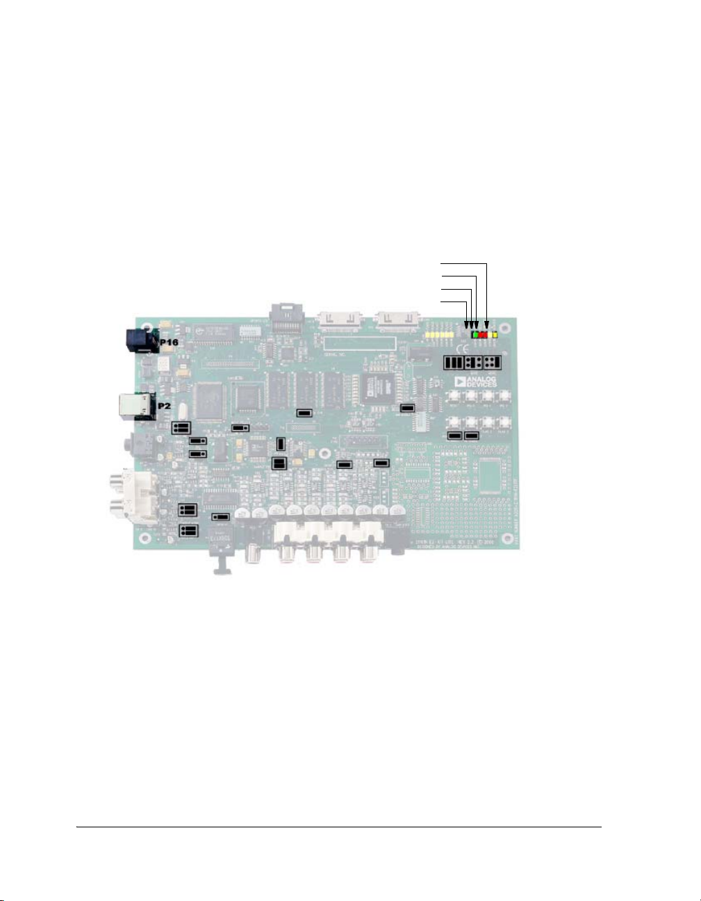
board carefully to avoid the discharge of static electricity, which may damage some components. Figure 1-1 shows the default jumper settings, DIP
switch, connector locations, and LEDs used in installation. Confirm that
your board is set up in the default configuration before using the board.
USB Monitor: LED10
DSP Reset: LED8
Reset: LED1
Power: LED11
Figure 1-1. EZ-KIT Lite Hardware Setup
1-4 ADSP-21161N EZ-KIT Lite Evaluation System Manual
Page 29

Installation and Session Startup
Using EZ-KIT Lite
L
For correct operation, install the software and hardware in the
order presented in the VisualDSP++ Installation Quick Reference
Card.
1. Verify that the yellow USB monitor LED (
USB connector) is lit. This signifies that the board is communicating properly with the host PC and is ready to run VisualDSP++.
2. From the Start menu, navigate to the VisualDSP++ environment
via the Programs menu.
If you are running VisualDSP++ for the first time, the New Session
dialog box appears on the screen (skip the rest of the procedure and
go to step 3).
If you have run VisualDSP++ previously, the last opened session
appears on the screen.
To switch to another session, via the Session List dialog box, hold
down the Ctrl key while starting VisualDSP++ (go to step 5).
3. In Debug target, select EZ-KIT Lite (ADSP-21xxx).
In Platform, select ADSP-21xxx EZ-KIT Lite.
In Processor, choose the appropriate processor, ADSP-21161.
In Session name, type a new name or accept the default.
LED10, located near the
4. Click OK to return to the Session List.
5. Highlight the session and click Activate.
ADSP-21161N EZ-KIT Lite Evaluation System Manual 1-5
Page 30

Evaluation License Restrictions
Evaluation License Restrictions
The ADSP-21161N EZ-KIT Lite installation is part of the VisualDSP++
installation. The EZ-KIT Lite is a licensed product that offers an unrestricted evaluation license for the first 90 days. Once the initial
unrestricted 90-day evaluation license expires:
• VisualDSP++ allows a connection to the ADSP-21161N EZ-KIT
Lite via the USB Debug Agent interface only. Connections to simulators and emulation products are no longer allowed.
• The linker restricts a users program to 5K words of internal memory for code space with no restrictions for data space.
Refer to the VisualDSP++ Installation Quick Reference Card for details.
Memory Map
The ADSP-21161N processors includes 1 Mbit of internal SRAM for program storage or data storage. The configuration of internal SRAM is
detailed in the ADSP-21161 SHARC Processor Hardware Reference.
The ADSP-21161N EZ-KIT Lite board contains 512K x 8-bits of external flash memory. The flash memory is connected to the processors’s
and
~BMS memory select pins. The flash memory can be accessed in either
the boot memory space or the external memory space. The external memory interface also connects to 1M x 48-bit SDRAM memory. The flash
memory connects to the
~MS0 pin.
~MS1
SDRAM Memory
To use the SDRAM memory, set the two SDRAM control registers to the
values shown in Listing 1-1.
1-6 ADSP-21161N EZ-KIT Lite Evaluation System Manual
Page 31

Table 1-1. EZ-KIT Lite Evaluation Board Memory Map
Start Address End Address Content
0x0000 0000 0x0001 FFFF IOP Registers (Internal)
0x0002 0000 0x0002 1FFF Block 0 Long Word Addressing
Using EZ-KIT Lite
Internal
Memory
External
Memory
0x0002 8000 0x0002 9FFF Block 1 Long Word Addressing
0x0004 0000 0x0004 3FFF Block 0 Normal Word Addressing
0x0005 0000 0x0005 3FFF Block 1 Normal Word Addressing
0x0008 0000 0x0008 7FFF Block 0 Short Word Addressing
0x000A 0000 0x000A 7FFF Block 1 Short Word Addressing
0x0010 0000 0x001F FFFF Multi-processor Memory Space
0x0020 0000 0x002F FFFF External Memory Space Bank 0 (SDRAM)
0x0400 0000 0x047F FFFF External Memory Space Bank 1 (FLASH)
0x0800 0000 0x0BFF FFFF External Memory Space Bank 2
0x0C00 0000 0x0FFF FFFF External Memory Space Bank 3
Listing 1-1. ADSP-21161N EZ-KIT Lite – SDRAM Settings
/* SDRAM Controller Setup for the ADSP-21161N EZ-KIT Lite */
/* Assumes SDRAM part# Micron MT48LC16M16A1-7SE (1Mx16-bit,
2 banks) */
/* Default Factory Hardware settings (rev2.3) */
/* LK_CFG[1:0]= 10,~CLDBL=1 */
/* CLKIN=25 MHz, => CCLK=100 MHz */
/* 3 SDRAMs by 16 bits wide total = 3x(1Mx16-bit) = 1M x 48-bit */
/* Mapped to MS0 addresses 0x00200000-0x002fffff */
/* Estimated SDCLK 50 MHz => SDCKR=0 */
/* Settings must be double counted for SDCKR-bit=0, except CAS
Latency) */
/* 50 MHz min @ CL=2 -> SDCL=2 [CAS Latency] */
/* tRAS=42ns min -> SDTRAS=5*2=10 [precharge delay] */
ADSP-21161N EZ-KIT Lite Evaluation System Manual 1-7
Page 32

SDRAM Memory
/* tRP=21ns min -> SDTRP=3*2=6 [active delay] */
/* tRCD=20ns min -> SDTRCD=2*2=4 [CAS-to-RAS delay] */
/* tREF=64ms/4K rows -> */
/* -> SDRDIV= (100MHz*64ms/4096) – 13 = 1549 = 0x60D cycles */
/* Note: If you change any clock, you have to change all settings
for best performance */
init_21161_SDRAM_controller:
ustat1=dm(WAIT);
bit clr ustat1 0x000FFFFF; /* clear MS0 wait state count */
dm(WAIT)=ustat1;
ustat1=0x60D; /* refresh rate
dm(SDRDIV)=ustat1;
ustat1=0x040146A2; /* mask in SDRAM settings */
dm(SDCTL)=ustat1;
init_21161_SDRAM_controller.end:
rts;
*/
When you are in a VisualDSP++ session connected to the ADSP-21161N
EZ-KIT Lite board, the SDRAM registers are configured automatically
through the debugger each time the processor is reset. Clearing the Auto
configure external memory check box on the Target Options dialog box,
which is accessible through the Settings pull-down menu, disables this
feature. For more information see “Target Options” on page 1-13.
1-8 ADSP-21161N EZ-KIT Lite Evaluation System Manual
Page 33

Using EZ-KIT Lite
FLAG Pins
The ADSP-21161N holds 12 asynchronous FLAG IO pins. Ten of these
pins (
FLAG0–9) are available for interaction with the running program.
After the processor is reset, the FLAGs are configured as inputs. The directions of the FLAGs are configured though the
and read though the
FLAG registers. The FLAG registers are summarized in
Table 1-2. For more information on FLAGs, refer to the ADSP-21161
SHARC Processor Hardware Reference.
Table 1-2. FLAG Pin Summary
MODE2 register and are set
1
FLAG
FLAG0 SW1/AD1836_SPI_SELECT FLAG0 connects to push button SW1 for user
FLAG1 SW2/AD1852_SPI_SELECT FLAG1 connects to push button SW2 for user
FLAG2 SW3 FLAG2 connects to push button SW3 for user
FLAG3 SW4 FLAG3 connects to push button SW4 for user
FLAG4–FLAG9 LED2–LED7 FLAG4–9 connect to LEDs on the EZ-KIT Lite
FLAG10 and
FLAG11
1 FLAG0–FLAG3 are available on connector P10.
Connects To Description
input and to the
audio codec.
input and to the
auxiliary DAC.
input.
input.
board and are for user output.
Not connected Not available
SPI select pin on the AD1836
SPI select pin on the AD1852
ADSP-21161N EZ-KIT Lite Evaluation System Manual 1-9
Page 34

Interrupt Pins
Interrupt Pins
The ADSP-21161N holds three interrupt pins (IRQ0–2) that let you interact with the running program. Each of the three external interrupts is
directly accessible through the push button switches
Lite board. Interrupt pins are summarized in Table 1-3. For more infor-
mation, refer to the ADSP-21161 SHARC Processor Hardware Reference.
Table 1-3. Interrupt Pin Summary
SW5–7 on the EZ-KIT
Interrupt
IRQ0 SW5 IRQ0–2 connect to the push buttons and supply
IRQ1 SW6
IRQ2 SW7
1 IRQ0–3 are available on connector P10.
1
Connects To Description
feedback for program execution. For instance, you
can write your code to trigger a FLAG when a
routine is complete.
Audio Interface
The audio interface consists of the AD1836 audio codec, the AD1852
auxiliary DAC and the CS8414 SPDIF receiver.
nect to the audio devices and provide 3 channels of stereo input (1
channel digital, 2 channels analog) and 4 channels of stereo output.
Analog audio input is facilitated by a 3.5 mm stereo jack (
RCA mono jacks (
P6). One of the AD1836 stereo input channels is dedi-
cated to two of the RCA mono jacks. The other stereo input channels can
either be supplied by the 3.5 mm stereo jack or the other two RCA mono
jacks.
JP11 determines which jack is used for audio input. Digital audio
input can be provided on either a single RCA mono jack (
input connector (
P4). JP2 determines the source. Three of the stereo out-
SPORT0 and SPORT2 con-
P7) and four
P5) or an optical
1-10 ADSP-21161N EZ-KIT Lite Evaluation System Manual
Page 35

Using EZ-KIT Lite
put channels come from the AD1836, while the final channel is from the
AD1852. See “Audio Connectors (P4–8, P17)” on page 2-18 for more
information about the connectors.
The AD1836 multi-channel codec features six digital-to-analog converters
(DACs) and four analog-to-digital converters (ADCs) and supports multiple digital stereo channels with 24-bit conversion resolution and a 96 kHz
sample rate. The AD1836 features a 108 dB dynamic range for each of its
six DACs and a 104 dB dynamic range for its four ADCs. The AD1836 is
configured through its SPI port. The ADSP-21161N processor is capable
of accessing the AD1836’s SPI port through the SPI port as well as
through
SPORT1. For more information, see “AD1836 Control Selection
Jumper (JP23)” on page 2-12.
The AD1852 is a complete 18/20/24-bit single-chip stereo digital audio
playback system. It is comprised of a multibit sigma-delta modulator, digital interpolation filters, and analog output drive circuitry. Other features
include an on-chip stereo attenuator and mute, programmed through an
SPI-compatible serial control port. The AD1852 is fully compatible with
all known DVD formats, including 192 kHz and 96 kHz sample frequencies and 24 bits. It also is backwards compatible by supporting 50/15µs
digital de-emphasis intended for “redbook” Compact Discs, as well as
de-emphasis at 32 kHz and 48 kHz sample rate.
The CS8414 is a monolithic CMOS device that receives and decodes
audio data up to 96 kHz, according to the AES/EBU, IEC958, S/PDIF,
and EIAJ CP340/1201 interface standards. The CS8414 receives data
from a transmission line, recovers the clock and synchronization signals,
and de-multiplexes the audio and digital data. The CS8414 is setup to
operate in Two-Wire Interface (TWI) compatible mode.
The
Microphone and Line-In jacks connect to the left and right ADC1
channel on the AD1836, depending on the setting of jumpers. See “MIC
Gain Selection Jumpers (JP9–10)” on page 2-8 and “ADC1 Input Selection Jumper (JP11)” on page 2-9 for more information. Two RCA jacks
ADSP-21161N EZ-KIT Lite Evaluation System Manual 1-11
Page 36

Example Programs
connect to
ADC2 on the AD1836. This input is configured though the
input mode selection jumpers, See “ADC2 Input Mode Selection Jumpers
(JP7–8)” on page 2-8 for more information.
The
Line-Out jacks connect to the left and right DAC outputs of the
AD1836 and AD1852.
The CS8414 includes an error flag (
put may not be valid. This signal connects to a LED (
VERF) to indicate that the audio out-
LED9) on the board.
This signal may also be used by interpolation filters to provide error
correction.
Example Programs
Example programs are provided with the ADSP-21161N EZ-KIT Lite to
demonstrate various capabilities of the evaluation board. These programs
are installed with the EZ-KIT Lite software and can be found in the
\…\211xx\EZ-KITs\ADSP-21161N\Examples subdirectory of the Visu-
alDSP++ installation directory. Please refer to the readme file provided
with each example for more information.
Flash Programmer Utility
The ADSP-21161N EZ-KIT Lite evaluation system includes a Flash Programmer utility. The utility allows you to program the flash memory on
the EZ-KIT Lite. The Flash Programmer is installed with VisualDSP++.
Once the utility is installed, it is accessible from the Tools pull-down
menu.
For more information on the Flash Programmer utility, go to online Help.
1-12 ADSP-21161N EZ-KIT Lite Evaluation System Manual
Page 37

Using EZ-KIT Lite
VisualDSP++ Interface
This section provides information about the following parts of the VisualDSP++ graphical user interface:
• “Boot Load” on page 1-13
• “Target Options” on page 1-13
• “Core Hang Conditions” on page 1-15
• “Restricted Software Breakpoints” on page 1-16
Boot Load
Choosing Boot Load from the Settings menu runs the processor and performs a hard reset on the board. This command saves you from having to
shut down VisualDSP++, reset the EZ-KIT Lite board, and bring up VisualDSP++ again when you want to perform a hard reset.
Use this feature when loading debug boot code from an external part or
when you want to put the device into a known state.
Target Options
Choosing Target Options from the Settings menu opens the Target
Options dialog box (Figure 1-2). Use target options to control certain
aspects of the processor on the ADSP-21161N EZ-KIT Lite evaluation
system.
While Target is Halted and On Emulator Exit Options
This target option controls the processor’s behavior when VisualDSP++
relinquishes processor control (for example, when exiting VisualDSP++).
The options are detailed in Table 1-4 and Table 1-5.
ADSP-21161N EZ-KIT Lite Evaluation System Manual 1-13
Page 38

VisualDSP++ Interface
Figure 1-2. Target Options Dialog Box
Table 1-4. While Target is Halted Options
Option Description
Stop I/O DMA Stops IO DMAs in emulator space. This option disables DMA requests when
the emulator has control of the processor. Data in the EP, LINK, or SPORT
DMA buffers are held there unless the internal DMA request was already
granted. This option holds off incoming data and ceases outgoing data. Because
SPORT-receive data cannot be held off, it is lost, and the overrun bit is set. The
direct write buffer (internal memory write) and the EP pad buffer are allowed
to flush any remaining data to internal memory.
Table 1-5. On Emulator Exit Options
Option Description
On Emulator
Exit
Determines the state the processor is left in when the emulator relinquishes control of the processor:
Reset DSP and Run causes the processor to reset and begin execution from its
reset vector location.
Run from current PC causes the processor to begin running from its current
location.
1-14 ADSP-21161N EZ-KIT Lite Evaluation System Manual
Page 39

Other Options
Table 1-6 describes other available target options.
Table 1-6. Other Target Options
Option Description
Using EZ-KIT Lite
Verify all writes to target
memory
Reset cycle counters on
run
Auto configure external
memory
Validates all memory writes to the processor. After each write, a read
is performed and the values are checked for a matching condition.
Enable this option during initial program development to locate
and fix initial build problems (such as attempting to load data into
non-existent memory).
Clear this option to increase performance while loading executable
files since VisualDSP++ does not perform the extra reads that are
required to verify each write.
Resets the cycle count registers to zero before a Run command is
issued. Select this option to count the number of cycles executed
between breakpoints in a program.
Enables the automatic configuration of the SDRAM registers (done
through the debugger).
Core Hang Conditions
Certain peripheral devices, such as host ports, DMA, and link ports, can
hold off the execution of processor instructions. This is known as a hung
condition and commonly occurs when reading from an empty port or
writing to a full port. If an attempt to halt the processor is made during
one of these conditions, the EZ-KIT Lite may encounter a core hang.
Normally, a core hang can be cleared by the board using a special
clear/abort bit. However, there are cases in which it is desirable or possible
not to clear the core hang. Sometimes it is desirable to wait for the core
hang to clear itself, such as when waiting for a host processor to read or
write data. In other cases, it is not possible to clear the core hang, and a
processor reset must occur to continue the debugging session.
Table 1-7 describes the EZ-KIT Lite’s core hang operations.
ADSP-21161N EZ-KIT Lite Evaluation System Manual 1-15
Page 40

VisualDSP++ Interface
Table 1-7. Core Hang Operations
Option Description
Abort Abort the hung operation. This causes the offending instruction to be
aborted in the pipeline.
Retry Allows you to remedy the hung operation. For example, if a host proces-
sor is holding off the processor, you can cause the host to clear the hung
condition.
Ignore Performs a software reset on the target board.
Clear Aborts the hung operation. This causes the offending instruction to be
aborted in the pipeline.
Acknowledge Allows you to remedy the hung operation. For example, if a host proces-
sor is holding off the processor, you can cause the host to clear the hung
condition.
Reset Performs a software reset on the target board.
Restricted Software Breakpoints
The EZ-KIT Lite development system restricts breakpoint placement
when certain conditions are met. That is, under some conditions, breakpoints cannot be placed effectively. Such conditions depend on bus
architecture, pipeline depth, and ordering of the EZ-KIT Lite and its target processor.
1-16 ADSP-21161N EZ-KIT Lite Evaluation System Manual
Page 41

2 EZ-KIT LITE HARDWARE
REFERENCE
This chapter describes the hardware design of the ADSP-21161N EZ-KIT
Lite board. The following topics are covered.
• “System Architecture” on page 2-2
Describes the configuration of the ADSP-21161N EZ-KIT Lite
board and explains how the board components interface with the
processor.
• “Jumper Settings” on page 2-5
Shows the location and describes the function of the on-board
jumpers.
• “LEDs and Push Buttons” on page 2-13
Shows the location and describes the function of the LEDs and
push buttons.
• “Connectors” on page 2-16
Shows the location and gives the part number for the on-board
connectors. Also, the manufacturer and part number information is
given for the mating parts.
• “Specifications” on page 2-21
Provides the board’s measurements and power supply
specifications.
ADSP-21161N EZ-KIT Lite Evaluation System Manual 2-1
Page 42

System Architecture
System Architecture
This section describes the processor’s configuration on the EZ-KIT Lite
board.
Figure 2-1. System Architecture Block Diagram
The ADSP-21161N processor’s core voltage is 1.8V, and the external
interface voltage is 3.3V.
A 25 MHz through-hole oscillator supplies the input clock to the processor. Footprints are provided on the board for a surface-mount oscillator
and a through-hole crystal for alternate user-installed clocks. The speed at
2-2 ADSP-21161N EZ-KIT Lite Evaluation System Manual
Page 43

EZ-KIT Lite Hardware Reference
which the core operates is determined by the location of the clock mode
jumper (
JP21) as described on page 2-11. By default, the processor core
runs at 100 MHz.
External Port
The External Port (EP) of the processor connects to a 512K x 8-bit flash
memory. The flash memory connects to the boot memory select (
pin and the memory select 1 (
memory to be used to boot the processor as well as to store information
during normal operation.
The external memory interface also connects to 1M x 48-bit SDRAM
memory. The SDRAM memory connects to the memory select 0 (
pin. Refer to “SDRAM Disable Jumper (JP1)” on page 2-5 for information on how to configure the width of the SDRAM. Refer to “SDRAM
Memory” on page 1-6 for a summary of the processor’s memory map.
~MS1) pin. The connection allows the flash
~BMS)
~MS0)
Some of the address, data, and control signals are available externally via
two off-board connectors. The EP connectors’ pinout (
P9 and P10) can be
found in Appendix B, “Schematics”.
Host Processor Interface (HPI)
The Host Port Interface (HPI) signals are brought to an unpopulated
off-board connector (
P9). This allows the HPI to interface with a user
application. The pinout of the host port connector can be found in
Appendix B, “Schematics”.
SPORT Audio Interface
SPORT0 and SPORT2 are connected to the AD1836 codec (U10). A 3.5 mm
stereo jack and four RCA mono jacks facilitate an audio input, while a
3.5 mm stereo jack and eight RCA mono jacks facilitate an audio output.
ADSP-21161N EZ-KIT Lite Evaluation System Manual 2-3
Page 44

System Architecture
The codec contains two input channels. One channel connects to a
3.5 mm stereo jack and two RCA jacks. The 3.5 mm stereo jack connects
to a microphone. The two RCA jacks can connect to a
LINE-OUT from an
audio device. You can supply an audio input to the codec microphone
input channel (
of
JP11 determine whether the LINE_IN channel of the codec is driven by
the
P6 connector or by the P7 connector.
MIC1) or to the LINE_IN input channel. The jumper settings
SPI Audio Interface
The SPI port is connected to the AD1836 and AD1852. The SPI port is
used for writing and reading the control registers of the audio devices.
Breadboard Area
Use the breadboard area to add external circuitry to:
• All board voltages and grounds
• Package footprints:
D 1x SOIC16
D 1x SOIC20
D 4x SOT23-6
D 1x PSOP44
D 2x SOT23
D 27x 0805
Analog Devices does not support and is not responsible for the
[
effects of additional circuitry.
2-4 ADSP-21161N EZ-KIT Lite Evaluation System Manual
Page 45

EZ-KIT Lite Hardware Reference
JTAG Emulation Port
The JTAG emulation port allows an emulator to access the processor’s
internal and external memory, as well as the special function registers,
through a 14-pin header.
For a detailed description of the interface’s connectors, see EE-68 published on the Analog Devices website. For more information, see “JTAG
Connector (P12)” on page 2-19. For more information about available
emulators, contact Analog Devices (see “Product Information”).
Jumper Settings
This section describes the function of all the jumpers. Figure 2-2 shows
the locations of all the jumpers.
SDRAM Disable Jumper (JP1)
The JP1 jumper is used to enable or disable the third SDRAM device.
When the jumper is installed, the ADSP-21161N can access the SDRAM
as 48-bit-wide external memory.
The upper 16 bits of data are multiplexed with the Link Ports and the
external data bus; therefore, when the jumper is installed, the Link Ports
are not available. To use the Link Ports, the
JP1 jumper must be removed.
SPDIF Selection Jumper (JP2)
The JP2 jumper is used select the SPDIF input to the CS8414 digital
audio receiver. When the jumper is configured for an optical connection,
the TOSLINK optical input connector (
jumper is configured for a coax connection, the RCA input connector (
should be used.
ADSP-21161N EZ-KIT Lite Evaluation System Manual 2-5
P4) should be used. When the
P5)
Page 46

Jumper Settings
e
D
m
p
e
p
JP11: ADC1 In
JP5: FLAG1 Enabl
JP1: External Memory
Width
JP22: BMS Enable
JP19: DSP I
JP20: Boot Mod
JP21: Clock Mode
JP26: SW1 Enable
JP27: SW2 Enable
JP4: FLAG0 Enable
JP23: AD1836 Control Select
JP6: Sa
JP3: MCLK Select
JP2: SPDIF Select
JP9: Mic Gain Right
JP10: Mic Gain Left
JP7: ADC2 Input Mode Left
JP8: ADC2 Input Mode Right
ut Selector
le Frequency
Figure 2-2. Jumper Locations
MCLK Selection Jumper (JP3)
The JP3 jumper is used to select the MCLK source for the AD1836 and
AD1852.
2-6 ADSP-21161N EZ-KIT Lite Evaluation System Manual
Page 47

EZ-KIT Lite Hardware Reference
Table 2-1. SPDIF Modes
Jumper Location Mode
1 and 2 Optical (factory default)
2 and 3 Coax
Table 2-2. MCLK Selection
Jumper Location MCLK Source
1 and 2 Audio Oscillator (12.288 MHz) (factory default)
2 and 3 Derived clock from SPDIF Stream
FLAG0 Enable Jumper (JP4)
In standard configuration, FLAG0 is connected to the AD1836 and used as
a select for the SPI port. This jumper should be removed to use the push
button switch or the signal on the expansion connector (
jumper is removed, the SPI can no longer communicate with the
AD1836.
P10). Once the
FLAG1 Enable Jumper (JP5)
In standard configuration, FLAG1 is connected to the AD1852 and used as
a select for the SPI port. The
push button switch or the signal on the expansion connector (
JP5 jumper should be removed to use the
P10). Once
the jumper is removed, the SPI can no longer communicate with the
AD1852.
Sample Frequency Jumper (JP6)
The JP6 jumper is used to select the sample frequency for the AD1852
device. Table 2-3 shows the valid frequency modes.
ADSP-21161N EZ-KIT Lite Evaluation System Manual 2-7
Page 48

Jumper Settings
Table 2-3. Sample Frequencies
Jumper Location Sample Frequency
None installed Not allowed
3 and 4 192 kHz (2x Interpolator)
1 and 2 96 kHz (4x Interpolator)
1 and 2, 3 and 4 48 kHz (8x Interpolator) (factory default)
ADC2 Input Mode Selection Jumpers (JP7–8)
The JP7 and JP8 jumpers control the input mode to ADC2 on the
AD1836 (see Table 2-4). In high-performance mode, the signal is routed
straight in to the ADC. In PGA mode, the signal goes through a multiplexer and a programmable gain amplifier inside of the codec.
Table 2-4. ADC Input Mode
Jumper Location Input Mode
3 and 5, 4 and 6 PGA (factory default)
1 and 3, 2 and 4 High Performance
MIC Gain Selection Jumpers (JP9–10)
The JP9 and JP10 jumpers are used to select the pre-amp gain for the
microphone circuit (see Table 2-5). The gain for the left and right channel
should be configured the same.
Table 2-5. MIC Pre Amp Gain
Jumper Position Gain
Not Installed 0 dB
2-8 ADSP-21161N EZ-KIT Lite Evaluation System Manual
Page 49

EZ-KIT Lite Hardware Reference
J
Table 2-5. MIC Pre Amp Gain (Cont’d)
Jumper Position Gain
1 and 2 20 dB
2 and 3 40 dB (factory default)
ADC1 Input Selection Jumper (JP11)
The JP11 jumper is used to select the input source for ADC2. If the input
source for ADC2 is
If the input source for ADC2 is a microphone, then the mini stereo plug
P7 should be used. If a microphone is used, the gain of the circuit may be
increased, as described in “MIC Gain Selection Jumpers (JP9–10)” on
page 2-8.
LINE-IN, then the RCA connector P6 should be used.
When the
4, the connection is to
and between pins 4 and 6, the connection is to
JP11 jumpers are between pins 1 and 3 and between pins 2 and
P7. When the jumpers are between pins 3 and 5
P6. The jumper settings are
illustrated in Table 2-6). (The words MIC and LINE are on the board as a
reference.)
Table 2-6. Audio Input Jumper Settings
Microphone Input Stereo LINE_IN (Default)
1 2
1 2
P11
ADSP-21161N EZ-KIT Lite Evaluation System Manual 2-9
Page 50

Jumper Settings
Processor ID Jumper (JP19)
The JP19 jumper is used to select a different ID for the processor. During
typical operation of the EZ-KIT Lite board, there is only a single processor in the system. The jumper should be set to the single processor setting.
When a second processor is attached to the board though the link port,
these jumpers should be changed to configure one board for processor 1
and the other board for processor 2. System configuration options are
shown in Table 2-7.
Table 2-7. Processor ID Modes
Jumper Position Description
1 and 2, 3 and 4, 5 and 6 Single processor (default)
3 and 4, 5 and 6 Processor 1
1 and 2, 5 and 6 Processor 2
Other Invalid
Boot Mode Selection Jumper (JP20)
The JP20 jumper determines how the ADSP-21161N processor boots.
Table 2-8 shows the jumper setting for the processor boot modes.
Table 2-8. Boot Mode Select Jumper (JP20) Settings
EBOOT
Pins 1 & 2
Not installed Installed Not installed
Installed Installed Not installed
Installed Not installed Installed (input) Serial Boot via SPI
2-10 ADSP-21161N EZ-KIT Lite Evaluation System Manual
LBOOT
Pins 3 & 4
BMS
Pins 5 & 6
(output)
(input)
Processor Boot Mode
EPROM BOOT (default)
Host Processor Boot
Page 51

EZ-KIT Lite Hardware Reference
Table 2-8. Boot Mode Select Jumper (JP20) Settings (Cont’d)
EBOOT
Pins 1 & 2
Installed Not installed Not installed
Installed Installed Installed (input) No Boot
Not installed Not installed Installed (input) Reserved
LBOOT
Pins 3 & 4
BMS
Pins 5 & 6
(input)
Processor Boot Mode
Link Port Boot
Clock Mode Selection Jumper (JP21)
The JP21 jumper controls the speed for the core and external port of the
ADSP-21161N processor. The frequency supplied to CLKIN of the processor may be changed by removing the 25 MHz oscillator (
shipped with the board and replacing it with a different oscillator or crystal (
Y2). A clock mode and frequency should be selected so that the
minimum and maximum specs of the ADSP-21161N processor are not
exceeded. For more information on clock modes, see the ADSP-21161
SHARC Processor Hardware Reference. Table 2-9 shows the jumper setting
for the clock modes.
Table 2-9. Clock Mode Selections
U24) that is
CLKDBL
Pins 1 & 2
Not installed Installed Installed 2:1 1x
Not installed Installed Not installed 3:1 1x
Not installed Not installed Installed 4:1 1x (default)
Installed Installed Installed 4:1 2x
Installed Installed Not installed 6:1 2x
Installed Not installed Installed 8:1 2x
CLK_CFG1
Pins 3 & 4
CLK_CFG0
Pins 5 & 6
Core Clock
Ratio
External Port
Clock Ratio
ADSP-21161N EZ-KIT Lite Evaluation System Manual 2-11
Page 52

Jumper Settings
~BMS Enable Jumper (JP22)
The JP22 jumper is used to control the routing of the Boot Memory Select
~BMS) signal. When the jumper is installed, the ~BMS signal is routed to
(
the flash memory interface and can be used for reading, writing, and booting. The jumper should be installed when using EPROM boot mode. The
jumper should be removed when using the serial boot or no-boot mode. If
the jumper remains “
ON” in serial boot or no-boot modes, the ~BMS signal
is grounded, and the flash memory is selected.
AD1836 Control Selection Jumper (JP23)
The AD1836 control registers are programmed through an SPI port. The
SPI port can be configured to be connected to the processor’s SPI port or
SPORT1. When the jumper is installed at JP23, the AD1836 SPI port is
connected to
AD1836 SPI port connects to the processor’s SPI port. By default, the
jumper is installed.
SPORT1 of the processor. When the jumper is removed, the
SW1 Enable Jumper (JP26)
The SW1 push button is attached though a driver to FLAG0 of the processor.
To disconnect the driver from
put), remove
JP26.
FLAG0 (for example, to use FLAG1 as an out-
SW2 Enable Jumper (JP27)
The SW2 push button is attached though a driver to FLAG1 of the processor.
To disconnect the driver from (for example, to use
remove
JP27.
2-12 ADSP-21161N EZ-KIT Lite Evaluation System Manual
FLAG1 as an output),
Page 53

EZ-KIT Lite Hardware Reference
LEDs and Push Buttons
This section describes the functionality of the LEDs and push buttons.
Figure 2-3 shows the locations of the LEDs and push buttons.
USB Monitor: LED10
VERF: LED9
DSP Reset: LED8
Reset: LED1
Power: LED11
FLAG4-9: LED2 - 7
Reset: SW8
IRQ0-2: SW5-7
FLAG0-3: SW1-4
Figure 2-3. LED and Push Button Locations
ADSP-21161N EZ-KIT Lite Evaluation System Manual 2-13
Page 54

LEDs and Push Buttons
Reset LEDs (LED1 and LED8)
When LED1 is lit, the master reset of all the major ICs is active.
When
LED8 is lit, the ADSP-21161N processor (U1) is being reset. The
USB interface resets the processor during USB communication
initialization.
FLAG LEDs (LED2–7)
The FLAG LEDs connect to the processor’s flag pins (FLAG4–9). The
LEDs are active
Refer to “LEDs and Push Buttons” on page 2-13 for more information on
how to use the programmable flags to program the processor. Table 2-10
shows the FLAG signals and the corresponding LEDs.
Table 2-10. FLAG LEDs
FLAG Pin LED Reference Designator
FLAG4 LED7
FLAG5 LED6
FLAG6 LED5
FLAG7 LED4
FLAG8 LED3
HIGH and are lit by an output of “1” from the processor.
FLAG9 LED2
VERF LED (LED9)
The VERF LED indicates that there is a possible error in the audio stream
of the CS8414 digital receiver. The error may occur when digital audio
cables disconnect from the optical or coaxial SPDIF connectors.
2-14 ADSP-21161N EZ-KIT Lite Evaluation System Manual
Page 55

EZ-KIT Lite Hardware Reference
USB Monitor LED (LED10)
The USB monitor LED (LED10) indicates that USB communication has
been initialized successfully, and you may connect to the processor using a
VisualDSP++ EZ-KIT Lite session. If the LED does not light, try cycling
power on the board and/or reinstalling the USB driver (see the Visu-
alDSP++ Installation Quick Reference Card).
L
Lite target board, the LED can flicker, indicating communications
handshake.
Power LED (LED11)
When VisualDSP++ is actively communicating with the EZ-KIT
When LED11 is lit (green), it indicates that power is being properly supplied to the board.
Programmable FLAG Push Buttons (SW1–4)
Four push buttons (SW1–4) are provided for general-purpose user input.
The push buttons connect to the processor’s
are active “
HIGH” and, when pressed, send a High (1) to the processor.
Refer to “FLAG Pins” on page 1-9 for more information. The push but-
ton reference designators and corresponding FLAGs are summarized in
Table 2-11.
Table 2-11. FLAG Switches
FLAG Pin Push Button Reference
Designator
FLAG Pin Push Button Reference
FLAG pins. The push buttons
Designator
FLAG0 SW1 FLAG2 SW3
FLAG1 SW2 FLAG3 SW4
ADSP-21161N EZ-KIT Lite Evaluation System Manual 2-15
Page 56

Connectors
Interrupt Push Buttons (SW5–7)
Three push buttons are provided for general-purpose user interrupts. SW5–
connect to the processor’s programmable FLAG pins. The push but-
SW7
tons are active “
processor. Refer to “FLAG Pins” on page 1-9 for more information. The
push button reference designators and corresponding interrupt signals are
summarized in Table 2-12.
Table 2-12. Interrupt Switches
Interrupt Signal Push Button Reference Designator
IRQ0 SW5
IRQ1 SW6
IRQ2 SW7
HIGH” and, when pressed, send a High (1) to the
Board Reset Push Button (SW8)
The RESET push button (SW8) resets all of the ICs on the board. During
reset, the USB interface is automatically reinitialized.
[
Pressing the RESET push button (SW8) while VisualDSP++ is running disrupts communication and causes errors in the current
debug session. VisualDSP++ must be closed and re-opened.
Connectors
This section describes the connector functionality and provides information about mating connectors. Figure 2-4 shows the connector locations.
USB Connector (P2)
The USB connector (P2) is a standard Type B USB receptacle.
2-16 ADSP-21161N EZ-KIT Lite Evaluation System Manual
Page 57

EZ-KIT Lite Hardware Reference
Figure 2-4. Connector Locations
Part Description Manufacturer Part Number
Type B USB receptacle Mill-Max 897-30-004-90-000
Digi-Key ED90003-ND
Mating Connector (provided with the EZ-KIT Lite)
USB cable Assmann AK672-5
Digi-Key AK672-5ND
ADSP-21161N EZ-KIT Lite Evaluation System Manual 2-17
Page 58

Connectors
Audio Connectors (P4–8, P17)
There are two 3.5 mm stereo audio jacks, 13 RCA jacks, and one optical
connector.
Part Description Manufacturer Part Number
3.5 mm stereo jack (P7 and P17) Shogyo SJ-0359AM-5
RCA Jacks (P6) SWITCHCRAFT PJRAS2X2S01
RCA Jacks (
TORX (P4) TOSHIBA TORX173
Coaxial (P5) SWITCHCRAFT PJRAN1X1U01
3.5mm stereo plug to 3.5mm stereo
cable (
Two channel RCA interconnect cable
(
P6 and P8)
Digital Fiber-Optic Cable (P4) Monster Cable ILS100-1M
Digital Coaxial Cable (P5) Monster Cable IDL100-1M
P8) SWITCHCRAFT PJRAS4X2U01
Mating Connectors
Radio Shack L12-2397A
P7 and P17)
Monster Cable BI100-1M
External Port Connector (P9)
A 40-pin 0.05' spacing connector provides access to some of the processor’s External Port signals. By default, this connector is not populated.
Part Description Manufacturer Part Number
40-pin 0.05’ (male) Samtec FTSH-120-01-F-D-K
Mating Connector
Female to female cable Samtec FFSD-20-D-5.000-01-N
2-18 ADSP-21161N EZ-KIT Lite Evaluation System Manual
Page 59

EZ-KIT Lite Hardware Reference
Host Processor Interface Connector (P10)
A 20-pin 0.05' spacing connector provides access to some of the processor’s External Port signals. By default, this connector is not populated.
Part Description Manufacturer Part Number
20-pin 0.05’ (male) Samtec FTSH-110-01-F-D-K
Mating Connector
Female to female cable Samtec FFSD-10-D-5.000-01-N
JTAG Connector (P12)
The JTAG header (P12) is the connecting point for a JTAG in-circuit
emulator pod. When an emulator is connected to the JTAG header, the
USB debug interface is disabled.
Pin 3 is missing to provide keying. Pin 3 in the mating connector should
have a plug.
L
Part Description Manufacturer Part Number
14-pin IDC Header (P12) Berg 54102-T08-07
When using an emulator with the EZ-KIT Lite board, follow the
connection instructions provided with the emulator.
Link Port Connectors (P13–14)
Each link port is connected to a 26-pin connector. Refer to EE-106 found
on the ADI website at http://www.analog.com for more information
about the link port connectors.
ADSP-21161N EZ-KIT Lite Evaluation System Manual 2-19
Page 60

Connectors
Part Description Manufacturer Part Number
26 position connector Honda RMCA-26JL-AD
Mating Connector
Cable connector Honda RMCA-E26F1S-A
Shroud Honda RMCA-E26L1A
Coaxial cable Gore DXN2132
SPORT1 and SPORT3 Connector (P15)
SPORT1 and SPORT3 are connected to a 20-pin connector.
Part Description Manufacturer Part Number
20 position AMPMODU system 50
receptacle
20 position AMPMODU system 20
connector
20 position AMPMODU system 20
connector (w/o lock)
Flexible film contacts (20 per connector)
AMP 104069-1
Mating Connector
AMP 2-487937-0
AMP 2-487938-0
AMP 487547-1
Power Connector (P16)
The power connector (P16) provides all of the power necessary to operate
the EZ-KIT Lite board.
Part Description Manufacturer Part Number
2.5 mm Power Jack (
P16) SWITCHCRAFT RAPC712
Digi-Key SC1152-ND
2-20 ADSP-21161N EZ-KIT Lite Evaluation System Manual
Page 61

EZ-KIT Lite Hardware Reference
Part Description Manufacturer Part Number
Mating Power Supply (shipped with EZ-KIT Lite)
5V Power Supply CUI Stack DTS070175SUDC-p6-SZ
Specifications
This section provides the requirements for powering the board.
Power Supply
The power connector supplies DC power to the EZ-KIT Lite board.
Table 2-13 shows the power supply specifications.
Table 2-13. Power Supply Specifications
Terminal Connection
Center pin +7V@2 amps
Outer Ring GND
Board Current Measurements
The ADSP-21161N EZ-KIT Lite board provides two zero-ohm resistors
that may be removed to measure current draw. Table 2-14 shows the resistor number, the voltage plane, and a description of the components on the
plane.
Table 2-14. Current Measurement Resistors
Resistor Voltage Plane Description
R168 VDDINT Core Voltage of the processor
R169 VDDEXT IO Voltage of the processor
ADSP-21161N EZ-KIT Lite Evaluation System Manual 2-21
Page 62

Specifications
2-22 ADSP-21161N EZ-KIT Lite Evaluation System Manual
Page 63

A BILL OF MATERIALS
The bill of materials corresponds to the board schematics on page B-1.
Please check the latest schematics on the Analog Devices website,
http://www.analog.com/Processors/Processors/DevelopmentTools/tec
hnicalLibrary/manuals/DevToolsIndex.html#Evaluation%20Kit%20Manuals
.
ADSP-21161N EZ-KIT Lite Evaluation System Manual A-1
Page 64

U5 ST MICRO M29W040B120K6
U21-22 TI 74LVC14AD
U2-4 MICRON MT48LC1M16A1TG-7S
U8 CIRRUS LOGIC CS8414
U6 CYPRESS CY7C64603-128NC
Q2 FAIRCHILD MMBT4124
Q1 FAIRCHILD MMBT4401
12.288MH
U30 CYPRESS CY7C1019BV33-12VC
U29 ANALOG DEVICES AD8532AR
U34,U37 TI SN74AHC1G02DBVR
FLASH-512K-X-8-3V
HEX-INVER-SCHMITT-TRIGGER
1MX16-SDRAM-143MHZ
96KHZ-DIGITAL-AUDIO-RECVR
USB-TX/RX MICROCONTROL-
LER
NPN TRANSISTOR 1A
Ref. # Description Reference Designator Manufacturer Part Number
1 1 M29W040 PLCC32
2 2 74LVC14A SOIC14
3 3 MT48LC1M16A1TG TSOP50
4 1 CS8414 SOIC28
5 1 CY7C64603-128 PQFP128
6 1 MMBT4124 SOT-23
NPN TRANSISTOR 200MA
7 1 MMBT4401 SOT-23
8 2 74LVC00AD SOIC14 U9, U27 PHILIPS 74LVC00AD
9 1 CY7C1019BV33-15VC SOJ32
128K X 8 SRAM
DUAL AMP 250MA
10 1 AD8532AR SOIC8
11 1 12.288MHZ 1/2 OSC001 U25 DIG01 SG-8002DC-PCC-ND
SINGLE-2 INPUT-NOR
12 2 SN74AHC1G02 SOT23-5
A-2 ADSP-21161N EZ-KIT Lite Evaluation System Manual
Page 65

AVX 12065A222JAT050
Bill Of Materials
U33 TI SN74LV164AD
8-BIT-PARALLEL-SERIAL
Ref. # Description Reference Designator Manufacturer Part Number
13 1 SN74LV164A SOIC14
U32 CYPRESS CY7C4201V-15AC
U24 DIGI-KEY SG-8002DC-PCC-ND
64-BYTE-FIFO
OSC
14 1 CY7C4201V-15AC TQFP32
15 1 25MHZ 1/2 OSC01
Y1 DIG01 300-6027-ND
CRYSTAL
16 1 12.0MHZ THR OSC006
U7 MICROCHIP 24LC00-SN
SEE 1000127
17 1 21161 24LC00 U7""
C85-86 AVX 12065A102JAT2A
CERM
18 2 1000pF 50V 5% 1206
C40, C46, C52, C58,
C64, C70, C76, C82
VOLTAGE-SUPERVISOR
NPO
20 1 ADM708SAR SOIC8
19 8 2200pF 50V 5% 1206
U10 ANALOG DEVICES AD1836AS
MULTIBIT-SIGMA-DELTA-DAC
21 1 AD1852 SSOP28
22 1 AD1836AS MQFP52
MULTI-CHAN-
NEL-96KHZ-CODEC
U1 ANALOG DEVICES ADSP-21161NCCA100
VR2 ANALOG DEVICES ADP3338AKC-3.3
1MM SPACING REV. X1.2
3.3V-1.0AMP REGULATOR
23 1 ADSP-21161NKCA100 PBGA225
24 1 ADP3338AKC-33 SOT-223
U26 ANALOG DEVICES ADM708SAR
U11 ANALOG DEVICES AD1852JRS
ADSP-21161N EZ-KIT Lite Evaluation System Manual A-3
Page 66

VR1, VR5 ANALOG DEVICES ADP3339AKC-5-REEL
VR3 ANALOG DEVICES ADP3338AKC-1.8
U12-20, U28 NATIONAL SEMI LMV722M
CT23-25 AVX TAJC475K025R
P16 SWITCHCRAFT SC1152-ND12
P2 MILL-MAX 897-30-004-90-000000
P4 TOSHIBA TORX173
P8 SWITCHCRAFT PJRAS4X2U01
P5 SWITCHCRAFT PJRAN1X1U01
RMCA-EA26LMY-0M03-A
(TSUSHINK)
P15 AMP 104069-1
5V-1.5A REGULATOR
1.8V-1A REGULATOR
DUAL AUDIO OP AMP
TAN T
RA
USB
FIBER OPTIC REV MODULE
RA
Ref. # Description Reference Designator Manufacturer Part Number
25 2 ADP3339AKC-5 SOT-223
26 1 ADP3338AKC-18 SOT-223
27 10 LMV722M SOIC8
28 3 4.7uF 25V 10% C
29 1 PWR 2.5MM_JACK CON005
30 1 USB 4PIN CON009
BLK
31 1 TORX173 6PIN CON008
32 1 RCA 4X2 CON011
33 1 RCA 1X1 CON012
34 1 RCA 2X2 CON013 P6 SWITCHCRAFT PJRAS2X2S01
35 2 LNKPRT 12X2 CON010 P13-14 HONDA
RA
36 1 .05 10X2 CON014
A-4 ADSP-21161N EZ-KIT Lite Evaluation System Manual
Page 67

Bill Of Materials
Ref. # Description Reference Designator Manufacturer Part Number
SW1-8 PANASONIC EVQ-PAD04M
6MM
37 8 SPST-MOMENTARY SWT013
38 1 DIP8 SWT016 SW9 C&K CKN1365-ND
YAGEO 0.0ECT-ND
R168-169, R217, R218
39 1 10 1/8W 5% 1206 R2 PANASONIC P10ECT-ND
40 6 0.00 1/8W 5% 1206 R153, R154,
AVX 08055A331JAT
LED2-7, LED9-10 PANASONIC LN1461C-TR
C36, C42, C48, C54,
C60, C66, C72, C78
GULL-WING
NPO
41 8 AMBER-SMT LED001
42 8 330pF 50V 5% 805
AVX 08055C104KAT
C154-155, C165-171,
C184-C186, C174-179
CERM
AVX 08053C224FAT
C1,C5,C9-11,
C156-164, C172,
C183
CERM
45 16 0.1uF 50V 10% 805
44 11 0.22uF 25V 10% 805
AVX 08051C103KAT2A
C2, C6-7, C91-149,
43 80 0.01uF 100V 10% 805
C33,C87-90,C150-153
CERM
, C173,C180
AVX 08055A102JAT2A
CT19-22, CT36 SPRAGUE 293D106X9025C2T
C14-15, C19-20,
C24-25, C29-30
TAN T
NPO
47 5 10uF 16V 10% C
46 8 0.001uF 50V 5% 805
ADSP-21161N EZ-KIT Lite Evaluation System Manual A-5
Page 68

AVX CR21-103J-T
-20,R124,R126,R128,
AVX CR21-4701F-T
R130, R132,R134,
R136, R148-149,
R151, R155-164,
R175, R177-181,
R183,R190,
R171,R172, R174,
R185-187, R193-194,
R219-220
R191, R165
AVX CR32-4992F-T
R98, R106, R114,
R122, R192, R206
Ref. # Description Reference Designator Manufacturer Part Number
48 47 10K 100MW 5% 805 R3-4,R6,R13,R15,R17
49 4 33 100MW 5% 805 R1, R150, R176, R152 AVX CR21-330JTR
50 5 4.7K 100MW 5% 805 R184, R188, R189,
51 11 680 100MW 5% 805 R137-147 AVX CR21-6800F-T
52 1 1M 100MW 5% 805 R12 AVX CR21-1004F-T
53 1 475 100MW 5% 805 R16 AVX CR21-471J-T
54 1 1.5K 100MW 5% 805 R7 AVX CR21-1501F-T
55 2 2.00K 1/8W 1% 1206 R49-50 DALE CRCW1206-2001FRT1
56 10 49.9K 1/8W 1% 1206 R66, R74, R82, R90,
57 2 2.21K 1/8W 1% 1206 R10-11 AVX CR32-2211F-T
A-6 ADSP-21161N EZ-KIT Lite Evaluation System Manual
Page 69

Bill Of Materials
AVX 12061A101JAT2A
C12, C16-17, C21-22,
C26-27, C31, C35,
NPO
Ref. # Description Reference Designator Manufacturer Part Number
58 24 100pF 100V 5% 1206
C38,
C41, C44, C47, C50,
C53, C56, C59, C62,
C65, C68,
CT1-4, CT11 AVX TAJB106K016R
C71, C74, C80, C77
TAN T
59 5 10uF 16V 10% B
60 1 22K 100MW 5% 805 R216 AVX CR21-223J-T
AVX CR21-101J-T
61 7 100 100MW 5% 805 R123, R125, R127,
AVX 12061A221JAT2A
C39, C45, C51, C57,
R135
62 8 220pf 50V 10% 1206
C63, C69, C75, C81
NPO
R129, R131, R133,
FER13 MURATA PLM250S40T1
D1-2 GENERALSEMI S2A
0.06 CHOKE
63 1 1000 100MHZ 1.5A FER002
64 2 2A S2A_RECT DO-214AA
SILICON RECTIFIER
FER1-11 DIGI-KEY 240-1019-1-ND
0.70 BEAD
65 11 600 100MHZ 500MA 1206
KOA P11.0FCT-ND
66 8 237 1/8W 1% 1206 R23, R27, R30, R34,
R40-41, R47-48
67 4 750K 1/8W 1% 1206 R25, R32, R38, R45 KOA RK73H2BT7503F
ADSP-21161N EZ-KIT Lite Evaluation System Manual A-7
Page 70

DALE CRCW12065761FRT1
R28-29, R31, R33,
R35-37, R39, R42-44,
DALE CRCW12061102FTR1
R46
PHILLIPS 1206CG121J9B200
C13, C18, C23, C28,
R91, R99, R107, R115
C187-190
R95, R103, R111,
R119
PANASONIC ERJ-8ENF5491V
R76, R77, R84, R85,
R92, R93, R100,
R101, R108, R109,
R116, R117
PANASONIC ERJ-8ENF2741V
AVX 08055A681FAT2A
C32, C34 AVX 12061A821KAT2A
C37, C43, C49, C55,
C61, C67, C73, C79
Ref. # Description Reference Designator Manufacturer Part Number
68 16 5.76K 1/8W 1% 1206 R21, R22, R24, R26,
69 8 11.0K 1/8W 1% 1206 R59, R67, R75, R83,
70 1 68NF 50V 10% 805 C8 MURRATA GRM40X7R683K050AL
NPO
71 8 120PF 50V 5% 1206
NPO
72 1 75 1/8W 5% 1206 R14 PHILIPS 9C12063A75R0JLRT/R
73 2 820PF 100V 10% 1206
74 2 30PF 100V 5% 1206 C3-4 AVX 12061A300JAT2A
75 8 680PF 50V 1% 805
NPO
76 8 2.74K 1/8W 1% 1206 R63, R71, R79, R87,
77 16 5.49K 1/8W 1% 1206 R60, R61, R68, R69,
A-8 ADSP-21161N EZ-KIT Lite Evaluation System Manual
Page 71

Bill Of Materials
PANASONIC ERJ-8ENF3321V
R94, R102, R110,
Ref. # Description Reference Designator Manufacturer Part Number
78 8 3.32K 1/8W 1% 1206 R62, R70, R78, R86,
PANASONIC ERJ-8ENF1651V
R118
79 2 100 1/8W 1% 1206 R54, R57 PANASONIC ERJ-8ENF1000V
80 8 1.65K 1/8W 1% 1206 R64, R72, R80, R88,
R96, R104, R112,
R120
CT5-10 DIG01 PCE3062TR-ND
CT26-35 PANASONIC EEV-FC1E680P
ELEC
ELEC
81 6 10UF 16V 20% CAP002
82 10 68UF 25V 20% CAP003
D3 GENERAL SEMI SL22
RN1-2 CTS 767-161-103G
SCHOTTKY
83 1 2A SL22 DO-214AA
84 2 10K 100MW 2% RNET16
BUSSED
85 1 1K 1/8W 5% 1206 R5 AVX CR32-102J-T
86 1 100K 1/8W 5% 1206 R167 AVX CR1206-1003FTR1
87 2 1.00K 1/8W 1% 1206 R53, R56 AVX
U23 CYPRESS CY74FCT244ATQC
OCTAL-BUFFER
88 2 20.0K 1/8W 1% 1206 R170,R173 DALE CRCW1206-2002FRT1
89 2 22 1/8W 5% 1206 R8-9 DALE
90 1 74FCT244AT QSOP20
91 4 10.0K 1/8W 1% 1206 R51-52, R55, R58 DALE CRCW1206-1002FRT1
ADSP-21161N EZ-KIT Lite Evaluation System Manual A-9
Page 72

PANASONIC ERJ-8ENF6040V
BERG 54101-T08-02
LED1, LED8 PANASONIC LN1261C
GULL-WING
Ref. # Description Reference Designator Manufacturer Part Number
92 2 RED-SMT LED001
LED11 PANASONIC LN1361C
GULL-WING
93 1 GREEN-SMT LED001
94 8 604 1/8W 1% 1206 R65, R73, R81, R89,
R97, R105, R113,
R121
CT12-18 PANASONIC ECS-T1EY105R
U31.U35, U36 ANALOG DEVICES ADG774ABRQ
TANT -55+125
95 7 1uF 25V 20% A
96 3 ADG774A QSOP16
QUICKSWITCH-257
JP1, JP4-5, JP22-23,
JP26, JP27
2X1 TIN
97 7 IDC 2X1 IDC2X1
JP2-3, JP9-10 BERG 54101-T08-03
98 4 IDC 3X1 IDC3X1
99 1 IDC 4X1 IDC4X1 P3 BERG 54102-T08-02
JP6 SULLINS PTC02DAAN
0.1x0.1
100 1 IDC 2X2 IDC2X2
101 6 IDC 3X2 IDC3X2 JP7-8, JP11, JP19-21 BERG 54102-T08-03
P12 BERG 54102-T08-07
HEADER
102 1 IDC 7X2 IDC7X2
103 1 2.5A RESETABLE FUS001 F1 RAYCHEM CORP. SMD250-2
104 2 3.5MM STEREO_JACK CON001 P7, P17 SHOGYO SJ-0359AM-5
A-10 ADSP-21161N EZ-KIT Lite Evaluation System Manual
Page 73

DCBA
1
2
1
2
ADSP-21161 EZ-KIT LITE
Schematic
3
ANALOG
4
Approvals Date
Drawn
Checked
Engineering
Title
Size Board No. Rev
B
Date
DEVICES
21161N EZ-KIT LITE - TITLE PAGE
11-13-2003_11:40
20 Cotton Road
Nashua, NH 03063
A0157-2000
Sheet
1 OF 24
3
4
2.4
A B C D
Page 74

DCBA
U1
A[0:21]
1
2
MS0
MS1
MS2
MS3
3
4
CAS
RAS
DQM
SDCKE
SDCLK0
SDWE
SDA10
RD
WR
ACK
BRST
DSP_RESET
DSP_AVDD
A0
A1
A2
A3
A4
A5
A6
A7
A8
A9
A10
A11
A12
A13
A14
A15
A16
A17
A18
A19
A20
A21
AGND
M05
ADDR0
N05
ADDR1
L04
ADDR2
R04
ADDR3
P04
ADDR4
N04
ADDR5
M04
ADDR6
R03
ADDR7
P03
ADDR8
P02
ADDR9
N03
ADDR10
R02
ADDR11
M02
ADDR12
P01
ADDR13
N01
ADDR14
N02
ADDR15
M01
ADDR16
L02
ADDR17
M03
ADDR18
L01
ADDR19
K03
ADDR20
L03
ADDR21
K02
ADDR22
K04
ADDR23
N06
MS0
M06
MS1
P05
MS2
R05
MS3
L12
CAS
M11
RAS
P13
DQM
N10
SDCKE
P10
SDCLK0
P09
SDCLK1
R14
SDWE TRST
M10
SDA10
R08
RD
M09
WR
M12
ACK
N09
BRST
E02
RESET
N14
AVDD
P14
AGND
ADSP-21161N-100
PBGA225
DATA16
DATA17
DATA18
DATA19
DATA20
DATA21
DATA22
DATA23
DATA24
DATA25
DATA26
DATA27
DATA28
DATA29
DATA30
DATA31
DATA32
DATA33
DATA34
DATA35
DATA36
DATA37
DATA38
DATA39
DATA40
DATA41
DATA42
DATA43
DATA44
DATA45
DATA46
DATA47
TCK
TDI
TDO
TMS
EMU
ID0
ID1
ID2
RPBA
TIMEXP
BMSTR
L14
M13
L15
K13
L13
K14
K12
K15
J13
J14
J12
J15
H13
H12
H14
H15
G15
G14
G12
G13
F15
F12
F14
E13
F13
E15
D13
E14
D15
C14
D14
C15
D02
B02
D01
C01
B01
C02
J04
J02
J03
B03
K01
A02
D16
D17
D18
D19
D20
D21
D22
D23
D24
D25
D26
D27
D28
D29
D30
D31
D32
D33
D34
D35
D36
D37
D38
D39
D40
D41
D42
D43
D44
D45
D46
D47
TCK
TDI
TDO
TMS
TRST
EMU
ID0
ID1
ID2
TIMEXP
BMSTR
D[16:47]
FLAG[0:9]
P1
IDC1X1
L0ACK
L0CLK
L0D[0:7]
L1ACK
L1CLK
L1D[0:7]
R1
33
805
L0D0
L0D1
L0D2
L0D3
L0D4
L0D5
L0D6
L0D7
L1D0
L1D1
L1D2
L1D3
L1D4
L1D5
L1D6
L1D7
FLAG0
FLAG1
FLAG2
FLAG3
FLAG4
FLAG5
FLAG6
FLAG7
FLAG8
FLAG9
CLKIN
XTAL
CLK_CFG0
CLK_CFG1
CLKDBL
DMAG1
DMAR1
DMAG2
DMAR2
U1
A10
L0ACK
B10
L0CLK
E12
L0DAT0
B11
L0DAT1
A11
L0DAT2
D11
L0DAT3
A09
L0DAT4
D10
L0DAT5
C10
L0DAT6
B09
L0DAT7
B13
L1ACK
A13
L1CLK
B14
L1DAT0
C13
L1DAT1
A14
L1DAT2
C12
L1DAT3
B12
L1DAT4
D12
L1DAT5
A12
L1DAT6
C11
L1DAT7
H01
FLAG0
G01
FLAG1
G02
FLAG2
G04
FLAG3
G03
FLAG4
F01
FLAG5
F04
FLAG6
F02
FLAG7
E03
FLAG8
F03
FLAG9
E01
FLAG10
D03
FLAG11
P12
CLKIN
R13
XTAL
N13
CLK_CFG0
N12
CLK_CFG1
R12
R09
CLKOUT
M15
DMAG1
N15
DMAR1
M14
DMAG2
P15
DMAR2
ADSP-21161N-100
PBGA225
SCLK0
SFS0
SD0A
SD0B
SCLK1
SFS1
SD1A
SD1B
SCLK2
SFS2
SD2A
SD2B
SCLK3
SFS3
SD3A
SD3B
MISO
MOSI
SPIDS
SPICLK
IRQ0
IRQ1
IRQ2
HBG
HBR
REDY
CS
BR1
BR2
BR3
BR4
BR5
BR6CLKDBL
SBTS
PA
EBOOT
LBOOT
BMS
D05
B05
E04
C05
B06
D07
C06
D06
A07
C08
C07
B07
D09
C09
B08
A08
D04
B04
A04
C04
H02
H04
J01
R11
R10
P11
N11
P08
N08
R07
P07
N07
M07
P06
R06
A05
A06
A03
SCLK0
SFS0
SD0A
SCLK1
SFS1
SD1A
SD1B
SD2A
SCLK3
SFS3
SD3A
SD3B
MISO
MOSI
SPIDS
SPICLK
IRQ0
IRQ1
IRQ2
HBG
HBR
REDY
CS
BR1
BR2
BR3
BR4
BR5
BR6
SBTS
PA
EBOOT
LBOOT
BMS
Approvals Date
Drawn
Checked
Engineering
RD
WR
DMAR1
DMAR2
HBR
REDY
CS
BRST
VDDINT
3.3V
RN1
IRQ2
MS1
BR6
SPIDS
MS2
MS3
BR4
IRQ0
1
R1
2
3
R3
4
R4
5
R5
6
R6
7
R7
8
R8 R9
10K
RNET16
RN2
1
R1
2
3
R3
4
R4
5
R5
6
R6
7
R7
8
R8 R9
10K
RNET16
R2
10
1206
ANALOG
16
COM
15
R15R2
14
R14
13
R13
12
R12
11
R11
10
R10
9
16
COM
15
R15R2
14
R14
13
R13
12
R12
11
R11
10
R10
9
C1
0.1UF
805
AGND
20 Cotton Road
Nashua, NH 03063
3.3V
DSP_AVDD
IRQ1
BR5
BR3
BR2
BR1
C2
0.01UF
805
DMAG1
DMAG2
SBTS
HBG
MS0
DEVICES
Title
Size Board No. Rev
B
Date
21161N EZ-KIT LITE - DSP
A0157-2000
11-12-2002_17:09
Sheet
2 OF 24
1
2
3
4
2.4
A B C D
Page 75

DCBA
1
2
A[0:14]
A0
A1
A2
A3
A4
A5
A6
A7
A8
A9
1
D[16:47]
A0
A1
A2
A3
A4
A5
A6
A7
A8
A9
A14
U3
221
A0
22
A1
23
A2
24
A3
27
A4
28
A5
29
A6
30
A7
31
A8
32
A9
20
A10
19
BA
15
WE
16
CAS
17
RAS
DQ0
DQ1
DQ2
DQ3
DQ4
DQ5
DQ6
DQ7
DQ8
DQ9
DQ10
DQ11
DQ12
DQ13
DQ14
DQ15
D32
3
D33
5
D34
6
D35
8
D36
9
D37
11
D38
12
D39
39
D40
40
D41
42
D42
43
D43
45
D44
46
D45
48
D46
49
D47
U2
221
A0
22
A1
23
A2
24
A3
27
A4
28
A5
29
A6
30
A7
31
A8
32
A9
20
A10
19
BA
15
WE
16
CAS
17
RAS
DQ0
DQ1
DQ2
DQ3
DQ4
DQ5
DQ6
DQ7
DQ8
DQ9
DQ10
DQ11
DQ12
DQ13
DQ14
DQ15
D16
3
D17
5
D18
6
D19
8
D20
9
D21
11
D22
12
D23
39
D24
40
D25
42
D26
43
D27
45
D28
46
D29
48
D30
49
D31
A0
A1
A2
A3
A4
A5
A6
A7
A8
A9
A14A14
U4
221
A0
22
A1
23
A2
24
A3
27
A4
28
A5
29
A6
30
A7
31
A8
32
A9
20
A10
19
BA
15
WE
16
CAS
17
RAS
DQ0
DQ1
DQ2
DQ3
DQ4
DQ5
DQ6
DQ7
DQ8
DQ9
DQ10
DQ11
DQ12
DQ13
DQ14
DQ15
L0D0
3
L0D1
5
L0D2
6
L0D3
8
L0D4
9
L0D5
11
L0D6
12
L0D7
39
L1D0
40
L1D1
42
L1D2
43
L1D3
45
L1D4
46
L1D5
48
L1D6
49
L1D7
L0D[0:7]
L1D[0:7]
2
14
DQML
36
DQMH
MT48LC1M16A1TG
TSOP50
CS
CKE
CLK
18
34
35
SDRAM
3
SDA10
SDWE
CAS
RAS
DQM
SDCLK0
SDCKE
MS0
4
1M X 16
14
DQML
36
DQMH
MT48LC1M16A1TG
TSOP50
SDRAM
1M X 16
CS
CKE
CLK
18
34
35
14
DQML
36
DQMH
MT48LC1M16A1TG
TSOP50
SDRAM
1M X 16
Approvals Date
Drawn
Checked
Engineering
CS
CKE
CLK
18
34
35
3.3V
3
INSTALL JUMPER TO USE X48 MEMORY
REMOVE JUMPER TO USE LINK PORTS
SJ1
SHORTING
JUMPER
DEFAULT=INSTALLED
20 Cotton Road
Nashua, NH 03063
4
Title
R3
10K
805
JP1
1
2
IDC2X1
ANALOG
DEVICES
21161N EZ-KIT LITE - SDRAM
Size Board No. Rev
B
Date
11-12-2002_17:09
A0157-2000
Sheet
3 OF 24
2.4
A B C D
Page 76

DCBA
1
3.3V
2
R175
10K
805
JP22
BMS
MS1
3
INSTALL JUMPER TO READ/WRITE OR BOOT FROM FLASH
REMOVE JUMPER WHEN USING SPI OR NO BOOT MODE
1
2
IDC2X1
12
13
74LVC00AD
SOIC14
SJ32
SHORTING
JUMPER
DEFAULT=INSTALLED
U27
11
A[0:18]
U22
13 12
74LVC14A
SOIC14
RD
WR
A0
A1
A2
A3
A4
A5
A6
A7
A8
A9
A10
A11
A12
A13
A14
A15
A16
A17
A18
1
U5
12
A0
11
A1
10
A2
9
A3
8
A4
7
A5
6
A6
5
A7
27
A8
26
A9
23
A10
25
A11
4
A12
28
A13
29
A14
3
A15
2
A16
30
A17
1
A18
22
CE
24
OE
31
WE
D0
D1
D2
D3
D4
D5
D6
D7
13
D16
14
D17
15
D18
17
D19
18
D20
19
D21
20
D22
21
D23
D[16:23]
2
3
M29W040B
PLCC32RS
FLASH
512K X 8
ANALOG
4
Approvals Date
Drawn
Checked
Engineering
A B C D
Title
Size Board No. Rev
B
Date
DEVICES
21161N EZ-KIT LITE - FLASH & SRAM
2-19-2004_15:44
20 Cotton Road
Nashua, NH 03063
A0157-2000
Sheet
4
2.4
4 OF 24
Page 77

3.3V
DCBA
1
R184
4.7K 4.7K
805
U36
2
3.3V
USB_TMS
USB_TCK
R187
10K
2
3
805
P12
1
3
5
7
9
11
13
IDC7X2
2
4
6
8
10
12
14
USB_TRST
USB_TDI
USB_EMU
JTAG HEADER
PIN 3 SHOULD BE CUT
JTAG HEADER CIRCUIT FOR EZ-KIT LITE ONLY
REFER TO EE-68 FOR STANDARD JTAG
HEADER CONNECTION. THIS CAN BE FOUND AT
HTTP://WWW.ANALOG.COM
I0A
3
I1A
5
I0B
6
I1B
11
I0C
10
I1C
14
I0D
13
I1D
1
S
15
E
QS3257Q
QSOP16
U35
I0A
3
I1A
5
I0B
6
I1B
11
I0C
10
I1C
14
I0D
13
I1D
1
S
15
E
QS3257Q
QSOP16
YA
YB
YC
YD
YA
YB
YC
YD
R188
805
4
7
9
12
42
7
9
12
R189
4.7K
805
R165
4.7K
805
R191
4.7K
805
TMS
TCK
TRST
TDI
EMU
TDO
1
2
3
ANALOG
4
Approvals Date
Drawn
Checked
Engineering
A B C D
Title
Size Board No. Rev
B
Date
DEVICES
21161N EZ-KIT LITE - JTAG INTERFACE
20 Cotton Road
Nashua, NH 03063
A0157-2000
Sheet
4
2.4
6 OF 24
Page 78

VCC
DCBA
1
R17
10K
805
JP3
AUDIO_OSC
MCLK
ERF
CBL
VERF
C0~/E0
CA/E1
CB/E2
CC/F0
CD/F1
CE/F2
1
C
14
U
25
15
28
6
5
4
3
2
27
VERF
U8
26
SDATA
11
FSYNC
12
SCK
19
MCK
9
RXP
10
RXN
23
M0
24
M1
18
M2
17
M3
R176
33
805
VCC
VCC
R15
10K
805
FER2
2
C5
0.1UF
805
600
1206
R13
10K
805
C6
0.01UF
805
POR
DSDATA2
DLRCLK
DBCLK
1
2
3
IDC3X1
SJ3
SHORTING
JUMPER
DEFAULT=2&3
MCLK SOURCE FOR AD1836 AND AD1852
INSTALL JUMPER ON 1 & 2 TO USE AUDIO OSCILALTOR
INSTALL JUMPER ON 2 & 3 TO USE CS8414 MCK
1
2
16
P4
TOSLINK
OPTICAL
INPUT
3
TORX173
CON008
SPDIF
COAX
VCC
OUT
GND
GND
SHIELD
SHIELD
P5
RCA
CON012
1X1
3
1
2
4
5
6
PLACE JUMPER ON 1&2 FOR OPTICAL INPUT
PLACE JUMPER ON 2&3 FOR COAX INPUT
2
JP2
1
2
3
IDC3X1
SJ2
SHORTING
JUMPER
DEFAULT=1&2
U9
1
2
74LVC00AD
SOIC14
U9
4
5
74LVC00AD
SOIC14
3
R16
475
805
6
C7
0.01UF
805
AGND
C8
68NF
805
SEL
20
FILT
13
CS12/FCK
CS8414
SOIC28
DIGITAL
AUDIO
RECEIVER
OPERATING IN I S COMPATIBLE MODE
2
3
INPUT
1
4
R14
75
1206
Approvals Date
Drawn
Checked
Engineering
ANALOG
20 Cotton Road
Nashua, NH 03063
DEVICES
Title
Size Board No. Rev
B
Date
21161N EZ-KIT LITE - AUDIO RECEIVER
A0157-2000
12-9-2003_21:30
Sheet
7 OF 24
2.4
4
A B C D
Page 79

DCBA
INSTALL JUMPER TO CONNECT CODEC TO SPI PORT (JP12 & JP13 NOT INSTALLED)
REMOVE JUMPER TO USE FLAG0 FOR PUSH BUTTON OR EXPANSION HEADER
U10
3.3V
1
R219
10K
805
ADC1 LEFT
SD0A
ASDATA2
SFS0
SCLK0
MCLK
CLATCH_C
SPICLK_C
MOSI_C
MISO_C
IN1L+
IN1L-
47
ASDATA1
48
ASDATA2
44
ALRCLK
43
ABCLK
45
MCLK
50
CLATCH
51
CCLK
2
CDATA
49
COUT
16
IN1L+
17
IN1L-
OUT1L+
OUT1L-
OUT1R+
OUT1R-
OUT2L+
OUT2L-
OUT2R+
OUT2R-
OUT3L+
OUT3L-
8
9
31
30
6
7
33
32
4
5
OUT1L+
OUT1L-
OUT1R+
OUT1R-
OUT2L+
OUT2L-
OUT2R+
OUT2R-
OUT3L+
OUT3L-
DAC1 LEFT
DAC1 RIGHT
DAC2 LEFT
DAC2 RIGHT
DAC3 LEFT
ODVDD IS CONNECTED TO 3.3V
SJ5
SHORTING
JUMPER
DEFAULT=1&2
SJ6
SHORTING
JUMPER
DEFAULT=3&4
R220
10K
805
R18
10K
805
3.3V
R19
10K
805
R20
10K
805
U11
10
96/48~
7
192/48~
JP6
1 2
3 4
IDC2X2
OUTL+
OUTL-
SAMPLE FREQUENCY
NOT ALLOWED
192kHz (2X INTERPOLATOR)
96kHz (4X INTERPOLATOR)
48kHz (8X INTERPOLATOR)
17
16
NOT SHORTED
NOT SHORTED
SHORTED
SHORTED
OUT4L+
OUT4L-
1&2 3&4
NOT SHORTED
SHORTED
NOT SHORTED
SHORTED
DAC4 LEFT
1
2
ADC1 RIGHT
ADC2 LEFT
ADC2 RIGHT
3
FLAG0
SJ4
SHORTING
JUMPER
DEFAULT=INSTALLED
R190
10K
805
SFS1
SCLK1
SPICLK
SD3A
MOSI
SD1A
MISO
3.3V
JP23
4
1
2
IDC2X1
IN1R+
IN2L+
IN2R2
IN2R1
IN2R+
JP4
1
2
IDC2X1
IN1R-
IN2LIN2L1
IN2L2
IN2R-
POR
U31
2
I0A
3
I1A
5
I0B
6
I1B
11
I0C
10
I1C
14
I0D
13
I1D
1
S
15
E
QS3257Q
QSOP16
18
IN1R+
19
IN1R-
20
IN2L+/CL2/CL2
21
IN2L-/CL1/CL1
22
NC/IN2L1/IN2L+
23
NC/IN2L2/IN2L-
24
NC/IN2R2/IN2R-
25
NC/IN2R1/IN2R+
26
IN2R-/CR1/CR1
27
IN2R+/CR2/CR2
3
PD/RST
AD1836AAS
MQFP52
4
YA
7
YB
9
YC
12
YD
DSDATA1
DSDATA2
DSDATA3
CODEC
CLATCH_C
SPICLK_C
MOSI_C
MISO_C
OUT3R+
OUT3R-
DLRCLK
DBCLK
FILTR
FILTD
35
34
38
41
42
36
37
13
12
AGND
CT1
10UF
OUT3R+
OUT3R-
SD2A
DSDATA2
DLRCLK
DBCLK
R170
20.0K
1206
C9
0.1UF
DAC3 RIGHT
CT2
10UF
BB
U28
3
1
2
SSM2275
SOIC8
R173
20.0K
1206
SHORTING
DEFAULT=INSTALLED
C10
0.1UF
805805
JUMPER
FLAG1
R154
0.00
1206
MCLK
DBCLK
DLRCLK
ASDATA2
1
2
VREF
SPICLK
MOSI
POR
7
R164
10K
805
Approvals Date
Drawn
JP5SJ7
IDC2X1
U28
5
6
SSM2275
SOIC8
R153
0.00
1206
Checked
Engineering
2
MCLK
26
BCLK
25
LRCLK
27
SDATA
4
CCLK
3
CLATCH
5
CDATA
24
RESET
9
DEEMP
23
MUTE
21
IDPM0
20
IDPM1
AD1852
SSOP28
AUX
DAC
INSTALL JUMPER TO CONNECT DAC TO SPI PORT (JP12 & JP13 NOT INSTALLED)
REMOVE JUMPER TO USE FLAG1 FOR PUSH BUTTON OR EXPANSION HEADER
Title
Size Board No. Rev
B
Date
12
OUTR+
13
OUTR-
14
FILTR
19
FILTB
22
ZEROL
8
ZEROR
ANALOG
OUT4R+
OUT4R-
CT3
10UF
B
AGND
20 Cotton Road
Nashua, NH 03063
DAC4 RIGHT
C11
0.1UF
805
DEVICES
21161N EZ-KIT LITE - CODEC & DAC
A0157-2000
2-19-2004_14:44
Sheet
CT4
10UF
B
8 OF 24
2
3
4
2.4
A B C D
Page 80

P6
CON013
LOOP_ADC1_LEFT
2
FER3
600
1206
CT5
10UF
CAP002
R21
5.76K
1206
R22
5.76K
1206
DCBA
1
2
3
AGND
P6
CON013
VREF
LOOP_ADC1_RIGHT
1
FER4
600
1206
AGND
C12
100PF
1206
AGND
CT6
10UF
CAP002
R24
5.76K
1206
R25
750K
1206
R28
5.76K
1206
2
3
6
5
C13
120PF
1206
U12
SSM2275
SOIC8
R26
5.76K
1206
C187
120PF
1206
U12
SSM2275
SOIC8
R29
5.76K
1206
1
R23
237
1
7
1206
R27
237
1206
AGND
C14
0.001UF
805
C15
0.001UF
805
C16
100PF
1206
IN1L-
ADC1 LEFT
2
IN1L+
3
3
AGND
4
AGND
C17
100PF
1206
AGND
R31
5.76K
1206
R32
750K
1206
6
5
2
3
C18
120PF
1206
U13
SSM2275
SOIC8
R33
5.76K
1206
C188
120PF
1206
U13
SSM2275
SOIC8
R30
237
7
1
1206
R34
237
1206
AGND
C19
0.001UF
805
C20
0.001UF
805
C21
100PF
1206
IN1R-
ADC1 RIGHT
IN1R+
ANALOG
20 Cotton Road
Nashua, NH 03063
DEVICES
Approvals Date
Drawn
Checked
Engineering
Title
Size Board No. Rev
B
Date
21161N EZ-KIT LITE - PRIMARY INPUT
A0157-2000
11-12-2002_17:10
Sheet
9 OF 24
3
4
2.4
A B C D
Page 81

DCBA
P6
C22
100PF
1206
CT7
10UF
CAP002
R35
5.76K
1206
R37
5.76K
1206
R38
750K
1206
R36
5.76K
1206
C23
120PF
1206
2
3
6
5
U14
SSM2275
SOIC8
R39
5.76K
1206
C189
120PF
1206
U14
SSM2275
SOIC8
1
7
ADC2 LEFT INPUT MODE
PGA MODE 3-5 & 4-6
HIGH PERFORMANCEMODE 1-3 & 2-4
2
4
JP7
IDC3X2
5631
CON013
5
LOOP_ADC2_LEFT
1
2
6
AGND
VREF
FER5
600
1206
AGND
SJ8
SJ9
R40
237
1206
SHORTING
JUMPER
DEFAULT=1&3
SHORTING
JUMPER
DEFAULT=2&4
R41
237
1206
AGND
C24
0.001UF
805
C25
0.001UF
805
C26
100PF
1206
1
IN2L2
IN2L-
ADC2 LEFT
2
IN2L+
IN2L1LINE
C27
100PF
1206
AGND
CT8
10UF
CAP002
AGND
R42
5.76K
1206
R44
5.76K
1206
R45
750K
1206
R43
5.76K
1206
C28
120PF
1206
6
5
2
3
U15
SSM2275
SOIC8
R46
5.76K
1206
C190
120PF
1206
U15
SSM2275
SOIC8
7
1
ADC2 RIGHT INPUT MODE
PGA MODE 3-5 & 4-6
HIGH PERFORMANCEMODE 1-3 & 2-4
4
2
JP8
IDC3X2
1 365
P6
CON013
4
LOOP_ADC2_RIGHT
6
3
4
AGND
FER6
600
1206
AGND
SJ10
SJ11
R47
237
1206
R48
237
1206
SHORTING
JUMPER
DEFAULT=1&3
SHORTING
JUMPER
DEFAULT=2&4
AGND
C29
0.001UF
805
C30
0.001UF
805
C31
100PF
1206
JP11 (ON SHEET 10) SHOULD BE IN LINE IN
POSITION TO USE EITHER OF THESE MODES
IN2R2
IN2R-
ADC2 RIGHT
IN2R+
IN2R1LINE
Approvals Date
Drawn
Checked
Engineering
ANALOG
20 Cotton Road
Nashua, NH 03063
DEVICES
Title
21161N EZ-KIT LITE - SECONDARY INPUT
Size Board No. Rev
B
Date
11-12-2002_17:11
A0157-2000
Sheet
2.4
10 OF 24
3
4
A B C D
Page 82

DCBA
1
7
MIC PRE AMP GAIN
1&2 20dB
2&3 40dB
NONE 0 dB
VREF
SJ13
SHORTING
JUMPER
DEFAULT=3&5
SJ14
SHORTING
JUMPER
DEFAULT=4&6
2
4
JP11
IDC3X2
5631
ADC2 INPUT SELECTOR
INSTALL JUMPERS ON 3-5 & 4-6 FOR LINE IN
INSTALL JUMPERS ON 1-3 & 2-4 FOR MIC IN
1
2
IN2R1
IN2R1LINE
ADC2 RIGHT/LEFT
IN2L1LINE
IN2L1
3
JP9
1
2
3
1
R53
1.00K
1206
AVCC
FER7
600
1206
2
P7
2
3
4
5
1
CON001
R49
2.00K
1206
R50
2.00K
1206
Q2
MMBT4124
SOT-23
3
1
MIC INPUT
FER8
600
1206
3
AGND
CT9
10UF
CAP002
R51
10.0K
1206
2
R52
10.0K
1206
CT10
10UF
CAP002
R54
100
1206
IDC3X1
AGND
CT11
10UF
B
2
3
5
6
SJ12
SHORTING
JUMPER
DEFAULT=1&2
C32
820PF
1206
R55
10.0K
1206
U16
SSM2275
SOIC8
C33
0.1UF
805
AGND
U16
SSM2275
SOIC8
R58
10.0K
1206
C34
820PF
1206
R56
1.00K
1206
4
A B C D
R57
100
1206
JP10
3
2
1
IDC3X1
SJ15
SHORTING
JUMPER
DEFAULT=1&2
MIC PRE AMP GAIN
1&2 20dB
2&3 40dB
NONE 0 dB
Approvals Date
Drawn
Checked
Engineering
ANALOG
20 Cotton Road
Nashua, NH 03063
DEVICES
Title
Size Board No. Rev
B
Date
21161N EZ-KIT LITE - MIC INPUT
A0157-2000
2-19-2004_14:44
Sheet
2.4
11 OF 24
4
Page 83

DCBA
1
CT34
2
2
DAC1_RIGHT
3
U29
AD8532AR
SOIC8
1
68UF
CAP003
AGND
R206
49.9K
1206
P17
2
3
4
5
1
CON001
1
2
6
3
4
DAC1_LEFT
5
U29
AD8532AR
SOIC8
7
CT35
68UF
CAP003
AGND
R192
49.9K
1206
AGND
Approvals Date
Drawn
Checked
Engineering
ANALOG
20 Cotton Road
Nashua, NH 03063
DEVICES
Title
21161N EZ-KIT LITE - DAC1 OUTPUT-STEREO JACK
Size Board No. Rev
B
Date
A0157-2000
Sheet
2.4
12 OF 24
3
4
A B C D
Page 84

DAC1_LEFT
DCBA
R61
5.49K
C36
330PF
805
C37
680PF
805
1206
R63
2.74K
1206
R62
3.32K
1206
R64
1.65K
1206
1
R59
11.0K
1206
OUT1L-
DAC1 LEFT
OUT1L+
2
VREF
100PF
1206
R60
5.49K
1206
C38
100PF
1206
2
3
C39
220PF
1206
U17
SSM2275
SOIC8
1
P8
R66
49.9K
1206
CT26
68UF
CAP003
LOOP_DAC1_LEFT
R65
604
1
1206C35
C40
2200PF
1206
CON011
2
3
2
AGND
AGND
DAC1_RIGHT
R69
5.49K
1206
R71
2.74K
1206
R70
3.32K
1206
R72
1.65K
1206
R67
11.0K
100PF
1206
1206
5.49K
1206
C42
330PF
805
C43
680PF
805R68
3
OUT1R-
DAC1 RIGHT
OUT1R+
4
AGND
C44
100PF
1206
6
5
C45
220PF
1206
U17
SSM2275
SOIC8
3
P8
R74
49.9K
1206
CT27
68UF
CAP003
LOOP_DAC1_RIGHT
AGND
R73
604
7
1206C41
C46
2200PF
1206
Approvals Date
Drawn
Checked
Engineering
CON011
1
3
ANALOG
20 Cotton Road
Nashua, NH 03063
DEVICES
Title
Size Board No. Rev
B
Date
21161N EZ-KIT LITE - DAC1 OUTPUT
A0157-2000
11-12-2002_17:12
Sheet
13 OF 24
2.4
4
A B C D
Page 85

DCBA
R77
5.49K
C48
330PF
805
C49
680PF
805R76
1206
R79
2.74K
1206
R78
3.32K
1206
R80
1.65K
1206
1
R75
11.0K
1206
OUT2L-
DAC2 LEFT
OUT2L+
2
VREF
100PF
1206
5.49K
1206
C50
100PF
1206
6
5
C51
220PF
1206
U18
SSM2275
SOIC8
1
P8
R82
49.9K
1206
CT28
68UF
CAP003
LOOP_DAC2_LEFT
R81
604
7
1206C47
C52
2200PF
1206
CON011
5
6
2
AGND
AGND
R85
5.49K
1206
R87
2.74K
1206
R86
3.32K
1206
R88
1.65K
1206
R83
11.0K
C53
100PF
1206
1206
5.49K
1206
C54
330PF
805
C55
680PF
805R84
3
OUT2R-
DAC2 RIGHT
OUT2R+
4
AGND
C56
100PF
1206
2
3
C57
220PF
1206
U18
SSM2275
SOIC8
3
P8
R90
49.9K
1206
CT29
68UF
CAP003
Approvals Date
Drawn
Checked
Engineering
LOOP_DAC2_RIGHT
AGND
CON011
4
6
ANALOG
20 Cotton Road
Nashua, NH 03063
DEVICES
Title
Size Board No. Rev
B
Date
21161N EZ-KIT LITE - DAC2 OUTPUT
A0157-2000
11-12-2002_17:12
Sheet
14 OF 24
2.4
4
R89
604
1
1206
C58
2200PF
1206
A B C D
Page 86

DCBA
R93
5.49K
C60
330PF
805
C61
680PF
805
1206
R95
2.74K
1206
R94
3.32K
1206
R96
1.65K
1206
1
R91
11.0K
1206
OUT3L-
DAC3 LEFT
OUT3L+
2
VREF
100PF
1206
R92
5.49K
1206
C62
100PF
1206
6
5
C63
220PF
1206
U19
SSM2275
SOIC8
1
P8
R98
49.9K
1206
CT30
68UF
CAP003
LOOP_DAC3_LEFT
R97
604
7
1206C59
C64
2200PF
1206
CON011
8
9
2
AGND
AGND
R101
5.49K
1206
R103
2.74K
1206
R102
3.32K
1206
R104
1.65K
1206
R99
11.0K
C65
100PF
1206
1206
R100
5.49K
1206
C66
330PF
805
C67
680PF
805
3
OUT3R-
DAC3 RIGHT
OUT3R+
4
AGND
C68
100PF
1206
2
3
C69
220PF
1206
U19
SSM2275
SOIC8
3
P8
R106
49.9K
1206
CT31
68UF
CAP003
LOOP_DAC3_RIGHT
Approvals Date
Drawn
Checked
Engineering
AGND
Title
Size Board No. Rev
B
Date
R105
604
1
1206
C70
2200PF
1206
CON011
7
9
ANALOG
20 Cotton Road
Nashua, NH 03063
DEVICES
21161N EZ-KIT LITE - DAC3 OUTPUT
A0157-2000
11-12-2002_17:12
Sheet
4
2.4
15 OF 24
A B C D
Page 87

DCBA
R109
5.49K
C72
330PF
805
C73
680PF
805R108
1206
R111
2.74K
1206
R110
3.32K
1206
R112
1.65K
1206
1
R107
11.0K
1206
OUT4L-
DAC4 LEFT
OUT4L+
2
VREF
100PF
1206
5.49K
1206
C74
100PF
1206
6
5
C75
220PF
1206
U20
SSM2275
SOIC8
1
P8
R114
49.9K
1206
CT32
68UF
CAP003
LOOP_DAC4_LEFT 11
R113
604
7
1206C71
C76
2200PF
1206
CON011
12
2
AGND
AGND
R117
5.49K
1206
R119
2.74K
1206
R118
3.32K
1206
R120
1.65K
1206
R115
11.0K
C77
100PF
1206
1206
R116
5.49K
1206
C78
330PF
805
C79
680PF
805
3
OUT4R-
DAC4 RIGHT
OUT4R+
4
AGND
C80
100PF
1206
2
3
C81
220PF
1206
U20
SSM2275
SOIC8
3
P8
R122
49.9K
1206
CT33
68UF
CAP003
Approvals Date
Drawn
Checked
Engineering
LOOP_DAC4_RIGHT
AGND
Title
Size Board No. Rev
B
Date
R121
604
1
1206
C82
2200PF
1206
CON011
10
12
ANALOG
20 Cotton Road
Nashua, NH 03063
DEVICES
21161N EZ-KIT LITE - DAC4 OUTPUT
A0157-2000
11-12-2002_17:12
Sheet
4
2.4
16 OF 24
A B C D
Page 88

DCBA
3.3V
1
EXFLAG0
R123
100
805
SW1
SWT013
SPST-MOMENTARY
2
EXFLAG1
R125
100
805
SW2
SWT013
SPST-MOMENTARY
3.3V
R124
10K
805
CT12
1UF
A
R126
10K
805
CT13
1UF
A
U21
74LVC14A
SOIC14
U21
74LVC14A
SOIC14
21
43
JP26
1 2
IDC2X1
SJ16
JP27
IDC2X1
SJ17
SHORTING
JUMPER
DEFAULT=1 & 2
21
SHORTING
JUMPER
DEFAULT=1 & 2
FLAG0
FLAG1 IRQ2
EXFLAG3
SW4
SWT013
SPST-MOMENTARY
EXIRQ0
SW5
SWT013
SPST-MOMENTARY
R129
100
805
R131
100
805
3.3V
3.3V
R130
10K
805
CT15
1UF
A
R132
10K
805
CT16
1UF
A
U21
9 8
74LVC14A
SOIC14
U21
11 10
74LVC14A
SOIC14
U21
74LVC14A
SOIC14
1
FLAG3
3.3V
2
R136
10K
805
EXIRQ2
R135
100
1213
IRQ0
SW7
SWT013
SPST-MOMENTARY
805
CT18
1UF
A
U22
74LVC14A
SOIC14
65
U22
74LVC14A
SOIC14
89
3
3.3V
EXFLAG2
R127
100
805
SW3
SWT013
SPST-MOMENTARY
4
A B C D
R128
10K
805
CT14
1UF
A
U21
5 6
74LVC14A
SOIC14
FLAG2
EXIRQ1
SW6
SWT013
SPST-MOMENTARY
R133
100
805
3.3V
R134
10K
805
CT17
1UF
A
U22
74LVC14A
SOIC14
U22
21
74LVC14A
SOIC14
43
IRQ1
ANALOG
20 Cotton Road
Nashua, NH 03063
DEVICES
Approvals Date
Drawn
Checked
Engineering
Title
Size Board No. Rev
B
Date
21161N EZ-KIT LITE - PUSHBUTTONS
A0157-2000
11-12-2002_17:12
Sheet
17 OF 24
3
4
2.4
Page 89

DCBA
VCC
3.3V
1
LED1
RED-SMT
LED001
LED8
RED-SMT
LED001
1
2
POR
DSP_RESET
FLAG[4:9]
FLAG4
FLAG5
FLAG6
FLAG7
FLAG8
FLAG9
U23
2
1A1
4
1A2
6
1A3
8
1A4
11
2A1
13
2A2
15
2A3
17
2A4
1
OE1
19
OE2
74FCT244AT
QSOP20
1Y1
1Y2
1Y3
1Y4
2Y1
2Y2
2Y3
2Y4
R143
805
18
16
14
12
9
7
5
3
LED2
AMBER-SMT
LED001
R137
805
R144
680680
805
LED3
AMBER-SMT
LED001
R138
680680
805
LED4
AMBER-SMT
LED001
R139
680
805
LED5
AMBER-SMT
LED001
R140
680
805
LED6
AMBER-SMT
LED001
R141
680
805
VERF
MONITOR
LED7
AMBER-SMT
LED001
R142
680
805
LED9
AMBER-SMT
LED001
R145
680
805
U27
9
10
74LVC00AD
SOIC14
1
2
74LVC00AD
SOIC14
LED9 INDICATES AUDIO OUTPUT MAY NOT BE VALID
LED10 INDICATES MONITOR FIRMWARE IS RUNNING
8
U27
3
AMBER-SMT
LED001
680
805
LED11LED10
GREEN-SMT
LED001
R147R146
680
805
3.3V
R151
10K
805
U24
1 5
OE OUT
R152
33
805
2
25MHZ25MHZ
OSC01
1/2
3
3.3V
SOFT_RESET
R148
10K
805
SW8
4
SWT013
SPST-MOMENTARY
U26
4
RESETMR
PFI
RESET
ADM708SAR
SOIC8
PFO
81
7
5
3.3V
R177
10K
805
U27
4
5
74LVC00AD
SOIC14
POR
3.3V
R149
10K
U22
6
74LVC14A
SOIC14
1011
DSP_RESET
805
1 5
U25
OE OUT
12.288MHZ
OSC001
1/2
R150
33
805
AUDIO_OSC
Approvals Date
Drawn
Checked
Engineering
CLKIN
XTAL
Y2
XXMHZ
12.5MHZ
OSC006
C83
27PF
1206
C84
27PF
1206
OSCILLATOR OR CRYSTAL CAN BE USED FOR THE 21161N
ANALOG
20 Cotton Road
Nashua, NH 03063
DEVICES
Title
21161N EZ-KIT LITE - LEDS, RESET, OSC
Size Board No. Rev
B
Date
2-19-2004_14:44
A0157-2000
Sheet
2.4
18 OF 24
3
4
A B C D
Page 90

3.3V
DCBA
3.3V
1
R158
10K
R156
10K
ID0
ID1
ID2
R155
10K
805
DSP ID
2
3.3V
R157
10K
805805
JP19
1
3
5 6
IDC3X2
EBOOT
2
4
SJ23
SJ24
SJ25
SHORTING
JUMPER
DEFAULT=1 & 2
SHORTING
JUMPER
DEFAULT=3 & 4
SHORTING
JUMPER
DEFAULT=5 & 6
LBOOT
BMS
BOOT MODES
EBOOT LBOOT BMS Booting Mode
1 0 Output EPROM
*
0 0 1 (Input) Host Processor
0 1 0 (Input) Serial Boot via SPI
0 1 1 (Input) Link Port
0 0 0 (Input) No Booting
1 1 x (Input) Reserved
* DENOTES FACTORY DEFAULT
REMOVE JP22 WHEN USING SPI OR NO BOOT MODES (REFER TO SHEET 4)
10K
805805
R160R159
10K
805
JP20
1
3
IDC3X2
SJ26
SHORTING
2
4
65
JUMPER
DEFAULT=3 & 4
SJ27
SHORTING
JUMPER
DEFAULT=NOT INSTALLED
SJ28
SHORTING
JUMPER
DEFAULT=NOT INSTALLED
1
2
SW9
3
81 2 4 5 6 7
SWT016
DIP8
ON
16
15
14
13
12
11
10
9
Approvals Date
Drawn
Checked
Engineering
LOOP_DAC1_RIGHT
LOOP_DAC2_LEFT
LOOP_DAC2_RIGHT
LOOP_DAC3_LEFT
LOOP_DAC3_RIGHT
LOOP_DAC4_LEFT
LOOP_DAC4_RIGHT
Title
Size Board No. Rev
B
Date
ANALOG
20 Cotton Road
Nashua, NH 03063
DEVICES
21161N EZ-KIT LITE - CONFIGURATION
A0157-2000
11-12-2002_17:12
Sheet
19 OF 24
3
4
2.4
R161
10K
3
CLKDBL
CLK_CFG1
CLK_CFG0
10K
805805
CLOCK MODES
CLKDBL CLK_CFG1 CLK_CFG0 Core Clock Ratio EP Clock Ratio
1 0 0 2:1 1x
1 0 1 3:1 1x
*
1 1 0 4:1 1x
0 0 0 4:1 2x
0 0 1 6:1 2x
0 1 0 8:1 2x
4
* DENOTES FACTORY DEFAULT
R163R162
10K
805
JP21
1
3
IDC3X2
SJ29
2
4
65
SHORTING
JUMPER
DEFAULT=NOT INSTALLED
SJ30
SHORTING
JUMPER
DEFAULT=NOT INSTALLED
SJ31
SHORTING
JUMPER
DEFAULT=5 & 6
LOOP_ADC1_LEFT LOOP_DAC1_LEFT
LOOP_ADC1_RIGHT
LOOP_ADC2_LEFT
LOOP_ADC2_RIGHT
TURNING THE SWITCHES ON PUTS THE BOARD IN LOOPBACK MODE
1
2
3
4
5
6
7
8
A B C D
Page 91

DCBA
1
P9
A17 A18
A[8:0]
2
D[23:16]
3
A8
A7
A6
A5
A4
A3
A2
A1
A0
D23
D22
D21
D20
D19
D18
D17
D16
1
3
5 6
7 8
9
11 12
13 14
15 16
17 18
19
21 22
23 24
25 26
27 28
29
31 32
33 34
35 36
37 38
39
CON022
2
4
10
20
30
40
A20A19
A21
RD
WR
ACK
DMAG1
DMAR1
DMAG2
DMAR2
PA
SBTS
HBR
HBG
REDY
CS
BMSTR
BRST
EBOOT
LBOOT
BMS
EXFLAG0
EXFLAG1
EXFLAG2
EXFLAG3
EXIRQ0
EXIRQ1
P10
1
3
5
7
9
11
13
15
17
19
CON023
VCC 3.3V 1.8V
2
4
6
8
10
12
14
16
18
20
TIMEXP
EXIRQ2
BR1
BR2
BR3
MS2
MS3
DSP_RESET
P18
IDC5X1
DNP
P11
1
2
3
4
5
MISO
MOSI
SPIDS
SPICLK
1
3
5
7
9
11
2
4
6
8
10
12
IDC6X2
1
2
3
ANALOG
4
Approvals Date
Drawn
Checked
Engineering
A B C D
Title
Size Board No. Rev
B
Date
DEVICES
21161N EZ-KIT LITE - EXPANSION HEADERS
11-12-2002_17:12
20 Cotton Road
Nashua, NH 03063
A0157-2000
Sheet
4
2.4
20 OF 24
Page 92

DCBA
1
2
SHGND
LINK PORT CONNECTORS
P13
14
CLKSH
15
ACKSH CLK
16
D0SH
17
D1SH
18
D2SH
19
D3SH
20
D4SH
21
D5SH
22
D6SH
23
D7SH
26
UD2
CH1 CH2
LINKPORT
CON010
UD1
ACK
D0
D1
D2
D3
D4
D5
D6
D7
1
2
3
4
5
6
7
8
9
10
11
2728
L0D0
L0D1
L0D2
L0D3
L0D4
L0D5
L0D6
L0D7
SHGND
L0CLK
L0ACK
L0D[0:7]
R218 R217
0.00
1206
0.00
1206
SCLK1
SFS1
SD1A
SD1B
SCLK3
SFS3
SD3A
SD3B
SERIAL PORT CONENCTOR
P15
1
3
5
7
9
11
13
15
17
19
2
4
6
8
10
12
14
16
18
20
CON014
1
2
P14
14
CLKSH
15
ACKSH CLK
16
D0SH
17
D1SH
18
3
4
JP1 SHOULD NOT BE INSTALLED WHEN USING THE LINK PORT
D2SH
19
D3SH
20
D4SH
21
D5SH
22
D6SH
23
D7SH
26
UD2
CH1 CH2
LINKPORT
CON010
UD1
ACK
D0
D1
D2
D3
D4
D5
D6
D7
1
2
3
4
5
6
7
8
9
10
11
2728
L1D0
L1D1
L1D2
L1D3
L1D4
L1D5
L1D6
L1D7
SHGNDSHGND
L1CLK
L1ACK
L1D[0:7]
DBCLK
DLRCLK
DSDATA2
ASDATA2
Drawn
Checked
Engineering
P3
1
2
3
4
IDC4X1
Approvals Date
ANALOG
20 Cotton Road
Nashua, NH 03063
DEVICES
Title
21161N EZ-KIT LITE - LINK PORTS & SPORTS
Size Board No. Rev
B
Date
11-13-2003_11:39
A0157-2000
Sheet
2.4
21 OF 24
3
4
A B C D
Page 93

VCC
DCBA
F1
2.5A
FUS001
1
2
P16
1
7_5V_POWER
CON005
SHGND
3
2
C85
1000PF
1206
C86
1000PF
1206
VCC
D1
2A
DO-214AA
VR2
3
INPUT OUTPUT
GND
1
ADP3338ARM-33
SOT-223
FER13
CHOKE_COIL
4
1
2
D2
2A
3
2
DO-214AA
CT21
10UF
C
5V_REG_IN
R167
100K
1206
3.3V VCC
C89
0.1UF
805
CT19
10UF
C87
0.1UF
805
VR1
3
INPUT OUTPUT
VR3
3
INPUT OUTPUT
GND
1
ADP3339AKC-5
SOT-223
GND
1
ADP3338ARM-18
SOT-223
2
1
1.8V
C88
0.1UF
805
C90
0.1UF
805
3.3V
D3
2A
DO-214AA
FER9
600
1206
FER10
600
1206
FER11
600
1206
AGND
SHGND
AVCCVCC
2
CT20
10UF
CC
2
CT22
10UF
C
1.8V
3.3V
3
SJ34
SHORTING
JUMPER
DEFAULT=DNP
R216
22K
805
JP25
1
2
IDC2X1
DNP
4
C180
0.1UF
805
VR4
2
INPUT
6 1
SD
OUTPUT
GND
4
ADP3331ART
SOT23-6
DNP
ERR
FB
3
5
R213
100K
1206
DNP
R211
500K
RES002
DNP
R212
1MEG
RES002
DNP
1.8V
R215
365K
1206
DNP
R214
634K
1206
DNP
5V_REG_IN
VR5
3
INPUT OUTPUT
GND
1
AGND
ADP3339AKC-5
SOT-223
R168
0.00
AVCC
3.3V
2
CT36
10UF
C
C173
0.1UF
805
R168 & R169 ARE USED TO MEASURE CURRENT DRAW OF THE DSP
ANALOG
1206
R169
0.00
1206
20 Cotton Road
Nashua, NH 03063
DEVICES
Approvals Date
Drawn
Checked
Engineering
Title
Size Board No. Rev
B
Date
21161N EZ-KIT LITE - POWER
A0157-2000
2-19-2004_14:44
VDDINT
VDDEXT
Sheet
3
4
2.4
22 OF 24
A B C D
Page 94

DCBA
VDDINT
1
C92C91
0.01UF
805
2
C101
0.01UF
805
0.01UF
C102
0.01UF
805
0.01UF
805805
0.01UF
805
C94C93
0.01UF
C104C103
0.01UF
805
C95
0.01UF
805805
0.01UF
805
0.01UF
805
C97C96
0.01UF
VDDEXTVDDINT
C106C105
0.01UF
C98
0.01UF
805805
C107
0.01UF
805805
C99
0.01UF
805
C108
0.01UF
805
C100
0.01UF
805
C118
0.01UF
805 805
C124
0.01UF
C119 C120
0.01UF
0.01UF
805805
3.3V
0.01UF
805 805
3.3V
C126C125
0.01UF
C121 C122
0.01UF
0.01UF
805805
0.01UF
805 805
C128C127
0.01UF
C123
0.01UF
C129
0.01UF
805805
1
2
3.3V
VDDEXT
C110C109
0.01UF
3
805 805
0.01UF
0.01UF
805805
C112C111
0.01UF
805
C113
0.01UF
805
DSP (U1)
4
FLASH (U5) USB INTERFACE (U6)
C114
0.01UF
805
3.3V
0.01UF
805 805
C115
0.01UF
C137 C138
0.01UF
805
0.01UF
805
0.01UF
805 805
C117C116
0.01UF
805
C139 C140
0.01UF
3.3V
0.01UF
805 805
C141
0.01UF
0.01UF
805
C142
0.01UF
C131C130
0.01UF
SDRAM (U2, U3, U4)
C143
0.01UF
805 805
C144C136
0.01UF
0.01UF
805805
C133C132
0.01UF
Approvals Date
Drawn
Checked
Engineering
0.01UF
805805
C135C134
0.01UF
805
ANALOG
20 Cotton Road
Nashua, NH 03063
DEVICES
Title
Size Board No. Rev
B
Date
21161N EZ-KIT LITE - BYPASS CAPS 1
A0157-2000
11-12-2002_17:12
Sheet
23 OF 24
3
4
2.4
A B C D
Page 95

DCBA
NAND (U9)DIGITAL RX (U8)
0.22UF
805
3.3V
3.3V
C148
0.01UF
805
C162 C168
0.22UF
805
C149
0.01UF
805 805
C163
0.22UF
805
C150C147
0.1UF
C164C161
0.22UF
VCC
CODEC (U10)
0.1UF
805805
C172
0.22UF
805805
C152C151
0.1UF
805
C183
0.22UF
805
AGND
C153
0.1UF
805
3.3V
C165
0.01UF
805
VCC AVCC
C154
0.01UF
AUX DAC (U11)
C166
0.01UF
805
AGND
C155
0.01UF
805
VCC 3.3V3.3V
C167
0.01UF
805
0.01UF
805
C169
0.01UF
805
C170
0.01UF
805805
1
2
3.3V
1
C145
0.01UF
805
VCC AVCC
C146
0.01UF
805
AVCC
AGND
0.01UF
805
SERIAL EEPROM (U7)
AVCC
2
C156
0.22UF
805
C157
0.22UF
0.22UF
805805
C159C158
0.22UF
C160
0.22UF
805
AGND
OPAMPS (U12-U20, U28, U29)
3.3V
3
C171
0.01UF
805
NAND (U27)
C186
0.01UF
805
SRAM (U30)
C185
0.01UF
805
3.3V 3.3V3.3V
C184
0.01UF
805
3.3V 3.3V3.3V
0.01UF
805
C176C177
0.01UF
805
C178
0.01UF
805
MUX (U31) FIFO (U32) SHIFTER (U33) QUICK SWITCH (U35 & U36)NOR (U34 & U37)
C179
0.01UF
805 805
OCTAL BUFFER (U23) RESET MON (U26)
C174
0.01UF
805
C175
0.01UF
OSCILLATORS (U24 & U25)SCHMITT TRIGGERS (U21 & U22)
VCC
CT23
4.7UF
C C
1.8V3.3V
CT24 CT25
4.7UF
4.7UF
C
3
ANALOG
4
Approvals Date
Drawn
Checked
Engineering
A B C D
Title
Size Board No. Rev
B
Date
DEVICES
21161N EZ-KIT LITE - BYPASS CAPS 2
11-12-2002_17:12
20 Cotton Road
Nashua, NH 03063
A0157-2000
Sheet
4
2.4
24 OF 24
Page 96

IINDEX
A
abort, hang operations, 1-16
acknowledge, hang operation, 1-16
AD1836
audio interface description, 1-10
control registers, 2-12
feature list, xii
jumper selection for MCLK, 2-6
MIC1 input channel, 2-4
SPI audio interface, 2-4
SPI port, 1-11
SPI select pin, 1-9
SPORT audio interface, 2-3
AD1852
defined, 1-11
feature list, -xiii
jumper selection for MCLK, 2-6
sampling frequency, 2-7
SPI audio interface, 2-4
SPI port, 1-11
SPI select pin, 1-9
ADC1 input selector (JP11), 2-9
ADC2 mode selection (JP7, JP8), 2-8
ADSP-21161N processor
boot modes, 2-10
clock jumper (JP21), 2-11
core speed, 2-3
core voltage, 2-2
external voltage, 2-2
ID jumper (JP19), 2-10
interrupt pins, 1-10
memory map, 1-6
reset, 1-9
SPI port, 1-11
analog audio
input, 1-10
interface, ii
asynchronous FLAGs, 1-9
audio
connectors (P4-8, P17), 2-18
input, 1-10, 2-3
interface, 1-10, 2-3
output, 1-12, 2-3
stream, 2-14
B
bill of materials, A-1
~BMS, memory select pin, 1-6, 2-3
BMS pin
enabling (JP22), 2-12
see also ~BMS, select pin
board measurements, 2-21
ADSP-21161N EZ-KIT Lite Evaluation System Manual I-1
Page 97

INDEX
boot
code, xiii
load, 1-13
memory select pin (~BMS), 2-3, 2-12
memory space, 1-6
mode select (JP20), 2-10
breadboard area, xiii
C
clear, hang operations, 1-16
CLK_CFG pins, 2-11
CLKDBL pins, 2-11
clock
frequency, 2-11
mode jumper (JP21), 2-3, 2-11
modes, 2-11
configuring SDRAM, 1-7, 1-8
connectors
diagram of locations, 1-4, 2-17
JP11 (analog audio input), 1-10
JP2 (digital audio input), 1-10
list of, xiii
P10 (external port), 1-9, 1-10, 2-3, 2-19
P12 (JTAG header), 2-19
P13-14 (link port), 2-19
P15 (SPORT1, SPORT3), 2-20
P16 (power), 2-20
P2 (USB), 2-16
P4 (optical input), 1-10, 2-5
P5-6 (mono jack), 1-10, 2-5
P7 (stereo jack), 1-10, 2-4, 2-9
P9 (external port), 2-3, 2-18
contents, EZ-KIT Lite package, 1-2
converters, 1-11
core
clock ratio, 2-11
hang conditions, 1-15
voltage, 2-21
CS8414 digital receiver
clock signals, 1-11
defined, 1-11
errors detected by VERF LED (LED9), 2-14
SPDIF input selection, 2-5
synchronization signals, 1-11
customer support, xvi
D
digital
audio playback, 1-11
data, 1-11
stereo channels, 1-11
DIP switches
diagram of, 1-4
see also SW
DVD formats, 1-11
E
EBOOT pins, 2-10
emulator connector, xiii
EPROM boot mode, 2-10, 2-12
example programs, 1-12
expansion connector footprints, xiv
external, 1-8
data bus, 2-5
interrupts, 1-10
memory, EZ-KIT Lite, 1-7
port clock ratio, 2-11
port connectors, 2-3
port interface, xiv, 2-3
port signals, 2-18, 2-19
EZ-KIT Lite
architecture, 2-2
features, xii
memory map, 1-6
specifications, 2-21
I-2 ADSP-21161N EZ-KIT Lite Evaluation System Manual
Page 98

INDEX
F
features, EZ-KIT Lite, -xii
FLAG
directing, 1-9
pins, 1-9, 2-15
registers, 1-9
FLAG0, 1-9, 2-12, 2-15
enable jumper (JP4), 2-7
FLAG1, 1-9, 2-12, 2-15
enable jumper (JP5), 2-7
FLAG10-11, 1-9
FLAG2-3, 1-9, 2-15
FLAG4-9, 1-9, 2-14
flash
memory, xiii, 1-6, 2-3, 2-12
programmer utility, 1-12
frequency jumper (JP6), 2-7
G
general-purpose IO, -xiii
graphical user interface (GUI), 1-13
H
hard reset, 1-13
Help, online, xxi, 1-12
host processor
booting, 2-10
interface, xiv, 2-3
interface connector (P10), 2-19
hung conditions, 1-15
I
ignore, hang operations, 1-16
input clock, 2-2
interface connectors, xiii
interfaces, see graphical user interface (GUI)
internal memory, EZ-KIT Lite, 1-7
interrupt
pins, 1-10
push buttons, xiii
see also push buttons
IO
input push buttons (SW1-4), 2-15
pins, 1-9
voltage, 2-21
see also FLAGs
IRQ0-2 pins, 1-10, 2-16
J
JTAG
connector (P12), 2-19
emulation port, 2-5
emulator, 2-19
jumpers
JP10 (microphone), 2-8
JP11 (audio in), 2-4, 2-9
JP19 (processor ID), 2-10
JP1 (SDRAM disable), 2-5
JP20 (boot mode), 2-10
JP21 (clock), 2-11
JP22 (~BMS), 2-12
JP26 (SW1 enable), 2-12
JP27 (SW2 enable), 2-12
JP2 (SPDIF), 2-5
JP3 (MCLK source), 2-6
JP6 (frequency), 2-7
JP7-8 (ADC2), 2-8
JP9 (microphone), 2-8
microphone and line-in jacks, 1-11
settings, 1-4
L
LBOOT pins, 2-10
ADSP-21161N EZ-KIT Lite Evaluation System Manual I-3
Page 99

INDEX
LEDs
diagrammed on board, 1-4, 2-13
features list, included in, xiii
FLAG pin connections, 1-9
LED10 (USB monitor), 1-5, 2-15
LED11 (power), 2-15
LED1 (reset), 2-14
LED2-7 (FLAG4-9), 2-14
LED8 (DSP reset), 2-14
LED9 (VERF), 1-12, 2-14
license restrictions, 1-6
line-in
input channel, 2-4
jacks, 1-11
line-out jacks, 1-12
link port
booting, 2-11
connectors, 2-19
SDRAM jumper (JP1), 2-5
second processor attachment, 2-10
M
MCLK, selecting (JP3), 2-6
measurements, EZ-KIT Lite, 2-21
memory
external memory, 1-6
internal memory, 1-6
select pins, 2-3
memory, EZ-KIT Lite, 1-8
microphone
circuit, 2-8
jacks, 1-11
MODE2 register, 1-9
~MS0-1, memory select pins, 1-6, 2-3
O
oscillator
changing frequency by removing, 2-11
surface-mount, 2-2
through-hole, 2-2
P
package contents, 1-2
power
connector (P16), 2-20
LED (LED11), 2-15
specifications, 2-21
supply, 2-21
processor signals, DAI_P, 2-15
programmable FLAGs
see FLAGs
push buttons
diagram of, 2-13
interrupt pin connection, 1-10
reference designators and FLAGs, xiii
SW1-4 (FLAG0-3), 2-15
SW5-7 (IRQ0-2), 1-10, 2-16
SW8 (reset), 2-16
R
RCA jacks, 1-11, 2-3
registering this product, 1-3
reset
board, 1-13
hang operation, 1-16
processor, 2-14
push button (SW8), 2-16
retry, hang operation, 1-16
N
no-boot mode, 2-11, 2-12
notation conventions, xxii
S
sample frequencies, 1-11
I-4 ADSP-21161N EZ-KIT Lite Evaluation System Manual
Page 100

INDEX
SDRAM
configuration, 1-7
control registers, 1-6
disabling (JP1), 2-5
memory, 1-6, 2-3
semiconductor receiver, xiii
serial booting, 2-10, 2-12
setting
target options, 1-13
SMT footprints, xiii
SPDIF
connectors, 2-14
modes, 2-7
selecting (JP2), 2-5
specifications, 2-21
SPI
audio interface, 2-4
port, 2-4, 2-12
select pin, 1-9
SPORT0, xiv, 2-3
SPORT1, xiv
connection to offboard devices, -xiv
connection to SP1 port, 2-12
connector (P15), 2-20
SPORT2, xiv, 2-3
SPORT3, xiv
connection to offboard devices, -xiv
connector (P15, 2-20
SRAM memory, 1-6
stereo
jack (P7), 1-10, 2-3
output channels, 1-10
SW1 (FLAG0) enable push button, 1-9, 2-12
SW2-4 (FLAG1-3) push buttons, 1-9
SW5-7 (interrupt) push buttons, 1-10, 2-16
system architecture, EZ-KIT Lite, 2-2
T
target options
dialog box, 1-13
miscellaneous, 1-15
on emulator exit, 1-13
while target is halted, 1-13
Two-Wire Interface (TWI) mode, 1-11
U
UART, 2-11
USB
cable, 1-3
connector (P2), 2-16
debug interface, 2-19
interface, 2-14, 2-16
monitor LED (LED10), 2-15
user
input, 1-9
output, 1-9
V
VERF flag (LED9), 1-12, 2-14
VisualDSP++
documentation, xxi
online Help, xxi, 1-12
voltage regulators, xiii
ADSP-21161N EZ-KIT Lite Evaluation System Manual I-5
 Loading...