

Page 1
a
S
DSP Microcomputer
ADSP-21160N
SUMMARY
High Performance 32-Bit DSP—Applications in Audio,
Medical, Military, Graphics, Imaging, and
Communication
Super Harvard Architecture—Four Independent Buses
for Dual Data Fetch, Instruction Fetch, and
Nonintrusive, Zero-Overhead I/O
Backwards Compatible—Assembly Source Level
Compatible with Code for ADSP-2106x DSPs
Single-Instruction-Multiple-Data (SIMD) Computational
Architecture—Two 32-Bit IEEE Floating-Point
Computation Units, Each with a Multiplier, ALU,
Shifter, and Register File
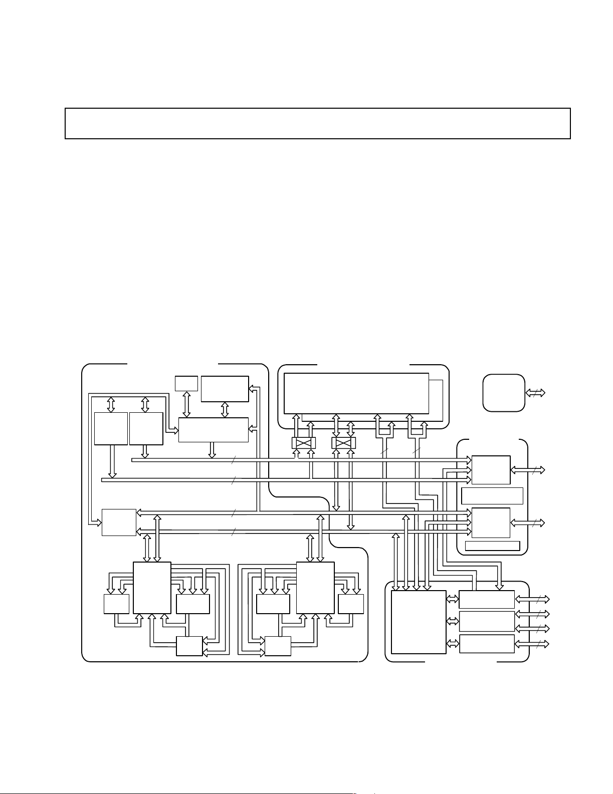
FUNCTIONAL BLOCK DIAGRAM
CORE PROCESSOR
INSTRUCTION
DAG1
8 4 32
DAG2
8 4 32
PM ADDRESS BUS
DM ADDRESS BUS
TIMER
CACHE
32 48- BIT
PROGRAM
SEQUENCER
PROCESSOR P ORT I/O PORT
ADDR DATA ADDR
32
32
Integrated Peripherals—Integrated I/O Processor,
4 M Bits On-Chip Dual-Ported SRAM, Glueless
Multiprocessing Features, and Ports (Serial, Link,
External Bus, and JTAG)
KEY FEATURES
100 MHz (10 ns) Core Instruction Rate
Single-Cycle Instruction Execution, Including SIMD
Operations in Both Computational Units
Dual Data Address Generators (DAGs) with Modulo and
Bit-Reverse Addressing
Zero-Overhead Looping and Single-Cycle Loop Setup,
Providing Efficient Program Sequencing
DUAL-PORTED SRAM
TWO INDEPENDENT
DUAL-PORTED BLOCKS
ADDR DATA
DATA
DATA
IOD
0
K
1
C
K
O
C
L
O
B
L
B
ADDR
IOA
64
18
JTAG
TEST AND
EMULATION
EXTERNAL
PORT
ADDR BUS
MUX
6
32
BUS
CONNECT
(PX)
MULT
PM DATA BUS
DM DATA BUS
DATA
REGISTER
FILE
(PEX)
16 40-BIT
BARREL
SHIFTER
ALU
16/32/40/48/64
32/40/64
BARREL
SHIFTER
ALU
REGISTER
16 40-BIT
SHARC and the SHARC logo are registered trademarks of Analog Devices, Inc.
REV. 0
Information furnished by Analog Devices is believed to be accurate and
reliable. However, no responsibility is assumed by Analog Devices for its
use, nor for any infringements of patents or other rights of third parties that
may result from its use. No license is granted by implication or otherwise
under any patent or patent rights of Analog Devices. Trademarks and
registered trademarks are the property of their respective companies.
MULTIPROCESSOR
INTERFACE
DATA BUS
MUX
HOST PORT
DATA
FILE
(PEY)
MULT
IOP
REGISTERS
(MEMORY
MAPPED)
CONTROL,
STATUS AND
DATA BUFFERS
I/O PROCESSOR
DMA
CONTROLLER
SERIAL PORTS
(2)
LINK PORTS
(6)
One Technology Way, P.O.Box 9106, Norwood, MA 02062-9106, U.S.A.
Tel:781/329-4700 www.analog.com
Fax:781/326-8703 © 2003 Analog Devices, Inc. All rights reserved.
64
4
6
6
60
Page 2

ADSP-21160N
KEY FEATURES (continued)
IEEE 1149.1 JTAG Standard Test Access Port and On-Chip
Emulation
400-Ball 27 mm 27 mm Metric PBGA Package
200 Million Fixed-Point MACs Sustained Performance
Single Instruction Multiple Data (SIMD)
Architecture Provides:
Two Computational Processing Elements
Concurrent Execution—Each Processing Element
Executes the Same Instruction, but Operates on
Different Data
Code Compatibility—at Assembly Level, Uses the
Same Instruction Set as the ADSP-2106x
SHARC DSPs
Parallelism in Buses and Computational Units Allows:
Single-Cycle Execution (with or without SIMD) of: A
Multiply Operation, An ALU Operation, A Dual
Memory Read or Write, and An Instruction Fetch
Transfers Between Memory and Core at up to Four
32-Bit Floating- or Fixed-Point Words per Cycle
Accelerated FFT Butterfly Computation Through a
Multiply with Add and Subtract
4M Bits On-Chip Dual-Ported SRAM for Independent
Access by Core Processor, Host, and DMA
DMA Controller Supports:
14 Zero-Overhead DMA Channels for Transfers Between
ADSP-21160N Internal Memory and External Memory,
External Peripherals, Host Processor, Serial Ports, or
Link Ports
64-Bit Background DMA Transfers at Core Clock Speed,
in Parallel with Full-Speed Processor Execution
Host Processor Interface to 16- and 32-Bit
Microprocessors
4G Word Address Range for Off-Chip Memory
Memory Interface Supports Programmable Wait State
Generation and Page-Mode for Off-Chip Memory
Multiprocessing Support Provides:
Glueless Connection for Scalable DSP Multiprocessing
Architecture
Distributed On-Chip Bus Arbitration for Parallel Bus
Connect of up to Six ADSP-21160Ns Plus Host
Six Link Ports for Point-to-Point Connectivity and Array
Multiprocessing
Serial Ports Provide:
Two 50M Bits/s Synchronous Serial Ports with
Companding Hardware
Independent Transmit and Receive Functions
TDM Support for T1 and E1 Interfaces
64-Bit Wide Synchronous External Port Provides:
Glueless Connection to Asynchronous and SBSRAM
External Memories
Up to 50 MHz Operation
–2– REV. 0
Page 3

ADSP-21160N
TABLE OF CONTENTS
GENERAL DESCRIPTION . . . . . . . . . . . . . . . . . . . . 4
ADSP-21160N Family Core Architecture . . . . . . . . . 4
SIMD Computational Engine . . . . . . . . . . . . . . . . 5
Independent, Parallel Computation Units . . . . . . . 5
Data Register File . . . . . . . . . . . . . . . . . . . . . . . . . 5
Single-Cycle Fetch of Instruction and
Four Operands . . . . . . . . . . . . . . . . . . . . . . . . . . 5
Instruction Cache . . . . . . . . . . . . . . . . . . . . . . . . . 5
Data Address Generators with Hardware
Circular Buffers . . . . . . . . . . . . . . . . . . . . . . . . . 5
Flexible Instruction Set . . . . . . . . . . . . . . . . . . . . . 5
ADSP-21160N Memory and I/O Interface Features . 5
Dual-Ported On-Chip Memory . . . . . . . . . . . . . . . 5
Off-Chip Memory and Peripherals Interface . . . . . 5
DMA Controller . . . . . . . . . . . . . . . . . . . . . . . . . . 6
Multiprocessing . . . . . . . . . . . . . . . . . . . . . . . . . . . 6
Link Ports . . . . . . . . . . . . . . . . . . . . . . . . . . . . . . . 8
Serial Ports . . . . . . . . . . . . . . . . . . . . . . . . . . . . . . 8
Host Processor Interface . . . . . . . . . . . . . . . . . . . . 8
Program Booting . . . . . . . . . . . . . . . . . . . . . . . . . . 8
Phase-Locked Loop . . . . . . . . . . . . . . . . . . . . . . . . 8
Power Supplies . . . . . . . . . . . . . . . . . . . . . . . . . . . 8
Development Tools . . . . . . . . . . . . . . . . . . . . . . . . . . 8
Designing an Emulator-Compatible
DSP Board (Target) . . . . . . . . . . . . . . . . . . . . . . . 9
Additional Information . . . . . . . . . . . . . . . . . . . . . . . 9
PIN FUNCTION DESCRIPTIONS . . . . . . . . . . . . . . 9
SPECIFICATIONS . . . . . . . . . . . . . . . . . . . . . . . . . . 14
ABSOLUTE MAXIMUM RATINGS . . . . . . . . . . 15
ESD SENSITIVITY . . . . . . . . . . . . . . . . . . . . . . . . 15
TIMING SPECIFICATIONS . . . . . . . . . . . . . . . . 16
Power-up Sequencing . . . . . . . . . . . . . . . . . . . . . 16
Clock Input . . . . . . . . . . . . . . . . . . . . . . . . . . . . . 18
Reset . . . . . . . . . . . . . . . . . . . . . . . . . . . . . . . . . . 18
Interrupts . . . . . . . . . . . . . . . . . . . . . . . . . . . . . . 19
Timer . . . . . . . . . . . . . . . . . . . . . . . . . . . . . . . . . 19
Flags . . . . . . . . . . . . . . . . . . . . . . . . . . . . . . . . . . 20
Memory Read—Bus Master . . . . . . . . . . . . . . . . 21
Memory Write—Bus Master . . . . . . . . . . . . . . . . 22
Synchronous Read/Write—Bus Master . . . . . . . . 23
Synchronous Read/Write—Bus Slave . . . . . . . . . 25
Multiprocessor Bus Request and
Host Bus Request . . . . . . . . . . . . . . . . . . . . . . 26
Asynchronous Read/Write—Host
to ADSP-21160N . . . . . . . . . . . . . . . . . . . . . . 28
Three-State Timing—Bus Master, Bus Slave . . . . 30
DMA Handshake . . . . . . . . . . . . . . . . . . . . . . . . 32
Link Ports —Receive, Transmit . . . . . . . . . . . . . . 34
Serial Ports . . . . . . . . . . . . . . . . . . . . . . . . . . . . . 36
JTAG Test Access Port and Emulation . . . . . . . . 39
Output Drive Currents . . . . . . . . . . . . . . . . . . . . . . 40
Power Dissipation . . . . . . . . . . . . . . . . . . . . . . . . . 40
Test Conditions . . . . . . . . . . . . . . . . . . . . . . . . . . . 41
Output Disable Time . . . . . . . . . . . . . . . . . . . . . 41
Output Enable Time . . . . . . . . . . . . . . . . . . . . . . 41
Example System Hold Time Calculation . . . . . . . 41
Capacitive Loading . . . . . . . . . . . . . . . . . . . . . . . 42
Environmental Conditions . . . . . . . . . . . . . . . . . . . 42
Thermal Characteristics . . . . . . . . . . . . . . . . . . . 42
400-BALL METRIC PBGA PIN
CONFIGURATIONS . . . . . . . . . . . . . . . . . . . . . . 43
OUTLINE DIMENSIONS . . . . . . . . . . . . . . . . . . . . 46
ORDERING GUIDE . . . . . . . . . . . . . . . . . . . . . . . . 46
–3–REV. 0
Page 4
ADSP-21160N
GENERAL DESCRIPTION
The ADSP-21160N SHARC DSP is the second iteration of the
ADSP-21160. Built in a 0.18 micron CMOS process, it offers
higher performance and lower power consumption than its predecessor, the ADSP-21160M. Easing portability, the ADSP21160N is application source code compatible with first generation ADSP-2106x SHARC DSPs in SISD (Single Instruction,
Single Data) mode. To take advantage of the processor’s SIMD
(Single Instruction, Multiple Data) capability, some code
changes are needed. Like other SHARCs, the ADSP-21160N is
a 32-bit processor that is optimized for high performance DSP
applications. The ADSP-21160N includes a 100 MHz core, a
dual-ported on-chip SRAM, an integrated I/O processor with
multiprocessing support, and multiple internal buses to eliminate
I/O bottlenecks.
The ADSP-21160N introduces Single-Instruction,
Multiple-Data (SIMD) processing. Using two computational
units (ADSP-2106x SHARC DSPs have one), the ADSP21160N can double performance versus the ADSP-2106x on a
range of DSP algorithms.
Fabricated in a state of the art, high speed, low power CMOS
process, the ADSP-21160N has a 10 ns instruction cycle time.
With its SIMD computational hardware running at 100 MHz,
the ADSP-21160N can perform 600 million math operations per
second.
Table 1 shows performance benchmarks for the ADSP-21160N.
Table 1. ADSP-21160N Benchmarks
Benchmark Algorithm Speed
1024 Point Complex FFT (Radix 4, with
171 µs
reversal)
FIR Filter (per tap) 5 ns
1
IIR Filter (per biquad) 40 ns
Matrix Multiply (pipelined)
[33] [31] 30 ns
[44] [41] 37 ns
Divide (y/x) 60 ns
Inverse Square Root 90 ns
1
1
DMA Transfer Rate 800M byte/s
1
Specified in SISD mode. Using SIMD, the same benchmark applies for
two sets of computations.For example, two sets of biquad operations can
be performed in the same amount of time as the SISD mode benchmark.
These benchmarks provide single-channel extrapolations of
measured dual-channel processing performance. For more information on benchmarking and optimizing DSP code for singleand dual-channel processing, see the Analog Devices website
(www.analog.com).
The ADSP-21160N continues SHARC’s industry-leading
standards of integration for DSPs, combining a high performance
32-bit DSP core with integrated, on-chip system features. These
features include a 4M-bit dual ported SRAM memory, host
processor interface, I/O processor that supports 14 DMA
channels, two serial ports, six link ports, external parallel bus,
and glueless multiprocessing.
The functional block diagram on Page 1 shows a block diagram
of the ADSP-21160N, illustrating the following architectural
features:
• Two processing elements, each made up of an AL U, M ul -
tiplier, Shifter, and Data Register File
• Data Address Generators (DAG1, DAG2)
• Program sequencer with instruction cache
• PM and DM buses capable of supporting four 32-bit data
transfers between memory and the core every core
processor cycle
• Interval timer
• On-Chip SRAM (4M bits)
• External port that supports:
• Interfacing to off-chip memory peripherals
• Glueless multiprocessing support for six ADSP-
21160N SHARCs
• Host port
• DMA controller
• Serial ports and link ports
• JTAG test access port
Figure 1 shows a typical single-processor system. A multiprocess-
ing system appears in Figure 4.
ADSP-21160
CLOCK
LINK
DEVICES
(6 MAX)
(OPTIONAL)
SERIAL
DEVICE
(OPTIONAL)
SERIAL
DEVICE
(OPTIONAL)
4
3
4
CLKIN
CLK_CFG3–0
EBOOT
LBOOT
IRQ2–0
FLAG3–0
TIMEXP
LXCLK
LXACK
LXDAT7–0
TCLK0
RCLK0
TFS0
RSF0
DT0
DR0
TCLK1
RCLK1
TFS1
RSF1
DT1
DR1
RPBA
ID2–0
RESET JTAG
BMS
CIF
BRST
ADDR31–0
DATA63–0
RDx
WRx
ACK
MS3–0
PAGE
SBTS
CLKOUT
DMAR1–2
DMAG1–2
CS
HBR
HBG
REDY
BR1–6
PA
6
CS
BOOT
EPROM
ADDR
(OPTIONAL)
DATA
ADDR
MEMORY/
DATA
MAPPED
OE
DEVICES
WE
(OPTIONAL)
ACK
L
O
R
T
N
O
C
CS
S
S
A
E
T
R
D
D
A
A
D
DMA DEVICE
DATA
PROCESSOR
INTERFACE
(OPTIONAL)
ADDR
DATA
(OPTIONAL)
HOST
Figure 1. Single-Processor System
ADSP-21160N Family Core Architecture
The ADSP-21160N includes the following architectural features
of the ADSP-2116x family core. The ADSP-21160N is code
compatible at the assembly level with the ADSP-2106x and
ADSP-21161.
–4– REV. 0
Page 5

ADSP-21160N
SIMD Computational Engine
The ADSP-21160N contains two computational processing
elements that operate as a Single Instruction Multiple Data
(SIMD) engine. The processing elements are referred to as PEX
and PEY, and each contains an ALU, multiplier, shifter, and
register file. PEX is always active, and PEY may be enabled by
setting the PEYEN mode bit in the MODE1 register. When this
mode is enabled, the same instruction is executed in both processing elements, but each processing element operates on
different data. This architecture is efficient at executing mathintensive DSP algorithms.
Entering SIMD mode also has an effect on the way data is transferred between memory and the processing elements. When in
SIMD mode, twice the data bandwidth is required to sustain
computational operation in the processing elements. Because of
this requirement, entering SIMD mode also doubles the
bandwidth between memory and the processing elements. When
using the DAGs to transfer data in SIMD mode, two data values
are transferred with each access of memory or the register file.
Independent, Parallel Computation Units
Within each processing element is a set of computational units.
The computational units consist of an arithmetic/logic unit
(ALU), multiplier, and shifter. These units perform single-cycle
instructions. The three units within each processing element are
arranged in parallel, maximizing computational throughput.
Single multifunction instructions execute parallel ALU and multiplier operations. In SIMD mode, the parallel ALU and
multiplier operations occur in both processing elements. These
computation units support IEEE 32-bit single-precision floatingpoint, 40-bit extended precision floating-point, and 32-bit fixedpoint data formats.
Data Register File
A general-purpose data register file is contained in each processing element. The register files transfer data between the
computation units and the data buses, and store intermediate
results. These 10-port, 32-register (16 primary, 16 secondary)
register files, combined with the ADSP-2116x enhanced Harvard
architecture, allow unconstrained data flow between computation units and internal memory. The registers in PEX are referred
to as R0–R15 and in PEY as S0–S15.
Single-Cycle Fetch of Instruction and Four Operands
The ADSP-21160N features an enhanced Harvard architecture
in which the data memory (DM) bus transfers data, and the
program memory (PM) bus transfers both instructions and data
(see the functional block diagram on Page 1). With the ADSP21160N’s separate program and data memory buses and on-chip
instruction cache, the processor can simultaneously fetch four
operands and an instruction (from the cache), all in a single cycle.
Instruction Cache
The ADSP-21160N includes an on-chip instruction cache that
enables three-bus operation for fetching an instruction and four
data values. The cache is selective—only the instructions whose
fetches conflict with PM bus data accesses are cached. This cache
allows full-speed execution of core, providing looped operations,
such as digital filter multiply- accumulates and FFT butterfly
processing.
Data Address Generators with Hardware
Circular Buffers
The ADSP-21160N’s two data address generators (DAGs) are
used for indirect addressing and provide for implementing
circular data buffers in hardware. Circular buffers allow efficient
programming of delay lines and other data structures required in
digital signal processing, and are commonly used in digital filters
and Fourier transforms. The two DAGs of the ADSP-21160N
contain sufficient registers to allow the creation of up to 32
circular buffers (16 primary register sets, 16 secondary). The
DAGs automatically handle address pointer wraparound,
reducing overhead, increasing performance, and simplifying
implementation. Circular buffers can start and end at any
memory location.
Flexible Instruction Set
The 48-bit instruction word accommodates a variety of parallel
operations, for concise programming. For example, the ADSP21160N can conditionally execute a multiply, an add, and
subtract, in both processing elements, while branching, all in a
single instruction.
ADSP-21160N Memory and I/O Interface Features
Augmenting the ADSP-2116x family core, the ADSP-21160N
adds the following architectural features:
Dual-Ported On-Chip Memory
The ADSP-21160N contains four megabits of on-chip SRAM,
organized as two blocks of 2M bits each, which can be configured
for different combinations of code and data storage. Each
memory block is dual-ported for single-cycle, independent
accesses by the core processor and I/O processor. The dualported memory in combination with three separate on-chip buses
allows two data transfers from the core and one from I/O processor, in a single cycle. On the ADSP-21160N, the memory can be
configured as a maximum of 128K words of 32-bit data, 256K
words of 16-bit data, 85K words of 48-bit instructions (or 40-bit
data), or combinations of different word sizes up to four megabits.
All of the memory can be accessed as 16-bit, 32-bit, 48-bit, or
64-bit words. A 16-bit floating-point storage format is supported
that effectively doubles the amount of data that may be stored
on-chip. Conversion between the 32-bit floating-point and 16bit floating-point formats is done in a single instruction. While
each memory block can store combinations of code and data,
accesses are most efficient when one block stores data, using the
DM bus for transfers, and the other block stores instructions and
data, using the PM bus for transfers. Using the DM bus and PM
bus in this way, with one dedicated to each memory block, assures
single-cycle execution with two data transfers. In this case, the
instruction must be available in the cache.
Off-Chip Memory and Peripherals Interface
The ADSP-21160N’s external port provides the processor’s
interface to off-chip memory and peripherals. The 4G word offchip address space is included in the ADSP-21160N’s unified
address space. The separate on-chip buses—for PM addresses,
–5–REV. 0
Page 6
ADSP-21160N
PM data, DM addresses, DM data, I/O addresses, and I/O data—
are multiplexed at the external port to create an external system
bus with a single 32-bit address bus and a single 64-bit data bus.
The lower 32 bits of the external data bus connect to even
addresses and the upper 32 bits of the 64 connect to odd
addresses. Every access to external memory is based on an
address that fetches a 32-bit word, and with the 64-bit bus, two
address locations can be accessed at once. When fetching an
instruction from external memory, two 32-bit data locations are
being accessed (16 bits are unused). Figure 3 shows the
alignment of various accesses to external memory.
The external port supports asynchronous, synchronous, and synchronous burst accesses. ZBT synchronous burst SRAM can be
interfaced gluelessly. Addressing of external memory devices is
facilitated by on-chip decoding of high order address lines to
generate memory bank select signals. Separate control lines are
also generated for simplified addressing of page-mode DRAM.
The ADSP-21160N provides programmable memory wait states
and external memory acknowledge controls to allow interfacing
to DRAM and peripherals with variable access, hold, and disable
time requirements.
Internal
Memory
Space
Multiprocessor
Memory
Space
IOP Reg’s
Long Word
Normal Word
Short Word
Internal
Memory
Space
(ID =001)
Internal
Memory
Space
(ID =010)
Internal
Memory
Space
(ID =011)
Internal
Memory
Space
(ID =100)
Internal
Memory
Space
(ID =101)
Internal
Memory
Space
(ID =110)
Broadcast
Write to
All DSPs
(ID =111)
0x00 0000
0x02 0000
0x04 0000
0x08 0000
0x10 0000
0x20 0000
0x30 0000
0x40 0000
0x50 0000
0x60 0000
0x70 0000
0x7F FFFF
Bank 0
Bank 1
Bank 2
Bank 3
Nonbanked
0x80 0000
MS
MS
MS
MS
External
Memory
Space
0xFFFF FFFF
0
1
2
3
Figure 2. Memory Map
DMA Controller
The ADSP-21160N’s on-chip DMA controller allows zerooverhead data transfers without processor intervention. The
DMA controller operates independently and invisibly to the
processor core, allowing DMA operations to occur while the core
is simultaneously executing its program instructions. DMA
transfers can occur between the ADSP-21160N’s internal
memory and external memory, external peripherals, or a host
processor. DMA transfers can also occur between the ADSP21160N’s internal memory and its serial ports or link ports.
External bus packing to 16-, 32-, 48-, or 64-bit words is
performed during DMA transfers. Fourteen channels of DMA
are available on the ADSP-21160N—six via the link ports, four
via the serial ports, and four via the processor’s external port (for
either host processor, other ADSP-21160Ns, memory or I/O
transfers). Programs can be downloaded to the ADSP-21160N
using DMA transfers. Asynchronous off-chip peripherals can
control two DMA channels using DMA Request/Grant lines
DMAR1–2, DMAG1–2
(
). Other DMA features include
interrupt generation upon completion of DMA transfers, twodimensional DMA, and DMA chaining for automatic linked
DMA transfers.
DATA63–0
63 55 47 39 31 23 15 7 0
BYTE 0BYTE 7
RDH/WRH
64-BIT LONG WORD, SIMD, DMA, IOP REGISTER TRANSFERS
64-BIT TRANSFER FOR 48-BIT INSTRUCTION FETCH
64-BIT TRANSFER FOR 40-BIT EXTENDED PRECISION
32-BIT NORMAL WORD (EVEN ADDRESS)
32-BIT NORMAL WORD (ODD ADDRESS)
RESTRICTED DMA, HOST, EPROM DATA ALIGNMENTS:
32-BIT PACKED
16-BIT PACKED
EPROM
RDL/WRL
Figure 3. External Data Alignment Options
Multiprocessing
The ADSP-21160N offers powerful features tailored to multiprocessing DSP systems as shown in Figure 4. The external port
and link ports provide integrated glueless multiprocessing
support.
The external port supports a unified address space (see Figure 2)
that allows direct interprocessor accesses of each ADSP21160N’s internal memory. Distributed bus arbitration logic is
included on-chip for simple, glueless connection of systems containing up to six ADSP-21160Ns and a host processor. Master
processor changeover incurs only one cycle of overhead. Bus
arbitration is selectable as either fixed or rotating priority. Bus
lock allows indivisible read-modify-write sequences for semaphores. A vector interrupt is provided for interprocessor
–6– REV. 0
Page 7
ADSP-21160N
commands. Maximum throughput for interprocessor data
transfer is 400M bytes/s over the external port. Broadcast writes
allow simultaneous transmission of data to all ADSP-21160Ns
and can be used to implement reflective semaphores.
ADSP-21160 #6
ADSP-21160 #5
ADSP-21160 #4
ADSP-21160 #3
ADDR31–0
CLKIN
DATA63–0
RESET
RPBA
3
ID2–0
CONTROL
011
PA
BR1–2, BR4–6
ADSP-21160 #2
CLKIN
RESET
RPBA
ADDR31–0
DATA63–0
5
BR3
Six link ports provide for a second method of multiprocessing
communications. Each link port can support communications to
another ADSP-21160N. Using the links, a large multiprocessor
system can be constructed in a 2D or 3D fashion. Systems can
use the link ports and cluster multiprocessing concurrently or
independently.
L
S
O
S
A
E
R
T
N
O
C
T
R
A
D
D
D
A
RESET
CLOCK
010
001
BUS
PRIORITY
3
3
ID2–0
BR1, BR3–6
ADSP-21160 #1
CLKIN
RESET
RPBA
ID2–0
CONTROL
PA
BR2
ADDR31–0
DATA63–0
RDx
WRx
ACK
L
MS3–0
O
R
T
N
O
BMS
C
PAGE
SBTS
CS
HBR
HBG
REDY
PA
BR2–6
BR1
5
L
S
S
O
R
T
N
O
C
5
A
E
T
R
A
D
D
D
A
ADDR
DATA
OE
WE
ACK
CS
CS
ADDR
DATA
ADDR
DATA
GLOBAL MEMORY
AND
PERIPHERAL (OPTIO NAL)
BOOT EPROM (OPTIONAL)
HOST PROCESSOR
INTERFACE (OPTIONAL)
Figure 4. Shared Memory Multiprocessing System
–7–REV. 0
Page 8
ADSP-21160N
Link Ports
The ADSP-21160N features six 8-bit link ports that provide
additional I/O capabilities. With the capability of running at
100 MHz rates, each link port can support 80M bytes/s. Link
port I/O is especially useful for point-to-point interprocessor
communication in multiprocessing systems. The link ports can
operate independently and simultaneously. Link port data is
packed into 48- or 32-bit words, and can be directly read by the
core processor or DMA-transferred to on-chip memory. Each
link port has its own double-buffered input and output registers.
Clock/acknowledge handshaking controls link port transfers.
Transfers are programmable as either transmit or receive.
Serial Ports
The ADSP-21160N features two synchronous serial ports that
provide an inexpensive interface to a wide variety of digital and
mixed-signal peripheral devices. The serial ports can operate up
to half the clock rate of the core, providing each with a maximum
data rate of 50M bit/s. Independent transmit and receive
functions provide greater flexibility for serial communications.
Serial port data can be automatically transferred to and from onchip memory via a dedicated DMA. Each of the serial ports offers
a TDM multichannel mode. The serial ports can operate with
little-endian or big-endian transmission formats, with word
lengths selectable from 3 bits to 32 bits. They offer selectable
synchronization and transmit modes as well as optional µ-law or
A-law companding. Serial port clocks and frame syncs can be
internally or externally generated.
Host Processor Interface
The ADSP-21160N host interface allows easy connection to
standard microprocessor buses, both 16-bit and 32-bit, with little
additional hardware required. The host interface is accessed
through the ADSP-21160N’s external port and is memorymapped into the unified address space. Four channels of DMA
are available for the host interface; code and data transfers are
accomplished with low software overhead. The host processor
communicates with the ADSP-21160N’s external bus with host
bus request (
), host bus grant (
HBG
), ready (REDY),
HBR
acknowledge (ACK), and chip select (CS) signals. The host can
directly read and write the internal memory of the ADSP21160N, and can access the DMA channel setup and mailbox
registers. Vector interrupt support provides efficient execution of
host commands.
Program Booting
The internal memory of the ADSP-21160N can be booted at
system power-up from an 8-bit EPROM, a host processor, or
through one of the link ports. Selection of the boot source is
BMS
controlled by the
(Boot Memory Select), EBOOT
(EPROM Boot), and LBOOT (Link/Host Boot) pins. 32-bit and
16-bit host processors can be used for booting.
Phase-Locked Loop
The ADSP-21160N uses an on-chip PLL to generate the internal
clock for the core. Ratios of 2:1, 3:1, and 4:1 between the core
and CLKIN are supported. The CLK_CFG pins are used to
select the ratio. The CLKIN rate is the rate at which the synchronous external port operates.
CROSSCORE is a trademark of Analog Devices, Inc.
VisualDSP++ is a registered trademark of Analog Devices, Inc.
Power Supplies
The ADSP-21160N has separate power supply connections for
the internal (V
), external (V
DDINT
), and analog (AVDD and
DDEXT
AGND) power supplies. The internal and analog supplies must
meet the 1.9 V requirement. The external supply must meet the
3.3 V requirement. All external supply pins must be connected
to the same supply.
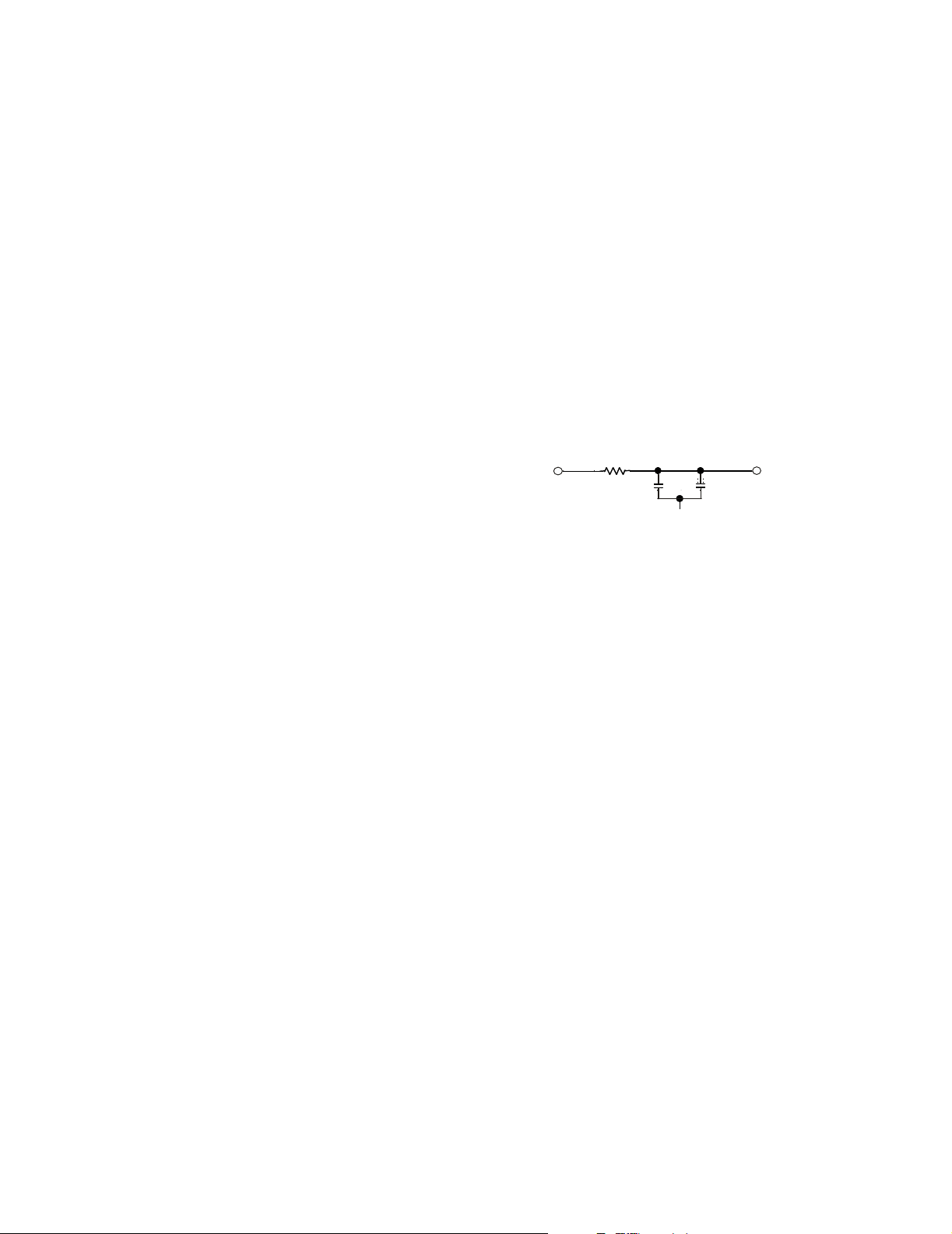
The PLL Filter, Figure 5, must be added for each ADSP21160N in the system. V
is the digital core supply. It is
DDINT
recommended that the capacitors be connected directly to
AGND using short thick trace. It is recommended that the capacitors be placed as close to AV
and AGND as possible. The
DD
connection from AGND to the (digital) ground plane should be
made after the capacitors. The use of a thick trace for AGND is
reasonable only because the PLL is a relatively low power
circuit—it does not apply to any other ADSP-21160N GND
connection.
V
DDINT
Figure 5. Analog Power (AVDD) Filter Circuit
Development Tools
10
0.1F
AGND
0.01F
AV
DD
The ADSP-21160N is supported with a complete set of
CROSSCORE™ software and hardware development tools,
including Analog Devices emulators and VisualDSP++
®
development environment. The same emulator hardware that
supports other ADSP-2116x processors also fully emulates the
ADSP-21160N.
The VisualDSP++ project management environment lets programmers develop and debug an application. This environment
includes an easy to use assembler (which is based on an algebraic
syntax), an archiver (librarian/library builder), a linker, a loader,
a cycle-accurate instruction-level simulator, a C/C++ compiler,
and a C/C++ runtime library that includes DSP and mathematical functions. A key point for these tools is C/C++ code
efficiency. The compiler has been developed for efficient translation of C/C++ code to DSP assembly. The DSP has architectural
features that improve the efficiency of compiled C/C++ code.
The VisualDSP++ debugger has a number of important features.
Data visualization is enhanced by a plotting package that offers
a significant level of flexibility. This graphical representation of
user data enables the programmer to quickly determine the performance of an algorithm. As algorithms grow in complexity, this
capability can have increasing significance on the designer’s
development schedule, increasing productivity. Statistical
profiling enables the programmer to nonintrusively poll the
processor as it is running the program. This feature, unique to
VisualDSP++, enables the software developer to passively gather
important code execution metrics without interrupting the realtime characteristics of the program. Essentially, the developer can
identify bottlenecks in software quickly and efficiently. By using
the profiler, the programmer can focus on those areas in the
program that impact performance and take corrective action.
–8– REV. 0
Page 9

ADSP-21160N
Debugging both C/C++ and assembly programs with the
VisualDSP++ debugger, programmers can:
• View mixed C/C++ and assembly code (interleaved
source and object information)
• Insert breakpoints
• Set conditional breakpoints on registers, memory,
and stacks
• Trace instruction execution
• Perform linear or statistical profiling of program
execution
• Fill, dump, and graphically plot the contents of memory
• Perform source level debugging
• Create custom debugger windows
The VisualDSP++ IDDE lets programmers define and manage
DSP software development. Its dialog boxes and property pages
let programmers configure and manage all of the ADSP-2116x
development tools, including the color syntax highlighting in the
VisualDSP++ editor. This capability permits programmers to:
• Control how the development tools process inputs and
generate outputs
• Maintain a one-to-one correspondence with the tool’s
command line switches
The VisualDSP++ Kernel (VDK) incorporates scheduling and
resource management tailored specifically to address the memory
and timing constraints of DSP programming. These capabilities
enable engineers to develop code more effectively, eliminating the
need to start from the very beginning, when developing new
application code. The VDK features include Threads, Critical
and Unscheduled regions, Semaphores, Events, and Device flags.
The VDK also supports Priority-based, Pre-emptive, Cooperative, and Time-Sliced scheduling approaches. In addition, the
VDK was designed to be scalable. If the application does not use
a specific feature, the support code for that feature is excluded
from the target system.
Because the VDK is a library, a developer can decide whether to
use it or not. The VDK is integrated into the VisualDSP++ development environment, but can also be used via standard
command line tools. When the VDK is used, the development
environment assists the developer with many error-prone tasks
and assists in managing system resources, automating the generation of various VDK based objects, and visualizing the system
state, when debugging an application that uses the VDK.
VCSE is Analog Devices technology for creating, using, and
reusing software components (independent modules of substantial functionality) to quickly and reliably assemble software
applications. Download components from the Web and drop
them into the application. Publish component archives from
within VisualDSP++. VCSE supports component implementation in C/C++ or assembly language.
Use the Expert Linker to visually manipulate the placement of
code and data on the embedded system. View memory utilization
in a color-coded graphical form, easily move code and data to
different areas of the DSP or external memory with the drag of
the mouse, examine run time stack and heap usage. The Expert
Linker is fully compatible with existing Linker Definition File
(LDF), allowing the developer to move between the graphical
and textual environments.
Analog Devices DSP emulators use the IEEE 1149.1 JTAG Test
Access Port of the ADSP-21160N processor to monitor and
control the target board processor during emulation. The
emulator provides full speed emulation, allowing inspection and
modification of memory, registers, and processor stacks. Nonintrusive in-circuit emulation is assured by the use of the processor’s
JTAG interface—the emulator does not affect target system
loading or timing.
In addition to the software and hardware development tools
available from Analog Devices, third parties provide a wide range
of tools supporting the ADSP-2116x processor family. Hardware
tools include ADSP-2116x processor PC plug-in cards. Third
party software tools include DSP libraries, real-time operating
systems, and block diagram design tools.
Designing an Emulator-Compatible DSP
Board (Target)
The Analog Devices family of emulators are tools that every DSP
developer needs to test and debug hardware and software
systems. Analog Devices has supplied an IEEE 1149.1 JTAG Test
Access Port (TAP) on each JTAG DSP. The emulator uses the
TAP to access the internal features of the DSP, allowing the
developer to load code, set breakpoints, observe variables,
observe memory, and examine registers. The DSP must be halted
to send data and commands, but once an operation has been
completed by the emulator, the DSP system is set running at full
speed with no impact on system timing.
To use these emulators, the target board must include a header
that connects the DSP’s JTAG port to the emulator.
For details on target board design issues including mechanical
layout, single processor connections, multiprocessor scan chains,
signal buffering, signal termination, and emulator pod logic, see
EE-68: Analog Devices JTAG Emulation Technical Reference
the
the Analog Devices website (www.analog.com)—use site search
on “EE-68.” This document is updated regularly to keep pace
with improvements to emulator support.
Additional Information
This data sheet provides a general overview of the ADSP-21160N
architecture and functionality. For detailed information on the
ADSP-2116x family core architecture and instruction set, refer
ADSP-21160 SHARC DSP Hardware Reference
to the
ADSP-21160 SHARC DSP Instruction Set Reference
information on the development tools for this processor, see the
VisualDSP++ User’s Guide for SHARC Processors
PIN FUNCTION DESCRIPTIONS
ADSP-21160N pin definitions are listed below. Inputs identified
as synchronous (S) must meet timing requirements with respect
to CLKIN (or with respect to TCK for TMS, TDI). Inputs
identified as asynchronous (A) can be asserted asynchronously
TRST
to CLKIN (or to TCK for
).
. For detailed
.
and the
on
–9–REV. 0
Page 10

ADSP-21160N
Tie or pull unused inputs to VDD or GND, except for the
following:
• ADDR31–0, DATA63–0, PAGE, BRST, CLKOUT
(ID2–0 = 00x) (Note: These pins have a logic-level hold
circuit enabled on the ADSP-21160N DSP with ID2–0
= 00x.)
• PA, ACK, MS3– 0, RDx, WRx, CIF, DMARx, DMAGx
(ID2–0 = 00x) (Note: These pins have a pull-up enabled
on the ADSP-21160N DSP with ID2–0 = 00x.)
Table 2. Pin Function Descriptions
Pin Type Function
ADDR31–0 I/O/T External Bus Address. The ADSP-21160N outputs addresses for external memory and
peripherals on these pins. In a multiprocessor system, the bus master outputs addresses
for read/writes of the internal memory or IOP registers of other ADSP-21160Ns. The
ADSP-21160N inputs addresses when a host processor or multiprocessing bus master
is reading or writing its internal memory or IOP registers. A keeper latch on the DSP’s
ADDR31–0 pins maintains the input at the level it was last driven (only enabled on the
ADSP-21160N with ID2–0 = 00x).
DATA63–0 I/O/T External Bus Data. The ADSP-21160N inputs and outputs data and instructions on
these pins. Pull-up resistors on unused DATA pins are not necessary. A keeper latch on
the DSP’s DATA63-0 pins maintains the input at the level it was last driven (only enabled
on the ADSP-21160N with ID2–0 = 00x).
MS3–0
RDL
RDH
WRL
WRH
O/T Memory Select Lines. These outputs are asserted (low) as chip selects for the corre-
s p on d i n g b a n ks o f e x t e r na l m em o r y. M em o r y b an k s iz e mu s t b e d e f i ne d i n t h e S Y S C ON
control register. The MS3–0 outputs are decoded memory address lines. In asynchronous access mode, the MS3–0 outputs transition with the other address outputs.
In synchronous access modes, the MS3–0 outputs assert with the other address lines;
however, they deassert after the first CLKIN cycle in which ACK is sampled asserted.
MS3–0 has a 20 kΩ internal pull-up resistor that is enabled on the ADSP-21160N with
ID2–0 = 00x.
I/O/T Memory Read Low Strobe. RDL is asserted whenever ADSP-21160N reads from the
low word of external memory or from the internal memory of other ADSP-21160Ns.
External devices, including other ADSP-21160Ns, must assert RDL for reading from
the low word of ADSP-21160N internal memory. In a multiprocessing system, RDL is
driven by the bus master. RDL has a 20 kΩ internal pull-up resistor that is enabled on
the ADSP-21160N with ID2–0 = 00x.
I/O/T Memory Read High Strobe. RDH is asserted whenever ADSP-21160N reads from the
high word of external memory or from the internal memory of other ADSP-21160Ns.
External devices, including other ADSP-21160Ns, must assert RDH for reading from
the high word of ADSP-21160N internal memory. In a multiprocessing system, RDH
is driven by the bus master. RDH has a 20 kΩ internal pull-up resistor that is enabled
on the ADSP-21160N with ID2–0 = 00x.
I/O/T Memory Write Low Strobe. WRL is asserted when ADSP-21160N writes to the low
word of external memory or inter nal memory of other ADSP-21160Ns. External devices
must assert WRL for writing to ADSP-21160N’s low word of internal memory. In a
multiprocessing system, WRL is driven by the bus master. WRL has a 20 kΩ internal
pull-up resistor that is enabled on the ADSP-21160N with ID2–0 = 00x.
I/O/T Memory Write High Strobe. WRH is asserted when ADSP-21160N writes to the high
word of external memory or inter nal memory of other ADSP-21160Ns. External devices
must assert WRH for writing to ADSP-21160N’s high word of internal memory. In a
multiprocessing system, WRH is driven by the bus master. WRH has a 20 kΩ internal
pull-up resistor that is enabled on the ADSP-21160N with ID2–0 = 00x.
• LxCLK, LxACK, LxDAT7–0 (LxPDRDE = 0) (Note:
See Link Port Buffer Control Register Bit definitions in
the ADSP-21160 DSP Hardware Reference.)
• DTx, DRx, TCLKx, RCLKx, EMU, TMS, TRST, TDI
(Note: These pins have a pull-up.)
The following symbols appear in the Type column of Table 2:
A = Asynchronous, G = Ground, I = Input, O = Output,
P=Power Supply, S=Synchronous, (A/D)=Active Drive,
SBTS
(O/D) = Open Drain, and T = Three-State (when
asserted, or when the ADSP-21160N is a bus slave).
is
–10– REV. 0
Page 11

ADSP-21160N
Table 2. Pin Function Descriptions (continued)
Pin Type Function
PAGE O/T DRAM Page Boundary. The ADSP-21160N asserts this pin to an external DRAM
controller, to signal that an external DRAM page boundary has been crossed. DRAM
page size must be defined in the ADSP-21160N’s memory control register (WAIT).
DRAM can only be implemented in ext er na l mem or y Ba nk 0 ; the PAGE si gna l can only
be activated for Bank 0 accesses. In a multiprocessing system PAGE is output by the
bus master. A keeper latch on the DSP’s PAGE pin maintains the output at the level it
was last driven (only enabled on the ADSP-21160N with ID2–0 = 00x).
BRST I/O/T Sequential Burst Access. BRST is asserted by ADSP-21160N or a host to indicate that
data associated with consecutive addresses is being read or written. A slave device
samples the initial address and increments an internal address counter after each
transfer. The incremented address is not pipelined on the bus. If the burst access is a
read from host to ADSP-21160N, ADSP-21160N automatically increments the address
as long as BRST is asserted. BRST is asserted after the initial access of a burst transfer.
It is asserted for every cycle after that, except for the last data request cycle (denoted by
RDx or WRx asserted and BRST negated). A keeper latch on the DSP’s BRST pin
maintains the input at the level it was last driven (only enabled on the ADSP-21160N
with ID2–0 = 00x).
ACK I/O/S Memory Acknowledge. External devices can deassert ACK (low) to add wait states to
an external memory access. ACK is used by I/O devices, memory controllers, or other
peripherals to hold off completion of an external memory access. The ADSP-21160N
deasserts ACK as an output to add wait states to a synchronous access of its internal
memory, by a synchronous host or another DSP in a multiprocessor configuration. ACK
has a 2 kΩ internal pull-up resistor that is enabled on the ADSP-21160N with
ID2–0 = 00x.
SBTS
IRQ2–0
FLAG3–0 I/O/A Flag Pins. Each is configured via control bits as either an input or output. As an input,
TIMEXP O Timer Expired. Asserted for four Core Clock cycles when the timer is enabled and
HBR
HBG
CS
REDY O (O/D) Host Bus Acknowledge. The ADSP-21160N deasserts REDY (low) to add wait states
DMAR1
I/S Suspend Bus and Three-State. External devices can assert SBTS (low) to place the
external bus address, data, selects, and strobes in a high impedance state for the following
cycle. If the ADSP-21160N attempts to access external memory while SBTS is asserted,
the processor will halt and the memory access will not be completed until SBTS is
deasserted. SBTS should only be used to recover from host processor and/or ADSP21160N deadlock or used with a DRAM controller.
I/A Interrupt Request Lines. These are sampled on the rising edge of CLKIN and may be
either edge-triggered or level-sensitive.
it can be tested as a condition. As an out put, it ca n be u sed to si gnal ext er nal p er iph eral s.
TCOUNT decrements to zero.
I/A Host Bus Request. Must be asserted by a host processor to request control of the ADSP-
21160N’s external bus. When HBR is asserted in a multiprocessing system, the ADSP21160N that is bus master will relinquish the bus and assert HBG. To relinquish the
bus, the ADSP-21160N places the address, data, select, and strobe lines in a high
impedance state. HBR has priority over all ADSP-21160N bus requests (BR6–1) in a
multiprocessing system.
I/O Host Bus Grant. Acknowledges an HBR bus request, indicating that the host processor
may take control of the external bus. HBG is asserted (held low) by the ADSP-21160N
until HBR is released. In a multiprocessing system, HBG is output by the ADSP21160N bus master and is monitored by all others. After HBR is asserted, and before
HBG is given, HBG will float for 1 t
HBG should be pulled up with a 20 kΩ to 50 kΩ external resistor.
I/A Chip Select. Asserted by host processor to select the ADSP-21160N, for asynchronous
transfer protocol.
to an asynchronous host access when CS and HBR inputs are asserted.
I/A DMA Request 1 (DMA Channel 11). Asserted by external port devices to request DMA
services. DMAR1 has a 20 kΩ internal pull-up resistor that is enabled on the ADSP21160N with ID2–0 = 00x.
(1 CLKIN cycle). To avoid erroneous grants,
CLK
–11–REV. 0
Page 12

ADSP-21160N
Table 2. Pin Function Descriptions (continued)
Pin Type Function
DMAR2 I/A DMA Request 2 (DMA Channel 12). Asserted by external port devices to request DMA
services. DMAR2 has a 20 kΩ internal pull-up resistor that is enabled on the ADSP21160N with ID2–0 = 00x.
ID2–0 I Multiprocessing ID. Determines which multiprocessing bus request (BR1–BR6) is used
by ADSP-21160N. ID = 001 corresponds to BR1, ID = 010 corresponds to BR2, and
so on. Use ID = 000 or ID = 001 in single-processor systems. These lines are a system
configuration selection which should be hardwired or only changed at reset.
DMAG1 O/T DMA Grant 1 (DMA Channel 11). Asserted by ADSP-21160N to indicate that the
requested DMA starts on the next cycle. Driven by bus master only. DMAG1 has a
20 kΩ internal pull-up resistor that is enabled on the ADSP-21160N with ID2–0 = 00x.
DMAG2 O/T DMA Grant 2 (DMA Channel 12). Asserted by ADSP-21160N to indicate that the
requested DMA starts on the next cycle. Driven by bus master only. DMAG2 has a
20 kΩ internal pull-up resistor that is enabled on the ADSP-21160N with ID2–0 = 00x.
BR6–1
RPBA I/S Rotating Priority Bus Arbitration Select. When RPBA is high, rotating priority for
PA
DTx O Data Transmit (Serial Ports 0, 1). Each DT pin has a 50 kΩ internal pull-up resistor.
DRx I Data Receive (Serial Ports 0, 1). Each DR pin has a 50 kΩ internal pull-up resistor.
TCLKx I/O Transmit Clock (Serial Ports 0, 1). Each TCLK pin has a 50 kΩ internal pull-up resistor.
RCLKx I/O Receive Clock (Serial Ports 0, 1). Each RCLK pin has a 50 kΩ internal pull-up resistor.
TFSx I/O Transmit Frame Sync (Serial Ports 0, 1).
RFSx I/O Receive Frame Sync (Serial Ports 0, 1).
LxDAT7–0 I/O Link Port Data (Link Ports 0–5). Each LxDAT pin has a 50 kΩ internal pull-down
LxCLK I/O Link Port Clock (Link Ports 0–5). Each LxCLK pin has a 50 kΩ internal pull-down
LxACK I/O Link Port Acknowledge (Link Ports 0–5). Each LxACK pin has a 50 kΩ internal pull-
EBOOT I EPROM Boot Select. For a description of how this pin operates, see Table 3. This signal
LBOOT I Link Boot. For a description of how this pin operates, see Table 3. This signal is a system
BMS
CLKIN I Local Clock In. CLKIN is the ADSP-21160N clock input. The ADSP-21160N external
I/O/S Multiprocessing Bus Requests. Used by multiprocessing ADSP-21160Ns to arbitrate
for bus mastership. An ADSP-21160N only drives its own BRx line (corresponding to
the value of its ID2–0 inputs) and monitors all others. In a multiprocessor system with
less than six ADSP-21160Ns, the unused BRx pins should be pulled high; the processor’s
own BRx line must not be pulled high or low because it is an output.
multiprocessor bus arbitration is selected. When RPBA is low, fixed priority is selected.
This signal is a system configuration selection which must be set to the same value on
every ADSP-21160N. If the value of RPBA is changed during system operation, it must
be changed in the same CLKIN cycle on every ADSP-21160N.
I/O/T Priority Access. Asserting its PA pin allows an ADSP-21160N bus slave to interrupt
background DMA transfers and gain access to the external bus. PA is connected to all
ADSP-21160Ns in the system. If access priority is not required in a system, the PA pin
should be left unconnected. PA has a 20 kΩ internal pull-up resistor that is enabled on
the ADSP-21160N with ID2–0 = 00x.
resistor that is enabled or disabled by the LPDRD bit of the LCTL0–1 register.
resistor that is enabled or disabled by the LPDRD bit of the LCTL0–1 register.
down resistor that is enabled or disabled by the LPDRD bit of the LCOM register.
is a system configuration selection that should be hardwired.
configuration selection that should be hardwired.
I/O/T Boot Memory Select. Serves as an output or input as selected with the EBOOT and
LBOOT pins; see Table 3. This input is a system configuration selection that should be
hardwired.
port cycles at the frequency of CLKIN. The instruction cycle rate is a multiple of the
CLKIN frequency; it is programmable at power-up. CLKIN may not be halted,
changed, or operated below the specified frequency.
–12– REV. 0
Page 13
ADSP-21160N
Table 2. Pin Function Descriptions (continued)
Pin Type Function
CLK_CFG3–0 I Core/CLKIN Ratio Control. ADSP-21160N core clock (instruction cycle) rate is equal
to n CLKIN where n is user-selectable to 2, 3, or 4, using the CLK_CFG3–0 inputs.
For clock configuration definitions, see the RESET & CLKIN section of the System
Design chapter of the ADSP-21160 SHARC DSP Hardware Reference manual.
CLKOUT O/T CLKOUT is driven at the CLKIN frequency by the ADSP-21160N. This output can
be three-stated by setting the COD bit in the SYSCON register. A keeper latch on the
DSP’s CLKOUT pin maintains the output at the level it was last driven (only enabled
on the ADSP-21160N with ID2-0 = 00x). Do not use CLKOUT in multiprocessing
systems; use CLKIN instead.
RESET
TCK I Test Clock (JTAG). Provides a clock for JTAG boundary scan.
TMS I/S Test Mode Select (JTAG). Used to control the test state machine. TMS has a 20 kΩ
TDI I/S Test Data Input (JTAG). Provides serial data for the boundary scan logic. TDI has a
TDO O Test Data Output (JTAG). Serial scan output of the boundary scan path.
TRST
EMU
CIF
V
DDINT
V
DDEXT
AV
DD
AGND G Analog Power Supply Return.
GND G Power Supply Return (82 pins).
NC Do Not Connect. Reserved pins that must be left open and unconnected (9 pins).
I/A Processor Reset. Resets the ADSP-21160N to a known state and begins execution at
the program memory location specified by the hardware reset vector address. The
RESET input must be asserted (low) at power-up.
internal pull-up resistor.
20 kΩ internal pull-up resistor.
I/A Test Reset (JTAG). Resets the test state machine. TRST must be asserted (pulsed low)
after power-up or held low for proper operation of the ADSP-21160N. TRST has a
20 kΩ internal pull-up resistor.
O (O/D) Emulation Status. Must be connected to the ADSP-21160N emulator target board
connector only. EMU has a 50 kΩ internal pull-up resistor.
O/T Core Instruction Fetch. Signal is active low when an external instruction fetch is
performed. Driven by bus master only. Three-state when host is bus master. CIF has a
20 kΩ internal pull-up resistor that is enabled on the ADSP-21160N with ID2–0 = 00x.
P Core Power Supply. Nominally 1.9 V dc and supplies the DSP’s core processor
(40 pins).
P I/O Power Supply. Nominally 3.3 V dc (43 pins).
P Analog Power Supply. Nominally 1.9 V dc and supplies the DSP’s internal PLL (clock
generator). This pin has the same specifications as V
, except that added filtering
DDINT
circuitry is required. For more information, see Power Supplies on Page 8.
Table 3. Boot Mode Selection
EBOOT LBOOT BMS Booting Mode
1 0 Output EPROM (Connect BMS to EPROM chip select.)
0 0 1 (Input) Host Processor
0 1 1 (Input) Link Port
0 0 0 (Input) No Booting. Processor executes from external memory.
0 1 0 (Input) Reserved
1 1 x (Input) Reserved
–13–REV. 0
Page 14

ADSP-21160N
SPECIFICATIONS
RECOMMENDED OPERATING CONDITIONS
C Grade K Grade
UnitParameter Min Max Min Max
V
DDINT
AV
DD
V
DDEXT
T
CASE
V
IH1
V
IH2
V
IL
Specifications subject to change without notice.
1
See Environmental Conditions on Page 42 for information on thermal specifications.
2
Applies to input and bidirectional pins: DATA63–0, ADDR31–0, RDx, WRx, ACK, SBTS, IRQ2–0, FLAG3–0, HBG, CS, DMAR1, DMAR2, BR6–1,
ID2–0, RPBA, PA, BRST, TFS0, TFS1, RFS0, RFS1, LxDAT3–0, LxCLK, LxACK, EBOOT, LBOOT, BMS, TMS, TDI, TCK, HBR, DR0, DR1,
TCLK0, TCLK1, RCLK0, RCLK1.
3
Applies to input pins: CLKIN, RESET, TRST.
ELECTRICAL CHARACTERISTICS
Internal (Core) Supply Voltage 1.8 2.0 1.8 2.0 V
Analog (PLL) Supply Voltage 1.8 2.0 1.8 2.0 V
External (I/O) Supply Voltage 3.13 3.47 3.13 3.47 V
2, 3
1
@ V
– 40 +100 0 85 ºC
=Max
DDEXT
=Max
DDEXT
=Min –0.5 +0.8 –0.5 +0.8 V
DDEXT
2.0 V
2.0 V
+0.5 2.0 V
DDEXT
+0.5 2.0 V
DDEXT
DDEXT
DDEXT
+0.5 V
+0.5 V
Case Operating Temperature
High Level Input Voltage,2 @ V
High Level Input Voltage,3 @ V
Low Level Input Voltage,
Parameter Test Conditions Min Max Unit
V
OH
V
OL
I
IH
I
IL
I
IHC
I
ILC
I
IKH
I
IKL
I
IKH-OD
I
IKL-OD
I
ILPU1
I
ILPU2
I
OZH
I
OZL
I
OZHPD
I
OZLPU1
I
OZLPU2
I
OZHA
I
OZLA
I
DD-INPEAK
I
DD-INHIGH
I
DD-INLOW
I
DD-IDLE
AI
DD
C
IN
Specifications subject to change without notice.
1
Applies to output and bidirectional pins: DATA63–0, ADDR31–0, MS3–0, RDx, WRx, PAGE, CLKOUT, ACK, FLAG3–0, TIMEXP, HBG, REDY,
DMAG1, DMAG2, BR6–1, PA, BRST, CIF, DT0, DT1, TCLK0, TCLK1, RCLK0, RCLK1, TFS0, TFS1, RFS0, RFS1, LxDAT3–0, LxCLK, LxACK,
BMS, TDO, EMU.
2
See Output Drive Currents on Page 40 for typical drive current capabilities.
3
Applies to input pins: SBTS, IRQ2–0, HBR, CS, ID2–0, RPBA, EBOOT, LBOOT, CLKIN, RESET, TCK, CLK_CFG3-0.
4
Applies to input pins with internal pull-ups: DR0, DR1.
5
Applies to input pins with internal pull-ups: DMARx, TMS, TDI, TRST.
High Level Output Voltage
Low Level Output Voltage
High Level Input Current
Low Level Input Current
CLKIN High Level Input Current
CLKIN Low Level Input Current
Keeper High Load Current
Keeper Low Load Current
Keeper High Overdrive Current7, 8,
Keeper Low Overdrive Current7, 8,
Low Level Input Current Pull-Up1
Low Level Input Current Pull-Up2
Three-State Leakage Current
Three-State Leakage Current
Three-State Leakage Current Pull-Down13@ V
Three-State Leakage Current Pull-Up1
Three-State Leakage Current Pull-Up2
Three-State Leakage Current
Three-State Leakage Current
Supply Current (Internal)
Supply Current (Internal)
Supply Current (Internal)
Supply Current (Idle)
Supply Current (Analog)
Input Capacitance
19, 20
1
1
3, 4, 5
3
6
6
7
7
9
9
4
5
10, 11, 12, 13
10
14
14
15
16
17
18
6
@ V
@ V
@ V
@ V
@ V
@ V
@ V
@ V
@ V
@ V
@ V
@ V
@ V
@ V
11
@ V
12
@ V
@ V
@ V
t
CCLK
t
CCLK
t
CCLK
t
CCLK
=Min, IOH=–2.0 mA
DDEXT
=Min, IOL=4.0 mA
DDEXT
=Max, VIN=VDD Max 10 µA
DDEXT
=Max, VIN=0 V 10 µA
DDEXT
= Max, VIN = V
DDEXT
= Max, VIN = 0 V 25 µA
DDEXT
= Max, VIN = 2.0 V –250 –50 µA
DDEXT
= Max, VIN = 0.8 V 50 200 µA
DDEXT
= Max –300 µA
DDEXT
= Max 300 µA
DDEXT
=Max, VIN=0 V 250 µA
DDEXT
=Max, VIN=0 V 500 µA
DDEXT
=Max, VIN=VDD Max 10 µA
DDEXT
=Max, VIN=0 V 10 µA
DDEXT
=Max, VIN=V
DDEXT
=Max, VIN=0 V 250 µA
DDEXT
=Max, VIN=0 V 500 µA
DDEXT
=Max, VIN=V
DDEXT
=Max, VIN=0 V 4 mA
DDEXT
=10.0 ns, V
=10.0 ns, V
=10.0 ns, V
=10.0 ns, V
=Max 960 mA
DDINT
=Max 715 mA
DDINT
=Max 550 mA
DDINT
=Max 450 mA
DDINT
@AVDD=Max 10 mA
fIN=1 MHz, T
=25°C, VIN=2.5 V 4.7 pF
CASE
2
2
Max 25 µA
DDEXT
Max 250 µA
DD
Max 25 µA
DD
2.4 V
0.4 V
–14– REV. 0
Page 15

ADSP-21160N
6
Applies to CLKIN only.
7
Applies to all pins with keeper latches: ADDR31–0, DATA63–0, PAGE, BRST, CLKOUT.
8
Current required to switch from kept high to low or from kept low to high.
9
Characterized, but not tested.
10
Applies to three-statable pins: DATA63–0, ADDR31–0, PAGE, CLKOUT, ACK, FLAG3–0, REDY, HBG, BMS, BR6–1, TFSx, RFSx, TDO.
11
Applies to three-statable pins with internal pull-ups: DTx, TCLKx, RCLKx, EMU.
12
Applies to three-statable pins with internal pull-ups: MS3–0, RDx, WRx, DMAGx, PA, CIF.
13
Applies to three-statable pins with internal pull-downs: LxDAT7–0, LxCLK, LxACK.
14
Applies to ACK pulled up internally with 2 kΩ during reset or ID2–0 = 00x.
15
The test program used to measure I
internal power measurements made using typical applications are less than specified. For more information, see Power Dissipation on Page 40.
16
I
DD-INHIGH
17
I
DD-INLOW
18
Idle denotes ADSP-21160N state during execution of IDLE instruction. For more information, see Power Dissipation on Page 40.
19
Applies to all signal pins.
20
Guaranteed, but not tested.
is a composite average based on a range of high activity code. For more information, see Power Dissipation on Page 40.
is a composite average based on a range of low activity code. For more information, see Power Dissipation on Page 40.
DD-INPEAK
ABSOLUTE MAXIMUM RATINGS
Internal (Core) Supply Voltage (V
Analog (PLL) Supply Voltage (AVDD)1. . . . –0.3 V to +2.3 V
External (I/O) Supply Voltage (V
1
Input Voltage
Output Voltage Swing
Load Capacitance
Storage Temperature Range
1
Stresses greater than those listed above may cause permanent damage to the
device. These are stress ratings only; functional operation of the device at these
or any other conditions greater than those indicated in the operational sections
of this specification is not implied. Exposure to absolute maximum rating con ditions for extended periods may affect device reliability.
. . . . . . . . . . . . . . . . –0.5 V to V
1
. . . . . . . . . –0.5 V to V
1
. . . . . . . . . . . . . . . . . . . . . . . . . .200 pF
1
represents worst-case processor operation and is not sustainable under normal application conditions. Actual
)1. . –0.3 V to +2.3 V
DDINT
)1 . . –0.3 V to +4.6 V
DDEXT
+ 0.5 V
DDEXT
+ 0.5 V
DDEXT
. . . . . . . . . . .–65°C to +150°C
ESD SENSITIVITY
CAUTION
ESD (electrostatic discharge) sensitive device. Electrostatic charges as high as 4000 V
readily accumulate on the human body and test equipment and can discharge without
detection. Although the ADSP-21160N features proprietary ESD protection circuitry,
permanent damage may occur on devices subjected to high energy electrostatic
discharges. Therefore, proper ESD precautions are recommended to avoid performance
degradation or loss of functionality.
–15–REV. 0
Page 16

ADSP-21160N
TIMING SPECIFICATIONS
The ADSP-21160N’s internal clock switches at higher frequencies than the system input clock (CLKIN). To generate the
internal clock, the DSP uses an internal phase-locked loop
(PLL). This PLL-based clocking minimizes the skew between
the system clock (CLKIN) signal and the DSP’s internal clock
(the clock source for the external port logic and I/O pads).
The ADSP-21160N’s internal clock (a multiple of CLKIN)
provides the clock signal for timing internal memory, processor
core, link ports, serial ports, and external port (as required for
read/write strobes in asynchronous access mode). During reset,
program the ratio between the DSP’s internal clock frequency
and external (CLKIN) clock frequency with the CLK_CFG3–0
pins. Even though the internal clock is the clock source for the
external port, the external port clock always switches at the
CLKIN frequency. To determine switching frequencies for the
serial and link ports, divide down the internal clock, using the
programmable divider control of each port (TDIVx/RDIVx for
the serial ports and LxCLKD1–0 for the link ports).
Note the following definitions of various clock periods that are a
function of CLKIN and the appropriate ratio control:
• t
= (tCK) / CR
CCLK
• t
• t
LCLK
SCLK
= (t
= (t
CCLK
CCLK
) LR
) SR
where:
• LCLK = Link Port Clock
• SCLK = Serial Port Clock
• t
= CLKIN Clock Period
CK
• t
= (Processor) Core Clock Period
CCLK
• t
= Link Port Clock Period
LCLK
• t
= Serial Port Clock Period
SCLK
• CR = Core/CLKIN Ratio (2, 3, or 4:1,
determined by CLK_CFG3–0 at reset)
• LR = Link Port/Core Clock Ratio (1, 2, 3, or 4:1,
determined by LxCLKD)
• SR = Serial Port/Core Clock Ratio (wide range,
determined by CLKDIV)
Use the exact timing information given. Do not attempt to derive
parameters from the addition or subtraction of others. While
addition or subtraction would yield meaningful results for an
individual device, the values given in this data sheet reflect statistical variations and worst cases. Consequently, it is not
meaningful to add parameters to derive longer times.
See Figure 30 on Page 41 under Test Conditions for voltage
reference levels.
Switching Characteristics specify how the processor changes its
signals. Circuitry external to the processor must be designed for
compatibility with these signal characteristics. Switching characteristics describe what the processor will do in a given
circumstance. Use switching characteristics to ensure that any
timing requirement of a device connected to the processor (such
as memory) is satisfied.
Timing Requirements apply to signals that are controlled by
circuitry external to the processor, such as the data input for a
read operation. Timing requirements guarantee that the
processor operates correctly with other devices.
During processor reset (
RESET
bit in SYSCON register = 1), deassertion (
DMAGx, RDx, WRx, CIF
(FLAG3-0, LxCLK, LxACK, LxDAT7-0, ACK, REDY,
TFSx, RFSx, TCLKx, RCLKx, DTx,
pin low) or software reset (SRST
MS3–0, HBG
,
, PAGE, BRST) and three-state
BMS
, TDO,
EMU
PA
,
,
DATA) timings differ. These occur asynchronously to CLKIN,
and may not meet the specifications published in the Timing
Requirements and Switching Characteristics tables. The
maximum delay for deassertion and three-state is one t
RESET
During reset the DSP will not respond to
accesses.
HBG
pin assertion low or setting the SRST bit in SYSCON.
SBTS, HBR
HBR
asserted before reset will be recognized, but a
will not be returned by the DSP until after reset is
from
CK
and MMS
deasserted and the DSP has completed bus synchronization.
Power-up Sequencing
For power-up sequencing, see Table 4 and Figure 6. During the
power-up sequence of the DSP, differences in the ramp-up rates
and activation time between the two power supplies can cause
current to flow in the I/O ESD protection circuitry. To prevent
this damage to the ESD diode protection circuitry, Analog
Devices, Inc. recommends including a bootstrap Schottky diode
(see Figure 7). The bootstrap Schottky diode connected between
the 1.9 V and 3.3 V power supplies protects the ADSP-21160N
from partially powering the 3.3 V supply. Including a Schottky
diode will shorten the delay between the supply ramps and thus
prevent damage to the ESD diode protection circuitry. With this
technique, if the 1.9 V rail rises ahead of the 3.3 V rail, the
Schottky diode pulls the 3.3 V rail along with the 1.9 V rail.
–16– REV. 0
Page 17

ADSP-21160N
Table 4. Power-up Sequencing
Parameter Min Max Unit
Timing Requirements
t
RSTVDD
t
IVDDEVDD
t
CLKVDD
t
CLKRST
t
PLLRST
RESET Low Before V
V
on Before V
DDINT
DDINT/VDDEXT
DDEXT
CLKIN Running After valid V
on 0 ns
– 50 +200 ms
DDINT/VDDEXT
1
0 200 ms
CLKIN Valid Before RESET Deasserted 10
PLL Control Setup Before RESET Deasserted 20
2
3
µs
µs
Switching Characteristics
t
CORERST
1
Valid V
DDINT/VDDEXT
of milliseconds, depending on the design of the power supply subsystem.
2
Assumes a stable CLKIN signal after meeting worst-case start-up timing of oscillators. Refer to your oscillator manufacturer’s data sheet for start-up time.
3
Based on CLKIN cycles.
4
CORERST is an internal signal only. The 4096 cycle count is dependent on t
DSP Core Reset Deasserted After RESET Deasserted 4096t
assumes that the supplies are fully ramped to their 1.9 V and 3.3 V rails. Voltage ramp rates can vary from microseconds to hundreds
specification. If setup time is not met, one additional CLKIN cycle may
SRST
be added to the core reset time, resulting in 4097 cycles maximum.
RESET
t
RSTVDD
V
DDINT
V
DDEXT
CLKIN
t
IVDDEVDD
t
CLKVDD
t
CLKRST
CK
3, 4
ms
CLK_CFG3-0
CORERST
t
PLLRST
Figure 6. Power-up Sequencing
3.3V I/O
VOLTAGE REGULATOR
1.9V CORE
VOLTAGE REGULATOR
Figure 7. Dual Voltage Schottky Diode
–17–REV. 0
t
CORERST
V
DDEXT
ADSP-21160
V
DDINT
Page 18

ADSP-21160N
Clock Input
For Clock Input, see Table 5 and Figure 8.
Table 5. Clock Input
Parameter
Timing Requirements
t
CK
t
CKL
t
CKH
t
CKRF
t
CCLK
CLKIN Period 20 80 ns
CLKIN Width Low 7.5 40 ns
CLKIN Width High 7.5 40 ns
CLKIN Rise/Fall (0.4 V–2.0 V) 3 ns
Core Clock Period 10 30 ns
CLKIN
t
CKH
Figure 8. Clock Input
100 MHz
UnitMin Max
t
CK
t
CKL
Reset
For Reset, see Table 6 and Figure 9.
Table 6. Reset
Parameter Min Max Unit
Timing Requirements
t
WRST
t
SRST
1
Applies after the power-up sequence is complete. At power-up, the processor’s internal phase-locked loop requires no more than 100 µs while RESET is
low, assuming stable VDD and CLKIN (not including start-up time of external clock oscillator).
2
Only required if multiple ADSP-21160Ns must come out of reset synchronous to CLKIN with program counters (PC) equal. Not required for multiple
ADSP-21160Ns communicating over the shared bus (through the external port), because the bus arbitration logic automatically synchronizes itself
after reset.
RESET Pulsewidth Low
RESET Setup Before CLKIN High
CLKIN
RESET
1
2
t
WRST
4t
CK
ns
8ns
t
SRST
Figure 9. Reset
–18– REV. 0
Page 19

ADSP-21160N
Interrupts
For Interrupts, see Table 7 and Figure 10.
Table 7. Interrupts
Parameter Min Max Unit
Timing Requirements
t
SIR
t
HIR
t
IPW
1
Only required for IRQx recognition in the following cycle.
2
Applies only if t
IRQ2–0 Setup Before CLKIN High
IRQ2–0 Hold After CLKIN High
IRQ2–0 Pulsewidth
SIR
and t
requirements are not met.
HIR
2
CLKIN
IRQ2–0
1
1
t
SIR
t
IPW
Figure 10. Interrupts
6ns
0ns
2+t
t
HIR
CK
ns
Timer
For Timer, see Table 8 and Figure 11.
Table 8. Timer
Parameter Min Max Unit
Switching Characteristic
t
DTEX
CLKIN
TIMEXP
CLKIN High to TIMEXP 19ns
t
DTEX
t
DTEX
Figure 11. Timer
–19–REV. 0
Page 20

ADSP-21160N
Flags
For Flags, see Table 9 and Figure 12.
Table 9. Flags
Parameter Min Max Unit
Timing Requirements
t
SFI
t
HFI
t
DWRF I
t
HFIWR
FLAG3–0 IN Setup Before CLKIN High
FLAG3–0 IN Hold After CLKIN High
FLAG3–0 IN Delay After RDx/WRx Low
FLAG3–0 IN Hold After RDx/WRx Deasserted
Switching Characteristics
t
DFO
t
HFO
t
DFOE
t
DFOD
1
Flag inputs meeting these setup and hold times for instruction cycle N will affect conditional instructions in instruction cycle N+2.
FLAG3–0
FLAG3–0 OUT Delay After CLKIN High 9 ns
FLAG3–0 OUT Hold After CLKIN High 1 ns
CLKIN High to FLAG3–0 OUT Enable 1 ns
CLKIN High to FLAG3–0 OUT Disable tCK–t
CLKIN
t
DFOE
OUT
t
DFO
1
1
1
FLAG OUTPUT
4ns
1ns
10 ns
1
t
HFO
0ns
+5 ns
CCLK
t
DFO
t
DFOD
CLKIN
FLAG3–0
RDx
WRx
t
SFI
IN
t
DWRFI
FLAG INPUT
t
HFI
t
HFIWR
Figure 12. Flags
–20– REV. 0
Page 21

ADSP-21160N
Memory Read—Bus Master
See Table 10 and Figure 13. Use these specifications for asynchronous interfacing to memories (and memory-mapped
peripherals) without reference to CLKIN. These specifications
apply when the ADSP-21160N is the bus master accessing
external memory space in asynchronous access mode. Note that
timing for ACK, DATA,
RDx, WRx
, and
DMAGx
strobe timing
parameters only applies to asynchronous access mode.
Table 10. Memory Read—Bus Master
Parameter Min Max Unit
Timing Requirements
t
DAD
t
DRLD
t
HDA
t
SDS
t
HDRH
t
DAAK
t
DSAK
t
SAKC
t
HAKC
Address, CIF, Selects Delay to Data Valid1,
RDx Low to Data Valid
Data Hold from Address, Selects
Data Setup to RDx High
Data Hold from RDx High
ACK Delay from Address, Selects
ACK Delay from RDx Low
ACK Setup to CLKIN
1
3
1
3
2, 4
4
4
ACK Hold After CLKIN 1 ns
2
tCK– 0.25t
tCK–0.5t
–11+W ns
CCLK
+W ns
CCLK
0ns
8ns
1ns
0.5t
tCK–0.5t
tCK–0.75t
+3 ns
CCLK
–12+W ns
CCLK
–11+W ns
CCLK
Switching Characteristics
t
DRHA
t
DARL
t
RW
t
RWR
Address, CIF, Selects Hold After RDx High 0.25t
Address, CIF, Selects to RDx Low
2
RDx Pulsewidth tCK–0.5t
RDx High to WRx, RDx, DMAGx Low 0.5t
W = (number of wait states specified in WAIT register) t
HI = t
H = t
1
Data Delay/Setup: User must meet t
2
The falling edge of MSx, BMS is referenced.
3
Data Hold: User must meet t
hold times given capacitive and dc loads.
4
ACK Delay/Setup: User must meet t
(if an address hold cycle or bus idle cycle occurs, as specified in WAIT register; otherwise HI = 0).
CK
(if an address hold cycle occurs as specified in WAIT register; otherwise H = 0).
CK
, t
, or t
, or t
.
SDS
for deassertion of ACK (Low), all three specifications must be met for assertion of ACK (High).
SAKC
HDA
or t
DAD
DRLD
in asynchronous access mode. See Example System Hold Time Calculation on Page 41 for the calculation of
HDRH
, t
DAAK
DSAK
CK
0.25t
.
–1+H ns
CCLK
–3 ns
CCLK
–1+W ns
CCLK
–1+HI ns
CCLK
ADDRESS
MSx, CIF
BMS
RDx
DATA
ACK
CLKIN
WRx
DMAGx
t
DARL
t
DAAK
t
DSAK
t
DRLD
t
DAD
t
SAKC
t
RW
Figure 13. Memory Read—Bus Master
–21–REV. 0
t
DRHA
t
t
HDRH
HDA
t
RWR
t
SDS
t
HAKC
Page 22

ADSP-21160N
Memory Write—Bus Master
See Table 11 and Figure 14. Use these specifications for asynchronous interfacing to memories (and memory-mapped
peripherals) without reference to CLKIN. These specifications
apply when the ADSP-21160N is the bus master accessing
external memory space in asynchronous access mode. Note that
timing for ACK, DATA,
RDx, WRx
, and
DMAGx
strobe timing
parameters only applies to asynchronous access mode.
Table 11. Memory Write—Bus Master
Parameter Min Max Unit
Timing Requirements
t
DAAK
t
DSAK
t
SAKC
t
HAKC
ACK Delay from Address, Selects
ACK Delay from WRx Low
ACK Setup to CLKIN
ACK Hold After CLKIN
1
1
1, 2
1
0.5t
+3 ns
CCLK
tCK–0.5t
tCK– 0.75t
–12+W ns
CCLK
–11+W ns
CCLK
1ns
Switching Characteristics
t
DAWH
t
DAWL
t
WW
t
DDWH
t
DWHA
t
DWHD
t
DATRWH
t
WWR
t
DDWR
t
WDE
W = (number of wait states specified in WAIT register) × t
H = t
HI = t
I = t
1
ACK Delay/Setup: User must meet t
2
The falling edge of MSx, BMS is referenced.
3
See Example System Hold Time Calculation on Page 41 for calculation of hold times given capacitive and dc loads.
(if an address hold cycle occurs, as specified in WAIT register; otherwise H = 0).
CK
(if an address hold cycle or bus idle cycle occurs, as specified in WAIT register; otherwise HI = 0).
CK
(if a bus idle cycle occurs, as specified in WAIT register; otherwise I = 0).
CK
Address, CIF, Selects to WRx
Deasserted
2
Address, CIF, Selects to WRx Low
2
tCK– 0.25t
0.25t
CCLK
WRx Pulsewidth tCK–0.5t
Data Setup before WRx High tCK–0.5t
Address Hold after WRx Deasserted 0.25t
Data Hold after WRx Deasserted 0.25t
Data Disable after WRx Deasserted
3
WRx High to WRx, RDx, DMAGx Low 0.5t
Data Disable before WRx or RDx Low 0.25t
WRx Low to Data Enabled –0.25t
or t
or t
DAAK
DSAK
for deassertion of ACK (Low), all three specifications must be met for assertion of ACK (High).
SAKC
0.25t
.
CK
CCLK
CCLK
CCLK
CCLK
CCLK
CCLK
–3+W ns
CCLK
–3 ns
–1+W ns
CCLK
–1+W ns
CCLK
–1+H ns
–1+H ns
– 2+H 0.25t
+2+H ns
CCLK
–1+HI ns
–1+I ns
–1 ns
ADDRESS
MSx, BMS,
CIF
WRx
DATA
ACK
CLKIN
RDx
DMAGx
t
DAWL
t
WDE
t
DAAK
t
t
DSAK
DAWH
t
SAKC
t
WW
t
DDWH
Figure 14. Memory Write—Bus Master
–22– REV. 0
t
HAKC
t
DATRWH
t
DWHD
t
t
WWR
t
DDWR
DWHA
Page 23

ADSP-21160N
Synchronous Read/Write—Bus Master
See Table 12 and Figure 15. Use these specifications for interfacing to external memor y systems that require CLKIN—relative
timing or for accessing a slave ADSP-21160N (in multiprocessor
memory space). These synchronous switching characteristics are
also valid during asynchronous memory reads and writes except
Memory Write–Bus Master on Page 22). When accessing a slave
ADSP-21160N, these switching characteristics must meet the
slave’s timing requirements for synchronous read/writes (see Synchronous Read/Write–Bus Slave on Page 25). The slave ADSP21160N must also meet these (bus master) timing requirements
for data and acknowledge setup and hold times.
where noted (see Memory Read–Bus Master on Page 21 and
Table 12. Synchronous Read/Write—Bus Master
Parameter Min Max Unit
Timing Requirements
t
SSDATI
t
HSDATI
t
SACKC
t
HACKC
Data Setup Before CLKIN 5.5 ns
Data Hold After CLKIN 1 ns
ACK Setup Before CLKIN 0.5t
+3 ns
CCLK
ACK Hold After CLKIN 1 ns
Switching Characteristics
t
DADD O
t
HADDO
t
DPGO
t
DRDO
t
DWRO
t
DRWL
t
DDATO
t
HDATO
t
DACKM O
t
ACKMTR
t
DCKOO
t
CKOP
t
CKWH
t
CKWL
1
Applies to broadcast write, master precharge of ACK.
2
Applies only when the DSP drives a bus operation; CLKOUT held inactive or three-state otherwise. For more information, see the System Design chapter
in the ADSP-2116x SHARC DSP Hardware Reference.
Address, MSx, BMS, BRST, CIF Delay After CLKIN 10 ns
Address, MSx, BMS, BRST, CIF Hold After CLKIN 1.5 ns
PAGE Delay After CLKIN 1.5 11 ns
RDx High Delay After CLKIN 0.25t
WRx High Delay After CLKIN 0.25t
RDx/WRx Low Delay After CLKIN 0.25t
Data Delay After CLKIN 0.25t
– 1 0.25t
CCLK
– 1 0.25t
CCLK
– 1 0.25t
CCLK
CCLK
CCLK
CCLK
CCLK
+9 ns
+9 ns
+9 ns
+9 ns
Data Hold After CLKIN 1.5 ns
ACK Delay After CLKIN
ACK Disable Before CLKIN
1
1
39ns
–3 ns
CLKOUT Delay After CLKIN 0.5 5 ns
CLKOUT Period tCK–1 t
CLKOUT Width High tCK/2 – 2 tCK/2+2
CLKOUT Width Low tCK/2 – 2 tCK/2+2
2
+1 ns
CK
2
2
ns
ns
–23–REV. 0
Page 24

ADSP-21160N
CLKIN
CLKOUT
t
DCKOO
t
CKWH
t
CKOP
t
CKWL
ADDRESS
MSx,BRST,
CIF
PAGE
ACK
(IN)
ACK
(OUT)
READ CYCLE
RDx
DATA
(IN)
WRITE CYCLE
WRx
t
DADDO
t
DPGO
t
DACKMO
t
DRWL
t
DRWL
t
ACKMTR
t
SACKC
t
SSDATI
t
DRDO
t
DWRO
t
HACKC
t
HSDATI
t
HADDO
DATA
(OUT)
t
DDATO
Figure 15. Synchronous Read/Write—Bus Master
–24– REV. 0
t
HDATO
Page 25

ADSP-21160N
Synchronous Read/Write—Bus Slave
See Table 13 and Figure 16. Use these specifications for ADSP21160N bus master accesses of a slave’s IOP registers or internal
memory (in multiprocessor memory space). The bus master
must meet these (bus slave) timing requirements.
Table 13. Synchronous Read/Write—Bus Slave
Parameter Min Max Unit
Timing Requirements
t
SADDI
t
HADDI
t
SRWI
t
HRWI
t
SSDATI
t
HSDATI
Switching Characteristics
t
DDATO
t
HDATO
t
DACKC
t
HACKO
Address, BRST Setup Before CLKIN 5 ns
Address, BRST Hold After CLKIN 1 ns
RDx/WRx Setup Before CLKIN 5 ns
RDx/WRx Hold After CLKIN 1ns
Data Setup Before CLKIN 5.5 ns
Data Hold After CLKIN 1 ns
Data Delay After CLKIN 0.25 t
+ 9 ns
CCLK
Data Hold After CLKIN 1.5 ns
ACK Delay After CLKIN 10 ns
ACK Hold After CLKIN 1.5 ns
CLKIN
ADDRESS
ACK
READ ACCESS
RDx
DATA
(OUT)
WRITE ACCESS
WRx
DATA
(IN)
t
DACKC
t
SADDI
t
SRWI
t
DDATO
t
SRWI
t
SSDATI
Figure 16. Synchronous Read/Write—Bus Slave
t
HADDI
t
t
HRWI
t
HRWI
HSDATI
t
HACKO
t
HDATO
–25–REV. 0
Page 26

ADSP-21160N
Multiprocessor Bus Request and Host Bus Request
See Table 14 and Figure 17. Use these specifications for passing
of bus mastership between multiprocessing ADSP-21160Ns
BRx
) or a host processor, both synchronous and asynchronous
(
(
HBR, HBG
Table 14. Multiprocessor Bus Request and Host Bus Request
Parameter Min Max Unit
Timing Requirements
t
HBGRCSV
t
SHBRI
t
HHBRI
t
SHBGI
t
HHBGI
t
SBRI
t
HBRI
t
SRPBAI
t
HRPBAI
Switching Characteristics
t
DHBGO
t
HHBGO
t
DBRO
t
HBRO
t
DPASO
t
TRPAS
t
DPAMO
t
PATR
t
DRDYCS
t
TRDYHG
t
ARDYTR
1
Only required for recognition in the current cycle.
2
(O/D) = open drain, (A/D) = active drive.
).
HBG Low to RDx/WRx/CS Valid 6.5 + tCK + t
CCLK
–
ns
12.5CR
HBR Setup Before CLKIN
HBR Hold After CLKIN
1
1
6ns
1ns
HBG Setup Before CLKIN 6 ns
HBG Hold After CLKIN High 1 ns
BRx, PA Setup Before CLKIN 9 ns
BRx, PA Hold After CLKIN High 1 ns
RPBA Setup Before CLKIN 6 ns
RPBA Hold After CLKIN 2 ns
HBG Delay After CLKIN 7 ns
HBG Hold After CLKIN 1.5 ns
BRx Delay After CLKIN 8 ns
BRx Hold After CLKIN 1.5 ns
PA Delay After CLKIN, Slave 8 ns
PA Disable After CLKIN, Slave 1.5 ns
PA Delay After CLKIN, Master 0.25t
PA Disable Before CLKIN, Master 0.25t
REDY (O/D) or (A/D) Low from CS and HBR Low
2
–5.5 ns
CCLK
0.5tCK+1.0 ns
+9 ns
CCLK
REDY (O/D) Disable or REDY (A/D) High from HBG2tCK+15 ns
REDY (A/D) Disable from CS or HBR High
2
11 ns
–26– REV. 0
Page 27

CLKIN
HB R
HBG (OUT)
BRx (OUT)
PA (OU T)
(SL AVE)
PA (OUT)
(MASTER)
HBG (IN)
BR x , PA ( IN)
t
SHBRI
t
HHBGO
t
HB R O
t
HHBRI
t
DHBGO
t
DBRO
t
DPASO
t
DPAMO
t
SHBGI
t
SBRI
ADSP-21160N
t
TR P AS
t
PAT R
t
HHBGI
t
HBRI
RPBA
HBR
CS
REDY
(O/D)
REDY
(A/D)
HBG (OUT)
RDx
WRx
CS
t
SRP BAI
t
DRDYCS
O/D = OPENDRAIN, A/D = ACTIVE DRIVE
Figure 17. Multiprocessor Bus Request and Host Bus Request
t
HRPBAI
t
HBGRCSV
t
TRDYHG
t
ARDYTR
–27–REV. 0
Page 28

ADSP-21160N
Asynchronous Read/Write—Host to ADSP-21160N
Use these specifications (Table 15, Table 16, Figure 18, and
Figure 19) for asynchronous host processor accesses of an
CS
and
HBR
ADSP-21160N, after the host has asserted
(low).
After
HBG
is returned by the ADSP-21160N, the host can drive
RDx
and
WRx
the
pins to access the ADSP-21160N’s internal
memory or IOP registers.
this timing.
HBR
and
HBG
are assumed low for
Table 15. Read Cycle
Parameter Min Max Unit
Timing Requirements
t
SADRDL
t
HADRDH
t
WRWH
t
DRDHRDY
t
DRDHRDY
Address Setup/CS Low Before RDx Low 0 ns
Address Hold/CS Hold Low After RDx 2ns
RDx/WRx High Width 5ns
RDx High Delay After REDY (O/D) Disable 0 ns
RDx High Delay After REDY (A/D) Disable 0 ns
Switching Characteristics
t
SDATRDY
t
DRDYRDL
t
RDYPRD
t
HDARWH
Data Valid Before REDY Disable from Low 2 ns
REDY (O/D) or (A/D) Low Delay After RDx Low 11 ns
REDY (O/D) or (A/D) Low Pulsewidth for Read tCK – 4 ns
Data Disable After RDx High 1.5 6 ns
Table 16. Write Cycle
Parameter Min Max Unit
Timing Requirements
t
SCSWRL
t
HCSWRH
t
SADWRH
t
HADWRH
t
WWRL
t
WRWH
t
DWRHRDY
t
SDATWH
t
HDATWH
CS Low Setup Before WRx Low 0 ns
CS Low Hold After WRx High 0 ns
Address Setup Before WRx High 6 ns
Address Hold After WRx High 2 ns
WRx Low Width t
+1 ns
CCLK
RDx/WRx High Width 5 ns
WRx High Delay After REDY (O/D) or (A/D) Disable 0 ns
Data Setup Before WRx High 5 ns
Data Hold After WRx High 4 ns
Switching Characteristics
t
DRDYWRL
t
RDYPWR
REDY (O/D) or (A/D) Low Delay After WRx/CS Low 11 ns
REDY (O/D) or (A/D) Low Pulsewidth for Write 5.75 + 0.5t
CCLK
ns
–28– REV. 0
Page 29

RE A D CY C LE
ADDRESS/CS
RDx
DATA(OUT)
t
SADRDL
ADSP-21160N
t
HADRDH
t
WRWH
t
HDARWH
REDY(O/D)
REDY (A/D)
WRI TE CY CLE
ADDR ESS
WRx
DATA (IN)
CS
t
SDA TRDY
t
DRD YRD L
t
RD Y PR D
Figure 18. Asynchronous Read—Host to ADSP-21160N
t
t
WWRL
SADWRH
t
SDA TWH
t
RDYPWR
t
HC S WR H
t
SCSWRL
t
DRDYWRL
t
DRDHRDY
t
DWRHRDY
t
HADWRH
t
t
HDATWH
WRWH
REDY (O/D)
RED Y (A /D )
O/D=OPENDRAIN,A/D=ACTIVEDRIVE
Figure 19. Asynchronous Write—Host to ADSP-21160N
–29–REV. 0
Page 30

ADSP-21160N
Three-State Timing—Bus Master, Bus Slave
See Table 17 and Figure 20. These specifications show how the
memory interface is disabled (stops driving) or enabled (resumes
SBTS
driving) relative to CLKIN and the
applicable to bus master transition cycles (BTC) and host transition cycles (HTC) as well as the
Table 17. Three-State Timing—Bus Master, Bus Slave
Parameter Min Max Unit
Timing Requirements
t
STSCK
t
HTSCK
SBTS Setup Before CLKIN 6 ns
SBTS Hold After CLKIN 2 ns
Switching Characteristics
t
MIENA
t
MIENS
t
MIENHG
t
MITRA
t
MITRS
t
MITRHG
t
DATEN
t
DATTR
t
ACKEN
t
ACKTR
t
CDCEN
t
CDCTR
t
ATR HBG
t
STRHBG
t
PTRHBG
t
BTRHBG
t
MENHBG
1
Strobes = RDx, WRx, DMAGx.
2
If access aborted by SBTS, then strobes disable before CLKIN [0.25t
3
In addition to bus master transition cycles, these specs also apply to bus master and bus slave synchronous read/write.
4
Memory Interface = Address, RDx, WRx, MSx, PAGE, DMAGx, and BMS (in EPROM boot mode).
Address/Select Enable After CLKIN 1.5 9 ns
Strobes Enable After CLKIN
HBG Enable After CLKIN 1.5 9 ns
Address/Select Disable After CLKIN 0.5 9 ns
Strobes Disable After CLKIN
HBG Disable After CLKIN 0.5 8 ns
Data Enable After CLKIN
Data Disable After CLKIN
ACK Enable After CLKIN
ACK Disable After CLKIN
CLKOUT Enable After CLKIN 0.5 9 ns
CLKOUT Disable After CLKIN t
Address, MSx Disable Before HBG Low 1.5tCK–6 1.5tCK + 5 ns
RDx, WRx, DMAGx Disable Before HBG Low tCK + 0.25t
Page Disable Before HBG Low tCK –6 tCK + 5 ns
BMS Disable Before HBG Low 0.5tCK –6.5 0.5tCK + 1.5 ns
Memory Interface Enable After HBG High
pin. This timing is
SBTS
pin.
3
3
3
3
1
1, 2
1.5 9 ns
0.25t
0.25t
0.5 5 ns
1.5 9 ns
1.5 5 ns
4
CCLK
tCK–5 tCK+6 ns
+ 1.5 (min.), 0.25t
– 4 0.25t
CCLK
+1 0.25t
CCLK
–3 t
CCLK
–6 tCK + 0.25t
CCLK
+ 5 (max.)]
CCLK
+1.5 ns
CCLK
+7 ns
CCLK
+1 ns
CCLK
+ 5 ns
CCLK
–30– REV. 0
Page 31

CLKIN
SBTS
MEMORY
INTERFACE
DATA
ACK
CLKOUT
HBG
MEMORY
INTERFACE
t
STSCK
t
HTSCK
t
MIENA,tMIENS,tMIENHG
t
DATEN
t
ACKEN
t
CDCEN
t
MENHBG
MEMORY INTERFACE = ADDRESS, RDx, WRx, MSx,PAGE,DMAGx. BMS (IN EPROM BOOT MODE)
t
MITRA,tMITRS,tMITRHG
t
DATTR
t
ACKTR
t
CDCTR
ADSP-21160N
t
ATRHBG
t
STRHBG
t
PTRHBG
t
BTRHBG
Figure 20. Three-State Timing—Bus Master, Bus Slave
–31–REV. 0
Page 32

ADSP-21160N
DMA Handshake
See Table 18 and Figure 21. These specifications describe the
three DMA handshake modes. In all three modes,
used to initiate transfers. For handshake mode,
DMAGx
DMARx
is
controls
the latching or enabling of data externally. For external handshake mode, the data transfer is controlled by the ADDR31–0,
RDx, WRx
, PAGE,
MS3–0
, ACK, and
DMAG
x signals. For
Paced Master mode, the data transfer is controlled by
ADDR31–0,
RDx, WRx, MS3–0
, and ACK (not
DMAG
). For
Paced Master mode, the Memory Read-Bus Master, Memory
Write-Bus Master, and Synchronous Read/Write-Bus Master
timing specifications for ADDR31–0,
RDx, WRx, MS3–0
PAGE, DATA63–0, and ACK also apply.
Table 18. DMA Handshake
Parameter Min Max Unit
Timing Requirements
t
SDRC
t
WDR
t
SDATDGL
t
HDATIDG
t
DATDRH
t
DMARLL
t
DMARH
DMARx Setup Before CLKIN
DMARx Width Low (Nonsynchronous)20.5t
Data Setup After DMAGx Low
Data Hold After DMAGx High 2 ns
Data Valid After DMARx High
DMARx Low Edge to Low Edge
DMARx Width High
2
1
3
3
4
3ns
+2.5 ns
CCLK
tCK–0.5t
–7 ns
CCLK
tCK+3 ns
t
CK
0.5t
+1 ns
CCLK
ns
Switching Characteristics
t
DDGL
t
WDGH
t
WDGL
t
HDGC
t
VDATDGH
t
DATRDG H
t
DGWRL
t
DGWRH
t
DGWRR
t
DGRDL
t
DRDGH
t
DGRDR
t
DGWR
DMAGx Low Delay After CLKIN 0.25t
DMAGx High Width 0.5t
DMAGx Low Width tCK–0.5t
DMAGx High Delay After CLKIN tCK– 0.25t
Data Valid Before DMAGx High
Data Disable After DMAGx High
5
6
tCK– 0.25t
0.25t
+1 0.25t
CCLK
–1+HI ns
CCLK
–1 ns
CCLK
+1.5 tCK– 0.25t
CCLK
–8 tCK– 0.25t
CCLK
– 3 0.25t
CCLK
+9 ns
CCLK
+9 ns
CCLK
+5 ns
CCLK
+1.5 ns
CCLK
WRx Low Before DMAGx Low –1.5 2 ns
DMAGx Low Before WRx High tCK–0.5t
WRx High Before DMAGx High
7
–1.5 2 ns
–2+W ns
CCLK
RDx Low Before DMAGx Low –1.5 2 ns
RDx Low Before DMAGx High tCK–0.5t
RDx High Before DMAGx High
DMAGx High to WRx, RDx, DMAGx
7
–1.5 2 ns
0.5t
CCLK
–2+W ns
CCLK
–2+HI ns
Low
t
DADG H
t
DDGHA
W = (number of wait states specified in WAIT register) t
HI = t
1
Only required for recognition in the current cycle.
2
Maximum throughput using DMARx/DMAGx handshaking equals t
limit applies to non-synchronous access mode only.
3
t
SDATDGL
the write, the data can be driven t
4
Use t
5
t
VDATDGH
t
6
See Example System Hold Time Calculation on Page 41 for calculation of hold times given capacitive and dc loads.
7
This parameter applies for synchronous access mode only.
(if data bus idle cycle occurs, as specified in WAIT register; otherwise HI = 0).
CK
is the data setup requirement if DMARx is not being used to hold off completion of a write. Otherwise, if DMARx low holds off completion of
DMARLL
is valid if DMARx is not being used to hold off completion of a read. If DMARx is used to prolong the read, then
VDATDGH=tCK
Address/Select Valid to DMAGx High 15.5 ns
Address/Select Hold after DMAGx High 1 ns
.
CK
+ t
WDR
after DMARx is brought high.
if DMARx transitions synchronous with CLKIN. Otherwise, use t
–.25t
CCLK
DATDRH
–8+(n×tCK) where n equals the number of extra cycles that the access is prolonged.
DMARH
= (0.5t
WDR
and t
CCLK
DMARH
+1) + (0.5t
.
+1 )= 10.0 ns (100 MHz). This throughput
CCLK
,
–32– REV. 0
Page 33

CLKIN
DMARx
DMAGx
t
SDRC
t
WDR
t
DDGL
t
DMARLL
t
SDRC
t
WDGL
t
DMARH
t
HDGC
ADSP-21160N
t
WDGH
TRANSFERS BETWEEN ADSP-2116X
INTERNAL MEMORY AND EXTERNAL DEVICE
DATA
DATA
WRx
RDx
ADDR
MSx
(FROM ADSP-2116X TO EXTERNAL DRIVE)
t
DATDRH
t
SDATDGL
(FROM EXTERNAL DRIVE TO ADSP-2116X)
TRANSFERS BETWEEN EXTERNAL DEVICE AND
EXTERNAL MEMORY* (EXTERNAL HANDSHAKE MODE)
t
DGWRL
(EXTERNAL DEVICE TO EXTERNAL MEMORY)
t
(EXTERNAL MEMORY TO EXTERNAL DEVICE)
*MEMORY READ BUS MASTER, MEMORY WRITE BUS MASTER, OR SYNCHRONOUS READ/WRITE BUS MASTER
TIMING SPECIFICATIONS FOR ADDR31–0, RDx, WRx, MS3–0 AND ACK ALSO APPLY HERE.
DGRDL
t
DADGH
t
DGWRH
t
DRDGH
t
VDATDGH
t
t
DGWRR
HDATIDG
t
DATRDGH
t
DGRDR
t
DDGHA
Figure 21. DMA Handshake
–33–REV. 0
Page 34

ADSP-21160N
Link Ports —Receive, Transmit
For Link Ports, see Table 19, Table 20, Figure 22, and
Figure 23. Calculation of link receiver data setup and hold,
relative to link clock, is required to determine the maximum
allowable skew that can be introduced in the transmission path,
between LDATA and LCLK. Setup skew is the maximum delay
that can be introduced in LDATA, relative to LCLK (setup
skew = t
LCLKTWH
minimum – t
DLDCH–tSLDCL
). Hold skew is the
maximum delay that can be introduced in LCLK, relative to
LDATA (hold skew = t
LCLKTWL
minimum + t
HLDCH–tHLDCL
). Calculations made directly from speed specifications result in
unrealistically small skew times, because they include multiple
tester guardbands.
Note that there is a two-cycle effect latency between the link port
enable instruction and the DSP enabling the link port.
Table 19. Link Ports—Receive
Parameter Min Max Unit
Timing Requirements
t
SLDCL
t
HLDCL
t
LCLKIW
t
LCLKRWL
t
LCLKRWH
Data Setup Before LCLK Low 2.5 ns
Data Hold After LCLK Low 3 ns
LCLK Period t
LCLK
ns
LCLK Width Low 4 ns
LCLK Width High 4 ns
Switching Characteristics
t
DLALC
1
LACK goes low with t
LACK Low Delay After LCLK High
relative to rise of LCLK after first nibble, but does not go low if the receiver’s link buffer is not about to fill.
DLALC
1
917ns
Table 20. Link Ports—Transmit
Parameter Min Max Unit
Timing Requirements
t
SLACH
t
HLACH
LACK Setup Before LCLK High 14 ns
LACK Hold After LCLK High –2 ns
Switching Characteristics
t
DLDCH
t
HLDCH
t
LCLKTWL
t
LCLKTWH
t
DLACLK
Data Delay After LCLK High 4 ns
Data Hold After LCLK High –2 ns
LCLK Width Low 0.5t
LCLK Width High 0.5t
LCLK Low Delay After LACK High 0.5t
RECEIVE
LCLK
LDAT(7:0)
LACK (OUT)
LCLK
LCLK
LCLK
t
t
LCLKRWH
t
SLDCL
LCLKIW
t
HLDCL
IN
Figure 22. Link Ports—Receive
–.5 0.5t
–.5 0.5t
+4 3/2t
t
LCLKRWL
t
DLALC
+.5 ns
LCLK
+.5 ns
LCLK
+11 ns
LCLK
–34– REV. 0
Page 35

TRANSMIT
LCLK
t
HLDCH
t
LCLKTWH
t
DLDCH
t
LCLKTWL
LAST NIBBLE/BYTE
TRANSMITTED
FIRST NIBBLE/BYTE
TRANSMITTED
LCLK INACTIVE
(HIGH)
ADSP-21160N
LDAT(7:0)
LACK (IN)
OUT
THE t
t
SLACH
REQUIREMENT APPLIES TO THE RISING EDGE OF LCLK ONLY FOR THE FIRST NIBBLE TRANSMITTED.
SLACH
t
HLACH
Figure 23. Link Ports—Transmit
t
DLACLK
–35–REV. 0
Page 36

ADSP-21160N
Serial Ports
For Serial Ports, see Table 21, Table 22, Table 23, Table 24,
Table 25, Table 26, Table 27, Figure 24, and Figure 25. To
devices at clock speed n, the following specifications must be
confirmed: 1) frame sync delay and frame sync setup and hold,
2) data delay and data setup and hold, and 3) SCLK width.
determine whether communication is possible between two
Table 21. Serial Ports—External Clock
Parameter Min Max Unit
Timing Requirements
t
SFSE
t
HFSE
t
SDRE
t
HDRE
t
SCLKW
t
SCLK
1
Referenced to sample edge.
TFS/RFS Setup Before TCLK/RCLK
TFS/RFS Hold After TCLK/RCLK
Receive Data Setup Before RCLK
Receive Data Hold After RCLK
TCLK/RCLK Width 8 ns
TCLK/RCLK Period 2t
1
1
1
1
3.5 ns
4ns
1.5 ns
6.5 ns
CCLK
ns
Table 22. Serial Ports—Internal Clock
Parameter Min Max Unit
Timing Requirements
t
SFSI
t
HFSI
t
SDRI
t
HDRI
1
Referenced to sample edge.
TFS Setup Before TCLK1; RFS Setup Before RCLK
TFS/RFS Hold After TCLK/RCLK
Receive Data Setup Before RCLK
Receive Data Hold After RCLK
1
1
1
1
8ns
t
/2 + 1 ns
CCLK
6.5 ns
3ns
Table 23. Serial Ports—External or Internal Clock
Parameter Min Max Unit
Switching Characteristics
t
DFSE
t
HOFSE
1
Referenced to drive edge.
RFS Delay After RCLK (Internally Generated RFS)
RFS Hold After RCLK (Internally Generated RFS)
1
1
3ns
13 ns
Table 24. Serial Ports—External Clock
Parameter Min Max Unit
Switching Characteristics
t
DFSE
t
HOFSE
t
DDTE
t
HDTE
1
Referenced to drive edge.
TFS Delay After TCLK (Internally Generated TFS)
TFS Hold After TCLK (Internally Generated TFS)
Transmit Data Delay After TCLK
Transmit Data Hold After TCLK
1
1
1
1
3ns
13 ns
16 ns
0ns
Table 25. Serial Ports—Enable and Three-State
Parameter Min Max Unit
Switching Characteristics
t
DDTEN
t
DDTTE
t
DDTIN
t
DDTTI
1
Referenced to drive edge.
Data Enable from External TCLK
Data Disable from External TCLK
Data Enable from Internal TCLK
Data Disable from Internal TCLK
1
1
1
1
4ns
10 ns
0ns
3ns
–36– REV. 0
Page 37

ADSP-21160N
Table 26. Serial Ports—Internal Clock
Parameter Min Max Unit
Switching Characteristics
t
DFSI
t
HOFSI
t
DDTI
t
HDTI
t
SCLKIW
1
Referenced to drive edge.
TFS Delay After TCLK (Internally Generated TFS)
TFS Hold After TCLK (Internally Generated TFS)
Transmit Data Delay After TCLK
Transmit Data Hold After TCLK
1
1
TCLK/RCLK Width 0.5t
Table 27. Serial Ports—External Late Frame Sync
Parameter Min Max Unit
Switching Characteristics
t
DDTLFSE
t
DDTENFS
1
MCE = 1, TFS enable and TFS valid follow t
Data Delay from Late External TFS or External RFS with
MCE = 1, MFD = 0
1
Data Enable from Late FS or MCE = 1, MFD = 0
DDTLFSE
and t
EXTERNAL RFS WITH MCE = 1, MFD = 0
DDTENFS
.
1
1
–1.5 ns
4.5 ns
7.5 ns
0ns
–1.5 0.5t
SCLK
+1.5 ns
SCLK
13 ns
1
1.0 ns
TCLK
TFS
DRIVE SAMPLE DRIVE
RCLK
t
t
DDTE/I
DDTE/I
t
t
HOFSE/I
HOFSE/I
t
SFSE/I
RFS
t
DDTENFS
t
DDTLFSE
DRIVE SAMPLE DRIVE
t
SFSE/I
TDDTENFS
DT
t
DDTLFSE
t
HDTE/I
1ST BIT 2ND BITDT
LATE EXTERNAL TFS
t
HDTE/I
1ST BIT 2ND BIT
Figure 24. Serial Ports—External Late Frame Sync
–37–REV. 0
Page 38

ADSP-21160N
RCLK
RFS
TCLK
TFS
DATA RECEIVE— INTERNAL CLOCK
DRIVE
EDGE
t
HOFSE
DR
DATA TRANSMIT— INTERNAL CLOCK
DRIVE
EDGE
t
HOFSI
t
HDTI
DT
t
t
DFSE
NOTE: EITHER THE RISING EDGE OR FALLING EDGE OF RCLK, TCLK CAN BE USED AS THE ACTIVE SAMPLING EDGE.
t
t
DFSI
t
DDTI
SCLKIW
SCLKIW
t
SFSI
t
SDRI
t
SFSI
SAMPLE
EDGE
SAMPLE
EDGE
t
t
t
HFSI
HDRI
HFSI
RCLK
RFS
DR
TCLK
TFS
DT
DATA RECEIVE— EXTERNAL CLOCK
DRIVE
EDGE
t
HOFSE
DATA TRANSMIT— EXTERNAL CLOCK
DRIVE
EDGE
t
HOFSE
t
HDTE
t
t
t
DFSE
DFSE
DDTE
t
SCLKW
t
SCLKW
t
SFSE
t
t
SDRE
SFSE
SAMPLE
EDGE
SAMPLE
EDGE
t
HFSE
t
HDRE
t
HFSE
TCLK
(EXT)
TCLK
(INT)
NOTE: EITHER THE RISING EDGE OR FALLING EDGE OF RCLK, TCLK CAN BE USED AS THE ACTIVE SAMPLING EDGE.
DRIVE EDGE DRIVE EDGE
TCLK /
t
DDTEN
DT
DRIVE
EDGE
t
DDTIN
DT
RCLK
TCLK /
RCLK
Figure 25. Serial Ports
DRIVE
EDGE
t
DDTTE
t
DDTTI
–38– REV. 0
Page 39

ADSP-21160N
JTAG Test Access Port and Emulation
For JTAG Test Access Port and Emulation, see Table 28 and
Figure 26.
Table 28. JTAG Test Access Port and Emulation
Parameter Min Max Unit
Timing Requirements
t
TCK
t
STAP
t
HTAP
t
SSYS
t
HSYS
t
TRSTW
Switching Characteristics
t
DTDO
t
DSYS
1
System Inputs = DATA63–0, ADDR31–0, RDx, WRx, ACK, SBTS, HBR, HBG, CS, DMAR1, DMAR2, BR6–1, ID2–0, RPBA, IRQ2–0, FLAG3–0,
PA, BRST, DR0, DR1, TCLK0, TCLK1, RCLK0, RCLK1, TFS0, TFS1, RFS0, RFS1, LxDAT7–0, LxCLK, LxACK, EBOOT, LBOOT, BMS,
CLKIN, RESET.
2
System Outputs = DATA63–0, ADDR31–0, MS3–0, RDx, WRx, ACK, PAGE, CLKOUT, HBG, REDY, DMAG1, DMAG2, BR6–1, PA, BRST, CIF,
FLAG3–0, TIMEXP, DT0, DT1, TCLK0, TCLK1, RCLK0, RCLK1, TFS0, TFS1, RFS0, RFS1, LxDAT7–0, LxCLK, LxACK, BMS.
TCK Period t
CK
ns
TDI, TMS Setup Before TCK High 5 ns
TDI, TMS Hold After TCK High 6 ns
System Inputs Setup Before TCK Low
System Inputs Hold After TCK Low
TRST Pulsewidth 4t
1
1
7ns
18 ns
CK
ns
TDO Delay from TCK Low 13 ns
System Outputs Delay After TCK Low
2
30 ns
TCK
TMS
TDI
TDO
SYSTEM
INPUTS
SYSTEM
OUTPUTS
t
TCK
t
DTDO
t
t
DSYS
STAP
t
HTAP
t
SSYS
Figure 26. JTAG Test Access Port and Emulation
t
HSYS
–39–REV. 0
Page 40

ADSP-21160N
Output Drive Currents
Figure 27 shows typical I–V characteristics for the output drivers
of the ADSP-21160N. The curves represent the current drive
capability of the output drivers as a function of output voltage.
80
60
A
m
–
40
T
N
E
R
20
R
U
C
)
T
0
X
E
D
D
V
–20
(
E
C
R
–40
U
O
S
–60
–80
Power Dissipation
Total power dissipation has two components, one due to internal
circuitry and one due to the switching of external output drivers.
Internal power dissipation is dependent on the instruction
execution sequence and the data operands involved. Using the
current specifications (I
from Electrical Characteristics on Page 14 and the currentversus-operation information in Table 29, engineers can
estimate the ADSP-21160N’s internal power supply (V
input current for a specific application, according to the formula.
V
=3.47V,–45°C
DDEXT
V
=3.3V,25°C
DDEXT
V
OH
V
= 3.11V, 115°C
DDEXT
V
= 3.11V, 115°C
DDEXT
V
= 3.3V, 25°C
V
OL
V
DDEXT
03.50.5 1 1.5 2 2.5 3
SWEEP (V
)VOLTAGE–V
DDEXT
DDEXT
= 3.47V, –45°C
Figure 27. Typical Drive Currents
DD-INPEAK
, I
DD-INHIGH
, I
DD-INLOW
, I
DD-IDLE
DDINT
)
)
% Peak I
% High I
×
DD-INPEAK
×
DD-INHIGH
×
% Low I
+ % Idle I
---------------------------------------------------- -
DD-INLOW
×
DD-IDLE
I
DDINT
The external component of total power dissipation is caused by
the switching of output pins. Its magnitude depends on:
• the number of output pins that switch during each
cycle (O)
• the maximum frequency at which they can switch (f)
• their load capacitance (C)
• their voltage swing (V
DD
)
and is calculated by:
P
= O × C × V
EXT
DD
2
× f
The load capacitance should include the processor’s package
capacitance (C
). The switching frequency includes driving the
IN
l oa d hi gh an d t h en ba ck l ow. Ad dr ess and data pins can drive high
and low at a maximum rate of 1/(2t
switch every cycle at a frequency of 1/t
), but selects can switch on each cycle.
1/(2t
CK
Example:
Estimate
P
with the following assumptions:
EXT
). The write strobe can
CK
. Select pins switch at
CK
• A system with one bank of external data memory—asyn-
chronous RAM (64-bit)
• Four 64K × 16 RAM chips are used, each with a load
of 10 pF
• External data memory writes occur every other cycle, a
rate of 1/(2 t
• The bus cycle time is 50 MHz (t
The P
equation is calculated for each class of pins that
EXT
), with 50% of the pins switching
CK
= 20 ns).
CK
can drive, as shown in Table 30.
A typical power consumption can now be calculated for these
conditions by adding a typical internal power dissipation:
P
TOTAL
= P
EXT
+ P
INT
+ P
PLL
Table 29. ADSP-21160N Operation Types vs. Input Current
Operation Peak Activity
1
High Activity
1
Low Activity
1
Instruction Type Multifunction Multifunction Single Function
Instruction Fetch Cache Internal Memory Internal Memory
Core Memory Access
Internal Memory DMA 1 per 2 t
2
2 per tCK Cycle
(DM 64 and PM 64)
Cycles 1 per 2 t
CCLK
1 per tCK Cycle
(DM 64)
Cycles None
CCLK
None
External Memory DMA 1 per External Port Cycle (64) 1 per External Port Cycle ( 64) None
Data Bit Pattern for Core
Wor st Ca se Ra nd om N/ A
Memory Access and DMA
1
Peak Activity=I
influence these calculations.
2
These assume a 2:1 core clock ratio. For more information on ratios and clocks (tCK and t
DD-INPEAK
, High Activity=I
DD-INHIGH
, and Low Activity=I
DD-INLOW
. The state of the PEYEN bit (SIMD versus SISD mode) does not
), see the timing ratio definitions on Page 16.
CCLK
–40– REV. 0
Page 41

ADSP-21160N
where:
• P
is from Table 30
EXT
• P
INT
is I
× 1.9 V, using the calculation I
DDINT
Power Dissipation on Page 40
is AIDD × 1.9 V, using the value for AIDD listed in
• P
PLL
DDINT
listed in
Note that the conditions causing a worst-case
from those causing a worst-case P
. Maximum P
INT
P
are different
EXT
cannot
INT
occur while 100% of the output pins are switching from all ones
to all zeros. Note also that it is not common for an application to
have 100% or even 50% of the outputs switching simultaneously.
ABSOLUTE MAXIMUM RATINGS on Page 15
Table 30. External Power Calculations (3.3 V Device)
Pin Type No. of Pins % Switching × C × f × V
DD
2
= P
EXT
Address 15 50 × 44.7 pF × 24 MHz × 10.9 V = 0.088 W
MS0 1 0 × 44.7 pF × 24 MHz × 10.9 V = 0.000 W
WRx
2 × 44.7 pF × 24 MHz × 10.9 V = 0.023 W
Data 64 50 × 14.7 pF × 24 MHz × 10.9 V = 0.123 W
CLKOUT 1 × 4.7 pF × 48 MHz × 10.9 V = 0.003 W
P
= 0.237 W
EXT
Test Conditions
The test conditions for timing parameters appearing in ADSP21160N specifications on Page 14 include output disable time,
output enable time, and capacitive loading.
Output Disable Time
Output pins are considered to be disabled when they stop driving,
go into a high impedance state, and start to decay from their
output high or low voltage. The time for the voltage on the bus
to decay by
load current,
∆V is dependent on the capacitive load,
IL. This decay time can be approximated by the
CL and the
following equation:
t
The output disable time t
t
and
as shown in Figure 28. The time t
DECAY
= (CL∆V)/I
DECAY
is the difference between t
DIS
L
MEASURED
MEASURED
is the
interval from when the reference signal switches to when the
output voltage decays
output low voltage.
and with
∆V equal to 0.5 V.
∆V from the measured output high or
t
is calculated with test loads
DECAY
CL and
IL,
REFERENCE
SIGNAL
t
t
DIS
VOH(MEASURED)
V
(MEASURED)
OL
OUTPUT STOPS
MEASURED
(MEASURED) – V
V
OH
VOL(MEASURED) + V
t
DECAY
DRIVING
HIGH IMPEDANCE STATE.
TEST CONDITIONS CAUSE THIS VOLTAGE
TO BE APPROXIMATELY 1.5V
OUTPUT STARTS
t
ENA
2.0V
1.0V
DRIVING
Figure 28. Output Enable/Disable
Output Enable Time
Output pins are considered to be enabled when they have made
a transition from a high impedance state to when they start
driving. The output enable time t
is the interval from when a
ENA
reference signal reaches a high or low voltage level to when the
output has reached a specified high or low trip point, as shown
in the Output Enable/Disable diagram (Figure 28). If multiple
pins (such as the data bus) are enabled, the measurement value
is that of the first pin to start driving.
Example System Hold Time Calculation
To determine the data output hold time in a particular system,
first calculate t
using the equation given above. Choose ∆V
DECAY
to be the difference between the ADSP-21160N’s output voltage
and the input threshold for the device requiring the hold time. A
∆
typical
line), and
V will be 0.4 V.
IL is the total leakage or three-state current (per data
line). The hold time will be
(i.e., t
for the write cycle).
DATRWH
CL is the total bus capacitance (per data
t
plus the minimum disable time
DECAY
TO
OUTPUT
PIN
30pF
50
Figure 29. Equivalent Device Loading for AC Measurements (Includes All Fixtures)
INPUT
OR
OUTPUT
1.5V 1.5V
Figure 30. Voltage Reference Levels for AC Measurements (Except Output Enable/Disable)
–41–REV. 0
1.5V
Page 42

ADSP-21160N
Capacitive Loading
Output delays and holds are based on standard capacitive loads:
30 pF on all pins (see Figure 29). Figure 31 and Figure 32 show
how output rise time varies with capacitance. Figure 33 graphically shows how output delays and holds vary with load
capacitance. (Note that this graph or derating does not apply to
output disable delays; see Output Disable Time on Page 41.)
The graphs of Figure 31, Figure 32, and Figure 33 may not be
linear outside the ranges shown.
20
18
16
s
14
n
–
S
12
E
M
I
T
10
L
L
A
F
8
D
N
A
6
E
S
I
4
R
2
0
Y = 0.0716x + 2.9043
0 25050 100 150 200
LOAD CAPACITANCE – pF
Figure 31. Typical Output Rise Time (20%–80%,
V
s
n
–
S
E
M
I
T
L
L
A
F
D
N
A
E
S
I
R
= Max) vs. Load Capacitance
DDEXT
25
20
15
10
5
Y = 0.0813x +2.312
RISE TIME
TBD
FALL TIME
Y = 0.0751x +1.4882
RISE TIME
TBD
FALL TIME
Y = 0.0834x +1.0653
12
10
s
8
n
–
D
L
6
O
H
R
4
O
Y
Y = 0.0716x – 3.9037
A
L
2
E
D
T
U
0
P
T
U
O
–2
–4
025050 100 150 200
LOAD CAPACITANCE – pF
Figure 33. Typical Output Delay or Hold vs. Load Capacitance (at Max Case Temperature)
Environmental Conditions
The ADSP-21160NKB-100 and ADSP-21160NCB-100 are
provided in a 400-Ball Metric PBGA (Plastic Ball Grid Array)
package.
Thermal Characteristics
The ADSP-21160N is specified for a case temperature (
T
To ensure that the
data sheet specification is not exceeded,
CASE
T
CASE
).
a heatsink and/or an air flow source may be used. Use the centerblock of ground pins (PBGA balls: F7-14, G7-14, H7-14,
J7-14, K7-14, L7-14, M-14, N7-14, P7-14, R7-15) to provide
thermal pathways to the printed circuit board’s ground plane. A
heatsink should be attached to the ground plane (as close as
possible to the thermal pathways) with a thermal adhesive.
• T
T
CASE
= Case temperature (measured on top surface
CASE
T
AMB
PD θCA×()+=
of package)
• PD = Power dissipation in W (this value depends upon
the specific application; a method for calculating PD is
shown under Power Dissipation).
= Value from Table 31.
•θ
CA
•θ
= 6.46°C/W
JB
0
0 25050 100 150 200
LOAD CAPACITANCE – pF
Figure 32. Typical Output Rise Time (20%–80%,
V
= Min) vs. Load Capacitance
DDEXT
Table 31. Airflow Over Package Versus θCA
Airflow (Linear Ft./Min.) 0 200 400
(°C/W)
θ
CA
1
θ
= 3.6 °C/W.
JC
1
12.13 9.86 8.7
–42– REV. 0
Page 43

ADSP-21160N
400-BALL METRIC PBGA PIN CONFIGURATIONS
Table 32 lists the pin assignments for the PBGA package, and
the pin configurations diagram in Figure 34 shows the pin assignment summary.
Table 32. 400-Ball Metric PBGA Pin Assignments
Pin Name Pin No. Pin Name Pin No. Pin Name Pin No. Pin Name Pin No.
DATA[14] A01 DATA[22] B01 DATA[24] C01 DATA[28] D01
DATA[13] A02 DATA[16] B02 DATA[18] C02 DATA[25] D02
DATA[10] A03 DATA[15] B03 DATA[17] C03 DATA[20] D03
DATA[8] A04 DATA[9] B04 DATA[11] C04 DATA[19] D04
DATA[4] A05 DATA[6] B05 DATA[7] C05 DATA[12] D05
DATA[2] A06 DATA[3] B06 DATA[5] C06 V
TDI A07 DATA[0] B07 DATA[1] C07 V
TRST
RESET
RPBA A10 IRQ2
IRQ0
A08 TCK B08 TMS C08 V
A09 EMU B09 TD0 C09 V
B10 IRQ1 C10 V
A11 FLAG3 B11 FLAG2 C11 V
FLAG1 A12 FLAG0 B12 NC C12 V
TIMEXP A13 NC B13 NC C13 V
NC A14 NC B14 TCLK1 C14 V
DDEXT
DDINT
DDEXT
DDEXT
DDEXT
DDEXT
DDEXT
DDINT
DDEXT
NC A15 DT1 B15 DR1 C15 TFS0 D15
TFS1 A16 RCLK1 B16 DR0 C16 L1DAT[7] D16
RFS1 A17 RFS0 B17 L0DAT[7] C17 L0CLK D17
RCLK0 A18 TCLK0 B18 L0DAT[6] C18 L0DAT[3] D18
DT0 A19 L0DAT[5] B19 L0ACK C19 L0DAT[1] D19
L0DAT[4] A20 L0DAT[2] B20 L0DAT[0] C20 L1CLK D20
DATA[30] E01 DATA[34] F01 DATA[38] G01 DATA[40] H01
DATA[29] E02 DATA[33] F02 DATA[35] G02 DATA[39] H02
DATA[23] E03 DATA[27] F03 DATA[32] G03 DATA[37] H03
DATA[21] E04 DATA[26] F04 DATA[31] G04 DATA[36] H04
V
DDEXT
V
DDINT
V
DDINT
V
DDINT
V
DDINT
V
DDINT
E05 V
E06 V
DDEXT
DDINT
F05 V
F06 V
DDEXT
DDINT
G05 V
G06 V
DDEXT
DDINT
E07 GND F07 GND G07 GND H07
E08 GND F08 GND G08 GND H08
E09 GND F09 GND G09 GND H09
E10 GND F10 GND G10 GND H10
GND E11 GND F11 GND G11 GND H11
V
DDINT
V
DDINT
V
DDINT
V
DDINT
V
DDEXT
E12 GND F12 GND G12 GND H12
E13 GND F13 GND G13 GND H13
E14 GND F14 GND G14 GND H14
E15 V
E16 V
DDINT
DDEXT
F15 V
F16 V
DDINT
DDEXT
G15 V
G16 V
DDINT
DDEXT
L1DAT[6] E17 L1DAT[4] F17 L1DAT[2] G17 L2DAT[5] H17
L1DAT[5] E18 L1DAT[3] F18 L2DAT[6] G18 L2ACK H18
L1ACK E19 L1DAT[0] F19 L2DAT[4] G19 L2DAT[3] H19
L1DAT[1] E20 L2DAT[7] F20 L2CLK G20 L2DAT[1] H20
DATA[44] J01 CLK_CFG_0 K01 CLKIN L01 AV
DD
DATA[43] J02 DATA[46] K02 CLK_CFG_1 L02 CLK_CFG_3 M02
DATA[42] J03 DATA[45] K03 AGND L03 CLKOUT M03
DATA[41] J04 DATA[47] K04 CLK_CFG_2 L04 NC M04
V
DDEXT
V
DDINT
J05 V
J06 V
DDEXT
DDINT
K05 V
K06 V
DDEXT
DDINT
L05 V
L06 V
DDEXT
DDINT
D06
D07
D08
D09
D10
D11
D12
D13
D14
H05
H06
H15
H16
M01
M05
M06
–43–REV. 0
Page 44

ADSP-21160N
Table 32. 400-Ball Metric PBGA Pin Assignments (continued)
Pin Name Pin No. Pin Name Pin No. Pin Name Pin No. Pin Name Pin No.
GND J07 GND K07 GND L07 GND M07
GND J08 GND K08 GND L08 GND M08
GND J09 GND K09 GND L09 GND M09
GND J10 GND K10 GND L10 GND M10
GND J11 GND K11 GND L11 GND M11
GND J12 GND K12 GND L12 GND M12
GND J13 GND K13 GND L13 GND M13
GND J14 GND K14 GND L14 GND M14
V
DDINT
V
DDEXT
L2DAT[2] J17 BR6
L2DAT[0] J18 BR5
HBG
HBR
NC N01 DATA[49] P01 DATA[53] R01 DATA[56] T01
NC N02 DATA[50] P02 DATA[54] R02 DATA[58] T02
DATA[48] N03 DATA[52] P03 DATA[57] R03 DATA[59] T03
DATA[51] N04 DATA[55] P04 DATA[60] R04 DATA[63] T04
V
DDEXT
V
DDINT
GND N07 GND P07 GND R07 V
GND N08 GND P08 GND R08 V
GND N09 GND P09 GND R09 V
GND N10 GND P10 GND R10 V
GND N11 GND P11 GND R11 V
GND N12 GND P12 GND R12 V
GND N13 GND P13 GND R13 V
GND N14 GND P14 GND R14 V
V
DDINT
V
DDEXT
L3DAT[5] N17 L3DAT[2] P17 L4DAT[5] R17 L4DAT[3] T17
L3DAT[6] N18 L3DAT[1] P18 L4DAT[6] R18 L4ACK T18
L3DAT[4] N19 L3DAT[3] P19 L4DAT[7] R19 L4CLK T19
L3CLK N20 L3ACK P20 L3DAT[0] R20 L4DAT[4] T20
DATA[61] U01 ADDR[4] V01 ADDR[5] W01 ADDR[8] Y01
DATA[62] U02 ADDR[6] V02 ADDR[9] W02 ADDR[11] Y02
ADDR[3] U03 ADDR[7] V03 ADDR[12] W03 ADDR[13] Y03
ADDR[2] U04 ADDR[10] V04 ADDR[15] W04 ADDR[16] Y04
V
DDEXT
V
DDEXT
V
DDEXT
V
DDEXT
V
DDEXT
V
DDEXT
V
DDEXT
V
DDEXT
V
DDEXT
V
DDEXT
V
DDEXT
V
DDEXT
L5DAT[7] U17 L5DAT[2] V17 LBOOT W17 DMAG1
J15 V
J16 V
DDINT
DDEXT
K15 V
K16 V
DDINT
DDEXT
L15 V
L16 V
DDINT
DDEXT
M15
M16
K17 BR2 L17 PAGE M17
K18 BR1 L18 SBTS M18
J19 BR4 K19 ACK L19 PA M19
J20 BR3 K20 REDY L20 L3DAT[7] M20
N05 V
N06 V
N15 V
N16 V
DDEXT
DDINT
DDINT
DDEXT
P05 V
P06 V
DDEXT
DDINT
R05 V
R06 V
P15 GND R15 V
P16 V
DDEXT
R16 V
DDEXT
DDINT
DDINT
DDINT
DDINT
DDINT
DDINT
DDINT
DDINT
DDINT
DDINT
DDEXT
T05
T06
T07
T08
T09
T10
T11
T12
T13
T14
T15
T16
U05 ADDR[14] V05 ADDR[17] W05 ADDR[19] Y05
U06 ADDR[18] V06 ADDR[20] W06 ADDR[21] Y06
U07 ADDR[22] V07 ADDR[23] W07 ADDR[24] Y07
U08 ADDR[25] V08 ADDR[26] W08 ADDR[27] Y08
U09 ADDR[28] V09 ADDR[29] W09 ADDR[30] Y09
U10 ID0 V10 ID1 W10 ADDR[31] Y10
U11 ADDR[1] V11 ADDR[0] W11 ID2 Y11
U12 MS1 V12 BMS W12 BRST Y12
U13 CS V13 MS2 W13 MS0 Y13
U14 RDL V14 CIF W14 MS3 Y14
U15 DMAR2 V15 RDH W15 WRH Y15
U16 L5DAT[0] V16 DMAG2 W16 WRL Y16
Y17
–44– REV. 0
Page 45

ADSP-21160N
Table 32. 400-Ball Metric PBGA Pin Assignments (continued)
Pin Name Pin No. Pin Name Pin No. Pin Name Pin No. Pin Name Pin No.
L4DAT[0] U18 L5ACK V18 L5DAT[1] W18 DMAR1 Y18
L4DAT[1] U19 L5DAT[4] V19 L5DAT[3] W19 EBOOT Y19
L4DAT[2] U20 L5DAT[6] V20 L5DAT[5] W20 L5CLK Y20
2
4
6
8
10
20 18
16
15 13
1719
1214
3
5
11
7
9
1
A
B
C
D
E
F
G
H
J
K
L
M
N
P
R
T
U
V
W
Y
KEY:
V
DDINT
V
DDEXT
NO CONNECTION
USE THE CENTER BLOCK OF GROUND PINS (PBGA BALLS: F7-14, G7-14, H7-14, J7-14,
K7-14, L7-14, M7-14, N7-14, P7-14, R7-15) TO PROVIDE THERMAL PATHWAYS TO YOUR
PRINTED CIRCUIT BOARD’S GROUND PLANE.
GND
AGND
AV
DD
I/O SIGNALS
Figure 34. 400-Ball Metric PBGA Pin Configurations (Bottom View, Summary)
–45–REV. 0
Page 46

ADSP-21160N
OUTLINE DIMENSIONS
The ADSP-21160N comes in a 27 mm27 mm, 400-ball
Metric PBGA package with 20 rows of balls.
400-Ball Metric PBGA (B-400)
27.20
SQ
27.00
26.80
24.13
BSC
SQ
1.27
BSC
BALL PITCH
20 18
1214
16
15 13
1719
1234567891011
A
B
C
D
E
F
G
H
J
K
L
M
N
P
R
T
U
V
W
Y
TOP VIEW
2.49
2.32
2.15
NOTES:
1. ALL DIMENSIONS ARE IN MILLIMETERS AND COMPLYWITH JEDEC
STANDARD MS-034-BAL-2.
2. CENTER FIGURES ARE NOMINAL DIMENSIONS.
3. THE ACTUAL POSITION OF THE BALL GRID IS WITHIN 0.30 OF ITS IDEAL
POSITION RELATIVE TO THE PACKAGE EDGES.
4. THE ACTUAL POSITION OF EACH BALL IS WITHIN 0.15 OF ITS IDEAL
POSITION RELATIVE TO THE BALL GRID.
DETAIL A
0.60
0.55
0.50
SEATING
PLANE
BALL DIAMETER
BOTTOM VIEW
0.90
0.75
0.60
DETAIL A
1.19
1.17
1.15
0.70
0.60
0.50
0.20 MAX
ORDERING GUIDE
Part Number
1
Case Temperature
Range Instruction Rate
On-Chip
SRAM Operating Voltage
ADSP-21160NCB-100 –40°C to 100°C 100 MHz 4M bits 1.9 INT/3.3 EXT V
ADSP-21160NKB-100 0°C to 85°C 100 MHz 4M bits 1.9 INT/3.3 EXT V
1
B = Plastic Ball Grid Array (PBGA) package.
–46– REV. 0
Page 47

–47–
Page 48

C02649-0-5/03(0)
–48–
 Loading...