

Page 1

ADSP-2106x SHARC® Processor
User’s Manual
Analog Devices, Inc.
One Technology Way
Norwood, Mass. 02062-9106
Revision 2.1, March 2004
Part Number
82-000795-03
a
Page 2

Copyright Information
© 2004 Analog Devices, Inc., ALL RIGHTS RESERVED. This
document may not be reproduced in any form without prior, express
written consent from Analog Devices, Inc.
Printed in the USA.
Disclaimer
Analog Devices, Inc. reserves the right to change this product without
prior notice. Information furnished by Analog Devices is believed to be
accurate and reliable. However, no responsibility is assumed by Analog
Devices for its use; nor for any infringement of patents or other rights of
third parties which may result from its use. No license is granted by
implication or otherwise under the patent rights of Analog Devices, Inc.
Trademark and Service Mark Notice
The Analog Devices logo, EZ-ICE, EZ-LAB, SHARC, and the SHARC
logo are registered trademarks of Analog Devices, Inc.
All other brand and product names are trademarks or service marks of
their respective owners.
Errata Correction Notice
This revision is published to incorporate corrections to errata in the
Second Edition (May 1997). Please refer to Appendix H for more
information.
Page 3

Contents
CHAPTER 1 INTRODUCTION
1.1 OVERVIEW ..........................................................................................................1-1
1.2 ADSP-21000 FAMILY FEATURES & BENEFITS ................................................1-5
1.2.1 System-Level Enhancements ..........................................................................1-6
1.2.2 Why Floating-Point DSP? ................................................................................1-7
1.3 ADSP-2106X ARCHITECTURE...........................................................................1-8
1.3.1 Core Processor ................................................................................................ 1-8
1.3.1.1 Computation Units .......................................................................................1-8
1.3.1.2 Data Register File........................................................................................1-8
1.3.1.3 Program Sequencer & Data Address Generators .......................................1-9
1.3.1.4 Instruction Cache.......................................................................................1-10
1.3.1.5 Interrupts....................................................................................................1-10
1.3.1.6 Timer..........................................................................................................1-10
1.3.1.7 Core Processor Buses...............................................................................1-10
1.3.1.8 Internal Data Transfers..............................................................................1-11
1.3.1.9 Context Switching......................................................................................1-11
1.3.1.10 Instruction Set............................................................................................1-12
1.3.2 Dual-Ported Internal Memory.........................................................................1-12
1.3.3 External Memory & Peripherals Interface ......................................................1-13
1.3.4 Host Processor Interface ...............................................................................1-13
1.3.5 Multiprocessing ..............................................................................................1-14
1.3.6 I/O Processor .................................................................................................1-14
1.3.6.1 Serial Ports ................................................................................................1-14
1.3.6.2 Link Ports...................................................................................................1-15
1.3.6.3 DMA Controller ..........................................................................................1-15
1.3.6.4 Booting.......................................................................................................1-16
1.4 DEVELOPMENT TOOLS ...................................................................................1-16
1.5 MESH MULTIPROCESSING .............................................................................1-18
1.6 ADDITIONAL LITERATURE .............................................................................. 1-18
CHAPTER 2 COMPUTATION UNITS
2.1 OVERVIEW ..........................................................................................................2-1
2.2 IEEE FLOATING-POINT OPERATIONS .............................................................2-2
2.2.1 Extended Floating-Point Precision...................................................................2-3
2.2.2 Short Word Floating-Point Format ...................................................................2-3
2.2.3 Floating-Point Exceptions ................................................................................2-4
2.3 FIXED-POINT OPERATIONS .............................................................................. 2-4
2.4 ROUNDING..........................................................................................................2-4
iii
Page 4

Contents
2.5 ALU ......................................................................................................................2-5
2.5.1 ALU Operation .................................................................................................2-6
2.5.2 ALU Operating Modes .....................................................................................2-6
2.5.2.1 Saturation Mode ..........................................................................................2-7
2.5.2.2 Floating-Point Rounding Modes ..................................................................2-7
2.5.2.3 Floating-Point Rounding Boundary.............................................................. 2-7
2.5.3 ALU Status Flags .............................................................................................2-7
2.5.3.1 ALU Zero Flag (AZ) .....................................................................................2-8
2.5.3.2 ALU Underflow Flag (AZ, AUS) ...................................................................2-8
2.5.3.3 ALU Negative Flag (AN) ..............................................................................2-8
2.5.3.4 ALU Overflow Flag (AV, AOS, AVS) ...........................................................2-8
2.5.3.5 ALU Fixed-Point Carry Flag (AC) ................................................................2-9
2.5.3.6 ALU Sign Flag (AS) .....................................................................................2-9
2.5.3.7 ALU Invalid Flag (AI) ...................................................................................2-9
2.5.3.8 ALU Floating-Point Flag (AF) ......................................................................2-9
2.5.3.9 Compare Accumulation....................................................................................2-9
2.5.4 ALU Instruction Summary ..............................................................................2-10
2.6 MULTIPLIER ......................................................................................................2-11
2.6.1 Multiplier Operation........................................................................................2-11
2.6.2 Fixed-Point Results........................................................................................2-12
2.6.2.1 MR Registers.............................................................................................2-12
2.6.3 Fixed-Point Operations ..................................................................................2-13
2.6.3.1 Clear MR Register .....................................................................................2-13
2.6.3.2 Round MR Register ...................................................................................2-14
2.6.3.3 Saturate MR Register On Overflow ...........................................................2-14
2.6.4 Floating-Point Operating Modes ....................................................................2-15
2.6.4.1 Floating-Point Rounding Modes ................................................................2-15
2.6.4.2 Floating-Point Rounding Boundary............................................................2-15
2.6.5 Multiplier Status Flags....................................................................................2-15
2.6.5.1 Multiplier Underflow Flag (MU) ..................................................................2-16
2.6.5.2 Multiplier Negative Flag (MN) ....................................................................2-17
2.6.5.3 Multiplier Overflow Flag (MV) ....................................................................2-17
2.6.5.4 Multiplier Invalid Flag (MI) .........................................................................2-17
2.6.6 Multiplier Instruction Summary.......................................................................2-18
2.7 SHIFTER............................................................................................................2-19
2.7.1 Shifter Operation............................................................................................2-19
2.7.2 Bit Field Deposit & Extract Instructions..........................................................2-20
2.7.3 Shifter Status Flags........................................................................................2-24
2.7.3.1 Shifter Zero Flag (SZ)................................................................................2-24
2.7.3.2 Shifter Overflow Flag (SV).........................................................................2-24
2.7.3.3 Shifter Sign Flag (SS)................................................................................2-24
2.7.4 Shifter Instruction Summary...........................................................................2-25
iv
Page 5

Contents
2.8 MULTIFUNCTION COMPUTATIONS ................................................................2-26
2.9 REGISTER FILE ................................................................................................2-27
2.9.1 Alternate (Secondary) Registers....................................................................2-28
CHAPTER 3 PROGRAM SEQUENCING
3.1 OVERVIEW ..........................................................................................................3-1
3.1.1 Instruction Cycle ..............................................................................................3-2
3.1.2 Program Sequencer Architecture.....................................................................3-3
3.1.2.1 Program Sequencer Registers & System Registers....................................3-5
3.2 PROGRAM SEQUENCER OPERATIONS ..........................................................3-6
3.2.1 Sequential Instruction Flow..............................................................................3-6
3.2.2 Program Memory Data Accesses ....................................................................3-6
3.2.3 Branches..........................................................................................................3-6
3.2.4 Loops ...............................................................................................................3-6
3.3 CONDITIONAL INSTRUCTION EXECUTION .....................................................3-7
3.4 BRANCHES (CALL, JUMP, RTS, RTI) ................................................................3-9
3.4.1 Delayed & Nondelayed Branches ..................................................................3-10
3.4.2 PC Stack ........................................................................................................3-12
3.5 LOOPS (DO UNTIL)...........................................................................................3-13
3.5.1 Restrictions & Short Loops ............................................................................3-14
3.5.1.1 General Restrictions ..................................................................................3-14
3.5.1.2 Counter-Based Loops................................................................................3-15
3.5.1.3 Non-Counter-Based Loops........................................................................3-16
3.5.2 Loop Address Stack.......................................................................................3-18
3.5.3 Loop Counters And Stack ..............................................................................3-19
3.5.3.1 CURLCNTR...............................................................................................3-19
3.5.3.2 LCNTR.......................................................................................................3-20
3.6 INTERRUPTS ....................................................................................................3-21
3.6.1 Interrupt Latency ............................................................................................3-22
3.6.2 Interrupt Vector Table ....................................................................................3-24
3.6.3 Interrupt Latch Register (IRPTL)....................................................................3-26
3.6.4 Interrupt Priority..............................................................................................3-27
3.6.5 Interrupt Masking & Control ...........................................................................3-27
3.6.5.1 Interrupt Mask Register (IMASK)...............................................................3-27
3.6.5.2 Interrupt Nesting & IMASKP ......................................................................3-28
3.6.6 Status Stack Save & Restore.........................................................................3-29
3.6.7 Software Interrupts.........................................................................................3-29
3.6.8 Clearing The Current Interrupt For Reuse .....................................................3-30
3.6.9 External Interrupt Timing & Sensitivity ...........................................................3-31
v
Page 6

Contents
3.6.9.1 Asynchronous External Interrupts .............................................................3-32
3.6.10 Multiprocessor Vector Interrupts (VIRPT) ......................................................3-32
3.7 TIMER ................................................................................................................3-33
3.7.1 Timer Enable/Disable.....................................................................................3-34
3.7.2 Timer Interrupts..............................................................................................3-35
3.7.3 Timer Registers..............................................................................................3-36
3.8 STACK FLAGS...................................................................................................3-36
3.9 IDLE & IDLE16...................................................................................................3-37
3.10 INSTRUCTION CACHE .....................................................................................3-38
3.10.1 Cache Architecture ........................................................................................3-38
3.10.2 Cache Efficiency ............................................................................................3-39
3.10.3 Cache Disable & Cache Freeze.....................................................................3-41
CHAPTER 4 DATA ADDRESSING
4.1 OVERVIEW ..........................................................................................................4-1
4.2 DAG REGISTERS................................................................................................4-1
4.2.1 Alternate DAG Registers..................................................................................4-3
4.3 DAG OPERATION ...............................................................................................4-4
4.3.1 Address Output & Modification ........................................................................4-4
4.3.1.1 DAG Modify Instructions..............................................................................4-5
4.3.1.2 Immediate Modifiers ....................................................................................4-6
4.3.2 Circular Buffer Addressing ...............................................................................4-6
4.3.2.1 Circular Buffer Operation.............................................................................4-7
4.3.2.2 Circular Buffer Registers .............................................................................4-8
4.3.2.3 Circular Buffer Overflow Interrupts ..............................................................4-8
4.3.3 Bit-Reversal ...................................................................................................4-10
4.3.3.1 Bit-Reverse Mode......................................................................................4-10
4.3.3.2 Bit-Reverse Instruction ..............................................................................4-10
4.4 DAG REGISTER TRANSFERS .........................................................................4-11
4.4.1 DAG Register Transfer Restrictions...............................................................4-12
CHAPTER 5 MEMORY
5.1 OVERVIEW ..........................................................................................................5-1
5.1.1 Dual Data Accesses.........................................................................................5-3
5.1.2 Instruction Cache & PM Bus Data Accesses ...................................................5-4
5.1.3 On-Chip Memory Buses & Address Generation ..............................................5-5
5.1.4 Bus Exchange (PX Registers) .........................................................................5-6
5.1.5 Memory Block Accesses & Conflicts................................................................5-8
vi
Page 7

Contents
5.2 ADSP-2106X MEMORY MAP .............................................................................. 5-9
5.2.1 ADSP-21060 Internal Memory Space............................................................ 5-11
5.2.2 ADSP-21062 Internal Memory Space............................................................ 5-14
5.2.3 ADSP-21061 Internal Memory Space............................................................ 5-16
5.2.4 Porting Code from ADSP-21060 to ADSP-21062 or ADSP-21061................5-18
5.2.5 Multiprocessor Memory Space ......................................................................5-18
5.2.6 External Memory Space.................................................................................5-19
5.2.7 Memory Space Access Restrictions ..............................................................5-19
5.3 INTERNAL MEMORY ORGANIZATION & WORD SIZE ...................................5-20
5.3.1 32-Bit Words & 48-Bit Words .........................................................................5-20
5.3.2 Mixing 32-Bit & 48-Bit Words In One Memory Block .....................................5-23
5.3.3 Basic Examples Of Mixed 32-Bit & 48-Bit Words ..........................................5-24
5.3.4 16-Bit Short Words.........................................................................................5-27
5.3.5 Mixing 32-Bit & 48-Bit Words With Finer Granularity .....................................5-28
5.3.5.1 Low-Level Physical Mapping Of Memory Blocks.......................................5-29
5.3.5.2 Placement Restrictions For Mixed 32-Bit & 48-Bit Words .........................5-30
5.3.5.3 Shadow Write FIFO ................................................................................... 5-33
5.3.6 Configuring Memory For 32-Bit or 40-Bit Data...............................................5-34
5.4 EXTERNAL MEMORY INTERFACING..............................................................5-35
5.4.1 External Memory Banks.................................................................................5-38
5.4.2 Unbanked Memory.........................................................................................5-38
5.4.3 Boot Memory Select (BMS) ...........................................................................5-39
5.4.4 Wait States & Acknowledge...........................................................................5-39
5.4.4.1 WAIT Register ...........................................................................................5-40
5.4.4.2 Multiprocessor Memory Space Wait States & Acknowledge.....................5-44
5.4.5 DRAM Page Boundary Detection ..................................................................5-44
5.4.5.1 Suspend Bus Tristate (SBTS) ...................................................................5-47
5.4.5.2 Normal SBTS Operation: HBR Not Asserted ............................................5-47
5.5 EXTERNAL MEMORY ACCESS TIMING..........................................................5-48
5.5.1 External Memory............................................................................................5-48
5.5.1.1 External Memory Read – Bus Master........................................................5-48
5.5.1.2 External Memory Write – Bus Master........................................................5-49
5.5.2 Multiprocessor Memory..................................................................................5-50
CHAPTER 6 DMA
6.1 OVERVIEW ..........................................................................................................6-1
6.1.1 DMA Controller Features .................................................................................6-5
6.1.2 Setting Up DMA Transfers ...............................................................................6-6
6.2 DMA CONTROL REGISTERS .............................................................................6-7
vii
Page 8

Contents
6.2.1 External Port DMA Control Registers ..............................................................6-9
6.2.2 Serial Port DMA Control.................................................................................6-14
6.2.3 Link Port DMA Control ...................................................................................6-15
6.2.4 Port Selection For Shared DMA Channels ....................................................6-17
6.2.5 DMA Channel Status Register (DMASTAT) ..................................................6-18
6.3 DMA CONTROLLER OPERATION....................................................................6-20
6.3.1 DMA Channel Parameter Registers...............................................................6-21
6.3.2 Internal Request & Grant ...............................................................................6-24
6.3.3 DMA Channel Prioritization............................................................................6-25
6.3.3.1 Rotating Priority For Ext. Port Channels....................................................6-26
6.3.4 DMA Chaining................................................................................................6-28
6.3.4.1 Transfer Control Blocks & Chain Loading .................................................6-30
6.3.4.2 Setting Up & Starting The Chain ...............................................................6-31
6.3.4.3 Chain Insertion ..........................................................................................6-32
6.3.5 DMA Interrupts...............................................................................................6-33
6.3.6 Starting & Stopping DMA Sequences ............................................................6-35
6.4 EXTERNAL PORT DMA ....................................................................................6-36
6.4.1 External Port FIFO Buffers (EPBx) ................................................................6-36
6.4.1.1 External Port DMA Data Packing ..............................................................6-36
6.4.1.2 Packing Status...........................................................................................6-38
6.4.2 Internal & External Address Generation ........................................................6-38
6.4.3 External Port DMA Modes .............................................................................6-38
6.4.3.1 Master Mode..............................................................................................6-40
6.4.3.2 Paced Master Mode ..................................................................................6-40
6.4.3.3 Slave Mode................................................................................................6-40
6.4.3.4 Handshake Mode ......................................................................................6-42
6.4.3.5 External Handshake Mode ........................................................................6-46
6.4.4 System Configurations For ADSP-2106x Interprocessor DMA......................6-47
6.4.5 DMA Hardware Interfacing.............................................................................6-47
6.5 DMA THROUGHPUT .........................................................................................6-48
6.6 TWO-DIMENSIONAL DMA ................................................................................6-52
6.6.1 2-D DMA Channel Organization ....................................................................6-52
6.6.2 2-D DMA Operation .......................................................................................6-53
viii
CHAPTER 7 MULTIPROCESSING
7.1 OVERVIEW ..........................................................................................................7-1
7.2 MULTIPROCESSING SYSTEM ARCHITECTURES ...........................................7-4
7.2.1 Data Flow Multiprocessing...............................................................................7-4
7.2.2 Cluster Multiprocessing.................................................................................... 7-5
Page 9

Contents
7.2.2.1 Link Port Data Transfers In A Cluster..........................................................7-7
7.2.3 SIMD Multiprocessing ...................................................................................... 7-8
7.3 MULTIPROCESSOR BUS ARBITRATION ..........................................................7-9
7.3.1 Bus Arbitration Protocol .................................................................................7-10
7.3.2 Bus Arbitration Priority (RPBA) ......................................................................7-14
7.3.3 Bus Mastership Timeout ................................................................................7-15
7.3.4 Core Priority Access ......................................................................................7-16
7.3.5 Bus Synchronization After Reset ...................................................................7-19
7.4 SLAVE DIRECT READS & WRITES..................................................................7-21
7.4.1 Direct Writes ..................................................................................................7-22
7.4.1.1 Direct Write Latency ..................................................................................7-22
7.4.2 Direct Reads ..................................................................................................7-23
7.4.3 Broadcast Writes............................................................................................7-23
7.4.4 Shadow Write FIFO .......................................................................................7-25
7.5 DATA TRANSFERS THROUGH THE EPBX BUFFERS ...................................7-26
7.5.1 Single-Word Transfers ...................................................................................7-26
7.5.1.1 Interrupts For Single-Word Transfers ........................................................7-27
7.5.2 DMA Transfers...............................................................................................7-28
7.5.2.1 DMA Transfers To Internal Memory ..........................................................7-28
7.5.2.2 DMA Transfers To External Memory ......................................................... 7-29
7.6 BUS LOCK & SEMAPHORES ...........................................................................7-29
7.6.1 Example: Sharing A DMA Channel With Reflective Semaphores .................7-31
7.7 INTERPROCESSOR MESSAGES & VECTOR INTERRUPTS .........................7-32
7.7.1 Message Passing (MSGRx)..........................................................................7-32
7.7.2 Vector Interrupts (VIRPT) .............................................................................7-33
7.8 SYSTAT REGISTER STATUS BITS.................................................................. 7-34
CHAPTER 8 HOST INTERFACE
8.1 OVERVIEW ..........................................................................................................8-1
8.2 HOST PROCESSOR CONTROL OF THE ADSP-2106X ....................................8-5
8.2.1 Acquiring The Bus............................................................................................8-6
8.2.2 Asynchronous Transfers ..................................................................................8-8
8.2.2.1 Asynchronous Transfer Timing..................................................................8-10
8.2.3 Synchronous Transfers..................................................................................8-12
8.2.4 Host Interface Deadlock Resolution With SBTS ............................................8-13
8.3 SLAVE DIRECT READS & WRITES..................................................................8-13
8.3.1 Direct Writes ..................................................................................................8-14
8.3.1.1 Direct Write Latency ..................................................................................8-14
8.3.2 Direct Reads ..................................................................................................8-15
8.3.3 Broadcast Writes............................................................................................8-15
ix
Page 10

Contents
8.3.4 Shadow Write FIFO .......................................................................................8-17
8.4 DATA TRANSFERS THROUGH THE EPBX BUFFERS ...................................8-18
8.4.1 Single-Word Transfers ...................................................................................8-18
8.4.1.1 Interrupts For Single-Word Transfers ........................................................8-19
8.4.2 DMA Transfers...............................................................................................8-20
8.4.2.1 DMA Transfers To Internal Memory ..........................................................8-20
8.4.2.2 DMA Transfers To External Memory .........................................................8-21
8.5 DATA PACKING.................................................................................................8-21
8.5.1 Packing Control Bits In SYSCON ..................................................................8-21
8.5.2 Data Bus Lines Used For Different Packing Modes.......................................8-25
8.5.3 32-Bit Data Packing .......................................................................................8-26
8.5.4 48-Bit Instruction Packing ..............................................................................8-28
8.6 SYSTAT REGISTER STATUS BITS..................................................................8-29
8.7 INTERPROCESSOR MESSAGES & VECTOR INTERRUPTS .........................8-31
8.7.1 Message Passing (MSGRx)..........................................................................8-32
8.7.2 Host Vector Interrupts (VIRPT) .....................................................................8-33
8.8 SYSTEM BUS INTERFACING...........................................................................8-34
8.8.1 Access To The ADSP-2106x Bus—Slave ADSP-2106x................................8-34
8.8.2 Access To The System Bus—Master ADSP-2106x ......................................8-36
8.8.2.1 Core Processor Access To System Bus....................................................8-36
8.8.2.2 Deadlock Resolution..................................................................................8-38
8.8.2.3 ADSP-2106x DMA Access To System Bus...............................................8-39
8.8.3 Multiprocessing With Local Memory ..............................................................8-40
8.8.4 ADSP-2106x To Microprocessor Interface ....................................................8-41
CHAPTER 9 LINK PORTS
9.1 OVERVIEW ..........................................................................................................9-1
9.1.1 Link Port To Link Buffer Assignment................................................................9-3
9.1.2 Link Port DMA Channels..................................................................................9-4
9.1.3 Link Port Interrupts...........................................................................................9-5
9.1.4 Link Port Booting..............................................................................................9-5
9.2 LINK PORT CONTROL REGISTERS ..................................................................9-5
9.2.1 Link Buffer Control Register (LCTL).................................................................9-6
9.2.2 Link Common Control Register (LCOM) ..........................................................9-9
9.2.3 Link Assignment Register (LAR)....................................................................9-12
9.3 HANDSHAKE CONTROL SIGNALS..................................................................9-13
9.4 LINK BUFFERS..................................................................................................9-15
9.4.1 Core Processor Access To Link Buffers ........................................................9-16
9.4.2 Host Processor Access To Link Buffers.........................................................9-16
9.5 LINK PORT DMA CHANNELS...........................................................................9-16
x
Page 11

Contents
9.5.1 DMA Chaining For Link Ports ........................................................................9-18
9.6 LINK PORT INTERRUPTS ................................................................................9-18
9.6.1 Link Port Interrupts With DMA Disabled ........................................................9-18
9.6.2 Link Port Interrupts With DMA Enabled .........................................................9-19
9.6.3 Link Port Service Request Interrupts (LSRQ) ................................................9-19
9.7 TRANSMISSION ERROR DETECTION ............................................................9-23
9.8 TOKEN PASSING ..............................................................................................9-23
9.9 LINK TRANSMISSION LINES............................................................................9-26
9.10 SYSTEM DESIGN EXAMPLE: LOCAL DRAM INTERFACE .............................9-27
9.11 PROGRAMMING EXAMPLES ...........................................................................9-28
9.11.1 Core-Driven Single-Word Transfers...............................................................9-28
9.11.2 DMA Transfers...............................................................................................9-28
CHAPTER 10 SERIAL PORTS
10.1 OVERVIEW ........................................................................................................10-1
10.1.1 SPORT Interrupts ..........................................................................................10-4
10.2 SPORT RESET ..................................................................................................10-4
10.3 SPORT CONTROL REGISTERS & DATA BUFFERS.......................................10-5
10.3.1 Register Writes & Effect Latency ...................................................................10-6
10.3.2 Transmit & Receive Data Buffers (TX, RX)....................................................10-7
10.3.2.1 Reading & Writing RX, TX .........................................................................10-8
10.3.3 Transmit & Receive Control Registers (STCTL, SRCTL) ..............................10-8
10.3.4 Clock & Frame Sync Frequencies (TDIV, RDIV) .........................................10-13
10.3.4.1 Maximum Clock Rate Restrictions...........................................................10-15
10.4 DATA WORD FORMATS.................................................................................10-16
10.4.1 Word Length ................................................................................................10-16
10.4.2 Endian Format ............................................................................................. 10-16
10.4.3 Data Packing & Unpacking ..........................................................................10-16
10.4.4 Data Type ....................................................................................................10-17
10.4.5 Companding.................................................................................................10-18
10.5 CLOCK SIGNAL OPTIONS..............................................................................10-19
10.5.1 Internal vs. External Clocks ......................................................................... 10-19
10.6 FRAME SYNC OPTIONS.................................................................................10-20
10.6.1 Framed vs. Unframed ..................................................................................10-20
10.6.2 Internal vs. External Frame Syncs ...............................................................10-21
10.6.3 Active Low vs. Active High Frame Syncs.....................................................10-22
10.6.4 Sampling Edge For Data & Frame Syncs ....................................................10-22
10.6.5 Early vs. Late Frame Syncs .........................................................................10-23
10.6.6 Data-Independent Transmit Frame Sync.....................................................10-24
10.7 MULTICHANNEL OPERATION .......................................................................10-25
xi
Page 12

Contents
10.7.1 Frame Syncs In Multichannel Mode.............................................................10-26
10.7.2 Multichannel Control Bits In STCTL, SRCTL ...............................................10-27
10.7.2.1 Multichannel Enable ................................................................................10-27
10.7.2.2 Number Of Channels...............................................................................10-27
10.7.2.3 Current Channel Indicator .......................................................................10-27
10.7.2.4 Multichannel Frame Delay.......................................................................10-28
10.7.3 Channel Selection Registers........................................................................10-28
10.7.4 SPORT Receive Comparison Registers ......................................................10-29
10.8 TRANSFERRING DATA BETWEEN SPORTS AND MEMORY ......................10-31
10.8.1 DMA Block Transfers ...................................................................................10-32
10.8.1.1 SPORT DMA Channel Setup .................................................................. 10-33
10.8.1.2 SPORT DMA Parameter Registers .........................................................10-33
10.8.1.3 SPORT DMA Chaining ................................................................................ 10-35
10.8.2 Single-Word Transfers .................................................................................10-36
10.9 SPORT LOOPBACK ........................................................................................10-36
10.10 SPORT PIN DRIVER CONCERNS..................................................................10-37
10.11 SPORT PROGRAMMING EXAMPLES............................................................10-37
10.11.1 Single-Word Transfers Without Interrupts....................................................10-37
10.11.2 Single-Word Transfers With Interrupts.........................................................10-39
10.11.3 DMA Transfers With Interrupts ....................................................................10-41
CHAPTER 11 SYSTEM DESIGN
11.1 OVERVIEW ........................................................................................................11-1
11.2 ADSP-2106X PINS.............................................................................................11-1
11.2.1 Pin Definitions................................................................................................11-2
11.2.2 Pin States At Reset........................................................................................11-9
11.2.3 RESET & CLKIN ..........................................................................................11-10
11.2.3.1 Input Synchronization Delay ........................................................................11-11
11.2.4 Interrupt & Timer Pins ..................................................................................11-11
11.2.5 Flag Pins ......................................................................................................11-11
11.2.5.1 Flag Inputs ...................................................................................................11-12
11.2.5.2 Flag Outputs ................................................................................................11-13
11.2.6 JTAG Interface Pins.....................................................................................11-13
11.3 EZ-ICE EMULATOR.........................................................................................11-14
11.3.1 Target Board Connector For EZ-ICE Probe.................................................11-14
11.4 INPUT SIGNAL CONDITIONING.....................................................................11-17
11.4.1 Glitch Rejection Circuits...............................................................................11-17
11.4.2 Link Port Input Filter Circuits........................................................................11-17
11.4.3 RESET Input Hysteresis ..............................................................................11-18
11.5 HIGH FREQUENCY DESIGN CONSIDERATIONS.........................................11-18
xii
Page 13

Contents
11.5.1 Clock Specifications & Jitter.........................................................................11-19
11.5.2 Clock Distribution .........................................................................................11-19
11.5.3 Point-To-Point Connections .........................................................................11-21
11.5.4 Signal Integrity .............................................................................................11-22
11.5.5 Other Recommendations & Suggestions.....................................................11-24
11.5.6 Decoupling Capacitors & Ground Planes ....................................................11-25
11.5.7 Oscilloscope Probes ....................................................................................11-26
11.5.8 Recommended Reading ..............................................................................11-26
11.6 BOOTING.........................................................................................................11-27
11.6.1 Selecting The Booting Mode........................................................................11-27
11.6.2 EPROM Booting...........................................................................................11-29
11.6.2.1 Bootstrapping (256 Instructions) ..................................................................11-29
11.6.2.2 Loading The Remaining EPROM Data ........................................................11-31
11.6.2.3 Writing to BMS Memory Space....................................................................11-32
11.6.3 Host Booting ................................................................................................ 11-32
11.6.4 Link Port Booting..........................................................................................11-34
11.6.5 Multiprocessor Booting ................................................................................11-35
11.6.5.1 Multiprocessor Host Booting ........................................................................11-35
11.6.5.2 Multiprocessor EPROM Booting ..................................................................11-35
11.6.5.3 Multiprocessor Link Port Booting .................................................................11-37
11.6.5.4 Multiprocessor Booting From External Memory...........................................11-37
11.6.6 “No Boot” Mode............................................................................................11-37
11.6.7 Interrupt Vector Table Location....................................................................11-37
11.7 IMPORTANT PROGRAMMING REMINDERS.................................................11-38
11.7.1 Extra Cycle Conditions.................................................................................11-38
11.7.1.1 Nondelayed Branches.................................................................................. 11-38
11.7.1.2 Program Memory Data Access With Cache Miss ........................................11-38
11.7.1.3 Program Memory Data Access In Loops .....................................................11-39
11.7.1.4 One- & Two-Instruction Loops .....................................................................11-40
11.7.1.5 DAG Register Writes....................................................................................11-40
11.7.1.6 Wait States...................................................................................................11-40
11.7.2 Delayed Branch Restrictions........................................................................11-40
11.7.3 Circular Buffer Initialization ..........................................................................11-41
11.7.4 Disallowed DAG Register Transfers ............................................................11-41
11.7.5 Two Writes To Register File.........................................................................11-42
11.7.6 Computation Units ....................................................................................... 11-42
11.7.7 Memory Space Access Restrictions ............................................................ 11-42
11.7.8 Mixing 32-Bit & 48-Bit Words In A Memory Block........................................11-43
11.7.9 16-Bit Short Words.......................................................................................11-43
11.7.10 Dual Data Accesses.....................................................................................11-43
11.8 DATA DELAYS, LATENCIES, & THROUGHPUT............................................11-44
11.9 EXECUTION STALLS ......................................................................................11-44
xiii
Page 14

Contents
APPENDIX A INSTRUCTION SET REFERENCE
A.1 OVERVIEW..........................................................................................................A-1
A.2 INSTRUCTION SET SUMMARY .........................................................................A-2
A.3 OPCODE NOTATION .........................................................................................A-8
A.4 UNIVERSAL REGISTER CODES .....................................................................A-12
GROUP I. COMPUTE AND MOVE INSTRUCTIONS.......................................A-15
÷
Compute / dreg
Compute ........................................................................................................A-17
Compute / ureg
Compute / dreg
Compute / ureg
Immediate shift / dreg
Compute / modify .......................................................................................... A-26
GROUP II. PROGRAM FLOW CONTROL .......................................................A-27
Direct jump|call ..............................................................................................A-28
Indirect jump|call / compute...........................................................................A-30
Indirect jump or compute / dreg
Return from subroutine|interrupt / compute...................................................A-34
Do until counter expired.................................................................................A-36
Do until ..........................................................................................................A-38
DM / dreg÷PM....................................................................A-16
÷
DM|PM , register modify.....................................................A-18
÷
DM|PM , immediate modify ................................................A-20
÷
ureg ....................................................................................A-22
÷
DM|PM......................................................................A-24
÷
DM.............................................................A-32
xiv
GROUP III. IMMEDIATE MOVE .......................................................................A-39
÷
DM|PM (direct addressing) .................................................................A-40
ureg
÷
DM|PM (indirect addressing) ..............................................................A-41
ureg
Immediate data ’ DM|PM ...............................................................................A-42
Immediate data ’ ureg....................................................................................A-43
GROUP IV. MISCELLANEOUS........................................................................A-45
System register bit manipulation ................................................................... A-46
I register modify / bit-reverse .........................................................................A-48
Push|Pop stacks /flush cache........................................................................A-50
nop.................................................................................................................A-51
idle .................................................................................................................A-52
idle16 .............................................................................................................A-53
cjump / rframe................................................................................................A-54
Page 15

Contents
APPENDIX B COMPUTE OPERATION REFERENCE
B.1 OVERVIEW .........................................................................................................B–1
B.2 SINGLE-FUNCTION OPERATIONS...................................................................B–1
B.2.1 ALU Operations .............................................................................................. B–2
Rn = Rx + Ry..............................................................................................B–4
Rn = Rx – Ry..............................................................................................B–5
Rn = Rx + Ry + CI ......................................................................................B–6
Rn = Rx – Ry + CI – 1 ................................................................................B–7
Rn = (Rx + Ry)/2 ........................................................................................B–8
COMP(Rx, Ry) ...........................................................................................B–9
Rn = Rx + CI.............................................................................................B–10
Rn = Rx + CI – 1.......................................................................................B–11
Rn = Rx + 1 ..............................................................................................B–12
Rn = Rx – 1 ..............................................................................................B–13
Rn = –Rx ..................................................................................................B–14
Rn = ABS Rx ............................................................................................B–15
Rn = PASS Rx..........................................................................................B–16
Rn = Rx AND Ry ......................................................................................B–17
Rn = Rx OR Ry........................................................................................ B–18
Rn = Rx XOR Ry ......................................................................................B–19
Rn = NOT Rx............................................................................................B–20
Rn = MIN(Rx, Ry) .....................................................................................B–21
Rn = MAX(Rx, Ry)....................................................................................B–22
Rn = CLIP Rx BY Ry ................................................................................B–23
Fn = Fx + Fy .............................................................................................B–24
Fn = Fx – Fy .............................................................................................B–25
Fn = ABS (Fx + Fy) ..................................................................................B–26
Fn = ABS (Fx – Fy)...................................................................................B–27
Fn = (Fx + Fy)/2........................................................................................B–28
COMP(Fx, Fy) ..........................................................................................B–29
Fn = –Fx ...................................................................................................B–30
Fn = ABS Fx .............................................................................................B–31
Fn = PASS Fx...........................................................................................B–32
Fn = RND Fx ............................................................................................B–33
Fn = SCALB Fx BY Ry .............................................................................B–34
Rn = MANT Fx..........................................................................................B–35
Rn = LOGB Fx..........................................................................................B–36
Rn = FIX Fx BY Ry / Rn = FIX Fx.............................................................B–37
xv
Page 16

Contents
Rn = TRUNC Fx BY Ry / Rn = TRUNC Fx...............................................B–37
Fn = FLOAT Rx BY Ry / Fn = FLOAT Rx.................................................B–38
Fn = RECIPS Fx.......................................................................................B–39
Fn = RSQRTS Fx .....................................................................................B–40
Fn = Fx COPYSIGN Fy ............................................................................B–41
Fn = MIN(Fx, Fy) ......................................................................................B–42
Fn = MAX(Fx, Fy).....................................................................................B–43
Fn = CLIP Fx BY Fy .................................................................................B–44
B.2.2 Multiplier Operations .....................................................................................B–45
Rn|MR = Rx
Rn|MR = MR + Rx
Rn|MR = MR – Rx
Rn|MR = SAT MR.....................................................................................B–50
Rn|MR = RND MR....................................................................................B–51
MR = 0......................................................................................................B–52
MR=Rn / Rn=MR......................................................................................B–52
Fn = Fx * Fy ..............................................................................................B–53
B.2.3 Shifter Operations .........................................................................................B–54
Rn = LSHIFT Rx BY Ry|<data8> .............................................................B–55
Rn = Rn OR LSHIFT Rx BY Ry|<data8>..................................................B–56
Rn = ASHIFT Rx BY Ry|<data8> .............................................................B–57
Rn = Rn OR ASHIFT Rx BY Ry|<data8> .................................................B–58
Rn = ROT Rx BY RY|<data8>..................................................................B–59
Rn = BCLR Rx BY Ry|<data8> ................................................................B–60
Rn = BSET Rx BY Ry|<data8>.................................................................B–61
Rn = BTGL Rx BY Ry|<data8>.................................................................B–62
BTST Rx BY Ry|<data8> .........................................................................B–63
Rn = FDEP Rx BY Ry|<bit6>:<len6>........................................................B–64
Rn = Rn OR FDEP Rx BY Ry|<bit6>:<len6>............................................B–65
Rn = FDEP Rx BY Ry|<bit6>:<len6> (SE) ...............................................B–66
Rn = Rn OR FDEP Rx BY Ry|<bit6>:<len6> (SE) ...................................B–67
Rn = FEXT Rx BY Ry|<bit6>:<len6>........................................................B–68
Rn = FEXT Rx BY Ry|<bit6>:<len6> (SE)................................................B–69
Rn = EXP Rx ............................................................................................B–70
Rn = EXP Rx (EX) ....................................................................................B–71
Rn = LEFTZ Rx ........................................................................................B–72
Rn = LEFTO Rx........................................................................................B–73
Rn = FPACK Fx........................................................................................B–74
Fn = FUNPACK Rx ..................................................................................B–75
Ry.......................................................................................B–47
*
Ry.............................................................................B–48
*
Ry .............................................................................B–49
*
xvi
Page 17

Contents
B.3 MULTIFUNCTION COMPUTATIONS ............................................................... B–76
Dual Add/Subtract (Fixed-Pt.)...................................................................B–77
Dual Add/Subtract (Floating-Pt) ...............................................................B–78
Parallel Multiplier & ALU (Fixed-Pt.).........................................................B–79
Parallel Multiplier & ALU (Floating-Pt.).....................................................B–80
Parallel Multiplier & Dual Add/Subtract.....................................................B–82
APPENDIX C NUMERIC FORMATS
C.1 OVERVIEW .........................................................................................................C-1
C.2 IEEE SINGLE-PRECISION FLOATING-POINT DATA FORMAT .......................C-1
C.3 EXTENDED PRECISION FLOATING-POINT FORMAT .....................................C-2
C.4 SHORT WORD FLOATING-POINT FORMAT ....................................................C-3
C.5 FIXED-POINT FORMATS ...................................................................................C-5
APPENDIX D JTAG TEST ACCESS PORT
D.1 OVERVIEW .........................................................................................................D-1
D.2 TEST ACCESS PORT.........................................................................................D-2
D.3 INSTRUCTION REGISTER................................................................................. D-3
D.4 BOUNDARY REGISTER .....................................................................................D-5
D.5 DEVICE IDENTIFICATION REGISTER ............................................................ D-13
D.6 BUILT-IN SELF-TEST OPERATION (BIST)......................................................D-13
D.7 PRIVATE INSTRUCTIONS ............................................................................... D-13
D.8 REFERENCES ..................................................................................................D-13
APPENDIX E CONTROL/STATUS REGISTERS
E.1 OVERVIEW .........................................................................................................E–1
E.2 SYSTEM REGISTERS (CORE PROCESSOR) ..................................................E–2
E.2.1 Effect Latency & Read Latency ......................................................................E–2
E.2.2 System Register Bit Operations......................................................................E–3
E.2.2.1 Bit Test Flag ...............................................................................................E–3
E.2.3 User-Defined Status Registers ....................................................................... E–3
E.3 IOP REGISTERS (I/O PROCESSOR) ................................................................E–4
E.3.1 IOP Registers Summary .................................................................................E–4
E.3.2 IOP Register Access Restrictions ...................................................................E–8
E.3.3 IOP Register Group Access Contention ......................................................... E–8
E.3.4 IOP Register Write Latencies .........................................................................E–9
xvii
Page 18

Contents
APPENDIX H DOCUMENTATION ERRATA
E.4 MODE1 REGISTER ..........................................................................................E–14
E.5 MODE2 REGISTER ..........................................................................................E–16
E.6 ARITHMETIC STATUS (ASTAT) ......................................................................E–18
E.7 STICKY STATUS (STKY) .................................................................................E–20
E.8 INTERRUPT LATCH (IRPTL) & INTERRUPT MASK
(IMASK).............................................................................................................E–22
E.9 SYSTEM CONFIGURATION (SYSCON)..........................................................E–24
E.10 SYSTEM STATUS (SYSTAT) ...........................................................................E–30
E.11 EXTERNAL MEMORY WAIT STATE CONTROL
(WAIT)...............................................................................................................E–32
E.12 EXTERNAL PORT DMA CONTROL
(DMAC6-DMAC9) .............................................................................................E–34
E.13 DMA CHANNEL STATUS (DMASTAT) ...........................................................E–38
E.14 LINK BUFFER CONTROL (LCTL) ....................................................................E–41
E.15 LINK BUFFER COMMON CONTROL (LCOM).................................................E–43
E.16 LINK ASSIGNMENT REGISTER (LAR)............................................................E–46
E.17 LINK SERVICE REQUEST (LSRQ) ..................................................................E–47
E.18 SPORT TRANSMIT CONTROL
(STCTL0, STCTL1) ...........................................................................................E–49
E.19 SPORT RECEIVE CONTROL (SRCTL0, SRCTL1) .........................................E–51
E.20 SPORT DIVISORS (TDIV, RDIV) .....................................................................E–53
E.21 SYMBOL DEFINITIONS FILE (DEF21060.H)...................................................E–54
xviii
APPENDIX F INTERRUPT VECTOR TABLE
APPENDIX G SHARC GLOSSARY
INDEX
FIGURES
Figure 1.1 Super Harvard Architecture.....................................................................1-2
Figure 1.2 ADSP-2106x SHARC Block Diagram .....................................................1-3
Figure 1.3 ADSP-2106x System ..............................................................................1-4
Figure 1.4 System Design and Development Process...........................................1-17
Figure 2.1 Computation Units...................................................................................2-2
Figure 2.2 Multiplier Fixed-Point Result Placement ...............................................2-12
Figure 2.3 MR Transfer Formats ............................................................................2-13
Page 19

Contents
Figure 2.4 Register File Fields For Shifter Instructions ..........................................2-20
Figure 2.5 Register File Fields For FDEP, FEXT Instructions................................2-20
Figure 2.6 Bit Field Deposit Instruction ..................................................................2-21
Figure 2.7 Bit Field Deposit Example .....................................................................2-22
Figure 2.8 Bit Field Extract Example ......................................................................2-23
Figure 2.9 Input Registers For Multifunction Computations (ALU & Multiplier) ......2-27
Figure 3.1 Program Flow Variations.........................................................................3-2
Figure 3.2 Pipelined Execution Cycles .....................................................................3-3
Figure 3.3 Program Sequencer Block Diagram........................................................3-4
Figure 3.4 Nondelayed Branches...........................................................................3-10
Figure 3.5 Delayed Branches .................................................................................3-11
Figure 3.6 Loop Operation .....................................................................................3-14
Figure 3.7 One-Instruction Counter-Based Loops..................................................3-16
Figure 3.8 Two-Instruction Counter-Based Loops..................................................3-17
Figure 3.9 Pushing The Loop Counter Stack For Nested Loops............................3-20
Figure 3.10 Interrupt Handling..................................................................................3-23
Figure 3.11 Timer Block Diagram.............................................................................3-33
Figure 3.12 TIMEXP Signal...................................................................................... 3-34
Figure 3.13 Timer Enable & Disable ........................................................................3-35
Figure 3.14 Timer Interrupt Timing........................................................................... 3-36
Figure 3.15 Instruction Cache Architecture ..............................................................3-39
Figure 3.16 Cache-Inefficient Code..........................................................................3-40
Figure 4.1 Data Address Generator Block Diagram.................................................4-2
Figure 4.2 Alternate DAG Registers.........................................................................4-3
Figure 4.3 Pre-Modify & Post-Modify Operations.....................................................4-5
Figure 4.4 Circular Data Buffers...............................................................................4-7
Figure 4.5 DAG Register Transfers........................................................................4-11
Figure 5.1 ADSP-2106x Block Diagram ...................................................................5-2
Figure 5.2 PX Register .............................................................................................5-6
Figure 5.3 PX Register Transfers.............................................................................5-7
Figure 5.4 Memory Addresses (E = external, M = Multiprocessor, S = Internal)......5-9
Figure 5.5 ADSP-2106x Memory Map ...................................................................5-10
Figure 5.6 ADSP-21060 Internal Memory Space ...................................................5-12
Figure 5.7a ADSP-21062 Internal Memory Space ...................................................5-15
Figure 5.7b ADSP-21061 Internal Memory Space ...................................................5-17
Figure 5.8 Memory Organization vs. Address (ADSP-21060)................................5-22
Figure 5.9a Memory Organization vs. Address (ADSP-21062)................................5-22
Figure 5.9b Memory Organization vs. Address (ADSP-21061)................................5-23
Figure 5.10 Basic Examples of Mixed Instructions & Data In A Memory Block .......5-25
xix
Page 20

Contents
Figure 5.11 Short Word Addresses ..........................................................................5-28
Figure 5.12 Preprocessing of 16-Bit Short Word Addresses...................................5-29
Figure 5.13 48-Bit Words & 32-Bit Words Mixed In A Memory Block
(ADSP-21060).......................................................................................5-31
Figure 5.14 48-Bit Words & 32-Bit Words Mixed In A Memory Block
(ADSP-21062 or ADSP-21061).............................................................5-32
Figure 5.a External Port Data Alignment................................................................5-35
Figure 5.15 WAIT Register.......................................................................................5-42
Figure 5.16 Bus Idle Cycle, Hold Time Cycle, Page Idle Cycle...............................5-43
Figure 5.17 Example DRAM Interface......................................................................5-46
Figure 5.18 External Memory Access Timing...........................................................5-49
Figure 5.19 Multiprocessor Memory Access Timing ................................................5-51
Figure 6.1 ADSP-2106x Block Diagram ...................................................................6-2
Figure 6.2 DMA Data Paths & Control .....................................................................6-3
Figure 6.3 DMACx Registers....................................................................................6-9
Figure 6.4 DMA Address Generation .....................................................................6-24
Figure 6.5 Rotating Priority Example (ADSP-21060 & ADSP-21062)....................6-27
Figure 6.6 Chain Pointer Register & PCI Bit ..........................................................6-29
Figure 6.7 TCB Setup In Memory (For External Port DMA Channel).....................6-31
Figure 6.8 DMA Handshake Timing With Asynchronous Requests.......................6-45
DMAR
Figure 6.9
Figure 6.10 System Configurations For ADSP-2106x-To-ADSP-2106x DMA .........6-49
Figure 6.11 Example DMA Hardware Interface........................................................6-50
Figure 6.12 DMARx/DMAGx Timing ........................................................................6-51
x Delay After Enabling Handshake DMA....................................6-47
Figure 7.1 ADSP-2106x Multiprocessor System ......................................................7-2
Figure 7.2 Data Flow Multiprocessing ......................................................................7-4
Figure 7.3 Cluster Multiprocessing...........................................................................7-5
Figure 7.4 Two-Dimensional SIMD Mesh Multiprocessing.......................................7-8
Figure 7.5 Bus Arbitration Timing...........................................................................7-12
Figure 7.6 Bus Request & Read/Write Timing .......................................................7-13
Figure 7.7 Core Priority Access Timing..................................................................7-18
Figure 7.8 Broadcast Write Timing Example..........................................................7-24
Figure 7.9 SYSTAT Register..................................................................................7-35
Figure 8.1 External Port & Host Interface.................................................................8-2
Figure 8.2 Example Timing For Bus Acquisition ......................................................8-7
Figure 8.3 Example Timing For Host Read & Write Cycles ...................................8-11
Figure 8.4 SYSCON Register.................................................................................8-22
Figure 8.a External Port Data Alignment................................................................8-26
Figure 8.5 Example Timing For Host Interface Data Packing ................................8-27
xx
Page 21

Contents
Figure 8.6 SYSTAT Register..................................................................................8-30
Figure 8.7 Basic System Bus Interface ..................................................................8-35
Figure 8.8 Bidirectional System Bus Interface........................................................8-37
Figure 8.9 ADSP-2106x Subsystems On A System Bus .......................................8-41
Figure 9.a Link Port Pin Connections.......................................................................9-2
Figure 9.b Link Port Communication Examples .......................................................9-3
Figure 9.1 Link Ports & Buffers ................................................................................9-4
Figure 9.2 LCTL Register .........................................................................................9-8
Figure 9.3 LCOM Register .....................................................................................9-11
Figure 9.4 LAR Register.........................................................................................9-13
Figure 9.5 Link Port Handshake Timing .................................................................9-14
Figure 9.5a Logic For Link Port Interrupts................................................................9-20
Figure 9.6 LSRQ Register ...................................................................................... 9-22
Figure 9.7 Token Passing Flow Chart ....................................................................9-24
Figure 9.8 Local DRAM With Link Ports.................................................................9-27
Figure 10.1 Serial Port Block Diagram .....................................................................10-3
Figure 10.2 STCTL0, STCTL1 Transmit Control Registers....................................10-10
Figure 10.3 SRCTL0, SRCTL1 Receive Control Registers....................................10-12
Figure 10.4 TDIV0, TDIV1 Transmit Divisor Registers...........................................10-13
Figure 10.5 RDIV0, RDIV1 Receive Divisor Registers...........................................10-14
Figure 10.6 Framed vs. Unframed Data.................................................................10-21
Figure 10.7 Normal vs. Alternate Framing .............................................................10-24
Figure 10.8 Multichannel Operation .......................................................................10-26
Figure 11.1 Basic ADSP-2106x System...................................................................11-1
Figure 11.a External Port Data Alignment................................................................11-9
Figure 11.2 Flag Output Timing.............................................................................. 11-13
Figure 11.3 Target Board Connector For ADSP-2106x EZ-ICE Emulator
(Jumpers In Place) ..............................................................................11-15
Figure 11.4 JTAG Scan Path Connections For Multiprocessor
ADSP-2106x Systems.........................................................................11-16
Figure 11.5 Not Recommended Clock Distribution Method
(End-Of-Line Termination) ..................................................................11-20
Figure 11.6 Recommended Clock Distribution Method
(Source Termination) .......................................................................... 11-21
Figure 11.7 Source Termination For Long-Distance
Point-To-Point Connections ................................................................11-22
Figure 11.8 Star Connection Damping Resistors ...................................................11-23
Figure 11.9 Single Damping Resistor Between Processor Groups........................ 11-23
Figure 11.10 Single Transmission Line Terminated At Both Ends...........................11-24
Figure 11.11 Bypass Capacitor Placement ..............................................................11-25
xxi
Page 22

Contents
Figure 11.12 Multiple SHARCs Booting From One EPROM,
Processors-Take-Turns.......................................................................11-36
Figure 11.13 Multiple SHARCs Booting From One EPROM,
One-Boots-Others ...............................................................................11-36
Figure A.1 Map 1 Universal Register Codes ..........................................................A-12
Figure A.2 Map 2 Universal Rgister Codes ............................................................A-13
Figure B.1 Allowed Input Registers For Multifunction Computations ..................... B-76
Figure C.1 IEEE 32-Bit Single-Precision Floating-Point Format ..............................C-1
Figure C.2 40-Bit Extended-Precision Floating-Point Format ...................................C-2
Figure C.3 16-Bit Floating-Point Format...................................................................C-3
Figure C.4 32-Bit Fixed-Point Formats.....................................................................C-6
Figure C.5 64-Bit Unsigned Fixed-Point Product .....................................................C-7
Figure C.6 64-Bit Signed Fixed-Point Product .........................................................C-8
Figure D.1 Serial Scan Paths ...................................................................................D-4
TABLES
Table 3.1 Program Sequencer Registers & System Registers ...............................3-5
Table 3.2 Condition & Loop Termination Codes .....................................................3-8
Table 3.3 Interrupt Vectors & Priority ....................................................................3-25
xxii
Table 5.1 ADSP-21060 Internal Memory Addresses ............................................5-13
Table 5.2a ADSP-21062 Internal Memory Addresses............................................5-14
Table 5.2b ADSP-21061 Internal Memory Addresses............................................5-16
Table 5.3 Address Ranges For Instructions & Data (ADSP-21060) .....................5-26
Table 5.4 Address Ranges For Instructions & Data (ADSP-21062) .....................5-26
Table 5.5 Starting Address for Contiguous 32-Bit Data (ADSP-21060)................5-30
Table 5.6 Starting Address for Contiguous 32-Bit Data
(ADSP-21062 or ADSP-21061).............................................................5-33
Table 5.7 External Memory Interface Signals .......................................................5-36
Table 5.8 WAIT Register Bit Definitions................................................................5-41
Table 6.1a ADSP-2106x DMA Channels & Data Buffers..........................................6-4
Table 6.1b ADSP-2106x DMA Channels & Data Buffers..........................................6-4
Table 6.2 DMA Control, Buffer, & Parameter Registers..........................................6-8
Table 6.3 External Port DMA Control Registers (DMACx)....................................6-10
Table 6.4 Serial Port DMA Channels ....................................................................6-14
Page 23

Contents
Table 6.5 STCTLx/SRCTLx Control Bits For Serial Port DMA..............................6-14
Table 6.6 SPORT DMA Interrupts.........................................................................6-15
Table 6.7 Link Port DMA Channels.......................................................................6-15
Table 6.8 LCTL Control Bits For Link Port DMA ...................................................6-16
Table 6.9 Link Buffer DMA Interrupts....................................................................6-17
Table 6.10 DMASTAT Register...............................................................................6-19
Table 6.11 DMA Parameter Registers ....................................................................6-23
Table 6.12 Parameter Registers For Each DMA Channel ......................................6-23
Table 6.13 Internal Memory I/O Bus Access Priority ..............................................6-25
Table 6.14 TCB Chain Loading Sequence..............................................................6-30
Table 6.15 DMA Interrupt Vectors & Priority...........................................................6-33
Table 6.16 2-D Register Mapping ...........................................................................6-52
Table 7.1 Pin Connections For Cluster Multiprocessor System..............................7-1
Table 7.2 ADSP-2106x Multiprocessor Signals ......................................................7-9
Table 7.3 Rotating Priority Arbitration Example ....................................................7-14
Table 7.4 SYSTAT Status Bits ..............................................................................7-34
Table 8.1 Host Interface Signals .............................................................................8-3
Table 8.2 Address Bits To Be Driven During Asynchronous Host Accesses..........8-8
Table 8.3 SYSCON Control Bits For Host Interface Packing................................8-21
Table 8.4 Data Bus Lines Used For Different Host Packing Modes .....................8-25
Table 8.5 SYSTAT Status Bits ..............................................................................8-29
Table 9.1 Link Port Pins ..........................................................................................9-2
Table 9.2 Link Control Register (LCTL)...................................................................9-6
Table 9.3 Link Common Control Register (LCOM) .................................................9-9
Table 9.4 Link Assignment Register (LAR) ...........................................................9-12
Table 9.5 Link Service Request Register (LSRQ).................................................9-21
Table 10.1 Serial Port Pins .....................................................................................10-2
Table 10.2 SPORT Interrupts ..................................................................................10-4
Table 10.3 SPORT Register Addresses & Initialization ..........................................10-6
Table 10.4 STCTLx Transmit Control Register Bits................................................10-9
Table 10.5 SRCTLx Receive Control Register Bits...............................................10-11
Table 10.6 Transmit Divisor Register Bit Fields....................................................10-13
Table 10.7 Receive Divisor Register Bit Fields.....................................................10-13
Table 10.8 Parameter Registers For Each SPORT DMA Channel.......................10-34
Table 10.9 SPORT DMA Parameter Registers.....................................................10-35
Table 11.1 ADSP-2106x Pin States At RESET.......................................................11-9
Table 11.2 Boot Mode Selection Pins...................................................................11-28
xxiii
Page 24

Contents
Table 11.3 DMA Channel 6 Parameter Register Initialization
For EPROM Booting ...........................................................................11-30
Table 11.4 Ext. Port DMA Channel 6 Parameter Register Initialization
For Host Booting .................................................................................11-33
Table 11.5 Data Delays & Throughputs................................................................11-46
Table 11.6 Latencies & Throughputs ....................................................................11-47
Table B.1 Fixed-Point ALU Operations ...................................................................B-2
Table B.2 Floating-Point ALU Operations ...............................................................B-3
Table B.3 Multiplier Operations.............................................................................B-45
Table B.4 Multiplier Mod2 Options ........................................................................B-46
Table B.5 Multiplier Mod1 Options ........................................................................B-46
Table B.6 Shifter Operations.................................................................................B-54
Table B.7 Parallel Multiplier/ALU Computations ...................................................B-81
Table C.1 IEEE Single-Precision Floating-Point Data Types ..................................C-2
Table D.1 Test Instructions .....................................................................................D-3
Table E.1 System Registers (Core Registers) ........................................................E-1
Table E.2 IOP Registers (I/.O Processor) ...............................................................E-1
Table E.3 IOP Registers (System Control) .............................................................E-5
Table E.4 IOP Registers (DMA) ..............................................................................E-6
Table E.5 IOP Registers (Link Ports) ......................................................................E-7
Table E.6 IOP Registers (Serial Ports) ...................................................................E-7
Table E.7 IOP Register Addresses, RESET Initialization, & Grouping .................E-11
xxiv
LISTINGS
Listing 9.1 Core-Driven Example............................................................................9-28
Listing 9.2 DMA Transfer Example.........................................................................9-39
Listing 9.3 Link Token Passing Example................................................................9-31
Listing 10.1 Non-Interrupt-Driven SPORT Control (Single-Word Transfers) ..........10-38
Listing 10.2 Interrupt-Driven SPORT Control (Single-Word Transfers)..................10-40
Listing 10.3 SPORT DMA Example........................................................................10-42
Page 25

Introduction
1.1 OVERVIEW
The ADSP-2106x SHARC—Super Harvard Architecture Computer—is a
high-performance 32-bit digital signal processor for speech, sound, graphics,
and imaging applications. The SHARC builds on the ADSP-21000 Family
DSP core to form a complete system-on-a-chip, adding a dual-ported on-chip
SRAM and integrated I/O peripherals supported by a dedicated I/O bus.
With its on-chip instruction cache, the processor can execute every
instruction in a single cycle. Four independent buses for dual data,
instructions, and I/O, plus crossbar switch memory connections, comprise
the Super Harvard Architecture of the ADSP-2106x.
The ADSP-2106x SHARC represents a new standard of integration for digital
signal processors, combining a high-performance floating-point DSP core
with integrated, on-chip features including a host processor interface, DMA
controller, serial ports, and link port and shared bus connectivity for glueless
DSP multiprocessing.
1
Figure 1.1 illustrates the Super Harvard Architecture of the ADSP-2106x:
a crossbar bus switch connecting the core numeric processor to an
independent I/O processor, dual-ported memory, and parallel system bus
port. Figure 1.2 shows a detailed block diagram of the processor, illustrating
the following architectural features:
• 32-Bit IEEE Floating-Point Computation Units—Multiplier, ALU, and Shifter
• Data Register File
• Data Address Generators (DAG1, DAG2)
• Program Sequencer with Instruction Cache
• Interval Timer
• Dual-Ported SRAM
• External Port for Interfacing to Off-Chip Memory & Peripherals
• Host Port & Multiprocessor Interface
• DMA Controller
• Serial Ports
• Link Ports
• JTAG Test Access Port
1 – 1
Page 26
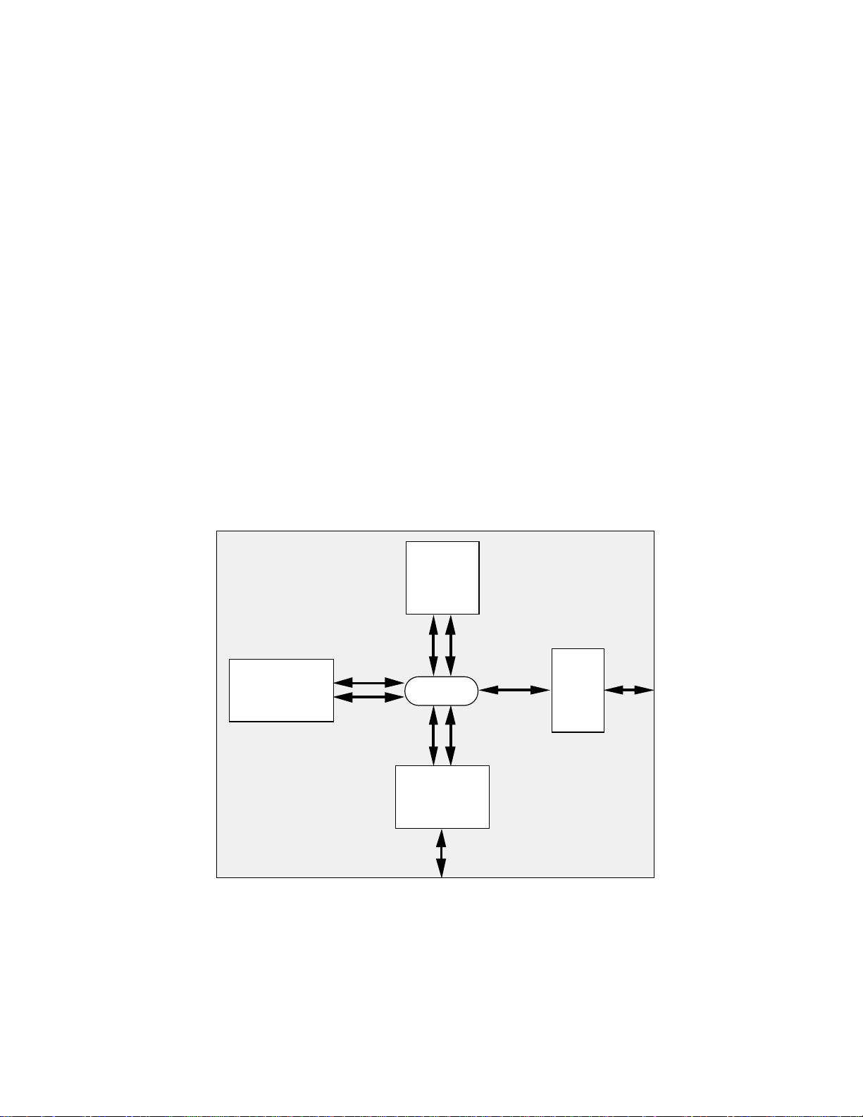
1
Introduction
Figure 1.2 also shows the three on-chip buses of the ADSP-2106x:
the PM bus (program memory), DM bus (data memory), and I/O bus.
The PM bus is used to access either instructions or data. During a
single cycle the processor can access two data operands, one over the
PM bus and one over the DM bus, an instruction (from the cache), and
perform a DMA transfer.
The ADSP-2106x’s external port provides the processor’s interface to
external memory, memory-mapped I/O, a host processor, and
additional multiprocessing ADSP-2106xs. The external port performs
internal and external bus arbitration as well as supplying control
signals to shared, global memory and I/O devices.
Figure 1.3 illustrates a typical single-processor system. A
multiprocessor system is shown in Chapter 7, Multiprocessing.
Dual-Ported,
Multi-Access
Memory
1 – 2
Numeric Processor
Figure 1.1 Super Harvard Architecture
Crossbar Bus
Interconnect
I/O Processor
&
DMA Controller
Parallel
System
Bus
Port
Page 27
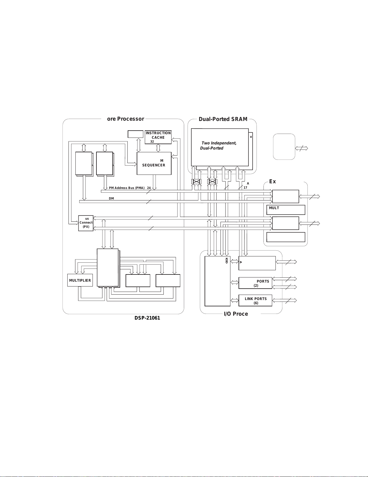
1Introduction
A
A
A
A
DAG1
8 x 4 x 32
Bus
Connect
(PX)
MULTIPLIER
Core Processor
DAG2
8 x 4 x 24
PM Address Bus (PMA) 24
DM Address Bus (DMA) 32
PM Data Bus (PMD)
DM Data Bus (DMD)
DATA
REGISTER
FILE
16 x 40-Bit
TIMER
BARREL
SHIFTER
INSTRUCTION
CACHE
32 x 48-Bit
PROGRAM
SEQUENCER
48
32/40
ALU
Dual-Ported SRAM
Two Independent,
Dual-Ported Blocks
PROCESSOR PORT I/O PORT
ADDR
DATA
DATA
IOD
48
PMD
DMD
EPD
IOD
AA
IOP
AA
REGISTERS
Control,
AA
Status, &
Data Buffers
AA
BLOCK 0
BLOCK 1
ADDR
IOA
17
EPA
IOA
CONTROLLER
SERIAL PORTS
(2)
LINK PORTS
*
(6)
Emulation
External Port
PMA
EPA
DMA
MULTIPROCESSOR
INTERFACE
PMD
EPD
DMD
HOST INTERFACE
DMA
JTAG
Test &
Addr
Bus
Mux
Data
Bus
Mux
7
32
48
4
6
6
36
* not available on the ADSP-21061
I/O Processor
Figure 1.2 ADSP-2106x SHARC Block Diagram
This user’s manual contains architectural information and an
instruction set description required for the design and programming of
ADSP-2106x-based systems. In addition to this manual, hardware
designers should refer to the ADSP-21060/62 Data Sheet and the
ADSP-21061 Data Sheet for timing, electrical, and package
specifications.
1 – 3
Page 28
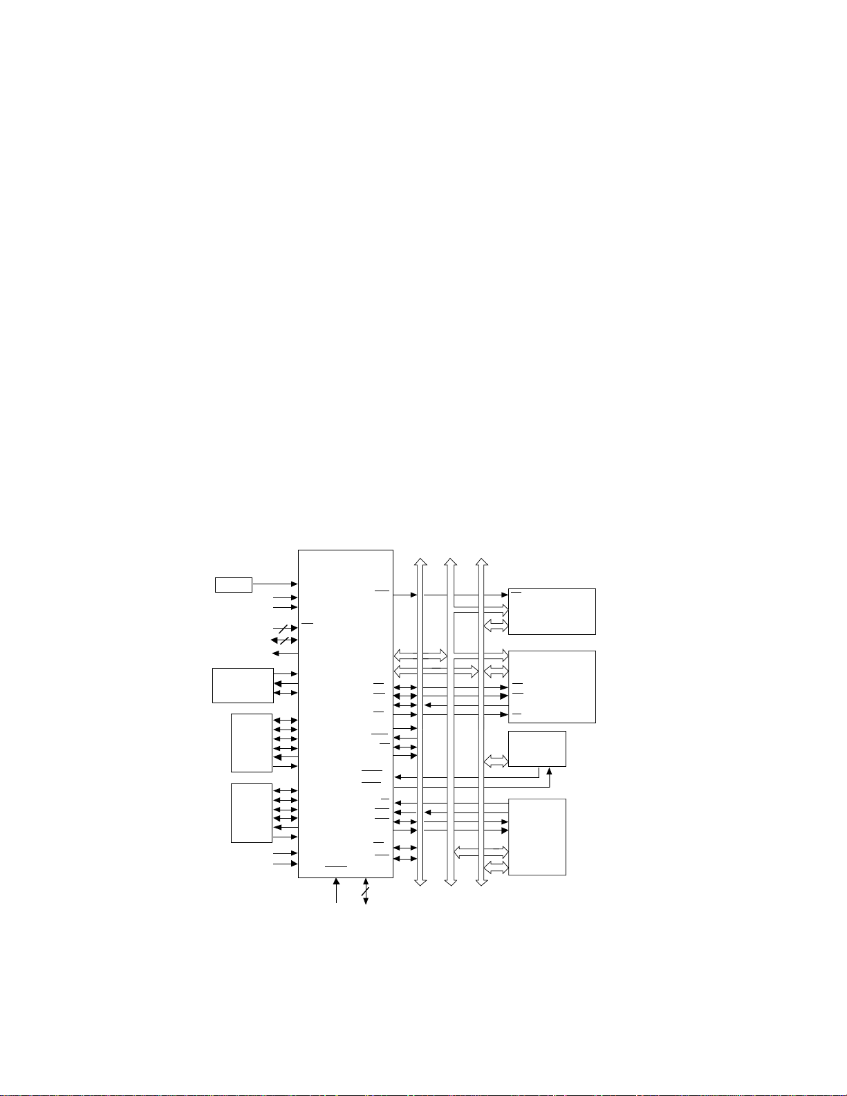
1
Introduction
This manual covers three ADSP-2106x processors: the ADSP-21060,
ADSP-21062, and ADSP-21061. The ADSP-21060 contains 4 megabits of onchip SRAM, the ADSP-21062 contains 2 megabits, and the ADSP-21061
contains 1 megabit. The Memory chapter of this manual describes the
differences in memory architecture and programming considerations of the
three processors. All three processors are code- and function-compatible
with the ADSP-21020 processor. With the exception of memory size, the
ADSP-21060 and ADSP-21062 are identical in all other aspects as well.
Besides memory size, there are four differences between these two
processors and the ADSP-21061:
• No link ports on the ADSP-21061
• 6 DMA channels — 4 for serial port and 2 for external port (instead of 4)
• Additional features and changes in DMA for the serial port
• New idle 16 instruction for a further reduced power mode
These differences are described in detail in the DMA, Serial Port, and
Program Sequencer chapters.
ADSP-2106x
1x CLOCK
LINK DEVICES
(6 Maximum)
(OPTIONAL)
SERIAL
DEVICE
(OPTIONAL)
SERIAL
DEVICE
(OPTIONAL)
CLKIN
EBOOT
LBOOT
3
IRQ
2-0
4
FLAG
3-0
TIMEXP
LxCLK
LxACK
LxDAT
3-0
TCLK0
RCLK0
TFS0
RFS0
DT0
DR0
TCLK1
RCLK1
TFS1
RFS1
DT1
DR1
RPBA
ID
2-0
RESET
ADDR
DATA
RD
WR
ACK
MS
PAGE
SBTS
ADRCLK
DMAR
DMAG
REDY
BR
JTAG
7
BMS
31-0
47-0
SW
1-2
1-2
CS
HBR
HBG
CPA
CS
BOOT
ADDR
EPROM
(OPTIONAL)
DATA
DATA
ADDR
DATA
MEMORY &
PERIPHERALS
OE
(OPTIONAL)
WE
ACK
CS
DMA DEVICE
(OPTIONAL)
DATA
HOST
PROCESSOR
INTERFACE
(OPTIONAL)
ADDR
DATA
ADDRESS
CONTROL
3-0
1-6
1 – 4
Figure 1.3 ADSP-2106x System
Page 29

1.2 ADSP-21000 FAMILY FEATURES & BENEFITS
The ADSP-2106x SHARC processors belong to the ADSP-21000 Family of
floating-point digital signal processors (DSPs). The ADSP-21000
Family architecture further addresses the five central requirements for
DSPs established in the ADSP-2100 Family of 16-bit fixed-point DSPs:
• Fast, flexible arithmetic computation units
• Unconstrained data flow to and from the computation units
• Extended precision and dynamic range in the computation units
• Dual address generators
• Efficient program sequencing
Fast, Flexible Arithmetic. The ADSP-21000 Family processors execute
all instructions in a single cycle. They provide both fast cycle times and
a complete set of arithmetic operations including Seed 1/X, Seed 1/√
Min, Max, Clip, Shift, and Rotate, in addition to the traditional
multiplication, addition, subtraction, and combined multiplication/
addition. The processors are IEEE floating-point compatible and allow
either interrupt on arithmetic exception or latched status exception
handling.
Unconstrained Data Flow. The ADSP-2106x has an enhanced Harvard
architecture combined with a 10-port data register file. In every cycle:
X
,
1Introduction
• Two operands can be read or written to or from the register file,
• Two operands can be supplied to the ALU,
• Two operands can be supplied to the multiplier, and
• Two results can be received from the ALU and multiplier.
The processor’s 48-bit orthogonal instruction word supports fully
parallel data transfer and arithmetic operations in the same instruction.
40-Bit Extended Precision. The ADSP-21000 Family processors handle
32-bit IEEE floating-point format, 32-bit integer and fractional formats
(twos-complement and unsigned), and extended-precision 40-bit IEEE
floating-point format. The processors carry extended precision
throughout their computation units, limiting intermediate data
truncation errors. When working with data on-chip, the
extended-precision 32-bit mantissa can be transferred to and from all
computation units. The 40-bit data bus may be extended off-chip if
desired. The fixed-point formats have an 80-bit accumulator for true
32-bit fixed-point computations.
1 – 5
Page 30

1
Introduction
Dual Address Generators. The ADSP-21000 Family processors have
two data address generators (DAGs) that provide immediate or
indirect (pre- and post-modify) addressing. Modulus and bit-reverse
operations are supported with no constraints on data buffer placement.
Efficient Program Sequencing. In addition to zero-overhead loops, the
ADSP-21000 Family processors support single-cycle setup and exit for
loops. Loops are both nestable (six levels in hardware) and
interruptable. The processors support both delayed and non-delayed
branches.
1.2.1 System-Level Enhancements
The ADSP-21000 Family processors include several enhancements that
simplify system development. The enhancements occur in three key
areas:
• Architectural features supporting high-level languages and operating
systems
• IEEE 1149.1 JTAG serial scan path and on-chip emulation features
• Support of IEEE floating-point formats
High Level Languages. The ADSP-21000 Family architecture has
several features that directly support high-level language compilers
and operating systems:
1 – 6
• General purpose data and address register files
• 32-bit native data types
• Large address space
• Pre- and post-modify addressing
• Unconstrained circular data buffer placement
• On-chip program, loop, and interrupt stacks
Additionally, the ADSP-21000 Family architecture is designed
specifically to support ANSI-standard Numerical C extensions—the
first compiled language to support vector data types and operators for
numeric and signal processing.
Serial Scan and Emulation Features. The ADSP-21000 Family
processors support the IEEE standard P1149.1 Joint Test Action Group
(JTAG) standard for system test. This standard defines a method for
serially scanning the I/O status of each component in a system. The
JTAG serial port is also used by the ADSP-2106x EZ-ICE to gain access
to the processor’s on-chip emulation features.
Page 31

IEEE Formats. The ADSP-21000 Family processors support IEEE
floating-point data formats. This means that algorithms developed on
IEEE-compatible processors and workstations are portable across
processors without concern for possible instability introduced by
biased rounding or inconsistent error handling.
1.2.2 Why Floating-Point DSP?
A digital signal processor’s data format determines its ability to handle
signals of differing precision, dynamic range, and signal-to-noise
ratios. However, ease-of-use and time-to-market considerations are
often equally important.
Precision. The number of bits of precision of A/D converters has
continued to increase, and the trend is for both precision and sampling
rates to increase.
Dynamic Range. Compression and decompression algorithms have
traditionally operated on signals of known bandwidth. These
algorithms were developed to behave regularly, to keep costs down
and implementations easy. Increasingly, however, the trend in
algorithm development is not to constrain the regularity and dynamic
range of intermediate results. Adaptive filtering and imaging are two
applications requiring wide dynamic range.
1Introduction
Signal-to-Noise Ratio. Radar, sonar and even commercial applications
like speech recognition require wide dynamic range in order to discern
selected signals from noisy environments.
Ease-of-Use. In general, 32-bit floating-point DSPs are easier to use
and allow a quicker time-to-market than 16-bit fixed-point processors.
The extent to which this is true depends on the floating-point
processor’s architecture. Consistency with IEEE workstation
simulations and the elimination of scaling are two clear ease-of-use
advantages. High-level language programmability, large address
spaces, and wide dynamic range allow system development time to be
spent on algorithms and signal processing concerns rather than
assembly language coding, code paging, and error handling.
1 – 7
Page 32

1
Introduction
1.3 ADSP-2106X ARCHITECTURE
The following sections summarize the features of the ADSP-2106x
SHARC architecture. These features are described in greater detail in
succeeding chapters.
1.3.1 Core Processor
The core processor of the ADSP-2106x consists of three computation
units, a program sequencer, two data address generators, timer,
instruction cache, and data register file.
1.3.1.1 Computation Units
The ADSP-2106x core processor contains three independent
computation units: an ALU, a multiplier with a fixed-point
accumulator, and a shifter. For meeting a wide variety of processing
needs, the computation units process data in three formats: 32-bit
fixed-point, 32-bit floating-point and 40-bit floating-point. The floatingpoint operations are single-precision IEEE-compatible. The 32-bit
floating-point format is the standard IEEE format, whereas the 40-bit
IEEE extended-precision format has eight additional LSBs of mantissa
for greater accuracy.
The ALU performs a standard set of arithmetic and logic operations in
both fixed-point and floating-point formats. The multiplier performs
floating-point and fixed-point multiplication as well as fixed-point
multiply/add and multiply/subtract operations. The shifter performs
logical and arithmetic shifts, bit manipulation, field deposit and
extraction and exponent derivation operations on 32-bit operands.
1 – 8
The computation units perform single-cycle operations; there is no
computation pipeline. The units are connected in parallel rather than
serially. The output of any unit may be the input of any unit on the
next cycle. In a multifunction computation, the ALU and multiplier
perform independent, simultaneous operations.
1.3.1.2 Data Register File
A general-purpose data register file is used for transferring data
between the computation units and the data buses, and for storing
intermediate results. The register file has two sets (primary and
alternate) of sixteen registers each, for fast context switching. All of the
registers are 40 bits wide. The register file, combined with the core
processor’s Harvard architecture, allows unconstrained data flow
between computation units and internal memory.
Page 33

1.3.1.3 Program Sequencer & Data Address Generators
Two dedicated address generators and a program sequencer supply
addresses for memory accesses. Together the sequencer and data
address generators allow computational operations to execute with
maximum efficiency since the computation units can be devoted
exclusively to processing data. With its instruction cache, the
ADSP-2106x can simultaneously fetch an instruction (from the cache)
and access two data operands (from memory). The data address
generators implement circular data buffers in hardware.
The program sequencer supplies instruction addresses to program
memory. It controls loop iterations and evaluates conditional
instructions. With an internal loop counter and loop stack, the
ADSP-2106x executes looped code with zero overhead. No explicit
jump instructions are required to loop or to decrement and test the
counter.
The ADSP-2106x achieves its fast execution rate by means of pipelined
fetch, decode and execute cycles. If external memories are used, they are
allowed more time to complete an access than if there were no decode
cycle.
1Introduction
The data address generators (DAGs) provide memory addresses when
data is transferred between memory and registers. Dual data address
generators enable the processor to output simultaneous addresses for
two operand reads or writes. DAG1 supplies 32-bit addresses to data
memory. DAG2 supplies 24-bit addresses to program memory for
program memory data accesses.
Each DAG keeps track of up to eight address pointers, eight modifiers
and eight length values. A pointer used for indirect addressing can be
modified by a value in a specified register, either before (pre-modify)
or after (post-modify) the access. A length value may be associated
with each pointer to perform automatic modulo addressing for circular
data buffers; the circular buffers can be located at arbitrary boundaries
in memory. Each DAG register has an alternate register that can be
activated for fast context switching.
Circular buffers allow efficient implementation of delay lines and other
data structures required in digital signal processing, and are
commonly used in digital filters and Fourier transforms. The DAGs
automatically handle address pointer wraparound, reducing overhead,
increasing performance, and simplifying implementation.
1 – 9
Page 34

1
Introduction
1.3.1.4 Instruction Cache
The program sequencer includes a 32-word instruction cache that
enables three-bus operation for fetching an instruction and two data
values. The cache is selective—only instructions whose fetches conflict
with program memory data accesses are cached. This allows full-speed
execution of core, looped operations such as digital filter
multiply-accumulates and FFT butterfly processing.
1.3.1.5 Interrupts
The ADSP-2106x has four external hardware interrupts: three
IRQ
general-purpose interrupts,
The processor also has internally generated interrupts for the timer,
DMA controller operations, circular buffer overflow, stack overflows,
arithmetic exceptions, multiprocessor vector interrupts, and
user-defined software interrupts.
For the general-purpose external interrupts and the internal timer
interrupt, the ADSP-2106x automatically stacks the arithmetic status
and mode (MODE1) registers in parallel with the interrupt servicing,
allowing four nesting levels of very fast service for these interrupts.
, and a special interrupt for reset.
2-0
1.3.1.6 Timer
The programmable interval timer provides periodic interrupt
generation. When enabled, the timer decrements a 32-bit count register
every cycle. When this count register reaches zero, the ADSP-2106x
generates an interrupt and asserts its TIMEXP output. The count
register is automatically reloaded from a 32-bit period register and the
count resumes immediately.
1 – 10
1.3.1.7 Core Processor Buses
The processor core has four buses: Program Memory Address, Data
Memory Address, Program Memory Data, and Data Memory Data.
On the ADSP-2106x processors, data memory stores data operands
while program memory is used to store both instructions and data
(filter coefficients, for example)—this allows dual data fetches, when
the instruction is supplied by the cache.
Page 35

The PM Address bus and DM Address bus are used to transfer the
addresses for instructions and data. The PM Data bus and DM Data
bus are used to transfer the data or instructions stored in each type of
memory. The PM Address bus is 24 bits wide allowing access of up to
16M words of mixed instructions and data. The PM Data bus is 48 bits
wide to accommodate the 48-bit instruction width. Fixed-point and
single-precision floating-point data is aligned to the upper 32 bits of
the PM Data bus.
The DM Address bus is 32 bits wide allowing direct access of up to
4G words of data. The DM Data bus is 40 bits wide. Fixed-point and
single-precision floating-point data is aligned to the upper 32 bits of
the DM Data bus. The DM Data bus provides a path for the contents of
any register in the processor to be transferred to any other register or
to any data memory location in a single cycle. The data memory
address comes from one of two sources: an absolute value specified in
the instruction code (direct addressing) or the output of a data address
generator (indirect addressing).
1.3.1.8 Internal Data Transfers
Nearly every register in the core processor of the ADSP-2106x is
classified as a universal register. Instructions are provided for
transferring data between any two universal registers or between a
universal register and memory. This includes control registers and
status registers, as well as the data registers in the register file.
1Introduction
The PX bus connect registers permit data to be passed between the
48-bit PM Data bus and the 40-bit DM Data bus or between the 40-bit
register file and the PM Data bus. These registers contain hardware to
handle the 8-bit width difference.
1.3.1.9 Context Switching
Many of the processor’s registers have alternate registers that can be
activated during interrupt servicing to facilitate a fast context switch.
The data registers in the register file, the DAG registers, and the
multiplier result register all have alternates. Registers active at reset
are called primary registers, while the others are called alternate (or
secondary) registers. Control bits in a mode control register determine
which set of registers is active at any particular time.
1 – 11
Page 36

1
Introduction
1.3.1.10 Instruction Set
The ADSP-21000 Family instruction set provides a wide variety of
programming capabilities. Multifunction instructions enable
computations in parallel with data transfers, as well as simultaneous
multiplier and ALU operations. The addressing power of the
ADSP-2106x gives you flexibility in moving data both internally and
externally. Every instruction can be executed in a single processor
cycle. The ADSP-21000 Family assembly language uses an algebraic
syntax for ease of coding and readability. A comprehensive set of
development tools supports program development.
1.3.2 Dual-Ported Internal Memory
The ADSP-21060 contains 4 megabits of on-chip SRAM, organized as
two blocks of 2 Mbits each, which can be configured for different
combinations of code and data storage. The ADSP-21062 includes a
2 Mbit SRAM, organized as two 1 Mbit blocks. Each memory block is
dual-ported for single-cycle, independent accesses by the core
processor and I/O processor or DMA controller. The dual-ported
memory and separate on-chip buses allow two data transfers from the
core and one from I/O, all in a single cycle.
All of the memory can be accessed as 16-bit, 32-bit, or 48-bit words.
On the ADSP-21060, the memory can be configured as a maximum of
128K words of 32-bit data, 256K words of 16-bit data, 80K words of
48-bit instructions (and 40-bit data), or combinations of different word
sizes up to 4 megabits. On the ADSP-21062, the memory can be
configured as a maximum of 64K words of 32-bit data, 128K words of
16-bit data, 40K words of 48-bit instructions (and 40-bit data), or
combinations of different word sizes up to 2 megabits. On the ADSP21061, the memory can be configured as a maximum of 32K words of
32-bit data, 64K words of 16-bit data, 16K words of 48-bit instructions
(and 40-bit data), or combinations of different word sizes up to 1
megabit.
1 – 12
A 16-bit floating-point storage format is supported which effectively
doubles the amount of data that may be stored on chip. Conversion
between the 32-bit floating-point and 16-bit floating-point formats is
done in a single instruction.
Page 37

While each memory block can store combinations of code and data,
accesses are most efficient when one block stores data, using the
DM bus for transfers, and the other block stores instructions and data,
using the PM bus for transfers. Using the DM bus and PM bus in this
way, with one dedicated to each memory block, assures single-cycle
execution with two data transfers. In this case, the instruction must be
available in the cache. Single-cycle execution is also maintained when
one of the data operands is transferred to or from off-chip, via the
ADSP-2106x’s external port.
1.3.3 External Memory & Peripherals Interface
The ADSP-2106x’s external port provides the processor’s interface to
off-chip memory and peripherals. The 4-gigaword off-chip address
space is included in the ADSP-2106x’s unified address space. The
separate on-chip buses—for PM addresses, PM data, DM addresses,
DM data, I/O addresses, and I/O data—are multiplexed at the
external port to create an external system bus with a single 32-bit
address bus and a single 48-bit data bus. External SRAM can be either
16, 32, or 48 bits wide; the ADSP-2106x’s on-chip DMA controller
automatically packs external data into the appropriate word width,
either 48-bit instructions or 32-bit data.
1Introduction
Addressing of external memory devices is facilitated by on-chip
decoding of high-order address lines to generate memory bank select
signals. Separate control lines are also generated for simplified
addressing of page-mode DRAM. The ADSP-2106x provides
programmable memory wait states and external memory acknowledge
controls to allow interfacing to DRAM and peripherals with variable
access, hold, and disable time requirements.
1.3.4 Host Processor Interface
The ADSP-2106x’s host interface allows easy connection to standard
microprocessor buses, both 16-bit and 32-bit, with little additional
hardware required. Asynchronous transfers at speeds up to the full
clock rate of the ADSP-2106x are supported. The host interface is
accessed through the ADSP-2106x’s external port and is memorymapped into the unified address space. Four channels of DMA are
available for the host interface; code and data transfers are
accomplished with low software overhead. The host can directly read
and write the internal memory of the ADSP-2106x, and can access the
DMA channel setup and mailbox registers. Vector interrupt support is
provided for efficient execution of host commands.
1 – 13
Page 38

1
Introduction
1.3.5 Multiprocessing
The ADSP-2106x offers powerful features tailored to multiprocessing
DSP systems. The unified address space allows direct interprocessor
accesses of each ADSP-2106x’s internal memory. Distributed bus
arbitration logic is included on-chip for simple, glueless connection of
systems containing up to six ADSP-2106xs and a host processor.
Master processor changeover incurs only one cycle of overhead. Bus
arbitration is selectable as either fixed or rotating priority. Processor
bus lock allows indivisible read-modify-write sequences for semaphores.
A vector interrupt capability is provided for interprocessor commands.
Maximum throughput for interprocessor data transfer is
240 Mbytes/sec over the link ports or external port. Broadcast writes
allow simultaneous transmission of data to all ADSP-2106xs and can
be used to implement reflective semaphores.
1.3.6 I/O Processor
The ADSP-2106x’s I/O Processor (IOP) includes two serial ports, six
4-bit link ports, and a DMA controller.
1.3.6.1 Serial Ports
The ADSP-2106x features two synchronous serial ports that provide an
inexpensive interface to a wide variety of digital and mixed-signal
peripheral devices. The serial ports can operate at the full clock rate of
the processor, providing each with a maximum data rate of 40 Mbit/s.
Independent transmit and receive functions provide greater flexibility
for serial communications. Serial port data can be automatically
transferred to and from on-chip memory via DMA. Each of the serial
ports offers a TDM multichannel mode.
1 – 14
The serial ports can operate with little-endian or big-endian
transmission formats, with word lengths selectable from 3 to 32 bits.
They offer selectable synchronization and transmit modes as well as
optional µ-law or A-law companding. Serial port clocks and frame
syncs can be internally or externally generated.
Page 39

1.3.6.2 Link Ports
The ADSP-21062 and ADSP-21060 feature six 4-bit link ports that
provide additional I/O capabilities. The link ports can be clocked twice
per cycle, allowing each to transfer 8 bits per cycle. Link port I/O is
especially useful for point-to-point interprocessor communication in
multiprocessing systems.
The link ports can operate independently and simultaneously, with a
maximum data throughput of 240 Mbytes/s. Link port data is packed
into 32-bit or 48-bit words, and can be directly read by the core
processor or DMA-transferred to on-chip memory. Each link port has
its own double-buffered input and output registers.
Clock/acknowledge handshaking controls link port transfers.
Transfers are programmable as either transmit or receive.
There are no link ports on the ADSP-21061.
1.3.6.3 DMA Controller
The ADSP-2106x’s on-chip DMA controller allows zero-overhead data
transfers without processor intervention. The DMA controller operates
independently and invisibly to the processor core, allowing DMA
operations to occur while the core is simultaneously executing its
program. Both code and data can be downloaded to the ADSP-2106x
using DMA transfers.
1Introduction
DMA transfers can occur between the ADSP-2106x’s internal memory
and external memory, external peripherals, or a host processor. DMA
transfers can also occur between the ADSP-2106x’s internal memory
and its serial ports or link ports. DMA transfers between external
memory and external peripheral devices are another option. External
bus packing to 16, 32, or 48-bit words is automatically performed
during DMA transfers.
Ten channels of DMA are available on the ADSP-21060 and
ADSP-21062—two via the link ports, four via the serial ports, and four
via the processor’s external port (for either host processor, other
ADSP-2106xs, memory or I/O transfers). Four additional link port
DMA channels are shared with serial port 1 and the external port.
There are six channels of DMA available on the ADSP-21061—four via
the serial ports and two via the external port. Asynchronous off-chip
peripherals can control two DMA channels using DMA Request/Grant
DMAR
lines (
generation upon completion of DMA transfers and DMA chaining for
automatic linked DMA transfers.
1-2
,
DMAG
). Other DMA features include interrupt
1-2
1 – 15
Page 40

1
Introduction
The ten DMA channels of the ADSP-21060 and ADSP-21062 are
numbered as shown below:
DMA Data
Channel# Buffer Description
DMA Channel 0 RX0 Serial Port 0 Receive
DMA Channel 1 RX1 (or LBUF0) Serial Port 1 Receive (or Link Buffer 0)
DMA Channel 2 TX0 Serial Port 0 Transmit
DMA Channel 3 TX1 (or LBUF1) Serial Port 1 Transmit (or Link Buffer 1)
DMA Channel 4 LBUF2 Link Buffer 2
DMA Channel 5 LBUF3 Link Buffer 3
DMA Channel 6 EPB0 (or LBUF4) Ext. Port FIFO Buffer 0 (or Link Buffer 4)
DMA Channel 7 * EPB1 (or LBUF5) Ext. Port FIFO Buffer 1 (or Link Buffer 5)
DMA Channel 8 * EPB2 Ext. Port FIFO Buffer 2
DMA Channel 9 EPB3 Ext. Port FIFO Buffer 3
*
DMAR1
DMAR2
and
and
DMAG1
DMAG2
are handshake controls for DMA Channel 7.
are handshake controls for DMA Channel 8.
1.3.6.4 Booting
The internal memory of the ADSP-2106x can be booted at system
powerup from an 8-bit EPROM or a host processor. Additionally, the
ADSP-21060 and the ADSP-21062 can also be booted through one of
the link ports. Selection of the boot source is controlled by the
EBOOT, and LBOOT pins. Both 32-bit and 16-bit host processors can
be used for booting.
BMS
,
1 – 16
1.4 DEVELOPMENT TOOLS
The ADSP-2106x is supported with a complete set of software and
hardware development tools, including an EZ-LAB
Board, EZ-ICE
development software provides tools for programming and debugging
applications in both assembly language and C. The EZ-ICE emulator
allows system integration and hardware/software debugging. Figure
1.4 shows the process of developing an application using the
development tools.
The development software includes an ANSI C Compiler. The
compiler includes Numerical C extensions based on the work of the
ANSI NCEG committee (Numerical C Extensions Group).
In-Circuit Emulator, and development software. The
Evaluation
Page 41

Numerical C provides extensions to the C language for array selection,
vector math operations, complex data types, circular pointers, and
variably-dimensioned arrays. Other components of the development
software include a C Runtime Library with custom DSP functions, C
and assembly language Debugger, Assembler, Assembly Library/
Librarian, Linker, and Simulator.
1Introduction
Step 1:
DESCRIBE ARCHITECTURE
Step 2:
GENERATE CODE
Step 3:
DEBUG SOFTWARE
Step 4:
DEBUG IN TARGET SYSTEM
Step 5:
MANUFACTURE FINAL SYSTEM
= User File or Hardware
C Source
File
ANSI
C COMPILER
EZ-LAB EVALUATION BOARD
3RD-PARTY PC PLUG-IN CARD
Tested &
Debugged
DSP System
Assembler
Source File
or
EZ-ICE EMULATOR
EPROM/Host/
Link Boot File
= Software Development Tools
Figure 1.4 System Design and Development Process
ASSEMBLER
SOFTWARE
SIMULATOR
BOOT LOADER
System
Architecture
LINKER
Target
Board
File
Executable
File
= Hardware Development Tools
1 – 17
Page 42

1
Introduction
The ADSP-2106x EZ-ICE Emulator uses the IEEE 1149.1 JTAG test
access port of the ADSP-2106x processor to monitor and control the
target board processor during emulation. The EZ-ICE provides fullspeed emulation, allowing inspection and modification of memory,
registers, and processor stacks. Non-intrusive in-circuit emulation is
assured by the use of the processor’s JTAG interface—the emulator
does not affect target system loading or timing.
Further details and ordering information are available in the
ADSP-21000 Family Hardware & Software Development Tools data sheet.
This data sheet can be requested from any Analog Devices sales office
or distributor.
1.5 MESH MULTIPROCESSING
Mesh multiprocessing is a parallel processing system architecture that
offers high throughput, system flexibility, and software simplicity. The
ADSP-21060 and ADSP-21062 SHARC processors include features
which specifically support this system architecture. Mesh
multiprocessing systems are suited to a wide variety of applications
including wide-area airborne radar systems, interactive medical
imaging, virtual reality, high-speed engineering simulations, neural
networks, and solutions of large systems of linear equations.
1 – 18
1.6 ADDITIONAL LITERATURE
The following publications can be ordered from any Analog Devices
sales office.
ADSP-21060/62 SHARC Data Sheet
ADSP-21061 SHARC Data Sheet
ADSP-21000 Family Hardware & Software Development Tools Data Sheet
ADSP-21000 Family Assembler Tools & Simulator Manual
ADSP-21000 Family C Tools Manual
ADSP-21000 Family C Runtime Library Manual
ADSP-21000 Family Applications Handbook, Vol. 1
Page 43

2.1 OVERVIEW
The computation units of the ADSP-2106x provide the numeric processing
power for performing DSP algorithms. The ADSP-2106x contains three
computation units: an arithmetic/logic unit (ALU), a multiplier and a
shifter. Both fixed-point and floating-point operations are supported by
the processor. Each computation unit executes instructions in a single
cycle.
The ALU performs a standard set of arithmetic and logic operations in
both fixed-point and floating-point formats. The multiplier performs
floating-point and fixed-point multiplication as well as fixed-point
multiply/add and multiply/subtract operations. The shifter performs
logical and arithmetic shifts, bit manipulation, field deposit and extraction
operations on 32-bit operands and can derive exponents as well.
2Computation Units
The computation units are architecturally arranged in parallel, as shown
in Figure 2.1 on the next page. The output of any computation unit may be
the input of any computation unit on the next cycle. The computation
units input data from and output data to a 10-port register file that
consists of sixteen primary registers and sixteen alternate registers. The
register file is accessible to the ADSP-2106x program and data memory
data buses for transferring data between the computation units and
external memory or other parts of the processor.
The individual registers of the register file are prefixed with an “F” when
used in floating-point computations (in assembly language source code).
The registers are prefixed with an “R” when used in fixed-point
computations. The following instructions, for example, use the same
registers:
F0=F1 * F2; floating-point multiply
R0=R1 * R2; fixed-point multiply
The F and R prefixes do not affect the 32-bit (or 40-bit) data transfer; they
only determine how the ALU, multiplier, or shifter treat the data. The F or
R may be either uppercase or lowercase; the assembler is case-insensitive.
2 – 1
Page 44

Computation Units
2
PM Data Bus
DM Data Bus
REGISTER
FILE
MULTIPLIER ALUSHIFTER
16 x 40-bit
MR0MR1MR2
Figure 2.1 Computation Units
2 – 2
This chapter covers the following topics:
• Data Formats and Rounding
• ALU Architecture and Functions
• Multiplier Architecture and Functions
• Shifter Architecture and Functions
• Multifunction Computations
• Register File and Data Transfers
2.2 IEEE FLOATING-POINT OPERATIONS
The ADSP-2106x multiplier and ALU support the single-precision
floating-point format specified in the IEEE 754/854 standard. This
standard is described in Appendix C, Numeric Formats. The ADSP-2106x is
IEEE 754/854 compatible for single-precision floating-point operations in
all respects except that:
• The ADSP-2106x does not provide inexact flags.
• NAN (“Not-A-Number”) inputs generate an invalid exception and
return a quiet NAN (all 1s).
Page 45

• Denormal operands are flushed to zero when input to a computation unit
and do not generate an underflow exception. Any denormal or
underflow result from an arithmetic operation is flushed to zero and an
underflow exception is generated.
• Round-to-nearest and round-toward-zero modes are supported.
Rounding to +Infinity and rounding to –Infinity are not supported.
In addition, the ADSP-2106x supports a 40-bit extended precision floatingpoint mode, which has eight additional LSBs of the mantissa and is
compliant with the 754/854 standards; however, results in this format are
more precise than the IEEE single-precision standard specifies.
2.2.1 Extended Floating-Point Precision
Floating-point data can be either 32 or 40 bits wide on the ADSP-2106x.
Extended precision floating-point format (8 bits of exponent and 32 bits of
mantissa) is selected if the RND32 bit in the MODE1 register is cleared (0).
If this bit is set (1), then normal IEEE precision is used (8 bits exponent and
24 bits of mantissa). In this case, the computation unit sets the eight LSBs of
floating-point inputs to zeros before performing the operation. The
mantissa of a result is rounded to 23 bits (not including the hidden bit) and
the 8 LSBs of the 40-bit result are set to zeros to form a 32-bit number that is
equivalent to the IEEE standard result.
2Computation Units
2.2.2 Short Word Floating-Point Format
The ADSP-2106x supports a 16-bit floating-point data type and provides
conversion instructions for it. The short float data format has an 11-bit
mantissa with a four-bit exponent plus sign bit. The 16-bit floating-point
numbers reside in the lower 16 bits of the 32-bit floating-point field.
Two shifter instructions, FPACK and FUNPACK, perform the packing
and unpacking conversions between 32-bit floating-point words and 16-bit
floating-point words. The FPACK instruction converts a 32-bit IEEE
floating-point number to a 16-bit floating-point number. FUNPACK
converts the 16-bit floating-point numbers back to 32-bit IEEE floatingpoint. Each instruction executes in a single cycle.
The short float type supports gradual underflow. This method sacrifices
precision for dynamic range. When packing a number which would have
underflowed, the exponent is set to zero and the mantissa (including
“hidden” 1) is right-shifted the appropriate amount. The packed result is a
denormal which can be unpacked into a normal IEEE floating-point
number.
2 – 3
Page 46

Computation Units
2
2.2.3 Floating-Point Exceptions
The multiplier and ALU each provide exception information when
executing floating-point operations. Each unit updates overflow,
underflow and invalid operation flags in the arithmetic status (ASTAT)
register and in the sticky status (STKY) register. An underflow, overflow
or invalid operation from any unit also generates a maskable interrupt.
Thus, there are three ways to handle floating-point exceptions:
• Interrupts. The exception condition is handled immediately in an
interrupt service routine. You would use this method if it was important
to correct all exceptions as they happen.
• ASTAT register. The exception flags in the ASTAT register pertaining
to a particular arithmetic operation are tested after the operation is
performed. You would use this method to monitor a particular floatingpoint operation.
• STKY register. Exception flags in the STKY register are examined at the
end of a series of operations. If any flags are set, some of the results are
incorrect. You would use this method if exception handling was not
critical.
2 – 4
2.3 FIXED-POINT OPERATIONS
Fixed-point numbers are always represented in 32 bits and are leftjustified (occupy the 32 MSBs) in the 40-bit data fields of the ADSP-2106x.
They may be treated as fractional or integer numbers and as unsigned or
twos-complement. Each computation unit has its own limitations on how
these formats may be mixed for a given operation. The computation units
read 32-bit operands from 40-bit registers, ignoring the 8 LSBs, and write
32-bit results, zeroing the 8 LSBs.
2.4 ROUNDING
Two modes of rounding are supported in the ADSP-2106x: round-towardzero and round-toward-nearest. The rounding modes follow the IEEE 754
standard definitions, which are briefly stated as follows:
Round-Toward-Zero. If the result before rounding is not exactly
representable in the destination format, the rounded result is that number
which is nearer to zero. This is equivalent to truncation.
Page 47

Round-Toward-Nearest. If the result before rounding is not exactly
representable in the destination format, the rounded result is that number
which is nearer to the result before rounding. If the result before rounding is
exactly halfway between two numbers in the destination format (differing by
an LSB), the rounded result is that number which has an LSB equal to zero.
Statistically, rounding up occurs as often as rounding down, so there is no
large sample bias. Because the maximum floating-point value is one LSB less
than the value that represents Infinity, a result that is halfway between the
maximum floating-point value and Infinity rounds to Infinity in this mode.
The rounding mode for all ALU operations and for floating-point multiplier
operations is determined by the TRUNC bit in the MODE1 register. If the
TRUNC bit is set, the round-to-zero mode is selected; otherwise, the roundto-nearest mode is used.
For fixed-point multiplier operations on fractional data, the same two
rounding modes are supported, but only the round-to-nearest operation is
actually performed by the multiplier. Because the multiplier has a local result
register for fixed-point operations, rounding-to-zero is accomplished
implicitly by reading only the upper bits of the result and discarding the
lower bits.
2Computation Units
2.5 ALU
The ALU performs arithmetic operations on fixed-point or floating-point data
and logical operations on fixed-point data. ALU fixed-point instructions
operate on 32-bit fixed-point operands and output 32-bit fixed-point results.
ALU floating-point instructions operate on 32-bit or 40-bit floating-point
operands and output 32-bit or 40-bit floating-point results.
ALU instructions include:
• Floating-point addition, subtraction, add/subtract, average
• Fixed-point addition, subtraction, add/subtract, average
• Floating-point manipulation: binary log, scale, mantissa
• Fixed-point add with carry, subtract with borrow, increment, decrement
• Logical AND, OR, XOR, NOT
• Functions: Absolute value, pass, min, max, clip, compare
• Format conversion
• Reciprocal and reciprocal square root primitives
Dual add/subtract and parallel ALU and multiplier operations are described
under “Multifunction Computations,” later in this chapter.
2 – 5
Page 48

Computation Units
2
2.5.1 ALU Operation
The ALU takes one or two input operands, called the X input and the Y
input, which can be any data registers in the register file. It usually returns
one result; in add/subtract operations it returns two results, and in
compare operations it returns no result (only flags are updated). ALU
results can be returned to any location in the register file.
Input operands are transferred from the register file during the first half of
the cycle. Results are transferred to the register file during the second half
of the cycle. Thus the ALU can read and write the same register file
location in a single cycle.
If the ALU operation is fixed-point, the X input and Y input are each
treated as a 32-bit fixed-point operand. The upper 32 bits from the source
location in the register file are transferred. For fixed-point operations, the
result(s) are always 32-bit fixed-point values. Some floating-point
operations (LOGB, MANT and FIX) can also yield fixed-point results.
Fixed-point results are transferred to the upper 32 bits of register file. The
lower eight bits of the register file destination are cleared.
The format of fixed-point operands and results depends on the operation.
In most arithmetic operations, there is no need to distinguish between
integer and fractional formats. Fixed-point inputs to operations such as
scaling a floating-point value are treated as integers. For purposes of
determining status such as overflow, fixed-point arithmetic operands and
results are treated as twos-complement numbers.
2 – 6
2.5.2 ALU Operating Modes
The ALU is affected by three bits in the MODE1 register; the ALU
saturation bit affects ALU operations that yield fixed-point results, and the
rounding mode and rounding boundary bits affect floating-point
operations in both the ALU and multiplier.
MODE1
Bit Name Function
13 ALUSAT 1=Enable ALU saturation (full scale in fixed-point)
0=Disable ALU saturation
15 TRUNC 1=Truncation; 0=Round to nearest
16 RND32 1=Round to 32 bits; 0=Round to 40 bits
Page 49

2.5.2.1 Saturation Mode
In saturation mode, all positive fixed-point overflows cause the maximum
positive fixed-point number (0x7FFF FFFF) to be returned, and all
negative overflows cause the maximum negative number (0x8000 0000) to
be returned. If the ALUSAT bit is set, fixed-point results that overflow are
saturated. If the ALUSAT bit is cleared, fixed-point results that overflow
are not saturated; the upper 32 bits of the result are returned unaltered.
The ALU overflow flag reflects the ALU result before saturation.
2.5.2.2 Floating-Point Rounding Modes
The ALU supports two IEEE rounding modes. If the TRUNC bit is set, the
ALU rounds a result to zero (truncation). If the TRUNC bit is cleared, the
ALU rounds to nearest.
2.5.2.3 Floating-Point Rounding Boundary
The results of floating-point ALU operations can be either 32-bit or 40-bit
floating-point data on the ADSP-2106x. If the RND32 bit is set, the eight
LSBs of each input operand are flushed to zeros before the ALU operation
is performed (except for the RND operation), and ALU floating-point
results are output in the 32-bit IEEE format. The lower eight bits of the
result are cleared. If the RND32 bit is cleared, the ALU inputs 40-bit
operands unchanged and outputs 40-bit results from floating-point
operations, and all 40 bits are written to the specified register file location.
2Computation Units
In fixed-point to floating-point conversion, the rounding boundary is
always 40 bits even if the RND32 bit is set.
2.5.3 ALU Status Flags
The ALU updates seven status flags in the ASTAT register, shown below,
at the end of each operation. The states of these flags reflect the result of
the most recent ALU operation. The ALU updates the Compare
Accumulation bits in ASTAT at the end of every Compare operation. The
ALU also updates four “sticky” status flags in the STKY register. Once set,
a sticky flag remains high until explicitly cleared.
ASTAT
Bit Name Definition
0 AZ ALU result zero or floating-point underflow
1 AV ALU overflow
2 AN ALU result negative
3 AC ALU fixed-point carry
4 AS ALU X input sign (ABS, MANT operations)
5 AI ALU floating-point invalid operation
10 AF Last ALU operation was a floating-point operation
31-24 CACC Compare Accumulation register (results of last 8 compare
operations)
2 – 7
Page 50

Computation Units
2
STKY
Bit Name Definition
0 AUS ALU floating-point underflow
1 AVS ALU floating-point overflow
2 AOS ALU fixed-point overflow
5 AIS ALU floating-point invalid operation
Flag update occurs at the end of the cycle in which the status is generated
and is available on the next cycle. If a program writes the ASTAT register
or STKY register explicitly in the same cycle that the ALU is performing
an operation, the explicit write to ASTAT or STKY supersedes any flag
update from the ALU operation.
2.5.3.1 ALU Zero Flag (AZ)
The zero flag is determined for all fixed-point and floating-point ALU
operations. AZ is set whenever the result of an ALU operation is zero.
AZ also signifies floating-point underflow; see the next section. It is
otherwise cleared.
2.5.3.2 ALU Underflow Flag (AZ, AUS)
Underflow is determined for all ALU operations that return a floatingpoint result and for floating-point to fixed-point conversion. AUS is set
whenever the result of an ALU operation is smaller than the smallest
number representable in the output format. AZ is set whenever a
floating-point result is smaller than the smallest number representable in
the output format.
2 – 8
2.5.3.3 ALU Negative Flag (AN)
The negative flag is determined for all ALU operations. It is set whenever
the result of an ALU operation is negative. It is otherwise cleared.
2.5.3.4 ALU Overflow Flag (AV, AOS, AVS)
Overflow is determined for all fixed-point and floating-point ALU
operations. For fixed-point results, AV and AOS are set whenever the
XOR of the two most significant bits is a 1; otherwise AV is cleared. For
floating-point results AV and AVS are set whenever the post-rounded
result overflows (unbiased exponent > 127); otherwise AV is cleared.
Page 51

2.5.3.5 ALU Fixed-Point Carry Flag (AC)
The carry flag is determined for all fixed-point ALU operations. For
fixed-point arithmetic operations, AC is set if there is a carry out of most
significant bit of the result, and is otherwise cleared. AC is cleared for
fixed-point logic, PASS, MIN, MAX, COMP, ABS, and CLIP operations.
The ALU reads the AC flag in fixed-point addition with carry and
fixed-point subtraction with carry operations.
2.5.3.6 ALU Sign Flag (AS)
The sign flag is determined for only the fixed-point and floating-point
ABS operations and the MANT operation. AS is set if the input operand is
negative. It is otherwise cleared. The ALU clears AS for all operations
other than ABS and MANT operations; this is different from the operation
of ADSP-2100 family processors, which do not update the AS flag on
operations other than ABS.
2.5.3.7 ALU Invalid Flag (AI)
The invalid flag is determined for all floating-point ALU operations.
AI and AIS are set whenever
• an input operand is a NAN
• an addition of opposite-signed Infinities is attempted
• a subtraction of like-signed Infinities is attempted
• when saturation mode is not set, a floating-point to fixed-point
conversion results in an overflow or operates on an Infinity.
2Computation Units
AI is otherwise cleared.
2.5.3.8 ALU Floating-Point Flag (AF)
AF is determined for all fixed-point and floating-point ALU operations. It
is set if the last operation was a floating-point operation; it is otherwise
cleared.
2.5.3.9 Compare Accumulation
Bits 31-24 in the ASTAT register store the flag results of up to eight ALU
compare operations. These bits form a right-shift register. When an ALU
compare operation is executed, the eight bits are shifted toward the LSB
(bit 24 is lost). The MSB, bit 31, is then written with the result of the
compare operation. If the X operand is greater than the Y operand in the
compare instruction, bit 31 is set; it is cleared otherwise. The accumulated
compare flags can be used to implement 2- and 3-dimensional clipping
operations for graphics applications.
2 – 9
Page 52

Computation Units
2
2.5.4 ALU Instruction Summary
Instruction ASTAT Status Flags STKY Status Flags
Fixed-point: AZ AV AN AC AS AI AF CACC AUS AVS AOS AIS
c Rn = Rx + Ry * * * * 0 0 0 – – – ** –
c Rn = Rx – Ry * * * * 0 0 0 – – – ** –
c Rn = Rx + Ry + CI * * * * 0 0 0 – – – ** –
c Rn = Rx – Ry + CI – 1 * * * * 0 0 0 – – – ** –
Rn = (Rx + Ry)/2 * 0 * * 0 0 0 – – – – –
COMP(Rx, Ry) * 0 * 0 0 0 0 * – – – –
Rn = Rx + CI * * * * 0 0 0 – – – ** –
Rn = Rx + CI – 1 * * * * 0 0 0 – – – ** –
Rn = Rx + 1 * * * * 0 0 0 – – – ** –
Rn = Rx – 1 * * * * 0 0 0 – – – ** –
c Rn = –Rx * * * * 0 0 0 – – – ** –
c Rn = ABS Rx * * 0 0 * 0 0 – – – ** –
Rn = PASS Rx * 0 * 0 0 0 0 – – – – –
c Rn = Rx AND Ry * 0 * 0 0 0 0 – – – – –
c Rn = Rx OR Ry * 0 * 0 0 0 0 – – – – –
c Rn = Rx XOR Ry * 0 * 0 0 0 0 – – – – –
c Rn = NOT Rx * 0 * 0 0 0 0 – – – – –
Rn = MIN(Rx, Ry) * 0 * 0 0 0 0 – – – – –
Rn = MAX(Rx, Ry) * 0 * 0 0 0 0 – – – – –
Rn = CLIP Rx BY Ry * 0 * 0 0 0 0 – – – – –
Floating–point:
Fn = Fx + Fy * * * 0 0 * 1 – ** ** – **
Fn = Fx – Fy * * * 0 0 * 1 – ** ** – **
Fn = ABS (Fx + Fy) * * 0 0 0 * 1 – ** ** – **
Fn = ABS (Fx – Fy) * * 0 0 0 * 1 – ** ** – **
Fn = (Fx + Fy)/2 * 0 * 0 0 * 1 – ** – – **
COMP(Fx, Fy) * 0 * 0 0 * 1 * – – – **
Fn = –Fx * * * 0 0 * 1 – – ** – **
Fn = ABS Fx * * 0 0 * * 1 – – ** – **
Fn = PASS Fx * 0 * 0 0 * 1 – – – – **
Fn = RND Fx * * * 0 0 * 1 – – ** – **
Fn = SCALB Fx BY Ry * * * 0 0 * 1 – ** ** – **
Rn = MANT Fx * * 0 0 * * 1 – – ** – **
Rn = LOGB Fx * * * 0 0 * 1 – – ** – **
Rn = FIX Fx BY Ry * * * 0 0 * 1 – ** ** – **
Rn = FIX Fx * * * 0 0 * 1 – ** ** – **
Fn = FLOAT Rx BY Ry * * * 0 0 0 1 – ** ** – –
Fn = FLOAT Rx * 0 * 0 0 0 1 – – – – –
Fn = RECIPS Fx * * * 0 0 * 1 – ** ** – **
Fn = RSQRTS Fx * * * 0 0 * 1 – – ** – **
Fn = Fx COPYSIGN Fy * 0 * 0 0 * 1 – – – – **
Fn = MIN(Fx, Fy) * 0 * 0 0 * 1 – – – – **
Fn = MAX(Fx, Fy) * 0 * 0 0 * 1 – – – – **
Fn = CLIP Fx BY Fy * 0 * 0 0 * 1 – – – – **
2 – 10
Rn, Rx, Ry = Any register file location; treated as fixed-point
Fn, Fx, Fy = Any register file location; treated as floating-point
c = ADSP-21xx-compatible instruction
* set or cleared, depending on results of instruction
** may be set (but not cleared), depending on results of instruction
– no effect
Page 53

2Computation Units
2.6 MULTIPLIER
The multiplier performs fixed-point or floating-point multiplication and fixedpoint multiply/accumulate operations. Fixed-point multiply/accumulates may
be performed with either cumulative addition or cumulative subtraction.
Floating-point multiply/accumulates can be accomplished through parallel
operation of the ALU and multiplier, using multifunction instructions. See
“Multifunction Computations” later in this chapter.
Multiplier floating-point instructions operate on 32-bit or 40-bit floating-point
operands and output 32-bit or 40-bit floating-point results. Multiplier fixed-point
instructions operate on 32-bit fixed-point data and produce 80-bit results. Inputs
are treated as fractional or integer, unsigned or twos-complement.
Multiplier instructions include:
• Floating-point multiplication
• Fixed-point multiplication
• Fixed-point multiply/accumulate with addition, rounding optional
• Fixed-point multiply/accumulate with subtraction, rounding optional
• Rounding result register
• Saturating result register
• Clearing result register
2.6.1 Multiplier Operation
The multiplier takes two input operands, called the X input and the Y input,
which can be any data registers in the register file. Fixed-point operations can
accumulate fixed-point results in either of two local multiplier result registers
(MR) or write results back to the register file. Results stored in the MR registers
can also be rounded or saturated in separate operations. Floating-point
operations yield floating-point results, which are always written directly back
to the register file.
Input operands are transferred during the first half of the cycle. Results are
transferred during the second half of the cycle. Thus the multiplier can read
and write the same register file location in a single cycle.
If the multiplier operation is fixed-point, inputs taken from the register file are
read from the upper 32 bits of the source location. Fixed-point operands may be
treated as both in integer format or both in fractional format. The format of the
result is the same as the format of the inputs. Each fixed-point operand may be
treated as either an unsigned or a twos-complement number. If both inputs are
fractional and signed, the multiplier automatically shifts the result left one bit to
remove the redundant sign bit. The input data type is specified within the
multiplier instruction.
2 – 11
Page 54

2
MR Register
Computation Units
2.6.2 Fixed-Point Results
Fixed-point operations yield 80-bit results in the MR register. The location
of a result in the 80-bit field depends on whether the result is in fractional or
integer format, as shown in Figure 2.2. If the result is sent directly to the
register file, the 32 bits that have the same format as the input data are
transferred, i.e. bits 63-32 for a fractional result or bits 31-0 for an integer
result. The eight LSBs of the 40-bit register file location are zero-filled.
Fractional results can be rounded-to-nearest before being sent to the register
file, as explained later in this chapter. If rounding is not specified,
discarding bits 31-0 effectively truncates a fractional result (rounds to zero).
0316379
MR2 MR1 MR0
OVERFLOW UNDERFLOW
OVERFLOW
Figure 2.2 Multiplier Fixed-Point Result Placement
FRACTIONAL RESULT
INTEGER RESULTOVERFLOW
2.6.2.1 MR Registers
The entire result can be sent to one of two dedicated 80-bit result registers
(MR). The MR registers have identical format; each is divided into MR2,
MR1 and MR0 registers that can be individually read from or written to
the register file. When data is read from MR2, it is sign-extended to 32 bits
(see Figure 2.3). The eight LSBs of the 40-bit register file location are zerofilled when data is read from MR2, MR1 or MR0 to the register file. Data is
written into MR2, MR1 or MR0 from the 32 MSBs of a register file location;
the eight LSBs are ignored. Data written to MR1 is sign-extended to MR2,
i.e. the MSB of MR1 is repeated in the 16 bits of MR2. Data written to MR0,
however, is not sign-extended.
The two MR registers are designated MRF (foreground) and MRB
(background); foreground refers to those registers currently activated by
the SRCU bit in the MODE1 register, and background refers to those that
are not. In the case that only one MR register is used at a time, the SRCU
bit activates one or the other to facilitate context switching. However,
unlike other registers for which alternate sets exist, both MR register sets
are accessible at the same time. All (fixed-point) accumulation instructions
2 – 12
Page 55

2Computation Units
16 bits
SIGN EXTEND
16 bits
MR2
8 bits
ZEROS
MR1
8 bits32 bits
ZEROS
MR0
Figure 2.3 MR Transfer Formats
may specify either result register for accumulation, regardless of the state of
the SRCU bit. Thus, instead of using the MR registers as a primary and an
alternate, you can use them as two parallel accumulators. This feature
facilitates complex math.
Transfers between MR registers and the register file are considered
computation unit operations, since they involve the multiplier. Thus,
although the syntax for the transfer is the same as for any other transfer to or
from the register file, an MR transfer is placed in an instruction where a
computation is normally specified. For example, the ADSP-2106x can perform
a multiply/accumulate in parallel with a read of data memory, as in:
MRF=MRF-R5*R0, R6=DM(I1,M2);
or it can perform an MR transfer instead of the computation, as in:
8 bits32 bits
ZEROS
R5=MR1F, R6=DM(I1,M2);
2.6.3 Fixed-Point Operations
In addition to multiplication, fixed-point operations include accumulation,
rounding and saturation of fixed-point data. There are three MR register
operations: Clear, Round and Saturate.
2.6.3.1 Clear MR Register
The clear operation resets the specified MR register to zero. This operation is
performed at the start of a multiply/accumulate operation to remove results
left over from the previous operation.
2 – 13
Page 56

Computation Units
2
2.6.3.2 Round MR Register
Rounding of a fixed-point result occurs either as part of a multiply or
multiply/accumulate operation or as an explicit operation on the MR
register. The rounding operation applies only to fractional results (integer
results are not affected) and rounds the 80-bit MR value to nearest at bit
32, i.e. at the MR1-MR0 boundary. The rounded result in MR1 can be sent
either to the register file or back to the same MR register. To round a
fractional result to zero (truncation) instead of to nearest, you would
simply transfer the unrounded result from MR1, discarding the lower 32
bits in MR0.
2.6.3.3 Saturate MR Register On Overflow
The saturate operation sets MR to a maximum value if the MR value has
overflowed. Overflow occurs when the MR value is greater than the
maximum value for the data format (unsigned or twos-complement and
integer or fractional) that is specified in the saturate instruction. There are
six possible maximum values (shown in hexadecimal):
MR2 MR1 MR0
Maximum twos-complement fractional number
0000 7FFF FFFF FFFF FFFF positive
FFFF 8000 0000 0000 0000 negative
Maximum twos-complement integer number
0000 0000 0000 7FFF FFFF positive
FFFF FFFF FFFF 8000 0000 negative
Maximum unsigned fractional number
0000 FFFF FFFF FFFF FFFF
Maximum unsigned integer number
0000 0000 0000 FFFF FFFF
2 – 14
The result from MR saturation can be sent either to the register file or back
to the same MR register.
Page 57

2.6.4 Floating-Point Operating Modes
The multiplier is affected by two mode status bits in the MODE1 register:
the rounding mode and rounding boundary bits, which affect operations
in both the multiplier and the ALU.
MODE1
Bit Name Function
15 TRUNC 1=Truncation; 0=Round to nearest
16 RND32 1=Round to 32 bits; 0=Round to 40 bits
2.6.4.1 Floating-Point Rounding Modes
The multiplier supports two IEEE rounding modes for floating-point
operations. If the TRUNC bit is set, the multiplier rounds a floating-point
result to zero (truncation). If the TRUNC bit is cleared, the multiplier
rounds to nearest.
2.6.4.2 Floating-Point Rounding Boundary
Floating-point multiplier inputs and results can be either 32-bit or 40-bit
floating-point data on the ADSP-2106x. If the RND32 bit is set, the eight
LSBs of each input operand are flushed to zeros before multiplication, and
floating-point results are output in the 32-bit IEEE format, with the lower
eight bits of the 40-bit register file location cleared. The mantissa of the
result is rounded to 23 bits (not including the hidden bit). If the RND32 bit
is cleared, the multiplier inputs full 40-bit values from the register file and
outputs results in the 40-bit extended IEEE format, with the mantissa
rounded to 31 bits not including the hidden bit.
2Computation Units
2.6.5 Multiplier Status Flags
The multiplier updates four status flags at the end of each operation. All
of these flags appear in the ASTAT register. The states of these flags reflect
the result of the most recent multiplier operation. The multiplier also
updates four “sticky” status flags in the STKY register. Once set, a sticky
flag remains high until explicitly cleared.
ASTAT
Bit Name Definition
6 MN Multiplier result negative
7 MV Multiplier overflow
8 MU Multiplier underflow
9 MI Multiplier floating-point invalid operation
2 – 15
Page 58

Computation Units
2
STKY
Bit Name Definition
6 MOS Multiplier fixed-point overflow
7 MVS Multiplier floating-point overflow
8 MUS Multiplier underflow
9 MIS Multiplier floating-point invalid operation
Flag update occurs at the end of the cycle in which the status is generated
and is available on the next cycle. If a program writes the ASTAT register
or STKY register explicitly in the same cycle that the multiplier is
performing an operation, the explicit write to ASTAT or STKY supersedes
any flag update from the multiplier operation.
2.6.5.1 Multiplier Underflow Flag (MU)
Underflow is determined for all fixed-point and floating-point multiplier
operations. It is set whenever the result of a multiplier operation is smaller
than the smallest number representable in the output format. It is
otherwise cleared.
For floating-point results, MU and MUS are set whenever the postrounded result underflows (unbiased exponent < –126). Denormal
operands are treated as Zeros, therefore they never cause underflows.
2 – 16
For fixed-point results, MU and MUS depend on the data format and are
set under the following conditions:
Twos-complement:
Fractional: upper 48 bits all zeros or all ones, lower 32 bits not all zeros
Integer: not possible
Unsigned:
Fractional: upper 48 bits all zeros, lower 32 bits not all zeros
Integer: not possible
If the fixed-point result is sent to an MR register, the underflowed portion
of the result is available in MR0 (fractional result only).
Page 59

2Computation Units
2.6.5.2 Multiplier Negative Flag (MN)
The negative flag is determined for all multiplier operations. MN is set
whenever the result of a multiplier operation is negative. It is otherwise cleared.
2.6.5.3 Multiplier Overflow Flag (MV)
Overflow is determined for all fixed-point and floating-point multiplier
operations.
For floating-point results, MV and MVS are set whenever the post-rounded
result overflows (unbiased exponent > 127).
For fixed-point results, MV and MOS depend on the data format and are set
under the following conditions:
Twos-complement:
Fractional: upper 17 bits of MR not all zeros or all ones
Integer: upper 49 bits of MR not all zeros or all ones
Unsigned:
Fractional: upper 16 bits of MR not all zeros
Integer: upper 48 bits of MR not all zeros
If the fixed-point result is sent to an MR register, the overflowed portion of
the result is available in MR1 and MR2 (integer result) or MR2 only (fractional
result).
2.6.5.4 Multiplier Invalid Flag (MI)
The invalid flag is determined for floating-point multiplication. MI is set
whenever:
• an input operand is a NAN.
• the inputs are Infinity and Zero (note: denormal inputs are treated as Zeros.)
MI is otherwise cleared.
2 – 17
Page 60

Computation Units
2
2.6.6 Multiplier Instruction Summary
Instruction ASTAT Flags STKY Flags
MU MN MV MI MUS MOS MVS MIS
Fixed-Point:
Rn = Rx * Ry ( SSF)
MRF
MRB FR
Rn = MRF + Rx * Ry ( SSF )
Rn = MRB
MRF = MRF FR
MRB = MRB
Rn = MRF – Rx * Ry (
Rn = MRB
MRF = MRF FR
MRB = MRB
Rn = SAT MRF (SI)
Rn = SAT MRB (UI)
MRF = SAT MRF (SF)
MRB = SAT MRB (UF)
Rn = RND MRF (SF)
Rn = RND MRB (UF)
MRF = RND MRF
MRB = RND MRB
MRF= 0 0000 ––––
MRB
MRxF = Rn 0 0 0 0 ––––
MRxB
Rn = MRxF 0 0 0 0 ––––
MRxB
UU I
UUI
SSF )
UUI
***
***
***
***
***
0–**––
0–**––
0–**––
0–**––
0–**––
2 – 18
Floating-Point:
Fn = Fx * Fy
Note: For floating-point multiply/accumulates, see “Multifunction Computations"
* set or cleared, depending on results of instruction
** may be set (but not cleared), depending on results of instruction
– no effect
Rn, Rx, Ry = R15-R0; register file location, treated as fixed-point
Fn, Fx, Fy = F15-F0; register file location, treated as floating-point
MRxF = MR2F, MR1F, MR0F; multiplier result accumulators, foreground
MRxB = MR2B, MR1B, MR0B; multiplier result accumulators, background
**** **
–
** **
Page 61

Multiplier Instruction Summary, cont.
Optional Modifiers for Fixed-Point:
( ❑❑❑ ) S Signed input
Y-input
X-input
rounding
Data format,
U Unsigned input
I Integer input(s)
F Fractional input(s)
FR Fractional inputs, Rounded output
(SF) Default format for 1-input operations
(SSF) Default format for 2-input operations
2.7 SHIFTER
The shifter operates on 32-bit fixed-point operands. Shifter operations
include:
• shifts and rotates from off-scale left to off-scale right
• bit manipulation operations, including bit set, clear, toggle, and test
• bit field manipulation operations including extract and deposit
• support for ADSP-2100 family compatible fixed-point/floating-point
conversion operations (exponent extract, number of leading 1s or 0s)
2.7.1 Shifter Operation
The shifter takes from one to three input operands: the X-input, which is
operated upon; the Y-input, which specifies shift magnitudes, bit field
lengths or bit positions; and the Z-input, which is operated on and
updated (as in, for example, Rn = Rn OR LSHIFT Rx BY Ry). The shifter
returns one output to the register file.
2Computation Units
Input operands are fetched from the upper 32 bits of a register file location
(bits 39-8, as shown in Figure 2.4 on the following page) or from an
immediate value in the instruction. The operands are transferred during
the first half of the cycle. The result is transferred to the upper 32 bits of a
register (with the eight LSBs zero-filled) during the second half of the
cycle. Thus the shifter can read and write the same register file location in
a single cycle.
2 – 19
Page 62

Computation Units
2
The X-input and Z-input are always 32-bit fixed-point values. The Y-input
is a 32-bit fixed-point value or an 8-bit field (shf8), positioned in the
register file as shown in Figure 2.4 below.
Some shifter operations produce 8-bit or 6-bit results. These results are
placed in either the shf8 field or the bit6 field (see Figure 2.5) and are signextended to 32 bits. Thus the shifter always returns a 32-bit result.
32-Bit Y-Input or Result
shf8
8-Bit Y-Input or Result
Figure 2.4 Register File Fields For Shifter Instructions
2.7.2 Bit Field Deposit & Extract Instructions
The shifter’s bit field deposit and bit field extract instructions allow the
manipulation of groups of bits within a 32-bit fixed-point integer word.
039 7
715 039
2 – 20
The Y-input for these instructions specifies two 6-bit values, bit6 and len6,
positioned in the Ry register as shown in Figure 2.5. Bit6 and len6 are
interpreted as positive integers. Bit6 is the starting bit position for the
deposit or extract. Len6 is the bit field length, which specifies how many
bits are deposited or extracted.
13
len6
12-Bit Y-Input
Figure 2.5 Register File Fields For FDEP, FEXT Instructions
bit6
719
039
Page 63

The FDEP (field deposit) instructions take a group of bits from the input
register Rx (starting at the LSB of the 32-bit integer field) and deposit them
anywhere within the result register Rn. The bit6 value specifies the
starting bit position for the deposit. See Figure 2.6.
The FEXT (field extract) instructions extract a group of bits from anywhere
within the input register Rx and place them in the result register Rn
(aligned with the LSB of the 32-bit integer field). The bit6 value specifies
the starting bit position for the extract.
Rn=FDEP Rx BY Ry
2Computation Units
13
Ry
Ry determines length of bit field to take from Rx and starting bit position for deposit in Rn
Rx
len6 = number of bits to take from Rx, starting from LSB of 32-bit field
Rn
bit6 = starting bit position for deposit, referenced from LSB of 32-bit field
deposit field
len6
bit6 reference point
bit6
719
Figure 2.6 Bit Field Deposit Instruction
039
039 7
039 7
2 – 21
Page 64

Computation Units
2
The following field deposit instruction example is pictured in Figure 2.7:
R0=FDEP R1 BY R2;
R0=FDEP R1 BY R2;
R1=0x000000FF00
R2=0x0000021000
39 08162432
R2
00000000 00000000
39 08162432
R1
00000000 00000000 00000000 11111111 00000000
39 08162432
R0
00000000 11111111 00000000 00000000 00000000
00000010 00
len6
010000
00000000
bit6
081624
0x0000 0210 00
len6 = 8
bit6 = 16
0x0000 00FF 00
0x00FF 0000 00
2 – 22
starting bit
position for
deposit
8 bits are taken from R1 and deposited in R0, starting at bit 16.
("Bit 16" is relative to reference point, the LSB of 32-bit integer field.)
Figure 2.7 Bit Field Deposit Example
reference
point
Page 65

The following field extract instruction example is pictured in Figure 2.8:
R3=FEXT R4 BY R5;
R3=FEXT R4 BY R5;
R4=0x8788000000
R5=0x0000021700
39 08162432
R5
00000000 00000000
39 08162432
R4
10000111 10000000
00000010 00
00000000 00000000 00000000
010111
00000000
bit6len6
0816
0x0000 0217 00
len6 = 8
bit6 = 23
0x8788 0000 00
2Computation Units
starting bit position
for extract
39 08162432
R3
00000000 00000000 00000000
8 bits are extracted from R4 and placed in R3, aligned to the LSB of the 32-bit integer field.
00001111
reference
point
00000000
0x0000 000F 00
Figure 2.8 Bit Field Extract Example
2 – 23
Page 66

Computation Units
2
2.7.3 Shifter Status Flags
The shifter returns three status flags at the end of the operation. All of
these flags appear in the ASTAT register. The SZ flag indicates if the
output is zero, the SV flag indicates an overflow, and the SS flag indicates
the sign bit in exponent extract operations.
ASTAT
Bit Name Definition
11 SV Shifter overflow of bits to left of MSB
12 SZ Shifter result zero
13 SS Shifter input sign (for exponent extract only)
Flag update occurs at the end of the cycle in which the status is generated
and is available on the next cycle. If a program writes the ASTAT register
explicitly in the same cycle that the shifter is performing an operation, the
explicit write to ASTAT supersedes any flag update caused by the shift
operation.
2.7.3.1 Shifter Zero Flag (SZ)
SZ is affected by all shifter operations. It is set whenever:
• the result of a shifter operation is zero, or
• a bit test instruction specifies a bit outside of the 32-bit fixed-point field.
2 – 24
SZ is otherwise cleared.
2.7.3.2 Shifter Overflow Flag (SV)
SV is affected by all shifter operations. It is set whenever:
• significant bits are shifted to the left of the 32-bit fixed-point field,
• a bit outside of the 32-bit fixed-point field is tested, set or cleared,
• a field that is partially or wholly to the left of the 32-bit fixed-point field
is extracted, or
• a LEFTZ or LEFTO operation returns a result of 32.
SV is otherwise cleared.
2.7.3.3 Shifter Sign Flag (SS)
SS is affected by all shifter operations. For the two EXP (exponent
extract) operations, it is set if the fixed-point input operand is negative
and cleared if it is positive. For all other shifter operations, SS is
cleared.
Page 67

2.7.4 Shifter Instruction Summary
2Computation Units
Instruction Flags
c Rn = LSHIFT Rx BY Ry * * 0
c Rn = LSHIFT Rx BY <data8> * * 0
c Rn = Rn OR LSHIFT Rx BY Ry * * 0
c Rn = Rn OR LSHIFT Rx BY <data8> * * 0
c Rn = ASHIFT Rx BY Ry * * 0
c Rn = ASHIFT Rx BY<data8> * * 0
c Rn = Rn OR ASHIFT Rx BY Ry * * 0
c Rn = Rn OR ASHIFT Rx BY <data8> * * 0
Rn = ROT Rx BY RY * 0 0
Rn = ROT Rx BY <data8> * 0 0
Rn = BCLR Rx BY Ry * * 0
Rn = BCLR Rx BY <data8> * * 0
Rn = BSET Rx BY Ry * * 0
Rn = BSET Rx BY <data8> * * 0
Rn = BTGL Rx BY Ry * * 0
Rn = BTGL Rx BY <data8> * * 0
BTST Rx BY Ry * * 0
BTST Rx BY <data8> * * 0
Rn = FDEP Rx BY Ry * * 0
Rn = FDEP Rx BY <bit6>:<len6> * * 0
Rn = Rn OR FDEP Rx BY Ry * * 0
Rn = Rn OR FDEP Rx BY <bit6>:<len6> * * 0
Rn = FDEP Rx BY Ry (SE) * * 0
Rn = FDEP Rx BY <bit6>:<len6> (SE) * * 0
Rn = Rn OR FDEP Rx BY Ry (SE) * * 0
Rn = Rn OR FDEP Rx BY <bit6>:<len6> (SE) * * 0
Rn = FEXT Rx BY Ry * * 0
Rn = FEXT Rx BY <bit6>:<len6> * * 0
Rn = FEXT Rx BY Ry (SE) * * 0
Rn = FEXT Rx BY <bit6>:<len6> (SE) * * 0
c Rn = EXP Rx (EX) * 0 *
c Rn = EXP Rx * 0 *
Rn = LEFTZ Rx * * 0
Rn = LEFTO Rx * * 0
Rn = FPACK Fx 0 * 0
Fn = FUNPACK Rx 0 0 0
SZ SV SS
* = Depends on data
Rn, Rx, Ry = Any register file location; bit fields used depend on instruction
Fn, Fx = Any register file location; floating-point word
c = ADSP-2100-compatible instruction
2 – 25
Page 68

2
2 – 26
Computation Units
2.8 MULTIFUNCTION COMPUTATIONS
In addition to the computations performed by each computation unit, the
ADSP-2106x also provides multifunction computations that combine
parallel operation of the multiplier and the ALU, or dual functions in the
ALU. The two operations are performed in the same way as they are in
corresponding single-function computations. Flags are also determined in
the same way as for the same single-function computations, except that in
the dual add/subtract computation the ALU flags from the two
operations are ORed together.
Each of the four input operands for computations that use both the ALU
and multiplier are constrained to a different set of four register file
locations, as summarized below and shown in Figure 2.9. For example, the
X-input to the ALU can only be R8, R9, R10 or R11. In all other operations,
the input operands may be any register file locations.
Dual Add/Subtract
Ra = Rx + Ry , Rs = Rx – Ry
Fa = Fx + Fy , Fs = Fx – Fy
Fixed-Point Multiply/Accumulate and Add, Subtract or Average
Rm=R3-0 * R7-4 (SSFR) , Ra=R11-8 + R15-12
MRF=MRF + R3-0 * R7-4 (SSF) , Ra=R11-8 – R15-12
Rm=MRF + R3-0 * R7-4 (SSFR) , Ra=(R11-8 + R15-12)/2
MRF=MRF – R3-0 * R7-4 (SSF) ,
Rm=MRF – R3-0 * R7-4 (SSFR) ,
Floating-Point Multiplication and ALU Operation
Fm=F3-0 * F7-4 , Fa=F11-8 + F15-12
Fa=F11-8 – F15-12
Fa=FLOAT R11-8 by R15-12
Ra=FIX F11-8 by R15-12
Fa=(F11-8 + F15-12)/2
Fa=ABS F11-8
Fa=MAX (F11-8, F15-12)
Fa=MIN (F11-8, F15-12)
Multiplication and Dual Add/Subtract
Rm = R3-0 * R7-4 (SSFR) , Ra = R11-8 + R15-12 , Rs = R11-8 – R15-12
Fm = F3-0 * F7-4 , Fa = F11-8 + F15-12 , Fs = F11-8 – F15-12
Rm, Ra, Rs, Rx, Ry –Any register file location; fixed-point
Fm, Fa, Fs, Fx, Fy –Any register file location; floating-point
R3-0 –R3, R2, R1, R0 F3-0 –F3, F2, F1, F0
R7-4 –R7, R6, R5, R4 F7-4 –F7, F6, F5, F4
R11-8 –R11, R10, R9, R8 F11-8 –F11, F10, F9, F8
R15-12 –R15, R14, R13, R12 F15-12 –F15, F14, F13, F12
SSFR –X-input signed, Y-input signed, Fractional input, Rounded-to-nearest output
SSF –X-input signed, Y-input signed, Fractional input
Page 69

Multiplier
Any Register
Register File
R0 - F0
R1 - F1
R2 - F2
R3 - F3
R4 - F4
R5 - F5
R6 - F6
R7 - F7
R8 - F8
R9 - F9
R10 - F10
R11 - F11
R12 - F12
R13 - F13
R14 - F14
R15 - F15
2Computation Units
Any Register
ALU
Figure 2.9 Input Registers For Multifunction Computations (ALU & Multiplier)
2.9 REGISTER FILE
The register file provides the interface between the processor’s internal
data buses and the computation units. It also provides local storage for
operands and results. The register file consists of 16 primary registers and
16 alternate (secondary) registers. All of the data registers are 40 bits wide.
32-bit data from the computation units is always left-justified; on register
reads, the eight LSBs are ignored, and on writes, the eight LSBs are written
with zeros.
Program memory data accesses and data memory accesses to the register
file occur on the PM Data bus and DM Data bus, respectively. One PM
Data bus and/or one DM Data bus access can occur in one cycle. Transfers
between the register file and the 40-bit DM Data bus are always 40 bits
wide. The register file transfers data to and from the 48-bit PM Data bus in
the most significant 40 bits, writing zeros in the lower eight bits on
transfers to the PM Data bus.
2 – 27
Page 70

Computation Units
2
If the same register file location is specified as both the source of an
operand and the destination of a result or memory fetch, the read occurs
in the first half of the cycle and the write in the second half. Thus the old
data is used as the operand before the location is updated with the new
result data. If writes to the same location take place in the same cycle, only
the write with higher precedence actually occurs. Precedence is
determined by the source of the data being written; from highest to
lowest, the precedence is:
• Data memory or universal register
• Program memory
• ALU
• Multiplier
• Shifter
The individual registers of the register file are prefixed with an “F” when
used in floating-point computations (in assembly language source code).
The registers are prefixed with an “R” when used in fixed-point
computations. The following instructions, for example, use the same
registers:
F0=F1 * F2; floating-point multiply
R0=R1 * R2; fixed-point multiply
2 – 28
The F and R prefixes do not affect the 32-bit (or 40-bit) data transfer; they
only determine how the ALU, multiplier, or shifter treat the data. The F or
R may be either uppercase or lowercase; the assembler is case-insensitive.
2.9.1 Alternate (Secondary) Registers
To facilitate fast context switching, the register file has an alternate register
set. Each half of the register file—the lower half, R0 through R7, and the
upper half, R8 through R15—can independently activate its alternate
register set. Two bits in the MODE1 register select the active sets. Data can
be shared between contexts by placing the data to be shared in one half of
the register file and activating the alternate register set of the other half.
Page 71

2Computation Units
MODE1
Bit Name Definition
7 SRRFH Register file alternate select for R15-R8 (F15-F8)
10 SRRFL Register file alternate select for R7-R0 (F7-F0)
Note that there is one cycle of effect latency from the instruction setting
the bit in MODE1 to when the alternate registers may be accessed. For
example,
BIT SET MODE1 SRRFL; /* activate alternate registers */
NOP; /* wait until alternate registers activate */
R0=7;
2 – 29
Page 72

Computation Units
2
2 – 30
Page 73

3.1 OVERVIEW
Program flow in the ADSP-2106x is most often linear; the processor
executes program instructions sequentially. Variations in this linear flow
are provided by the following program structures, illustrated in
Figure 3.1 on the following page:
• Loops. One sequence of instructions is executed several times with zero
overhead.
• Subroutines. The processor temporarily interrupts sequential flow to
execute instructions from another part of program memory.
• Jumps. Program flow is permanently transferred to another part of
program memory.
3Program Sequencing
• Interrupts. A special case of subroutines in which the execution of the
routine is triggered by an event that happens at run time, not by a
program instruction.
• Idle. A special instruction that causes the processor to cease operations,
holding its current state. When an interrupt occurs, the processor
services the interrupt and continues normal execution.
Managing these program structures is the job of the ADSP-2106x’s
program sequencer. The program sequencer selects the address of the next
instruction, generating most of those addresses itself. It also performs a
wide range of related functions, such as
• incrementing the fetch address,
• maintaining stacks,
• evaluating conditions,
• decrementing the loop counter,
• calculating new addresses,
• maintaining an instruction cache, and
• handling interrupts.
3 – 1
Page 74

3 Program Sequencing
Address:
n
Instruction
Instruction
n+1
Instruction
n+2
Instruction
n+3
Instruction
n+4
n+5
Instruction
Linear Flow Loop Jump
INTERRUPT
CALL
Instruction
Instruction
Instruction
Instruction
Instruction
RTS
Subroutine Interrupt Idle
DO UNTIL
Instruction
Instruction
Instruction
Instruction
Instruction
Instruction
Instruction
Instruction
Instruction
Instruction
Instruction
RTI
N Times
JUMP
Instruction
Instruction
Instruction
Instruction
Instruction
IDLE
Instruction
Instruction
Instruction
Instruction
Instruction
3 – 2
Figure 3.1 Program Flow Variations
3.1.1 Instruction Cycle
The ADSP-2106x processes instructions in three clock cycles:
• In the fetch cycle, the ADSP-2106x reads the instruction from either the
on-chip instruction cache or from program memory.
• During the decode cycle, the instruction is decoded, generating
conditions that control instruction execution.
• In the execute cycle, the ADSP-2106x executes the instruction; the
operations specified by the instruction are completed.
Page 75

These cycles are overlapping, or pipelined, as shown in Figure 3.2. In
sequential program flow, when one instruction is being fetched, the
instruction fetched in the previous cycle is being decoded, and the
instruction fetched two cycles before is being executed. Thus, the
throughput is one instruction per cycle.
3Program Sequencing
time
(cycles)
1
2
3
4
5
Fetch Execute
0x08
0x09
0x0A
0x0B
0x0C
Decode
0x08
0x09
0x0A
0x0B
0x08
0x09
0x0A
Figure 3.2 Pipelined Execution Cycles
Any non-sequential program flow can potentially decrease the
ADSP-2106x’s instruction throughput. Non-sequential program
operations include:
• Program memory data accesses that conflict with instruction fetches
• Jumps
• Subroutine Calls and Returns
• Interrupts and Returns
• Loops
3.1.2 Program Sequencer Architecture
Figure 3.3, on the next page, shows a block diagram of the program
sequencer. The sequencer selects the value of the next fetch address from
several possible sources.
The fetch address register, decode address register and program counter
(PC) contain, respectively, the addresses of the instructions currently
being fetched, decoded and executed. The PC is coupled with the PC
stack, which is used to store return addresses and top-of-loop addresses.
3 – 3
Page 76

3 Program Sequencing
LOOP LOGIC
LOOP ADDRESS
INTERNAL PMD BUS
STACK
ASTAT MODE1
INTERRUPTS
+
DIRECT
BRANCH
PC-RELATIVE
ADDRESS
INSTRUCTION
CACHE
INSTRUCTION LATCH
PROGRAM
COUNTER
DECODE
ADDRESS
ADDRESS
Figure 3.3 Program Sequencer Block Diagram
The interrupt controller performs all functions related to interrupt
processing, such as determining whether an interrupt is masked and
generating the appropriate interrupt vector address.
FETCH
LOOP COUNT
STACK
LOOP
CONTROLLER
CONDITION
LOGIC
PC STACK
+1
RETURN ADDRESS OR
TOP OF LOOP
NEXT ADDRESS MULTIPLEXER
PMA BUS
INPUT
FLAGS
STATUS
STACK
INTERRUPT
CONTROLLER
INTERRUPT
VECTOR
INTERRUPT
LATCH
INTERRUPT
MASK
INTERRUPT
MASK POINTER
INDIRECT
BRANCH
DAG2
INTERRUPT
LOGIC
3 – 4
The instruction cache provides the means by which the ADSP-2106x can
access data in program memory and fetch an instruction (from the cache)
in the same cycle. The DAG2 data address generator (described in the next
chapter) outputs program memory data addresses.
The sequencer evaluates conditional instructions and loop termination
conditions using information from the status registers. The loop address
stack and loop counter stack support nested loops. The status stack stores
status registers for implementing nested interrupt routines.
Page 77

3.1.2.1 Program Sequencer Registers & System Registers
Table 3.1 lists the registers located in the program sequencer. The
functions of these registers are described in subsequent sections of this
chapter. All registers in the program sequencer are universal registers and
are thus accessible to other universal registers as well as to data memory.
All registers and the tops of stacks are readable; all registers except the
fetch address, decode address and PC are writeable. The PC stack can be
pushed and popped by writing the PC stack pointer, which is readable
and writeable. The loop address stack and status stack are pushed and
popped by explicit instructions.
The System Register Bit Manipulation instruction can be used to set, clear,
toggle or test specific bits in the system registers. This instruction is
described in Appendix A, Group IV–Miscellaneous Instructions.
Due to pipelining, writes to some of these registers do not take effect on
the next cycle; for example, if you write the MODE1 register to enable
ALU saturation mode, the change will not occur until two cycles after the
write. Also, some registers are not updated on the cycle immediately
following a write; it takes an extra cycle before a read of the register yields
the new value. Table 3.1 summarizes the number of extra cycles for a write
to take effect (effect latency) and for a new value to appear in the register
(read latency). A “0” indicates that the write takes effect or appears in the
register on the next cycle after the write instruction is executed. A “1”
indicates one extra cycle.
3Program Sequencing
Program Sequencer Read Effect
Registers Contents Bits Latency Latency
FADDR* fetch address 24 – –
DADDR* decode address 24 – –
PC* execute address 24 – –
PCSTK top of PC stack 24 0 0
PCSTKP PC stack pointer 5 1 1
LADDR top of loop address stack 32 0 0
CURLCNTR top of loop count stack (current loop count) 32 0 0
LCNTR loop count for next DO UNTIL loop 32 0 0
System Registers
MODE1 mode control bits 32 0 1
MODE2 mode control bits 32 0 1
IRPTL interrupt latch 32 0 1
IMASK interrupt mask 32 0 1
IMASKP interrupt mask pointer (for nesting) 32 1 1
ASTAT arithmetic status flags 32 0 1
STKY sticky status flags 32 0 1
USTAT1 user-defined status flags 32 0 0
USTAT2 user-defined status flags 32 0 0
Table 3.1 Program Sequencer Registers & System Registers
* read-only
3 – 5
Page 78

3 Program Sequencing
3.2 PROGRAM SEQUENCER OPERATIONS
This section gives an overview of the operation of the program sequencer.
The various kinds of program flow are defined here and described in
detail in subsequent sections.
3.2.1 Sequential Instruction Flow
The program sequencer determines the next instruction address by
examining both the current instruction being executed and the current
state of the processor. If no conditions require otherwise, the ADSP-2106x
executes instructions from program memory in sequential order by simply
incrementing the fetch address.
3.2.2 Program Memory Data Accesses
Usually, the ADSP-2106x fetches an instruction from memory on each
cycle. When the ADSP-2106x executes an instruction which requires data
to be read from or written to the same memory block in which the
instruction is stored, there is a conflict for access to that block. The
ADSP-2106x uses its instruction cache to reduce delays caused by this type
of conflict.
The first time the ADSP-2106x encounters an instruction fetch that
conflicts with a program memory data access, it must wait to fetch the
instruction on the following cycle, causing a delay. The ADSP-2106x
automatically writes the fetched instruction to the cache to prevent the
same delay from happening again. The ADSP-2106x checks the instruction
cache on every program memory data access. If the instruction needed is
in the cache, the instruction fetch from the cache happens in parallel with
the program memory data access, without incurring a delay.
3 – 6
3.2.3 Branches
A branch occurs when the fetch address is not the next sequential address
following the previous fetch address. Jumps, calls and returns are the
types of branches which the ADSP-2106x supports. In the program
sequencer, the only difference between a jump and a call is that upon
execution of a call, a return address is pushed onto the PC stack so that it
is available when a return instruction is later executed. Jumps branch to a
new location without allowing return.
3.2.4 Loops
The ADSP-2106x supports program loops with the DO UNTIL instruction.
The DO UNTIL instruction causes the ADSP-2106x to repeat a sequence of
instructions until a specified condition tests true.
Page 79

3.3 CONDITIONAL INSTRUCTION EXECUTION
The program sequencer evaluates conditions to determine whether to
execute a conditional instruction and when to terminate a loop. The
conditions are based on information from the arithmetic status (ASTAT)
register, mode control 1 (MODE1) register, flag inputs and loop counter.
The arithmetic ASTAT bits are described in the previous chapter,
Computation Units.
Each condition that the ADSP-2106x evaluates has an assembler
mnemonic and a unique code which is used in a conditional instruction’s
opcode. For most conditions, the program sequencer can test both true
and false states, e.g., equal to zero and not equal to zero. Table 3.2, on the
following page, defines the 32 condition and termination codes.
The bit test flag (BTF) is bit 18 of the ASTAT register. This flag is set (or
cleared) by the results of the BIT TST and BIT XOR forms of the
System Register Bit Manipulation instruction, which can be used to test the
contents of the ADSP-2106x’s system registers. This instruction is
described in Appendix A, Group IV–Miscellaneous instructions. After BTF
is set by this instruction, it can be used as the condition in a conditional
instruction (with the mnemonic TF; see Table 3.2).
3Program Sequencing
The two conditions that do not have complements are LCE/NOT LCE
(loop counter expired/not expired) and TRUE/FOREVER. The
interpretation of these condition codes is determined by context; TRUE
and NOT LCE are used in conditional instructions, FOREVER and LCE in
loop termination. The IF TRUE construct creates an unconditional
instruction (the same effect as leaving out the condition entirely). A DO
FOREVER instruction executes a loop indefinitely, until an interrupt or
reset intervenes.
The LCE condition (loop counter expired) is most commonly used in a
DO UNTIL instruction. Because the LCE condition checks the value of the
loop counter (CURLCNTR), an IF NOT LCE conditional instruction
should not follow a write to CURLCNTR from memory. Otherwise,
because the write occurs after the NOT LCE test, the condition is based on
the old CURLCNTR value.
The bus master condition (BM) indicates whether the ADSP-2106x is the
current bus master in a multiprocessor system. To enable the use of this
condition, bits 17 and 18 of the MODE1 register must both be zeros;
otherwise the condition is always evaluated as false.
3 – 7
Page 80

3 Program Sequencing
No. Mnemonic Description True If
0 EQ ALU equal zero AZ = 1
1 LT ALU less than zero See Note 1 below
2 LE ALU less than or equal zero See Note 2 below
3 AC ALU carry AC = 1
4 AV ALU overflow AV = 1
5 MV Multiplier overflow MV = 1
6 MS Multiplier sign MN = 1
7 SV Shifter overflow SV = 1
8 SZ Shifter zero SZ = 1
9 FLAG0_IN Flag 0 input FI0 = 1
10 FLAG1_IN Flag 1 input FI1 = 1
11 FLAG2_IN Flag 2 input FI2 = 1
12 FLAG3_IN Flag 3 input FI3 = 1
13 TF Bit test flag BTF = 1
14 BM Bus Master
15 LCE Loop counter expired CURLCNTR = 1
15 NOT LCE Loop counter not expired CURLCNTR ≠ 1
Bits 16-30 are the complements of bits 0-14
16 NE ALU not equal to zero AZ = 0
17 GE ALU greater than or equal zero See Note 3 below
18 GT ALU greater than zero See Note 4 below
19 NOT AC Not ALU carry AC = 0
20 NOT AV Not ALU overflow AV = 0
21 NOT MV Not multiplier overflow MV = 0
22 NOT MS Not multiplier sign MN = 0
23 NOT SV Not shifter overflow SV = 0
24 NOT SZ Not shifter zero SZ = 0
25 NOT FLAG0_IN Not Flag 0 input FI0 = 0
26 NOT FLAG1_IN Not Flag 1 input FI1 = 0
27 NOT FLAG2_IN Not Flag 2 input FI2 = 0
28 NOT FLAG3_IN Not Flag 3 input FI3 = 0
29 NOT TF Not bit test flag BTF = 0
30 NBM Not Bus Master
31 FOREVER Always False (DO UNTIL) always
31 TRUE Always True (IF) always
(DO UNTIL term)
(IF cond)
3 – 8
Table 3.2 Condition & Loop Termination Codes
Notes:
AF
and (AN xor (AV and
1. [
AF
and (AN xor (AV and
2. [
AF
and (AN xor (AV and
3. [
AF
and (AN xor (AV and
4. [
ALUSAT
ALUSAT
ALUSAT
ALUSAT
)) or (AF and AN and AZ)] = 1
)) or (AF and AN) ] or AZ = 1
)) or (AF and AN and AZ)] = 0
)) or (AF and AN)] or AZ = 0
Page 81

3.4 BRANCHES (CALL, JUMP, RTS, RTI)
The CALL instruction initiates a subroutine. Both jumps and calls transfer
program flow to another memory location, but a call also pushes a return
address onto the PC stack so that it is available when a return from
subroutine instruction is later executed. Jumps branch to a new location
without allowing return.
A return causes the processor to branch to the address stored at the top of
the PC stack. There are two types of returns: return from subroutine (RTS)
and return from interrupt (RTI). The difference between the two is that the
RTI instruction not only pops the return address off the PC stack, but also:
1) pops the status stack if the ASTAT and MODE1 status registers have
IRQ
been pushed (if the interrupt was
vector interrupt), and 2) clears the appropriate bit in the interrupt latch
register (IRPTL) and the interrupt mask pointer (IMASKP).
There are a number of parameters you can specify for branches:
• Jumps, calls and returns can be conditional. The program sequencer can
evaluate any one of several status conditions to decide whether the
branch should be taken. If no condition is specified, the branch is
always taken.
, the timer interrupt, or the VIRPT
2-0
3Program Sequencing
• Jumps and calls can be indirect, direct, or PC-relative. An indirect branch
goes to an address supplied by one of the data address generators,
DAG2. Direct branches jump to the 24-bit address specified in an
immediate field in the branch instruction. PC-relative branches also use a
value specified in the instruction, but the sequencer adds this value to
the current PC value to compute the destination address.
• Jumps, calls and returns can be delayed or nondelayed. In a delayed
branch, the two instructions immediately after the branch instruction
are executed; in a nondelayed branch, the program sequencer suppresses
the execution of those two instructions (NOPs are performed instead).
• The JUMP (LA) instruction causes an automatic loop abort if it occurs
inside a loop. When the loop is aborted, the PC and loop address stacks
are popped once, so that if the loop was nested, the stacks still contain
the correct values for the outer loop. JUMP (LA) is similar to the break
instruction of the C programming language used to prematurely
terminate execution of a loop. (Note: JUMP (LA) may not be used in the
last three instructions of a loop.)
3 – 9
Page 82

3 Program Sequencing
3.4.1 Delayed & Nondelayed Branches
An instruction modifier (DB) indicates that a branch is delayed; otherwise,
it is nondelayed. If the branch is nondelayed, the two instructions after the
branch, which are in the fetch and decode stages, are not executed (see
Figure 3.4); for a call, the decode address (the address of the instruction
after the call) is the return address. During the two no-operation cycles,
the first instruction at the branch address is fetched and decoded.
NON-DELAYED JUMP OR CALL
CLOCK CYCLES
Execute
Instruction
Decode
Instruction
Fetch
Instruction
n
n+1->nop
n+2
n+1 suppressed
NON-DELAYED RETURN
CLOCK CYCLES
Execute
Instruction
Decode
Instruction
Fetch
Instruction
n+1 suppressed
n = Branch instruction
j = Instruction at Jump or Call address
r = Instruction at Return address
n
n+1->nop
n+2
nop
n+2->nop
j
n+2 suppressed; for
call, n+1 pushed on
PC stack
nop
n+2->nop
r
n+2 suppressed; r
popped from PC
stack
nop
j
j+1
nop
r
r+1
j
j+1
j+2
r
r+1
r+2
3 – 10
Figure 3.4 Nondelayed Branches
Page 83

In a delayed branch, the processor continues to execute two more
instructions while the instruction at the branch address is fetched and
decoded (see Figure 3.5); in the case of a call, the return address is the
third address after the branch instruction. A delayed branch is more
efficient, but it makes the code harder to understand because of the
instructions between the branch instruction and the actual branch.
DELAYED JUMP OR CALL
CLOCK CYCLES
Execute
Instruction
Decode
Instruction
Fetch
Instruction
n
n+1
n+2
n+1
n+2
j
for call, n+3
pushed on PC
stack
n+2
j
j+1
DELAYED RETURN
3Program Sequencing
j
j+1
j+2
CLOCK CYCLES
Execute
Instruction
Decode
Instruction
Fetch
Instruction
n = Branch instruction
j = Instruction at Jump or Call address
r = Instruction at Return address
n
n+1
n+2
Figure 3.5 Delayed Branches
n+1
n+2
r
r popped from
PC stack
n+2
r
r+1
r
r+1
r+2
3 – 11
Page 84

3 Program Sequencing
Because of the instruction pipeline, a delayed branch instruction and the
two instructions that follow it must be executed sequentially. Instructions
in the two locations immediately following a delayed branch instruction
may not be any of the following:
• Other Jumps, Calls or Returns
• Pushes or Pops of the PC stack
• Writes to the PC stack or PC stack pointer
• DO UNTIL instruction
• IDLE or IDLE16 instruction
These exceptions are checked by the ADSP-21000 Family assembler.
The ADSP-2106x does not process an interrupt in between a delayed
branch instruction and either of the two instructions that follow, since
these three instructions must be executed sequentially. Any interrupt that
occurs during these instructions is latched but not processed until the
branch is complete.
A read of the PC stack or PC stack pointer immediately after a delayed call
or return is permitted, but it will show that the return address on the PC
stack has already been pushed or popped, even though the branch has not
occurred yet.
3 – 12
3.4.2 PC Stack
The PC stack holds return addresses for subroutines and interrupt service
routines and top-of-loop addresses for loops. The PC stack is 30 locations
deep by 24 bits wide.
The PC stack is popped during returns from interrupts (RTI), returns from
subroutines (RTS) and terminations of loops. The stack is full when all
entries are occupied, empty when no entries are occupied, and overflowed
if a call occurs when the stack is already full. The full and empty flags are
stored in the sticky status register (STKY). The full flag causes a maskable
interrupt.
A PC stack interrupt occurs when 29 locations of the PC stack are filled
(the almost full state). Entering the interrupt service routine then
immediately causes a push on the PC stack, making it full. Thus the
interrupt is a stack full interrupt, even though the condition that triggers it
is the almost full condition. The other stacks in the sequencer, the loop
address stack, loop counter stack and status stack, are provided with
overflow interrupts that are activated when a push occurs while the stack
is in a full state.
Page 85

The program counter stack pointer (PCSTKP) is a readable and writeable
register that contains the address of the top of the PC stack. The value of
PCSTKP is zero when the PC stack is empty, 1, 2, ..., 30 when the stack
contains data, and 31 when the stack is overflowed. A write to PCSTKP
takes effect after a one-cycle delay. If the PC stack is overflowed, a write to
PCSTKP has no effect.
3.5 LOOPS (DO UNTIL)
The DO UNTIL instruction provides for efficient software loops, without
the overhead of additional instructions to branch, test a condition, or
decrement a counter. Here is a simple example of an ADSP-2106x loop:
LCNTR=30, DO label UNTIL LCE;
R0=DM(I0,M0), F2=PM(I8,M8);
R1=R0-R15;
label: F4=F2+F3;
When the ADSP-2106x executes a DO UNTIL instruction, the program
sequencer pushes the address of the last loop instruction and the
termination condition for exiting the loop (both specified in the
instruction) onto the loop address stack. It also pushes the top-of-loop
address, which is the address of the instruction following the DO UNTIL
instruction, on the PC stack.
3Program Sequencing
Because of the instruction pipeline (fetch, decode and execute cycles), the
processor tests the termination condition (and, if the loop is counterbased, decrements the counter) before the end of the loop so that the next
fetch either exits the loop or returns to the top based on the test condition.
Specifically, the condition is tested when the instruction two locations
before the last instruction in the loop (at location e – 2, where e is the endof-loop address) is executed. If the termination condition is not satisfied,
the processor fetches the instruction from the top-of-loop address stored
on the top of the PC stack. If the termination condition is true, the
sequencer fetches the next instruction after the end of the loop and pops
the loop stack and PC stack. Loop operation is shown in Figure 3.6, on the
next page.
3 – 13
Page 86

3 Program Sequencing
LOOP-BACK
CLOCK CYCLES
Execute
Instruction
Decode
Instruction
Fetch
Instruction
e-2
e-1
e
termination
condition tests
false
LOOP TERMINATION
CLOCK CYCLES
Execute
Instruction
Decode
Instruction
Fetch
Instruction
e = Loop end instruction
b = Loop start instruction
e-2
e-1
e
termination
condition tests
true
Figure 3.6 Loop Operation
e-1
e
b
loop start
address is top of
PC stack
e-1
e
e+1
loop-back aborts;
PC and loop
stacks popped
e
b
b+1
e
e+1
e+2
b
b+1
b+2
e+1
e+2
e+3
3 – 14
3.5.1 Restrictions & Short Loops
This section describes several programming restrictions for loops. It also
explains restrictions applying to short (one- and two-instruction) loops,
which require special consideration because of the three-instruction
fetch-decode-execute pipeline.
3.5.1.1 General Restrictions
• Nested loops cannot terminate on the same instruction.
Page 87

• The last three instructions of a loop cannot be any branch (jump, call, or
return); otherwise, the loop may not be executed correctly. This also
applies to one-instruction loops and two-instruction loops with only
one iteration. There is one exception to this rule, a non-delayed CALL
(no DB modifier) paired with an RTS (LR), return from subroutine with
loop reentry modifier. The non-delayed CALL may be used as one of
the last three instructions of a loop (but not in a one-instruction loop or
a two-instruction, single-iteration loop.)
The RTS (LR) instruction ensures proper reentry into a loop. In counterbased loops, for example, the termination condition is checked by
decrementing the current loop counter (CURLCNTR) during execution
of the instruction two locations before the end of the loop. A nondelayed call may then be used in one of the last two locations, providing
an RTS (LR) instruction is used to return from the subroutine. The loop
reentry (LR) modifier assures proper reentry into the loop, by
preventing the loop counter from being decremented again (i.e. twice
for the same loop iteration).
3.5.1.2 Counter-Based Loops
The third-to-last instruction of a counter-based loop (at e – 2, where e is the
end-of-loop address) cannot be a write to the counter from memory.
3Program Sequencing
Short loops terminate in a special way because of the instruction (fetchdecode-execute) pipeline. Counter-based loops of one or two instructions
are not long enough for the sequencer to check the termination condition
two instructions from the end of the loop. In these short loops, the
sequencer has already looped back when the termination condition is
tested. The sequencer provides special handling to avoid overhead (NOP)
cycles if the loop is iterated a minimum number of times. The detailed
operation is shown in Figures 3.7 and 3.8 (on the following page). For no
overhead, a loop of length one must be executed at least three times and a
loop of length two must be executed at least twice.
Loops of length one that iterate only once or twice and loops of length two
that iterate only once incur two cycles of overhead because there are two
aborted instructions after the last iteration to clear the instruction pipeline.
Processing of an interrupt that occurs during the last iteration of a
one-instruction loop that executes once or twice, a two-instruction loop
that executes once, or the cycle following one of these loops (which is a
NOP) is delayed by one cycle. Similarly, in a one-instruction loop that
iterates at least three times, processing is delayed by one cycle if the
interrupt occurs during the third-to-last iteration.
3 – 15
Page 88

3 Program Sequencing
3.5.1.3 Non-Counter-Based Loops
A non-counter-based loop is one in which the loop termination condition
is something other than LCE. When a non-counter-based loop is the outer
loop of a series of nested loops, the end address of the outer loop must be
located at least two addresses after the end address of the inner loop.
The JUMP (LA) instruction is used to prematurely abort execution of a
loop. When this instruction is located in the inner loop of a series of nested
loops and the outer loop is non-counter-based, the address jumped to
cannot be the last instruction of the outer loop. The address jumped to
may, however, be the next-to-last instruction (or any earlier).
ONE-INSTRUCTION LOOP, THREE ITERATIONS
CLOCK CYCLES
Execute
Instruction
Decode
Instruction
Fetch
Instruction
n
n+1
n+2
LCNTR <– 3
n+1
first iteration
n+1
n+1
opcode latch not
updated; fetch
address not
updated; count
expired tests true
n+1
second iteration
n+1
n+2
loop-back aborts;
PC & loop stacks
popped
n+1
third iteration
n+2
n+3
n+2
n+3
n+4
ONE-INSTRUCTION LOOP, TWO ITERATIONS (Two Cycles of Overhead)
CLOCK CYCLES
Execute
Instruction
Decode
Instruction
Fetch
Instruction
n
n+1
n+2
LCNTR <– 2 opcode latch not
n+1
first iteration
n+1
n+1
updated; fetch
address not
updated
n+1
second iteration
n+1 -> nop
n+1
count expired
tests true
Figure 3.7 One-Instruction Counter-Based Loops
3 – 16
nop
n+1 –> nop
n+2
loop-back aborts;
PC & loop stacks
popped
nop
n+2
n+3
n = DO UNTIL instruction
n+2 = instruction after loop
n+2
n+3
n+4
Page 89

Non-counter-based short loops terminate in a special way because of the
fetch-decode-execute instruction pipeline:
• In a three-instruction loop, the termination condition is tested when the
top of loop instruction is executed. When the condition becomes true,
the sequencer completes one full pass of the loop before exiting.
• In a two-instruction loop, the termination condition is checked during
the last (second) instruction. If the condition becomes true when the first
instruction is executed, it tests true during the second and one more full
pass is completed before exiting. If the condition becomes true during
the second instruction, however, two more full passes occur before the
loop exit.
• In a one-instruction loop, the termination condition is checked every
cycle. When the condition becomes true, the loop executes three more
times before exiting.
TWO-INSTRUCTION LOOP, TWO ITERATIONS
CLOCK CYCLES
Execute
Instruction
Decode
Instruction
Fetch
Instruction
n
n+1
n+2
LCNTR <- 2 PC stack
n+1
first iteration
n+2
n+1
supplies loop
start address
n+2
first iteration
n+1
n+2
last instruction
fetched, causes
condition test;
tests true
n+1
second iteration
n+2
n+3
loop-back aborts;
PC & loop stacks
popped
second iteration
n+3
n+4
n+2
3Program Sequencing
n+3
n+4
n+5
TWO-INSTRUCTION LOOP, ONE ITERATION (Two Cycles of Overhead)
CLOCK CYCLES
Execute
Instruction
Decode
Instruction
Fetch
Instruction
n
n+1
n+2
LCNTR <- 1
n+1
first iteration
n+2
n+1
PC stack
supplies loop
start address
n+2
first iteration
n+1->nop
n+2
last instruction
fetched, causes
condition test;
tests true
nop
n+2->nop
n+3
loop-back
aborts; PC &
loop stacks
popped
Figure 3.8 Two-Instruction Counter-Based Loops
nop
n+3
n+4
n = DO UNTIL instruction
n+3 = instruction after loop
n+3
n+4
n+5
3 – 17
Page 90

3 Program Sequencing
3.5.2 Loop Address Stack
The loop address stack is six levels deep by 32 bits wide. The 32-bit word
of each level consists of a 24-bit loop termination address, a 5-bit
termination code, and a 2-bit loop type code:
Bits Value
0-23 Loop termination address
24-28 Termination code
29 reserved (always reads 0)
30-31 Loop type code:
00 arithmetic condition-based (not LCE)
01 counter-based, length 1
10 counter-based, length 2
11 counter-based, length > 2
The loop termination address, termination code and loop type code are
stacked when a DO UNTIL or PUSH LOOP instruction is executed. The
stack is popped two instructions before the end of the last loop iteration or
when a POP LOOP instruction is issued. A stack overflows if a push
occurs when all entries in the loop stack are occupied. The stack is empty
when no entries are occupied. The overflow and empty flags are in the
sticky status register (STKY). Overflow causes a maskable interrupt.
3 – 18
The LADDR register contains the top of the loop address stack. It is
readable and writeable over the DM Data bus. Reading and writing
LADDR does not move the loop address stack pointer; a stack push or
pop, performed with explicit instructions, moves the stack pointer.
LADDR contains the value 0xFFFF FFFF when the loop address stack is
empty.
Because the termination condition is checked two instructions before the
end of the loop, the loop stack is popped before the end of the loop on the
final iteration. If LADDR is read at either of these instructions, the value
will no longer be the termination address for the loop.
A jump out of a loop pops the loop address stack (and the loop count
stack if the loop is counter-based) if the Loop Abort (LA) modifier is
specified for the jump. This allows the loop mechanism to continue to
function correctly. Only one pop is performed, however, so the loop abort
cannot be used to jump more than one level of loop nesting.
Page 91

3.5.3 Loop Counters And Stack
The loop counter stack is six levels deep by 32 bits wide. The loop counter
stack works in synchronization with the loop address stack; both stacks
always have the same number of locations occupied. Thus, the same
empty and overflow status flags apply to both stacks.
The ADSP-2106x program sequencer operates two separate loop counters:
the current loop counter (CURLCNTR), which tracks iterations for a loop
being executed, and the loop counter (LCNTR), which holds the count
value before the loop is executed. Two counters are needed to maintain
the count for an outer loop while setting up the count for an inner loop.
3.5.3.1 CURLCNTR
The top entry in the loop counter stack always contains the loop count
currently in effect. This entry is the CURLCNTR register, which is
readable and writeable over the DM Data bus. A read of CURLCNTR
when the loop counter stack is empty gives the value 0xFFFF FFFF.
The program sequencer decrements the value of CURLCNTR for each
loop iteration. Because the termination condition is checked two
instruction cycles before the end of the loop, the loop counter is also
decremented before the end of the loop. If CURLCNTR is read at either of
the last two loop instructions, therefore, the value is already the count for
the next iteration.
3Program Sequencing
The loop counter stack is popped two instructions before the end of the
last loop iteration. When the loop counter stack is popped, the new top
entry of the stack becomes the CURLCNTR value, the count in effect for
the executing loop. If there is no executing loop, the value of CURLCNTR
is 0xFFFF FFFF after the pop.
Writing CURLCNTR does not cause a stack push. Thus, if you write a new
value to CURLCNTR, you change the count value of the loop currently
executing. A write to CURLCNTR when no DO UNTIL LCE loop is
executing has no effect.
Because the processor must use CURLCNTR to perform counter-based
loops, there are some restrictions on when you can write CURLCNTR. As
mentioned under “Loop Restrictions,” the third-to-last instruction of a DO
UNTIL LCE loop cannot be a write to CURLCNTR from memory. The
instruction that follows a write to CURLCNTR from memory cannot be an
IF NOT LCE instruction.
3 – 19
Page 92

3 Program Sequencing
3.5.3.2 LCNTR
LCNTR is the value of the top of the loop counter stack plus one, i.e., it is
the location on the stack which will take effect on the next loop stack push.
To set up a count value for a nested loop without affecting the count value
of the loop currently executing, you write the count value to LCNTR. A
value of zero in LCNTR causes a loop to execute 2
The DO UNTIL LCE instruction pushes the value of LCNTR on the loop
count stack, so that it becomes the new CURLCNTR value. This process is
illustrated in Figure 3.9. The previous CURLCNTR value is preserved one
location down in the stack.
A read of LCNTR when the loop counter stack is full results in invalid
data. When the loop counter stack is full, any data written to LCNTR is
discarded.
If you read LCNTR during the last two instructions of a terminating loop,
its value is the last CURLCNTR value for the loop.
32
times.
LCNTR
CURLCNTR
LCNTR →
CURLCNTR →
LCNTR →
3 – 20
aaaa aaaa
0xFFFF FFFF
aaaa aaaa
Stack empty; no
loop executing;
load LCNTR with
aaaa aaaa
aaaa aaaa
bbbb bbbb
cccc cccc
dddd dddd
eeee eeee
Four nested loops
in progress; load
LCNTR with
eeee eeee
CURLCNTR →
LCNTR →
CURLCNTR →
LCNTR →
aaaa aaaa aaaa aaaa
bbbb bbbb
Single loop in
progress; load
LCNTR with
bbbb bbbb
aaaa aaaa
bbbb bbbb
cccc cccc
dddd dddd
eeee eeee
ffff ffff
Five nested loops
in progress; load
LCNTR with
ffff ffff
CURLCNTR →
LCNTR →
CURLCNTR →
bbbb bbbb
cccc cccc
Two nested loops
in progress; load
LCNTR with
cccc cccc
aaaa aaaa
bbbb bbbb
cccc cccc
dddd dddd
eeee eeee
ffff ffff
Six nested
loops in
progress;
stack full
Figure 3.9 Pushing The Loop Counter Stack For Nested Loops
CURLCNTR →
LCNTR →
aaaa aaaa
bbbb bbbb
cccc cccc
dddd dddd
Three nested loops
in progress; load
LCNTR with
dddd dddd
Page 93

3.6 INTERRUPTS
Interrupts are caused by a variety of conditions, both internal and
external to the processor. An interrupt forces a subroutine call to a
predefined address, the interrupt vector. The ADSP-2106x assigns a
unique vector to each type of interrupt.
Externally, the ADSP-2106x supports three prioritized, individually
maskable interrupts, each of which can be either level or edgetriggered. These interrupts are caused by an external device asserting
IRQ
one of the ADSP-2106x’s interrupt inputs (
internally generated interrupts are arithmetic exceptions, stack
overflows, and circular data buffer overflows.
An interrupt request is deemed valid if it is not masked, if interrupts
are globally enabled (if bit 12 in MODE1 is set), and if a higher priority
request is not pending. Valid requests invoke an interrupt service
sequence that branches to the address reserved for that interrupt.
Interrupt vectors are spaced at 8-instruction intervals; longer service
routines can be accommodated by branching to another region of
memory. Program execution returns to normal sequencing when an
RTI (return from interrupt) instruction is executed.
). Among the
2-0
3Program Sequencing
The ADSP-2106x core processor cannot service an interrupt unless it is
executing instructions or is in the IDLE state. IDLE and IDLE16 are a
special instructions that halt the processor core until an external
interrupt or the timer interrupt occurs.
To process an interrupt, the ADSP-2106x’s program sequencer
performs the following actions:
1. Outputs the appropriate interrupt vector address.
2. Pushes the current PC value (the return address) on the PC stack.
IRQ
3. If the interrupt is either an external interrupt (
interrupt, or the VIRPT multiprocessor vector interrupt, the program
sequencer pushes the current value of the ASTAT and MODE1 registers
onto the status stack.
4. Sets the appropriate bit in the interrupt latch register (IRPTL).
5. Alters the interrupt mask pointer (IMASKP) to reflect the current
interrupt nesting state. The nesting mode (NESTM) bit in the MODE1
register determines whether all interrupts or only lower priority
interrupts are masked during the service routine.
), the internal timer
2-0
3 – 21
Page 94

3 Program Sequencing
At the end of the interrupt service routine, the RTI instruction causes
the following actions:
1. Returns to the address stored at the top of the PC stack.
2. Pops this value off of the PC stack.
3. Pops the status stack if the ASTAT and MODE1 status registers were
IRQ
pushed (for the
vector interrupt).
4. Clears the appropriate bit in the interrupt latch register (IRPTL) and
interrupt mask pointer (IMASKP).
All interrupt service routines, except for reset, should end with a
return-from-interrupt (RTI) instruction. After reset, the PC stack is
empty, so there is no return address—the last instruction of the reset
service routine should be a jump to the start of your program.
3.6.1 Interrupt Latency
The ADSP-2106x responds to interrupts in three stages:
synchronization and latching (1 cycle), recognition (1 cycle), and
branching to the interrupt vector (2 cycles). See Figure 3.10. If an
interrupt is forced in software by a write to a bit in IRPTL, it is
recognized in the following cycle, and the two cycles of branching to
the interrupt vector follow that.
external interrupts, timer interrupt, or VIRPT
2-0
3 – 22
For most interrupts, internal and external, only one instruction is
executed after the interrupt occurs (and before the two instructions
aborted) while the processor fetches and decodes the first instruction
of the service routine. Because of the one-cycle delay between an
arithmetic exception and the STKY register update, however, there are
two cycles after an arithmetic exception occurs before interrupt
processing starts.
IRQ
The standard latency associated with the
multiprocessor vector interrupt are:
Interrupt Latency (minimum)
IRQ
interrupts 3 cycles
2-0
Multiprocessor vector interrupt (VIRPT register) 6 cycles
interrupts and the
2-0
Page 95

3Program Sequencing
INTERRUPT, SINGLE-CYCLE INSTRUCTION
CLOCK CYCLES
Execute
Instruction
Decode
Instruction
Fetch
Instruction
n-1
n
n+1
interrupt occurs
n+1->nop
n+2
interrupt
recognized
n = Single-cycle instruction
n
nop
n+2->nop
v
n+1 pushed onto
PC stack; interrupt
vector output
INTERRUPT, PROGRAM MEMORY DATA ACCESS WITH CACHE MISS
CLOCK CYCLES
Execute
Instruction
Decode
Instruction
Fetch
Instruction
n-1
n
n+1
interrupt occurs
INTERRUPT, DELAYED BRANCH
CLOCK CYCLES
Execute
Instruction
Decode
Instruction
Fetch
Instruction
n-1
n
n+1
interrupt occurs
n
n+1->nop
-
interrupt
recognized, but
not processed;
program memory
data access
n = Delayed branch instruction
n
n+1
n+2 j
interrupt
recognized, but
not processed
n+1->nop
interrupt
processed
nop
n+2
n+1
n+2
Figure 3.10 Interrupt Handling
nop
v
v+1
n = Instruction coinciding with
program memory data access,
cache miss
nop
n+2->nop
n+1 pushed onto
PC stack; interrupt
vector output
n+2
j->nop
j + 1
for a call, n+3
pushed onto PC
stack; interrupt
processed
v
v+1
v+2
nop
v
v+1v
nop
j+1 ->nop
j pushed onto
PC stack;
interrupt vector
output
v
v+1
v+2
nop
v
v+1v
v = instruction at interrupt vector
j = instruction at branch address
v
v+1
v+2
3 – 23
Page 96

3 Program Sequencing
If nesting is enabled and a higher priority interrupt occurs immediately
after a lower priority interrupt, the service routine of the higher priority
interrupt is delayed by one additional cycle. (See “Interrupt Nesting &
IMASKP”.) This allows the first instruction of the lower priority interrupt
routine to be executed before it is interrupted.
Certain ADSP-2106x operations that span more than one cycle will hold
off interrupt processing. If an interrupt occurs during one of these
operations, it is synchronized and latched, but its processing is delayed.
The operations that delay interrupt processing in this way are as follows:
• a branch (call, jump, or return) and the following cycle, whether it is an
instruction (in a delayed branch) or a NOP (in a non-delayed branch)
• the first of the two cycles needed to perform a program memory data
access and an instruction fetch (when there is an instruction cache miss).
• the third-to-last iteration of a one-instruction loop
• the last iteration of a one-instruction loop executed once or twice or of a
two-instruction loop executed once, and the following cycle (which is a
NOP)
3 – 24
• the first of the two cycles needed to fetch and decode the first instruction
of an interrupt service routine
• waitstates for external memory accesses
• when an external memory access is required and the ADSP-2106x does not
have control of the external bus (during a host bus grant or when the
ADSP-2106x is a bus slave in a multiprocessing system)
3.6.2 Interrupt Vector Table
Table 3.3 shows all ADSP-2106x interrupts, listed according their bit
position in the IRPTL and IMASK registers (see “Interrupt Latch
Register”). Also shown is the address of the interrupt vector; each vector
is separated by eight memory locations. The addresses in the vector table
represent offsets from a base address. For an interrupt vector table in
internal memory, the base address is 0x0002 0000; for an interrupt vector
table in external memory, the base address is 0x0040 0000. The third
column in Table 3.3 lists a mnemonic name for each interrupt. These
names are provided for convenience, and are not required by the
assembler.
Page 97

3Program Sequencing
IRPTL/
IMASK Vector Interrupt
Bit # Address* Name** Function
0 0x00 – reserved
1 0x04 RSTI Reset (read-only, non-maskable) HIGHEST PRIORITY
2 0x08 – reserved
3 0x0C SOVFI Status stack or loop stack overflow or PC stack full
4 0x10 TMZHI Timer=0 (high priority option)
5 0x14 VIRPTI Vector Interrupt
6 0x18 IRQ2I
7 0x1C IRQ1I
8 0x20 IRQ0I
9 0x24 – reserved
10 0x28 SPR0I DMA Channel 0 – SPORT0 Receive
11 0x2C SPR1I DMA Channel 1 – SPORT1 Receive (or Link Buffer 0)
12 0x30 SPT0I DMA Channel 2 – SPORT0 Transmit
13 0x34 SPT1I DMA Channel 3 – SPORT1 Transmit (or Link Buffer 1)
14 0x38 LP2I DMA Channel 4 – Link Buffer 2
15 0x3C LP3I DMA Channel 5 – Link Buffer 3
16 0x40 EP0I DMA Channel 6 – Ext. Port Buffer 0 (or Link Buffer 4)
17 0x44 EP1I DMA Channel 7 – Ext. Port Buffer 1 (or Link Buffer 5)
18 0x48 EP2I DMA Channel 8 – Ext. Port Buffer 2
19 0x4C EP3I DMA Channel 9 – Ext. Port Buffer 3
20 0x50 LSRQ Link Port Service Request
21 0x54 CB7I Circular Buffer 7 overflow
22 0x58 CB15I Circular Buffer 15 overflow
23 0x5C TMZLI Timer=0 (low priority option)
24 0x60 FIXI Fixed-point overflow
25 0x64 FLTOI Floating-point overflow exception
26 0x68 FLTUI Floating-point underflow exception
27 0x6C FLTII Floating-point invalid exception
28 0x70 SFT0I User software interrupt 0
29 0x74 SFT1I User software interrupt 1
30 0x78 SFT2I User software interrupt 2
31 0x7C SFT3I User software interrupt 3 LOWEST PRIORITY
IRQ2
IRQ1
IRQ0
asserted
asserted
asserted
Table 3.3 Interrupt Vectors & Priority
* Offset from base address: 0x0002 0000 for interrupt vector table in internal memory,
0x0040 0000 for interrupt vector table in external memory
** These IRPTL/IMASK bit names are defined in the def21060.h include file
supplied with the ADSP-21000 Family Development Software.
3 – 25
Page 98

3 Program Sequencing
The interrupt vector table may be located in internal memory, at
address 0x0002 0000 (the beginning of Block 0), or in external memory
at address 0x0040 0000. If the ADSP-2106x’s on-chip memory is booted
from an external source, the interrupt vector table will be located in
internal memory. If, however, the ADSP-2106x is not booted (because
it will execute from off-chip memory), the vector table must be located
in the off-chip memory. See “Booting” in the System Design chapter for
details on booting mode selection.
Also, if booting is from an external EPROM or host processor, bit 16 of
IMASK (the EP0I interrupt for external port DMA Channel 6) will
automatically be set to 1 following reset—this enables the DMA done
interrupt for booting on Channel 6. IRPTL is initialized to all zeros
following reset.
The IIVT bit in the SYSCON control register can be used to override
the booting mode in determining where the interrupt vector table is
located. If the ADSP-2106x is not booted (no boot mode), setting IIVT to
1 selects an internal vector table while IIVT=0 selects an external vector
table. If the ADSP-2106x is booted from an external source (any mode
other than no boot mode), then IIVT has no effect.
3 – 26
3.6.3 Interrupt Latch Register (IRPTL)
The interrupt latch (IRPTL) register is a 32-bit register that latches
interrupts. It indicates all interrupts currently being serviced as well as
any which are pending. Because this register is readable and writeable,
any interrupt (except reset) can be set or cleared in software. Do not
write to the reset bit (bit 1) in IRPTL because this puts the processor
into an illegal state.
When an interrupt occurs, the corresponding bit in IRPTL is set.
During execution of the interrupt’s service routine, this bit is kept
cleared—the ADSP-2106x clears the bit during every cycle, preventing
the same interrupt from being latched while its service routine is
already executing.
A special method is provided, however, to allow the reuse of an
interrupt while it is being serviced. This method is provided by the
clear interrupt (CI) modifier of the JUMP instruction. See Section 3.6.8,
“Clearing The Current Interrupt For Reuse.”
IRPTL is cleared by a processor reset.
(Note: The bits in the IMASK register correspond exactly to those in IRPTL.)
Page 99

3.6.4 Interrupt Priority
The interrupt bits in IRPTL are ordered by priority. The interrupt
priority is from 0 (highest) to 31 (lowest). Interrupt priority determines
which interrupt is serviced first when more than one occurs in the
same cycle. It also determines which interrupts are nested when
nesting is enabled (see “Interrupt Nesting and IMASKP”).
The arithmetic interrupts—fixed-point overflow and floating-point
overflow, underflow, and invalid operation—are determined from
flags in the sticky status register (STKY). By reading these flags, the
service routine for one of these interrupts can determine which
condition caused the interrupt. The routine also has to clear the
appropriate STKY bit so that the interrupt is not still active after the
service routine is done.
The timer decrementing to zero causes both interrupt 4 and interrupt
14. This feature allows you to choose the priority of the timer interrupt.
Unmask the timer interrupt that has the priority you want, and leave
the other one masked. Unmasking both interrupts results in two
interrupts when the timer reaches zero. In this case the processor
services the higher priority interrupt first, then the lower priority
interrupt.
3Program Sequencing
3.6.5 Interrupt Masking & Control
All interrupts except for reset can be enabled and disabled by the
global interrupt enable bit, IRPTEN, bit 12 in the MODE1 register. This
bit is cleared at reset. You must set this bit for interrupts to be enabled.
3.6.5.1 Interrupt Mask Register (IMASK)
All interrupts except for reset can be masked. Masked means the
interrupt is disabled. Interrupts that are masked are still latched (in
IRPTL), so that if the interrupt is later unmasked, it is processed.
The IMASK register controls interrupt masking. The bits in IMASK
correspond exactly to the bits in the IRPTL register. For example, bit 10
in IMASK masks or unmasks the same interrupt latched by bit 10 in
IRPTL.
– If a bit in IMASK is set to 1, its interrupt is unmasked (enabled).
– If the bit is cleared (to 0), the interrupt is masked (disabled).
3 – 27
Page 100

3 Program Sequencing
After reset, all interrupts except for the reset interrupt and the
EP0I interrupt for external port DMA Channel 6 (bit 16 of IMASK) are
masked. The reset interrupt is always non-maskable. The EP0I
interrupt is automatically unmasked after reset if the ADSP-2106x is
booting from EPROM or from a host.
3.6.5.2 Interrupt Nesting & IMASKP
The ADSP-2106x supports the nesting of one interrupt service routine
inside another; that is, a service routine can be interrupted by a higher
priority interrupt. This feature is controlled by the nesting mode bit
(NESTM) in the MODE1 register.
When the NESTM bit is a 0, an interrupt service routine cannot be
interrupted; any interrupt that occurs will be processed only after the
routine finishes. When NESTM is a 1, higher priority interrupts can
interrupt if they are not masked; lower or equal priority interrupts
cannot. The NESTM bit should only be changed outside of an interrupt
service routine or during the reset service routine; otherwise, interrupt
nesting may not work correctly.
If nesting is enabled and a higher priority interrupt occurs
immediately after a lower priority interrupt, the service routine of the
higher priority interrupt is delayed by one cycle. This allows the first
instruction of the lower priority interrupt routine to be executed before
it is interrupted.
3 – 28
In nesting mode, the ADSP-2106x uses the interrupt mask pointer
(IMASKP) to create a temporary interrupt mask for each level of
interrupt nesting; the IMASK value is not affected. The ADSP-2106x
changes IMASKP each time a higher priority interrupt interrupts a
lower priority service routine.
The bits in IMASKP correspond to the interrupts in order of priority,
the same as in IRPTL and IMASK. When an interrupt occurs, its bit is
set in IMASKP. If nesting is enabled, a new temporary interrupt mask
is generated by masking all interrupts of equal or lower priority to the
highest priority bit set in IMASKP (and keeping higher priority
interrupts the same as in IMASK). When a return from an interrupt
service routine (RTI) is executed, the highest priority bit set in IMASKP
is cleared, and again a new temporary interrupt mask is generated by
masking all interrupts of equal or lower priority to the highest priority
bit set in IMASKP. The bit set in IMASKP that has the highest priority
always corresponds to the priority of the interrupt being serviced.
 Loading...