

Datasheet ADSP-21060, ADSP-21060L, ADSP-21062, ADSP-21062L, ADSP-21060C Datasheet (ANALOG DEVICES)
...Page 1
SHARC Processor
MULT
BARREL
SERIAL PORTS
(2)
LINK PORTS
(6)
4
6
6
36
IOP
REGISTERS
(MEMORY
MAPPED)
CONTROL,
STATUS AND
DATA BUFFERS
I/O PROCESSOR
TIMER
INSTRUCTION
CACHE
ADDR DATA
DATA ADDR
ADDR DATA ADDR
TWO INDEPENDENT
DUAL-PORTED BLOCKS
PROCESSOR PORT I/O PORT
DUAL-PORTED SRAM
JTAG
TEST AND
EMULATION
7
HOST PORT
ADDR BUS
MUX
IOA
17
IOD
48
MULTIPROCESSOR
INTERFACE
EXTERNAL
PORT
DATA BU S
MUX
48
32
24
DM ADDRESS BUS
PM DATA BUS
DM DATA BUS
BUS
CONNECT
(PX)
DAG1
32
48
40/32
CORE PROCESSOR
PROGRAM
SEQUENCER
BLOCK 0
BLOCK 1
8 4 32
DAG2
8 4 24
32 48-BIT
PM ADDRESS BUS
DATA
CONTROLLER
DMA
DATA
REGISTER
FILE
16 40-BIT
ALU
SHIFTER
S
ADSP-21060/ADSP-21060L/ADSP-21062/ADSP-21062L/ADSP-21060C/ADSP-21060LC
SUMMARY
High performance signal processor for communications,
graphics and imaging applications
Super Harvard Architecture
4 independent buses for dual data fetch, instruction fetch,
and nonintrusive I/O
32-bit IEEE floating-point computation units—multiplier,
ALU, and shifter
Dual-ported on-chip SRAM and integrated I/O peripherals—a
complete system-on-a-chip
Integrated multiprocessing features
240-lead thermally enhanced MQFP_PQ4 package, 225-ball
plastic ball grid array (PBGA), 240-lead hermetic CQFP
package
RoHS compliant packages
KEY FEATURES—PROCESSOR CORE
40 MIPS, 25 ns instruction rate, single-cycle instruction
execution
120 MFLOPS peak, 80 MFLOPS sustained performance
Dual data address generators with modulo and bit-reverse
addressing)
Efficient program sequencing with zero-overhead looping:
Single-cycle loop setup
IEEE JTAG Standard 1149.1 Test Access Port and on-chip
emulation
32-bit single-precision and 40-bit extended-precision IEEE
floating-point data formats or 32-bit fixed-point data
format
SHARC and the SHARC logo are registered trademarks of Analog Devices, Inc.
Rev. G
Information furnished by Analog Devices is believed to be accurate and reliable.
However, no responsibility is assumed by Analog Devices for its use, nor for any
infringements of patents or other rights of third parties that may result from its use.
Specifications subject to change without notice. No license is granted by implication
or otherwise under any patent or patent rights of Analog Devices. Trademarks and
registered trademarks are the property of their respective owners.
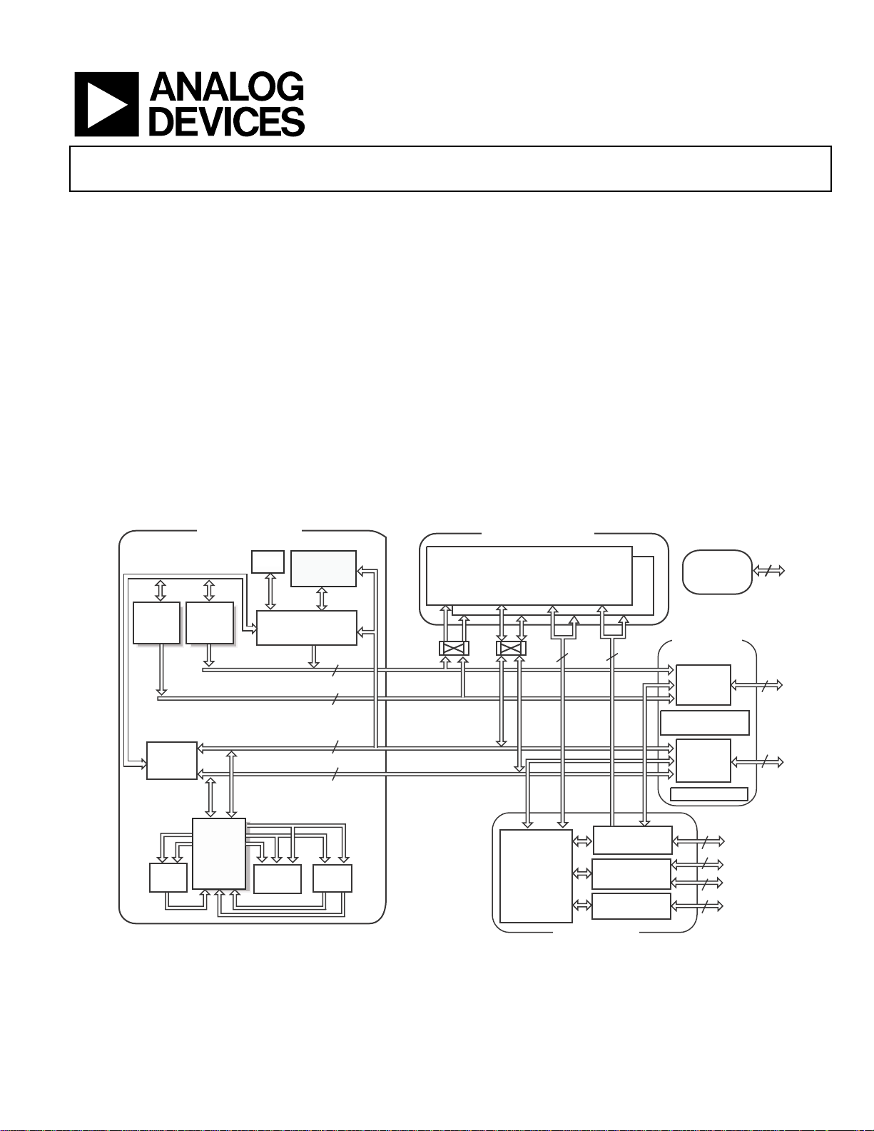
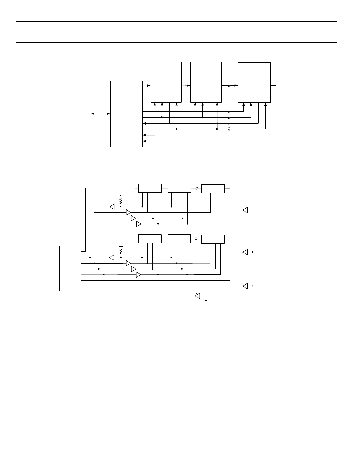
Figure 1. Functional Block Diagram
One Technology Way, P.O. Box 9106, Norwood, MA 02062-9106 U.S.A.
Tel : 781.329.4700 www.analog.com
Fax: 781.461.3113 ©2010 Analog Devices, Inc. All rights reserved.
Page 2

ADSP-21060/ADSP-21060L/ADSP-21062/ADSP-21062L/ADSP-21060C/ADSP-21060LC
PARALLEL COMPUTATIONS
Single-cycle multiply and ALU operations in parallel with
dual memory read/writes and instruction fetch
Multiply with add and subtract for accelerated FFT butterfly
computation
UP TO 4M BIT ON-CHIP SRAM
Dual-ported for independent access by core processor and
DMA
OFF-CHIP MEMORY INTERFACING
4 gigawords addressable
Programmable wait state generation, page-mode DRAM
support
DMA CONTROLLER
10 DMA channels for transfers between ADSP-2106x internal
memory and external memory, external peripherals, host
processor, serial ports, or link ports
Background DMA transfers at up to 40 MHz, in parallel with
full-speed processor execution
HOST PROCESSOR INTERFACE TO 16- AND 32-BIT MICROPROCESSORS
Host can directly read/write ADSP-2106x internal memory
and IOP registers
MULTIPROCESSING
Glueless connection for scalable DSP multiprocessing
architecture
Distributed on-chip bus arbitration for parallel bus connect
of up to six ADSP-2106xs plus host
Six link ports for point-to-point connectivity and array
multiprocessing
240 MBps transfer rate over parallel bus
240 MBps transfer rate over link ports
SERIAL PORTS
Two 40 Mbps synchronous serial ports with companding
hardware
Independent transmit and receive functions
Table 1. ADSP-2106x SHARC Processor Family Features
Feature ADSP-21060 ADSP-21062 ADSP-21060L ADSP-21062L ADSP-21060C ADSP-21060LC
SRAM 4M bits 2M bits 4M bits 2M bits 4M bits 4M bits
Operating
Voltage 5 V 5 V 3.3 V 3.3 V 5 V 3.3 V
Instruction
Rate
Package
33 MHz
40 MHz
MQFP_PQ4
PBGA
33 MHz
40 MHz
MQFP_PQ4
PBGA
33 MHz
40 MHz
MQFP_PQ4
PBGA
33 MHz
40 MHz
MQFP_PQ4
PBGA CQFP CQFP
33 MHz
40 MHz
33 MHz
40 MHz
Rev. G | Page 2 of 64 | August 2010
Page 3

ADSP-21060/ADSP-21060L/ADSP-21062/ADSP-21062L/ADSP-21060C/ADSP-21060LC
CONTENTS
Summary ............................................................... 1
Revision History ...................................................... 3
General Description ................................................. 4
SHARC Family Core Architecture ............................ 4
Memory and I/O Interface Features ........................... 5
Development Tools ............................................... 8
Evaluation Kit ...................................................... 9
Designing an Emulator-Compatible DSP Board
(Target) ........................................................... 9
Additional Information .......................................... 9
Related Signal Chains ............................................ 9
Pin Function Descriptions ........................................ 10
Target Board Connector for EZ-ICE Probe ................ 13
ADSP-21060/ADSP-21062 Specifications ..................... 15
Operating Conditions (5 V) .................................... 15
Electrical Characteristics (5 V) ................................ 15
Internal Power Dissipation (5 V) ............................. 16
REVISION HISTORY
8/10—Rev. F to Rev. G
Added new section, Related Signal Chains.......................9
Revised Table 14 ..................................................... 25
Revised Table 15 ..................................................... 26
Revised Table 28 ..................................................... 43
Clarification of Table 41 Title..................................... 54
Clarification of Table 42 Title..................................... 55
Changes to Ordering Guide ....................................... 62
External Power Dissipation (5 V) ............................ 17
ADSP-21060L/ADSP-21062L Specifications ................. 18
Operating Conditions (3.3 V) ................................. 18
Electrical Characteristics (3.3 V) ............................. 18
Internal Power Dissipation (3.3 V) .......................... 19
External Power Dissipation (3.3 V) .......................... 20
Absolute Maximum Ratings ................................... 20
ESD Caution ...................................................... 21
Package Marking Information ................................ 21
Timing Specifications ........................................... 21
Test Conditions .................................................. 48
Environmental Conditions .................................... 51
225-Ball PBGA Ball Configuration .............................. 52
240-Lead MQFP_PQ4/CQFP Pin Configuration . ........... 54
Outline Dimensions ................................................ 56
Surface-Mount Design .......................................... 61
Ordering Guide ..................................................... 62
Rev. G | Page 3 of 64 | August 2010
Page 4
ADSP-21060/ADSP-21060L/ADSP-21062/ADSP-21062L/ADSP-21060C/ADSP-21060LC
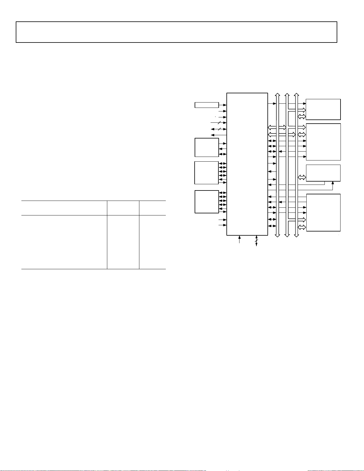
3
4
RESET JTAG
6
ADSP-2106x
BMS
1 3 CLOCK
LINK
DEVICES
(6 MAX)
(OPTIONAL)
CS
BOOT
EPROM
(OPTIONAL)
MEMO RY-
MAPPED
DEVICES
(OPTIONAL)
OE
DATA
DMA DEVICE
(OPTIONAL)
DATA
ADDR
DATA
HOST
PROCE SSOR
INTERFACE
(OPTIONAL)
CS
RD
PAGE
ADRCLK
ACK
BR1–6
DMAR1–2
CLKIN
IRQ2–0
LxCLK
TCLK0
RPBA
EBOOT
LBOOT
FLAG3–0
TIMEXP
LxACK
LxDAT3–0
DR0
DT0
RSF0
TFS0
RCLK0
TCLK1
DR1
DT1
RSF1
TFS1
RCLK1
ID2–0
SERIAL
DEVICE
(OPTIONAL)
SERIAL
DEVICE
(OPTIONAL)
PA
REDY
HBG
HBR
DMAG1–2
SBTS
MS3–0
WR
DATA47–0
DATA
ADDR
CS
ACK
WE
ADDR31–0
D
A
T
A
C
O
N
T
R
O
L
A
D
D
R
E
S
S
ADDR
GENERAL DESCRIPTION
The ADSP-2106x SHARC®—Super Harvard Architecture Computer—is a 32-bit signal processing microcomputer that offers
high levels of DSP performance. The ADSP-2106x builds on the
ADSP-21000 DSP core to form a complete system-on-a-chip,
adding a dual-ported on-chip SRAM and integrated I/O peripherals supported by a dedicated I/O bus.
Fabricated in a high speed, low power CMOS process, the
ADSP-2106x has a 25 ns instruction cycle time and operates at
40 MIPS. With its on-chip instruction cache, the processor can
execute every instruction in a single cycle. Table 2 shows performance benchmarks for the ADSP-2106x.
The ADSP-2106x SHARC represents a new standard of integration for signal computers, combining a high performance
floating-point DSP core with integrated, on-chip system features including up to 4M bit SRAM memory (see Table 1), a
host processor interface, DMA controller, serial ports and link
port, and parallel bus connectivity for glueless DSP
multiprocessing.
Table 2. Benchmarks (at 40 MHz)
Benchmark Algorithm Speed Cycles
1024 Point Complex FFT (Radix 4, with
0.46 μs 18,221
reversal)
FIR Filter (per tap) 25 ns 1
IIR Filter (per biquad) 100 ns 4
Divide (y/x) 150 ns 6
Inverse Square Root 225 ns 9
DMA Transfer Rate 240 Mbytes/s
The ADSP-2106x continues SHARC’s industry-leading standards of integration for DSPs, combining a high performance
32-bit DSP core with integrated, on-chip system features.
The block diagram on Page 1 illustrates the following architectural features:
• Computation units (ALU, multiplier and shifter) with a
shared data register file
• Data address generators (DAG1, DAG2)
• Program sequencer with instruction cache
• PM and DM buses capable of supporting four 32-bit data
transfers between memory and the core at every core processor cycle
•Interval timer
•On-chip SRAM
• External port for interfacing to off-chip memory and
peripherals
• Host port and multiprocessor Interface
• DMA controller
Rev. G | Page 4 of 64 | August 2010
• Serial ports and link ports
• JTAG Test Access Port
Figure 2. ADSP-2106x System Sample Configuration
SHARC FAMILY CORE ARCHITECTURE
The ADSP-2106x includes the following architectural features
of the ADSP-21000 family core. The ADSP-2106x processors
are code- and function-compatible with the ADSP-21020.
Independent, Parallel Computation Units
The arithmetic/logic unit (ALU), multiplier and shifter all perform single-cycle instructions. The three units are arranged in
parallel, maximizing computational throughput. Single multifunction instructions execute parallel ALU and multiplier operations. These computation units support IEEE 32-bit singleprecision floating-point, extended precision 40-bit floatingpoint, and 32-bit fixed-point data formats.
Data Register File
A general–purpose data register file is used for transferring data
between the computation units and the data buses, and for storing intermediate results. This 10-port, 32-register (16 primary,
16 secondary) register file, combined with the ADSP-21000
Harvard architecture, allows unconstrained data flow between
computation units and internal memory.
Page 5

ADSP-21060/ADSP-21060L/ADSP-21062/ADSP-21062L/ADSP-21060C/ADSP-21060LC
Single-Cycle Fetch of Instruction and Two Operands
The ADSP-2106x features an enhanced Harvard architecture in
which the data memory (DM) bus transfers data and the program memory (PM) bus transfers both instructions and data
(see Figure 1 on Page 1). With its separate program and data
memory buses and on-chip instruction cache, the processor can
simultaneously fetch two operands and an instruction (from the
cache), all in a single cycle.
Instruction Cache
The ADSP-2106x includes an on-chip instruction cache that
enables three-bus operation for fetching an instruction and two
data values. The cache is selective—only the instructions whose
fetches conflict with PM bus data accesses are cached. This
allows full-speed execution of core, looped operations such as
digital filter multiply-accumulates and FFT butterfly processing.
Data Address Generators with Hardware Circular Buffers
The ADSP-2106x’s two data address generators (DAGs) implement circular data buffers in hardware. Circular buffers allow
efficient programming of delay lines and other data structures
required in digital signal processing, and are commonly used in
digital filters and Fourier transforms. The two DAGs of the
ADSP-2106x contain sufficient registers to allow the creation of
up to 32 circular buffers (16 primary register sets, 16 secondary).
The DAGs automatically handle address pointer wraparound,
reducing overhead, increasing performance and simplifying
implementation. Circular buffers can start and end at any memory location.
Flexible Instruction Set
The 48-bit instruction word accommodates a variety of
parallel operations, for concise programming. For example, the
ADSP-2106x can conditionally execute a multiply, an add, a
subtract and a branch, all in a single instruction.
MEMORY AND I/O INTERFACE FEATURES
The ADSP-2106x processors add the following architectural
features to the SHARC family core.
Dual-Ported On-Chip Memory
The ADSP-21062/ADSP-21062L contains two megabits of onchip SRAM, and the ADSP-21060/ADSP-21060L contains
4M bits of on-chip SRAM. The internal memory is organized as
two equal sized blocks of 1M bit each for the ADSP-21062/
ADSP-21062L and two equal sized blocks of 2M bits each for
the ADSP-21060/ADSP-21060L. Each can be configured for different combinations of code and data storage. Each memory
block is dual-ported for single-cycle, independent accesses by
the core processor and I/O processor or DMA controller. The
dual-ported memory and separate on-chip buses allow two data
transfers from the core and one from I/O, all in a single cycle.
On the ADSP-21062/ADSP-21062L, the memory can be configured as a maximum of 64k words of 32-bit data, 128k words of
16-bit data, 40k words of 48-bit instructions (or 40-bit data), or
combinations of different word sizes up to two megabits. All of
the memory can be accessed as 16-bit, 32-bit, or 48-bit words.
On the ADSP-21060/ADSP-21060L, the memory can be configured as a maximum of 128k words of 32-bit data, 256k words of
16-bit data, 80k words of 48-bit instructions (or 40-bit data), or
combinations of different word sizes up to four megabits. All of
the memory can be accessed as 16-bit, 32-bit or 48-bit words.
A 16-bit floating-point storage format is supported, which effectively doubles the amount of data that can be stored on-chip.
Conversion between the 32-bit floating-point and 16-bit floating-point formats is done in a single instruction.
While each memory block can store combinations of code and
data, accesses are most efficient when one block stores data,
using the DM bus for transfers, and the other block stores
instructions and data, using the PM bus for transfers. Using the
DM bus and PM bus in this way, with one dedicated to each
memory block, assures single-cycle execution with two data
transfers. In this case, the instruction must be available in the
cache. Single-cycle execution is also maintained when one of the
data operands is transferred to or from off-chip, via the
ADSP-2106x’s external port.
On-Chip Memory and Peripherals Interface
The ADSP-2106x’s external port provides the processor’s interface to off-chip memory and peripherals. The 4-gigaword offchip address space is included in the ADSP-2106x’s unified
address space. The separate on-chip buses—for PM addresses,
PM data, DM addresses, DM data, I/O addresses, and I/O
data—are multiplexed at the external port to create an external
system bus with a single 32-bit address bus and a single 48-bit
(or 32-bit) data bus.
Addressing of external memory devices is facilitated by on-chip
decoding of high-order address lines to generate memory bank
select signals. Separate control lines are also generated for simplified addressing of page-mode DRAM. The ADSP-2106x
provides programmable memory wait states and external memory acknowledge controls to allow interfacing to DRAM and
peripherals with variable access, hold and disable time
requirements.
Host Processor Interface
The ADSP-2106x’s host interface allows easy connection to
standard microprocessor buses, both 16-bit and 32-bit, with little additional hardware required. Asynchronous transfers at
speeds up to the full clock rate of the processor are supported.
The host interface is accessed through the ADSP-2106x’s external port and is memory-mapped into the unified address space.
Four channels of DMA are available for the host interface; code
and data transfers are accomplished with low software
overhead.
The host processor requests the ADSP-2106x’s external bus with
the host bus request (HBR
(REDY) signals. The host can directly read and write the internal memory of the ADSP-2106x, and can access the DMA
channel setup and mailbox registers. Vector interrupt support is
provided for efficient execution of host commands.
), host bus grant (HBG), and ready
Rev. G | Page 5 of 64 | August 2010
Page 6
ADSP-21060/ADSP-21060L/ADSP-21062/ADSP-21062L/ADSP-21060C/ADSP-21060LC
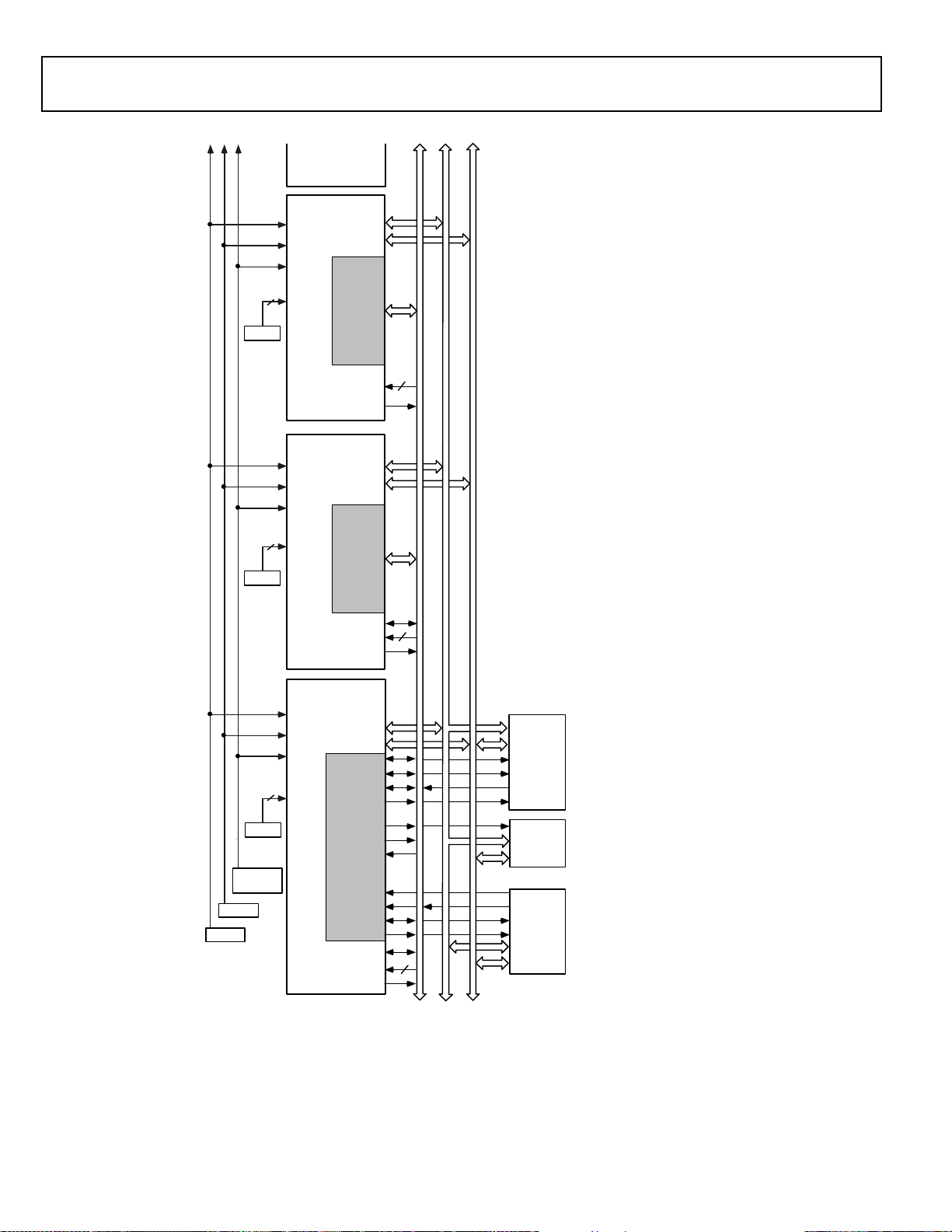
ADDR31–0
CPA
BMS
C
O
N
T
R
O
L
ADSP-2106x #1
5
CONTROL
ADSP-2106x #2
ADDR31–0
CONTROL
ADSP-2106x #3
5
ID2–0
RESET
RPBA
CLKIN
ID2–0
RESET
RPBA
ID2–0
RESET
RPBA
CLKIN
ADSP-2 106x #6
ADSP-2 106x #5
ADSP-2 106x #4
CLOCK
RESET
ADDR
DATA
HOSTPROCESSOR
INTERFACE (O PTIONAL)
ACK
GLOBAL MEMORY
AND
PERIPHERAL (O PTIONAL)
OE
ADDR
DATA
CS
ADDR
DATA
BOOT EPROM (OPTIONAL)
RDx
MS3–0
SBTS
CS
ACK
ADDR31–0
CLKIN
3
001
PAGE
3
010
3
011
BR1
BR2–6
REDY
HBG
HBR
CS
WE
WRx
5
C
O
N
T
R
O
L
A
D
D
R
E
S
S
D
A
T
A
C
O
N
T
R
O
L
A
D
D
R
E
S
S
D
A
T
A
DATA47–0
BR1–2, BR4–6
BR3
DATA47–0
BR1, BR3–6
BR2
DATA47–0
BUS
PRIORITY
CPA
Figure 3. Shared Memory Multiprocessing System
Rev. G | Page 6 of 64 | August 2010
Page 7
ADSP-21060/ADSP-21060L/ADSP-21062/ADSP-21062L/ADSP-21060C/ADSP-21060LC
0x0004 0000
0x0010 0000
0x0008 0000
0x0018 0000
0x0012 0000
0x0028 0000
0x0038 0000
0x0000 0000
0x0002 0000
0x0040 0000
BANK 1
MS0
BANK 2
MS1
BANK 3
MS2
MS3
IOP REGISTERS
SHORT WORD ADDRESSING
(16-BIT DATA WORDS)
NORMAL WORD ADDRESSING
(32-BIT DATA WORDS
48-BIT INSTRUCTION WORDS)
ADDRESS
BANK 0
SDRAM
(OPTIONAL)
0x0FFF FFFF
NONBANKED
NOTE: BANK SIZES ARE SELECTED BY
MSIZE BITS IN THE SYSCON REGISTER
0x0030 0000
INTERNAL
MEMORY
SPACE
MULTIPROCESSOR
MEMOR Y
SPACE
ADDRESS
INTERNAL MEMORY SPACE
WITH ID = 001
0x003F FFFF
EXTERNAL
MEMORY
SPACE
INTERNAL MEMORY SPACE
WITH ID = 010
INTERNAL MEMORY SPACE
WITH ID = 011
INTERNAL MEMORY SPACE
WITH ID = 100
INTERNAL MEMORY SPACE
WITH ID = 101
INTERNAL MEMORY SPACE
WITH ID = 110
BROADCASTWRITE
TO ALL ADSP-21061s
DMA Controller
The ADSP-2106x’s on-chip DMA controller allows zero-overhead data transfers without processor intervention. The DMA
controller operates independently and invisibly to the processor
core, allowing DMA operations to occur while the core is simultaneously executing its program instructions.
DMA transfers can occur between the ADSP-2106x’s internal
memory and external memory, external peripherals, or a host
processor. DMA transfers can also occur between the ADSP2106x’s internal memory and its serial ports or link ports. DMA
transfers between external memory and external peripheral
devices are another option. External bus packing to 16-,
32-, or 48-bit words is performed during DMA transfers.
Ten channels of DMA are available on the ADSP-2106x—two
via the link ports, four via the serial ports, and four via the
processor’s external port (for either host processor, other
ADSP-2106xs, memory, or I/O transfers). Four additional link
port DMA channels are shared with Serial Port 1 and the external port. Programs can be downloaded to the ADSP-2106x
using DMA transfers. Asynchronous off-chip peripherals can
control two DMA channels using DMA request/grant lines
(DMAR1–2
, DMAG1–2). Other DMA features include interrupt generation upon completion of DMA transfers and DMA
chaining for automatic linked DMA transfers.
Multiprocessing
The ADSP-2106x offers powerful features tailored to multiprocessor DSP systems. The unified address space (see Figure 4)
allows direct interprocessor accesses of each ADSP-2106x’s
internal memory. Distributed bus arbitration logic is included
on-chip for simple, glueless connection of systems containing
up to six ADSP-2106xs and a host processor. Master processor
changeover incurs only one cycle of overhead. Bus arbitration is
selectable as either fixed or rotating priority. Bus lock allows
indivisible read-modify-write sequences for semaphores. A vector interrupt is provided for interprocessor commands. Maximum throughput for interprocessor data transfer is
240M bytes/s over the link ports or external port. Broadcast
writes allow simultaneous transmission of data to all
ADSP-2106xs and can be used to implement reflective
semaphores.
Figure 4. Memory Map
Rev. G | Page 7 of 64 | August 2010
Page 8

ADSP-21060/ADSP-21060L/ADSP-21062/ADSP-21062L/ADSP-21060C/ADSP-21060LC
Link Ports
The ADSP-2106x features six 4-bit link ports that provide additional I/O capabilities. The link ports can be clocked twice per
cycle, allowing each to transfer eight bits of data per cycle. Linkport I/O is especially useful for point-to-point interprocessor
communication in multiprocessing systems.
The link ports can operate independently and simultaneously,
with a maximum data throughput of 240M bytes/s. Link port
data is packed into 32- or 48-bit words, and can be directly read
by the core processor or DMA-transferred to on-chip memory.
Each link port has its own double-buffered input and output
registers. Clock/acknowledge handshaking controls link port
transfers. Transfers are programmable as either transmit or
receive.
Program Booting
The internal memory of the ADSP-2106x can be booted at system power-up from an 8-bit EPROM, a host processor, or
through one of the link ports. Selection of the boot source is
controlled by the BMS (boot memory select), EBOOT (EPROM
Boot), and LBOOT (link/host boot) pins. 32-bit and 16-bit host
processors can be used for booting. The processor also supports a no-boot mode in which instruction execution is sourced
from the external memory.
DEVELOPMENT TOOLS
The ADSP-2106x is supported by a complete set of
CROSSCORE
Devices emulators and VisualDSP++
ment. The same emulator hardware that supports other SHARC
processors also fully emulates the ADSP-2106x.
The VisualDSP++ project management environment lets programmers develop and debug an application. This environment
includes an easy to use assembler (which is based on an algebraic syntax), an archiver (librarian/library builder), a linker, a
loader, a cycle-accurate instruction-level simulator, a C/C++
compiler, and a C/C++ runtime library that includes DSP and
mathematical functions. A key point for these tools is C/C++
code efficiency. The compiler has been developed for efficient
translation of C/C++ code to DSP assembly. The ADSP-2106x
SHARC DSP has architectural features that improve the efficiency of compiled C/C++ code.
The VisualDSP++ debugger has a number of important features. Data visualization is enhanced by a plotting package that
offers a significant level of flexibility. This graphical representation of user data enables the programmer to quickly determine
the performance of an algorithm. As algorithms grow in complexity, this capability can have increasing significance on the
designer’s development schedule, increasing productivity. Statistical profiling enables the programmer to nonintrusively poll
the processor as it is running the program. This feature, unique
to VisualDSP++, enables the software developer to passively
gather important code execution metrics without interrupting
†
CROSSCORE is a registered trademark of Analog Devices, Inc.
‡
VisualDSP++ is a registered trademark of Analog Devices, Inc.
®
†
software development tools, including Analog
®
‡
development environ-
the real-time characteristics of the program. Essentially, the
developer can identify bottlenecks in software quickly and efficiently. By using the profiler, the programmer can focus on
those areas in the program that impact performance and take
corrective action.
Debugging both C/C++ and assembly programs with the
VisualDSP++ debugger, programmers can:
• View mixed C/C++ and assembly code (interleaved source
and object information)
• Insert breakpoints
• Set conditional breakpoints on registers, memory, and
stacks
• Trace instruction execution
• Perform linear or statistical profiling of program execution
• Fill, dump, and graphically plot the contents of memory
• Perform source level debugging
• Create custom debugger windows
The VisualDSP++ IDDE lets programmers define and manage
DSP software development. Its dialog boxes and property pages
let programmers configure and manage all of the ADSP-2106x
development tools, including the color syntax highlighting in
the VisualDSP++ editor. This capability permits:
• Control in how the development tools process inputs and
generate outputs
• Maintenance of a one-to-one correspondence with the
tools’ command line switches
The VisualDSP++ kernel (VDK) incorporates scheduling and
resource management tailored specifically to address the memory and timing constraints of DSP programming. These
capabilities enable engineers to develop code more effectively,
eliminating the need to start from the very beginning when
developing new application code. The VDK features include
threads, critical and unscheduled regions, semaphores, events,
and device flags. The VDK also supports priority-based, preemptive, cooperative, and time-sliced scheduling approaches. In
addition, the VDK was designed to be scalable. If the application
does not use a specific feature, the support code for that feature
is excluded from the target system.
Because the VDK is a library, a developer can decide whether to
use it or not. The VDK is integrated into the VisualDSP++
development environment, but can also be used via standard
command line tools. When the VDK is used, the development
environment assists the developer with many error-prone tasks
and assists in managing system resources, automating the generation of various VDK-based objects, and visualizing the
system state, when debugging an application that uses the VDK.
Use the expert linker to visually manipulate the placement of
code and data on the embedded system. View memory utilization in a color-coded graphical form, easily move code and data
to different areas of the DSP or external memory with a drag of
the mouse, and examine run-time stack and heap usage. The
Rev. G | Page 8 of 64 | August 2010
Page 9

ADSP-21060/ADSP-21060L/ADSP-21062/ADSP-21062L/ADSP-21060C/ADSP-21060LC
expert linker is fully compatible with existing linker definition
file (LDF), allowing the developer to move between the graphical and textual environments.
In addition to the software development tools available from
Analog Devices, third parties provide a wide range of tools supporting the SHARC processor family. Third party software tools
include DSP libraries, real-time operating systems, and block
diagram design tools.
EVALUATION KIT
®
Analog Devices offers a range of EZ-KIT Lite
forms to use as a cost-effective method to learn more about
developing or prototyping applications with Analog Devices
processors, platforms, and software tools. Each EZ-KIT Lite
includes an evaluation board along with an evaluation suite of
the VisualDSP++ development and debugging environment
with the C/C++ compiler, assembler, and linker. Also included
are sample application programs, power supply, and a USB
cable. All evaluation versions of the software tools are limited
for use only with the EZ-KIT Lite product.
The USB controller on the EZ-KIT Lite board connects the
board to the USB port of the user’s PC, enabling the
VisualDSP++ evaluation suite to emulate the on-board processor in-circuit. This permits the customer to download, execute,
and debug programs for the EZ-KIT Lite system. It also allows
in-circuit programming of the on-board flash device to store
user-specific boot code, enabling the board to run as a standalone unit, without being connected to the PC.
With a full version of VisualDSP++ installed (sold separately),
engineers can develop software for the EZ-KIT Lite or any custom-defined system. Connecting an Analog Devices JTAG
emulator to the EZ-KIT Lite board enables high speed, nonintrusive emulation.
†
evaluation plat-
Reference on the Analog Devices website (www.analog.com)—
use site search on “EE-68.” This document is updated regularly
to keep pace with improvements to emulator support.
ADDITIONAL INFORMATION
This data sheet provides a general overview of the ADSP-2106x
architecture and functionality. For detailed information on the
ADSP-21000 family core architecture and instruction set, refer
to the ADSP-2106x SHARC User’s Manual, Revision 2.1.
RELATED SIGNAL CHAINS
A signal chain is a series of signal-conditioning electronic components that receive input (data acquired from sampling either
real-time phenomena or from stored data) in tandem, with the
output of one portion of the chain supplying input to the next.
Signal chains are often used in signal processing applications to
gather and process data or to apply system controls based on
analysis of real-time phenomena. For more information about
this term and related topics, see the “signal chain” entry in the
Glossary of EE Terms on the Analog Devices website.
Analog Devices eases signal processing system development by
providing signal processing components that are designed to
work together well. A tool for viewing relationships between
specific applications and related components is available on the
www.analog.com website.
The Application Signal Chains page in the Circuits from the
TM
Lab
site (http://www.analog.com/signalchains) provides:
• Graphical circuit block diagram presentation of signal
chains for a variety of circuit types and applications
• Drill down links for components in each chain to selection
guides and application information
• Reference designs applying best practice design techniques
DESIGNING AN EMULATOR-COMPATIBLE DSP BOARD (TARGET)
The Analog Devices family of emulators are tools that every
DSP developer needs to test and debug hardware and software
systems. Analog Devices has supplied an IEEE 1149.1 JTAG test
access port (TAP) on each JTAG DSP. Nonintrusive in-circuit
emulation is assured by the use of the processor’s JTAG interface—the emulator does not affect target system loading or timing. The emulator uses the TAP to access the internal features of
the DSP, allowing the developer to load code, set breakpoints,
observe variables, observe memory, and examine registers. The
DSP must be halted to send data and commands, but once an
operation has been completed by the emulator, the DSP system
is set running at full speed with no impact on system timing.
To use these emulators, the target board must include a header
that connects the DSP’s JTAG port to the emulator.
For details on target board design issues including mechanical
layout, single processor connections, multiprocessor scan
chains, signal buffering, signal termination, and emulator pod
logic, see the EE-68: Analog Devices JTAG Emulation Technical
†
EZ-KIT Lite is a registered trademark of Analog Devices, Inc.
Rev. G | Page 9 of 64 | August 2010
Page 10
ADSP-21060/ADSP-21060L/ADSP-21062/ADSP-21062L/ADSP-21060C/ADSP-21060LC
PIN FUNCTION DESCRIPTIONS
The ADSP-2106x pin definitions are listed below. Inputs identified as synchronous (S) must meet timing requirements with
respect to CLKIN (or with respect to TCK for TMS, TDI).
Inputs identified as asynchronous (A) can be asserted asynchronously to CLKIN (or to TCK for TRST
).
Unused inputs should be tied or pulled to VDD or GND, except
for ADDR31–0, DATA47–0, FLAG3–0, and inputs that have
internal pull-up or pull-down resistors (CPA
, ACK, DTx, DRx,
TCLKx, RCLKx, LxDAT3–0, LxCLK, LxACK, TMS, and
TDI)—these pins can be left floating. These pins have a
logic-level hold circuit that prevents the input from floating
internally.
Table 3. Pin Descriptions
Pin Type Function
ADDR31–0 I/O/T External Bus Address. The ADSP-2106x outputs addresses for external memory and peripherals on these
pins. In a multiprocessor system, the bus master outputs addresses for read/write of the internal memory
or IOP registers of other ADSP-2106xs. The ADSP-2106x inputs addresses when a host processor or multiprocessing bus master is reading or writing its internal memory or IOP registers.
DATA47–0 I/O/T External Bus Data. The ADSP-2106x inputs and outputs data and instructions on these pins. 32-bit single-
precision floating-point data and 32-bit fixed-point data is transferred over bits 47–16 of the bus. 40-bit
extended-precision floating-point data is transferred over bits 47–8 of the bus. 16-bit short word data is
transferred over bits 31–16 of the bus. In PROM boot mode, 8-bit data is transferred over bits 23–16. Pull-up
resistors on unused DATA pins are not necessary.
MS3–0
RD I/O/T Memory Read Strobe. This pin is asser ted (low) when the ADSP-2106x reads from external memory devices
WR
PAG E O /T DRAM Page Boundary. The ADSP-2106x asserts this pin to signal that an external DRAM page boundary
ADRCLK O/T Clock Output Reference. In a multiprocessing system, ADRCLK is output by the bus master.
SW
A = Asynchronous, G = Ground, I = Input, O = Output, P = Power Supply, S = Synchronous, (A/D) = Active Drive, (O/D) = Open Drain,
T = Three-State (when SBTS is asserted, or when the ADSP-2106x is a bus slave)
O/T Memory Select Lines. These lines are asserted (low) as chip selects for the corresponding banks of external
memory. Memory bank size must be defined in the ADSP-2106x’s system control register (SYSCON). The
MS3–0 lines are decoded memory address lines that change at the same time as the other address lines.
When no external memory access is occurring, the MS3–0
a conditional memory access instruction is executed, whether or not the condition is true. MS0 can be used
with the PAGE signal to implement a bank of DR AM memory (Bank 0). In a multiprocessing system the MS3–0
lines are output by the bus master.
or from the internal memory of other ADSP-2106xs. External devices (including other ADSP-2106xs) must
assert RD to read from the ADSP-2106x’s internal memory. In a multiprocessing system, RD is output by the
bus master and is input by all other ADSP-2106xs.
I/O/T Memory Write Strobe. This pin is asserted (low) when the ADSP-2106x wri tes to external memory devices
or to the internal memory of other ADSP-2106xs. External devices must assert WR
2106x’s internal memory. In a multiprocessing system, WR is output by the bus master and is input by all
other ADSP-2106xs.
has been crossed. DRAM page size must be defined in the ADSP-2106x’s memory control register (WAIT).
DRAM can only be implemented in external memory Bank 0; the PAGE signal can only be activated for Bank
0 accesses. In a multiprocessing system, PAGE is output by the bus master
I/O/T Synchronous Write Select. T hi s si g na l i s u s ed t o interface the ADSP-2106x to synchronous memory devices
(including other ADSP-2106xs). The ADSP-2106x asserts SW
impending write cycle, which can be aborted if WR
instruction). In a multiprocessing system, SW is output by the bus master and is input by all other
ADSP-2106xs to determine if the multiprocessor memory access is a read or write. SW
time as the address output. A host processor using synchronous writes must assert this pin when writing to
the ADSP-2106x(s).
lines are inactive; they are active however when
to write to the ADSP-
(low) to provide an early indication of an
is not later asserted (e.g., in a conditional write
is asserted at the same
Rev. G | Page 10 of 64 | August 2010
Page 11
ADSP-21060/ADSP-21060L/ADSP-21062/ADSP-21062L/ADSP-21060C/ADSP-21060LC
Table 3. Pin Descriptions (Continued)
Pin Type Function
ACK I/O/S Memory Acknowledge. External devices can deassert ACK (low) to add wait states to an external memory
access. ACK is used by I/O devices, memory controllers, or other peripherals to hold off completion of an
external memory access. The ADSP-2106x deasserts ACK as an output to add waitstates to a synchronous
access of its internal memory. In a multiprocessing system, a slave ADSP-2106x deasserts the bus master’s
ACK input to add wait state(s) to an access of its internal memory. The bus master has a keeper latch on its
ACK pin that maintains the input at the level to which it was last driven.
SBTS
IRQ2–0
FLAG3–0 I/O/A Flag Pins. Each is configured via control bits as either an input or output. As an input, they can be tested as
TIMEXP O Timer Expired. Asserted for four cycles when the timer is enabled and TCOUNT decrements to zero.
HBR
HBG
CS
REDY O (O/D) Host Bus Acknowledge. The ADSP-2106x deasserts REDY (low) to add wait states to an asynchronous access
DMAR2–1
DMAG2–1
BR6–1
ID2–0
RPBA I/S Rotating Priority Bus Arbitration Select. When RPBA is high, rotating priority for multiprocessor bus
CPA
DTx O Data Transmit (Serial Ports 0, 1). Each DT pin has a 50 kΩ internal pull-up resistor.
DRx I Data Receive (Serial Ports 0, 1). Each DR pin has a 50 kΩ internal pull-up resistor.
TCLKx I/O Transmit Clock (Serial Ports 0, 1). Each TCLK pin has a 50 kΩ internal pull-up resistor.
RCLKx I/O Receive Clock (Serial Ports 0, 1). Each RCLK pin has a 50 kΩ internal pull-up resistor.
A = Asynchronous, G = Ground, I = Input, O = Output, P = Power Supply, S = Synchronous, (A/D) = Active Drive, (O/D) = Open Drain,
T = Three-State (when SBTS is asserted, or when the ADSP-2106x is a bus slave)
I/S Suspend Bus Three-State. External devices can assert SBTS (low) to place the external bus address, data,
selects, and strobes in a high impedance state for the following cycle. If the ADSP-2106x attempts to access
external memory while SBTS is asserted, the processor will halt and the memory access will not be completed
until SBTS
or used with a DRAM controller.
I/A Interrupt Request Lines. May be either edge-triggered or level-sensitive.
a condition. As an output, they can be used to signal external peripherals.
I/A Host Bus Request. This pin must be asserted by a host processor to request control of the ADSP-2106x’s
external bus. When HBR
relinquish the bus and assert HBG. To relinquish the bus, the ADSP-2106x places the address, data, select
and strobe lines in a high impedance state. HBR
multiprocessing system.
I/O Host Bus Grant. Acknowledges a bus request, indicating that the host processor may take control of the
external bus. HBG is asser ted (held low) by the ADSP-2106x until HBR is released. In a multiprocessing system,
HBG
I/A Chip Select. Asserted by host processor to select the ADSP-2106x.
of its internal memory or IOP registers by a host. This pin is an open-drain output (O/D) by default; it can be
programmed in the ADREDY bit of the SYSCON register to be active drive (A/D). REDY will only be output if
the CS
I/A DMA Request 1 (DMA Channel 7) and DMA Request 2 (DMA Channel 8).
O/T DMA Grant 1 (DMA Channel 7) and DMA Grant 2 (DMA Channel 8).
I/O/S Multiprocessing Bus Requests. Used by multiprocessing ADSP-2106xs to arbitrate for bus master-ship. An
ADSP-2106x only drives its own BR
others. In a multiprocessor system with less than six ADSP-2106xs, the unused BR
high; the processor’s own BRx line must not be pulled high or low because it is an output.
O (O/D) Multiprocessing ID. Determines which multiprocessing bus request (BR1– BR6) is used by ADSP-2106x.
ID = 001 corresponds to BR1, ID = 010 corresponds to BR2, etc. ID = 000 in single-processor systems. These
lines are a system configuration selection that should be hardwired or changed at reset only.
arbitration is selected. When RPBA is low, fixed priority is selected. This signal is a system configuration
selection that must be set to the same value on every ADSP-2106x. If the value of RPBA is changed during
system operation, it must be changed in the same CLKIN cycle on every ADSP-2106x.
I/O (O/D) Core Priority Access. Asserting its CPA pin allows the core processor of an ADSP-2106x bus slave to interrupt
background DMA transfers and gain access to the external bus. CPA
to all ADSP-2106xs in the system. The CPA
not required in a system, the CPA pin should be left unconnected.
is deasserted. SBTS should only be used to recover from host processor/ADSP-2106x deadlock,
is asserted in a multiprocessing system, the ADSP-2106x that is bus master will
has priority over all ADSP-2106x bus requests BR6–1 in a
is output by the ADSP-2106x bus master and is monitored by all others.
and HBR inputs are asserted.
x line (corresponding to the value of its ID2-0 inputs) and monitors all
x pins should be pulled
is an open drain output that is connected
pin has an internal 5 kΩ pull-up resistor. If core access priority is
Rev. G | Page 11 of 64 | August 2010
Page 12
ADSP-21060/ADSP-21060L/ADSP-21062/ADSP-21062L/ADSP-21060C/ADSP-21060LC
Table 3. Pin Descriptions (Continued)
Pin Type Function
TFSx I/O Transmit Frame Sync (Serial Ports 0, 1).
RFSx I/O Receive Frame Sync (Serial Ports 0, 1).
LxDAT3–0 I/O Link Port Data (Link Ports 0–5). Each LxDAT pin has a 50 kΩ internal pull-down resistor that is enabled or
disabled by the LPDRD bit of the LCOM register.
LxCLK I/O Link Port Clock (Link Ports 0–5). Each LxCLK pin has a 50 kΩ internal pull-down resistor that is enabled or
disabled by the LPDRD bit of the LCOM register.
LxACK I/O Link Port Acknowledge (Link Ports 0–5). Each LxACK pin has a 50 kΩ internal pull-down resistor that is
enabled or disabled by the LPDRD bit of the LCOM register.
EBOOT I EPROM Boot Select. When EBOOT is high, the ADSP-2106x is configured for booting from an 8-bit EPROM.
When EBOOT is low, the LBOOT and BMS
description below. This signal is a system configuration selection that should be hardwired.
LBOOT I Link Boot. When LBOOT is high, the ADSP-2106x is configured for link port booting. When LBOOT is low,
the ADSP-2106x is configured for host processor booting or no booting. See the table in the BMS
description below. This signal is a system configuration selection that should be hardwired.
BMS
CLKIN I Clock In. External clock input to the ADSP-2106x. The instruction cycle rate is equal to CLKIN. CLKIN should
RESET I/A Processor Reset. Resets the ADSP-2106x to a known state and begins program execution at the program
TCK I Test Clock (JTAG). Provides an asynchronous clock for JTAG boundary scan.
TMS I/S Test Mode Select (JTAG). Used to control the test state machine. TMS has a 20 kΩ internal pull-up resistor.
TDI I/S Test Data Input (JTAG). Provides serial data for the boundary scan logic. TDI has a 20 kΩ internal pull-up
TDO O Test Data Output (JTAG). Serial scan output of the boundary scan path.
TRST
EMU
ICSA O Reserved, leave unconnected.
VDD P Power Supply; nominally 5.0 V dc for 5 V devices or 3.3 V dc for 3.3 V devices. (30 pins).
GND G Power Supply Return. (30 pins).
NC Do Not Connect. Reserved pins which must be left open and unconnected.
A = Asynchronous, G = Ground, I = Input, O = Output, P = Power Supply, S = Synchronous, (A/D) = Active Drive, (O/D) = Open Drain,
T = Three-State (when SBTS
I/OT Boot Memory Select. Output: Used as chip select for boot EPROM devices (when EBOOT = 1, LBOOT = 0).
In a multiprocessor system, BMS
occur and that ADSP-2106x will begin executing instructions from external memory. See table below. This
input is a system configuration selection that should be hardwired. *Three-statable only in EPROM boot
mode (when BMS
EBOOT LBOOT BMS
1 0 Output EPROM (Connect BMS to EPROM chip select.)
0 0 1 (Input) Host Processor
0 1 1 (Input) Link Port
0 0 0 (Input) No Booting. Processor executes from external memory.
010 (Input) Reserved
1 1 x (Input) Reserved
not be halted, changed, or operated below the minimum specified frequency.
memory location specified by the hardware reset vector address. This input must be asserted (low) at
power-up.
resistor.
I/A Test Reset (JTAG). Resets the test state machine. TRST must be asser ted (pulsed low) after power-up or held
low for proper operation of the ADSP-2106x. TRST
O Emulation Status. Must be connected to the ADSP-2106x EZ-ICE target board connector only.
is asserted, or when the ADSP-2106x is a bus slave)
is an output).
is output by the bus master. Input: When low, indicates that no booting will
inputs determine booting mode. See the table in the BMS pin
pin
Booting Mode
has a 20 kΩ internal pull-up resistor.
Rev. G | Page 12 of 64 | August 2010
Page 13
ADSP-21060/ADSP-21060L/ADSP-21062/ADSP-21062L/ADSP-21060C/ADSP-21060LC
TOP VIE W
13 14
11 12
910
9
7 8
56
3 4
12
EMU
GND
TMS
TCK
TRST
TDI
TDO
GND
KEY (NO PIN)
BTMS
BTCK
BTRST
BTDI
GND
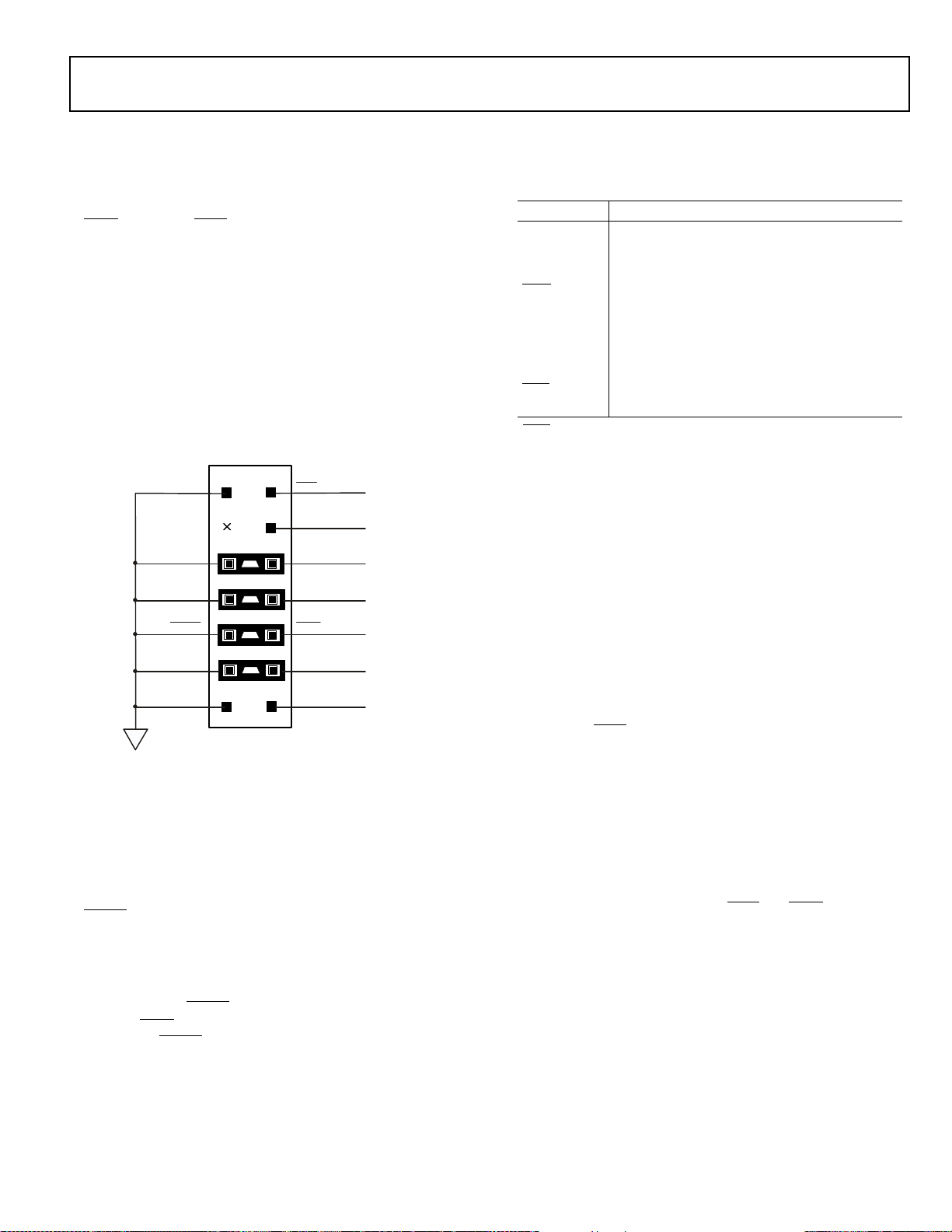
TARGET BOARD CONNECTOR FOR EZ-ICE PROBE
The ADSP-2106x EZ-ICE® Emulator uses the IEEE
1149.1JTAG test access port of the ADSP-2106x to monitor and
control the target board processor during emulation. The
EZ-ICE probe requires the ADSP-2106x’s CLKIN, TMS, TCK,
TRST
, TDI, TDO, EMU, and GND signals be made accessible
on the target system via a 14-pin connector (a 2-row 7-pin strip
header) such as that shown in Figure 5. The EZ-ICE probe plugs
directly onto this connector for chip-on-board emulation. You
must add this connector to your target board design if you
intend to use the ADSP-2106x EZ-ICE. The total trace length
between the EZ-ICE connector and the furthest device sharing
the EZ-ICE JTAG pin should be limited to 15 inches maximum
for guaranteed operation. This length restriction must include
EZ-ICE JTAG signals that are routed to one or more
ADSP-2106x devices, or a combination of ADSP-2106x devices
and other JTAG devices on the chain.
Figure 5. Target Board Connector for ADSP-2106x EZ-ICE Emulator
(Jumpers in Place)
The 14-pin, 2-row pin strip header is keyed at the Pin 3 location—Pin 3 must be removed from the header. The pins must be
0.025 inch square and at least 0.20 inch in length. Pin spacing
should be 0.1 × 0.1 inches. Pin strip headers are available from
vendors such as 3M, McKenzie, and Samtec. The BTMS, BTCK,
BTRST
, and BTDI signals are provided so that the test access
port can also be used for board-level testing.
When the connector is not being used for emulation, place
jumpers between the Bxxx pins and the xxx pins as shown in
Figure 5. If you are not going to use the test access port for
board testing, tie BTRST
V
. The TRST pin must be asserted (pulsed low) after power-
DD
up (through BTRST
operation of the ADSP-2106x. None of the Bxxx pins (Pins 5, 7,
9, and 11) are connected on the EZ-ICE probe.
to GND and tie or pull up BTCK to
on the connector) or held low for proper
Rev. G | Page 13 of 64 | August 2010
The JTAG signals are terminated on the EZ-ICE probe as shown
in Table 4.
Table 4. Core Instruction Rate/CLKIN Ratio Selection
Signal Termination
TMS Driven Through 22 Ω Resistor (16 mA Driver)
TCK Driven at 10 MHz Through 22 Ω Resistor (16 mA
Driver)
1
TRST
Active Low Driven Through 22 Ω Resistor (16 mA
Driver) (Pulled-Up by On-Chip 20 kΩ Resistor)
TDI Driven by 22 Ω Resistor (16 mA Driver)
TDO One TTL Load, Split Termination (160/220)
CLKIN One TTL Load, Split Termination (160/220)
EMU
Active Low 4.7 kΩ Pull-Up Resistor, One TTL Load
(Open-Drain Output from the DSP)
1
TRST is driven low until the EZ-ICE probe is turned on by the emulator at software
start-up. After software start-up, is driven high.
Figure 6 shows JTAG scan path connections for systems that
contain multiple ADSP-2106x processors.
Connecting CLKIN to Pin 4 of the EZ-ICE header is optional.
The emulator only uses CLKIN when directed to perform operations such as starting, stopping, and single-stepping multiple
ADSP-2106xs in a synchronous manner. If you do not need
these operations to occur synchronously on the multiple processors, simply tie Pin 4 of the EZ-ICE header to ground.
If synchronous multiprocessor operations are needed and
CLKIN is connected, clock skew between the multiple
ADSP-2106x processors and the CLKIN pin on the EZ-ICE
header must be minimal. If the skew is too large, synchronous
operations may be off by one or more cycles between processors. For synchronous multiprocessor operation TCK, TMS,
CLKIN, and EMU
should be treated as critical signals in terms
of skew, and should be laid out as short as possible on your
board. If TCK, TMS, and CLKIN are driving a large number of
ADSP-2106xs (more than eight) in your system, then treat them
as a “clock tree” using multiple drivers to minimize skew. (See
Figure 7 and “JTAG Clock Tree” and “Clock Distribution” in
the “High Frequency Design Considerations” section of the
ADSP-2106x User’s Manual, Revision 2.1.)
If synchronous multiprocessor operations are not needed (i.e.,
CLKIN is not connected), just use appropriate parallel termination on TCK and TMS. TDI, TDO, EMU
and TRST are not
critical signals in terms of skew.
For complete information on the SHARC EZ-ICE, see the
ADSP-21000 Family JTAG EZ-ICE User's Guide and Reference.
Page 14
ADSP-21060/ADSP-21060L/ADSP-21062/ADSP-21062L/ADSP-21060C/ADSP-21060LC
T
R
S
T
E
M
U
T
R
S
T
ADSP-21 06x
#1
JTA G
DEVICE
(OPTIONAL)
ADSP-2106x
n
TDI
EZ-ICE
JTAG
CONNECTOR
OTHER
JTAG
CONTROLLER
OPTION AL
T
C
K
T
M
S
EMU
TMS
TCK
TDO
CLKIN
TRST
T
C
K
T
M
S
T
C
K
T
M
S
TDI
TDO
TDI
TDO TDO
TDI
T
R
S
T
T
R
S
T
E
M
U
E
M
U
SYSTEM
CLKIN
EMU
5kV
*
TDI TDO
5kV
TDI
EMU
TMS
TCK
TDO
TRST
CLKIN
*OPEN-DRAIN DRIVER OR EQUIVALENT, i.e.,
TDI TDO
TDI TDO
TDI TDO TDI TDO
TDI TDO
*
Figure 6. JTAG Scan Path Connections for Multiple ADSP-2106x Systems
Figure 7. JTAG Clocktree for Multiple ADSP-2106x Systems
Rev. G | Page 14 of 64 | August 2010
Page 15
ADSP-21060/ADSP-21060L/ADSP-21062/ADSP-21062L/ADSP-21060C/ADSP-21060LC
ADSP-21060/ADSP-21062 SPECIFICATIONS
Note that component specifications are subject to change
without notice.
OPERATING CONDITIONS (5 V)
A Grade C Grade K Grade
Parameter Description Min Max Min Max Min Max Unit
V
DD
T
CASE
1
1
V
IH
2
V
2
IH
2
1,
V
IL
1
Applies to input and bidirectional pins: DATA47–0, ADDR31–0, RD, WR, SW, ACK, SBTS, IRQ2–0, FLAG3–0, HGB, CS, DMAR1, DMAR2, BR6–1, ID2–0, RPBA, CPA, TFS0,
TFS1, RFS0, RFS1, LxDAT3–0, LxCLK, LxACK, EBOOT, LBOOT, BMS, TMS, TDI, TCK, HBR, DR0, DR1, TCLK0, TCLK1, RCLK0, RCLK1.
2
Applies to input pins: CLKIN, RESET, TRST.
ELECTRICAL CHARACTERISTICS (5 V)
Parameter Description Test Conditions Min Max Unit
1, 2
V
OH
1, 2
V
OL
3, 4
I
IH
3
I
IL
4
I
ILP
5, 6, 7, 8
I
OZH
5, 9
I
OZL
9
I
OZHP
7
I
OZLC
10
I
OZLA
8
I
OZLAR
6
I
OZLS
11, 12
C
IN
1
Applies to output and bidirectional pins: DATA47–0, ADDR31-0, MS3–0, RD, WR, PAGE, ADRCLK, SW, ACK, FLAG3–0, TIMEXP, HBG, REDY, DMAG1, DMAG2,
, CPA, DT0, DT1, TCLK0, TCLK1, RCLK0, RCLK1, TFS0, TFS1, RFS0, RFS1, LxDAT3–0, LxCLK, LxACK, BMS, TDO, EMU, ICSA.
BR6–1
2
See “Output Drive Currents” for typical drive current capabilities.
3
Applies to input pins: ACK, SBTS, IRQ2–0, HBR, CS, DMAR1, DMAR2, ID2–0, RPBA, EBOOT, LBOOT, CLKIN, RESET, TCK.
4
Applies to input pins with internal pull-ups: DR0, DR1, TRST, TMS, TDI.
5
Applies to three-statable pins: DATA47–0, ADDR31–0, MS3–0, RD, WR, PAGE, ADRCLK, SW, ACK, FLAG3–0, HBG, REDY, DMAG1, DMAG2, BMS, BR6–1, TFSx, RFSx,
TDO, EMU
mastership.)
6
Applies to three-statable pins with internal pull-ups: DT0, DT1, TCLK0, TCLK1, RCLK0, RCLK1.
7
Applies to CPA pin.
8
Applies to ACK pin when pulled up. (Note that ACK is pulled up internally with 2 kΩ during reset in a multiprocessor system, when ID2–0 = 001 and another ADSP-2106xL
is not requesting bus mastership).
9
Applies to three-statable pins with internal pull-downs: LxDAT3–0, LxCLK, LxACK.
10
Applies to ACK pin when keeper latch enabled.
11
Applies to all signal pins.
12
Guaranteed but not tested.
Supply Voltage 4.75 5.25 4.75 5.25 4.75 5.25 V
Case Operating Temperature –40 +85 –40 +100 –40 +85 °C
High Level Input Voltage @ VDD = Max 2.0 VDD + 0.5 2.0 VDD + 0.5 2.0 VDD + 0.5 V
High Level Input Voltage @ VDD = Max 2.2 VDD + 0.5 2.2 VDD + 0.5 2.2 VDD + 0.5 V
Low Level Input Voltage @ VDD = Min –0.5 +0.8 –0.5 +0.8 –0.5 +0.8 V
High Level Output Voltage @ VDD = Min, IOH = –2.0 mA 4.1 V
Low Level Output Voltage @ VDD = Min, IOL = 4.0 mA 0.4 V
High Level Input Current @ VDD = Max, VIN = VDD Max 10 μA
Low Level Input Current @ VDD = Max, VIN = 0 V 10 μA
Low Level Input Current @ VDD = Max, VIN = 0 V 150 μA
Three-State Leakage Current @ VDD = Max, VIN = VDD Max 10 μA
Three-State Leakage Current @ VDD = Max, VIN = 0 V 10 μA
Three-State Leakage Current @ VDD = Max, VIN = VDD Max 350 μA
Three-State Leakage Current @ VDD = Max, VIN = 0 V 1.5 mA
Three-State Leakage Current @ VDD = Max, VIN = 1.5 V 350 μA
Three-State Leakage Current @ VDD = Max, VIN = 0 V 4.2 mA
Three-State Leakage Current @ VDD = Max, VIN = 0 V 150 μA
Input Capacitance fIN = 1 MHz, T
. (Note that ACK is pulled up internally with 2 kΩ during reset in a multiprocessor system, when ID2–0 = 001 and another ADSP-2106x is not requesting bus
= 25°C, VIN = 2.5 V 4.7 pF
CASE
Rev. G | Page 15 of 64 | August 2010
Page 16

ADSP-21060/ADSP-21060L/ADSP-21062/ADSP-21062L/ADSP-21060C/ADSP-21060LC
INTERNAL POWER DISSIPATION (5 V)
These specifications apply to the internal power portion of VDD
only. For a complete discussion of the code used to measure
power dissipation, see the technical note “SHARC Power Dissipation Measurements.”
Specifications are based on the operating scenarios.
Operation Peak Activity (I
DDINPEAK
) High Activity (I
DDINHIGH
) Low Activity (I
Instruction Type Multifunction Multifunction Single Function
Instruction Fetch Cache Internal Memory Internal Memory
Core memory Access 2 Per Cycle (DM and PM) 1 Per Cycle (DM) None
Internal Memory DMA 1 Per Cycle 1 Per 2 Cycles 1 Per 2 Cycles
To estimate power consumption for a specific application, use
the following equation where% is the amount of time your program spends in that state:
%PEAK I
%IDLE I
+%HIGH I
DDINPEAK
= Power Consumption
DDIDLE
DDINHIGH
+%LOW I
DDINLOW
+
Parameter Test Conditions Max Units
3
DDINPEAK
1
2
2
tCK = 30 ns, VDD = Max
= 25 ns, VDD = Max
t
CK
tCK = 30 ns, VDD = Max
= 25 ns, VDD = Max
t
CK
tCK = 30 ns, VDD = Max
tCK = 25 ns, VDD = Max
745
850
575
670
340
390
mA
mA
mA
mA
mA
mA
VDD = Max 200 mA
represents worst case processor operation and is not sustainable under normal application conditions. Actual internal power
is a composite average based on a range of low activity code.
DDINLOW
I
I
I
I
1
The test program used to measure I
2
I
3
Idle denotes ADSP-2106x state during execution of IDLE instruction.
Supply Current (Internal)
DDINPEAK
Supply Current (Internal)
DDINHIGH
Supply Current (Internal)
DDINLOW
Supply Current (Idle)
DDIDLE
measurements made using typical applications are less than specified.
is a composite average based on a range of high activity code. I
DDINHIGH
DDINLOW
)
Rev. G | Page 16 of 64 | August 2010
Page 17

ADSP-21060/ADSP-21060L/ADSP-21062/ADSP-21062L/ADSP-21060C/ADSP-21060LC
EXTERNAL POWER DISSIPATION (5 V)
Total power dissipation has two components, one due to internal circuitry and one due to the switching of external output
drivers. Internal power dissipation is dependent on the instruction execution sequence and the data operands involved.
Internal power dissipation is calculated in the following way:
P
= I
INT
The external component of total power dissipation is caused by
the switching of output pins. Its magnitude depends on:
• the number of output pins that switch during each cycle
(O)
• the maximum frequency at which they can switch (f)
• their load capacitance (C)
• their voltage swing (V
and is calculated by:
P
EXT
The load capacitance should include the processor’s package
capacitance (CIN). The switching frequency includes driving
the load high and then back low. Address and data pins can
× V
DDIN
= O × C × V
DD
DD
2
× f
DD
)
drive high and low at a maximum rate of 1/(2t
strobe can switch every cycle at a frequency of 1/t
switch at 1/(2t
Example: Estimate P
), but selects can switch on each cycle.
CK
with the following assumptions:
EXT
• A system with one bank of external data memory RAM
(32-bit)
• Four 128K × 8 RAM chips are used, each with a load of
10 pF
• External data memory writes occur every other cycle, a rate
of 1/(4t
), with 50% of the pins switching
CK
• The instruction cycle rate is 40 MHz (t
The P
equation is calculated for each class of pins that can
EXT
drive:
A typical power consumption can now be calculated for these
conditions by adding a typical internal power dissipation:
P
= P
TOTAL
EXT
+ (I
DDIN
× 5.0 V)
2
Note that the conditions causing a worst-case P
from those causing a worst-case P
. Maximum P
INT
occur while 100% of the output pins are switching from all ones
to all zeros. Note also that it is not common for an application to
). The write
CK
= 25 ns)
CK
EXT
have 100% or even 50% of the outputs switching
simultaneously.
Table 5. External Power Calculations (5 V Devices)
Pin Type No. of Pins % Switching × C × f × V
DD
2
= P
EXT
Address 15 50 × 44.7 pF × 10 MHz × 25 V = 0.084 W
MS0
WR
10 × 44.7 pF × 10 MHz × 25 V = 0.000 W
1– × 44.7 pF × 20 MHz × 25 V = 0.022 W
Data 32 50 × 14.7 pF × 10 MHz × 25 V = 0.059 W
ADDRCLK 1 – × 4.7 pF × 20 MHz × 25 V = 0.002 W
. Select pins
CK
are different
cannot
INT
P
= 0.167 W
EXT
Rev. G | Page 17 of 64 | August 2010
Page 18
ADSP-21060/ADSP-21060L/ADSP-21062/ADSP-21062L/ADSP-21060C/ADSP-21060LC
ADSP-21060L/ADSP-21062L SPECIFICATIONS
Note that component specifications are subject to change
without notice.
OPERATING CONDITIONS (3.3 V)
A Grade C Grade K Grade
Parameter Description Min Max Min Max Min Max Unit
V
DD
T
CASE
1
1
V
IH
2
V
2
IH
2
1,
V
IL
1
Applies to input and bidirectional pins: DATA47–0, ADDR31–0, RD, WR, SW, ACK, SBTS, IRQ2–0, FLAG3–0, HGB, CS, DMAR1, DMAR2, BR6–1, ID2–0, RPBA, CPA,
TFS0, TFS1, RFS0, RFS1, LxDAT3–0, LxCLK, LxACK, EBOOT, LBOOT, BMS, TMS, TDI, TCK, HBR, DR0, DR1, TCLK0, TCLK1, RCLK0, RCLK1
2
Applies to input pins: CLKIN, RESET, TRST
ELECTRICAL CHARACTERISTICS (3.3 V)
Parameter Description Test Conditions Min Max Unit
1, 2
V
OH
1, 2
V
OL
3, 4
I
IH
3
I
IL
4
I
ILP
5, 6, 7, 8
I
OZH
5, 9
I
OZL
9
I
OZHP
7
I
OZLC
10
I
OZLA
8
I
OZLAR
6
I
OZLS
11, 12
C
IN
1
Applies to output and bidirectional pins: DATA47–0, ADDR31–0, MS3–0, RD, WR, PAGE, ADRCLK, SW, ACK, FLAG3–0, TIMEXP, HBG, REDY, DMAG1, DMAG2,
, CPA, DT0, DT1, TCLK0, TCLK1, RCLK0, RCLK1, TFS0, TFS1, RFS0, RFS1, LxDAT3–0, LxCLK, LxACK, BMS, TDO, EMU, ICSA.
BR6–1
2
See “Output Drive Currents” for typical drive current capabilities.
3
Applies to input pins: ACK, SBTS, IRQ2–0, HBR, CS, DMAR1, DMAR2, ID2–0, RPBA, EBOOT, LBOOT, CLKIN, RESET, TCK.
4
Applies to input pins with internal pull-ups: DR0, DR1, TRST, TMS, TDI.
5
Applies to three-statable pins: DATA47–0, ADDR31–0, MS3–0, RD, WR, PAGE, ADRCLK, SW, ACK, FLAG3–0, HBG, REDY, DMAG1, DMAG2, BMS, BR6–1, TFSx, RFSx,
TDO, EMU
mastership.)
6
Applies to three-statable pins with internal pull-ups: DT0, DT1, TCLK0, TCLK1, RCLK0, RCLK1.
7
Applies to CPA pin.
8
Applies to ACK pin when pulled up. (Note that ACK is pulled up internally with 2 kΩ during reset in a multiprocessor system, when ID2–0 = 001 and another ADSP-2106xL
is not requesting bus mastership).
9
Applies to three-statable pins with internal pull-downs: LxDAT3–0, LxCLK, LxACK.
10
Applies to ACK pin when keeper latch enabled.
11
Applies to all signal pins.
12
Guaranteed but not tested.
Supply Voltage 3.15 3.45 3.15 3.45 3.15 3.45 V
Case Operating Temperature –40 +85 –40 +100 –40 +85 °C
High Level Input Voltage @ VDD = Max 2.0 VDD + 0.5 2.0 VDD + 0.5 2.0 VDD + 0.5 V
High Level Input Voltage @ VDD = Max 2.2 VDD + 0.5 2.2 VDD + 0.5 2.2 VDD + 0.5 V
Low Level Input Voltage @ VDD = Min –0.5 +0.8 –0.5 +0.8 –0.5 +0.8 V
High Level Output Voltage @ VDD = Min, IOH = –2.0 mA 2.4 V
Low Level Output Voltage @ VDD = Min, IOL = 4.0 mA 0.4 V
High Level Input Current @ VDD = Max, VIN = VDD Max 10 μA
Low Level Input Current @ VDD = Max, VIN = 0 V 10 μA
Low Level Input Current @ VDD = Max, VIN = 0 V 150 μA
Three-State Leakage Current @ VDD = Max, VIN = VDD Max 10 μA
Three-State Leakage Current @ VDD = Max, VIN = 0 V 10 μA
Three-State Leakage Current @ VDD = Max, VIN = VDD Max 350 μA
Three-State Leakage Current @ VDD = Max, VIN = 0 V 1.5 mA
Three-State Leakage Current @ VDD = Max, VIN = 1.5 V 350 μA
Three-State Leakage Current @ VDD = Max, VIN = 0 V 4.2 mA
Three-State Leakage Current @ VDD = Max, VIN = 0 V 150 μA
Input Capacitance fIN = 1 MHz, T
. (Note that ACK is pulled up internally with 2 kΩ during reset in a multiprocessor system, when ID2–0 = 001 and another ADSP-2106x is not requesting bus
= 25°C, VIN = 2.5 V 4.7 pF
CASE
Rev. G | Page 18 of 64 | August 2010
Page 19

ADSP-21060/ADSP-21060L/ADSP-21062/ADSP-21062L/ADSP-21060C/ADSP-21060LC
INTERNAL POWER DISSIPATION (3.3 V)
These specifications apply to the internal power portion of VDD
only. For a complete discussion of the code used to measure
power dissipation, see the technical note “SHARC Power Dissipation Measurements.”
Specifications are based on the operating scenarios.
Operation Peak Activity (I
DDINPEAK
) High Activity (I
DDINHIGH
) Low Activity (I
Instruction Type Multifunction Multifunction Single Function
Instruction Fetch Cache Internal Memory Internal Memory
Core memory Access 2 Per Cycle (DM and PM) 1 Per Cycle (DM) None
Internal Memory DMA 1 Per Cycle 1 Per 2 Cycles 1 Per 2 Cycles
To estimate power consumption for a specific application, use
the following equation where % is the amount of time your program spends in that state:
%PEAK I
%IDLE I
+ %HIGH I
DDINPEAK
= Power Consumption
DDIDLE
DDINHIGH
+ %LOW I
DDINLOW
+
Parameter Test Conditions Max Units
3
DDINPEAK
1
2
2
tCK = 30 ns, VDD = Max
= 25 ns, VDD = Max
t
CK
tCK = 30 ns, VDD = Max
= 25 ns, VDD = Max
t
CK
tCK = 30 ns, VDD = Max
tCK = 25 ns, VDD = Max
540
600
425
475
250
275
mA
mA
mA
mA
mA
mA
VDD = Max 180 mA
represents worst case processor operation and is not sustainable under normal application conditions. Actual internal power
is a composite average based on a range of low activity code.
DDINLOW
I
I
I
I
1
The test program used to measure I
2
I
3
Idle denotes ADSP-2106xL state during execution of IDLE instruction.
Supply Current (Internal)
DDINPEAK
Supply Current (Internal)
DDINHIGH
Supply Current (Internal)
DDINLOW
Supply Current (Idle)
DDIDLE
measurements made using typical applications are less than specified.
is a composite average based on a range of high activity code. I
DDINHIGH
DDINLOW
)
Rev. G | Page 19 of 64 | August 2010
Page 20
ADSP-21060/ADSP-21060L/ADSP-21062/ADSP-21062L/ADSP-21060C/ADSP-21060LC
EXTERNAL POWER DISSIPATION (3.3 V)
Total power dissipation has two components, one due to internal circuitry and one due to the switching of external output
drivers. Internal power dissipation is dependent on the instruction execution sequence and the data operands involved.
Internal power dissipation is calculated in the following way:
P
= I
INT
The external component of total power dissipation is caused by
the switching of output pins. Its magnitude depends on:
• the number of output pins that switch during each cycle
(O)
• the maximum frequency at which they can switch (f)
• their load capacitance (C)
• their voltage swing (V
and is calculated by:
P
EXT
The load capacitance should include the processor’s package
capacitance (CIN). The switching frequency includes driving
the load high and then back low. Address and data pins can
× V
DDIN
= O × C × V
DD
DD
2
× f
DD
)
drive high and low at a maximum rate of 1/(2t
strobe can switch every cycle at a frequency of 1/t
switch at 1/(2t
Example: Estimate P
), but selects can switch on each cycle.
CK
with the following assumptions:
EXT
• A system with one bank of external data memory RAM
(32-bit)
• Four 128K × 8 RAM chips are used, each with a load of
10 pF
• External data memory writes occur every other cycle, a rate
of 1/(4t
), with 50% of the pins switching
CK
• The instruction cycle rate is 40 MHz (t
The P
equation is calculated for each class of pins that can
EXT
drive:
A typical power consumption can now be calculated for these
conditions by adding a typical internal power dissipation:
P
= P
TOTAL
EXT
+ (I
DDIN
× 5.0 V)
2
Note that the conditions causing a worst-case P
from those causing a worst-case P
. Maximum P
INT
occur while 100% of the output pins are switching from all ones
to all zeros. Note also that it is not common for an application to
). The write
CK
= 25 ns)
CK
EXT
CK
are different
INT
have 100% or even 50% of the outputs switching
simultaneously.
Table 6. External Power Calculations (3.3 V Devices)
Pin Type No. of Pins % Switching × C × f × V
DD
2
= P
EXT
Address 15 50 × 44.7 pF × 10 MHz × 10.9 V = 0.037 W
MS0
WR
10 × 44.7 pF × 10 MHz × 10.9 V = 0.000 W
1– × 44.7 pF × 20 MHz × 10.9 V = 0.010 W
Data 32 50 × 14.7 pF × 10 MHz × 10.9 V = 0.026 W
ADDRCLK 1 – × 4.7 pF × 20 MHz × 10.9 V = 0.001 W
P
EXT
. Select pins
cannot
= 0.074 W
ABSOLUTE MAXIMUM RATINGS
Stresses greater than those listed Table 7 may cause permanent
damage to the device. These are stress ratings only; functional
operation of the device at these or any other conditions greater
Table 7. Absolute Maximum Ratings
Parameter
Supply Voltage (V
) –0.3 V to +7.0 V –0.3 V to +4.6 V
DD
Input Voltage –0.5 V to V
Output Voltage Swing –0.5 V to V
Load Capacitance 200 pF 200 pF
Storage Temperature Range –65°C to +150°C–65°C to +150°C
Lead Temperature (5 seconds) 280°C280°C
Junction Temperature Under Bias 130°C130°C
Rev. G | Page 20 of 64 | August 2010
than those indicated in the operational sections of this specification is not implied. Exposure to absolute maximum rating
conditions for extended periods may affect device reliability.
ADSP-21060/ADSP-21060C
ADSP-21062
ADSP-21060L/ADSP-21060LC
ADSP-21062L
5 V 3.3 V
+ 0.5 V –0.5 V to VDD +0.5 V
DD
+ 0.5 V –0.5 V to VDD + 0.5 V
DD
Page 21

ADSP-21060/ADSP-21060L/ADSP-21062/ADSP-21062L/ADSP-21060C/ADSP-21060LC
ESD
(electrostatic discharge) sensitive device.
Charged devices and circuit boards can discharge
without detection. Although this product features
patented or proprietary protection circuitry, damage
may occur on devices subjected to high energy ESD.
Therefore, proper ESD precautions should be taken to
avoid
performance degradation or loss of functionality.
vvvvvv.x n.n
tppZccc
S
ADSP-2106x
a
yyww country_of_origin
ESD CAUTION
PACKAGE MARKING INFORMATION
Figure 8 and Table 8 provide information on detail contained
within the package marking for the ADSP-2106x processors
(actual marking format may vary). For a complete listing of
product availability, see Ordering Guide on Page 62.
Figure 8. Typical Package Brand
Table 8. Package Brand Information
TIMING SPECIFICATIONS
The ADSP-2106x processors are available at maximum processor speeds of 33 MHz (–133), and 40 MHz (–160). The timing
specifications are based on a CLKIN frequency of 40 MHz
t
= 25 ns). The DT derating factor enables the calculation for
CK
timing specifications within the min to max range of the t
specification (see Table 9). DT is the difference between the
derated CLKIN period and a CLKIN period of 25 ns:
DT = t
– 25 ns
CK
Use the exact timing information given. Do not attempt to
derive parameters from the addition or subtraction of others.
While addition or subtraction would yield meaningful results
for an individual device, the values given in this data sheet
reflect statistical variations and worst cases. Consequently, you
cannot meaningfully add parameters to derive longer times.
For voltage reference levels, see Figure 28 on Page 48 under Test
Conditions.
Timing Requirements apply to signals that are controlled by circuitry external to the processor, such as the data input for a read
operation. Timing requirements guarantee that the processor
operates correctly with other devices. (O/D) = Open Drain,
(A/D) = Active Drive.
Switching Characteristics specify how the processor changes its
signals. You have no control over this timing—circuitry external
to the processor must be designed for compatibility with these
signal characteristics. Switching characteristics tell you what the
processor will do in a given circumstance. You can also use
switching characteristics to ensure that any timing requirement
of a device connected to the processor (such as memory) is
satisfied.
CK
Brand Key Field Description
t Temperature Range
pp Package Type
Z Lead (Pb) Free Option
ccc See Ordering Guide
vvvvvv.x Assembly Lot Code
n.n Silicon Revision
yyww Date Code
Rev. G | Page 21 of 64 | August 2010
Page 22

ADSP-21060/ADSP-21060L/ADSP-21062/ADSP-21062L/ADSP-21060C/ADSP-21060LC
CLKIN
t
CKH
t
CKL
t
CK
CLKIN
RESET
t
WRST
t
SRST
Clock Input
Table 9. Clock Input
ADSP-21060
ADSP-21062
40 MHz, 5 V
Parameter
ADSP-21060
ADSP-21062
33 MHz, 5 V
ADSP-21060L
ADSP-21062L
40 MHz, 3.3 V
ADSP-21060L
ADSP-21062L
33 MHz, 3.3 V
UnitMinMaxMinMaxMinMaxMinMax
Timing Requirements
t
CLKIN Period 25 100 30 100 25 100 30 100 ns
CK
t
CLKIN Width Low 7 7 8.75 8.75
CKL
t
CLKIN Width High5555ns
CKH
CLKIN Rise/Fall (0.4 V to 2.0 V) 3 3 3 3 ns
t
CKRF
1
For the ADSP-21060LC, this specification is 9.5 ns min.
Figure 9. Clock Input
1
ns
Reset
Table 10. Reset
5 V and 3.3 V
Parameter Min Max
Unit
Timing Requirements
t
WRST
t
SRST
1
Applies after the power-up sequence is complete. At power-up, the processor’s internal phase-locked loop requires no more than 100 μs while RESET is low, assuming stable
VDD and CLKIN (not including start-up time of external clock oscillator).
2
Only required if multiple ADSP-2106xs must come out of reset synchronous to CLKIN with program counters (PC) equal. Not required for multiple ADSP-2106xs commu-
nicating over the shared bus (through the external port), because the bus arbitration logic automatically synchronizes itself after reset.
RESET Pulse Width Low
RESET Setup Before CLKIN High
1
2
4t
CK
14 + DT/2 t
CK
ns
ns
Figure 10. Reset
Rev. G | Page 22 of 64 | August 2010
Page 23

ADSP-21060/ADSP-21060L/ADSP-21062/ADSP-21062L/ADSP-21060C/ADSP-21060LC
CLKIN
IRQ2–0
t
IPW
t
SIR
t
HIR
CLKIN
TIMEXP
t
DTEX
t
DTEX
Interrupts
Table 11. Interrupts
5 V and 3.3 V
Parameter Min Max
Timing Requirements
t
SIR
t
HIR
t
IPW
1
Only required for IRQx recognition in the following cycle.
2
Applies only if t
IRQ2–0 Setup Before CLKIN High
IRQ2–0 Hold Before CLKIN High
IRQ2–0 Pulse Width
and t
SIR
requirements are not met.
HIR
2
1
1
Figure 11. Interrupts
18 + 3DT/4 ns
12 + 3DT/4 ns
2+t
CK
Unit
ns
Timer
Table 12. Timer
5 V and 3.3 V
Parameter Min Max
Switching Characteristic
t
DTEX
CLKIN High to TIMEXP 15 ns
Figure 12. Timer
Unit
Rev. G | Page 23 of 64 | August 2010
Page 24

ADSP-21060/ADSP-21060L/ADSP-21062/ADSP-21062L/ADSP-21060C/ADSP-21060LC
CLKIN
FLAG3–0 OUT
FLAG OUTPUT
CLKIN
FLAG INPU T
t
DFO
t
HFO
t
DFO
t
DFOD
t
DFOE
t
SFI
t
HFI
t
HFIWR
t
DWRFI
RD/WR
FLAG3–0 IN
Flags
Table 13. Flags
5 V and 3.3 V
Parameter Min Max
Timing Requirements
t
SFI
t
HFI
t
DWRFI
t
HFIWR
FLAG3–0 IN Setup Before CLKIN High
FLAG3–0 IN Hold After CLKIN High
FLAG3–0 IN Delay After RD/WR Low
FLAG3–0 IN Hold After RD/WR Deasserted
1
1
1
1
8 + 5DT/16 ns
0 – 5DT/16 ns
5 + 7DT/16 ns
0ns
Switching Characteristics
t
DFO
t
HFO
t
DFOE
t
DFOD
1
Flag inputs meeting these setup and hold times for instruction cycle N will affect conditional instructions in instruction cycle N+ 2.
FLAG3–0 OUT Delay After CLKIN High 16 ns
FLAG3–0 OUT Hold After CLKIN High 4 ns
CLKIN High to FLAG3–0 OUT Enable 3 ns
CLKIN High to FLAG3–0 OUT Disable 14 ns
Unit
Figure 13. Flags
Rev. G | Page 24 of 64 | August 2010
Page 25

ADSP-21060/ADSP-21060L/ADSP-21062/ADSP-21062L/ADSP-21060C/ADSP-21060LC
WR, DMAG
ACK
DATA
RD
ADDRESS
MSx, SW
BMS
t
DARL
t
RW
t
DAD
t
SADADC
t
DAAK
t
HDRH
t
HDA
t
RWR
t
DRLD
ADRCLK
(OUT)
t
DRHA
t
DSAK
Memory Read—Bus Master
Use these specifications for asynchronous interfacing to memories (and memory-mapped peripherals) without reference to
CLKIN. These specifications apply when the ADSP-2106x is the
bus master accessing external memory space in asynchronous
access mode. Note that timing for ACK, DATA, RD
DMAGx
strobe timin g parameters only applies to asynchronous
, WR, and
access mode.
Table 14. Memory Read—Bus Master
5 V and 3.3 V
Parameter Min Max
Unit
Timing Requirements
t
DAD
t
DRLD
t
HDA
t
HDRH
t
DAAK
t
DSAK
Address Selects Delay to Data Valid1,
RD Low to Data Valid
1
Data Hold from Address, Selects
Data Hold from RD High
3
ACK Delay from Address, Selects2,
ACK Delay from RD Low
4
2
18 + DT+ W ns
12 + 5DT/8 + W ns
3
0.5 ns
2.0 ns
4
14 + 7DT/8 + W ns
8 + DT/2 + W ns
Switching Characteristics
t
DRHA
t
DARL
t
RW
t
RWR
t
SADADC
W = (number of wait states specified in WAIT register) × t
HI = t
H = t
1
Data delay/setup: user must meet t
2
The falling edge of MSx, SW, BMS is referenced.
3
Data hold: user must meet t
and dc loads.
4
ACK is not sampled on external memory accesses that use the internal wait state mode. For the first CLKIN cycle of a new external memory access, ACK must be valid by
t
DAAK
of a wait stated external memory access, synchronous specifications t
states have completed).
Address Selects Hold After RD High 0+H ns
Address Selects to RD Low
2
2 + 3DT/8 ns
RD Pulse Width 12.5 + 5DT/8 + W ns
RD High to WR, RD, DMAGx Low 8 + 3DT/8 + HI ns
Address, Selects Setup Before ADRCLK High
(if an address hold cycle or bus idle cycle occurs, as specified in WAIT register; otherwise HI = 0).
CK
(if an address hold cycle occurs as specified in WAIT register; otherwise H = 0).
CK
or t
or synchronous spec t
DRLD
or synchronous spec t
for wait state modes external, either, or both (both, if the internal wait state is zero). For the second and subsequent cycles
SACKC
or t
or synchronous specification t
DSAK
HDA
or t
DAD
HDRH
2
.
CK
.
SSDATI
. See Example System Hold Time Calculation on Page 48 for the calculation of hold times given capacitive
HSDATI
SACKC
and t
must be met for wait state modes external, either, or both (both, after internal wait
HACK
0 + DT/4 ns
Figure 14. Memory Read—Bus Master
Rev. G | Page 25 of 64 | August 2010
Page 26

ADSP-21060/ADSP-21060L/ADSP-21062/ADSP-21062L/ADSP-21060C/ADSP-21060LC
Memory Write—Bus Master
Use these specifications for asynchronous interfacing to memories (and memory-mapped peripherals) without reference to
CLKIN. These specifications apply when the ADSP-2106x is the
bus master accessing external memory space in asynchronous
access mode. Note that timing for ACK, DATA, RD
DMAGx
strobe timin g parameters only applies to asynchronous
, WR, and
access mode.
Table 15. Memory Write—Bus Master
5 V and 3.3 V
Parameter Min Max
Unit
Timing Requirements
t
DAAK
t
DSAK
ACK Delay from Address, Selects
ACK Delay from WR Low
1
1, 2
14 + 7DT/8 + W ns
8 + DT/2 + W ns
Switching Characteristics
t
DAWH
t
DAWL
t
WW
t
DDWH
t
DWHA
t
DATRWH
t
WWR
t
DDWR
t
WDE
t
SADADC
Address Selects to WR Deasserted
Address Selects to WR Low
WR Pulse Width 12 + 9DT/16 + W ns
Data Setup Before WR High 7 + DT/2 + W ns
Address Hold After WR Deasserted 0.5 + DT/16 + H ns
Data Disable After WR Deasserted
WR High to WR, RD, DMAGx Low 8 + 7DT/16 + H ns
Data Disable Before WR or RD Low 5 + 3DT/8 + I ns
WR Low to Data Enabled –1 + DT/16 ns
Address, Selects Setup Before ADRCLK High
W = (number of wait states specified in WAIT register) × t
H = t
(if an address hold cycle occurs, as specified in WAIT register; otherwise H = 0).
CK
HI = t
(if an address hold cycle or bus idle cycle occurs, as specified in WAIT register; otherwise HI = 0).
CK
I = t
(if a bus idle cycle occurs, as specified in WAIT register; otherwise I = 0).
CK
1
ACK is not sampled on external memory accesses that use the internal wait state mode. For the first CLKIN cycle of a new external memory access, ACK must be valid by
t
or t
DAAK
of a wait stated external memory access, synchronous specifications t
states have completed).
2
The falling edge of MSx, SW, BMS is referenced.
3
See Example System Hold Time Calculation on Page 48 for calculation of hold times given capacitive and dc loads.
or synchronous specification t
DSAK
SACKC
2
2
3
2
.
CK
for wait state modes external, either, or both (both, if the internal wait state is zero). For the second and subsequent cycles
SACKC
and t
HACK
17 + 15DT/16 + W ns
3 + 3DT/8 ns
1 + DT/16 +H 6 + DT/16+H ns
0 + DT/4 ns
must be met for wait state modes external, either, or both (both, after internal wait
Rev. G | Page 26 of 64 | August 2010
Page 27

ADSP-21060/ADSP-21060L/ADSP-21062/ADSP-21062L/ADSP-21060C/ADSP-21060LC
RD, DMAG
ACK
DATA
WR
ADDRESS
MSx, SW
BMS
t
WW
t
SADADC
t
DAAK
t
WWR
ADRCLK
(OUT)
t
DWHA
t
DSAK
t
DAWL
t
WDE
t
DDWR
t
DATRWH
t
DDWH
t
DAWH
Figure 15. Memory Write—Bus Master
Rev. G | Page 27 of 64 | August 2010
Page 28

ADSP-21060/ADSP-21060L/ADSP-21062/ADSP-21062L/ADSP-21060C/ADSP-21060LC
Synchronous Read/Write—Bus Master
Use these specifications for interfacing to external memory systems that require CLKIN—relative timing or for accessing a
slave ADSP-2106x (in multiprocessor memory space). These
synchronous switching characteristics are also valid during
asynchronous memory reads and writes except where noted (see
Bus Master on Page 26). When accessing a slave ADSP-2106x,
these switching characteristics must meet the slave’s timing
requirements for synchronous read/writes (see Synchronous
Read/Write—Bus Slave on Page 30). The slave ADSP-2106x
must also meet these (bus master) timing requirements for data
and acknowledge setup and hold times.
Memory Read—Bus Master on Page 25 and Memory Write—
Table 16. Synchronous Read/Write—Bus Master
5 V and 3.3 V
Parameter Min Max
Timing Requirements
t
SSDATI
t
HSDATI
t
DAAK
t
SACKC
t
HACK
Data Setup Before CLKIN 3 + DT/8 ns
Data Hold After CLKIN 3.5 – DT/8 ns
ACK Delay After Address, Selects
ACK Setup Before CLKIN
2
1, 2
14 + 7DT/8 + W ns
6.5+DT/4 ns
ACK Hold After CLKIN –1 – DT/4 ns
Switching Characteristics
t
DADRO
t
HADRO
t
DPGC
t
DRDO
t
DWRO
t
DRWL
t
SDDATO
t
DATTR
t
DADCCK
t
ADRCK
t
ADRCKH
t
ADRCKL
1
The falling edge of MSx, SW, BMS is referenced.
2
ACK delay/setup: user must meet t
(high).
3
See Example System Hold Time Calculation on Page 48 for calculation of hold times given capacitive and dc loads.
Address, MSx, BMS, SW Delay After CLKIN
Address, MSx, BMS, SW Hold After CLKIN –1 – DT/8 ns
PAGE Delay After CLKIN 9 + DT/8 16 + DT/8 ns
RD High Delay After CLKIN –2 – DT/8 4 – DT/8 ns
WR High Delay After CLKIN –3 – 3DT/16 4 – 3DT/16 ns
RD/WR Low Delay After CLKIN 8 + DT/4 12.5 + DT/4 ns
Data Delay After CLKIN 19 + 5DT/16 ns
Data Disable After CLKIN
3
ADRCLK Delay After CLKIN 4 + DT/8 10 + DT/8 ns
ADRCLK Period t
ADRCLK Width High (tCK/2 – 2) ns
ADRCLK Width Low (tCK/2 – 2) ns
or t
DAAK
or synchronous specification t
DSAK
1
7 – DT/8 ns
0 – DT/8 7 – DT/8 ns
CK
for deassertion of ACK (low), all three specifications must be met for assertion of ACK
SAKC
Unit
ns
Rev. G | Page 28 of 64 | August 2010
Page 29

ADSP-21060/ADSP-21060L/ADSP-21062/ADSP-21062L/ADSP-21060C/ADSP-21060LC
CLKIN
ADDRCLK
ADDRESS,
BMS, SW, MSx
ACK
(IN)
PAGE
RD
DATA
(OUT)
WR
DATA (IN)
WRITE CYCLE
READ CYCLE
t
DRWL
t
HSDATI
t
SSDATI
t
DRDO
t
DWRO
t
DATTR
t
SDDATO
t
DRWL
t
DADCCK
t
ADRCK
t
ADRCKL
t
HADRO
t
DPGC
t
SACKC
t
HACK
t
DADRO
t
ADRCKH
t
DAAK
Figure 16. Synchronous Read/Write—Bus Master
Rev. G | Page 29 of 64 | August 2010
Page 30

ADSP-21060/ADSP-21060L/ADSP-21062/ADSP-21062L/ADSP-21060C/ADSP-21060LC
CLKIN
ADDRESS
ACK
RD
DATA
(OU T)
WR
WRITE ACCESS
DATA
(IN)
READ ACCESS
t
SADRI
t
HADRI
t
DACKAD
t
ACKTR
t
HRWLI
t
SRWLI
t
SDDATO
t
DATTR
t
SRWLI
t
HRWLI
t
HDATWH
t
SDATWH
t
RWHPI
t
RWHPI
Synchronous Read/Write—Bus Slave
Use these specifications for bus master accesses of a slave’s IOP
registers or internal memory (in multiprocessor memory space).
The bus master must meet the bus slave timing requirements.
Table 17. Synchronous Read/Write—Bus Slave
5 V and 3.3 V
Parameter Min Max
Timing Requirements
t
SADRI
t
HADRI
t
SRWLI
t
HRWLI
t
RWHPI
t
SDATWH
t
HDATWH
Address, SW Setup Before CLKIN 15 + DT/2 ns
Address, SW Hold After CLKIN 5 + DT/2 ns
RD/WR Low Setup Before CLKIN
RD/WR Low Hold After CLKIN
1
2
9.5 + 5DT/16 ns
–4 – 5DT/16 8 + 7DT/16 ns
RD/WR Pulse High 3 ns
Data Setup Before WR High 5 ns
Data Hold After WR High 1 ns
Switching Characteristics
t
SDDATO
t
DATTR
t
DACKAD
t
ACKTR
1
t
(min) = 9.5 + 5DT/16 when Multiprocessor Memory Space Wait State (MMSWS bit in WAIT register) is disabled; when MMSWS is enabled, t
SRWLI
2
For ADSP-21060C specification is –3.5 – 5DT/16 ns min, 8 + 7DT/16 ns max; for ADSP-21060LC specification is –3.75 – 5DT/16 ns min, 8 + 7DT/16 ns max.
3
For ADSP-21062/ADSP-21062L/ADSP-21060C specification is 19 + 5DT/16 ns max; for ADSP-21060LC specification is 19.25 + 5DT/16 ns max.
4
See Example System Hold Time Calculation on Page 48 for calculation of hold times given capacitive and dc loads.
5
t
is true only if the address and SW inputs have setup times (before CLKIN) greater than 10 + DT/8 and less than 19 + 3DT/4. If the address and inputs have setup times
DACKAD
greater than 19 + 3DT/4, then ACK is valid 14 + DT/4 (max) after CLKIN. A slave that sees an address with an M field match will respond with ACK regardless of the state
Data Delay After CLKIN
Data Disable After CLKIN
ACK Delay After Address, SW
ACK Disable After CLKIN
of MMSWS or strobes. A slave will three-state ACK every cycle with t
3
4
5
5
.
ACKTR
0 – DT/8 7 – DT/8 ns
9ns
–1 – DT/8 6 – DT/8 ns
18 + 5DT/16 ns
(min)= 4 + DT/8.
SRWLI
Unit
Figure 17. Synchronous Read/Write—Bus Slave
Rev. G | Page 30 of 64 | August 2010
Page 31

ADSP-21060/ADSP-21060L/ADSP-21062/ADSP-21062L/ADSP-21060C/ADSP-21060LC
Multiprocessor Bus Request and Host Bus Request
Use these specifications for passing of bus mastership between
multiprocessing ADSP-2106xs (BRx
synchronous and asynchronous (HBR
Table 18. Multiprocessor Bus Request and Host Bus Request
Parameter Min Max
Timing Requirements
t
HBGRCSV
t
SHBRI
t
HHBRI
t
SHBGI
t
HHBGI
t
SBRI
t
HBRI
t
RPBA Setup Before CLKIN 21 + 3DT/4 ns
SRPBAI
t
HRPBAI
HBG Low to RD/WR/CS Valid
HBR Setup Before CLKIN
HBR Hold After CLKIN
HBG Setup Before CLKIN 13 + DT/2 ns
HBG Hold After CLKIN High 6 + DT/2 ns
BRx, CPA Setup Before CLKIN
BRx, CPA Hold After CLKIN High 6 + DT/2 ns
RPBA Hold After CLKIN 12 + 3DT/4 ns
Switching Characteristics
t
DHBGO
t
HHBGO
t
DBRO
t
HBRO
t
DCPAO
t
TRCPA
t
DRDYCS
t
TRDYHG
t
ARDYTR
1
For first asynchronous access after HBR and CS asserted, ADDR31-0 must be a non-MMS value 1/2 tCK before RD or WR goes low or by t
easily accomplished by driving an upper address signal high when HBG is asserted. See the “Host Processor Control of the ADSP-2106x” section in the ADSP-2106x SHARC
User’s Manual, Revision 2.1.
2
Only required for recognition in the current cycle.
3
CPA assertion must meet the setup to CLKIN; deassertion does not need to meet the setup to CLKIN.
4
For ADSP-21060LC, specification is 8.5 – DT/8 ns max.
5
For ADSP-21060L, specification is 9.5 ns max, For ADSP-21060LC, specification is 11.0 ns max, For ADSP-21062L, specification is 8.75 ns max.
6
(O/D) = open drain, (A/D) = active drive.
7
For ADSP-21060C/ADSP-21060LC, specification is 40 + 23DT/16 ns min.
HBG Delay After CLKIN 7 – DT/8 ns
HBG Hold After CLKIN –2 – DT/8 ns
BRx Delay After CLKIN 7 – DT/8 ns
BRx Hold After CLKIN –2 – DT/8 ns
CPA Low Delay After CLKIN
CPA Disable After CLKIN –2 – DT/8 4.5 – DT/8 ns
REDY (O/D) or (A/D) Low from CS and HBR Low5,
REDY (O/D) Disable or REDY (A/D) High from HBG6,
REDY (A/D) Disable from CS or HBR High
) or a host processor, both
, HBG).
1
2
2
3
4
6
5 V and 3.3 V
Unit
20 + 5DT/4 ns
20 + 3DT/4 ns
14 + 3DT/4 ns
13 + DT/2 ns
8 – DT/8 ns
6
7
44 + 23DT/16 ns
8.5 ns
10 ns
after HBG goes low. This is
HBGRCSV
Rev. G | Page 31 of 64 | August 2010
Page 32

ADSP-21060/ADSP-21060L/ADSP-21062/ADSP-21062L/ADSP-21060C/ADSP-21060LC
B
Rx, CPA (IN, O/D)
HBR
CS
RP BA
RE DY
(O /D )
REDY
(A /D)
HBG (OUT)
RD
WR
CS
O/D = OPEN DRAIN, A/D = ACTIV E DRIVE
t
S RPBAI
HBG (I N)
CLKIN
HBR
HBG (OUT)
BRx (OUT)
CPA (OUT,O/D)
t
HHBGO
t
HBRO
t
TRCPA
t
HRPBAI
t
HBRI
t
SBRI
t
SHBGI
t
HHBGI
t
DCPAO
t
DBRO
t
DHBGO
t
HHBRI
t
SHBRI
t
DRDYCS
t
TRDYHG
t
HBGRCSV
t
ARDYTR
Figure 18. Multiprocessor Bus Request and Host Bus Request
Rev. G | Page 32 of 64 | August 2010
Page 33

ADSP-21060/ADSP-21060L/ADSP-21062/ADSP-21062L/ADSP-21060C/ADSP-21060LC
Asynchronous Read/Write—Host to ADSP-2106x
Use these specifications for asynchronous host processor
accesses of an ADSP-2106x, after the host has asserted CS
(low). After HBG is returned by the ADSP-2106x, the host
HBR
can drive the RD
internal memory or IOP registers. HBR
and WR pins to access the ADSP-2106x’s
and HBG are assumed
low for this timing. Not required if and address are valid t
and
HBGRCSV
after goes low. For first access after asserted, ADDR31–0 must
be a non-MMS value 1/2 t
before or goes low or by t
CLK
after goes low. This is easily accomplished by driving an upper
address signal high when is asserted. See the “Host Processor
Control of the ADSP-2106x” section in the ADSP-2106x
SHARC User’s Manual, Revision 2.1.
Table 19. Read Cycle
5 V and 3.3 V
Parameter Min Max
Timing Requirements
t
SADRDL
t
HADRDH
t
WRWH
t
DRDHRDY
t
DRDHRDY
Address Setup/CS Low Before RD Low
Address Hold/CS Hold Low After RD 0ns
RD/WR High Width 6 ns
RD High Delay After REDY (O/D) Disable 0 ns
RD High Delay After REDY (A/D) Disable 0 ns
1
0ns
Switching Characteristics
t
SDATRDY
t
DRDYRDL
t
RDYPRD
t
HDARWH
1
Not required if RD and address are valid t
low or by t
ADSP-2106x” section in the ADSP-2106x SHARC User’s Manual, Revision 2.1.
2
For ADSP-21060L, specification is 10.5 ns max; for ADSP-21060LC, specification is 12.5 ns max.
3
For ADSP-21060L/ADSP-21060LC, specification is 2 ns min, 8.5 ns max.
HBGRCSV
Data Valid Before REDY Disable from Low 2 ns
REDY (O/D) or (A/D) Low Delay After RD Low
2
10 ns
REDY (O/D) or (A/D) Low Pulse Width for Read 45 + 21DT/16 ns
Data Disable After RD High
after HBG goes low. For first access after HBR asserted, ADDR31-0 must be a non-MMS value 1/2 t
after HBG goes low. This is easily accomplished by driving an upper address signal high when HBG is asserted. See the “Host Processor Control of the
HBGRCSV
3
28ns
HBGRCSV
Unit
before RD or WR goes
CLK
Table 20. Write Cycle
5 V and 3.3 V
Parameter Min Max
Timing Requirements
t
SCSWRL
t
HCSWRH
t
SADWRH
t
HADWRH
t
WWRL
t
WRWH
t
DWRHRDY
t
SDATWH
t
HDATWH
CS Low Setup Before WR Low 0 ns
CS Low Hold After WR High 0 ns
Address Setup Before WR High 5 ns
Address Hold After WR High 2 ns
WR Low Width 7 ns
RD/WR High Width 6 ns
WR High Delay After REDY (O/D) or (A/D) Disable 0 ns
Data Setup Before WR High 5 ns
Data Hold After WR High 1 ns
Switching Characteristics
t
DRDYWRL
t
RDYPWR
t
SRDYCK
REDY (O/D) or (A/D) Low Delay After WR/CS Low 10 ns
REDY (O/D) or (A/D) Low Pulse Width for Write 15 + 7DT/16 ns
REDY (O/D) or (A/D) Disable to CLKIN 1 + 7DT/16 8 + 7DT/16 ns
Unit
Rev. G | Page 33 of 64 | August 2010
Page 34

ADSP-21060/ADSP-21060L/ADSP-21062/ADSP-21062L/ADSP-21060C/ADSP-21060LC
CLKIN
RE DY ( O/D )
O/D = OPEN DRAIN, A/ D =ACTIVE DRIVE
t
SRDYCK
RED Y (A / D)
t
S ADRDL
REDY (O/D )
RD
t
DR DY RDL
t
WRWH
t
HADRDH
t
HDARWH
t
RD YPRD
t
DRDHRDY
t
SDATRDY
READ CYCLE
ADDRE SS/CS
DA TA ( O UT )
REDY (A/D)
O/D = OP EN DRAIN, A/D = ACTIVE DRIVE
t
S DA TW H
t
HDATWH
t
WWRL
RE D Y ( O /D )
WR
t
DRDYWRL
t
WRWH
t
HADWRH
t
RDYPWR
t
DWRHRDY
WRITE CYCLE
t
SADWRH
DATA (IN)
ADDRESS
REDY(A/D)
t
S CSWR L
CS
t
HCS WR H
Figure 19. Synchronous REDY Timing
Figure 20. Asynchronous Read/Write—Host to ADSP-2106x
Rev. G | Page 34 of 64 | August 2010
Page 35

ADSP-21060/ADSP-21060L/ADSP-21062/ADSP-21062L/ADSP-21060C/ADSP-21060LC
MEMORY
INTERFACE
HBG
MEMORY INTERFACE = ADDRESS, RD, WR, MSx, SW,PAGE,DMAGx. BMS (IN EP ROM B OOT M ODE)
t
MENHBG
t
MTRHBG
Three-State Timing—Bus Master, Bus Slave
These specifications show how the memory interface is disabled
(stops driving) or enabled (resumes driving) relative to CLKIN
pin.
pin. This timing is applicable to bus master transi-
5 V and 3.3 V
SBTS Setup Before CLKIN 12 + DT/2 ns
SBTS Hold Before CLKIN 6 + DT/2 ns
Address/Select Enable After CLKIN
Strobes Enable After CLKIN
1
2
–1.5 – DT/8 ns
–1.5 – DT/8 ns
HBG Enable After CLKIN –1.5 – DT/8 ns
Address/Select Disable After CLKIN
Strobes Disable After CLKIN
3
2
0 – DT/4 ns
1.5 – DT/4 ns
HBG Disable After CLKIN 2.0 – DT/4 ns
Data Enable After CLKIN
Data Disable After CLKIN
ACK Enable After CLKIN
ACK Disable After CLKIN
4
4
4
4
9 + 5DT/16 ns
0 – DT/8 7 – DT/8 ns
7.5 + DT/4 ns
–1 – DT/8 6 – DT/8 ns
ADRCLK Enable After CLKIN –2 – DT/8 ns
ADRCLK Disable After CLKIN 8 – DT/4 ns
Memory Interface Disable Before HBG Low
Memory Interface Enable After HBG High
5
5
0 + DT/8 ns
19 + DT ns
Unit
and the SBTS
tion cycles (BTC) and host transition cycles (HTC) as well as the
SBTS
Table 21. Three-State Timing—Bus Master, Bus Slave
Parameter Min Max
Timing Requirements
t
STSCK
t
HTSCK
Switching Characteristics
t
MIENA
t
MIENS
t
MIENHG
t
MITRA
t
MITRS
t
MITRHG
t
DATEN
t
DATTR
t
ACKEN
t
ACKTR
t
ADCEN
t
ADCTR
t
MTRHBG
t
MENHBG
1
For ADSP-21060L/ADSP-21060LC/ADSP-21062L, specification is –1.25 – DT/8 ns min, for ADSP-21062, specification is –1 – DT/8 ns min.
2
Strobes = RD, WR, PAGE, DMAG, BMS, SW.
3
For ADSP-21060LC, specification is 0.25 – DT/4 ns max.
4
In addition to bus master transition cycles, these specs also apply to bus master and bus slave synchronous read/write.
5
Memory Interface = Address, RD, WR, MSx, SW, PAGE, DMAGx, and BMS (in EPROM boot mode).
Figure 21. Three-State Timing (Bus Transition Cycle, SBTS Assertion)
Rev. G | Page 35 of 64 | August 2010
Page 36

ADSP-21060/ADSP-21060L/ADSP-21062/ADSP-21062L/ADSP-21060C/ADSP-21060LC
CLKIN
SBTS
ACK
ADRCLK
DATA
MEMORY
INTERFACE
t
MITRA,tMITRS,tMITRHG
t
STSCK
t
HTSCK
t
DATTR
t
DATEN
t
ACKTR
t
ACKEN
t
ADCTR
t
ADCEN
t
MIENA,tMIENS,tMIENHG
Figure 22. Three-State Timing (Bus Transition Cycle, SBTS Assertion)
Rev. G | Page 36 of 64 | August 2010
Page 37

ADSP-21060/ADSP-21060L/ADSP-21062/ADSP-21062L/ADSP-21060C/ADSP-21060LC
DMA Handshake
These specifications describe the three DMA handshake modes.
In all three modes, DMARx
Handshake mode, DMAGx
is used to initiate transfers. For
controls the latching or enabling of
data externally. For External handshake mode, the data transfer
is controlled by the ADDR31–0, RD
, WR, PAGE, MS3–0, ACK,
and DMAG
is controlled by ADDR31–0, RD
DMAG
ter, Memory Write-Bus Master, and Synchronous Read/WriteBus Master timing specifications for ADDR31–0, RD
MS3–0
x signals. For Paced Master mode, the data transfer
, WR, MS3–0, and ACK (not
). For Paced Master mode, the Memory Read-Bus Mas-
, PAGE, DATA63–0, and ACK also apply.
Table 22. DMA Handshake
5 V and 3.3 V
Parameter Min Max
Timing Requirements
t
SDRLC
t
SDRHC
t
WDR
t
SDATDGL
t
HDATIDG
t
DATDRH
t
DMARLL
t
DMARH
DMARx Low Setup Before CLKIN
DMARx High Setup Before CLKIN
DMARx Width Low (Nonsynchronous) 6 ns
Data Setup After DMAGx Low
Data Hold After DMAGx High 2 ns
Data Valid After DMARx High
DMARx Low Edge to Low Edge 23 + 7DT/8 ns
DMARx Width High
2
1
1
2
2
5ns
5ns
10 + 5DT/8 ns
16 + 7DT/8 ns
6ns
Switching Characteristics
t
DDGL
t
WDGH
t
WDGL
t
HDGC
t
VDATDGH
t
DATRDGH
t
DGWRL
t
DGWRH
t
DGWRR
t
DGRDL
t
DRDGH
t
DGRDR
t
DGWR
t
DADGH
t
DDGHA
W = (number of wait states specified in WAIT register) × t
HI = t
(if data bus idle cycle occurs, as specified in WAIT register; otherwise HI = 0).
CK
1
Only required for recognition in the current cycle.
2
t
is the data setup requirement if DMARx is not being used to hold off completion of a write. Otherwise, if DMARx low holds off completion of the write, the data can
SDATDGL
be driven t
3
t
is valid if DMARx is not being used to hold off completion of a read. If DMARx is used to prolong the read, then t
VDATDGH
the number of extra cycles that the access is prolonged.
4
See Example System Hold Time Calculation on Page 48 for calculation of hold times given capacitive and dc loads.
5
For ADSP-21062/ADSP-21062L specification is –2.5 ns min, 2 ns max.
6
For ADSP-21060L/ADSP-21062L specification is –1 ns min.
DMAGx Low Delay After CLKIN 9 + DT/4 15 + DT/4 ns
DMAGx High Width 6 + 3DT/8 ns
DMAGx Low Width 12 + 5DT/8 ns
DMAGx High Delay After CLKIN –2 – DT/8 6 – DT/8 ns
Data Valid Before DMAGx High
Data Disable After DMAGx High
WR Low Before DMAGx Low
3
4
5
8 + 9DT/16 ns
07ns
02ns
DMAGx Low Before WR High 10 + 5DT/8 +W ns
WR High Before DMAGx High 1 + DT/16 3 + DT/16 ns
RD Low Before DMAGx Low 0 2 ns
RD Low Before DMAGx High 11 + 9DT/16 + W ns
RD High Before DMAGx High 0 3 ns
DMAGx High to WR, RD, DMAGx Low 5 + 3DT/8 + HI ns
Address/Select Valid to DMAGx High 17 + DT ns
Address/Select Hold After DMAGx High
after DMARx is brought high.
DATDRH
6
.
CK
–0.5 ns
VDATDGH=tCK
–0.25t
–8+(n×tCK) where n equals
CCLK
, WR,
Unit
Rev. G | Page 37 of 64 | August 2010
Page 38

ADSP-21060/ADSP-21060L/ADSP-21062/ADSP-21062L/ADSP-21060C/ADSP-21060LC
CLKIN
t
SDRLC
DMARx
DATA
(OUT)
DATA
(IN)
RD
WR
t
WDR
t
SDRHC
t
DMARH
t
DMARLL
t
HDGC
t
WDGH
t
DDGL
DMAGx
t
VDATDGH
t
DATDRH
t
DATRDGH
t
HDATIDG
t
DGWRL
t
DGWRH
t
DGWRR
t
DGRDL
t
DRDGH
t
DGRDR
t
SDATDGL
*MEMORY READ BUS MASTER, MEMORY WRITE BUS MASTER, OR SYNCHRONOUS RE AD/WRITE BUS MASTER
TIMING SPECIFICATIONS FOR ADDR31–0, RD, WR, SW MS3–0, AND ACK ALSO APPLY HERE.
(EXTERNAL DEVICE TO EXTERNAL MEMORY)
(EXTERNAL MEMORY TO E XTERNAL DEVICE)
TRANSFERS BETWEEN ADSP-2106x
INTERNAL MEMORY AND EXTERNAL DEVICE
TRANSFERS BETWEEN EXTERNAL DEVICE AND
EXTERNAL MEMORY* (EXTERNAL HANDSHAKE MODE)
t
DDGHA
ADDR
MSx, SW
t
DADGH
t
WDGL
(FROM EXTERNAL DEVI CE TO ADSP-2106x)
(FROM ADSP-2106x TO EXT ERNAL DEVICE)
Figure 23. DMA Handshake
Rev. G | Page 38 of 64 | August 2010
Page 39

ADSP-21060/ADSP-21060L/ADSP-21062/ADSP-21062L/ADSP-21060C/ADSP-21060LC
Link Ports —1 × CLK Speed Operation
Table 23. Link Ports—Receive
5 V 3.3 V
Parameter Min Max Min Max
Timing Requirements
t
SLDCL
t
HLDCL
t
LCLK IW
t
LCLK RWL
t
LCLK RWH
Data Setup Before LCLK Low
Data Hold After LCLK Low 3 3 ns
LCLK Period (1× Operation) t
LCLK Width Low 6 6 ns
LCLK Width High 55ns
1
3.5 3 ns
CK
t
CK
Switching Characteristics
t
DLAHC
t
DLALC
t
ENDLK
t
TDLK
1
For ADSP-21062, specification is 3 ns min.
2
LACK goes low with t
3
For ADSP-21060C, specification is 18 + DT/2 ns min, 29 + DT/2 ns max.
LACK High Delay After CLKIN High2,
LACK Low Delay After LCLK High –3 +13 –3 +13 ns
LACK Enable From CLKIN 5 + DT/2 5 + DT/2 ns
LACK Disable From CLKIN 20 + DT/2 20 + DT/2 ns
relative to rise of LCLK after first nibble, but does not go low if the receiver’s link buffer is not about to fill.
DLALC
3
18 + DT/2 28.5 + DT/2 18 + DT/2 28.5 + DT/2 ns
Table 24. Link Ports—Transmit
Unit
ns
5 V 3.3 V
Parameter Min Max Min Max
Unit
Timing Requirements
t
SLACH
t
HLACH
LACK Setup Before LCLK High
LACK Hold After LCLK High –7 –7 ns
1
18 18 ns
Switching Characteristics
t
DLCLK
t
DLDCH
t
HLDCH
t
LCLK TWL
t
LCLK TWH
t
DLACLK
t
ENDLK
t
TDLK
1
For ADSP-21060L/ADSP-21060LC, specification is 20 ns min.
2
For ADSP-21060L, specification is 16.5 ns max; for ADSP-21060LC, specification is 16.75 ns max.
3
For ADSP-21062, specification is 2.5 ns max.
4
For ADSP-21062, specification is (tCK/2) – 1 ns min, (tCK/2) + 1.25 ns max; for ADSP-21062L, specification is (tCK/2) – 1 ns min, (tCK/2) + 1.5 ns max; for ADSP-21060LC
specification is (t
5
For ADSP-21062, specification is (tCK/2) – 1.25 ns min, (tCK/2) + 1 ns max; for ADSP-21062L, specification is (tCK/2) – 1.5 ns min, (tCK/2) + 1 ns max; for ADSP-21060C
specification is (t
6
For ADSP-21062, specification is (tCK/2) + 8.75 ns min, (3 × tCK/2) + 17 ns max; for ADSP-21062L, specification is (tCK/2) + 8 ns min, (3 × tCK/2) + 17 ns max; for
ADSP-21060LC specification is (t
Data Delay After CLKIN (1×
Operation)
2
Data Delay After LCLK High
3
15.5 15.5 ns
32.5ns
Data Hold After LCLK High –3 –3 ns
LCLK Width Low
LCLK Width High
LCLK Low Delay After LACK High
4
5
(tCK/2) – 2 (tCK/2) + 2 (tCK/2) – 1 (tCK/2) + 1.25 ns
(tCK/2) – 2 (tCK/2) + 2 (tCK/2) – 1.25 (tCK/2) + 1 ns
6
(tCK/2) + 8.5 (3 × tCK/2) + 17 (tCK/2) + 8 (3 × tCK/2) + 17.5 ns
LACK Enable From CLKIN 5 + DT/2 5 + DT/2 ns
LACK Disable From CLKIN 20 + DT/2 20 + DT/2 ns
/2) – 1 ns min, (tCK/2) + 2.25 ns max.
CK
/2) – 2.25 ns min, (tCK/2) + 1 ns max.
CK
/2) + 8 ns min, (3 × tCK/2) + 18.5 ns max.
CK
Rev. G | Page 39 of 64 | August 2010
Page 40

ADSP-21060/ADSP-21060L/ADSP-21062/ADSP-21062L/ADSP-21060C/ADSP-21060LC
Table 25. Link Port Service Request Interrupts:1× and 2× Speed Operations
5 V 3.3 V
Parameter Min Max Min Max
Timing Requirements
t
SLCK
t
HLCK
1
Only required for interrupt recognition in the current cycle.
LACK/LCLK Setup Before CLKIN Low110 10 ns
LACK/LCLK Hold After CLKIN Low
1
22ns
Unit
Link Ports —2 × CLK Speed Operation
Calculation of link receiver data setup and hold relative to link
clock is required to determine the maximum allowable skew
that can be introduced in the transmission path between
LDATA and LCLK. Setup skew is the maximum delay that can
be introduced in LDATA relative to LCLK:
Setup Skew = t
LCLKTWH
min – t
DLDCH
– t
SLDCL
Hold skew is the maximum delay that can be introduced in
LCLK relative to LDATA:
Hold Skew = t
LCLKTWL
min – t
HLDCH
– t
HLDCL
Calculations made directly from 2 speed specifications will
result in unrealistically small skew times because they include
multiple tester guardbands.
Note that link port transfers at 2× CLK speed at 40 MHz
(t
= 25 ns) may fail. However, 2× CLK speed link port trans-
CK
fers at 33 MHz (t
= 30 ns) work as specified.
CK
Table 26. Link Ports—Receive
5 V 3.3 V
Parameter Min Max Min Max
Unit
Timing Requirements
t
SLDCL
t
HLDCL
t
LCLK IW
t
LCLK RWL
t
LCLK RWH
Data Setup Before LCLK Low 2.5 2.25 ns
Data Hold After LCLK Low 2.25 2.25 ns
LCLK Period (2× Operation) tCK/2 tCK/2 ns
LCLK Width Low
LCLK Width High
1
2
4.5 5.25 ns
4.25 4 ns
Switching Characteristics
t
DLAHC
t
DLALC
1
For ADSP-21060L, specification is 5 ns min.
2
For ADSP-21062, specification is 4 ns min, for ADSP-21060LC, specification is 4.5 ns min.
3
LACK goes low with t
4
For ADSP-21060L, specification is 6 ns min, 18 ns max. For ADSP-21060C, specification is 6 ns min, 16.5 ns max. For ADSP-21060LC, specification is 6 ns min, 18.5 ns max.
LACK High Delay After CLKIN High
LACK Low Delay After LCLK High
relative to rise of LCLK after first nibble, but does not go low if the receiver’s link buffer is not about to fill.
DLALC
3
4
18 + DT/2 28.5 + DT/2 18 + DT/2 29.5 + DT/2 ns
616616ns
Rev. G | Page 40 of 64 | August 2010
Page 41

ADSP-21060/ADSP-21060L/ADSP-21062/ADSP-21062L/ADSP-21060C/ADSP-21060LC
Table 27. Link Ports—Transmit
5 V 3.3 V
Parameter Min Max Min Max
Timing Requirements
t
SLACH
t
HLACH
LACK Setup Before LCLK High 19 19 ns
LACK Hold After LCLK High –6.75 –6.5 ns
Switching Characteristics
t
DLCLK
t
DLDCH
t
HLDCH
t
LCLK TWL
t
LCLK TWH
t
DLACLK
1
For ADSP-21060/ADSP-21060C, specification is 2.5 ns max.
2
For ADSP-21062L, specification is –2.25 ns min.
3
For ADSP-21060, specification is (tCK/4) – 1ns min, (tCK/4) + 1 ns max; for ADSP-21060C/ADSP-21062L, specification is (tCK/4) – 1 ns min, (tCK/4) + 1.5 ns max.
4
For ADSP-21060, specification is (tCK/4) – 1 ns min, (tCK/4) + 1 ns max; for ADSP-21060C, specification is (tCK/4) – 1.5 ns min, (tCK/4) + 1 ns max.
Data Delay After CLKIN 8 8 ns
Data Delay After LCLK High
Data Hold After LCLK High
LCLK Width Low
LCLK Width High
3
4
1
2
–2.0 –2 ns
2.25 2.25 ns
(tCK/4) – 1 (tCK/4) + 1.25 (tCK/4) – 0.75 (tCK/4) + 1.5 ns
(tCK/4) – 1.25 (tCK/4) + 1 (tCK/4) – 1.5 (tCK/4) + 1 ns
LCLK Low Delay After LACK High (tCK/4) + 9 (3 × tCK/4) + 16.5 (tCK/4) + 9 (3 × tCK/4) + 16.5 ns
Unit
Rev. G | Page 41 of 64 | August 2010
Page 42

CLKIN
LCLK
LDAT(3 :0)
LACK
LCLK 1x
OR
LCLK 2x
CLKIN
LDAT(3:0)
LACK (IN)
LCLK 1x
OR
LCLK 2x
LDAT(3:0)
LACK (OUT)
THE
t
SLACH
REQUIREMENT APPLIES TO THE RISING EDGE OF LCLK ONLY FOR THE FIRST NIBBLE TRANSMITTED.
CLKIN
TRANSMIT
t
DLDCH
t
HLDCH
t
DLCLK
t
LCLKTWH
t
LCLKTWL
t
SLACH
t
HLACH
t
DLACLK
t
SLDCL
t
HLDCL
t
LCLK RWH
t
DLAHC
t
DLALC
LINK PORT ENABLE OR THREE-STATE TAKES EFFECT 2 CYCLES AFTERAWRITETOALINKPORTCONTROLREGISTER.
t
ENDLK
t
TDLK
RECEIVE
LINK PORT ENABLE/THREE-STATE DELAY FROM INSTRUCTION
t
LCLKRWL
t
LCLK IW
CLKIN
t
SLCK
t
HLCK
LINK PORT INTERRUPT SETUPTIME
LCLK
LASTNIBBLE
TRANSMITTED
FIRSTNIBBLE
TRANSMITTED
LCLK INACTIVE
(HIGH)
OUT
IN
LACK
ADSP-21060/ADSP-21060L/ADSP-21062/ADSP-21062L/ADSP-21060C/ADSP-21060LC
Figure 24. Link Ports—Receive
Rev. G | Page 42 of 64 | August 2010
Page 43

ADSP-21060/ADSP-21060L/ADSP-21062/ADSP-21062L/ADSP-21060C/ADSP-21060LC
Serial Ports
For serial ports, see Table 28, Table 29, Table 30, Table 31,
Table 32, Table 33, Table 35, Figure 26, and Figure 25. To deter-
at clock speed n, the following specifications must be confirmed:
1) frame sync delay and frame sync setup and hold, 2) data delay
and data setup and hold, and 3) SCLK width.
mine whether communication is possible between two devices
Table 28. Serial Ports—External Clock
5 V and 3.3 V
Parameter
Min Max Unit
Timing Requirements
t
SFSE
t
HFSE
t
SDRE
t
HDRE
t
SCLKW
t
SCLK
1
Referenced to sample edge.
2
RFS hold after RCK when MCE = 1, MFD = 0 is 0 ns minimum from drive edge. TFS hold after TCK for late external TFS is 0 ns minimum from drive edge.
3
For ADSP-21060/ADSP-21060C/ADSP-21060LC, specification is 9.5 ns min.
TFS/RFS Setup Before TCLK/RCLK
TFS/RFS Hold After TCLK/RCLK1,
Receive Data Setup Before RCLK
Receive Data Hold After RCLK
TCLK/RCLK Width
3
TCLK/RCLK Period t
1
2
1
1
3.5 ns
4ns
1.5 ns
6.5 ns
9ns
CK
Table 29. Serial Ports—Internal Clock
5 V and 3.3 V
Parameter
Min Max Unit
Timing Requirements
t
SFSI
t
HFSI
t
SDRI
t
HDRI
1
Referenced to sample edge.
2
RFS hold after RCK when MCE = 1, MFD = 0 is 0 ns minimum from drive edge. TFS hold after TCK for late external TFS is 0 ns minimum from drive edge.
TFS Setup Before TCLK1; RFS Setup Before RCLK
TFS/RFS Hold After TCLK/RCLK1,
Receive Data Setup Before RCLK
Receive Data Hold After RCLK
2
1
1
1
8ns
1ns
3ns
3ns
ns
Table 30. Serial Ports—External or Internal Clock
Parameter
Switching Characteristics
t
DFSE
t
HOFSE
1
Referenced to drive edge.
RFS Delay After RCLK (Internally Generated RFS)
RFS Hold After RCLK (Internally Generated RFS)
Table 31. Serial Ports—External Clock
Parameter
Switching Characteristics
t
DFSE
t
HOFSE
t
DDTE
t
HDTE
1
Referenced to drive edge.
TFS Delay After TCLK (Internally Generated TFS)
TFS Hold After TCLK (Internally Generated TFS)
Transmit Data Delay After TCLK
Transmit Data Hold After TCLK
1
1
1
1
1
1
Rev. G | Page 43 of 64 | August 2010
5 V and 3.3 V
Min Max Unit
13 ns
3ns
5 V and 3.3 V
Min Max Unit
13 ns
3ns
16 ns
5ns
Page 44

ADSP-21060/ADSP-21060L/ADSP-21062/ADSP-21062L/ADSP-21060C/ADSP-21060LC
Table 32. Serial Ports—Internal Clock
Parameter Min Max Unit
Switching Characteristics
t
DFSI
t
HOFSI
t
DDTI
t
HDTI
t
SCLKIW
1
Referenced to drive edge.
2
For ADSP-21060L/ADSP-21060C, specification is 0.5
TFS Delay After TCLK (Internally Generated TFS)
TFS Hold After TCLK (Internally Generated TFS)
Transmit Data Delay After TCLK
Transmit Data Hold After TCLK
TCLK/RCLK Width
2
1
1
– 2 ns min, 0.5t
TSCLK
Table 33. Serial Ports—Enable and Three-State
Parameter Min Max Unit
Switching Characteristics
t
DDTEN
t
DDTTE
t
DDTIN
t
DDTTI
t
DCLK
t
DPTR
1
Referenced to drive edge.
2
For ADSP-21060L/ADSP-21060C, specification is 3.5 ns min; for ADSP-21062 specification is 4.5 ns min.
3
For ADSP-21062L, specification is 16 ns max.
4
For ADSP-21062L, specification is 7.5 ns max.
Data Enable from External TCLK1,
Data Disable from External TCLK1,
Data Enable from Internal TCLK
Data Disable from Internal TCLK1,
TCLK/RCLK Delay from CLKIN 22 + 3 DT/8 ns
SPORT Disable After CLKIN 17 ns
2
3
1
4
+ 2 ns max.
SCLK
1
1
–1.5 ns
4.5 ns
7.5 ns
0ns
0.5t
–2.5 0.5t
SCLK
+2.5 ns
SCLK
4ns
10.5 ns
0ns
3ns
Table 34. Serial Ports—GATED SCLK with External TFS (Mesh Multiprocessing)
1
Parameter Min Max Unit
Switching Characteristics
t
STFSCK
t
HTFSCK
1
Applies only to gated serial clock mode used for serial port system I/O in mesh multiprocessing systems.
TFS Setup Before CLKIN 4 ns
TFS Hold After CLKIN tCK/2 ns
Table 35. Serial Ports—External Late Frame Sync
Parameter Min Max Unit
Switching Characteristics
t
DDTLFSE
t
DDTENFS
1
MCE = 1, TFS enable and TFS valid follow t
2
For ADSP-21062/ADSP-21062L, specification is 12.75 ns max; for ADSP-21060L/ADSP-21060LC, specification is 12.8 ns max.
3
For ADSP-21060/ADSP-21060C, specification is 3 ns min.
Data Delay from Late External TFS or External RFS with MCE = 1,
MFD = 0
Data Enable from Late FS or MCE = 1, MFD = 01,
1, 2
DDTLFSE
and t
DDTENFS
3
.
12 ns
3.5 ns
Rev. G | Page 44 of 64 | August 2010
Page 45

ADSP-21060/ADSP-21060L/ADSP-21062/ADSP-21062L/ADSP-21060C/ADSP-21060LC
DT
DT
DRIVE EDGE DRIVE EDGE
DRIVE
EDGE
DRIVE
EDGE
TCLK/RCLK
TCLK
(INT)
TCLK/RCLK
TCLK
(EXT)
RCLK
RFS
DR
DRIVE
EDGE
SAMPLE
EDGE
DATA RECEIVE— INTERNAL CLOCK
DATA RECEIVE— EXTERNAL CLOCK
RCLK
RFS
DR
DRIVE
EDGE
SAMPLE
EDGE
NOTE: EITHER THE RISING EDGE OR FALLING EDGE OF RCLK, TCLK CAN BE USED AS THE ACTIV E SAMPLING EDGE.
TCLK
TFS
DT
DRIVE
EDGE
SAMPLE
EDGE
TCLK
TFS
DT
DRIVE
EDGE
SAMPLE
EDGE
DATA TRANSMIT— INTERNAL C LOCK
DATA TRANSMIT— EXTERNAL CLOCK
NOTE: EITHER THE RISING EDGE OR FALLING EDGE OF RCLK, TCLK CAN BE USED AS THE ACTIVE SAMPLING EDGE.
t
DDTTE
t
DDTEN
t
DDTTI
t
DDTIN
t
SDRI
t
HDRI
t
SFSI
t
HFSI
t
DFSE
t
HOFSE
t
SCLKIW
t
SDRE
t
HDRE
t
SFSE
t
HFSE
t
DFSE
t
SCLKW
t
HOFSE
t
DDTI
t
HDTI
t
SFSI
t
HFSI
t
SCLKIW
t
DFSI
t
HOFSI
t
DDTE
t
HDTE
t
SFSE
t
HFSE
t
DFSE
t
SCLKW
t
HOFSE
CLKIN
t
DPTR
SPORT DISABLE DELAY
FROM INSTRUCTION
TCLK, RCLK
TFS,RFS,DT
TCLK (INT)
RCLK (INT)
SPORT ENABLE AND
THREE-STATE
LATENCY
IS TWO CY CLES
t
DCLK
LOW TO HIGH O NLY
t
STFSCK
CLKIN
t
HTFSCK
NOTE: APPLIES ONLY TO GATED SERIAL CL OCK MODE WITH
EXTERNAL TFS,AS USED I N TH E SERIAL PORT SYSTEM I/O
FOR MESHMULTIPROCESSING.
TFS (EXT)
Figure 25. Serial Ports
Rev. G | Page 45 of 64 | August 2010
Page 46

ADSP-21060/ADSP-21060L/ADSP-21062/ADSP-21062L/ADSP-21060C/ADSP-21060LC
DRIVE SAMPLE DRIVE
TCLK
TFS
DT
DRIVE SAMPLE DRIVE
LATE EXTERNAL TFS
EXTERNAL RFS WITH MCE = 1, MFD = 0
1ST BIT 2ND BITDT
RCLK
RFS
1ST BIT 2ND BIT
t
HOFSE/I
t
SFSE/I
t
DDTE/I
t
DDTENFS
t
DDTLFSE
t
HDTE/I
t
HOFSE/I
t
SFSE/I
t
DDTE/I
TDDTENFS
t
DDTLFSE
t
HDTE/I
Figure 26. Serial Ports—External Late Frame Sync
Rev. G | Page 46 of 64 | August 2010
Page 47

ADSP-21060/ADSP-21060L/ADSP-21062/ADSP-21062L/ADSP-21060C/ADSP-21060LC
TCK
TMS
TDI
TDO
SYSTEM
INPUTS
SYSTEM
OUTPUTS
t
STAP
t
TCK
t
HTAP
t
DTDO
t
SSYS
t
HSYS
t
DSYS
JTAG Test Access Port and Emulation
For JTAG Test Access Port and Emulation, see Table 36 and
Figure 27.
Table 36. JTAG Test Access Port and Emulation
Parameter Min Max Unit
Timing Requirements
t
TCK
t
STAP
t
HTAP
t
SSYS
t
HSYS
t
TRSTW
Switching Characteristics
t
DTDO
t
DSYS
1
System Inputs = DATA63–0, ADDR31–0, RD, WR, ACK, SBTS, HBR, HBG, CS, DMAR1, DMAR2, BR6–1, ID2–0, RPBA, IRQ2–0, FLAG3–0, PA, BRST, DR0, DR1, TCLK0,
TCLK1, RCLK0, RCLK1, TFS0, TFS1, RFS0, RFS1, LxDAT7–0, LxCLK, LxACK, EBOOT, LBOOT, BMS
2
For ADSP-21060L/ADSP-21060LC/ADSP-21062L, specification is 18.5 ns min.
3
System Outputs = DATA63–0, ADDR31–0, MS3–0, RD, WR, ACK, PAGE, CLKOUT, HBG, REDY, DMAG1, DMAG2, BR6–1, PA, BRST, CIF, FLAG3–0, TIMEXP, DT0,
DT1, TCLK0, TCLK1, RCLK0, RCLK1, TFS0, TFS1, RFS0, RFS1, LxDAT7–0, LxCLK, LxACK, BMS.
TCK Period t
CK
ns
TDI, TMS Setup Before TCK High 5 ns
TDI, TMS Hold After TCK High 6 ns
System Inputs Setup Before TCK Low
System Inputs Hold After TCK Low1,
TRST Pulse Width 4t
1
2
7ns
18 ns
CK
ns
TDO Delay from TCK Low 13 ns
System Outputs Delay After TCK Low
3
, CLKIN, RESET.
18.5 ns
Figure 27. JTAG Test Access Port and Emulation
Rev. G | Page 47 of 64 | August 2010
Page 48

ADSP-21060/ADSP-21060L/ADSP-21062/ADSP-21062L/ADSP-21060C/ADSP-21060LC
INPUT
OR
OUTPUT
1.5V 1.5V
P
EXT
CLVΔ
I
L
--------------
=
REFERENCE
SIGNAL
t
DIS
OUTPUT STAR TS
DRIVING
V
OH (MEASURED)
- DV
V
OL (MEASURED)
+ DV
t
MEASURED
V
OH (MEASURED)
V
OL (MEASURED)
2.0V
1.0V
V
OH (MEASURED)
V
OL (MEASURED)
HIGH IMPEDANCE STATE.
TESTCONDITIONS CAUSE
THIS VOLTAGE TO BE
APPROXIMATELY 1.5V
OUTPUT STOPS
DRIVING
t
ENA
t
DECAY
+1.5V
50pF
TO
OUTPUT
PIN
I
OL
I
OH
TEST CONDITIONS
For the ac signal specifications (timing parameters), see Timing
Specifications on Page 21. These specifications include output
disable time, output enable time, and capacitive loading. The
timing specifications for the DSP apply for the voltage reference
levels in Figure 28.
Figure 28. Voltage Reference Levels for AC Measurements (Except Output
Enable/Disable)
Output Disable Time
Output pins are considered to be disabled when they stop driving, go into a high impedance state, and start to decay from their
output high or low voltage. The time for the voltage on the bus
to decay by ΔV is dependent on the capacitive load, C
load current, I
. This decay time can be approximated by the fol-
L
lowing equation:
The output disable time t
t
MEASURED
and t
as shown in Figure 29. The time t
DECAY
is the difference between
DIS
the interval from when the reference signal switches to when the
output voltage decays ΔV from the measured output high or
output low voltage. t
is calculated with test loads CL and IL,
DECAY
and with ΔV equal to 0.5 V.
, and the
L
MEASURED
is
output has reached a specified high or low trip point, as shown
in the Output Enable/Disable diagram (Figure 29). If multiple
pins (such as the data bus) are enabled, the measurement value
is that of the first pin to start driving.
Example System Hold Time Calculation
To determine the data output hold time in a particular system,
first calculate t
using the equation given above. Choose ΔV
DECAY
to be the difference between the ADSP-2106x’s output voltage
and the input threshold for the device requiring the hold time. A
typical ΔV will be 0.4 V. C
line), and I
is the total leakage or three-state current (per data
L
line). The hold time will be t
time (i.e., t
for the write cycle).
DATRWH
is the total bus capacitance (per data
L
plus the minimum disable
DECAY
Capacitive Loading
Output delays and holds are based on standard capacitive loads:
50 pF on all pins (see Figure 30). The delay and hold specifications given should be derated by a factor of 1.5 ns/50 pF for
loads other than the nominal value of 50 pF. Figure 32,
Figure 33, Figure 37, and Figure 38 show how output rise time
varies with capacitance. Figure 34 and Figure 36 show
graphically how output delays and holds vary with load capacitance. (Note that this graph or derating does not apply to output
disable delays; see the previous section Output Disable Time
under Test Conditions.) The graphs of Figure 32, Figure 33,
Figure 37, and Figure 38 may not be linear outside the ranges
shown.
Figure 29. Output Enable/Disable
Output Enable Time
Output pins are considered to be enabled when they have made
a transition from a high impedance state to when they start driving. The output enable time t
reference signal reaches a high or low voltage level to when the
is the interval from when a
ENA
Rev. G | Page 48 of 64 | August 2010
Figure 30. Equivalent Device Loading for AC Measurements (Includes All
Fixtures)
Output Drive Characteristics
Figure 31 shows typical I-V characteristics for the output driv-
ers of the ADSP-2106x. The curves represent the current drive
capability of the output drivers as a function of output voltage.
Page 49

ADSP-21060/ADSP-21060L/ADSP-21062/ADSP-21062L/ADSP-21060C/ADSP-21060LC
SOURCE VOLT AGE-V
-
75
-
150
05.25
S
O
U
R
C
E
C
U
R
R
E
N
T
-
m
A
0.75 1.50 2.25 3 .00 3.75 4.50
75
-
50
-
100
-
125
25
-
25
50
0
4.75V, +100°C
4.75V,+100°C
5.0V, +25°C
5.25V,-40°C
5.0V, +25°C
5.25V,-40°C
LOAD CAPACITANCE-pF
16.0
8.0
0
020020 40 60 80 100 120 140 160 180
14.0
12.0
4.0
2.0
10.0
6.0
FAL L T IM E
RISETIME
(
0
.
5
V
t
o
4
.
5
V
,
1
0
%
t
o
9
0
%
)
Y = 0.005x + 3.7
Y = 0.0031x + 1.1
0
3.0
2.5
2.0
1.5
1.0
0.5
LOAD CAPACITANCE
-
pF
020020 40 60 80 100 120 140 160 180
FALL TIME
RISETIME
Y = 0.009x + 1.1
Y=0.005x+0.6
LOAD CAPACITANCE-pF
O
U
T
P
U
T
D
E
L
A
Y
O
R
H
O
L
D
-
n
s
5
-
1
25 20050 75 100 125 150 175
4
3
2
1
NOMINAL
Y=0.03x-1.45
Output Characteristics (5 V)
3.5
)
V
0
.
2
o
t
V
8
.
0
(
s
n
-
S
E
M
I
T
L
L
A
F
D
N
A
E
S
I
R
Figure 31. ADSP-21062 Typical Output Drive Currents (VDD = 5 V)
s
n
-
S
E
M
I
T
L
L
A
F
D
N
A
E
S
I
R
Figure 32. Typical Output Rise Time (10% to 90% V
(V
= 5 V)
DD
) vs. Load Capacitance
DD
Figure 33. Typical Output Rise Time (0.8 V to 2.0 V) vs. Load Capacitance
= 5 V)
(V
DD
Figure 34. Typical Output Delay or Hold vs. Load Capacitance (at Maximum
Case Temperature) (V
DD
= 5 V)
Rev. G | Page 49 of 64 | August 2010
Page 50

ADSP-21060/ADSP-21060L/ADSP-21062/ADSP-21062L/ADSP-21060C/ADSP-21060LC
SOURCE VOLT AGE-V
120
-
20
-
80
0 3.5
0.5 1.0 1.5 2.0 2.5 3.0
100
0
-
40
-
60
60
20
80
40
-
100
-
120
3.0V, +85°C
3.3V, +25°C
3.6V,-40°C
3.6V,-40°C
3.3V, +25°C
3.0V, +85°C
V
OH
V
OL
LOAD CAPACITANCE-pF
O
U
T
P
U
T
D
E
L
A
Y
O
R
H
O
L
D
-
n
s
-
1
25 20050 75 100 125 150 175
4
3
2
1
NOMINAL
Y=0.03 29x-1.65
LOAD CAPACITANCE-pF
0
2
0
20 40 60 80 100 120
Y = 0.0796x + 1.17
Y = 0.0467x + 0.55
RISETIME
FALLTI ME
140 160 180 200
4
6
8
10
12
14
16
18
LOAD CAPACITANCE-pF
0020 40 60 80 100 120
Y=0.0391x + 0.36
Y=0.0305x + 0.24
RISETIME
FALL TIME
140 160 180200
-
1
2
3
4
5
6
7
8
9
Output Characteristics (3.3 V)
)
%
0
9
o
t
A
m
-
T
N
E
R
R
U
C
E
C
R
U
O
S
%
0
1
(
s
n
-
S
E
M
I
T
L
L
A
F
D
N
A
E
S
I
R
Figure 35. ADSP-21062 Typical Output Drive Currents (VDD = 3.3 V)
5
Figure 36. Typical Output Delay or Hold vs. Load Capacitance (at Maximum
Case Temperature) (V
= 3.3 V)
DD
Figure 37. Typical Output Rise Time (10% to 90% VDD) vs. Load Capacitance
= 3.3 V)
(V
DD
)
V
0
.
2
o
t
V
8
.
0
(
s
n
S
E
M
I
T
L
L
A
F
D
N
A
E
S
I
R
Figure 38. Typical Output Rise Time (0.8 V to 2.0 V) vs. Load Capacitance
(V
= 3.3 V)
DD
Rev. G | Page 50 of 64 | August 2010
Page 51

ADSP-21060/ADSP-21060L/ADSP-21062/ADSP-21062L/ADSP-21060C/ADSP-21060LC
ENVIRONMENTAL CONDITIONS
The ADSP-2106x processors are rated for performance under
T
environmental conditions specified in the Operating Con-
CASE
ditions (5 V) on Page 15 and Operating Conditions (3.3 V) on
Page 18.
Thermal Characteristics for MQFP_PQ4 and PBGA Packages
The ADSP-21060/ADSP-21060L and ADSP-21062/ADSP21062L are available in 240-lead thermally enhanced
MQFP_PQ4 and 225-ball plastic ball grid array packages. The
top surface of the thermally enhanced MQFP_PQ4 contains a
metal slug from which most of the die heat is dissipated. The
slug is flush with the top surface of the package. Note that the
metal slug is internally connected to GND through the device
substrate.
Both packages are specified for a case temperature (T
ensure that the T
is not exceeded, a heatsink and/or an air-
CASE
flow source may be used. A heatsink should be attached with a
thermal adhesive.
T
= T
CASE
T
= Case temperature (measured on top surface of package)
CASE
+ (PD × θCA)
AMB
PD =Power dissipation in W (this value depends upon the spe-
cific application; a method for calculating PD is shown under
Power Dissipation).
θ
=Value from Table 37 below.
CA
Table 37. Thermal Characteristics for Thermally Enhanced
240-Lead MQFP_PQ4
Parameter Airflow (LFM2)
θ
CA
θ
CA
θ
CA
θ
CA
θ
CA
1
This represents thermal resistance at total power of 5 W. With airflow, no
variance is seen in θ
θCA at 0 LFM varies with power:
at 2 W, θCA = 14°C/W
at 3 W, θCA = 11°C/W
2
LFM = Linear feet per minute of airflow.
1
Typ ica l Un it
010°C/W
100 9 °C/W
200 8 °C/W
400 7 °C/W
600 6 °C/W
at 5 W.
CA
Table 38. Thermal Characteristics for BGA
CASE
). To
Thermal Characteristics for CQFP Package
The ADSP-21060C/ADSP-21060LC are available in 240-lead
thermally enhanced ceramic QFP (CQFP). There are two package versions, one with a copper/tungsten heat slug on top of the
package (CZ) for air cooling, and one with the heat slug on the
bottom (CW) for cooling through the board. The ADSP-2106x
is specified for a case temperature (T
T
data sheet specification is not exceeded, a heatsink and/or
CASE
). To ensure that the
CASE
an air flow source may be used. A heatsink should be attached
with a thermal adhesive.
T
= T
CASE
T
= Case temperature (measured on top surface of package)
CASE
+ (PD × θCA)
AMB
PD = Power dissipation in W (this value depends upon the specific application; a method for calculating PD is shown under
Power Dissipation).
θ
=Value from Table 38 below.
CA
Table 39. Thermal Characteristics for Thermally Enhanced
240-Lead CQFP
Parameter Airflow (LFM2)
1
Typ ica l Un it
ADSP-21060CW/ADSP-21060LCW
θ
CA
θ
CA
θ
CA
θ
CA
θ
CA
0 19.5 °C/W
100 16 °C/W
200 14 °C/W
400 12 °C/W
600 10 °C/W
ADSP-21060CZ/ADSP-21060LCZ
θ
CA
θ
CA
θ
CA
θ
CA
θ
CA
1
This represents thermal resistance at total power of 5 W. With airflow, no
variance is seen in θCA at 5W.
θCA at 0 LFM varies with power.
ADSP-21060CW/ADSP-21060LCW:
at 2 W, θCA = 23°C/W
at 3 W, θCA = 21.5°C/W
ADSP-21060CZ/ADSP-21060LCZ:
at 2 W, θCA = 24°C/W
at 3 W, θCA = 21.5°C/W
θ
= 0.24°C/W for all CQFP models.
JC
2
LFM = Linear feet per minute of airflow.
0 20 °C/W
100 16 °C/W
200 14 °C/W
400 11.5 °C/W
600 9.5 °C/W
Parameter Airflow (LFM1)
θ
CA
θ
CA
θ
CA
1
LFM = Linear feet per minute of airflow.
020.70°C/W
200 15.30 °C/W
400 12.90 °C/W
Typ ica l Un it
Rev. G | Page 51 of 64 | August 2010
Page 52

ADSP-21060/ADSP-21060L/ADSP-21062/ADSP-21062L/ADSP-21060C/ADSP-21060LC
225-BALL PBGA BALL CONFIGURATION
Table 40. ADSP-2106x 225-Ball Metric PBGA Ball Assignments (B-225-2)
Ball Name
BMS
Ball
Number Ball Name
A01 ADDR25 D01 ADDR14 G01 ADDR6 K01 EMU N01
Ball
Number Ball Name
Ball
Number Ball Name
Ball
Number Ball Name
Ball
Number
ADDR30 A02 ADDR26 D02 ADDR15 G02 ADDR5 K02 TDO N02
DMAR2
A03 MS2 D03 ADDR16 G03 ADDR3 K03 IRQ0 N03
DT1 A04 ADDR29 D04 ADDR19 G04 ADDR0 K04 IRQ1 N04
RCLK1 A05 DMAR1
TCLK0 A06 TFS1 D06 V
RCLK0 A07 CPA
ADRCLK A08 HBG
CS A09 DMAG2 D09 V
CLKIN A10 BR5
PAG E A 1 1 B R1
BR3
A1 2 D ATA4 0 D1 2 DATA 22 G 12 D ATA8 K 12 L 1D AT3 N 1 2
D05 GND G05 ICSA K05 ID2 N05
G06 GND K06 L5DAT1 N06
G07 V
G08 V
G09 V
DD
DD
DD
K07 L4CLK N07
K08 L3CLK N08
K09 L3DAT3 N09
G10 GND K10 L2DAT0 N10
D07 V
D08 V
D10 V
DD
DD
DD
DD
DD
D11 GND G11 GND K11 L1ACK N11
DATA47 A13 DATA37 D13 DATA25 G13 DATA11 K13 L0DAT3 N13
DATA44 A14 DATA35 D14 DATA24 G14 DATA13 K14 DATA1 N14
DATA42 A15 DATA34 D15 DATA23 G15 DATA14 K15 DATA3 N15
MS0
SW
B01 ADDR21 E01 ADDR12 H01 ADDR2 L01 TRST P01
B02 ADDR22 E02 ADDR11 H02 ADDR1 L02 TMS P02
ADDR31 B03 ADDR24 E03 ADDR13 H03 FLAG0 L03 EBOOT P03
HBR
B04 ADDR27 E04 ADDR10 H04 FLAG3 L04 ID0 P04
DR1 B05 GND E05 GND H05 RPBA L05 L5CLK P05
DT0 B06 GND E06 V
DR0 B07 GND E07 V
REDY B08 GND E08 V
RD B09 GND E09 V
ACK B10 GND E10 V
DD
DD
DD
DD
DD
H06 GND L06 L5DAT3 P06
H07 GND L07 L4DAT0 P07
H08 GND L08 L4DAT3 P08
H09 GND L09 L3DAT2 P09
H10 GND L10 L2CLK P10
BR6 B11 NC E11 GND H11 NC L11 L2DAT2 P11
BR2
B12 DATA33 E12 DATA18 H12 DATA4 L12 L1DAT0 P12
DATA45 B13 DATA30 E13 DATA19 H13 DATA7 L13 L0ACK P13
DATA43 B14 DATA32 E14 DATA21 H14 DATA9 L14 L0DAT1 P14
DATA39 B15 DATA31 E15 DATA20 H15 DATA10 L15 DATA0 P15
MS3
MS1
C01 ADDR17 F01 ADDR9 J01 FLAG1 M01 TCK R01
C02 ADDR18 F02 ADDR8 J02 FLAG2 M02 IRQ2 R02
ADDR28 C03 ADDR20 F03 ADDR7 J03 TIMEXP M03 RESET R03
SBTS
C04 ADDR23 F04 ADDR4 J04 TDI M04 ID1 R04
TCLK1 C05 GND F05 GND J05 LBOOT M05 L5DAT0 R05
RFS1 C06 GND F06 V
TFS0 C07 V
RFS0 C08 V
WR
DMAG1
C09 V
C10 GND F10 V
DD
DD
DD
F07 V
F08 V
F09 V
DD
DD
DD
DD
DD
J06 L5ACK M06 L4ACK R06
J07 L5DAT2 M07 L4DAT1 R07
J08 L4DAT2 M08 L3ACK R08
J09 L3DAT0 M09 L3DAT1 R09
J10 L2DAT3 M10 L2ACK R10
BR4 C11 GND F11 GND J11 L1DAT1 M11 L2DAT1 R11
DATA46 C12 DATA29 F12 DATA12 J12 L0DAT0 M12 L1CLK R12
DATA41 C13 DATA26 F13 DATA15 J13 DATA2 M13 L1DAT2 R13
DATA38 C14 DATA28 F14 DATA16 J14 DATA5 M14 L0CLK R14
DATA36 C15 DATA27 F15 DATA17 J15 DATA6 M15 L0DAT2 R15
Rev. G | Page 52 of 64 | August 2010
Page 53

ADSP-21060/ADSP-21060L/ADSP-21062/ADSP-21062L/ADSP-21060C/ADSP-21060LC
15 14 13 12 11 10 9 8 7 6 5 4 3 2 1
A
B
C
D
E
F
G
H
J
K
L
M
N
P
R
ADRCLK BMSADDR30
DMAR2
DT1RCLK1TCLK0RCLK0CSCLKINPAG EBR3DATA47DATA44DATA42
MS0SWADDR31HBRDR1DT0DR0REDYRDAC KBR6BR2DATA45DATA43DATA39
MS3MS1
ADDR28
SBTS
TCLK1RFS1TFS0RFS0WRDMAG1BR4DATA46DATA41DATA38DATA36
ADDR25ADDR26
MS2
ADDR29
DMAR1
TFS1
CPA
HBG
DMAG2BR5
BR1DATA40DATA37DATA35DATA34
ADDR21ADDR22ADDR24ADDR27GNDGNDGNDGNDGNDGNDNCDATA33DATA30DATA32DATA31
ADDR17ADDR18ADDR20ADDR23GNDGNDVDDVDDVDDGNDGNDDATA29DATA26DATA28DATA27
ADDR14ADDR15ADDR16ADDR19GNDVDDVDDVDDVDDVDDGNDDATA22D
ATA25DATA24DATA23
ADDR12ADDR11ADDR13ADDR10GNDVDDVDDVDDVDDVDDGNDDATA18DATA19DATA21DATA20
ADDR9ADDR8ADDR7ADDR4GNDVDDVDDVDDVDDVDDGNDDATA12DATA15DATA16DATA17
ADDR6ADDR5ADDR3ADDR0ICSAGNDVDDVDDVDDGNDGNDDATA 8DATA11DATA13DATA14
ADDR2ADDR1FLAG0FLAG3RPBAGNDGNDGNDGNDGNDNCDATA 4DATA 7DATA9DATA10
FLAG1FLAG2TIMEXPTDILBOOTL5ACKL5DAT2L4DAT2L3DAT0L2DAT3L1DAT1L0DAT0DATA 2DATA5D ATA6
EMUTDOIRQ0
IRQ1
ID2L5DAT1L4CLKL3CLKL3DAT3L2DAT0L1ACKL1DAT3L0DAT3DATA 1DATA 3
TRST
TMSEBOOTID0L5CLKL5DAT3L4DAT0L4DAT3L3D
AT2L2CLKL2DAT2L1DAT0L0ACKL0DAT1D ATA0
TCK
IRQ2RESET
ID1L5DAT0L4ACKL4DAT1L3ACKL0DAT2 L0CLK L1DAT2 L1CLK L2DAT1 L2ACK L3DAT1
Figure 39. ADSP-21060/ADSP-21062 PBGA Ball Assignments (Top View, Summary)
Rev. G | Page 53 of 64 | August 2010
Page 54

ADSP-21060/ADSP-21060L/ADSP-21062/ADSP-21062L/ADSP-21060C/ADSP-21060LC
240-LEAD MQFP_PQ4/CQFP PIN CONFIGURATION
Table 41. ADSP-2106x MQFP_PQ4 and ADSP-21060CZ CQFP Pin Assignments (SP-240-2, QS-240-2A, QS-240-2B)
Pin Name Pin No. Pin Name Pin No. Pin Name Pin No. Pin Name Pin No. Pin Name Pin No. Pin Name Pin No.
TDI 1 ADDR20 41 TCLK0 81 DATA41 121 DATA14 161 L2DAT0 201
TRST
V
DD
TDO 4 ADDR22 44 RCLK0 84 V
TIMEXP 5 ADDR23 45 RFS0 85 DATA38 125 DATA11 165 V
EMU
ICSA 7 V
FLAG3 8 GND 48 GND 88 GND 128 V
FLAG2 9 V
FLAG1 10 ADDR25 50 REDY 90 DATA35 130 DATA7 170 L3CLK 210
FLAG011ADDR2651HBG
GND12ADDR2752CS
ADDR0 13 GND 53 RD
ADDR1 14 MS3
V
DD
ADDR2 16 MS1
ADDR3 17 MS0
ADDR4 18 SW
GND 19 BMS
ADDR520ADDR2860DMAG2
ADDR6 21 GND 61 DMAG1
ADDR7 22 V
V
DD
ADDR824ADDR2964BR6
ADDR925ADDR3065BR5
ADDR10 26 ADDR31 66 BR4
GND 27 GND 67 BR3
ADDR11 28 SBTS
ADDR12 29 DMAR2
ADDR13 30 DMAR1
V
DD
ADDR14 32 DT1 72 GND 112 V
ADDR15 33 TCLK1 73 DATA47 113 DATA20 153 L1CLK 193 RPBA 233
GND 34 TFS1 74 DATA46 114 DATA19 154 L1ACK 194 RESET
ADDR16 35 DR1 75 DATA45 115 DATA18 155 GND 195 EBOOT 235
ADDR17 36 RCLK1 76 V
ADDR18 37 RFS1 77 DATA44 117 DATA17 157 V
V
DD
V
DD
ADDR19 40 DT0 80 GND 120 V
2 ADDR21 42 TFS0 82 DATA40 122 DATA13 162 L2CLK 202
3GND43 DR0 83 DATA39 123 DATA12 163 L2ACK 203
DD
124 GND 164 NC 204
DD
205
6ADDR2446VDD86 DATA37 126 DATA10 166 L3DAT3 206
DD
DD
47 V
DD
49 ADRCLK 89 NC 129 DATA8 169 L3DAT0 209
87 DATA36 127 DATA9 167 L3DAT2 207
DD
168 L3DAT1 208
91 DATA34 131 DATA6 171 L3ACK 211
92 DATA33 132 GND 172 GND 212
93 V
54 WR 94 V
DD
DD
133 DATA5 173 L4DAT3 213
134 DATA4 174 L4DAT2 214
15 MS2 55 GND 95 GND 135 DATA3 175 L4DAT1 215
56 V
DD
96 DATA32 136 V
DD
176 L4DAT0 216
57 GND 97 DATA31 137 DATA2 177 L4CLK 217
58 CLKIN 98 DATA30 138 DATA1 178 L4ACK 218
59 ACK 99 GND 139 DATA0 179 V
DD
219
100 DATA29 140 GND 180 GND 220
23 V
DD
DD
101 DATA28 141 GND 181 V
DD
62 PAGE 102 DATA27 142 L0DAT3 182 L5DAT3 222
63 V
DD
103 V
104 V
DD
DD
143 L0DAT2 183 L5DAT2 223
144 L0DAT1 184 L5DAT1 224
221
105 DATA26 145 L0DAT0 185 L5DAT0 225
106 DATA25 146 L0CLK 186 L5CLK 226
107 DATA24 147 L0ACK 187 L5ACK 227
68 BR2 108 GND 148 V
DD
188 GND 228
69 BR1 109 DATA23 149 L1DAT3 189 ID2 229
70 GND 110 DATA22 150 L1DAT2 190 ID1 230
31 HBR 71 V
DD
111 DATA21 151 L1DAT1 191 ID0 231
DD
152 L1DAT0 192 LBOOT 232
234
DD
116 GND 156 GND 196 IRQ2 236
DD
197 IRQ1 237
38 GND 78 DATA43 118 DATA16 158 L2DAT3 198 IRQ0 238
39 CPA 79 DATA42 119 DATA15 159 L2DAT2 199 TCK 239
DD
160 L2DAT1 200 TMS 240
Rev. G | Page 54 of 64 | August 2010
Page 55

ADSP-21060/ADSP-21060L/ADSP-21062/ADSP-21062L/ADSP-21060C/ADSP-21060LC
Table 42. ADSP-21060CW/21060LCW CQFP Pin Assignments (QS-240-1A, QS-240-1B)
Pin Name Pin No. Pin Name Pin No. Pin Name Pin No. Pin Name Pin No. Pin Name Pin No. Pin Name Pin No.
GND 1 DATA29 41 DMAG2
DATA0 2 GND 42 ACK 82 BMS
DATA1 3 DATA30 43 CLKIN 83 SW
DATA2 4 DATA31 44 GND 84 MS0
V
DD
5DATA3245VDD85 MS1 125 ADDR2 165 L4DAT0 205
DATA3 6 GND 46 GND 86 MS2
DATA4 7 V
DATA5 8 V
DD
DD
47 WR 87 MS3 127 ADDR1 167 L4DAT2 207
48 RD 88 GND 128 ADDR0 168 L4DAT3 208
GND 9 DATA33 49 CS
DATA610DATA3450HBG
DATA7 11 DATA35 51 REDY 91 ADDR25 131 FLAG1 171 L3CLK 211
DATA812NC 52ADRCLK92V
V
DD
DATA914DATA3654V
DATA10 15 DATA37 55 V
13 GND 53 GND 93 GND 133 FLAG3 173 L3DAT1 213
DD
DD
DATA11 16 DATA38 56 RFS0 96 ADDR23 136 TIMEXP 176 V
GND 17 V
DD
57 RCLK0 97 ADDR22 137 TDO 177 NC 217
DATA12 18 DATA39 58 DR0 98 GND 138 V
DATA13 19 DATA40 59 TFS0 99 ADDR21 139 TRST
DATA14 20 DATA41 60 TCLK0 100 ADDR20 140 TDI 180 L2DAT0 220
V
DD
21 GND 61 DT0 101 ADDR19 141 TMS 181 L2DAT1 221
DATA15 22 DATA42 62 CPA
DATA16 23 DATA43 63 GND 103 V
DATA17 24 DATA44 64 RFS1 104 ADDR18 144 IRQ1
GND 25 V
DD
65 RCLK1 105 ADDR17 145 IRQ2 185 GND 225
DATA18 26 DATA45 66 DR1 106 ADDR16 146 EBOOT 186 GND 226
DATA19 27 DATA46 67 TFS1 107 GND 147 RESET
DATA20 28 DATA47 68 TCLK1 108 ADDR15 148 RPBA 188 L1CLK 228
V
DD
DATA21 30 V
29 GND 69 DT1 109 ADDR14 149 LBOOT 189 L1DAT0 229
DD
70 HBR 110 V
DATA22 31 GND 71 DMAR1
DATA23 32 BR1
GND 33 BR2
DATA24 34 BR3
DATA25 35 BR4
DATA26 36 BR5
V
DD
V
DD
37 BR6 77 ADDR29 117 ADDR8 157 L5DAT1 197 L0DAT1 237
38 V
DD
DATA27 39 PAGE 79 V
DATA28 40 DMAG1
72 DMAR2 112 ADDR12 152 ID2 192 L1DAT3 232
73 SBTS 113 ADDR11 153 GND 193 V
74 GND 114 GND 154 L5ACK 194 L0ACK 234
75 ADDR31 115 ADDR10 155 L5CLK 195 L0CLK 235
76 ADDR30 116 ADDR9 156 L5DAT0 196 L0DAT0 236
78 V
DD
DD
80 GND 120 ADDR6 160 V
81 ADDR28 121 ADDR5 161 GND 201
122 GND 162 V
DD
202
123 ADDR4 163 L4ACK 203
124 ADDR3 164 L4CLK 204
126 V
DD
166 L4DAT1 206
89 ADDR27 129 GND 169 GND 209
90 ADDR26 130 FLAG0 170 L3ACK 210
132 FLAG2 172 L3DAT0 212
134 ICSA 174 L3DAT2 214
94 V
DD
DD
95 ADDR24 135 EMU 175 L3DAT3 215
216
DD
DD
178 L2ACK 218
179 L2CLK 219
102 V
DD
DD
142 TCK 182 L2DAT2 222
143 IRQ0 183 L2DAT3 223
184 V
DD
224
187 L1ACK 227
DD
150 ID0 190 L1DAT1 230
111 ADDR13 151 ID1 191 L1DAT2 231
233
118 V
DD
DD
158 L5DAT2 198 L0DAT2 238
119 ADDR7 159 L5DAT3 199 L0DAT3 239
DD
200 GND 240
Rev. G | Page 55 of 64 | August 2010
Page 56

ADSP-21060/ADSP-21060L/ADSP-21062/ADSP-21062L/ADSP-21060C/ADSP-21060LC
COMPLIANT TO JEDEC STANDARDS MS-034-AAJ-2
2.70 MAX
1.27
BSC
18.00
BSC SQ
A
B
C
D
E
F
G
H
J
K
L
M
N
P
R
15141312111098765
42
31
TOP VIEW
1.30
1.20
1.10
0.15 MAX
COPLANARITY
0.70
0.60
0.50
DETAIL A
0.90
0.75
0.60
BALL DIAMETER
BOTTOM VIEW
DETAIL A
A1 CORNER
INDEX AREA
20.10
20.00 SQ
19.90
23.20
23.00 SQ
22.80
BALL A1
INDICATOR
0.50 R
3 PLACES
SEATING
PLANE
OUTLINE DIMENSIONS
Figure 40. 225-Ball Plastic Ball Grid Array [PBGA]
(B-225-2)
Dimensions shown in millimeters
Rev. G | Page 56 of 64 | August 2010
Page 57

ADSP-21060/ADSP-21060L/ADSP-21062/ADSP-21062L/ADSP-21060C/ADSP-21060LC
COMPLIANT WITH JEDEC STANDARDS MS-029-GA
0.66
0.56
0.46
4.10
3.78
3.55
SEATING
PLANE
VIEW A
0.38
0.25
0.20
0.09
0.076
COPLANARITY
3.50
3.40
3.30
7°
0°
VIEW A
ROTATED 90° CCW
1
240
181
180
121
120
61
60
PIN 1
HEAT SLUG
TOP VIEW
(PINS DOWN)
34.60 BSC
SQ
29.50 REF
SQ
32.00 BSC
SQ
3.92 × 45°
(4 PLACES)
24.00 REF
SQ
0.27 MAX
0.17 MIN
0.50
BSC
LEAD PITCH
Figure 41. 240-Lead Metric Quad Flat Package, Thermally Enhanced “PowerQuad” [MQFP_PQ4]
(SP-240-2)
Dimensions shown in millimeters
Rev. G | Page 57 of 64 | August 2010
Page 58

ADSP-21060/ADSP-21060L/ADSP-21062/ADSP-21062L/ADSP-21060C/ADSP-21060LC
32.00 BSC SQ
1
60
61 120
121
180
240
181
36.60
36.13 SQ
35.65
28.05
27.80 SQ
27.55
0.50 BSC
3.70
3.22
2.75
0.90
0.75
0.60
0.23
0.20
0.17
7°
-3°
180
181
1
240
120
121
60
61
19.00
REF SQ
BOTTOM VIEW
(PINS UP)
HEAT SLUG
NOTES:
1. LEAD FINISH = GOLD PLATE
2. LEAD SWEEP/LEAD OFFSET = 0.013mm MAX
(Sweep and/or Offset can be used as the controlling dimension).
LID
SEAL RING
TOP VIEW
(PINS DOWN)
PIN 1
INDICATOR
4.30
3.62
2.95
0.60
0.40
0.20
VIEW A
0.175
0.156
0.137
1.70
0.35
0.30
0.25
0.15
0.180
0.155
0.130
2.06 REF
LEAD THICKNESS
0.15
VIEW A
Figure 42. 240-Lead Ceramic Quad Flat Package, Heat Slug Up [CQFP]
(QS-240-2A)
Dimensions shown in millimeters
Rev. G | Page 58 of 64 | August 2010
Page 59

ADSP-21060/ADSP-21060L/ADSP-21062/ADSP-21062L/ADSP-21060C/ADSP-21060LC
65.90
BSC
75.50 BSC SQ
121
180
181
240
1
60
120
61
INDEX 1
GOLD
PLATED
29.50 BSC
TOP VIEW
75.00 BSC SQ
2.60
2.55
2.50
3.60
3.55
3.50
29.50
BSC
1
240 181
180
121
120
BOTTOM VIEW
HEAT SLUG
60
61
INDEX 2
1.50 DIA
NO GOLD
NONCONDUCTIVE
CERAMIC TIE BAR
70.00 BSC SQ
2.05
SIDE VIEW
0.50
0.90
0.80
0.70
3.42
3.17
2.92
1.22 (4×)
16.50 (8×)
LID
SEAL RING
Figure 43. 240-Lead Ceramic Quad Flat Package, Mounted with Cavity Down [CQFP]
(QS-240-2B)
Dimensions shown in millimeters
Rev. G | Page 59 of 64 | August 2010
Page 60

ADSP-21060/ADSP-21060L/ADSP-21062/ADSP-21062L/ADSP-21060C/ADSP-21060LC
32.00 BSC SQ
1
60
61 120
121
180
240
LID
SEAL RING
TOP VIEW
(PINS DOWN)
181
36.60
36.13 SQ
35.65
28.05
27.80 SQ
27.55
0.50 BSC
3.70
3.22
2.75
0.90
0.75
0.60
0.23
0.20
0.17
7°
-3°
19.00
REF SQ
180
181
1
240
120
121
60
61
BOTTOM VIEW
(PINS UP)
HEAT SLUG
NOTES:
1. LEAD FINISH = GOLD PLATE
2. LEAD SWEEP/LEAD OFFSET = 0.013mm MAX
(Sweep and/or Offset can be used as the controlling dimension).
1.70
0.35
0.30
0.25
0.15
0.180
0.155
0.130
2.06 REF
LEAD THICKNESS
0.15
PIN 1
INDICATOR
4.20
3.52
2.85
0.50
0.30
0.10
VIEW A
VIEW A
0.175
0.156
0.137
Figure 44. 240-Lead Ceramic Quad Flat Package, Heat Slug Down [CQFP]
(QS-240-1A)
Dimensions shown in millimeters
Rev. G | Page 60 of 64 | August 2010
Page 61

ADSP-21060/ADSP-21060L/ADSP-21062/ADSP-21062L/ADSP-21060C/ADSP-21060LC
65.90
BSC
75.50 BSC SQ
121
180
181
240
1
60
120
61
INDEX 1
GOLD
PLATED
29.50 BSC
LID
SEAL RING
TOP VIEW
75.00 BSC SQ
2.60
2.55
2.50
3.60
3.55
3.50
29.50
BSC
1
240 181
180
121
120
BOTTOM VIEW
HEAT SLUG
60
61
INDEX 2
2.00 DIA
NO GOLD
NONCONDUCTIVE
CERAMIC TIE BAR
70.00 BSC SQ
2.05
SIDE VIEW
0.50
0.90
0.80
0.70
3.42
3.17
2.92
1.22 (4×)
16.50 (8×)
Figure 45. 240-Lead Ceramic Quad Flat Package, Mounted with Cavity Up [CQFP]
(QS-240-1B)
Dimensions shown in millimeters
SURFACE-MOUNT DESIGN
Table 43 is provided as an aide to PCB design. For industry-
standard design recommendations, refer to IPC-7351, Generic
Requirements for Surface-Mount Design and Land Pattern
Standard.
Table 43. BGA Data for Use with Surface-Mount Design
Package Ball Attach Type Solder Mask Opening Ball Pad Size
225-Ball Grid Array (PBGA) Solder Mask Defined 0.63 mm diameter 0.76 mm diameter
Rev. G | Page 61 of 64 | August 2010
Page 62

ADSP-21060/ADSP-21060L/ADSP-21062/ADSP-21062L/ADSP-21060C/ADSP-21060LC
ORDERING GUIDE
Model Notes
ASDP-21060CZ-133
ASDP-21060CZ-160
ASDP-21060CW-133
ASDP-21060CW-160
1, 2
1, 2
1, 2
1, 2
Temperature
Range
–40°C to +100°C 33 MHz 4M Bit 5 V 240-Lead CQFP [Heat Slug Up] QS-240-2A
–40°C to +100°C 40 MHz 4M Bit 5 V 240-Lead CQFP [Heat Slug Up] QS-240-2A
–40°C to +100°C 33 MHz 4M Bit 5 V 240-Lead CQFP [Heat Slug Down] QS-240-1A
–40°C to +100°C 40 MHz 4M Bit 5 V 240-Lead CQFP [Heat Slug Down] QS-240-1A
Instruction
Rate
On-Chip
SRAM
Operating
Voltage Package Description
Package
Option
ADSP-21060KS-133 0°C to 85°C 33 MHz 4M Bit 5 V 240-Lead MQFP_PQ4 SP-240-2
ADSP-21060KSZ-133
2
0°C to 85°C 33 MHz 4M Bit 5 V 240-Lead MQFP_PQ4 SP-240-2
ADSP-21060KS-160 0°C to 85°C 40 MHz 4M Bit 5 V 240-Lead MQFP_PQ4 SP-240-2
ADSP-21060KSZ-160
2
0°C to 85°C 40 MHz 4M Bit 5 V 240-Lead MQFP_PQ4 SP-240-2
ADSP-21060KB-160 0°C to 85°C 40 MHz 4M Bit 5 V 225-Ball PBGA B-225-2
ADSP-21060KBZ-160
ADSP-21060LKSZ-133
2
2
0°C to 85°C 40 MHz 4M Bit 5 V 225-Ball PBGA B-225-2
0°C to 85°C 33 MHz 4M Bit 3.3 V 240-Lead MQFP_PQ4 SP-240-2
ADSP-21060LKS-160 0°C to 85°C 40 MHz 4M Bit 3.3 V 240-Lead MQFP_PQ4 SP-240-2
ADSP-21060LKSZ-160
2
0°C to 85°C 40 MHz 4M Bit 3.3 V 240-Lead MQFP_PQ4 SP-240-2
ADSP-21060LKB-160 0°C to 85°C 40 MHz 4M Bit 3.3 V 225-Ball PBGA B-225-2
ADSP-21060LAB-160 –40°C to +85°C 40 MHz 4M Bit 3.3 V 225-Ball PBGA B-225-2
ADSP-21060LABZ-160
2
–40°C to +85°C 40 MHz 4M Bit 3.3 V 225-Ball PBGA B-225-2
ADSP-21060LCB-133 –40°C to +100°C 33 MHz 4M Bit 3.3 V 225-Ball PBGA B-225-2
ADSP-21060LCBZ-133
ASDP-21060LCW-160
2
1, 2
–40°C to +100°C 33 MHz 4M Bit 3.3 V 225-Ball PBGA B-225-2
–40°C to +100°C 40 MHz 4M Bit 3.3 V 240-Lead CQFP [Heat Slug Down] QS-240-1A
ADSP-21062KS-133 0°C to 85°C 33 MHz 2M Bit 5 V 240-Lead MQFP_PQ4 SP-240-2
ADSP-21062KSZ-133
2
0°C to 85°C 33 MHz 2M Bit 5 V 240-Lead MQFP_PQ4 SP-240-2
ADSP-21062KS-160 0°C to 85°C 40 MHz 2M Bit 5 V 240-Lead MQFP_PQ4 SP-240-2
ADSP-21062KSZ-160
2
0°C to 85°C 40 MHz 2M Bit 5 V 240-Lead MQFP_PQ4 SP-240-2
ADSP-21062KB-160 0°C to 85°C 40 MHz 2M Bit 5 V 225-Ball PBGA B-225-2
ADSP-21062KBZ-160
2
0°C to 85°C 40 MHz 2M Bit 5 V 225-Ball PBGA B-225-2
ADSP-21062CS-160 –40°C to +100°C 40 MHz 2M Bit 5 V 240-Lead MQFP_PQ4 SP-240-2
ADSP-21062CSZ-160
2
–40°C to +100°C 40 MHz 2M Bit 5 V 240-Lead MQFP_PQ4 SP-240-2
ADSP-21062LKS-133 0°C to 85°C 33 MHz 2M Bit 3.3 V 240-Lead MQFP_PQ4 SP-240-2
ADSP-21062LKSZ-133
2
0°C to 85°C 33 MHz 2M Bit 3.3 V 240-Lead MQFP_PQ4 SP-240-2
ADSP-21062LKS-160 0°C to 85°C 40 MHz 2M Bit 3.3 V 240-Lead MQFP_PQ4 SP-240-2
ADSP-21062LKSZ-160
2
0°C to 85°C 40 MHz 2M Bit 3.3 V 240-Lead MQFP_PQ4 SP-240-2
ADSP-21062LKB-160 0°C to 85°C 40 MHz 2M Bit 3.3 V 225-Ball PBGA B-225-2
ADSP-21062LKBZ-160
2
0°C to 85°C 40 MHz 2M Bit 3.3 V 225-Ball PBGA B-225-2
ADSP-21062LAB-160 –40°C to 85°C 40 MHz 2M Bit 3.3 V 225-Ball PBGA B-225-2
ADSP-21062LABZ-160
2
–40°C to 85°C 40 MHz 2M Bit 3.3 V 225-Ball PBGA B-225-2
ADSP-21062LCS-160 –40°C to +100°C 40 MHz 2M Bit 3.3 V 240-Lead MQFP_PQ4 SP-240-2
ADSP-21062LCSZ-160
1
Model refers to package with formed leads. For model numbers of unformed lead versions (QS-240-1B, QS-240-2B), contact Analog Devices or an Analog Devices sales
representative.
2
RoHS compliant part.
2
–40°C to +100°C 40 MHz 2M Bit 3.3 V 240-Lead MQFP_PQ4 SP-240-2
Rev. G | Page 62 of 64 | August 2010
Page 63

ADSP-21060/ADSP-21060L/ADSP-21062/ADSP-21062L/ADSP-21060C/ADSP-21060LC
Rev. G | Page 63 of 64 | August 2010
Page 64

ADSP-21060/ADSP-21060L/ADSP-21062/ADSP-21062L/ADSP-21060C/ADSP-21060LC
©2010 Analog Devices, Inc. All rights reserved. Trademarks and
registered trademarks are the property of their respective owners.
D00167-0-8/10(G)
Rev. G | Page 64 of 64 | August 2010
 Loading...