

Page 1
INNOVATION and EX C ELL E N C E
®
®
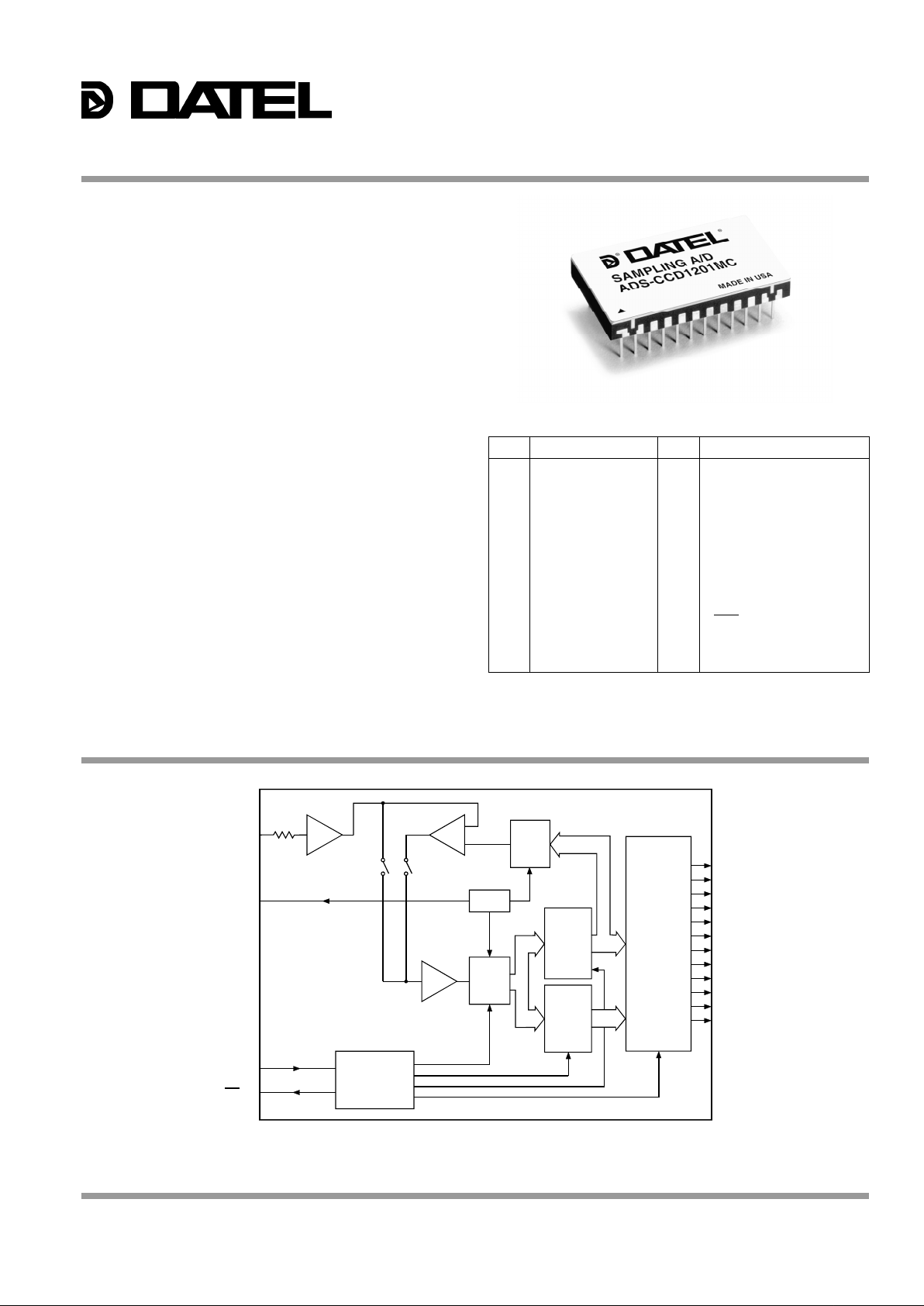
ADS-CCD1201
12-Bit, 1.2MHz, Sampling A/D’s
Optimized for CCD Applications
GENERAL DESCRIPTION
The functionally complete, easy-to-use ADS-CCD1201 is a
12-bit, 1.2MHz Sampling A/D Converter whose performance
and production testing have been optimized for use in
electronic imaging applications, particularly those employing
charge coupled devices (CCD’s) as their photodetectors. The
ADS-CCD1201 delivers the lowest noise (400µVrms) and the
best differential nonlinearity error (±0.35LSB max.) of any
commercially available 12-bit A/D in its speed class. It can
respond to full scale input steps (from empty to full well) with
less than a single count of error, and its input is immune to
overvoltages that may occur due to blooming.
Packaged in an industry-standard, 24-pin, ceramic DDIP, the
ADS-CCD1201 requires ±15V (or ±12V) and +5V supplies and
typically consumes 1.7 (1.4) Watts. The device is 100%
production tested for all critical performance parameters and is
fully specified over both the 0 to +70°C and –55 to +125°C
operating temperature ranges.
For those applications using correlated double sampling, the
ADS-CCD1201 can be supplied without its internal sample-
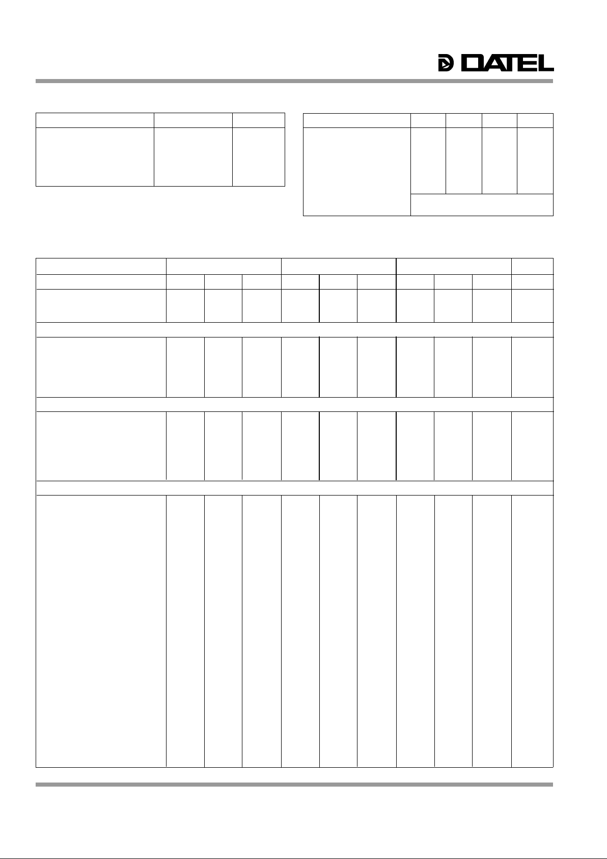
Figure 1. ADS-CCD1201 Functional Block Diagram
INPUT/OUTPUT CONNECTIONS
PIN FUNCTION PIN FUNCTION
1 BIT 12 (LSB) 24 –12V/–15V SUPPLY
2 BIT 11 23 GROUND
3 BIT 10 22 +12V/+15V SUPPLY
4 BIT 9 21 +10V REFERENCE OUT
5 BIT 8 20 ANALOG INPUT
6 BIT7 19 GROUND
7 BIT 6 18 NO CONNECT
8 BIT 5 17 NO CONNECT
9 BIT 4 16 START CONVERT
10 BIT 3 15 EOC
11 BIT 2 14 GROUND
12 BIT 1 (MSB) 13 +5V SUPPLY
• Unipolar input range (0 to +10V)
• 1.2MHz sampling rate
• 4096-to-1 dynamic range (72.2dB)
• Low noise, 400µVrms (1/6 of an LSB)
• Outstanding differential nonlinearity error (±0.35 LSB max.)
• Small, 24-pin ceramic DDIP
• Low power, 1.7 Watts
• Operates from ±12V or ±15V supplies
• Edge-triggered, no pipeline delay
FEATURES
hold amplifier. DATEL will also entertain discussions about
including the CDS circuit internal to the ADS-CCD1201. Please
contact us for more details.
DATEL, Inc. 11 Cabot Boulevard, Mansfield, MA 02048-1151 (U.S.A.) • Tel: (508) 339-3000 Fax: (508)339-6356 • For immediate assistance: (800) 233-2765
FLASH
ADC
REF
DAC
REGISTER
REGISTER
DIGITAL
CORRECTION
LOGIC
12 BIT 1 (MSB)
11 BIT 2
10 BIT 3
9 BIT 4
8 BIT 5
7 BIT 6
6 BIT 7
5 BIT 8
4 BIT 9
3 BIT 10
2 BIT 11
1 BIT 12 (LSB)
TIMING AND
CONTROL LOGIC
ANALOG INPUT 20
START CONVERT 16
EOC 15
13
+5V SUPPLY
17, 18
NO CONNECT
22
+12V/+15V SUPPLY
14, 19, 23
GROUND
24
–12V/–15V SUPPLY
S1
S2
S/H
BUFFER
–
+
+10V REFERENCE
21
Page 2
ADS-CCD1201
®
®
FUNCTIONAL SPECIFICATIONS
(TA = +25°C, ±Vcc = ±15V (or ±12V), +VDD = +5V, 1.2MHz sampling rate, and a minimum 1 minute warmup➀ unless otherwise specified.)
+25°C 0 to +70°C –55 to +125° C
ANALOG INPUT MIN. TYP. MAX. MIN. TYP. MAX. MIN. TYP. MAX. UNITS
Input Voltage Range ➁ — 0 to +10 — — 0 to +10 — — 0 to +10 — Volts
Input Resistance — 1 — — 1 — — 1 — kΩ
Input Capacitance — 7 15 — 7 15 — 7 15 pF
DIGITAL INPUTS
Logic Levels
Logic "1" +2.0 — — +2.0 — — +2.0 — — Volts
Logic "0" — — +0.8 — — +0.8 — — +0.8 Volts
Logic Loading "1" — — +20 — — +20 — — +20 µA
Logic Loading "0" — — –20 — — –20 — — –20 µA
Start Convert Positive Pulse Width ➂ — 100 — — 100 — — 100 — ns
STATIC PERFORMANCE
Resolution — 12 — — 12 — — 12 — Bits
Integral Nonlinearity (fin = 10kHz) — ±0.5 — — ±0.5 — — ±1 — LSB
Differential Nonlinearity (fin = 10kHz) — +0.25 ±0.35 — ±0.25 ±0.35 — ±0.35 ±0.75 LSB
Full Scale Absolute Accuracy — +0.1 ±0.3 — ±0.2 ±0.5 — ±0.3 ±0.5 %FSR
Offset Error (Tech Note 2) — ±0.05 ±0.15 — ±0.1 ±0.15 — ±0.15 ±0.4 %FSR
Gain Error (Tech Note 2) — ±0.1 ±0.3 — ±0.2 ±0.5 — ±0.3 ±0.5 %
No Missing Codes (fin = 10kHz) 12 — — 12 — — 12 — — Bits
DYNAMIC PERFORMANCE
Peak Harmonics (–0.5dB)
dc to 100kHz — –86 –80 — –86 –80 — –82 –76 dB
100kHz to 500kHz — –84 –78 — –84 –78 — –81 –75 dB
Total Harmonic Distortion (–0.5dB)
dc to 100kHz — –84 –79 — –84 –79 — –77 –71 dB
100kHz to 500kHz — –82 –77 — –82 –77 — –76 –70 dB
Signal-to-Noise Ratio
(w/o distortion, –0.5dB)
dc to 100kHz 72 73 — 72 73 — 70 72 — dB
100kHz to 500kHz 71 72 — 71 72 — 70 72 — dB
Signal-to-Noise Ratio ➃
(8 distortion, –0.5dB)
dc to 100kHz 71 73 — 71 73 — 68 71 — dB
100kHz to 500kHz 71 72 — 71 72 — 68 71 — dB
Two-tone Intermodulation Distortion
(fin = 100kHz, 240kHz
fs = 1.2MHz, –0.5dB) — –85 — — –84 — — –83 — dB
Noise — 400 — — 500 — — 700 — µVrms
Input Bandwidth (–3dB)
Small Signal (–20dB input) — 7.5 — — 7.5 — — 7.5 — MHz
Large Signal(–0.5dB input) — 6 — — 6 — — 6 — MHz
Feedthrough Rejection
(fin = 500kHz) — 84 — — 84 — — 84 — dB
Slew Rate — ±60 — — ±60 — — ±60 — V/µs
Aperture Delay Time — ±20 — — ±20 — — ±20 — ns
Aperture Uncertainty — 5 — — 5 — — 5 — ps rms
S/H Acquisition Time
( to ±0.01%FSR, 10V step) 360 400 440 360 400 440 360 400 440 ns
Overvoltage Recovery Time ➄ — 400 833 — 400 833 — 400 833 ns
A/D Conversion Rate 1.2 — — 1.2 — — 1.2 — — MHz
ABSOLUTE MAXIMUM RATINGS
PARAMETERS LIMITS UNITS
+12V/+15V Supply (Pin 22) 0 to +16 Volts
–12V/–15V Supply (Pin 24) 0 to –16 Volts
+5V Supply (Pin 13) 0 to +6 Volts
Digital Input (Pin 16) –0.3 to +V
DD +0.3 Volts
Analog Input (Pin 20) –4 to +17 Volts
Lead Temp. (10 seconds) +300 °C
PHYSICAL/ENVIRONMENTAL
PARAMETERS MIN. TYP. MAX. UNITS
Operating Temp. Range, Case
ADS-CCD1201MC 0 — +70 °C
ADS-CCD1201MM –55 — +125 °C
Thermal Impedance
θ
jc — 5 — °C/Watt
θ
ca — 24 — °C/Watt
Storage Temperature Range –65 – +150 °C
Package Type 24-pin, metal-sealed ceramic DDIP
Weight 0.42 ounces (12 grams)
2.
Page 3
ADS-CCD1201
®
®
Footnotes:
➀ All power supplies must be on before applying a start convert pulse. All
supplies and the clock (START CONVERT) must be present during warmup
periods. The device must be continuously converting during this time. There is
a slight degradation in performance when using ±12V supplies.
➁ Contact DATEL for availability of other input voltage ranges.
➂ A 100ns wide start convert pulse is used for all production testing.
➃ Effective bits is equal to:
➄ This is the time required before the A/D output data is valid after
the analog input is back within the specified range.
+25°C 0 to +70°C –55 to +125°C
ANALOG OUTPUT MIN. TYP. MAX. MIN. TYP. MAX. MIN. TYP. MAX. UNITS
Internal Reference
Voltage +9.95 +10.0 +10.05 +9.95 +10.0 +10.05 +9.95 +10.0 +10.05 Volts
Drift — ±5 — — ±5 — — ±5 — ppm/ºC
External Current — — 1.5 — — 1.5 — — 1.5 mA
DIGITAL OUTPUTS
Logic Levels
Logic "1" +2.4 — — +2.4 — — +2.4 — — Volts
Logic "0" — — +0.4 — — +0.4 — — +0.4 Volts
Logic Loading “1" — — –4 — — –4 — — –4 mA
Logic Loading "0" — — +4 — — +4 — — +4 mA
Delay, Falling Edge of EOC
to Output Data Valid — — 35 — — 35 — — 35 ns
Output Coding Straight Binary
POWER REQUIREMENTS, ±15V
Power Supply Range
+15V Supply +14.5 +15.0 +15.5 +14.5 +15.0 +15.5 +14.5 +15.0 +15.5 Volts
–15V Supply –14.5 –15.0 –15.5 –14.5 –15.0 –15.5 –14.5 –15.0 –15.5 Volts
+5V Supply +4.75 +5.0 +5.25 +4.75 +5.0 +5.25 +4.75 +5.0 +5.25 Volts
Power Supply Current
+15V Supply — +50 +65 — +50 +65 — +50 +65 mA
–15V Supply — –40 –50 — –40 –50 — –40 –50 mA
+5V Supply — +70 +85 — +70 +85 — +70 +85 mA
Power Dissipation — 1.7 1.9 — 1.7 1.9 — 1.7 1.9 Watts
Power Supply Rejection — — ±0.01 — — ±0.01 — — ±0.01 %FSR/%V
POWER REQUIREMENTS, ±12V
Power Supply Range
+12V Supply +11.5 +12.0 +12.5 +11.5 +12.0 +12.5 +11.5 +12.0 +12.5 Volts
–12V Supply –11.5 –12.0 –12.5 –11.5 –12.0 –12.5 –11.5 –12.0 –12.5 Volts
+5V Supply +4.75 +5.0 +5.25 +4.75 +5.0 +5.25 +4.75 +5.0 +5.25 Volts
Power Supply Current
+12V Supply — +50 +65 — +50 +65 — +50 +65 mA
–12V Supply — –40 –48 — –40 –48 — –40 –48 mA
+5V Supply — +70 +80 — +70 +80 — +70 +80 mA
Power Dissipation — 1.4 1.6 — 1.4 1.6 — 1.4 1.6 Watts
Power Supply Rejection — — ±0.01 — — ±0.01 — — ±0.01 %FSR/%V
(SNR + Distortion) – 1.76 + 20 log
Full Scale Amplitude
Actual Input Amplitude
6.02
TECHNICAL NOTES
1. Obtaining fully specified performance from the ADS-CCD1201
requires careful attention to pc-card layout and power supply
decoupling. The device’s analog and digital ground systems are
connected to each other internally. For optimal performance, tie
all ground pins (14, 19, and 23) directly to a large analog
ground plane beneath the package.
Bypass all power supplies, as well as the REFERENCE
OUTPUT (pin 21), to ground with 4.7µF tantalum capacitors in
parallel with 0.1µF ceramic capacitors. Locate the bypass
capacitors as close to the unit as possible. If the user-installed
offset and gain adjusting circuit shown in Figure 2 is used, also
locate it as close to the ADS-CCD1201 as possible.
2. ADS-CCD1201 achieves its specified accuracies without
external calibration. If required, the device’s small initial offset
and gain errors can be reduced to zero using the input circuit of
Figure 2. When using this circuit, or any similar offset and gaincalibration hardware, make adjustments following warmup. To
avoid interaction, always adjust offset before gain.
3. When operating the ADS-CCD1201 from ±12V supplies, do not
drive external circuitry with the REFERENCE OUTPUT (pin 21).
The reference’s accuracy and drift specifications may not be
met, and loading the circuit may cause accuracy errors within
the converter.
4. A passive bandpass filter is used at the input of the A/D for all
production testing.
5. Applying a start pulse while a conversion is in progress (EOC =
logic "1") initiates a new and inaccurate conversion cycle. Data
for the interrupted and subsequent conversions will be invalid.
Input Voltage Zero Adjust Gain Adjust
Range +1/2 LSB +FS – 1 1/2 LSB
0 to +10V +1.2207mV +9.99634V
Table 1. Zero and Gain Adjust
3.
Page 4

ADS-CCD1201
®
®
CALIBRATION PROCEDURE
(Refer to Figures 2 and 3)
Any offset and/or gain calibration procedures should not be
implemented until devices are fully warmed up. To avoid
interaction, offset must be adjusted before gain. The ranges of
adjustment for the circuit of Figure 2 are guaranteed to
compensate for the ADS-CCD1201’s initial accuracy errors and
may not be able to compensate for additional system errors.
Figure 2. ADS-CCD1201 Calibration Circuit
All fixed resistors in Figure 2 should be metal-film types, and
multi-turn potentiometers should have TCR’s of 100ppm/°C or
less to minimize drift with temperature. In many applications,
the CCD will require an offset-adjust (black balance) circuit
near its output and also a gain stage, presumably with adjust
capabilities, to match the output voltage of the CCD to the
input range of the AID. If one is performing a "system I/O
calibration" (from light in to digital out), these circuits can be
used to compensate for the relatively small initial offset and
gain errors of the A/D. This would eliminate the need for the
circuit shown in Figure 2.
Figure 3. Typical ADS-CCD1201 Connection Diagram
A/D converters are calibrated by positioning their digital
outputs exactly on the transition point between two adjacent
digital output codes. This can be accomplished by connecting
LED’s to the digital outputs and adjusting until certain LED’s
"flicker" equally between on and off. Other approaches employ
digital comparators or microcontrollers to detect when the
outputs change from one code to the next.
For the ADS-CCD1201, offset adjusting is normally
accomplished at the point where all output bits are 0’s and the
LSB just changes from a 0 to a 1. This digital output transition
ideally occurs when the applied analog input is +1/2LSB
(+1.2207mV).
Gain adjusting is accomplished when all bits are 1’s and the
LSB just changes from a 1 to a 0. This transition ideally occurs
when the analog input is at +full scale minus 1 1/2 LSB’s
(+9.99634V).
Offset Adjust Procedure
1. Apply a train of pulses to the START CONVERT input (pin
16) so the converter is continuously converting. If using
LED’s on the outputs, a 200kHz conversion rate will reduce
flicker.
2. Apply +1.2207mV to the ANALOG INPUT (pin 20).
3. Adjust the offset potentiometer until the output bits are
0000 0000 00000 and the LSB flickers between 0 and 1.
Gain Adjust Procedure
1. Apply +9.99634V to the ANALOG INPUT (pin 20).
2. Adjust the gain potentiometer until all output bits are 1’s and
the LSB flickers between 1 and 0.
Table 2. ADS-CCD1201 Output Coding
Input Voltage Unipolar Digital Output
(0 to +10V) Scale MSB LSB
+9.9976 +FS – 1LSB 1111 1111 1111
+7.5000 +3/4 FS 1100 0000 0000
+5.0000 +1/2 FS 1000 0000 0000
+2.5000 +1/4 FS 0100 0000 0000
+0.0024 +1LSB 0000 0000 0001
0 0 0000 0000 0000
Coding is straight binary; 1LSB = 2.44mV
All DATEL sampling A/D converters are fully characterized and
specified over operating temperature (case) ranges of 0 to
+70°C and – 55 to +125°C. All room-temperature (T
A = +25°C)
production testing is performed without the use of heat sinks or
forced-air cooling. Thermal impedance figures for each device
are listed in their respective specification tables.
These devices do not normally require heat sinks, however,
standard precautionary design and layout procedures should
be used to ensure devices do not overheat. The ground and
power planes beneath the package, as well as all pcb signal
runs to and from the device, should be as heavy as possible to
help conduct heat away from the package. Electricallyinsulating, thermally-conductive "pads" may be installed
underneath the package. Devices should be soldered to boards
rather than "socketed," and of course, minimal air flow over the
surface can greatly help reduce the package temperature.
In more severe ambient conditions, the package/junction
temperature of a given device can be reduced dramatically
(typically 35%) by using one of DATEL’s HS Series heat sinks.
See Ordering Information for the assigned part number. See
page 1-183 of the DATEL Data Acquisition Components
Catalog for more information on the HS Series. Request DATEL
Application Note AN-8, "Heat Sinks for DIP Data Converters,"or
contact DATEL directly, for additional information.
THERMAL REQUIREMENTS
4.
To Pin 20 of
ADS-CCD1201
–15V
SIGNAL
INPUT
GAIN
ADJUST
1.98k
50
+15V
2k
200k20k
–15V
+15V
ZERO/
OFFSET
ADJUST
Ω
Ω
Ω
Ω
Ω
13
ADS-CCD1201
14
20
15
12
11
10
9
8
7
6
5
4
3
2
1
BIT 1 (MSB)
BIT 2
BIT 3
BIT 4
BIT 5
BIT 6
BIT 7
BIT 8
BIT 9
BIT 10
BIT 11
BIT 12 (LSB)
EOC
ANALOG
INPUT
19, 23
22
24
0.1µF
4.7µF
+5V
0.1µF
4.7µF
0.1µF
4.7µF
+
+
–12V/–15V
+12V/+15V
+
0.1µF
+
4.7µF
21 +10V REF. OUT
0 to +10V
NO CONNECT
17, 18
Page 5

ADS-CCD1201
®
®
TIMING
The ADSCCD-1201 is an edge triggered device. A conversion
is initiated by the rising edge of the start convert pulse and no
additional external timing signals are required. The device does
not employ "pipeline" delays to increase its throughput rate. It
does not require multiple start convert pulses to bring valid
digital data to its output pins.
Figure 5.
ADS-CCD1201 Evaluation Board Schematic
32
30
28
26
24
22
20
33
6
8
10
12
14
16
18
31
27
29
23
25
19
21
3
5
7
9
11
13
15
P2
17
1
2
4
34
5%200K
R3
0.1%
1.98K
R4
–
+
U6
2
3
4
6
7
OP-77
1Y1
1Y2
1Y3
1Y4
2Y1
2Y2
2Y3
2Y4
1G
2G
2A4
2A3
2A2
2A1
1A4
1A3
1A2
1A1
U3
2
4
6
8
11
13
15
17
19
10
20
18
16
14
12
9
7
5
3
1
74LS240
.1%2K
R5
0.1%
10K
R8
P3
P4
74LS86
U4
9
10
8
74LS86
U4
12
13
11
0.1MF
C7
0.1MF
C5
0.1MF
C3
0.1MF
C17
0.1MF
C16
0.1MF
C1
0.1MF
C15
15pF
C2
0.1MF
C10
0.1MF
C12
0.1MF
C13
2.2MF
C6
+
2.2MF
C4
+
2.2MF
C9
+
2.2MF
C8
+
2.2MF
C11
+
2.2MF
C14
+
+5V
+5V
+5V
+5V
+15V
+15V
+15V
+15V
-15V
-15V
-15V
-15V
+5V
P1
12
56
4 3
8 7
10 9
12 11
14 13
16 15
18 17
20 19
22 21
24 23
26
25
20K
R2
50
R1
74LS86
U4
4
5
6
74LS86
U4
1
2
3
7
14
B1
B2
B14
B13
B12
B11
B10
B9
B8
B7
B6
B5
B4
B3
EOC
+5V
DGND
ST. CONV
AGND
INPUT
+10VREF
+15V
AGND
-15V
U1
1
2
3
4
5
6
7
8
9
10
11
12
13
14
15
16
17
18
19
20
21
22
23
24
SG1
–
+
U5
2
3
4
6
7
AD845
0.1%
10K
R7
0.1%
2K
R6
-15V
2.2
MF
C22
+
0.1MF
C23
+15V
2.2MF
C19
+
0.1MF
C20
Y1
1
7
8
14
XTAL
J3
J5
J4
J2
0.1MF
C21
J1
+5V
0.1MF
C18
SG2
SG3
2.2MF
C24
+
1Y1
1Y2
1Y3
1Y4
2Y1
2Y2
2Y3
2Y4
1G
2G
2A4
2A3
2A2
2A1
1A4
1A3
1A2
1A1
U2
2
4
6
8
11
13
15
17
19
10
20
18
16
14
12
9
7
5
3
1
74LS240
B13
B11
B12
B10
B9
B6
B5
B4
B3
B14
B1
B2
B8
B7
SEE NOTE 1
ST.CONV.
ENABLE
MSB
LSB
EOC
COG
ADJ
GAIN
ADJ
OFFSET
CONVERT
START
INPUT
ANALOG
1. FOR ADS-BCCD1201 Y1 IS 1.2MHZ
FOR ADS-BCCD1201 Y1 IS 2MHZ
NOTES:
ADS-CCD1201/1202
Figure 4. ADS-CCD1201 Timing Diagram
5.
START
CONVERT
OUTPUT
DATA
INTERNAL S/H
N
DATA (N-1) VALID
100ns
typ.
Acquisition Time
10ns typ.
DATA N VALID
760ns min.
Note: Scale is approximately 25ns per division.
EOC
90ns typ.
INVALID
DATA
73ns max.
60ns min.,70ns typ., 80ns max.
400ns typ.
433ns typ.
35ns max.
10ns typ.
N+1
100ns
typ.
420ns
Hold
Conversion Time
Page 6

ADS-CCD1201
®
®
SNR (dB)
SNR vs. Input Frequency
1 10 100 1000 10000
Input Frequency (kHz)
90
80
70
60
50
40
30
20
10
0
1 10 100 1000 10000
Input Frequency (kHz)
Peak Harmonic (–dB)
90
80
70
60
50
40
30
20
10
0
Peak Harmonics vs. Input Frequency
SNR+D (dB)
1 10 100 1000 10000
Input Frequency (kHz)
90
80
70
60
50
40
30
20
10
0
SNR+D vs. Input Frequency
Input Frequency (kHz)
THD (–dB)
THD vs. Input Frequency
1 10 100 1000 10000
90
80
70
60
50
40
30
20
10
0
Figure 7. Typical ADS-CCD1201 Dynamic Performance vs. Input Frequency at +25°C
(Vin = –0.5dB, fs = 1.2MHz)
Figure 6. ADS-CCD1201 FFT
(f
in = 480kHz, fs = 1.2MHz, Vin = –0.5dB, 16,384 points)
0
–10
–20
–30
–40
–50
–60
–70
–80
–90
–100
–110
–120
–130
–140
0 60 120 180 240 300 360 420 480 540 600
Frequency (kHz)
Amplitude Relative to Full Scale (dB)
6.
Page 7

ADS-CCD1201
®
®
Figure 9. ADS-CCD1201 Histogram and Differential Nonlinearity
4000
3500
3000
2500
2000
1500
1000
500
0
Digital Output Code
Number of Occurences
Figure 8. ADS-CCD1201 Grounded Input Histogram
7.
This histogram represents the typical
peak-to-peak noise (including
quantization noise) associated with
the ADS-CCD1201. 4,096
conversions were processed with the
input to the ADS-CCD1201 tied to
analog ground.
+0.15
0
–0.19
DNL (LSB's)
0
4096
Number of Occurences
0 4096
Digital Output Code
Digital Output Code
Page 8

0.80 MAX.
(20.32)
0.015
(0.381)
MAX. radius
for any pin
1.31 MAX.
(33.02)
0.100 TYP.
(2.540)
0.100
(2.540)
0.190 MAX.
(4.826)
0.040
(1.016)
0.020 TYP.
(0.508)
0.020
(0.508)
24
13
121
PIN 1
INDEX
0.130 TYP.
(3.302)
Dimension Tolerances
(unless otherwise indicated):
2 place decimal (.XX) ±0.010 (±0.254)
3 place decimal (.XXX) ±0.005 (±0.127)
Lead Material: Kovar alloy
Lead Finish: 50 microinches (minimum) gold plating
over 100 microinches (nominal) nickel plating
0.060 TYP.
(1.524)
0.010 TYP.
(0.254)
MECHANICAL DIMENSIONS INCHES (mm)
24-PIN DDIP
DATEL (UK) LTD. Tadley, England Tel: (01256)-880444
DATEL S.A.R.L. Montigny Le Bretonneux, France Tel: 1-34-60-01-01
DATEL GmbH Munchen, Germany Tel: 89-544334-0
DATEL KK Tokyo, Japan Tel: 3-3779-1031, Osaka Tel: 6-354-2025
DATEL, Inc. 11 Cabot Boulevard, Mansfield, MA 02048-1151
Tel: (508) 339-3000 / Fax: (508) 339-6356
For immediate assistance: (800) 233-2765
DATEL makes no representation that the use of its products in the circuits described herein, or the use of other technical information contained herein, will not infringe upon existing or future patent rights. The descriptions contained
herein do not imply the granting of licenses to make, use, or sell equipment constructed in accordance therewith. Specifications are subject to change without notice. The DATEL logo is a registered DATEL, Inc. trademark.
ADS-CCD1201
®
®
0.200 MAX.
(5.080)
0.235 MAX.
(5.969)
0.600 ±0.010
(15.240)
0.80 MAX.
(20.32)
0.100 TYP.
(2.540)
0.100
(2.540)
0.018 ±0.002
(0.457)
0.100
(2.540)
0.040
(1.016)
1.31 MAX.
(33.27)
1 12
13
24
1.100
(27.940)
0.190 MAX.
(4.826)
0.010
(0.254)
+0.002
–0.001
SEATING
PLANE
0.025
(0.635)
Dimension Tolerances
(unless otherwise indicated):
2 place decimal (.XX) ±0.010 (±0.254)
3 place decimal (.XXX) ±0.005 (±0.127)
Lead Material:
Kovar alloy
Lead Finish:
50 microinches (minimum)
gold plating over 100 microinches
(nominal) nickel plating
OPERATING
MODEL NUMBER TEMP. RANGE ANALOG INPUT
ADS-CCD1201MC 0 to +70°C Unipolar (0 to +10V)
ADS-CCD1201MM –55 to +125°C Unipolar (0 to +10V)
Contact DATEL for availability of surface-mount packaging or
high-reliability screening.
Accessories
ADS-BCCD1201 Evaluation Board (without ADS-CCD1201)
HS-24 Heat Sink for ADS-CCD1201 models
Receptacles for pc board mounting can be ordered through
Amp Inc., part number 3-331272-8 (component lead socket),
24 required.
ORDERING INFORMATION
24-PIN SURFACE MOUNT
®
®
INNOV A TION and EX CELLENCE
ISO 9001
ISO 9001
REGISTERED
DS-0274C 10/96
 Loading...