

Page 1
® ®
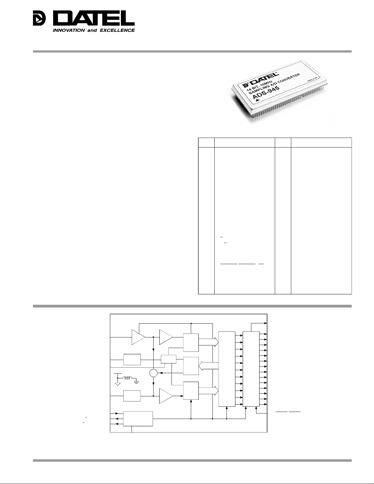
3-STATE OUTPUT REGISTER
DIGITAL CORRECTION LOGIC
SUPPLY
SUPPLY
SUPPLY
GROUND
CONNECT
SUPPLY
FEATURES
• 14-bit resolution
• 10MHz minimum throughput
• Functionally complete
• No missing codes
• Low power, 4.2W
• Excellent dynamic performance
• Internally clamped input
• Edge triggered
• TTL compatible
• 2" x 4" module
• Very low profile
GENERAL DESCRIPTION
The low-cost ADS-945 is a high-performance, 14-bit, 10MHz
sampling A/D converter. This device accurately samples
full-scale input signals up to Nyquist frequencies with no
missing codes. The dynamic performance of the ADS-945
has been optimized to achieve a THD of –82dB and a
SNR of 79dB.
Packaged in a 2" x 4" module, the functionally complete
ADS-945 contains a fast-settling sample/hold amplifier, a
subranging (two-pass) A/D converter, a precise voltage
reference, timing/control logic, three-state outputs, and
error-correction circuitry. Digital inputs and outputs are TTL
compatible (except for pins 29 and 30 which are ECL).
Requiring ±15V, +5V and –5.2V supplies, the ADS-945
typically dissipates 4.2W. The unit is offered with a bipolar
input range of ±1.25V. Models are available for use in either
commercial (0 to +70°C) or military (–55 to +125°C) operating
temperature ranges. Typical applications include radar signal
analysis, medical/graphic imaging, and FFT spectrum
analysis.
ADS-945
14-Bit, 10MHz
Sampling A/D Converters
INPUT/OUTPUT CONNECTIONS
PIN FUNCTION PIN FUNCTION
1 ANALOG GROUND 70-76 ANALOG GROUND
4 ANALOG INPUT 69 +5V ANALOG SUPPLY
5-6 ANALOG GROUND 64-68 ANALOG GROUND
7 +10V REFERENCE OUT 63 –5.2V ANALOG SUPPLY
8 ANALOG GROUND 62 ANALOG GROUND
9 GAIN ADJUST 61 NO CONNECT
10-11 DO NOT CONNECT 58-60 DIGITAL GROUND
12 –15V SUPPLY 57 –5.2V DIGITAL SUPPLY
13 ANALOG GROUND 56 DO NOT CONNECT
14 +15V SUPPLY 55 +5V DIGITAL SUPPLY
15-17 ANALOG GROUND 54 DIGITAL GROUND
18 OFFSET ADJUST 53 BIT 1 (MSB)
19-25 ANALOG GROUND 52 BIT 2
26 MISSING PIN 51 BIT 3
27 DIGITAL GROUND 50 BIT 4
28 DIGITAL GROUND 49 BIT 5
29 T/H STATUS 48 BIT 6
30 T/H STATUS 47 BIT 7
31 DIGITAL GROUND 46 BIT 8
32 START CONVERT 45 BIT 9
33 OVERFLOW 44 BIT 10
34 OUTPUT ENABLE (OE) 43 BIT 11
35 DIGITAL GROUND 42 BIT 12
36 O.S. 3 * 41 BIT 13
37 DIGITAL GROUND 40 BIT 14 (LSB)
38 DIGITAL GROUND 39 DIGITAL GROUND
* Refer to Timing Diagram notes
33 OVERFLOW
53
BIT 1 (MSB)
52
BIT 2
51
BIT 3
50
BIT 4
49
BIT 5
48
BIT 6
47
BIT 7
46
BIT 8
45
BIT 9
44
BIT 10
43
BIT 11
42
BIT 12
41
BIT 13
40
BIT 14 (LSB)
34 OUTPUT ENABLE
26 MISSING PIN
10,11,56 DO NOT CONNECT
57
ANALOG INPUT 4
GAIN ADJUST 9
+10 REF. OUT 7
1,2,3,5,6,8,13,15,17,
19-25,62,64-68,70-76
ANALOG GROUND
OFFSET ADJUST 18
START CONVERT 32
T/H STATUS 29
T/H STATUS 30
CASE
AGND
12
–15V
+1
T/H
GAIN
CIRCUIT
DGND
OFFSET
CIRCUIT
TIMING AND
CONTROL LOGIC
36
+15V
O.S. 3
Σ
AMP
14
27,28,31,35,37-39,54,58-60
BUFFER
REF
DIGITAL
FLASH
ADC
1
DAC
FLASH
ADC
2
61
NO
55
+5V DIGITAL
–5.2V DIGITAL
Figure 1. ADS-945 Functional Block Diagram
DATEL, Inc., 11 Cabot Boulevard, Mansfield, MA 02048-1151 (U.S.A.) • Tel: (508) 339-3000 Fax: (508) 339-6356 • For immediate assistance: (800) 233-2765
Page 2
ADS-945
® ®
ABSOLUTE MAXIMUM RATINGS
PARAMETERS LIMITS UNITS
+15V Supply (Pins 14) 0 to +17 Volts
–15V Supply (Pin 12) 0 to –17 Volts
+5V Supply (Pins 55, 69) 0 to +6 Volts
–5V Supply (Pin 57, 63) 0 to –6 Volts
Digital Input (Pin 32, 34) –0.3 to +V
Analog Input (Pin 4) –5 to +5 Volts
Lead Temperature (10 seconds) +300 °C
DD +0.3 Volts
PHYSICAL/ENVIRONMENTAL
PARAMETERS MIN. TYP. MAX. UNITS
Operating Temp. Range, Case
ADS-945 0 — +70 °C
ADS-945EX –55 — +125 °C
Thermal Impedance
θjc — 10 — °C/Watt
θca — 8 — °C/Watt
Storage Temperature Range –65 — +150 °C
Package Type 2" x 4" module
Weight 2.1 oz. (60 grams)
FUNCTIONAL SPECIFICATIONS
(TA = +25°C, ±VCC = ±15V, +VDD = +5V, VDD = –5.2V, 10MHz sampling rate, and a minimum 10 minute warmup ➀ unless otherwise specified.)
+25°C 0 to +70°C –55 to +125°C
ANALOG INPUT MIN. TYP. MAX. MIN. TYP. MAX. MIN. TYP. MAX. UNITS
Input Voltage Range ➁ — ±1.25 — — ±1.25 — — ±1.25 — Volts
Input Resistance 300 500 — 300 550 — 300 500 — kΩ
Input Capacitance — 10 15 — 10 15 — 10 15 pF
Input Bias Current — ±3 — — ±3 — — ±3 — µA
DIGITAL INPUT
Logic Levels
Logic "1" +2.0 — — +2.0 — — +2.0 — — Volts
Logic "0" — — +0.8 — — +0.8 — — +0.8 Volts
Logic Loading "1" — — +20 — — +20 — — +20 µA
Logic Loading "0" — — –20 — — –20 — — –20 µA
Start Convert Positive Pulse Width ➂ 10 50 — 10 50 — 10 50 — ns
STATIC PERFORMANCE
Resolution — 14 — — 14 — — 14 — Bits
Integral Nonlinearity (f
Differential Nonlinearity (f
in = 10kHz) — ±0.5 — — ±0.75 — — ±0.75 — LSB
in = 10kHz) — ±0.5 ±0.75 — ±0.5 ±0.75 –0.95 ±0.75 +1.5 LSB
Full Scale Absolute Accuracy — ±0.2 ±0.4 — ±0.3 ±0.5 — ±0.3 ±0.7 %FSR
Bipolar Offset Error (Tech Note 2) — ±0.15 ±0.25 — ±0.25 ±0.5 — ±0.3 ±0.7 %FSR
Gain Error (Tech Note 2) — ±0.1 ±0.2 — ±0.2 ±0.4 — ±0.3 ±0.7 %
No Missing Codes (f
in = 10kHz) 14 — — 14 — — 14 — — Bits
DYNAMIC PERFORMANCE
Peak Harmonics (–0.5dB)
dc to 1mHz — –86 –78 — –86 –78 — –80 –72 dB
1MHz to 2.5MHz — –82 –75 — –82 –75 — –79 –70 dB
2.5MHz to 5MHz — –79 –74 — –79 –74 — –78 –70 dB
Total Harmonic Distortion (–0.5dB)
dc to 1MHz — –82 –76 — –82 –76 — –78 –70 dB
1MHz to 2.5MHz — –80 –74 — –80 –74 — –76 –68 dB
2.5MHz to 5MHz — –78 –73 — –78 –73 — –76 –68 dB
Signal-to-Noise Ratio
(w/o distortion, –0.5dB)
dc to 1MHz 76 79 — 76 79 — 70 78 — dB
100kHz to 2.5MHz 76 78 — 76 78 — 70 77 — dB
2.5MHz to 5MHz 75 77 — 75 77 — 70 75 — dB
Signal-to-Noise Ratio ➃
(& distortion, –0.5dB)
dc to 100kHz 73 77 — 73 77 — 67 74 — dB
1MHz to 2.5MHz 72 76 — 72 76 — 67 74 — dB
2.5MHz to 5MHz 71 74 — 71 74 — 66 72 — dB
Noise — 110 — — 110 — — 110 — µVrms
Two-tone Intermodulation
Distortion (f
2.45MHz, f
in = 1.975MHz,
s = 10MHz, –0.5dB) — –84 — — –84 — — –84 — dB
Input Bandwidth (–3dB)
Small Signal (–20dB input) — 100 — — 100 — — 100 — MHz
Large Signal (–0.dB input) — 50 — — 50 — — 50 — MHz
Feedthrough Rejection (f
in = 4.85MHz) — 90 — — 90 — — 90 — dB
Slew Rate — ±850 — — ±850 — — ±850 — V/µs
Aperture Delay Time — +8 — — +8 — — +8 — ns
Aperture Uncertainty — 2 — — 2 — — 2 — ps rms
2
Page 3
® ®
ADS-945
+25°C 0 to +70°C –55 to +125°C
DYNAMIC PERFORMANCE cont. MIN. TYP. MAX. MIN. TYP. MAX. MIN. TYP. MAX. UNITS
S/H Acquisition Time
( to ±0.003%FSR, 2.5V step) — 40 — — 40 — — 40 — ns
Overvoltage Recovery Time ➄ — 30 100 — 30 100 — 30 100 ns
A/D Conversion Rate 10 — — 10 — — 10 — — MHz
ANALOG OUTPUT
Reference Output +9.99 +10 +10.01 +9.99 +10 +10.01 +9.99 +10 +10.01 Volts
Reference Temperature Drift — ±40 — — ±40 — — ±40 — ppm/°C
Reference Load Curent — — 2.0 — — 2.0 — — 2.0 mA
DIGITAL OUTPUTS
Logic Levels
Logic "1" +2.7 — — +2.7 — — +2.7 — — Volts
Logic "0" — — +0.5 — — +0.5 — — +0.5 Volts
Logic Loading "1" — — –0.4 — — –0.4 — — –0.4 mA
Logic Loading "0" — — +8 — — +8 — — +8 mA
Delay, Falling Edge of T/H
to Output Data Valid — 55 — — 55 — — 55 — ns
Delay, Edge of ENABLE
to Output Data Valid/Invalid — — 18 — — 18 — — 18 ns
Output Coding
POWER REQUIREMENTS
Complementary Offset Binary
Power Supply Ranges
+15V Supply +14.25 +15.0 +15.75 +14.25 +15.0 +15.75 +14.25 +15.0 +15.75 Volts
–15V Supply –14.25 –15.0 –15.75 –14.25 –15.0 –15.75 –14.25 –15.0 –15.75 Volts
+5V Supply +4.75 +5.0 +5.25 +4.75 +5.0 +5.25 +4.75 +5.0 +5.25 Volts
–5.2V Supply –4.95 –5.2 –5.45 –4.95 –5.2 –5.45 –4.95 –5.2 –5.45 Volts
Power Supply Currents ➅
+15V Supply — +35 +45 — +35 +45 — +35 +45 mA
–15V Supply — –55 –65 — –55 –65 — –55 –65 mA
+5V Supply — +140 +160 — +140 +160 — +140 +160 mA
–5.2V Supply — –430 –460 — –430 –460 — –430 –460 mA
Power Dissipation — 4.2 4.5 — 4.2 4.5 — 4.2 4.5 Watts
Power Supply Rejection — — ±0.04 — — ±0.04 — — ±0.04 %FSR/%V
Footnotes:
➀ All power supplies should be on before applying a start convert pulse. All
supplies and the clock (start convert pulses) must be present during warmup
periods. The device must be continuously converting during this time.
➁ The input to the ADS-945 is internally clamped at ±2.3V.
➂ An 50ns wide start convert pulse is used for all production testing. For
applications requiring less than a 10MHz sampling rate, a wider start convert
can be used.
TECHNICAL NOTES
1. Obtaining fully specified performance from the ADS-945
requires careful attention to pc-card layout and power
supply decoupling. The device's analog and digital ground
systems are connected to each other internally. For optimal
performance, tie all ground pins directly to a large analog
ground plane beneath the package.
Bypass all power supplies to ground with 10µF tantalum
capacitors in parallel with 0.1µF ceramic capacitors. The
bypass capacitors should be located as close to the
unit as possible.
2. The ADS-945 achieves its specified accuracies without the
need for external calibration. If required, the device's small
initial offset and gain errors can be reduced to zero using
➃ Effective bits is equal to:
(SNR + Distortion) – 1.76 + 20 log
➄ This is the time required before the A/D output is valid after the analog input is
back within its range.
➅ Typical +5V and –5.2V current drain breakdowns are as follows:
Analog = +100mA –5.2VAnalog= –210mA
+5V
Digital = +40mA –5.2VDigital = –220mA
+5V
+5VTotal = +140mA –5.2VTotal = –430mA
Full Scale Amplitude
Actual Input Amplitude
6.02
the adjustment circuitry shown in Figure 2. The typical
adjustment range is ±0.2%FSR for this circuitry.
When using this circuitry, or any similar offset and gaincalibration hardware, make adjustments following warmup.
To avoid interaction, always adjust offset before gain.
3. To enable the three-state outputs, apply a logic "0" (low) to
OUTPUT ENABLE (pin 34). To disable, apply a logic "1"
(high) to pin 34.
4. A passive bandpass filter (Allen Avionics F4202 Series) is
used at the input of the A/D for all production testing.
5. The ADS-945's digital outputs should not be directly
connected to a noisy data bus. Drive the bus with 573 or
574 type latches and use "low-noise" logic, such as the
74LS series.
3
Page 4

ADS-945
+ +
+ +
+ +
–15V
® ®
CALIBRATION PROCEDURE
(Refer to Figure 2 and Table 1)
Note: Connect pin 18 to ANALOG GROUND (pin 19) for
operation without zero/offset adjustment. Connect pin 9 to
ANALOG GROUND (pin 8) for operation without gain
adjustment.
Any offset and/or gain calibration procedures should not be
implemented until devices are fully warmed up. To avoid
interaction, offset must be adjusted before gain. The ranges of
adjustment for the circuit in Figure 2 are guaranteed to
compensate for the ADS-945's initial accuracy errors and may
not be able to compensate for additional system errors.
A/D converters are calibrated by positioning their digital
outputs exactly on the transition point between two adjacent
digital output codes. This can be accomplished by connecting
LED's to the digital outputs and adjusting until certain LED's
"flicker" equally between on and off. Other approaches
employ digital comparators or microcontrollers to detect when
the outputs change from one code to the next.
For the ADS-945, offset adjusting is normally accomplished at
the point where the MSB is a 1 and all other output bits are 0's
and the LSB just changes from a 0 to a 1. This digital output
transition ideally occurs when the applied analog input is
+½ LSB (+76.3
Gain adjusting is accomplished when all bits are 0's and the
LSB just changes from a 0 to a 1. This transition ideally
occurs when the analog input is at +full scale minus 1 ½ LSB's
(+1.249771V) .
Note: Due to inherent system noise, the averaging of
several conversions may be needed to accurately
adjust both offset and gain to 1LSB of accuracy.
µV).
Zero/Offset Adjust Procedure
1. Apply a train of pulses to the START CONVERT input
(pin 32) so the converter is continuously converting.
2. Apply +76.3
µV to the ANALOG INPUT (pin 4).
3. Adjust the offset potentiometer until the output bits are
10 0000 0000 0000 and the LSB flickers between 0 and 1.
Gain Adjust Procedure
1. Apply +1.249771V to the ANALOG INPUT (pin 4).
2. Adjust the gain potentiometer until all output bits are 0's
and the LSB flickers between 0 and 1.
3. To confirm proper operation of the device, vary the applied
input voltage to obtain the output coding listed in Table 1.
Note: A single +5V supply can be used for both the +5V
ANALOG and the +5V DIGITAL. If separate supplies are
used, the difference between the two can not exceed
100mV. This also applies to the –5.2V supply requirements.
Datel recommends using ferrite beads to separate the analog
and digital supplies (FAIR-RITE # 2643000301.)
Table 1. Output Coding
OUTPUT CODING INPUT RANGE BIPOLAR
MSB LSB ±1.25V SCALE
00 0000 0000 0000 +1.249847 +FS –1 LSB
00 0111 1111 1111 +0.937500 +3/4 FS
00 1111 1111 1111 +0.625000 +1/2FS
01 1111 1111 1111 0.000000 0
10 1111 1111 1111 –0.625000 –1/2FS
11 0111 1111 1111 –0.937500 –3/4FS
11 1111 1111 1110 –1.249847 –FS +1 LSB
11 1111 1111 1111 –1.250000 –FS
COMP. OFF. BINARY
BIT 1 (MSB)
53
BIT 2
52
BIT 3
51
BIT 4
50
BIT 5
49
BIT 6
48
BIT 7
47
46
BIT 8
45
BIT 9
44
BIT 10
43
BIT 11
BIT 12
42
BIT 13
41
BIT 14 (LSB)
40
OUTPUT ENABLE
34
OVERFLOW
33
T/H STATUS
30
T/H STATUS
29
ANALOG INPUT
4
32START CONVERT
7
+15V
9
0.1µF
20k
Ω
+5V
10µF
0.1µF
10µF
10µF
10µF
10µF
10µF
+15V
20kΩ
–15V
0.1µF
0.1µF
0.1µF
0.1µF
0.1µF
–5.2V
+5V
–5.2V
+15V
–15V
55
54
58-60
57
69
64-68
63
12
13
15-17
13
18
DIGITAL
SUPPLY
DIGITAL
GROUND
DIGITAL
SUPPLY
ANALOG
SUPPLY
ANALOG
GROUND
ANALOG
SUPPLY
ANALOG
GROUND
OFFSET
ADJUST
ADS-945
+10 REF. OUT
GAIN
ADJUST
Figure 2. ADS-945 Connection Diagram
4
Page 5

®®
ADS-945
AGND
BIT 8
BIT 7
BIT 6
BIT 5
129
147
Q5Q4Q3Q2Q1
ALS573
8D7D6D5D4D
813
615
-5.2VA
C20
L11
L10
SG3
-5.2VD
OFFSET
P2
CONNECTOR
DATA OUTPUT
34 33
1
DATA
Q8Q7Q6
OC
10
GND
CP
11
+5VA
C21
SG1
+5VD
DNC
+5VD
-5.2VD
32 31
30 29
28 27
26 25
24 23
22 21
20 19
C28
LATCHES
BIT 1
BIT 2
(MSB)
BIT 3
BIT 4
20
219
BIT 6
BIT 5
T/H
Q1
+5V
1D
BIT 7
T/H
DGND
SG4
AGND
SG2
MSB BIT 1
DGND
L7
C27
C29
D
+5V
+5VA
76757473727170696867666564636261605958575655545352515049484746454443424140
U1
ADS945
IN
1
+
C18
+5VA
GAIN
VREF
9
8765432
10
BIT 3
BIT 2
183
20
+5V
3D
2D
1D
417
219
C19
-5.2VA
+15V
-15V
BIT 4
165
U6
-5.2VA
18 17
16 15
14 13
BIT 9
BIT 10
BIT 11
165
183
U7
3D
2D
417
BIT 9
BIT 8
BIT 10
CLOCK
O.F.
9
87
12 11
10
BIT 12
BIT 13
LSB BIT 14
147
ALS573
813
615
BIT 13
BIT 12
BIT 11
ENABLE
ENABLE
65
43
21
EOC
CLOCK
OVERFLOW
1
129
Q8Q7Q6Q5Q4Q3Q2
OC
10
GND
CP
8D7D6D5D4D
11
3938
(LSB) BIT 14
OS3
373635343332313029282726252423222120191817161514131211
10K
R12
C16
+15V
C15
-15V
CW
C14
3
2
R1
20K
1
GAIN
+15V
51.1
R5
2
3
1
JPR3
NC
P3
-5.2VA
+15V+5VA+5V
-5.2VA-5.2V -15V
0.1" GRID
D
HOLE PATTERN
D
C17
CW
-15V
3
OFFSET
R2
20K
2
D
1
+15V
-15V
C1
+
D1
P1
POWER SUPPLY
+5V
C22
+5VA/350MA
C2
+
D2
L2
L3
L1
-5.2V
+5VD
-5.2VD
CONNECTOR
26 25
24 23
22 21
20 19
18 17
16 15
14 13
+V
-V
3
2
1
U4
LT1016
6
5
7
8
D
+5V
-15V/80MA
C3
+
D3
L5
L4
-15V
+15V
12 11
10 9
87
65
4
C23
L6
43
C9
10PF
(OPT)
D
-5.2V
INT
1
X1
8
10MHZ
14
1,7
C26
+15V/50MA
C4
+
D4
+5VA
21
EXT
2
1
2
EXT
3
JPR2
CLOCK
3
JPR1
OUTPUT ENABLE
INT
ALL RESISTORS ARE IN OHMS RN55C.
UNLESS OTHERWISE SPECIFIED.
1.
NOTES:
10UFD 25V.
ALL POLORIZED CAPACITORS ARE
R3
51.1
P4
EXT. CLOCK
0.1UFD 50V.
N.C. POSITION.
2UHY.
1N4001.
ALL NON POLORIZED CAPACITORS ARE
C9 NOT TO BE INSTALLED.
INSTALL IN SOCKET (ITEM 34).
FOR X1 USE MONITOR OSCILLATOR TYPE 970T,
ALL CHOKES ARE
ALL DIODES ARE
ALL SWITCHES ARE SHOWN IN THE
2.
3.
4. REMOVE X1 IF USING EXTERNAL CLOC K .
Figure 3. ADS-945 Evaluation Board Schematic (DATEL Dwg. #A-23442)
5
Page 6

ADS-945
Digital Output Code
CONVERT
Note: Scale is approximately 10ns per division.
DATA
Amplitude Relative to Full Scale (dB)
(fs = 10MHz, fin = 4.85MHz, Vin = –0.5dB, 16,384-point FFT)
kHz MHz MHz MHz MHz MHz MHz MHz MHz MHz
® ®
N
START
50ns typ.
10ns typ.
T/H
60ns typ.
T/H
OUTPUT
DATA
Hold
DATA N-1 VALID
Figure 4. ADS-945 Timing Diagram
Timing Notes:
1. The ADS-945 is an edge-triggered device requiring no
additional external timing signals. The rising edge of the
start convert pulse initiates a conversion.
2. A start convert pulse of 50ns is recommended when
sampling at 10MHz.
55ns typ.
INVALID
N+1
N+2
Acquisition Time
Hold
40ns typ.
Hold
10ns typ.
DATA N VALID
90ns typ.
DATA N+1 VALID
3. The falling edge of the subsequent start convert pulse
(N+1) or the rising edge of the N+2 pulse can be used to
latch data from conversion N (1 pipeline delay).
4. For a sampling rate of 10MHz, do not connect pin 36.
5. For sampling rates between 7.75 and 8.25MHz, place a
22pF capacitor to digital ground on pin 36.
0
–10
–20
–30
–40
–50
–60
–70
–80
–90
–100
–110
–120
–130
–140
–150
0 500 1 1.5 2 2.5 3 3.5 4 4.5 5
Frequency
Figure 5. ADS-945 FFT Analysis
9000
8000
7000
6000
5000
4000
3000
2000
1000
0
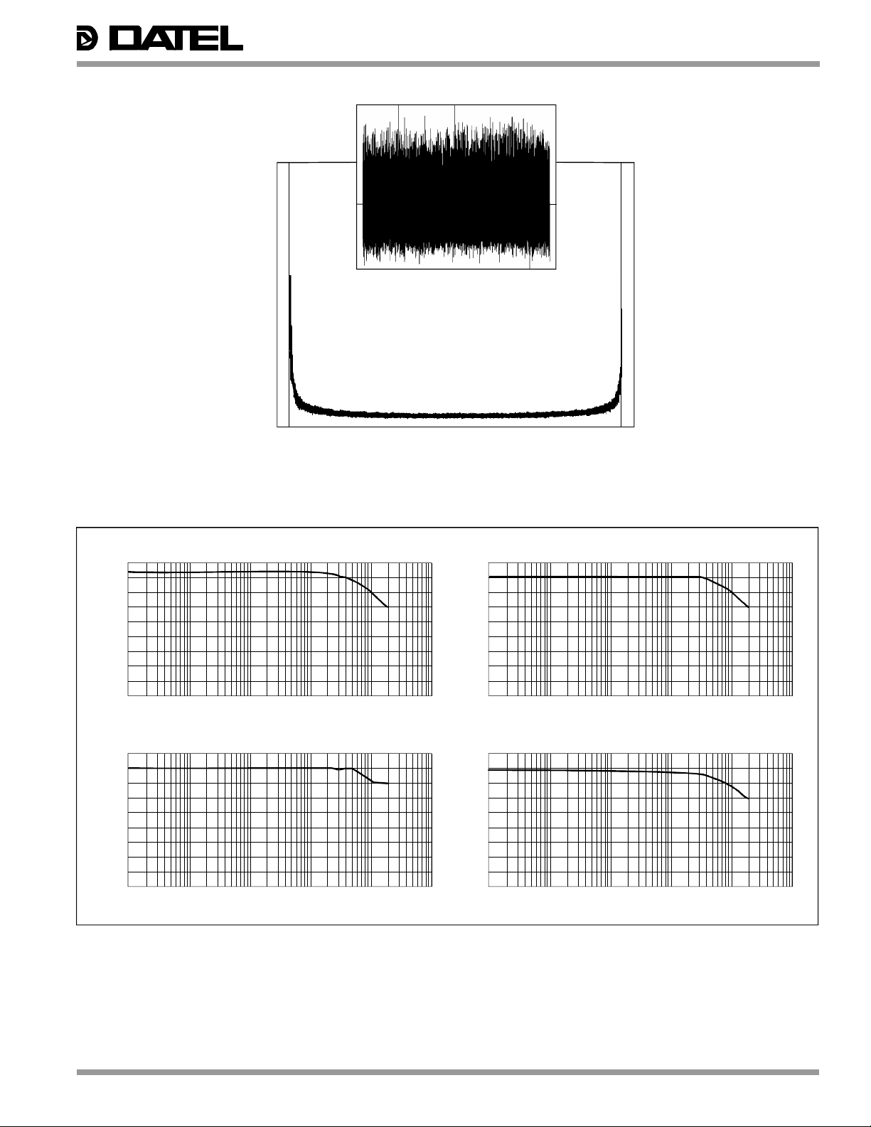
Figure 6. ADS-945 Grounded Input Histogram
This histogram represents the typical peak-to-peak noise
(including quantization noise) associated with the ADS-945.
16,384 conversions were processed with the input to the
ADS-945 tied to analog ground.
6
Page 7
® ®
Peak Harmonic (–dB)
SNR (dB)
SNR+D (dB)
THD (–dB)
1 10 100 1000 10000 100000
Frequency (kHz)
Peak Harmonic (–dB)
THD (–dB)
1 10 100 1000 10000 100000
Frequency (kHz)
Number of Occurences
Digital Output Code
16,384
DNL (LSB's)
ADS-945
+0.39
0
–0.29
0
Digital Output Code
0
16,384
Figure 7. ADS-945 Histogram and Differential Nonlinearity
90
80
70
60
50
40
30
20
10
0
1 10 100 1000 10000 100000
90
80
70
60
50
40
30
20
10
0
1 10 100 1000 10000 100000
PH vs. Input Frequency
Frequency (kHz)
90
80
70
60
50
40
30
20
10
0
90
80
70
60
50
40
30
20
10
0
THD vs. Input Frequency
Frequency (kHz)
SNR+D vs. Input FrequencySNR vs. Input Frequency
Figure 8. ADS-945 Dynamic Performance vs. Input Frequency at +25°C
7
Page 8

ADS-945
ISO 9001
REGISTERED
(FR-4) base
39
1.80
(45.72)
0.100 (2.54) TYP.
MECHANICAL DIMENSIONS INCHES (mm)
0.29 MAX.
(7.37)
0.15 MIN.
(3.81)
0.06 (1.52)
2.06 MAX.
(52.32)
® ®
76
3.700
(93.98)
1
Missing pin 26
is for keying
purposes
0.25 Square
38
Insulated surface with
internal ground plane
(6.35) TYP.
Epoxy glass
4.02
(102.11)
MAX.
Metal case
2.02 MAX.
(51.31)
4.06
(103.12)
MAX.
MODEL NUMBER OPERATING TEMP. RANGE
ADS-945 0 to +70°C
ADS-945EX –55 to +125°C
DATEL, Inc. 11 Cabot Boulevard, Mansfield, MA 02048-1151
Tel: (508) 339-3000 (800) 233-2765 Fax: (508) 339-6356
Internet: www.datel.com E-mail:sales@datel.com
Data Sheet Fax Back: (508) 261-2857
DATEL makes no representation that the use of its products in the circuits described herein, or the use of other technical information contained herein, will not infringe upon existing or future patent rights. The descriptions contained herein
do not imply the granting of licenses to make, use, or sell equipment constructed in accordance therewith. Specifications are subject to change without notice. The DATEL logo is a registered DATEL, Inc. trademark.
ORDERING INFORMATION
ACCESSORIES
ADS-945 Evaluation Board (without ADS-945)
ISO 9001
DS-0237E 01/96
DATEL (UK) LTD. Tadley, England Tel: (01256)-880444
DATEL S.A.R.L. Montigny Le Bretonneux, France Tel: 1-34-60-01-01
DATEL GmbH München, Germany Tel: 89-544334-0
DATEL KK Tokyo, Japan Tel: 3-3779-1031, Osaka Tel: 6-354-2025
 Loading...