

Page 1
® ®
REGISTERREGISTER
DIGITAL CORRECTION LOGIC
GROUND
GROUND
SUPPLY
3-STATE OUTPUT REGISTER
SUPPLY
GROUND
SELECT
SUPPLY
FEATURES
• 14-bit resolution
• 2MHz minimum throughput
• Functionally complete
• Internal reference and sample/hold
• -85dB total harmonic distortion
• 78dB signal-to-noise ratio
• Full Nyquist-rate sampling
• Small 32-pin DIP
• Low-power, 2.9 Watts
ADS-942
14-Bit, 2MHz
Sampling A/D Converters
GENERAL DESCRIPTION
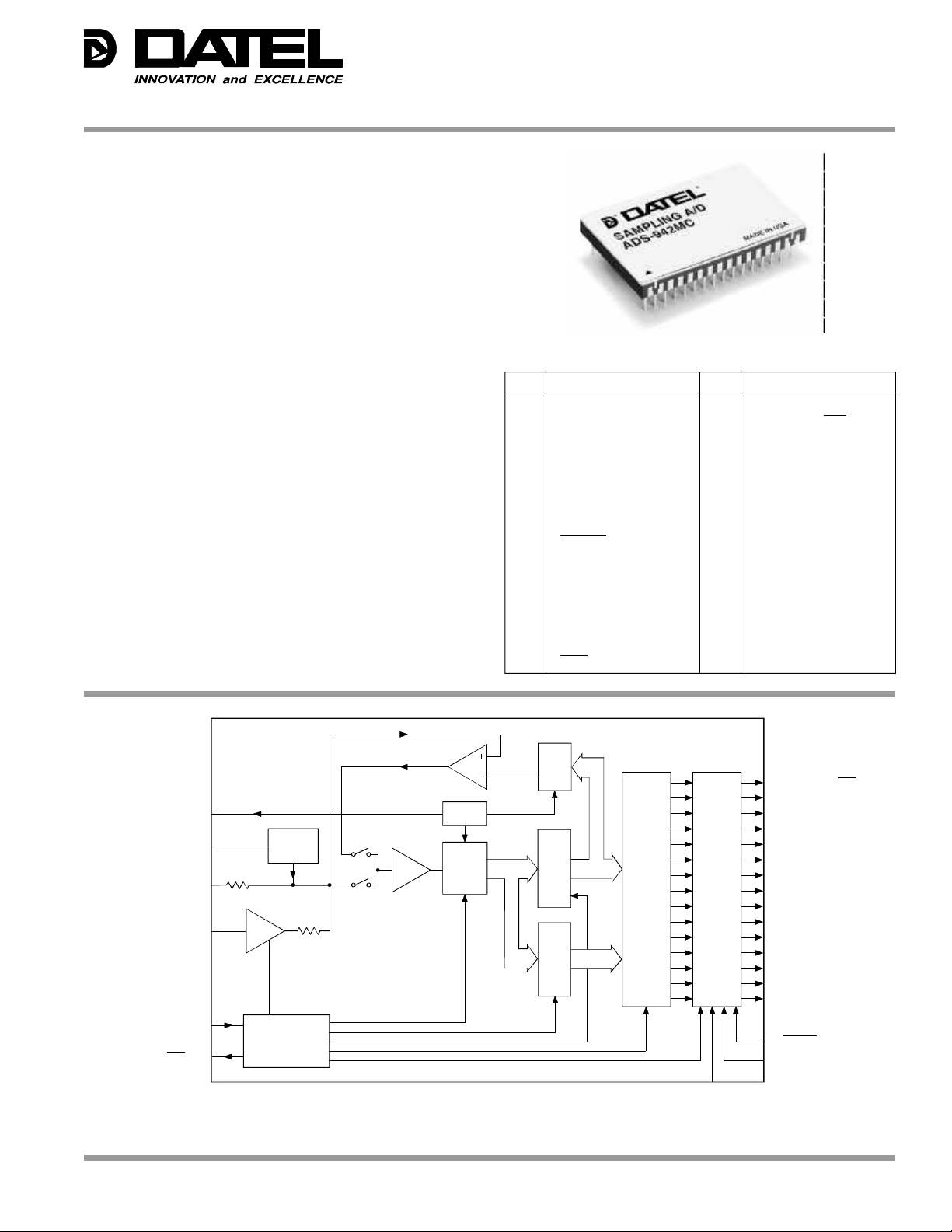
DATEL's ADS-942 is a functionally complete, 14-bit, 2MHz,
sampling A/D converter. Its standard, 32-pin, triple-wide
ceramic DIP contains a fast-settling sample/hold amplifier, a
14-bit subranging (two-pass) A/D converter, a precision
reference, three-state output register and all the timing and
control logic necessary to operate from a single start
convert pulse.
The ADS-942 is optimized for wideband frequency-domain
applications and is fully FFT tested. The ADS-942 requires
±15V and +5V supplies and typically consumes 2.9 Watts.
+10V REF. OUT 1
OFFSET ADJUST 5
BIPOLAR 2
ANALOG INPUT 3
START CONVERT 32
EOC 16
OFFSET
CIRCUIT
S/H
TIMING AND
CONTROL LOGIC
S2
S1
BUFFER
REF
FLASH
ADC
INPUT/OUTPUT CONNECTIONS
PIN FUNCTION PIN FUNCTION
1 +10V REF. OUT 32 START CONVERT
2 BIPOLAR 31 BIT 1 OUT (MSB)
3 ANALOG INPUT 30 BIT 1 OUT (MSB)
4 SIGNAL GROUND 29 BIT 2 OUT
5 OFFSET ADJUST 28 BIT 3 OUT
6 ANALOG GROUND 27 BIT 4 OUT
7 OVERFLOW 26 BIT 5 OUT
8 CODING SELECT 25 BIT 6 OUT
9 ENABLE 24 BIT 7 OUT
10 +5V SUPPLY 23 BIT 8 OUT
11 DIGITAL GROUND 22 BIT 9 OUT
12 +15V SUPPLY 21 BIT 10 OUT
13 –15V SUPPLY 20 BIT 11 OUT
14 ANALOG GROUND 19 BIT 12 OUT
15 ANALOG GROUND 18 BIT 13 OUT
16 EOC 17 BIT 14 OUT (LSB)
DAC
31 BIT 1 OUT (MSB)
30 BIT 1 OUT (MSB)
29 BIT 2 OUT
28 BIT 3 OUT
27 BIT 4 OUT
26 BIT 5 OUT
25 BIT 6 OUT
24 BIT 7 OUT
23 BIT 8 OUT
22 BIT 9 OUT
21 BIT 10 OUT
20 BIT 11 OUT
19 BIT 12 OUT
18 BIT 13 OUT
17 BIT 14 OUT (LSB)
9 ENABLE
7 OVERFLOW
4
SIGNAL
10
+5V
11
DIGITAL
12
+15V
6, 14, 15
ANALOG
13
–15V
8
CODING
Figure 1. ADS-942 Functional Block Diagram
DATEL, Inc., 11 Cabot Boulevard, Mansfield, MA 02048-1151 (U.S.A.) • Tel: (508) 339-3000 Fax: (508) 339-6356 • For immediate assistance: (800) 233-2765
Page 2
ADS-942
® ®
ABSOLUTE MAXIMUM RATINGS
PARAMETERS LIMITS UNITS
+15V Supply (Pin 12) 0 to +16 Volts
–15V Supply (Pin 13) 0 to –16 Volts
+5V Supply (Pin 10) 0 to +6 Volts
Digital Inputs (Pin 8,9, 32) –0.3 to +V
DD +0.3 Volts
Analog Input (Pin 3) ±15 Volts
Lead Temp. (10 seconds) +300 °C
FUNCTIONAL SPECIFICATIONS
(TA = +25°C, ±VCC = ±15V, +VDD = +5V, 2MHz sampling rate, and a minimum 7 minute
warmup unless otherwise specified.)
ANALOG INPUTS MIN. TYP. MAX. UNITS
Input Voltage Range
Unipolar — 0 to +10 — Volts
Bipolar — ±5 — Volts
Input Impedence 4.9 5 — kΩ
Input Capacitance — 7 15 pF
DIGITAL INPUTS
Logic Levels
Logic "1" +2.0 — — Volts
Logic "0" — — +0.8 Volts
Logic Loading "1" — — +5 µA
Logic Loading "0" — — –600 µA
PERFORMANCE
Integral Non-Linearity
in = 1MHz)
(f
+25°C — ±1 ±2 LSB
0 to +70°C — ±1 ±2 LSB
–40 to +85°C — ±2 ±3 LSB
Differential Non-Linearity
in = 1MHz)
(f
+25°C –0.75 ±0.5 ±0.75 LSB
0 to +70°C –0.95 ±0.75 ±1.25 LSB
–40 to +85°C –1 ±1 +2.5 LSB
Full Scale Absolute Accuracy
+25°C — ±0.1 ±0.122 %FSR
0 to +70°C — ±0.12 ±0.36 %FSR
–40 to +85°C — ±0.45 ±0.85 %FSR
Unipolar Zero Error
+25°C (see Figure 3) — ±0.05 ±0.122 %FSR
0 to +70°C — ±0.1 ±0.2 %FSR
–40 to +85°C — ±0.2 ±0.3 %FSR
Bipolar Zero Error
+25°C (see Figure 3) — ±0.05 ±0.122 %FSR
0 to +70°C — ±0.1 ±0.2 %FSR
–40 to +85°C — ±0.2 ±0.3 %FSR
Bipolar Offset Error
+25°C (see Figure 3) — ±0.1 ±0.2 %FSR
0 to +70°C — ±0.12 ±0.3 %FSR
–40 to +85°C — ±0.5 ±0.8 %FSR
Gain Error
+25°C (see Figure 3) — ±0.018 ±0.122 %
0 to +70°C — ±0.12 ±0.3 %
–40 to +85°C — ±0.6 ±0.8 %
No Missing Codes (f
14 Bits 0 to +70°C
13 Bits –40 to +85°C
Resolution 14 Bits
in = 500kHz)
OUTPUTS MIN. TYP. MAX. UNITS
Output Coding Staight Bin./Offset Bin./2's Comp.
Comp. Bin./Comp. Offset Bin./C2C
Logic Level
Logic "1" +2.4 — — Volts
Logic "0" — — +0.4 Volts
Logic Loading "1" — — –160 µA
Logic Loading "0" — — +6.4 mA
Internal Reference
Voltage, +25°C +9.98 +10.0 +10.02 Volts
Drift — ±13 ±30 ppm/°C
External Current — — 5 mA
DYNAMIC PERFORMANCE
Total Harm. Distort. (–0.5dB)
dc to 100kHz — –85 –76 dB
100kHz to 500kHz — –80 –75 dB
500kHz to 1MHz — –77 — dB
Signal-to-Noise Ratio
(w/o distortion, –0.5dB
dc to 100kHz 74 78 — dB
100kHz to 500kHz 73 75 — dB
500kHz to 1MHz — 73 — dB
Signal-to-Noise Ratio
(and distortion, –0.5dB)
dc to 100kHz 73 78 — dB
100kHz to 500kHz 72 75 — dB
500kHz to 1MHz — 72 — dB
Spurious Free Dyn. Range ➀
dc to 100kHz — –86 –77 dB
100 to 500kHz — –81 –75 dB
500kHz to 1MHz — –78 — dB
Two-tone IMD
Distortion (f
in = 100kHz,
240kHz, fs = 2.0Mhz,
–0.5dB) –85 — — dB
Input Bandwidth (–3dB)
Small Signal (–20dB input) — 6 — MHz
Large Signal (–0.5dB input) — 1.75 — MHz
Slew Rate — ±250 — V/µs
Aperture Delay Time — — ±10 ns
Aperature Uncertainty — — 5 ps, ms
S/H Acq. Time, (to ±0.003%FSR)
Sinusoidal (f
in = 1MHz) — 120 150 ns
Step input — 250 450 ns
Conversion Rate
Sinusoidal (f
in = 1MHz) 2 — — MHz
Step input 1.3 — — MHz
Feedthrough Rejection
in = 1MHz) — 85 — dB
(f
Overvoltage Recovery, ±12V — 1000 2000 ns
Noise — 250 — µVrms
POWER REQUIREMENTS
Power Supply Ranges
+15V Supply +14.25 +15.0 +15.75 Volts
–15V Supply –14.25 –15.0 –15.75 Volts
+5V Supply +4.75 +5.0 +5.25 Volts
Power Supply Currents
+15V Supply — +65 +87 mA
–15V Supply — –80 –98 mA
+5V Supply — +150 +165 mA
Power Dissipation — 2.9 3.4 Watts
Power Supply Rejection — — ±0.02 %FSR%V
PHYSICAL/ENVIRONMENTAL
Footnote:
➀ Same specification as In-Band Harmonics and Peak Harmonics.
Operating Temp. Range, Case
ADS-942MC 0 — +70 °C
ADS-942ME –40 — +85 °C
Storage Temperature Range –65 — +150 °C
Package Type 32-pin, metal-sealed, ceramic TDIP
Weight 0.46 ounces (13 grams)
2
Page 3

® ®
Note: Scale is approximately 25ns per division.
TECHNICAL NOTES
1. Rated performance requires using good high-frequency
circuit board layout techniques. Connect the digital and
analog grounds to one point, the analog ground plane
beneath the converter. Due to the inductance and resistance of the power supply return paths, return the analog
and digital ground separately to the power supplies.
SIGNAL GROUND (pin 4) is not internally connected to
ANALOG GROUND (pins 6, 15).
2. Bypass the analog and digital supplies and the +10V REF.
OUT (pin 1) to ground with a 4.7µF, 25V tantalum electrolytic capacitor in parallel with a 0.1µF ceramic capacitor.
3. CODING SELECT(pin 8) is compatible with CMOS/TTL
logic levels for those users desiring logic control of this
function. There is an internal pull-up resistor on this pin;
connect to +5V or leave open for logic 1. See the Calibration Procedure for selecting an output coding.
4. To enable the three-state outputs, connect ENABLE (pin 9)
to a logic "0" (low). To disable, connect pin 9 to a logic "1"
(high).
Table 1. Input Connections
INPUT RANGE INPUT PIN TIE TOGETHER
0 +10V Pin 3 Pins 2 and 4
±5V Pin 3 Pins 1 and 2
ADS-942
For unipolar, adjust the zero trimpot so that the output code
flickers equally between 00 0000 0000 0000 and 00 0000
0000 0001 with CODING SELECT (pin 8) tied low (straight
binary) or between 11 1111 1111 1111 and 11 1111 1111
1110 with pin 8 tied high (complementary binary).
For bipolar operation, adjust the trimpot until the code
flickers equally between 10 0000 0000 0000 and 10 0000
0000 0001 with pin 8 tied low (offset binary) or between 01
1111 1111 1111 and 01 1111 1111 1110 with pin 8 tied high
(complementary offset binary).
Two's complement coding requires using BIT 1 OUT (MSB)
(pin 31). With pin 8 tied low, adjust the trimpot until the code
flickers between 00 0000 0000 0000 and 00 0000 0000
0001.
3. Full-Scale Adjustment
Set the output of the voltage reference used in step 2 to the
value shown in Table 2.
Table 2. Zero and Gain Adjustments
Input Zero Adjust Gain Adjust
Range +1/2 LSB FS – 1½ LSB
0 to +10V +305µV +9.999085V
±5V +305µV +4.999085V
CALIBRATION PROCEDURE
1. Connect the converter per Figure 3 and Table 1 for the
appropriate input voltage range. Apply a pulse of 35
nanoseconds minimum to START CONVERT (pin 32) at a
rate of 200kHz. This rate is chosen to reduce flicker if LED's
are used on the outputs for calibration purposes.
2. Zero Adjustments
Apply a precision voltage reference source between
ANALOG INPUT (pin 3) and SIGNAL GROUND (pin 4),
then adjust the reference source output per Table 2.
START
CONVERT
EOC
INTERNAL S/H
N
10ns typ.
15ns max.
Adjust the gain trimpot until the output code flickers equally
between 11 1111 1111 1110 and 11 1111 1111 1111 with
pin 8 tied low for straight binary/offset binary or between 00
0000 0000 0000 and 00 0000 0000 0001 with pin 8 tied high
for complementary binary/complementary offset binary.
Two’s complement coding requires using pin 31. With pin 8
tied low, adjust the gain trimpot until the output code flickers
equally between 01 1111 1111 1110 and 01 1111 1111
1111.
4. To confirm proper operation of the device, vary the precision
reference voltage source to obtain the output coding listed
in Table 3.
35ns min., 50ns typ., 60 ns max
35ns max..
Conversion Time
300ns typ., 325ns max.
Hold
350ns min.
150ns max.
Aquisition Time
N+1
35ns typ.
OUTPUT
DATA
DATA N-1 VALID
300ns min.
Figure 2. ADS-942 Timing Diagram
INVALID DATA
3
30ns max.
DATA N VALID
200ns max.
Page 4

ADS-942
+ +
+15V
ZERO/OFFSET
ADJUST
20k
Ω
–15V+15V
® ®
+5V
–15V
0 to +10V
4.7µF
4.7µF
4.7µF
GAIN ADJUST
0.1µF
0.1µF
0.1µF
0.1µF
4.7µF
100Ω
10
DIGITAL
11
GROUND
12
ANALOG
6, 14, 15
GROUND
13
3
ANALOG INPUT
4
SIGNAL GROUND
+10V REF. OUT
1
5
OFFSET
ADJUST
ADS-942
CODING SELECT
ENABLE
31
BIT 1 OUT (MSB)
30
BIT 1 OUT (MSB)
29
BIT 2 OUT
28
BIT 3 OUT
27
BIT 4 OUT
26
BIT 5 OUT
25
BIT 6 OUT
24
BIT 7 OUT
23
BIT 8 OUT
22
BIT 9 OUT
BIT 10 OUT
21
20
BIT 11 OUT
BIT 12 OUT
19
18
BIT 13 OUT
BIT 14 OUT (LSB)
17
7
OVERFLOW
16
EOC
8
32START CONVERT
9
2BIPOLAR
+5V
Figure 3. ADS-942 Connection Diagram
Removing System Errors
Use external potentiometers to remove system errors or to
reduce the small initial errors to zero. Use a 100Ω trimpot in
series with the analog input for gain adjustment. Use a fixed
50Ω resistor instead of the trimpot for operation without
Table 3. Output Coding
STRAIGHT BIN. COMP. BINARY
UNIPOLAR INPUT VOLT. OUTPUT CODING INPUT VOLT. BIPOLAR
SCALE 0 TO +10V MSB LSB MSB LSB MSB LSB ±5V SCALE
+FS – 1 LSB +9.999390 11 1111 1111 1111 00 0000 0000 0000 01 1111 1111 1111 +4.999390 +FS – 1LSB
adjustment. Use a 20kΩ trimpot with the wiper tied to OFFSET
ADJUST (pin 5) for zero/offset adjustment. Connect pin 5 to
ANALOG GROUND (pin 6) for operation without zero/offset
adjustment.
+7/8 FS +8.750000 11 1000 0000 0000 00 0111 1111 1111 01 1000 0000 0000 +3.750000 +3/4FS
+3/4 FS +7.500000 11 0000 0000 0000 00 1111 1111 1111 01 0000 0000 0000 +2.500000 +1/2FS
+1/2 FS +5.000000 10 0000 0000 0000 01 1111 1111 1111 00 0000 0000 0000 0.000000 0
+1/4 FS +2.500000 01 0000 0000 0000 10 1111 1111 1111 11 0000 0000 0000 –2.500000 –1/2FS
+1/8 FS +1.250000 00 1000 0000 0000 11 0111 1111 1111 10 1000 0000 0000 –3.750000 –3/4FS
+1 LSB +0.000610 00 0000 0000 0001 11 1111 1111 1110 10 0000 0000 0001 –4.999390 –FS+1LSB
0 0.000000 00 0000 0000 0000 11 1111 1111 1111 10 0000 0000 0000 –5.000000 –FS
OFF. BINARY COMP. OFF. BIN. TWO'S COMP.
4
Page 5

® ®
(fs = 2MHz, fin = 490kHz, Vin = –0.5dB, 16,384-point FFT)
Amplitude Relative to Full Scale (dB)
THERMAL REQUIREMENTS
All DATEL sampling A/D converters are fully characterized and
specified over operating temperature (case) ranges of 0 to
+70°C and –55 to +125°C. All room-temperature (T
production testing is performed without the use of heat sinks or
forced-air cooling. Thermal impedance figures for each device
are listed in their respective specification tables.
These devices do not normally require heat sinks, however,
standard precautionary design and layout procedures should
be used to ensure devices do not overheat. The ground and
power planes beneath the package, as well as all pcb signal
runs to and from the device, should be as heavy as possible to
help conduct heat away from the package. Electricallyinsulating, thermally-conductive "pads" may be installed
0
–10
–20
–30
–40
–50
–60
–70
–80
–90
–100
–110
–120
–130
–140
–150
A = +25°C)
ADS-942
underneath the package. Devices should be soldered to
boards rather than "socketed", and of course, minimal air flow
over the surface can greatly help reduce the package
temperature.
In more severe ambient conditions, the package/junction
temperature of a given device can be reduced dramatically
(typically 35%) by using one of DATEL's HS Series heat sinks.
See Ordering Information for the assigned part number. See
page 1-183 of the DATEL Data Acquisition Components
Catalog for more information on the HS Series. Request
DATEL Application Note AN-8, "Heat Sinks for DIP Data
Converters", or contact DATEL directly, for additional
information.
0 0.1 0.2 0.3 0.4 0.5 0.6 0.7 0.8 0.9 1
Frequency (MHz)
Figure 4. FFT Analysis of ADS-942
5
Page 6

ADS-942
ISO 9001
REGISTERED
MECHANICAL DIMENSIONS INCHES (mm)
1.72 MAX.
(43.69)
® ®
0.235 MAX.
(5.969)
0.190 MAX.
(4.826)
1
0.018 ±0.002
(0.457)
0.100 TYP.
(2.540)
1.500
(38.100)
0.040
(1.016)
0.100
(2.540)
1732
16
1.11 MAX.
(28.19)
0.200 MAX.
(5.080)
Dimension Tolerances
2 place decimal (.XX) ±0.010 (±0.254)
3 place decimal (.XXX) ±0.005 (±0.127)
Lead Material:
Lead Finish:
over 100 microinches (nominal) nickel plating
SEATING
PLANE
0.025
(0.635)
50 microinches (minimum) gold plating
0.010
(0.254)
(unless otherwise indicated):
Kovar alloy
+0.002
–0.001
0.900 ±0.010
(22.860)
0.100
(2.540)
ORDERING INFORMATION
MODEL NUMBER OPERATING TEMP. RANGE
ADS-942MC 0 to +70°C
ADS-942ME –40 to +85°C
Receptacles for PC mounting can be ordered through AMP Inc., Part # 3-331272-8 (Component Lead Socket), 32 required.
® ®
ACCESSORIES
ADS-EVAL4 Evaluation Board (without ADS-942)
HS-32 Heat Sink for all ADS-942 models
ISO 9001
DS-0228B 10/96
DATEL, Inc. 11 Cabot Boulevard, Mansfield, MA 02048-1151
Tel: (508) 339-3000 (800) 233-2765 Fax: (508) 339-6356
Internet: www.datel.com E-mail:sales@datel.com
Data Sheet Fax Back: (508) 261-2857
DATEL makes no representation that the use of its products in the circuits described herein, or the use of other technical information contained herein, will not infringe upon existing or future patent rights. The descriptions contained herein
do not imply the granting of licenses to make, use, or sell equipment constructed in accordance therewith. Specifications are subject to change without notice. The DATEL logo is a registered DATEL, Inc. trademark.
DATEL (UK) LTD. Tadley, England Tel: (01256)-880444
DATEL S.A.R.L. Montigny Le Bretonneux, France Tel: 1-34-60-01-01
DATEL GmbH München, Germany Tel: 89-544334-0
DATEL KK Tokyo, Japan Tel: 3-3779-1031, Osaka Tel: 6-354-2025
 Loading...