

Page 1
FEATURES
• 16-bit resolution
• 1MHz minimum sampling rate
• No missing codes over full military temperature range
• Very low power, 1.25 Watts
• Small, 32-pin, side-brazed, ceramic TDIP
• Edge-triggered
• Excellent performance
• Ideal for both time and frequency-domain applications
• Low cost
military (–55 to +125°C) operating temperature ranges. A
proprietary, auto-calibrating, error-correcting circuit enables
the device to achieve specified performance over the full
military temperature range.
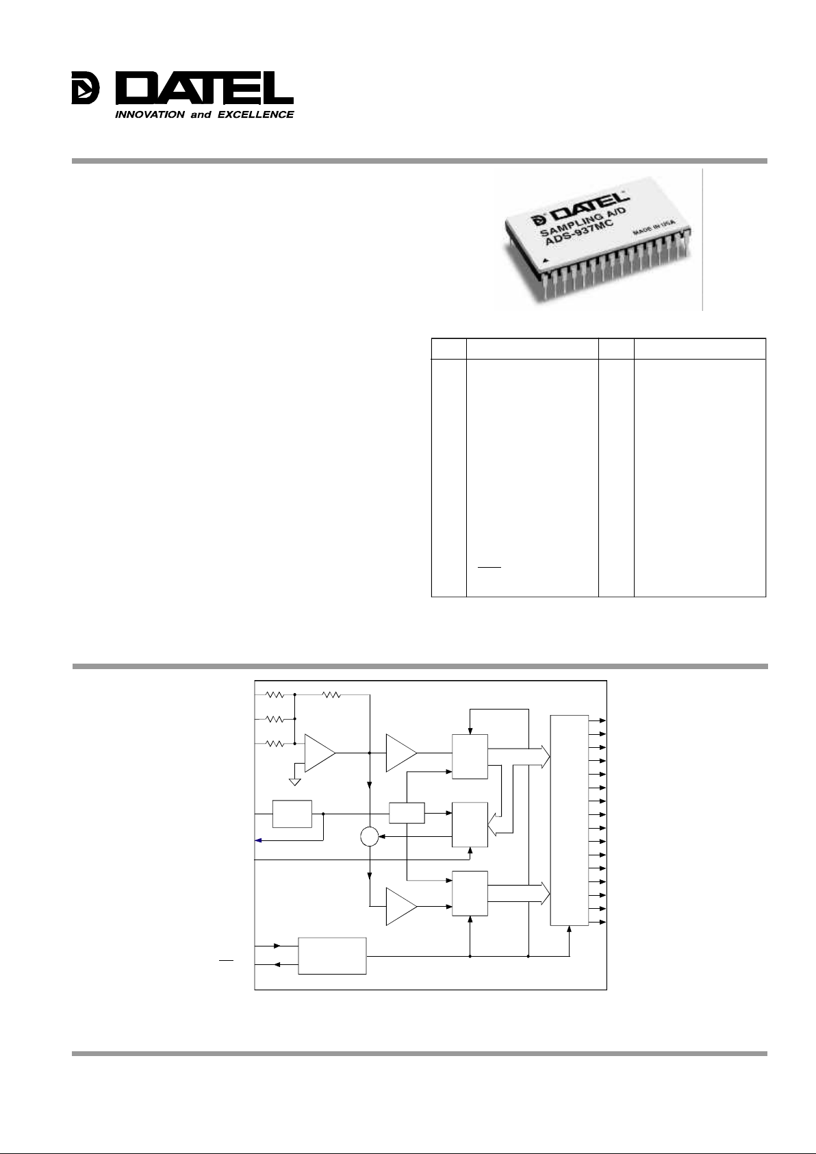
ADS-937
16-Bit, 1MHz, Low-Power
Sampling A/D Converters
GENERAL DESCRIPTION
The low-cost ADS-937 is a 16-bit, 1MHz sampling A/D converter. This device accurately samples full-scale input signals
up to Nyquist frequencies with no missing codes. This feature,
combined with excellent signal-to-noise ratio (SNR) and total
harmonic distortion (THD), makes the ADS-937 the ideal
choice for both time-domain (CCD/medical imaging, scanners,
process control) and frequency-domain (radar, telecommunications, spectrum analysis) applications.
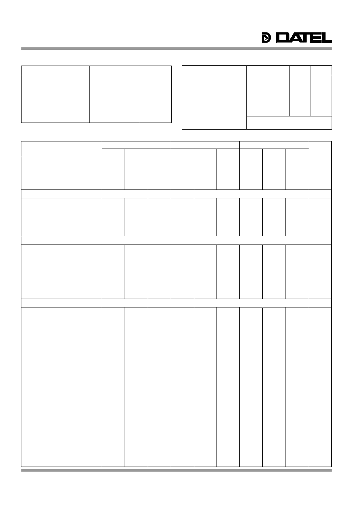
Packaged in a 32-pin, side-brazed, metal-sealed, ceramic
TDIP, the functionally complete ADS-937 contains a fastsettling sample-hold amplifier, a subranging (two-pass) A/D
converter, an internal reference, timing/control logic, and errorcorrection circuitry. Digital input and output levels are TTL.
ADS-937 only requires the rising edge of the start convert
pulse to operate.
Requiring ±15V and ±5V supplies, the ADS-937 typically
dissipates 1.25 Watts. The device is offered with both bipolar
(±5V) and unipolar (0 to –10V) analog input ranges. Models
are available for use in either commercial (0 to +70°C) or
INPUT/OUTPUT CONNECTIONS
Figure 1. ADS-937 Functional Block Diagram
1 ANALOG INPUT 32 BIT 1 (MSB)
2 ANALOG GROUND 31 BIT 2
3 UNIPOLAR 30 BIT 3
4 OFFSET ADJUST 29 BIT 4
5 +5V REFERENCE OUT 28 BIT 5
6 GAIN ADJUST 27 BIT 6
7 COMPENSATION 26 BIT 7
8 –15V SUPPLY 25 BIT 8
9 +15V SUPPLY 24 BIT 9
10 +5V ANALOG SUPPLY 23 BIT 10
11 –5V ANALOG SUPPLY 22 BIT 11
12 ANALOG GROUND 21 BIT 12
13 DIGITAL GROUND 20 BIT 13
14 +5V DIGITAL SUPPLY 19 BIT 14
15 EOC 18 BIT 15
16 START CONVERT 17 BIT 16 (LSB)
PIN FUNCTION PIN FUNCTION
REF
DAC
32 BIT 1 (MSB)
31 BIT 2
30 BIT 3
29 BIT 4
28 BIT 5
27 BIT 6
26 BIT 7
25 BIT 8
24 BIT 9
23 BIT 10
22 BIT 11
21 BIT 12
20 BIT 13
19 BIT 14
18 BIT 15
17 BIT 16 (LSB)
TIMING AND
CONTROL LOGIC
ANALOG INPUT 1
START CONVERT 16
EOC 15
–
+
S/H
BUFFER
DIGITAL CORRECTION LOGIC
FLASH
ADC
1
FLASH
ADC
2
Σ
AMP
GAIN
CIRCUIT
COMPENSATION 7
+5V REFERENCE OUT 5
10
+5V ANALOG
SUPPLY
11
–5V ANALOG
SUPPLY
2, 12
ANALOG
GROUND
14
+5V DIGITAL
SUPPLY
9
+15V
SUPPLY
8
–15V
SUPPLY
13
DIGITAL
GROUND
OFFSET ADJUST 4
UNIPOLAR 3
GAIN ADJUST 6
DATEL, Inc., Mansfield, MA 02048 (USA) • Tel: (508) 339-3000, (800) 233-2765 Fax: (508) 339-6356 • Email: sales@datel.com • Internet: www.datel.com
® ®
Page 2
ADS-937
2
® ®
+25°C 0 to +70°C –55 to +125°C
ANALOG INPUTS MIN. TYP. MAX. MIN. TYP. MAX. MIN. TYP. MAX. UNITS
Input Voltage Ranges ➁
Bipolar — ±5 — — ±5 — — ±5 — Volts
Unipolar — 0 to –10 — — 0 to –10 — — 0 to –10 — Volts
Input Resistance — 1 — — 1 — — 1 — kΩ
Input Capacitance — 7 15 — 7 15 — 7 15 pF
DIGITAL INPUTS
Logic Levels
Logic "1" +2.0 — — +2.0 — — +2.0 — — Volts
Logic "0" — — +0.8 — — +0.8 — — +0.8 Volts
Logic Loading "1" — — +20 — — +20 — — +20 µA
Logic Loading "0" — — –20 — — –20 — — –20 µA
Start Convert Positive Pulse Width ➂ 20 500 — 20 500 — 20 500 — ns
STATIC PERFORMANCE
Resolution — 16 — — 16 — — 16 — Bits
Integral Nonlinearity — ±0.75 — — ±1.5 — — ±2 — LSB
Differential Nonlinearity (f
in = 10kHz) –0.95 ±0.5 +1 –0.95 ±0.5 +1 –0.95 ±0.5 +1.5 LSB
Full Scale Absolute Accuracy — ±0.1 ±0.25 — ±0.2 ±0.4 — ±0.25 ±0.5 %FSR
Bipolar Zero Error (Tech Note 2) — ±0.1 ±0.15 — ±0.1 ±0.25 — ±0.15 ±0.5 %FSR
Bipolar Offset Error (Tech Note 2) — ±0.1 ±0.2 — ±0.15 ±0.3 — ±0.2 ±0.5 %FSR
Gain Error (Tech Note 2) — ±0.1 ±0.3 — ±0.25 ±0.5 — ±0.4 ±0.7 %
Unipolar Offset Error (Tech Note 2) — ±0.1 ±0.15 — ±0.1 ±0.25 — ±0.15 ±0.5 %FSR
No Missing Codes (f
in = 10kHz) 16 — — 16 — — 16 — — Bits
DYNAMIC PERFORMANCE
Peak Harmonics (–0.5dB)
dc to 100kHz — –90 –84 — –90 –84 — –88 –83 dB
100kHz to 500kHz — –88 –81 — –88 –81 — –87 –80 dB
Total Harmonic Distortion (–0.5dB)
dc to 100kHz — –87 –82 — –87 –82 — –86 –81 dB
100kHz to 500kHz — –86 –81 — –86 –81 — –85 –80 dB
Signal-to-Noise Ratio
(w/o distortion, –0.5dB)
dc to 100kHz 85 88 — 85 88 — 84 87 — dB
100kHz to 500kHz 84 87 — 84 87 — 83 87 — dB
Signal-to-Noise Ratio ➃
(& distortion, –0.5dB)
dc to 100kHz 81 85 — 81 85 — 80 84 — dB
100kHz to 500kHz 80 84 — 80 84 — 78 83 — dB
Noise — 110 — — 110 — — 110 — µVrms
Two-Tone Intermodulation
Distortion (f
in = 100kHz,
240kHz, f
s = 1MHz, –0.5dB) — –85 — — –85 — — –85 — dB
Input Bandwidth (–3dB)
Small Signal (–20dB input) — 4.5 — — 4.5 — — 4.5 — MHz
Large Signal (–0.5dB input) — 4 — — 4 — — 4 — MHz
Feedthrough Rejection (f
in = 500kHz) — 84 — — 84 — — 84 — dB
Slew Rate — ±33 — — ±33 — — ±33 — V/µs
Aperture Delay Time — +20 — — +20 — — +20 — ns
Aperture Uncertainty — 5 — — 5 — — 5 — ps rms
S/H Acquisition Time
( to ±0.003%FSR, 10V step) — 260 300 — 260 300 — 260 300 ns
Overvoltage Recovery Time ➄ — 500 1000 — 500 1000 — 500 1000 ns
A/D Conversion Rate 1 — — 1 — — 1 — — MHz
PARAMETERS LIMITS UNITS
+15V Supply (Pin 9) 0 to +16 Volts
–15V Supply (Pin 8) 0 to –16 Volts
+5V Supply (Pins 10, 14) 0 to +6 Volts
–5V Supply (Pin 11) 0 to –6 Volts
Digital Input (Pin 16) –0.3 to +V
DD +0.3 Volts
Analog Input (Pin 1) ±15 Volts
Lead Temperature (10 seconds) +300 °C
PARAMETERS MIN. TYP. MAX. UNITS
Operating Temp. Range, Case
ADS-937MC 0 — +70 °C
ADS-937MM/883 –55 — +125 °C
Thermal Impedance
θjc — 5 — °C/Watt
θca — 22 — °C/Watt
Storage Temperature Range –65 — +150 °C
Package Type 32-pin,side-brazed, metal-sealed, ceramic TDIP
Weight 0.56 ounces (16 grams)
ABSOLUTE MAXIMUM RATINGS
PHYSICAL/ENVIRONMENTAL
FUNCTIONAL SPECIFICATIONS
(TA = +25°C, ±VCC = ±15V, ±VDD = ±5V, 1MHz sampling rate, and a minimum 1 minute warm-up ➀ unless otherwise specified.)
Page 3
ADS-937
3
® ®
+25°C 0 to +70°C –55 to +125°C
ANALOG OUTPUT MIN. TYP. MAX. MIN. TYP. MAX. MIN. TYP. MAX. UNITS
Internal Reference
Voltage +4.95 +5.0 +5.05 +4.95 +5.0 +5.05 +4.95 +5.0 +5.05 Volts
Drift — ±30 — — ±30 — — ±30 — ppm/°C
External Current — 1 — — 1 — — 1 — mA
DIGITAL OUTPUTS
Logic Levels
Logic "1" +2.4 — — +2.4 — — +2.4 — — Volts
Logic "0" — — +0.4 — — +0.4 — — +0.4 Volts
Logic Loading "1" — — –4 — — –4 — — –4 mA
Logic Loading "0" — — +4 — — +4 — — +4 mA
Output Coding
Complementary Binary / Complementary Offset Binary
POWER REQUIREMENTS
Power Supply Ranges
+15V Supply +14.5 +15.0 +15.5 +14.5 +15.0 +15.5 +14.5 +15.0 +15.5 Volts
–15V Supply –14.5 –15.0 –15.5 –14.5 –15.0 –15.5 –14.5 –15.0 –15.5 Volts
+5V Supply +4.75 +5.0 +5.25 +4.75 +5.0 +5.25 +4.75 +5.0 +5.25 Volts
–5V Supply –4.75 –5.0 –5.25 –4.75 –5.0 –5.25 –4.75 –5.0 –5.25 Volts
Power Supply Currents
+15V Supply — +7 +9 — +7 +9 — +7 +9 mA
–15V Supply — –8 –10 — –8 –10 — –8 –10 mA
+5V Supply — +133 +145 — +133 +145 — +133 +145 mA
–5V Supply — –72 –80 — –72 –80 — –72 –80 mA
Power Dissipation — 1.25 1.35 — 1.25 1.35 — 1.25 1.35 Watts
Power Supply Rejection — — ±0.01 — — ±0.01 — — ±0.01 %FSR/%V
THERMAL REQUIREMENTS
All DATEL sampling A/D converters are fully characterized and
specified over operating temperature (case) ranges of 0 to
+70°C and –55 to +125°C. All room-temperature (T
A = +25°C)
production testing is performed without the use of heat sinks or
forced-air cooling. Thermal impedance figures for each device
are listed in their respective specification tables.
These devices do not normally require heat sinks, however,
standard precautionary design and layout procedures should be
used to ensure devices do not overheat. The ground and power
planes beneath the package, as well as all pcb signal runs to
and from the device, should be as heavy as possible to help
conduct heat away from the package. Electrically-insulating,
thermally-conductive "pads" may be installed underneath the
package. Devices should be soldered to boards rather than
"socketed", and of course, minimal air flow over the surface can
greatly help reduce the package temperature.
TECHNICAL NOTES
1. Obtaining fully specified performance from the ADS-937
requires careful attention to pc-card layout and power
supply decoupling. The device's analog and digital ground
systems are not connected to each other internally. For
optimal performance, tie all ground pins (2, 12 and 13)
directly to a large analog ground plane beneath the
package.
Bypass all power supplies and the +5V REFERENCE
OUTPUT (pin 5) to ground with 4.7µF tantalum capacitors in
parallel with 0.1µF ceramic capacitors. Locate the bypass
capacitors as close to the unit as possible. Tie a 47µF
capacitor between COMPENSATION (pin 7) and ground
(See figure 2.).
2. The ADS-937 achieves its specified accuracies without the
need for external calibration. If required, the device's small
initial offset and gain errors can be reduced to zero using
the adjustment circuitry shown in Figure 2. When using this
circuitry, or any similar offset and gain calibration hardware,
make adjustments following warm-up. To avoid interaction,
always adjust offset before gain. Float pins 4 and 6 if not
using offset and gain adjust circuits.
Footnotes:
➄ This is the time required before the A/D output data is valid once the analog input
is back within the specified range.
6.02
(SNR + Distortion) – 1.76 + 20 log
Full Scale Amplitude
Actual Input Amplitude
➀ All power supplies must be on before applying a start convert pulse. All
supplies and the clock (START CONVERT) must be present during warm-up
periods. The device must be continuously converting during this time.
➁ Contact DATEL for other input voltage ranges.
➂ A 1MHz clock with a 500nsec positive pulse width (50% duty cycle) is used for
all production testing. Any duty cycle may be used as long as a minimum
positive pulse width of 20nsec is maintained. For applications requiring lower
sampling rates, clock frequencies less than 1MHz may be used.
➃ Effective bits is equal to:
3. Applying a start convert pulse while a conversion is in
progress (EOC = logic "1") will initiate a new and inaccurate
conversion cycle. Data for the interrupted and subsequent
conversions will be invalid.
Page 4

ADS-937
4
® ®
3. For a bipolar input - Adjust the offset potentiometer until the
output code flickers equally between 1000 0000 0000 0000
and 0111 1111 1111 1111.
For a unipolar input - Adjust the offset potentiometer until
all output bits are 0's and the LSB flickers between 0 and 1.
Gain Adjust Procedure
1. Apply –4.999771V to the ANALOG INPUT (pin 1) for
bipolar gain adjust or apply –9.999771V to pin 1 for
unipolar gain adjust.
2. For a unipolar input - Adjust the gain potentiometer until all
output bits are 1's and the LSB flickers between 1 and 0.
For a bipolar input - Adjust the gain potentiometer until all
output bits are 1's and the LSB flickers between 1 and 0.
3. To confirm proper operation of the device, vary the applied
input voltage to obtain the output coding listed in Table 2.
UNIPOLAR INPUT VOLTAGE INPUT RANGE BIPOLAR
SCALE 0 to –10V MSB LSB MSB LSB ±5V SCALE
–FS +1 LSB –9.999847 1111 1111 1111 1111 0000 0000 0000 0000 +4.999847 +FS –1 LSB
–7/8 FS –8.750000 1110 0000 0000 0000 0001 1111 1111 1111 +3.750000 +3/4 FS
–3/4 FS –7.500000 1100 0000 0000 0000 0011 1111 1111 1111 +2.500000 +1/2 FS
–1/2 FS –5.000000 1000 0000 0000 0000 0111 1111 1111 1111 +0.000000 0
–1/4 FS –2.500000 0100 0000 0000 0000 1011 1111 1111 1111 –2.500000 –1/2 FS
–1/8 FS –1.250000 0010 0000 0000 0000 1101 1111 1111 1111 –3.750000 –3/4 FS
–1 LSB –0.000153 0000 0000 0000 0001 1111 1111 1111 1110 –4.999847 –FS +1 LSB
0 0.000000 0000 0000 0000 0000 1111 1111 1111 1111 –5.000000 –FS
OUTPUT CODING
COMPLEMENTARY
BINARY
COMPLEMENTARY
OFFSET BINARY
Table 2. Output Coding
CALIBRATION PROCEDURE
Connect the converter per Table 1 for the appropriate input
voltage range. Any offset/gain calibration procedures should
not be implemented until the device is fully warmed up. To
avoid interaction, adjust offset before gain. The ranges of
adjustment for the circuits in Figure 2 are guaranteed to
compensate for the ADS-937's initial accuracy errors and may
not be able to compensate for additional system errors.
A/D converters are calibrated by positioning their digital
outputs exactly on the transition point between two adjacent
digital output codes. This is accomplished by connecting
LED's to the digital outputs and performing adjustments until
certain LED's "flicker" equally between on and off. Other
approaches employ digital comparators or microcontrollers to
detect when the outputs change from one code to the next.
For the ADS-937, offset adjusting is normally accomplished
when the analog input is 0 minus ½LSB (–76.3µV). See Table
2 for the proper bipolar and unipolar output coding.
Gain adjusting is accomplished when the analog input is at
nominal full scale minus 1½LSB's (–9.999771V for unipolar
and –4.999771V for bipolar).
Zero/Offset Adjust Procedure
1. Apply a train of pulses to the START CONVERT input
(pin 16) so that the converter is continuously converting.
2. For unipolar or bipolar zero/offset adjust, apply –76.3µV to
the ANALOG INPUT (pin 1).
INPUT VOLTAGE INPUT TIE
RANGE PIN TOGETHER
±5V Pin 1 Pins 2 and 3
0 to –10V Pin 1 Pins 3 and 5
Table 1. Input Connections
Page 5

ADS-937
5
® ®
Figure 3. ADS-937 Timing Diagram
Figure 2. Typical ADS-937 Connection Diagram
Scale is approximately 50ns per division.
START
CONVERT
INTERNAL S/H
N
N+1
500ns typ.
Acquisition Time
260ns typ.
740ns typ.
5ns typ.
EOC
65ns typ.
Conversion Time
730ns typ.
OUTPUT
DATA
Data N-2 Valid
980ns typ.
Hold
Data N-1 Valid
20ns typ.
20ns
Invalid Data
N
Note: Scale is approximately 50ns per division. Sampling Rate = 1MHz.
2
11
ADS-937
20k
Ω
10
32
31
30
29
28
27
26
25
24
23
22
21
20
19
18
17
BIT 1 (MSB)
BIT 2
BIT 3
BIT 4
BIT 5
BIT 6
BIT 7
BIT 8
BIT 9
BIT 10
BIT 11
BIT 12
BIT 13
BIT 14
BIT 15
BIT 16 (LSB)
+5V ANALOG
15
ANALOG
GROUND
ANALOG
GROUND
DIGITAL
GROUND
0.1µF
4.7µF
0.1µF
UNIPOLAR
+
4.7µF
+5V
REF. OUT
COMPENSATION
47µF
14
13
3
5
7
START CONVERT
+5V DIGITAL
–15V
+15V
OFFSET
ADJUST
GAIN
ADJUST
46
16
0.1µF
4.7µF
12
9
0.1µF
4.7µF
8
+ +
0.1µF
4.7µF
0.1µF
4.7µF
+
+
EOC
–5V ANALOG
+15V
–15V
ANALOG INPUT
1
Pin 5 (ADS-937)
10k
Ω
Page 6

ADS-937
6
® ®
ADS-937
® ®
Figure 4. FFT Analysis of ADS-937
Figure 5. ADS-937 Histogram and Differential Nonlinearity
Digital Output Code0
65,536
Number of Occurrences
0
65,536
– 0.50
Codes
DNL (LSB's)
0.63
0
–10
–20
–30
–40
–50
–60
–70
–80
–90
–100
–110
–120
–130
–140
–150
0 50050 100 150 200 250 300 350 400 450
kHz kHz kHz kHz kHz kHz kHz kHz kHz kHz
Frequency
(fs = 1MHz, fin = 480kHz, Vin = – 0.5dB, 16,384-point FFT)
Amplitude Relative to Full Scale (dB)
Page 7

ADS-937
7
®®
Figure 6. ADS-937 Evaluation Board
JPR3
"OFFSET ADJ."
"GAIN ADJ."
23
1
AMPLIFIER
OPTION
3
2
1
(MSB)
(LSB)
CONVERT
JPR2
+
+
+
10uF
1
2
3
4
5
6
7
8
9
10
11
12
13
14
15
16
17
18
19
20
21
22
23
24
25
26
27
28
29
30
31
32
AIN
AGND
UNIPOLAR
OFFSET ADJ.
REF. OUT
GAIN ADJ
COMP.
–15VA
+15VA
+5VA
-5VA
AGND
DGND
+5VD
EOC
(LSB) BIT16
(MSB) BIT1
BIT2
BIT3
BIT4
BIT5
BIT6
BIT7
BIT8
BIT9
BIT10
BIT11
BIT12
BIT13
BIT14
BIT15
ADS-937
+
+
+
14
7
3
2
1
8
10
9
11
13
12
6
5
4
14 8
71
+
+
7
6
3
2
2
1
1
3
5
7
9
11
13
15
17
19
21
23
25
27
29
31
33
2
4
6
8
10
12
14
16
18
20
22
24
26
28
32
1
12
13
14
15
16
17
18
19
20
10
11
9
8
7
6
5
4
3
2
34
1
12
13
14
15
16
17
18
19
20
10
11
9
8
7
6
5
4
3
2
30
1D2D3D4D5D6D7D8DLE
1Q
2Q3Q4Q5Q6Q7Q8Q
OC
1D2D3D4D5D6D7D8DLE
1Q
2Q3Q4Q5Q6Q7Q8Q
OC
C26
C27
C29
C24
U3
U3
U3
4
R6
P3
U3
X1
C10
C21
C9
C7
C18
C6
C5
C15
C4
C28
C25
SG3
SG4
C11
R1
C22
AR1
R2
SG1
SG2
C3
C2
C1
P2P2P2P2P2P2P2P2P2P2P2P2P2P2P2P2P2P2P2P2P2P2P2P2P2P2P2P2P2P2P2P2U1P2U2P2
OPT
START
BIT16
EOC
+5VD
+5VD
+15V
–15V
+15V
–15V
+15V
74HCT573
74HCT573
0.1uF
OPT
10uF
10uF
51
0.1uF
10uF
0.1uF
0.1uF
10uF
0.1uF
0.1uF
10uF
0.1uF
0.1uF
0.1uF
OPT
OPT
OPT
OPT
0.1uF
0.1uF
0.1uF
EXT CLK
BIT15
BIT14
BIT13
BIT12
BIT11
BIT10
BIT9
BIT8
BIT7
BIT6
BIT5
BIT4
BIT3
BIT2
BIT1
AIN
–
4
+
C12
C23
–15V
OPT
OPT
REF
JPR2
R5
20K
R4
20K
C16
22uF
C14 22uF
C17
10uF
C20
+
+5VD
R3
10
N.C.
N.C.
N.C.
P1
26
24
25
23
2119171513
11
22
2018161412
10
864
21
3
975
+5V
+15V
–15V
–5V
+5VD
START
CONVERT
+5VD
+5VD
UUT
+
C19
C8
+5VA
10uF
0.1uF
+
+
Page 8

ADS-937
® ®
DATEL makes no representation that the use of its products in the circuits described herein, or the use of other technical information contained herein, will not infringe upon existing or future patent rights. The descriptions contained
herein do not imply the granting of licenses to make, use, or sell equipment constructed in accordance therewith. Specifications are subject to change without notice. The DATEL logo is a registered DATEL, Inc. trademark.
DS-0306C 5/99
MECHANICAL DIMENSIONS INCHES (mm)
ORDERING INFORMATION
OPERATING 32-PIN
MODEL NUMBER TEMP. RANGE PACKAGE
ADS-937MC 0 to +70°C TDIP
ADS-937MM –55 to +125°C TDIP
ADS-937/883 –55 to +125°C TDIP
ACCESSORIES
ADS-B937 Evaluation Board (without ADS-937)
Receptacles for pc board mounting can be ordered through AMP, Inc., Part # 3-331272-8
(Component Lead Socket), 32 required. For availability of MIL-STD-883 product, contact DATEL.
ISO 9001
ISO 9001
REGISTERED
DATEL, Inc. 11 Cabot Boulevard, Mansfield, MA 02048-1151
Tel: (508) 339-3000 (800) 233-2765 Fax: (508) 339-6356
Internet: www.datel.com Email: sales@datel.com
Data Sheet Fax Back: (508) 261-2857
DATEL (UK) LTD. Tadley, England Tel: (01256)-880444
DATEL S.A.R.L. Montigny Le Bretonneux, France Tel: 01-34-60-01-01
DATEL GmbH München, Germany Tel: 89-544334-0
DATEL KK Tokyo, Japan Tel: 3-3779-1031, Osaka Tel: 6-354-2025
® ®
Figure 7. ADS-937 Grounded Input Histogram
This histogram represents the typical
peak-to- peak noise (including quantization noise) associated with the ADS-937.
Digital Output Code
0.00
4000
3000
2000
1000
5000
1.62 MAX.
(41.15)
0.92 MAX.
(23.37)
0.018 TYP.
(0.46)
1.50 TYP
(38.10)
0.100 TYP.
(2.54)
0.05 TYP.
(1.27)
0.175 TYP
(4.45)
0.05 TYP.
(1.27)
0.220 TYP.
(6.86)
0.90 TYP.
(22.86)
0.010 TYP.
(0.254)
Dimension Tolerances
(unless otherwise indicated):
2 place decimal (.XX) ±0.010 (±0.254)
3 place decimal (.XXX) ±0.005 (±0.127)
Lead Material: Kovar Alloy
Lead Finish: 50 microinches (minimum)
gold plating over 100 microinches
(nominal) nickel plating
PIN 1 INDEX
0.05 TYP.
(1.27)
SEATING PLANE
 Loading...