

Datasheet ADS7861EB-2K5, ADS7861EB, ADS7861E-2K5, ADS7861 Datasheet (Burr Brown Corporation)
Page 1
Dual, 500kHz, 12-Bit, 2 + 2 Channel,
Simultaneous Sampling
ANALOG-TO-DIGITAL CONVERTER
FEATURES
● 4 INPUT CHANNELS
● FULLY DIFFERENTIAL INPUTS
● 2µs TOTAL THROUGHPUT PER CHANNEL
● GUARANTEED NO MISSING CODES
● 1MHz EFFECTIVE SAMPLING RATE
● LOW POWER: 40mW
● SSI SERIAL INTERFACE
APPLICATIONS
● MOTOR CONTROL
● MULTI-AXIS POSITIONING SYSTEMS
● 3-PHASE POWER CONTROL
DESCRIPTION
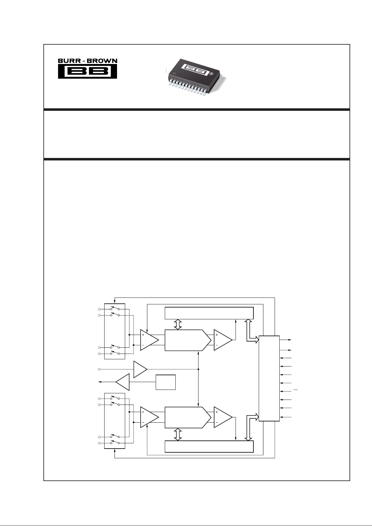
The ADS7861 is a dual, 12-bit, 500kHz, analog-todigital converter with 4 fully differential input channels
grouped into two pairs for high speed, simultaneous
signal acquisition. Inputs to the sample-and-hold amplifiers are fully differential and are maintained differential to the input of the A/D converter. This provides
excellent common-mode rejection of 80dB at 50kHz
which is important in high noise environments.
The ADS7861 offers a high speed, dual serial interface
and control inputs to minimize software overhead. The
output data for each channel is available as a 12-bit
word. The ADS7861 is offered in a 24-lead SSOP
package and is fully specified over the –40°C to +85°C
operating range.
®
ADS7861
© 1998 Burr-Brown Corporation PDS-1508A Printed in U.S.A. December, 1998
International Airport Industrial Park • Mailing Address: PO Box 11400, Tucson, AZ 85734 • Street Address: 6730 S. Tucson Blvd., Tucson, AZ 85706 • Tel: (520) 746-1111
Twx: 910-952-1111 • Internet: http://www.burr-brown.com/ • Cable: BBRCORP • Telex: 066-6491 • FAX: (520) 889-1510 • Immediate Product Info: (800) 548-6132
ADS7861
SAR
Serial
Interface
COMP
CLOCK
A0
M1
M0
CONVST
CS
RD
BUSY
SERIAL DATA B
SERIAL DATA A
CDAC
Internal
2.5V
Reference
SHA
CH A0–
CH A0+
REF
IN
CH A1–
CH A1+
SAR
COMP
CDAC
SHA
CH B0–
CH B0+
CH B1–
CH B1+
REF
OUT
Page 2
2
ADS7861
®
SPECIFICATIONS
All specifications T
MIN
to T
MAX
, +VA + VD = +5V, and V
REF
= internal +2.5V, f
CLK
= 8MHz, f
SAMPLE
= 500kHz, unless otherwise noted.
The information provided herein is believed to be reliable; however, BURR-BROWN assumes no responsibility for inaccuracies or omissions. BURR-BROWN assumes
no responsibility for the use of this information, and all use of such information shall be entirely at the user’s own risk. Prices and specifications are subject to change
without notice. No patent rights or licenses to any of the circuits described herein are implied or granted to any third party. BURR-BROWN does not authorize or warrant
any BURR-BROWN product for use in life support devices and/or systems.
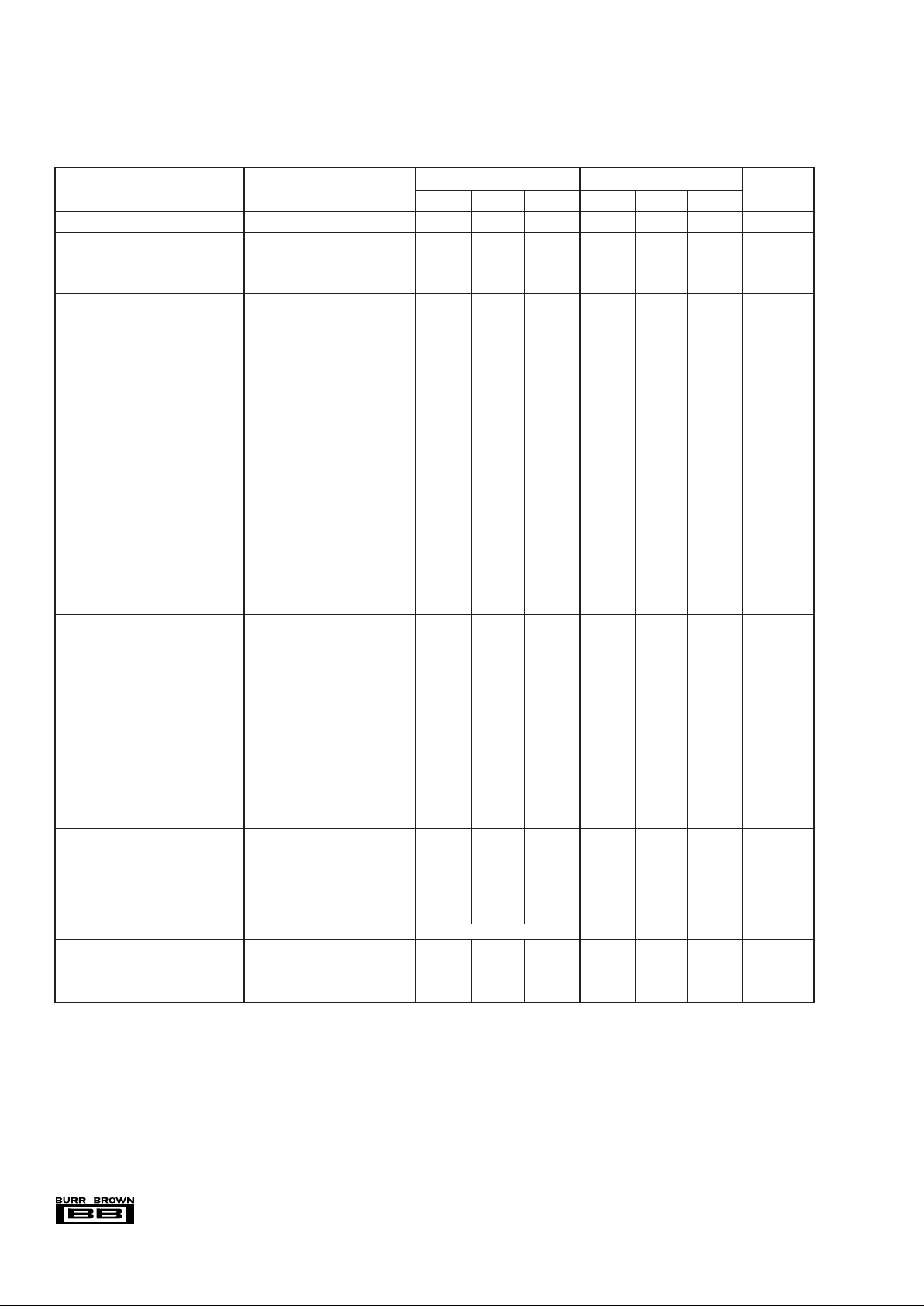
ADS7861E ADS7861EB
PARAMETER CONDITIONS MIN TYP MAX MIN TYP MAX UNITS
RESOLUTION 12 ✻ Bits
ANALOG INPUT
Input Voltage Range-Bipolar V
CENTER
= Internal V
REF
at 2.5V –V
REF
+V
REF
✻✻V
Input Capacitance 15 ✻ pF
Input Leakage Current ±1 ✻ µA
SYSTEM PERFORMANCE
No Missing Codes 12 ✻ Bits
Integral Linearity ±0.75 ±2 ±0.5 ±1 LSB
Integral Linearity Match 0.5 ±1 ✻✻ LSB
Differential Linearity ±1 ±0.5 ±1 LSB
Bipolar Offset Error Referenced to REF
IN
±0.5 ±3 ✻✻ LSB
Bipolar Offset Error Match 3 2 LSB
Positive Gain Error Referenced to REF
IN
±0.15 ±0.75 ±0.10 ±0.50 % of FSR
Positive Gain Error Match 2 1 LSB
Negative Gain Error Referenced to REF
IN
±0.15 ±0.75 ±0.10 ±0.50 % of FSR
Negative Gain Error Match 2 1 LSB
Common-Mode Rejection Ratio At DC 80 ✻ dB
V
IN
= ±1.25Vp-p at 50kHz 80 ✻ dB
Noise 120 ✻ µVrms
Power Supply Rejection Ratio 0.5 2 ✻✻ LSB
SAMPLING DYNAMICS
Conversion Time per A/D 1.625 ✻ µs
Acquisition Time 0.375 ✻ µs
Throughput Rate 500 ✻ kHz
Aperture Delay 3.5 ✻ ns
Aperture Delay Matching 100 ✻ ps
Aperture Jitter 50 ✻ ps
Small-Signal Bandwidth 40 ✻ MHz
DYNAMIC CHARACTERISTICS
Total Harmonic Distortion V
IN
= ±2.5Vp-p at 100kHz –72 –76 dB
SINAD V
IN
= ±2.5Vp-p at 100kHz 70 ✻ dB
Spurious Free Dynamic Range V
IN
= ±2.5Vp-p at 100kHz 72 76 dB
Channel-to-Channel Isolation V
IN
= ±2.5Vp-p at 100kHz –80 ✻ dB
VOLTAGE REFERENCE
Internal 2.475 2.5 2.525 ✻✻✻ V
Internal Drift ±25 ✻ ppm/°C
Internal Noise 50 ✻ µVp-p
Internal Source Current 2 ✻ mA
Internal Load Rejection 0.005 ✻ mV/µA
Internal PSRR 80 ✻ dB
External Voltage Range 1.2 2.5 2.6 ✻✻✻ V
Input Current 0.05 1 ✻✻ µA
Input Capacitance 5 ✻ pF
DIGITAL INPUT/OUTPUT
Logic Family CMOS ✻
Logic Levels: V
IH
IIH = +5µA 3.0
+VDD + 0.3
✻✻V
V
IL
IIL = +5µA –0.3 1 ✻✻V
V
OH
IOH = 2 CMOS Loads 3.5 ✻ V
V
OL
IOL = 2 CMOS Loads 0.4 ✻ V
External Clock, Optional 0.2 8 ✻✻MHz
Data Format Binary Two’s Complement ✻
POWER SUPPLY REQUIREMENTS
Power Supply Voltage, +V 4.75 5 5.25 ✻✻✻ V
Quiescent Current, +V
A
58 ✻✻ mA
Power Dissipation 25 40 ✻✻ mW
✻ Specifications same as ADS7861E.
Page 3
3
ADS7861
®
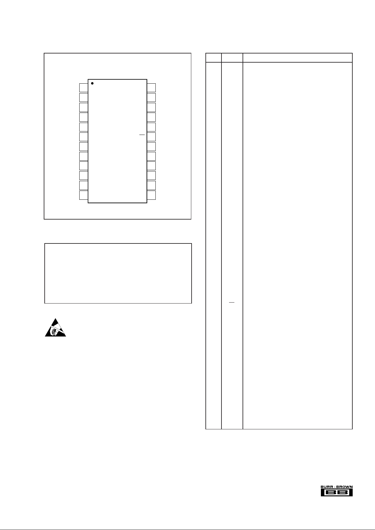
PIN NAME DESCRIPTION
1 DGND
Digital Ground. Connect directly to analog ground (pin 12).
2 CH B1+ Non-Inverting Input Channel B1
3 CH B1– Inverting Input Channel B1
4 CH B0+ Non-Inverting Input Channel B0
5 CH B0– Inverting Input Channel B0
6 CH A1+ Non-Inverting Input Channel A1
7 CH A1– Inverting Input Channel A1
8 CH A0+ Non-Inverting Input Channel A0
9 CH A0– Inverting Input Channel A0
10 REF
IN
Reference Input
11 REF
OUT
2.5V Reference Output
12 AGND
Analog Ground. Connect directly to digital ground (pin 1).
13 +VAAnalog Power Supply, +5VDC. Connect directly to digital
power supply (pin 24). Decouple to analog ground with a
0.1µF ceramic capacitor and a 10µF tantalum capacitor.
14 M1 Selects between the Serial Outputs. When M1 is LOW,
both Serial Output A and Serial Output B are selected for
data transfer. When M1 is HIGH, Serial output A is
configured for both Channel A data and Channel B data;
Serial Output B goes into tri-state (i.e., high impedance).
15 M0 Selects between two-channel and four-channel opera-
tion. When M0 is LOW, two-channel operation is se-
lected and operates in conjunction with A0. When A0 is
HIGH, Channel A1 and Channel B1 are being con-
verted. When A0 is LOW, Channel A0 and Channel B0
are being converted. When M0 is HIGH, four-channel
operation is selected. In this mode, all four channels are
converted in sequence starting with Channels A0 and
B0, followed by Channels A1 and B1.
16 A0 A0 operates in conjunction with M0. With M0 LOW and
A0 HIGH, Channel A1 and Channel B1 are converted.
With M0 LOW and A0 LOW, Channel A0 and Channel
B0 are converted.
17 CONVST Convert Start. When CONVST switches from LOW to
HIGH, the device switches from the sample to hold
mode, independent of the status of the external clock.
18 RD Synchronization Pulse for the Serial Output.
19 CS Chip Select. When LOW, the Serial Output A and Serial
Output B outputs are active; when HIGH, the serial
outputs are tri-stated.
20 CLOCK An external CMOS-compatible clock can be applied to
the CLOCK input to synchronize the conversion process
to an external source. The CLOCK pin controls the
sampling rate by the equation: CLOCK = 16 • f
SAMPLE
.
21 BUSY BUSY goes HIGH during a conversion and returns LOW
after the third LSB has been transmitted on either the
Serial A or Serial B output pin.
22 SERIAL The Serial Output data word is comprised of channel
information and 12 bits of data. In operation, data is valid
on the falling edge of DCLOCK for 16 edges after the
trailing edge of the RD.
23 SERIAL The Serial Output data word is comprised of channel
information and 12 bits of data. In operation, data is valid
on the falling edge of DCLOCK for 16 edges after the
trailing edge of the RD. When M1 is HIGH, both Channel
A data and Channel B data are available.
24 +V
D
Digital Power Supply, +5VDC. Connect directly to pin
13. Must be ≤ +V
A
.
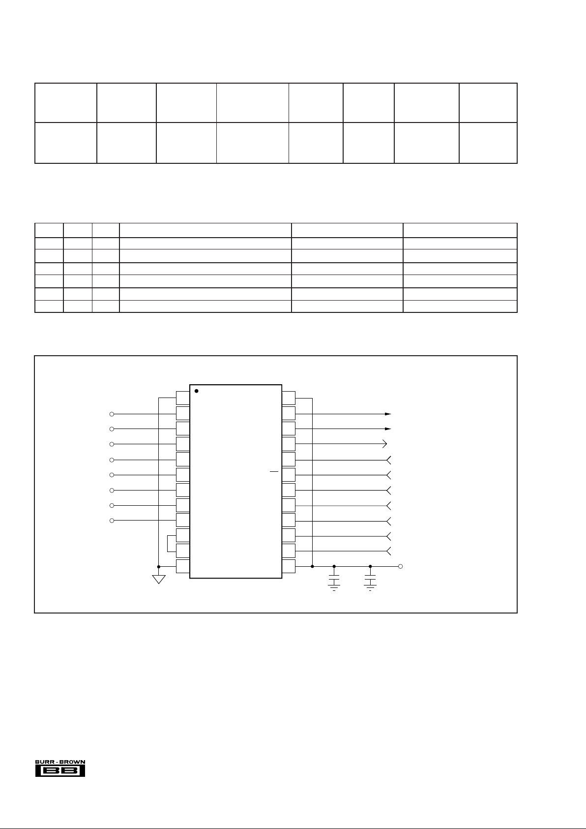
PIN CONFIGURATION
Top View SSOP
PIN DESCRIPTIONS
ABSOLUTE MAXIMUM RATINGS
Analog Inputs to AGND, Any Channel Input ........ –0.3V to (+VD + 0.3V)
REF
IN
..................................................................... –0.3V to (+VD + 0.3V)
Digital Inputs to DGND .......................................... –0.3V to (+V
D
+ 0.3V)
Ground Voltage Differences: AGND, DGND ................................... ±0.3V
+V
D
to AGND......................... –0.3V to +6V
Power Dissipation .......................................................................... 325mW
Maximum Junction Temperature................................................... +150°C
Operating Temperature Range ........................................ –40°C to +85°C
Storage Temperature Range .........................................–65°C to +150°C
Lead Temperature (soldering, 10s) ............................................... +300°C
ELECTROSTATIC
DISCHARGE SENSITIVITY
This integrated circuit can be damaged by ESD. Burr-Brown
recommends that all integrated circuits be handled with
appropriate precautions. Failure to observe proper handling and
installation procedures can cause damage.
ESD damage can range from subtle performance degradation to
complete device failure. Precision integrated circuits may be
more susceptible to damage because very small parametric
changes could cause the device not to meet its published specifications.
DATA
B
DATA
A
DGND
CH B1+
CH B1–
CH B0+
CH B0–
CH A1+
CH A1–
CH A0+
CH A0–
REF
IN
REF
OUT
AGND
1
2
3
4
5
6
7
8
9
10
11
12
24
23
22
21
20
19
18
17
16
15
14
13
+V
D
SERIAL DATA A
SERIAL DATA B
BUSY
CLOCK
CS
RD
CONVST
A0
M0
M1
+V
A
ADS7861
Page 4
4
ADS7861
®
MINIMUM
RELATIVE MAXIMUM SPECIFICATION PACKAGE
ACCURACY GAIN ERROR TEMPERATURE DRAWING ORDERING TRANSPORT
PRODUCT (LSB) (%) RANGE PACKAGE NUMBER
(1)
NUMBER
(2)
MEDIA
ADS7861E ±2 ±0.75 –40°C to +85°C 24-Lead SSOP 352 ADS7861E Rails
" " " " " " ADS7861EB/2K5 Tape and Reel
ADS7861EB ±1 ±0.5 –40°C to +85°C 24-Lead SSOP 352 ADS7861E Rails
" " " " " " ADS7861EB/2K5 Tape and Reel
NOTES: (1) For detailed drawing and dimension table, please see end of data sheet, or Appendix C of Burr-Brown IC Data Book. (2) Models with a slash (/) are
available only in Tape and Reel in the quantities indicated (e.g., /2K indicates 2000 devices per reel). Ordering 2000 pieces of “ADS7861E/2K” will get a single 2000piece Tape and Reel. For detailed Tape and Reel mechanical information, refer to Appendix B of Burr-Brown IC Data Book.
PACKAGE/ORDERING INFORMATION
BASIC CIRCUIT CONFIGURATION
M0 M1 A0 TWO-CHANNEL/FOUR-CHANNEL OPERATION DATA ON SERIAL OUTPUTS CHANNELS CONVERTED
0 0 0 Two Channel A and B A0, B0
0 0 1 Two Channel A and B A1, B1
0 1 0 Two Channel A Only A0, B0
0 1 1 Two Channel A Only A1, B1
1 0 X Four Channel A and B Sequential
1 1 X Four Channel A Only Sequential
X = Don’t Care.
TRUTH TABLE
DGND
CH B1+
CH B1–
CH B0+
CH B0–
CH A1+
CH A1–
CH A0+
CH A0–
REF
IN
REF
OUT
AGND
1
2
3
4
5
6
7
8
9
10
11
12
24
23
22
21
20
19
18
17
16
15
14
13
+V
D
SERIAL DATA A
SERIAL DATA B
BUSY
CLOCK
CS
RD
CONVST
A0
M0
M1
+V
A
BUSY Output
Clock Input
Chip Select
Read Input
Conversion Start
A0 Address Select
M0 Address Select
M1 Address Select
ADS7861
10µF
+
0.1µF
+5V Analog Supply
+
Page 5
5
ADS7861
®
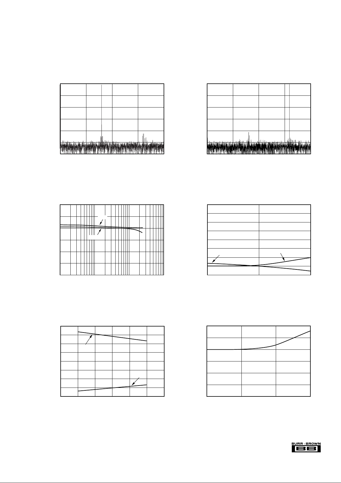
TYPICAL PERFORMANCE CURVES
At TA = +25°C, +VA + VD = +5V, and V
REF
= internal +2.5V, f
CLK
= 8MHz, f
SAMPLE
= 500kHz, unless otherwise noted.
FREQUENCY SPECTRUM
(4096 Point FFT; f
IN
= 99.9kHz, –0.5dB)
Frequency (kHz)
0
–20
–40
–60
–80
–100
–120
Amplitude (dB)
0 62.5 125 250187.5
FREQUENCY SPECTRUM
(4096 Point FFT; f
IN
= 199.9kHz, –0.5dB)
Frequency (kHz)
0
–20
–40
–60
–80
–100
–120
Amplitude (dB)
0 62.5 125 250187.5
CHANGE IN POSITIVE GAIN MATCH
vs TEMPERATURE
(Maximum Deviation for All Four Channels)
Temperature (°C)
0.6
0.5
0.4
0.3
0.2
0.1
0
Change in Positive Gain Match (LSB)
–40 25 85 150
CHANGE IN SIGNAL-TO-NOISE RATIO
AND SIGNAL-TO-(NOISE+DISTORTION)
vs TEMPERATURE
Temperature (°C)
0.7
0.6
0.5
0.4
0.3
0.2
0.1
0
–0.1
Delta from +25°C (dB)
–40 25 85
SNR
SINAD
CHANGE IN SPURIOUS FREE DYNAMIC RANGE
AND TOTAL HARMONIC DISTORTION
vs TEMPERATURE
Temperature (°C)
7
6
5
4
3
2
1
0
–1
+1
0
–0.5
–1
–1.5
–2
–2.5
–3
–3.5
SFDR Delta from +25°C (dB)
THD Delta from +25°C (dB)
–40 25 85
THD
SFDR
SIGNAL-TO-NOISE RATIO and
SIGNAL-TO-(NOISE+DISTORTION)
vs INPUT FREQUENCY
10k 100k1k 1M
Input Frequency (Hz)
SNR and SINAD (dB)
74
72
70
68
66
64
76
SINAD
SNR
Page 6

6
ADS7861
®
INTEGRAL LINEARITY ERROR vs CODE
Hex BTC Code
Typical of All Four Channels
1
0.75
0.5
0.25
0
–0.25
–0.5
–0.75
–1
ILE (LSB)
800 000 7FF
TYPICAL PERFORMANCE CURVES (CONT)
At TA = +25°C, +VA + VD = +5V, and V
REF
= internal +2.5V, f
CLK
= 8MHz, f
SAMPLE
= 500kHz, unless otherwise noted.
CHANGE IN NEGATIVE GAIN MATCH
vs TEMPERATURE
(Maximum Deviation for All Four Channels)
Temperature (°C)
0.2
0.18
0.16
0.14
0.12
0.1
0.08
0.06
0.04
0.02
0
Change in Negative Gain Match (LSB)
–40 25 85 150
CHANGE IN REFERENCE VOLTAGE
vs TEMPERATURE
Temperature (°C)
2.51
2.505
2.5
2.495
2.49
2.485
Change in Reference (V)
–40 25 85 150
CHANGE IN BIPOLAR ZERO
vs TEMPERATURE
Temperature (°C)
0.75
0.5
0.25
0
–0.25
–0.5
–0.75
Change in Bipolar Zero (LSB)
–40 25
A Channel
B Channel
85 150
CHANGE IN CMRR vs TEMPERATURE
Temperature (°C)
86
85
84
83
82
81
80
79
78
Change in CMRR (dB)
–40 –5 25 55 85
CHANGE IN BPZ MATCH vs TEMPERATURE
Temperature (°C)
1
0.75
0.5
0.25
0
Change in Bipolar Match (LSB)
–40 25 85 150
Page 7

7
ADS7861
®
DIFFERENTIAL LINEARITY ERROR vs CODE
Hex BTC Code
Typical of All Four Channels
1
0.75
0.5
0.25
0
–0.25
–0.5
–0.75
–1
DLE (LSB)
800 000 7FF
TYPICAL PERFORMANCE CURVES (CONT)
At TA = +25°C, +VA + VD = +5V, and V
REF
= internal +2.5V, f
CLK
= 8MHz, f
SAMPLE
= 500kHz, unless otherwise noted.
DIFFERENTIAL LINEARITY ERROR
vs TEMPERATURE
Temperature (°C)
0.8
0.6
0.4
0.2
0
–0.2
–0.4
–0.6
–0.8
DLE Error (LSB)
–40 25
Positive DLE
Negative DLE
85 150
INTEGRAL LINEARITY ERROR MATCH
vs CODE CHANNEL A0/CHANNEL A1
(Same Converter, Different Channels)
Hex BTC Code
0.25
0.2
0.15
0.1
0.05
0
–0.05
–0.1
–0.15
–0.2
–0.25
ILE (LSB)
800 000 7FF
INTEGRAL LINEARITY ERROR MATCH
vs CODE CHANNEL A0/CHANNEL B1
(Different Converter, Different Channels)
Hex BTC Code
0.25
0.2
0.15
0.1
0.05
0
–0.05
–0.1
–0.15
–0.2
–0.25
ILE (LSB)
800 000 7FF
INTEGRAL LINEARITY ERROR vs TEMPERATURE
Positive ILE
Negative ILE
Temperature (°C)
0.8
0.7
0.6
0.4
0.2
0
–0.2
–0.4
–0.6
–0.8
Change in ILE (LSB)
–40 25 85 150
INTEGRAL LINEARITY ERROR MATCH
vs TEMPERATURE
Channel A0/Channel B0
(Different Converter, Different Channels)
Temperature (°C)
0.47
0.46
0.45
0.44
0.43
0.42
0.41
0.40
0.39
0.38
Change in INL Match (LSB)
–40 25 85 150
Page 8

8
ADS7861
®
REFERENCE
Under normal operation, the REF
OUT
pin (pin 2) should be
directly connected to the REFIN pin (pin 1) to provide an
internal +2.5V reference to the ADS7862. The ADS7862
can operate, however, with an external reference in the range
of 1.2V to 2.6V for a corresponding full-scale range of 2.4V
to 5.2V.
The internal reference of the ADS7862 is double-buffered.
If the internal reference is used to drive an external load, a
buffer is provided between the reference and the load applied to pin 2 (the internal reference can typically source
2mA of current load—capacitance should not exceed 100pF).
If an external reference is used, the second buffer provides
isolation between the external reference and the CDAC.
This buffer is also used to recharge all of the capacitors of
both CDACs during conversion.
ANALOG INPUT
The analog input is bipolar and fully differential. There are
two general methods of driving the analog input of the
ADS7861: single-ended or differential (see Figures 1 and 2).
When the input is single-ended, the –IN input is held at the
common-mode voltage. The +IN input swings around the
same common voltage and the peak-to-peak amplitude is the
(common-mode +V
REF
) and the (common-mode –V
REF
).
The value of V
REF
determines the range over which the
common-mode voltage may vary (see Figure 3).
When the input is differential, the amplitude of the input is the
difference between the +IN and –IN input, or (+IN) – (–IN).
The peak-to-peak amplitude of each input is ±1/2V
REF
around
this common voltage. However, since the inputs are 180° out
of phase, the peak-to-peak amplitude of the differential voltage is +V
REF
to –V
REF
. The value of V
REF
also determines the
range of the voltage that may be common to both inputs (see
Figure 4).
INTRODUCTION
The ADS7861 is a high speed, low power, dual, 12-bit A/D
converter that operates from a single +5V supply. The input
channels are fully differential with a typical common-mode
rejection of 80dB. The part contains dual, 2µs successive
approximation ADCs, two differential sample-and-hold amplifiers, an internal +2.5V reference with REFIN and REF
OUT
pins and a high-speed parallel interface. The ADS7861
requires an external clock. In order to achieve the maximum
throughput rate of 500kHz, the master clock must be set at
8MHz. A minimum of 16 clock cycles are required for each
12-bit conversion.
There are four analog inputs that are grouped into two channels (A and B). Channel selection is controlled by the M0 (pin
14), M1 (pin 15) and A0 (pin 16) pins. Each channel has two
inputs (A0 and A1 and B0 and B1) that can be sampled and
converted simultaneously, thus preserving the relative phase
information of the signals on both analog inputs. The part
accepts an analog input voltage in the range of –V
REF
to
+V
REF
, centered around the internal +2.5V reference. The part
will also accept bipolar input ranges when a level shift circuit
is used at the front end (see Figure 7).
All conversions are initiated on the ADS7861 by bringing
the CONVST pin HIGH for a minimum of 15ns. CONVST
HIGH places both sample-and-hold amplifiers in the hold
state simultaneously and the conversion process is started on
both channels. The RD pin (pin 18) can be connected to
CONVST to simplify operation. Depending on the status of
the M0, M1 and A0 pins, the ADS7861 will (a) operate in
either two-channel or four-channel mode and (b) output data
on both the Serial A and Serial B output or both channels can
be transmitted on the A output only.
NOTE: See the Timing and Control section of this data sheet
for more information.
SAMPLE-AND-HOLD SECTION
The sample-and-hold amplifiers on the ADS7861 allow the
ADCs to accurately convert an input sine wave of full-scale
amplitude to 12-bit accuracy. The input bandwidth of the
sample-and-hold is greater than the Nyquist rate (Nyquist
equals one-half of the sampling rate) of the ADC even when
the ADC is operated at its maximum throughput rate of
500kHz. The typical small-signal bandwidth of the sampleand-hold amplifiers is 40MHz.
Typical aperture delay time or the time it takes for the
ADS7861 to switch from the sample to the hold mode
following the CONVST pulse is 3.5ns. The average delta of
repeated aperture delay values is typically 50pS (also known
as aperture jitter). These specifications reflect the ability of
the ADS7861 to capture AC input signals accurately at the
exact same moment in time.
ADS7861
ADS7861
Single-Ended Input
Common
Voltage
–V
REF
to +V
REF
peak-to-peak
Differential Input
Common
Voltage
V
REF
peak-to-peak
V
REF
peak-to-peak
FIGURE 1. Methods of Driving the ADS7861 Single-Ended
or Differential.
Page 9

9
ADS7861
®
FIGURE 3. Single-Ended Input: Common-Mode Voltage
Range vs V
REF
.
1.0 1.5
1.2
2.0 2.5
2.6
3.0
V
REF
(V)
Common Voltage Range (V)
–1
0
1
2
3
4
5
2.7
2.3
4.1
0.9
V
CC
= 5V
Single-Ended Input
Differential Input
1.0 1.5
1.2
2.0 2.5
2.6
3.0
V
REF
(V)
Common Voltage Range (V)
–1
0
1
2
3
4
5
4.7
0.3
V
CC
= 5V
4.05
0.90
FIGURE 2. Using the ADS7861 in the Single-Ended and Differential Input Modes.
FIGURE 4. Differential Input: Common-Mode Voltage
Range vs V
REF
.
In each case, care should be taken to ensure that the output
impedance of the sources driving the +IN and –IN inputs are
matched. Otherwise, this may result in offset error, gain
error and linearity error which will change with both temperature and input voltage.
The input current on the analog inputs depend on a number
of factors: sample rate, input voltage, and source impedance.
Essentially, the current into the ADS7861 charges the internal capacitor array during the sampling period. After this
capacitance has been fully charged, there is no further input
current. The source of the analog input voltage must be able
to charge the input capacitance (15pF) to a 12-bit settling
level within 2 clock cycles. When the converter goes into the
hold mode, the input impedance is greater than 1GΩ.
Care must be taken regarding the absolute analog input
voltage. The +IN input should always remain within the
range of GND – 300mV to VDD + 0.3V.
CM +V
REF
+V
REF
–V
REF
Single-Ended Inputs
t
+IN
CM
Voltage
CM
–VREF
CM +1/2V
REF
Differential Inputs
NOTES: Common-Mode Voltage (Differential Mode) = Common-Mode Voltage (Single-Ended Mode) = IN–.
(IN+) + (IN–)
2
The maximum differential voltage between +IN and –IN of the ADS7862 is V
REF
. See Figures 2 and 3 for a further
explanation of the common voltage range for single-ended and differential inputs.
t
+IN
–IN
CM
Voltage
CM
–1/2V
REF
–IN = CM Voltage
+V
REF
–V
REF
Page 10

10
ADS7861
®
Code (decimal)
8000
7000
6000
5000
4000
3000
2000
1000
0
Number of Conversions
2044 2045 2046 2047 2048
FIGURE 5. Histogram of 8,000 Conversions of a DC Input.
FIGURE 6. Test Circuits for Timing Specifications. FIGURE 7. Level Shift Circuit for Bipolar Input Ranges.
TRANSITION NOISE
Figure 5 shows a histogram plot for the ADS7861 following
8,000 conversions of a DC input. The DC input was set at
output code 2046. All but one of the conversions had an
output code result of 2046 (one of the conversions resulted
in an output of 2047). The histogram reveals the excellent
noise performance of the ADS7861.
BIPOLAR INPUTS
The differential inputs of the ADS7861 were designed to
accept bipolar inputs (–V
REF
and +V
REF
) around the internal
reference voltage (2.5V), which corresponds to a 0V to 5V
input range with a 2.5V reference. By using a simple op amp
circuit featuring a single amplifier and four external resistors, the ADS7861 can be configured to except bipolar
inputs. The conventional ±2.5V, ±5V, and ±10V input
ranges can be interfaced to the ADS7861 using the resistor
values shown in Figure 7.
TIMING AND CONTROL
The operation of the ADS7861 can be configured in four
different modes by using the address pins M0 (pin 14), M1
(pin 15) and A0 (pin 16).
The M0 pin selects between two- and four-channel operation
(in two-channel operation, the A0 pin selects between Channels 0 and 1; in four-channel operation the A0 pin is ignored
and the channels are switched automatically after each
conversion). The M1 pin selects between having serial data
transmitted simultaneously on both the Serial A data output
(pin 23) and the Serial B data output (pin 22) or having both
channels output data through the Serial A port. The A0 pin
selects either Channel 0 or Channel 1 (see Pin Descriptions
and Serial Output Truth Table for more information).
The next four sections will explain the four different modes
of operation.
Mode I (M0 = 0, M1 = 0)
With the M0 and M1 pins both set to ‘0’, the ADS7861 will
operate in two-channel operation (the A0 pin must be used
to switch between Channels A and B). A conversion is
initiated by bringing CONVST HIGH for a minimum of
15ns. It is very important that CONVST be brought HIGH
a minimum of 10ns prior to a rising edge of the external
clock or 5ns after the rising edge. If CONVST is brought
R
1
R
2
+IN
–IN
REF
OUT
(pin 2)
2.5V
4kΩ
20kΩ
Bipolar Input
BIPOLAR INPUT R
1
R
2
±10V 1kΩ 5kΩ
±5V 2kΩ 10kΩ
±2.5V 4kΩ 20kΩ
OPA132
ADS7861
DATA
1.4V
Test Point
3kΩ
100pF
C
LOAD
t
R
DATA
Voltage Waveforms for DATA Rise and Fall Times t
R
, and tF.
V
OH
V
OL
t
F
DESCRIPTION ANALOG INPUT
Full-Scale Input Span –V
REF
to +V
REF
(1)
Least Significant (–V
REF
to +V
REF
)/ 4096
(2)
Bit (LSB)
+Full Scale 4.99878V 0111 1111 1111 7FF
Midscale 2.5V 0000 0000 0000 000
Midscale – 1 LSB 2.49878V 1111 1111 1111 FFF
–Full Scale 0V 1000 0000 0000 800
NOTES: (1) –V
REF
to +V
REF
around V
REF
. With a 2.5V reference, this corre-
sponds to a 0V to 5V input span. (2) 1.22mV with a 2.5V reference.
TABLE I. Ideal Input Voltages and Output Codes.
DIGITAL OUTPUT
BINARY TWO’S COMPLEMENT
BINARY CODE HEX CODE
Page 11

11
ADS7861
®
FIGURE 8. Conversion Mode.
HIGH within this window, it is then uncertain as to when the
ADS7861 will initiate conversion (see Figure 8 for a more
detailed description). Sixteen clock cycles are required to
perform a single conversion. Immediately following
CONVST switching to HIGH, the ADS7861 will switch
from the sample mode to the hold mode asynchronous to the
external clock. The BUSY output pin will then go HIGH and
remain HIGH for the duration of the conversion cycle. On
the falling edge of the first cycle of the external clock, the
ADS7861 will latch in the address for the next conversion
cycle depending on the status of the A0 pin (HIGH =
Channel 1, LOW = Channel 0). The address must be selected
15ns prior to the falling edge of cycle one of the external
clock and must remain ‘held’ for 15ns following the clock
edge. For maximum throughput time, the CONVST and RD
pins should be tied together. CS must be brought LOW to
enable the two serial outputs. Data will be valid on the rising
edge of all 16 clock cycles per conversion. The first bit of
data will be a status flag for either Channel 0 or 1, the second
bit will be a second status flag for either Channel A or B.
The subsequent data will be MSB-first through the LSB,
followed by two zeros (see Table II and Figures 9 and 10).
SYMBOL DESCRIPTION MIN TYP MAX UNITS COMMENTS
t
CONV
Conversion Time 1.75 µs When T
CKP
= 125ns
t
ACQ
Acquisition Time 0.25 µs When T
CKP
= 125ns
t
CKP
Clock Period 125 5000 ns
t
CKL
Clock LOW 40 ns
t
CKH
Clock HIGH 40 ns
t
F
DOUT Fall Time 25 ns
t
R
DOUT Rise Time 30 ns
t
1
CONVST HIGH 15 ns
t
2
Address Setup Time 15 ns Address latched on falling edge of CLK cycle ‘2’
t
3
Address Hold Time 15
t
4
RD Setup Time 15 ns Before falling edge of CLOCK
t
5
RD to CS Hold Time 15 ns After falling edge of CLOCK
t
6
CONVST LOW 20 ns
t
7
RD LOW 20 ns
t
8
CS to Data Valid 25 ns
t
9
CLOCK to Data Valid Delay 30 ns Maximum delay following rising edge of CLOCK
t
10
Data Valid After CLOCK
(1)
1 ns Time data is valid after second rising edge of CLOCK
NOTE: (1) ‘n – 1’ data will remain valid 1ns after rising edge of next CLOCK cycle.
TIMING SPECIFICATIONS
CLOCK CYCLE 1 2 3 4 5 6 7 8 9 10 11 12 13 14 15 16
SERIAL DATA
CH0 OR CH1 CHA OR CHB
DB11 DB10 DB9 DB8 DB7 DB6 DB5 DB4 DB3 DB2 DB1 DB0 0 0
TABLE II. Serial Data Output Format.
NOTE: All CONVST commands which occur more than 10ns before the rising edge of cycle ‘1’ of the external clock
(Region ‘A’) will initiate a conversion on the rising edge of cycle ‘1’. All CONVST commands which occur 5ns after
the rising edge of cycle ‘1’ or 10ns before the rising edge of cycle 2 (Region ‘B’) will initiate a conversion on the
rising edge of cycle ‘2’. All CONVST commands which occur 5ns after the rising edge of cycle ‘2’ (Region ‘C’) will
initiate a conversion on the rising edge of the next clock period. The CONVST pin should never be switched from
LOW to HIGH in the region 10ns prior to the rising edge of the CLOCK and 5ns after the rising edge (gray areas). If
CONVST is toggled in this gray area, the conversion could begin on either the same rising edge of the CLOCK or
the following edge.
CLOCK
CONVST
Cycle 1 Cycle 2
t
CKP
125ns
10ns
5ns
10ns
5ns
A B C
Page 12

12
ADS7861
®
Mode II (M0 = 0, M1 = 1)
With M1 set to ‘1’, the ADS7861 will output data on the
Serial Data A pin only. All other pins function in the same
manner as Mode I except that the Serial Data B output will
tri-state (i.e., high impedance) after a conversion following
M1 going HIGH. Another difference in this mode involves
the CONVST pin. Since it takes 32 clock cycles to output
the results from both A/D converters (rather than 16 when
M1 = 0), the ADS7861 will take 4µs to complete a
conversion on both A/Ds. Therefore, every second CONVST
command will be ignored by the ADS7861 since it will
require two conversion cycles to transmit both channels
out the serial A port. See Figure 11.
Mode III (M0 = 1, M1 = 0)
With M0 set to ‘1’, the ADS7861 will cycle through Channels 0 and 1 sequentially (the A0 pin is ignored). At the same
time, setting M1 to ‘0’ places both Serial Outputs, A and B,
in the active mode. See Figure 12.
Mode IV (M0 = 1, M1 = 1)
Similar to Mode II, Mode IV uses the Serial A output line to
transmit data exclusively. Following the first conversion
after M1 goes HIGH, the serial B output will go into tristate. See Figure 13. As in Mode II, the second CONVST
command is always ignored when M1 = 1.
READING DATA
In all four timing diagrams, the CONVST pin and the RD
pins are tied together. If so desired, the two lines can be
separated. Data on the Serial Output pins (A and B) will
become valid following the third external clock cycle following a RD LOW. Refer to Table II for data output format.
LAYOUT
For optimum performance, care should be taken with the
physical layout of the ADS7861 circuitry. This is particularly true if the CLOCK input is approaching the maximum
throughput rate.
The basic SAR architecture is sensitive to glitches or sudden
changes on the power supply, reference, ground connections
and digital inputs that occur just prior to latching the output
of the analog comparator. Thus, driving any single conversion for an n-bit SAR converter, there are n “windows” in
which large external transient voltages can affect the conversion result. Such glitches might originate from switching
power supplies, nearby digital logic or high power devices.
The degree of error in the digital output depends on the
reference voltage, layout, and the exact timing of the external event. Their error can change if the external event
changes in time with respect to the CLOCK input.
With this in mind, power to the ADS7861 should be clean
and well bypassed. A 0.1µF ceramic bypass capacitor should
be placed as close to the device as possible. In addition, a
1µF to 10µF capacitor is recommended. If needed, an even
larger capacitor and a 5Ω or 10Ω series resistor may be used
to low pass filter a noisy supply. On average, the ADS7861
draws very little current from an external reference as the
reference voltage is internally buffered. However, glitches
from the conversion process appear at the V
REF
input and the
reference source must be able to handle this. Whether the
reference is internal or external, the V
REF
pin should be
bypassed with a 0.1µF capacitor. An additional larger capacitor may also be used, if desired. If the reference voltage
is external and originates from an op amp, make sure that it
can drive the bypass capacitor or capacitors without oscillation. No bypass capacitor is necessary when using the
internal reference (tie pin 10 directly to pin 11).
The GND pin should be connected to a clean ground point.
In many cases, this will be the ‘analog’ ground. Avoid
connections which are too near the grounding point of a
microcontroller or digital signal processor. If required, run a
ground trace directly from the converter to the power supply
entry point. The ideal layout will include an analog ground
plane dedicated to the converter and associated analog
circuitry.
APPLICATIONS
An applications section will be added featuring the ADS7862
interfacing to popular DSP processors. The updated data
sheet will be available in the near future on the Burr-Brown
web site:
http: //www.burr-brown.com/
Page 13

13
ADS7861
®
FIGURE 9. Mode I with Timing Specifications.
FIGURE 10. Mode I, Timing Diagram for M0 = 0 and M1 = 0.
A0
RD
CS
BUSY
SERIAL
DATA A
1CLOCK
CONVST
2345 768910111213141516123456
D11 D10 D9 D8 D7 D6 D5 D4 D3 D2 D1 D0 0 0 0 0 D11 D10 D9 D8
00
SERIAL
DATA B
D11 D10 D9 D8 D7 D6 D5 D4 D3 D2 D1 D0 0 0 0 0 D11 D10 D9 D800
t
3
t
1
t
CONV
Conversion 1 Start of Conversion 2
t
ACQ
t
CONV
t
7
t
10
t
9
t
6
t
CKH
t
CKL
0
t
2
t
4
t
8
t
5
1
CLOCK
CONVST
A0
RD
CS
SERIAL
DATA A
SERIAL
DATA B
BUSY
TIME 0 1µ 2µ 3µ 4µ 5µ 6µ
Time (seconds)
Conversion of Chx
12-Bit Data of Chx
12-Bit Data of Chx
12-Bit Data of ChA1
12-Bit Data of ChB1
Conversion of Ch0
16
CS HIGH, Outputs in Tri-State
Conversion of Ch1
A0 HIGH, Next Conversion: Ch1
A0 LOW, Next Conversion: Ch0
Conversion of Ch0
Conversion of Ch1
RD Connected to CONVST
Page 14

14
ADS7861
®
FIGURE 12. Mode III, Timing Diagram for M0 = 1 and M1 = 0.
FIGURE 11. Mode II, Timing Diagram for M0 = 0 and M1 = 1.
CLOCK
CONVST
A0
RD
M1
CS
SERIAL
DATA A
SERIAL
DATA B
BUSY
0TIME 5µ 10µ
Time (seconds)
M1 = 1 Serial Data B in Tri-state
C
h
B
C
h
A
C
h
B
C
h
A
Conversion of Chx
M1 = 1 and 1st CONVST
Conversion
A0 HIGH
Next Conversion Ch1
RD Connected with CONVST
12-Bit Data of ChAx
12-Bit Data of ChBx
M1 = 1 and 1st CONVST
Data of ChA
M1 = 1 and 2nd CONVST
Data of ChB
M1 = 1 and 1st CONVST
Data of ChA
M1 = 1 and 2nd CONVST
Data of ChB
Conversion of Chx
M1 = 1 and 1st CONVST
Conversion
M1 = 1 and 2nd CONVST
No Conversion
M1 = 1 and 1st CONVST
Conversion
M1 = 1 and 2nd CONVST
No Conversion
CS LOW Output Active
A0 LOW
Next Conversion Ch0
A0 LOW
Next Conversion Ch0
M1 = 1 and 2nd CONVST
No Conversion
M1 = 1 and 1st CONVST
Conversion
M1 = 1 and 2nd CONVST
No Conversion
161
M1 HIGH
Only Serial Data A Used as Output Starting with 1
st
Conversion
1
CLOCK
CONVST
A0
RD
M0
CS
SERIAL
DATA A
SERIAL
DATA B
BUSY
TIME 0 1µ 2µ 3µ 4µ 5µ 6µ
Time (seconds)
12-Bit Data of ChAx
12-Bit Data of ChBx
12-Bit Data of ChA0
12-Bit Data of ChB0 12-Bit Data of ChB1
C
h
1
12-Bit Data of ChA1
C
h
1
C
h
0
C
h
0
16
CS LOW, Output is Active
M0 = 1 A0 Ignored
4-Ch Operation and 1st Conversion Ch0 4-Ch Operation and 2nd Conversion Ch1
RD Connected with CONVST
M0 = 1, 4-Ch Operation Starts with Next Conversion
Page 15

15
ADS7861
®
FIGURE 13. Mode IV, Timing Diagram for M0 = 1 and M1 = 1.
CLOCK
CONVST
A0
RD
M0
CS
SERIAL
DATA A
SERIAL
DATA B
BUSY
0TIME 5µ 10µ
Time (seconds)
M1 = 1 Serial Data B in Tri-state
C
h
B
C
h
0
C
h
A
C
h
1
C
h
B
C
h
1
C
h
A
C
h
0
Conversion of Chx
M1 = 1 and 1st CONVST
Conversion
M0 HIGH
4-Ch Operation Starts, A0 Ignored
M0 HIGH
4-Ch Operation Starts
M0 = 1 and 1st Active CONVST
Ch0
M0 = 1 and 2nd Active CONVST
Ch1
M1
M1 HIGH
Only Serial Data A Used as Output Starting with 1
st
Conversion
RD Connected with CONVST
12-Bit Data of ChAx
12-Bit Data of ChBx
M1 = 1 and 1st CONVST
Data of ChA0
M1 = 1 and 2nd CONVST
Data of ChB0
M1 = 1 and 1st CONVST
Data of ChA1
M1 = 1 and 2nd CONVST
Data of ChB1
Conversion of Chx
M1 = 1 and 1st CONVST
Conversion
M1 = 1 and 2nd CONVST
No Conversion
M1 = 1 and 1st CONVST
Conversion
M1 = 1 and 2nd CONVST
No Conversion
CS LOW Output Active
M1 = 1 and 2nd CONVST
No Conversion
M1 = 1 and 1st CONVST
Conversion
M1 = 1 and 2nd CONVST
No Conversion
1 16
 Loading...