

Datasheet ADS7852YB-2K5, ADS7852YB-250, ADS7852Y-2K5, ADS7852 Datasheet (Burr Brown Corporation)
Page 1
1
®
ADS7852
ADS7852
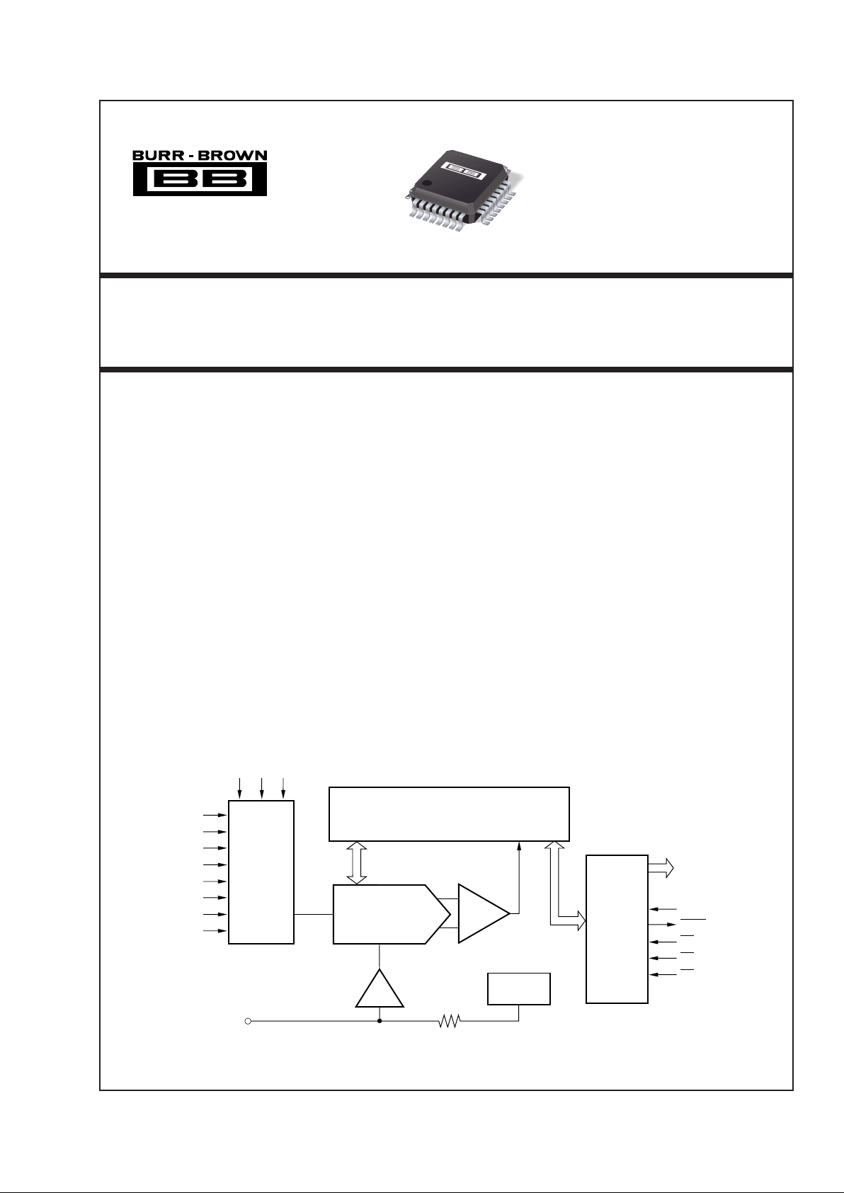
DESCRIPTION
The ADS7852 is an 8-channel, 12-bit analog-to-digital converter (A/D) complete with sample-and-hold,
internal 2.5V reference and a full 12-bit parallel output
interface. Typical power dissipation is 13mW at at
500kHz throughput rate. The ADS7852 features both
a nap mode and a sleep mode further reducing the
power consumption to 2mW. The input range is from
0V to twice the reference voltage. The reference voltage can be overdriven by an external voltage.
The ADS7852 is ideal for multi-channel applications
where low power and small size are critical. Medical
instrumentation, high-speed data acquisition and laboratory equipment are just a few of the applications that
would take advantage of the special features offered
by the ADS7852. The ADS7852 is available in an
TQFP-32 package and is fully specified and guaranteed over the –40°C to +85°C temperature range.
12-Bit, 8-Channel, Parallel Output
ANALOG-TO-DIGITAL CONVERTER
®
FEATURES
● 2.5V INTERNAL REFERENCE
● 8 INPUT CHANNELS
● 500kHz SAMPLING RATE
● SINGLE 5V SUPPLY
● ±1LSB: INL, DNL
● GUARANTEED NO MISSING CODES
● 70dB SINAD
● LOW POWER: 13mW
● TQFP-32 PACKAGE
APPLICATIONS
● DATA ACQUISITION
● TEST AND MEASUREMENT
● INDUSTRIAL PROCESS CONTROL
● MEDICAL INSTRUMENTS
©
1998 Burr-Brown Corporation PDS-1509C Printed in U.S.A. May, 2000
International Airport Industrial Park • Mailing Address: PO Box 11400, Tucson, AZ 85734 • Street Address: 6730 S. Tucson Blvd., Tucson, AZ 85706 • Tel: (520) 746-1111
Twx: 910-952-1111 • Internet: http://www.burr-brown.com/ • Cable: BBRCORP • Telex: 066-6491 • FAX: (520) 889-1510 • Immediate Product Info: (800) 548-6132
ADS7852
¤
For most current data sheet and other product
information, visit www.burr-brown.com
SAR
CDAC
ADS7852
Output
Latches
and
3-State
Drivers
Comparator
CLK
BUSY
WR
CS
RD
A0 A1 A2
8-Channel
MUX
Internal
+2.5V Ref
Buffer
V
REF
10kΩ
AIN0
AIN1
AIN2
AIN3
AIN4
AIN5
AIN6
AIN7
3-State
Parallel
Data Bus
Page 2
2
®
ADS7852
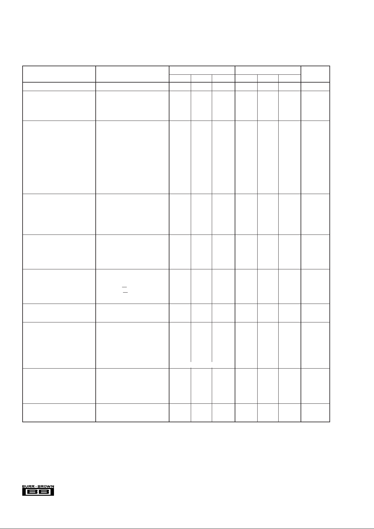
SPECIFICATIONS
At TA = –40°C to +85°C, fS = 500kHz, f
CLK
= 16 • fS, and VSS = +5V, using internal reference, unless otherwise specified.
ADS7852Y ADS7852YB
PARAMETER CONDITIONS MIN TYP MAX MIN TYP MAX UNITS
RESOLUTION 12 ✻ Bits
ANALOG INPUT
Input Voltage Range 0 5 ✻✻V
Input Impedance 5M ✻ Ω
Input Capacitance 15 ✻ pF
Input Leakage Current ±1 ✻ µA
DC ACCURACY
No Missing Codes 12 ✻ Bits
Integral Linearity Error ±2 ±1 LSB
(1)
Differential Linearity Error ±1 ±0.5 ±1 LSB
Offset Error ±2 ±5 ±1 ✻ LSB
Offset Error Drift ±4 ✻ ppm/°C
Offset Error Match ±1 ✻ LSB
Gain Error
(1)
Ext Ref = 2.5000V ±15 ±10 LSB
Gain Error Int Ref ±40 ±25 LSB
Gain Error Drift ±25 ✻ ppm/°C
Gain Error Match ±1 ✻ LSB
Noise 150 ✻ µVrms
Power Supply Rejection Ratio Worst-Case ∆, +V
SS
= 5V ±5% 1.2 ✻ LSB
SAMPLING DYNAMICS
Conversion Time 13.5 ✻ Clk Cycles
Acquisition Time 1.5 ✻ Clk Cycles
Throughput Rate 500 ✻ kHz
Multiplexer Settling Time 500 ✻ ns
Aperture Delay 5 ✻ ns
Aperture Jitter 30 ✻ ps
AC ACCURACY
Signal-to-Noise Ratio 72 ✻ dB
Total Harmonic Distortion
(3)
VIN = 5Vp-p at 50kHz –74 –72 –77 –76 dB
Signal-to-(Noise+Distortion) V
IN
= 5Vp-p at 50kHz 68 70 71 72 dB
Spurious Free Dynamic Range V
IN
= 5Vp-p at 50kHz 76 74 78 77 dB
Channel-to-Channel Isolation V
IN
= 5Vp-p at 50kHz 95 ✻ dB
REFERENCE OUTPUT
Internal Reference Voltage 2.48 2.50 2.52 ✻✻✻ V
Internal Reference Drift 30 ✻ ppm/°C
Input Impedance CS = GND 5 ✻ GΩ
CS = V
SS
5 ✻ GΩ
Source Current
(4)
Static Load 50 ✻ µA
REFERENCE INPUT
Range 2.0 2.55 ✻✻V
Resistance
(5)
to Internal Reference Voltage 10 ✻ kΩ
DIGITAL INPUT/OUTPUT
Logic Family CMOS ✻
Logic Levels:
V
IH
IIH = +5µA3+V
SS
+ 0.3 ✻✻V
V
IL
IIL = +5µA –0.3 0.8 ✻✻V
V
OH
IOH = 250µA 3.5 ✻ V
V
OL
IOL = 250µA 0.4 ✻ V
Data Format Straight Binary ✻
POWER SUPPLY REQUIREMENT
+V
SS
Specified Performance 4.75 5.25 ✻✻V
Quiescent Current 2.6 3.5 ✻✻ mA
Normal Power 13 17.5 ✻✻ mW
Nap Mode Current
(6)
600 800 ✻✻ µA
Sleep Mode Current
(6)
10 30 ✻✻ µA
TEMPERATURE RANGE
Specified Performance –40 +85 ✻✻°C
Storage –65 +150 ✻✻°C
✻ Specifications same as ADS7852Y.
NOTES: (1) LSB means Least Significant Bit, with V
REF
equal to +2.5V, one LSB is 1.22mV. (2) Measured relative to an ideal, full-scale input of 4.999V. Thus,
gain error includes the error of the internal voltage reference. (3) Calculated on the first nine harmonics of the input frequency. (4) If the internal reference is required
to source current to an external load, the reference voltage will change due to the internal 10kΩ resistor. (5) Can vary ±30%. (6) See Timing Diagrams for further
detail.
The information provided herein is believed to be reliable; however, BURR-BROWN assumes no responsibility for inaccuracies or omissions. BURR-BROWN assumes
no responsibility for the use of this information, and all use of such information shall be entirely at the user’s own risk. Prices and specifications are subject to change
without notice. No patent rights or licenses to any of the circuits described herein are implied or granted to any third party. BURR-BROWN does not authorize or warrant
any BURR-BROWN product for use in life support devices and/or systems.
Page 3
3
®
ADS7852
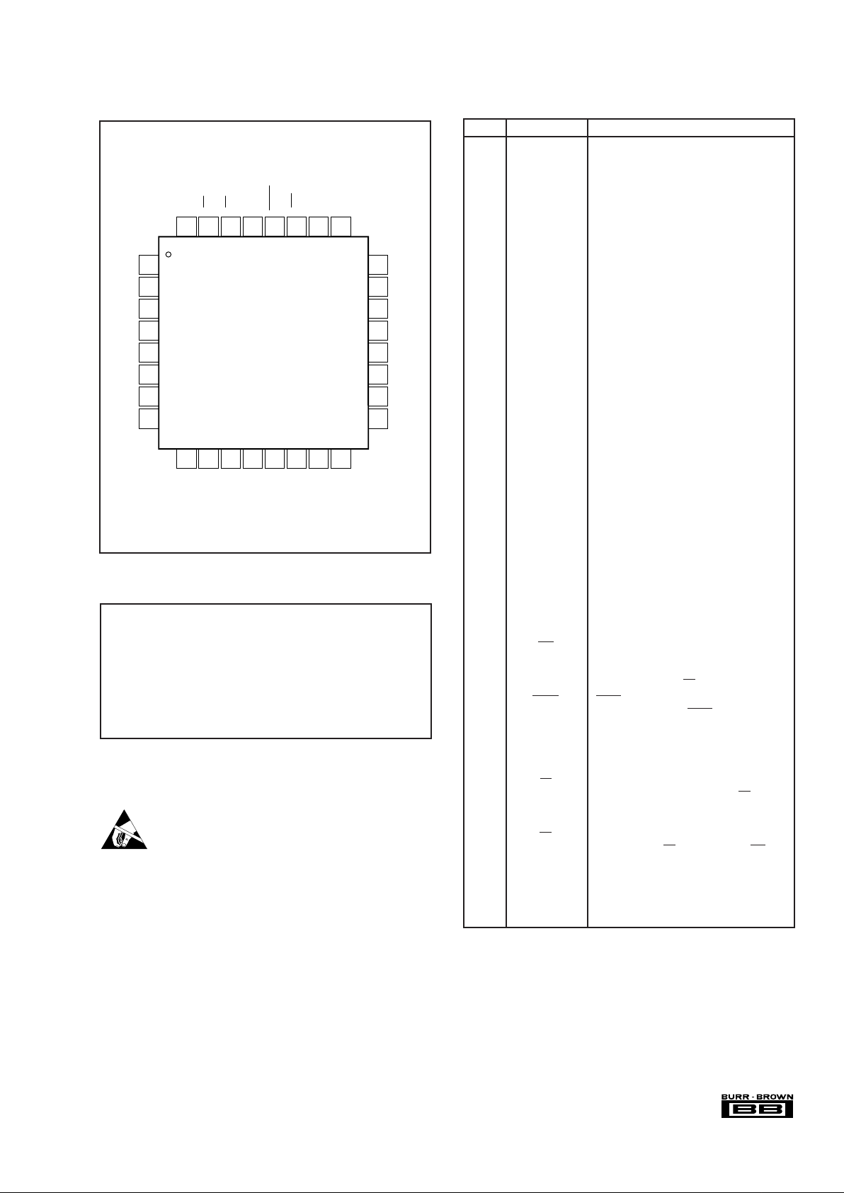
Top View TQFP
PIN NAME DESCRIPTION
1 AIN0 Analog Input Channel 0
2 AIN1 Analog Input Channel 1
3 AIN2 Analog Input Channel 2
4 AIN3 Analog Input Channel 3
5 AIN4 Analog Input Channel 4
6 AIN5 Analog Input Channel 5
7 AIN6 Analog Input Channel 6
8 AIN7 Analog Input Channel 7
9 AGND Analog Ground, GND = 0V
10 V
REF
Voltage Reference Input and Output. See
Specification Table for ranges. Decouple to
ground with a 0.1µF ceramic capacitor and
a 2.2µF tantalum capacitor.
11 DGND Digital Ground, GND = 0V
12 A2 Channel Address. See Channel Selection
Table for details.
13 A1 Channel Address. See Channel Selection
Table for details.
14 A0 Channel Address. See Channel Selection
Table for details.
15 DB11 Data Bit 11 (MSB)
16 DB10 Data Bit 10
17 DB9 Data Bit 9
18 DB8 Data Bit 8
19 DB7 Data Bit 7
20 DB6 Data Bit 6
21 DB5 Data Bit 5
22 DB4 Data Bit 4
23 DB3 Data Bit 3
24 DB2 Data Bit 2
25 DB1 Data Bit 1
26 DB0 Data Bit 0 (LSB)
27 WR Write Input. Active LOW. Use to start a
new conversion and to select an analog
channel via address inputs A0, A1 and A2
in combination with CS.
28 BUSY BUSY output goes LOW and stays LOW
during a conversion. BUSY rises when a
conversion is complete.
29 CLK
External Clock Input. The clock speed
determines the conversion rate by the
equation: f
CLK
= 16 • f
SAMPLE
.
30 RD Read Input. Active LOW. Use to read the
data outputs in combination with CS. Also
use (in conjunction with A0 or A1) to place
device in power-down mode.
31 CS Chip Select Input. Active LOW. The
combination of CS taken LOW and WR
taken LOW initiates a new conversion and
places the outputs in tri-state mode.
32 V
SS
Voltage Supply Input. Nominally +5V.
Decouple to ground with a 0.1µF ceramic
capacitor and a 10µF tantalum capacitor.
PIN ASSIGNMENTS
PIN CONFIGURATION
ELECTROSTATIC
DISCHARGE SENSITIVITY
Electrostatic discharge can cause damage ranging from performance degradation to complete device failure. BurrBrown Corporation recommends that all integrated circuits
be handled and stored using appropriate ESD protection
methods.
ESD damage can range from subtle performance degradation to complete device failure. Precision integrated circuits
may be more susceptible to damage because very small
parametric changes could cause the device not to meet
published specifications.
Analog Inputs to AGND, Any Channel Input ..............–0.3V to (VD + 0.3V)
REF
IN
.........................................................................–0.3V to (VD + 0.3V)
Digital Inputs to DGND ..............................................–0.3V to (V
D
+ 0.3V)
Ground Voltage Differences: AGND, DGND..................................... ±0.3V
+V
SS
to AGND..........................................................................–0.3V to 6V
Power Dissipation .......................................................................... 325mW
Maximum Junction Temperature ................................................... +150°C
Operating Temperature Range ......................................... –40°C to +85°C
Storage Temperature Range .......................................... –65°C to +150°C
Lead Temperature (soldering, 10s) ............................................... +300°C
NOTE: (1) Stresses above those listed under “Absolute Maximum Ratings” may
cause permanent damage to the device. Exposure to absolute maximum conditions for extended periods may affect device reliability.
ABSOLUTE MAXIMUM RATINGS
(1)
AIN0
AIN1
AIN2
AIN3
AIN4
AIN5
AIN6
AIN7
1
2
3
4
5
6
7
8
24
23
22
21
20
19
18
17
DB2
DB3
DB4
DB5
DB6
DB7
DB8
DB9
ADS7852Y
32
31
30
29
28
27
26
25
V
SS
CS
RD
CLK
BUSYWRDB0 (LSB)
DB1
9
10
11
12
13
14
15
16
AGND
V
REF
DGND
A2
A1
A0
DB11 (MSB)
DB10
Page 4

4
®
ADS7852
PACKAGE/ORDERING INFORMATION
MAXIMUM MAXIMUM
RELATIVE GAIN PACKAGE SPECIFICATION
ACCURACY ERROR DRAWING TEMPERATURE PACKAGE ORDERING TRANSPORT
PRODUCT (LSB) (LSB) PACKAGE NUMBER
(1)
RANGE MARKING
(2)
NUMBER
(3)
MEDIA
ADS7852Y ±2 ±25 TQFP-32 351 –40°C to +85°C A52 ADS7852Y/250 Tape and Reel
ADS7852Y
""""""ADS7852Y/2K5 Tape and Reel
ADS7852YB ±1 ±40 TQFP-32 351 –40°C to +85°C A52 ADS7852YB/250 Tape and Reel
ADS7852YB
""""""ADS7852YB/2K5 Tape and Reel
NOTE: (1) For detail drawing and dimension table, please see end of data sheet or Package Drawing File on Web. (2) Performance Grade information is marked
on the reel. (3) Models with a slash(/) are available only in Tape and reel in quantities indicated (e.g. /250 indicates 250 units per reel, /2K5 indicates 2500 devices
per reel). Ordering 2500 pieces of ”ADS7852Y/2K5“ will get a single 2500-piece Tape and Reel. For detailed Tape and Reel mechanical information, refer to the
www.burr-brown.com web site under Applications and Tape and Reel Orientation and Dimensions.
A2 A1 A0 CHANNEL SELECTED
0 0 0 Channel 0
0 0 1 Channel 1
0 1 0 Channel 2
0 1 1 Channel 3
1 0 0 Channel 4
1 0 1 Channel 5
1 1 0 Channel 6
1 1 1 Channel 7
ADS7852 CHANNEL SELECTION
Page 5

5
®
ADS7852
TYPICAL PERFORMANCE CURVES
At TA = +25°C, VSS = +5V, f
SAMPLE
= 500kHz, f
CLK
= 16 • f
SAMPLE
, and internal reference, unless otherwise specified.
SPECTRAL PERFORMANCE
(4096 Point FFT, f
IN
= 49.561kHz, –0.5dB)
Frequency (kHz)
0 50 100 150 200 250
Amplitude (dB)
0
–20
–40
–60
–80
–100
–120
SPECTRAL PERFORMANCE
(4096 Point FFT, f
IN
= 100.7081kHz, –0.5dB)
Frequency (kHz)
0 50 100 150 200 250
Amplitude (dB)
0
–20
–40
–60
–80
–100
–120
SPECTRAL PERFORMANCE
(4096 Point FFT, f
IN
= 199.5851kHz, –0.5dB)
Frequency (kHz)
0 50 100 150 200 250
Amplitude (dB)
0
–20
–40
–60
–80
–100
–120
SPECTRAL PERFORMANCE
(4096 Point FFT, f
IN
= 247.1921kHz, –0.5dB)
Frequency (kHz)
0 50 100 150 200 250
Amplitude (dB)
0
–20
–40
–60
–80
–100
–120
CHANGE IN SPURIOUS FREE DYNAMIC RANGE AND
TOTAL HARMONIC DISTORTION vs TEMPERATURE
Temperature (°C)
–50 –25 0 25 50 75 100
SFDR Delta from +25°C (dB)
THD Delta from +25°C (dB)
1.0
0.5
0.0
–0.5
–1.0
–1.0
–0.5
0.0
0.5
1.0
SFDR
THD
*
*
First nine harmonics
of the input frequency
fIN = 49.6kHz,–0.5dB
CHANGE IN SIGNAL-TO-NOISE RATIO AND
SIGNAL-TO-(NOISE+DISTORTION) vs TEMPERATURE
Temperature (°C)
–50 –25 0 25 50 75 100
SNR and SINAD Delta from +25°C (dB)
0.4
0.3
0.2
0.1
0.0
–0.1
–0.2
–0.3
–0.4
–0.5
SINAD
SNR
fIN = 49.6kHz,–0.5dB
Page 6

6
®
ADS7852
TYPICAL PERFORMANCE CURVES (Cont.)
At TA = +25°C, VSS = +5V, f
SAMPLE
= 500kHz, f
CLK
= 16 • f
SAMPLE
, and internal reference, unless otherwise specified.
SIGNAL-TO-NOISE and
SIGNAL-TO-(NOISE+DISTORTION)
vs INPUT FREQUENCY
76
74
72
70
68
66
10k 100k 1M1k
Input Frequency (Hz)
SNR
SINAD
SNR and SINAD (dB)
SPURIOUS FREE DYNAMIC RANGE and
TOTAL HARMONIC DISTORTION
vs INPUT FREQUENCY
90
85
80
75
70
–90
–85
–80
–75
–70
10k 100k 1M1k
SFDR (dB)
THD (dB)
*First nine harmonics
of the input frequency
THD*
SFDR
INTEGRAL LINEARITY ERROR vs CODE
Output Code
000
H
400
H
800
H
C00
H
FFF
H
ILE (LSBs)
1.00
0.75
0.50
0.25
0.00
–0.25
–0.50
–0.75
–1.00
DIFFERENTIAL LINEARITY ERROR vs CODE
Output Code
000
H
400
H
800
H
C00
H
FFF
H
DLE (LSBs)
1.00
0.75
0.50
0.25
0.00
–0.25
–0.50
–0.75
–1.00
CHANGE IN INTERNAL REFERENCE VOLTAGE
vs TEMPERATURE
Temperature (°C)
–50 –25 0 25 50 75 100
Delta from +25°C (mV)
6.0
4.0
2.0
0.0
–2.0
–4.0
–6.0
CHANGE IN GAIN ERROR vs TEMPERATURE
Temperature (°C)
–50 –25 0 25 50 75 100
Delta from +25°C (LSB)
8
6
4
2
0
–2
–4
–6
–8
Page 7

7
®
ADS7852
TYPICAL PERFORMANCE CURVES (Cont.)
At TA = +25°C, VSS = +5V, f
SAMPLE
= 500kHz, f
CLK
= 16 • f
SAMPLE
, and internal reference, unless otherwise specified.
CHANGE IN GAIN ERROR vs TEMPERATURE
(With External 2.5V Reference)
Temperature (°C)
–50 –25 0 25 50 75 100
Delta from +25°C (LSB)
0.5
0.4
0.3
0.2
0.1
0
–0.1
–0.2
–0.3
–0.4
–0.5
CHANGE IN OFFSET vs TEMPERATURE
Temperature (°C)
–50 –25 0 25 50 75 100
Delta from +25°C (LSB)
1.0
0.8
0.6
0.4
0.2
0.0
–0.2
–0.4
CHANGE IN WORST-CASE CHANNEL-TO-CHANNEL
OFFSET MISMATCH vs TEMPERATURE
Temperature (°C)
–50 –25 0 25 50 75 100
Delta from +25°C (LSB)
0.10
0.05
0.00
–0.05
–0.10
CHANGE IN WORST-CASE CHANNEL-TO-CHANNEL
GAIN MISMATCH vs TEMPERATURE
Temperature (°C)
–50 –25 0 25 50 75 100
Delta from +25°C (LSB)
0.020
0.015
0.010
0.005
0.000
–0.005
–0.010
–0.015
–0.020
CHANGE IN WORST-CASE INTEGRAL LINEARITY
AND DIFFERENTIAL LINEARITY vs SAMPLE RATE
Sample Rate (kHz)
100 200 300 400 500 600 700 800
Delta Relative to f
SAMPLE
= 500kHz (LSB)
3.0
2.5
2.0
1.5
1.0
0.5
0.0
–0.5
–1.0
Delta IL
Delta DL
CHANGE IN WORST-CASE INTEGRAL LINEARITY
AND DIFFERENTIAL LINEARITY vs TEMPERATURE
Temperature (°C)
–50 –25 0 25 50 75 100
Delta from +25°C (LSB)
0.050
0.025
0.000
–0.025
–0.050
Delta DL
Delta IL
Page 8

8
®
ADS7852
TYPICAL PERFORMANCE CURVES (Cont.)
At TA = +25°C, VSS = +5V, f
SAMPLE
= 500kHz, f
CLK
= 16 • f
SAMPLE
, and internal reference, unless otherwise specified.
SUPPLY CURRENT vs TEMPERATURE
Temperature (°C)
–50 –25 0 25 50 75 100
Supply Current (mA)
2.680
2.675
2.670
2.665
2.660
2.655
f
SAMPLE
= 500kHz
SUPPLY CURRENT vs SAMPLE RATE
Sample Rate (kHz)
100 200 300 400 500 600
Supply Current (mA)
2.9
2.8
2.7
2.6
2.5
2.4
2.3
CHANGE IN NAP CURRENT AND SLEEP CURRENT
vs TEMPERATURE
Temperature (°C)
–50 –25 0 25 50 75 100
Delta from +25°C (µA)
25
20
15
10
5
0
–5
–10
Nap
Sleep
CHANGE IN GAIN AND OFFSET vs SUPPLY VOLTAGE
V
SS
(V)
4.75 4.80 4.85 4.90 4.95 5.00 5.05 5.10 5.20 5.255.15
Delta from V
SS
= 5.00V (LSB)
0.25
0.20
0.15
0.10
0.05
0.00
–0.05
–0.10
–0.15
–0.20
–0.25
Offset
Gain
30
25
20
15
10
5
0
POWER SUPPLY REJECTION
vs POWER SUPPLY RIPPLE FREQUENCY
Power Supply Rejection (mV/V)
100 10k 100k 1M1k10
Page 9

9
®
ADS7852
THEORY OF OPERATION
The ADS7852 is a high-speed successive approximation
register (SAR) analog-to-digital converter (A/D) with an
internal 2.5V bandgap reference. The architecture is based
on capacitive redistribution which inherently includes a
sample/hold function. The converter is fabricated on a 0.6micron CMOS process. See Figure 1 for the basic operating
circuit for the ADS7852.
The ADS7852 requires an external clock to run the conversion process. This clock can vary between 200kHz (12.5Hz
throughput) and 8MHz (500kHz throughput). The duty cycle
of the clock is unimportant as long as the minimum HIGH
and LOW times are at least 50ns and the clock period is at
least 125ns. The minimum clock frequency is governed by
the parasitic leakage of the Capacitive Digital-to-Analog
(CDAC) capacitors internal to the ADS7852.
The front-end input multiplexer of the ADS7852 features
eight single-ended analog inputs. Channel selection is performed using the address pins A0 (pin 14), A1 (pin 13), and
A2 (pin 12). When a conversion is initiated, the input
voltage is sampled on the internal capacitor array. While a
conversion is in progress, all channel inputs are disconnected from any internal function (see Truth Table for
addressing).
The range of the analog input is set by the voltage on the
V
REF
pin. With the internal 2.5V reference, the input range
is 0V to 5V. An external reference voltage can be placed on
V
REF
, overdriving the internal voltage. The range for the
external voltage is 2.0V to 2.55V, giving an input voltage
range of 4.0V to 5.1V.
FIGURE 1. Typical Circuit Configuration.
AIN0
AIN1
AIN2
AIN3
AIN4
AIN5
AIN6
AIN7
1
2
3
4
5
6
7
8
24
23
22
21
20
19
18
17
DB2
DB3
DB4
DB5
DB6
DB7
DB8
DB9
ADS7852Y
32
31
30
29
28
27
26
25
Chip Select
Read Input
Clock Input
Busy Output
Write Input
V
SS
CS
RD
CLK
BUSY
WR
DB0 (LSB)
DB1
9
10
11
12
13
14
15
16
A2 Select
A1 Select
A0 Select
AGND
V
REF
DGNDA2A1
A0
DB11 (MSB)
DB10
10µF
+
0.1µF
+5V
Analog Supply
+
2.2µF
+
0.1µF
+
0V to 5V
Page 10

10
®
ADS7852
ANALOG INPUTS
The ADS7852 features eight single-ended inputs. While the
static current into each analog input is basically zero, the
dynamic current depends on the input voltage and sample
rate. Essentially, the current into the device must charge the
internal hold capacitor during the sample period. After this
capacitor has been fully charged, no further input current is
required. For optimum performance, the source driving the
analog inputs must be capable of charging the input capacitance to a 12-bit settling level within the sample period. This
can be as little as 350ns in some operating modes. While the
converter is in the hold mode, or after the sampling capacitor
has been fully charged, the input impedance of the analog
input is greater than 1GΩ.
REFERENCE
The reference voltage on the V
REF
pin establishes the fullscale range of the analog input. The ADS7852 can operate
with a reference in the range of 2.0V to 2.55V corresponding
to a full-scale range of 4.0V to 5.1V.
The voltage at the V
REF
pin is internally buffered and this
buffer drives the capacitor DAC portion of the converter.
This is important because the buffer greatly reduces the
dynamic load placed on the reference source. Since the
voltage at V
REF
will be unavoidably affected by noise and
glitches generated during the conversion process, it is highly
recommended that the V
REF
pin be bypassed to ground as
outlined in the sections that follow.
INTERNAL REFERENCE
The ADS7852 contains an onboard 2.5V reference, resulting
in a 0V to 5V input range on the analog input. The Specifications Table gives the various specifications for the internal
reference. This reference can be used to supply a small
amount of source current to an external load but the load
should be static. Due to the internal 10kΩ resistor, a dynamic load will cause variations in the reference voltage,
and will dramatically affect the conversion result. Note that
even a static load will reduce the internal reference voltage
seen at the buffer input. The amount of reduction depends on
the load and the actual value of the internal “10kΩ” resistor.
The value of this resistor can vary by ±30%.
The V
REF
pin should be bypassed with a 0.1µF ceramic
capacitor placed as close to the ADS7852 as possible. In
addition, a 2.2µF tantalum capacitor should be used in
parallel with the ceramic capacitor.
EXTERNAL REFERENCE
The internal reference is connected to the V
REF
pin and to the
internal buffer via an on-chip 10kΩ series resistor. Because
of this configuration, the internal reference voltage can
easily be overridden by an external reference voltage. The
voltage range for the external voltage is 2.00V to 2.55V,
corresponding to an analog input range of 4.0V to 5.1V.
While the external reference will not have to provide significant dynamic current to the V
REF
in, it does have to drive the
series 10kΩ resistor that is connected to the 2.5V internal
reference. Accounting for the maximum difference between
the external reference voltage and the internal reference
voltage, and the processing variations for the on-chip 10kΩ
resistor, this current can be as high as 75µA. In addition, the
V
REF
pin should still be bypassed to ground with at least a
0.1µF ceramic capacitor placed as close to the ADS7852 as
possible. Depending on the particular reference and A/D
conversion speed, additional bypass capacitance may be
required, such as the 2.2µF tantalum capacitor shown in the
Typical Circuit Configuration (Figure 1). Close attention
should be paid to the stability of any external reference
source that is driving the large bypass capacitors present at
the V
REF
pin.
BASIC OPERATION
Figure 1 shows the simple circuit required to operate the
ADS7852 with Channel 0 selected. A conversion can be
initiated by bringing the WR pin (pin 27) LOW for a
minimum of 35ns. BUSY (pin 28) will output a LOW during
the conversion process and rises only after the conversion is
complete. The 12 bits of output data will be valid on pins 15
through 26 following the rising edge of BUSY.
STARTING A CONVERSION
A conversion is initiated on the falling edge of the WR
input, with valid signals on A0, A1, A2, and CS. The
ADS7852 will enter the conversion mode on the first rising
edge of the external clock following the WR pin going
LOW. The conversion process takes 13.5 clock cycles (1.5
cycles for the DB0 decision, 2 clock cycles for the DB5
decision, and 1 clock cycle for each of the other bit decisions). This allows 2.5 clock cycles for sampling. Upon
initiating a conversion, the BUSY output will go LOW
approximately 20ns after the falling edge of the WR pin.
The BUSY output will return HIGH just after the ADS7852
has finished a conversion and the output data will be valid
on pins 15 through 26. The rising edge of BUSY can be used
to latch the output data into an external device. It is recommended that the data be read immediately after each conversion since the switching noise of the asynchronous data
transfer can cause digital feedthrough degrading the
converter’s performance. See Figure 2.
CHANNEL ADDRESSING
The selection of the analog input channel to be converted is
controlled by address pins A0, A1, and A2. This channel
becomes active on the rising edge of WR with CS held LOW.
The data on the address pins should be stable for at least 10ns
prior to WR going HIGH.
The address pins are also used to control the power-down
functions of the ADS7852. Careful attention must be paid to
the status of the address pins following each conversion. If
the user does not want the ADS7852 to enter either of the
power-down modes following a conversion, the A0 and A1
pins must be LOW when RD and CS are returned HIGH after
reading the data at the end of a conversion (see the PowerDown Mode section of this data sheet for more details).
Page 11

11
®
ADS7852
READING DATA
Data from the ADS7852 will appear at pins 15 through 26.
The MSB will output on pin 15 while the LSB will output
on pin 26. The outputs are coded in Straight Binary (with
0V = 000H and 5V = FFFH). Following a conversion, the
BUSY pin will go HIGH. After BUSY has been HIGH for
at least t14 seconds, the CS and RD pins may be brought
LOW to enable the 12-bit output bus. CS and RD must be
held LOW for at least 25ns following BUSY HIGH. Data
will be valid 30ns after the falling edge of both CS and RD.
The output data will remain valid for 20ns following the
rising edge of both CS and RD. See Figure 2 for the read
cycle timing diagram.
FIGURE 2. ADS7852 Write/Read Timing.
DIGITAL OUTPUT
STRAIGHT BINARY
DESCRIPTION ANALOG INPUT BINARY CODE HEX CODE
Least Significant 1.2207mV
Bit (LSB)
Full Scale 4.99878V 1111 1111 1111 FFF
Midscale 2.5V 1000 0000 0000 800
Midscale –1LSB 2.49878V 0111 1111 1111 7FF
Zero Full Scale 0V 0000 0000 0000 000
Table I. Ideal Input Voltages and Output Codes.
SYMBOL DESCRIPTION MIN TYP MAX UNITS
t
CONV
Conversion Time 1.75 µs
t
ACQ
Acquisition Time 0.25 µs
t
CKP
Clock Period 125 5000 ns
t
CKL
Clock LOW 40 ns
t
CKH
Clock HIGH 40 ns
t
1
WR LOW Prior to Rising Edge of CLK
35 ns
t
2
WR LOW After Rising Edge of CLK 20 ns
t
3
CS LOW After Rising Edge of CLK 20 ns
t
4
CS and RD HIGH 25 ns
t
5
BUSY Delay After CS LOW 20 ns
t
6
RD LOW 25 ns
t
7
Address Hold Time 5 ns
t
8
Address Setup Time 5 ns
t
9
Bus Access Time 30 ns
t
10
Bus Relinquish Time 5 ns
t
11
CS to RD Setup Time 0 ns
t
12
RD to CS Hold Time 0 ns
t
13
CLK LOW to BUSY HIGH 10 ns
t
14
BUSY to RD Delay 0 ns
t
15
RD HIGH to CLK LOW 50 ns
123456789
10 11 12 13 14 15 16
123456789
10 11 12 13 14 15 16
12345678
CLK
HOLD
WR
CS
BUSY
RD
Address
Bus
Data
Bus
t
CKH
t
CKL
t
2
t
4
t
4
t
1
t
3
t
CONV
t
ACQ
t
CKP
Conversion n
Address n + 1 Address n + 2
Conversion n + 1
Hi-ZHi-Z Hi-Z
Data
Valid
Data
Valid
t
5
t
10
t
6
t
8
t
7
t
9
Page 12

12
®
ADS7852
FIGURE 3. Entering Nap Using RD and A0.
FIGURE 4. Initiating Wake-Up Using RD and A0.
POWER-DOWN MODE
The ADS7852 has two different power-down modes: the
Nap mode and the Sleep mode. In the Nap mode, all analog
and digital circuitry, with the exception of the voltage
reference, is powered off. In the Sleep mode, everything is
powered off.
While the Sleep mode affords the lowest power consumption, the time to come out of Sleep mode can be considerable
since it takes the internal reference voltage a finite amount of
time to power up and reach a stable value. This latency can
result in spurious output data for a minimum of ten conversion cycles at a 500kHz sampling rate. It should also be
noted that any external load connected to the V
REF
pin will
exacerbate this effect since a discharge path for the V
REF
bypass capacitor is provided during the Sleep cycle. Even the
parasitic leakage of the bypass capacitor itself should be
considered if the unit is left in the Sleep mode for an
extended period. After power-up, this capacitor must be
recharged by the internal reference voltage and the on-chip
10kΩ series resistor. Under worst-case conditions (e.g., the
bypass capacitor is completely discharged), the output data
can be invalid for several hundred milliseconds.
Since the Nap mode maintains the voltage on the V
REF
pin by
keeping the internal reference powered-up, valid conversions
are available immediately after the Nap mode is terminated.
The simplest way to use the power-down mode is following
a conversion. After a conversion has finished and BUSY has
returned HIGH, CS and RD must be brought LOW for a
minimum of 25ns. When RD and CS are returned HIGH, the
ADS7852 will enter the power-down mode on the rising
edge of RD. If CS is always kept LOW, the power-down
mode will be controlled exclusively by RD. Depending on
the status of the A0 and A1 address pins, the ADS7852 will
either enter the Nap mode, the Sleep mode, or be returned
to normal operation in the sampling mode. See Table II and
Figures 3 and 4 for further details.
RD A2 A1 A0 POWER-DOWN MODE
X 0 0 None
X 1 0 Sleep
X 0 1 Nap
X 1 1 Sleep
= Signifies rising edge of RD pin. X = Don't care
TABLE II. ADS7852 Power-Down Mode.
CS
RD
CLK
BUSY
A0
A1
t
11
t
12
t
7
t
8
t
6
NOTE: Rising edge of 1st RD while A0 = 1 initiates power-down immediately. A1 must be LOW to enter Nap mode.
t
13
t
14
CS
RD
CLK
A1
A0
t
11
t
12
t
7
t
8
t
6
t
15
NOTE: Rising edge of 2nd RD while A0 = 0 places the ADS7852 in sample mode. A1 must be LOW to initiate wake-up.
Page 13

13
®
ADS7852
In addition to using the address pins in conjunction with RD,
the power-down mode can also be terminated implicitly by
starting a new conversion (e.g., taking WR LOW while CS
is LOW). If it is desired to keep the ADS7852 in a powerdown state for a period that is greater than dictated by the
sampling rate, the convert signal driving the WR pin must be
disabled.
The typical supply current of the ADS7852, with a 5V
supply and a 500kHz sampling rate, is 2.6mA. In the Nap
mode, the typical supply current is 600µA. In the Sleep
mode, the current is typically reduced to 10µA.
LAYOUT
For optimum performance, care should be taken with the
physical layout of the ADS7852 circuitry. This is particularly true if the CLK input is approaching the maximum
throughput rate.
The basic SAR architecture is sensitive to glitches or sudden
changes on the power supply, reference, ground connections
and digital inputs that occur just prior to latching the output
of the analog comparator. Thus, driving any single conversion for an n-bit SAR converter, there are n “windows” in
which large external transient voltages can affect the conversion result. Such glitches might originate from switching
power supplies, nearby digital logic, or high power devices.
The degree of error in the digital output depends on the
reference voltage, layout, and the exact timing of the external event. Their error can change if the external event
changes in times with respect to the CLK input.
With this in mind, power to the ADS7852 should be clean
and well bypassed. A 0.1µF ceramic bypass capacitor should
be placed as close to the device as possible. In addition, a
1µF to 10µF capacitor is recommended. If needed an even
larger capacitor and a 5Ω or 10Ω series resistor may be used
to low pass filter a noisy supply. The ADS7852 draws very
little current from an external reference on average as the
reference voltage is internally buffered. However, glitches
from the conversion process appear at the V
REF
input and the
reference source must be able to handle this. Whether the
reference is internal or external, the V
REF
pin should be
bypassed with a 0.1µF capacitor. An additional larger capacitor may also be used, if desired. If the reference voltage
is external and originates from an op amp, make sure it can
drive the bypass capacitor or capacitors without oscillation.
The GND pin should be connected to a clean ground point. In
many cases, this will be the “analog” ground. Avoid connections which are too near the grounding point of a microcontroller
or digital signal processor. If needed, run a ground trace
directly from the converter to the power supply entry point.
The ideal layout will include an analog ground plane dedicated
to the converter and associated analog circuitry.
FIGURE 5. Timing Diagram and Test Circuits for Param-
eters in Figure 2.
Voltage Waveforms for t
dis
Load Circuit for t
dis
and t
en
D
OUT
Test Point
t
dis
Waveform 2, t
en
V
CC
t
dis
Waveform 1
100pF
C
LOAD
3kΩ
t
dis
CS/SHDN
D
OUT
Waveform 1
(1)
D
OUT
Waveform 2
(2)
90%
10%
V
IH
NOTES: (1) Waveform 1 is for an output with internal
conditions such that the output is HIGH unless disabled
by the output control. (2) Waveform 2 is for an output
with internal conditions such that the output is LOW
unless disabled by the output control.
 Loading...