

Page 1
ADS7845
FEATURES
● 5-WIRE TOUCH SCREEN INTERFACE
● RATIOMETRIC CONVERSION
● SINGLE SUPPLY: 2V to 5V
● UP TO 125kHz CONVERSION RATE
● SERIAL INTERFACE
● PROGRAMMABLE 8- OR 12-BIT RESOLUTION
● AUXILIARY ANALOG INPUTS
● FULL POWER-DOWN CONTROL
®
DESCRIPTION
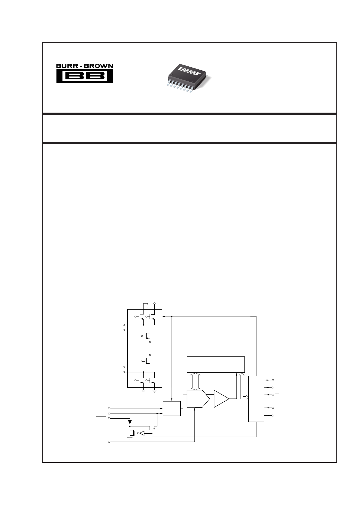
The ADS7845 is a 12-bit sampling analog-to-digital
converter (ADC) with a synchronous serial interface
and low on-resistance switches for driving touch
screens. Typical power dissipation is 750µW at a
125kHz throughput rate and a +2.7V supply. The
reference voltage (V
REF
) can be varied between 1V and
+VCC, providing a corresponding input voltage range
of 0V to V
REF
. The device includes a shutdown mode
which reduces typical power dissipation to under
0.5µW. The ADS7845 is guaranteed down to 2.7V
operation.
Low power, high speed, and on-board switches make
the ADS7845 ideal for battery-operated systems such
as personal digital assistants with resistive touch screens
and other portable equipment. The ADS7845 is available in a 16-lead SSOP package and is guaranteed
over the –40°C to +85°C temperature range.
APPLICATIONS
● PERSONAL DIGITAL ASSISTANTS
● PORTABLE INSTRUMENTS
● POINT-OF-SALES TERMINALS
● PAGERS
● TOUCH-SCREEN MONITORS
©
1998 Burr-Brown Corporation PDS-1497A Printed in U.S.A. December, 1998
TOUCH SCREEN CONTROLLER
CDAC
SAR
ADS7845
Comparator
MUX
Serial
Data
Interface
and
Control
DOUT
BUSY
CS
DCLK
DIN
UR
LR
UL
LL
AUX IN
WIPER
PENIRQ
V
REF
GND
Driver
+V
CC
+V
CC
GND
+V
CC
GND
International Airport Industrial Park • Mailing Address: PO Box 11400, Tucson, AZ 85734 • Street Address: 6730 S. Tucson Blvd., Tucson, AZ 85706 • Tel: (520) 746-1111
Twx: 910-952-1111 • Internet: http://www.burr-brown.com/ • Cable: BBRCORP • Telex: 066-6491 • FAX: (520) 889-1510 • Immediate Product Info: (800) 548-6132
ADS7845
Page 2
®
2
ADS7845
PARAMETER CONDITIONS MIN TYP MAX UNITS
RESOLUTION 12 Bits
ANALOG INPUT
Full-Scale Input Span Positive Input - Negative Input 0 V
REF
V
Absolute Input Range Positive Input –0.2 +V
CC
+0.2 V
Negative Input –0.2 +0.2 V
Capacitance 25 pF
Leakage Current 0.1 µA
SYSTEM PERFORMANCE
No Missing Codes 11 Bits
Integral Linearity Error ±2 LSB
(1)
Offset Error ±6 LSB
Gain Error ±4 LSB
Noise 30 µVrms
Power Supply Rejection Ratio 70 dB
SAMPLING DYNAMICS
Conversion Time 12 Clk Cycles
Acquisition Time 3 Clk Cycles
Throughput Rate 125 kHz
Multiplexer Settling Time 500 ns
Aperture Delay 30 ns
Aperture Jitter 100 ps
Channel-to-Channel Isolation V
IN
= 2.5Vp-p at 50kHz 100 dB
SWITCH DRIVERS
On-Resistance
UL, UR 7 Ω
LL, LR 7 Ω
REFERENCE INPUT
Range 1.0 +V
CC
V
Resistance CS = GND or +V
CC
5GΩ
Input Current 13 40 µA
f
SAMPLE
= 12.5kHz 2.5 µA
CS = +V
CC
0.001 3 µA
DIGITAL INPUT/OUTPUT
Logic Family CMOS
Logic Levels, Except PENIRQ
V
IH
| I
IH
| ≤ +5µA+V
CC
• 0.7 +VCC +0.3
V
IL
| I
IL
| ≤ +5µA –0.3 +0.8 V
V
OH
IOH = –250µA+V
CC
• 0.8 V
V
OL
IOL = 250µA 0.4 V
PENIRQ
V
OL
TA = 0°C to +85°C, 100kΩ Pull-Up 0.8 V
Data Format Straight Binary
POWER SUPPLY REQUIREMENTS
+V
CC
Specified Performance
(2)
2.7 5.5 V
Quiescent Current 280 650 µA
f
SAMPLE
= 12.5kHz 220 µA
Shutdown Mode with 3 µA
DCLK = DIN = +V
CC
Power Dissipation +VCC = +2.7V 1.8 mW
TEMPERATURE RANGE
Specified Performance –40 +85 °C
SPECIFICATIONS
At TA = –40°C to +85°C, +VCC = +2.7V, V
REF
= +2.5V, f
SAMPLE
= 125kHz, f
CLK
= 16 • f
SAMPLE
= 2MHz, 12-bit mode, and digital inputs = GND or +VCC, unless
otherwise noted.
The information provided herein is believed to be reliable; however, BURR-BROWN assumes no responsibility for inaccuracies or omissions. BURR-BROWN assumes
no responsibility for the use of this information, and all use of such information shall be entirely at the user’s own risk. Prices and specifications are subject to change
without notice. No patent rights or licenses to any of the circuits described herein are implied or granted to any third party. BURR-BROWN does not authorize or warrant
any BURR-BROWN product for use in life support devices and/or systems.
ADS7845E
NOTE: (1) LSB means Least Significant Bit. With V
REF
equal to +2.5V, one LSB is 610µV. (2) ADS7845 will operate down to 2.0V.
Page 3

®
3
ADS7845
PIN NAME DESCRIPTION
1+V
CC
Power Supply, 2.0V to 5V.
2 UL Upper Left Panel Driver (V
CC
ON/OFF)
3 UR Upper Right Panel Driver (switch between V
CC
and GND)
4 LL Lower Left Panel Driver (switch between GND
and V
CC
)
5 LR Lower Right Panel Driver (GND ON/OFF)
6 GND Ground
7 WIPER Panel Input
8 AUXIN Auxiliary Input
9V
REF
Voltage Reference Input
10 +V
CC
Power Supply, 2.0V to 5V.
11 PENIRQ Pen Interrupt. Open anode output (requires 10kΩ
to 100kΩ pull-up resistor externally).
12 DOUT Serial Data Output. Data is shifted on the falling
edge of DCLK. This output is high impedance
when CS is HIGH.
13 BUSY Busy Output. This output is high impedance when
CS is HIGH.
14 DIN Serial Data Input. If CS is LOW, data is latched on
rising edge of DCLK.
15 CS Chip Select Input. Controls conversion timing and
enables the serial input/output register.
16 DCLK External Clock Input. This clock runs the SAR con-
version process and synchronizes serial data I/O.
PIN CONFIGURATION
Top View SSOP
PIN DESCRIPTION
ABSOLUTE MAXIMUM RATINGS
(1)
+V
CC
to GND ........................................................................ –0.3V to +6V
Analog Inputs to GND ............................................ –0.3V to +V
CC
+ 0.3V
Digital Inputs to GND .............................................–0.3V to +V
CC
+ 0.3V
Power Dissipation .......................................................................... 250mW
Maximum Junction Temperature................................................... +150°C
Operating Temperature Range ........................................–40°C to +85°C
Storage Temperature Range ......................................... –65°C to +150°C
Lead Temperature (soldering, 10s) ............................................... +300°C
NOTE: (1) Stresses above those listed under “Absolute Maximum Ratings”
may cause permanent damage to the device. Exposure to absolute maximum
conditions for extended periods may affect device reliability.
ELECTROSTATIC
DISCHARGE SENSITIVITY
This integrated circuit can be damaged by ESD. Burr-Brown
recommends that all integrated circuits be handled with
appropriate precautions. Failure to observe proper handling and
installation procedures can cause damage.
ESD damage can range from subtle performance degradation to
complete device failure. Precision integrated circuits may be
more susceptible to damage because very small parametric
changes could cause the device not to meet its published specifications.
MAXIMUM
INTEGRAL PACKAGE SPECIFICATION
LINEARITY DRAWING TEMPERATURE ORDERING TRANSPORT
PRODUCT ERROR (LSB) PACKAGE NUMBER
(1)
RANGE NUMBER
(2)
MEDIA
ADS7845E ±2 16-Lead SSOP 322 –40°C to +85°C ADS7845E Rails
"" """ADS7845E/2K5 Tape and Reel
NOTES: (1) For detailed drawing and dimension table, please see end of data sheet, or Appendix C of Burr-Brown IC Data Book. (2) Models with a slash (/) are
available only in Tape and Reel in the quantities indicated (e.g., /2K5 indicates 2500 devices per reel). Ordering 2500 pieces of “ADS7845E/2K5” will get a single
2500-piece Tape and Reel. For detailed Tape and Reel mechanical information, refer to Appendix B of Burr-Brown IC Data Book.
PACKAGE/ORDERING INFORMATION
1
2
3
4
5
6
7
8
+V
CC
UL
UR
LL
LR
GND
WIPER
AUXIN
DCLK
CS
DIN
BUSY
DOUT
PENIRQ
+V
CC
V
REF
16
15
14
13
12
11
10
9
ADS7845
Page 4
®
4
ADS7845
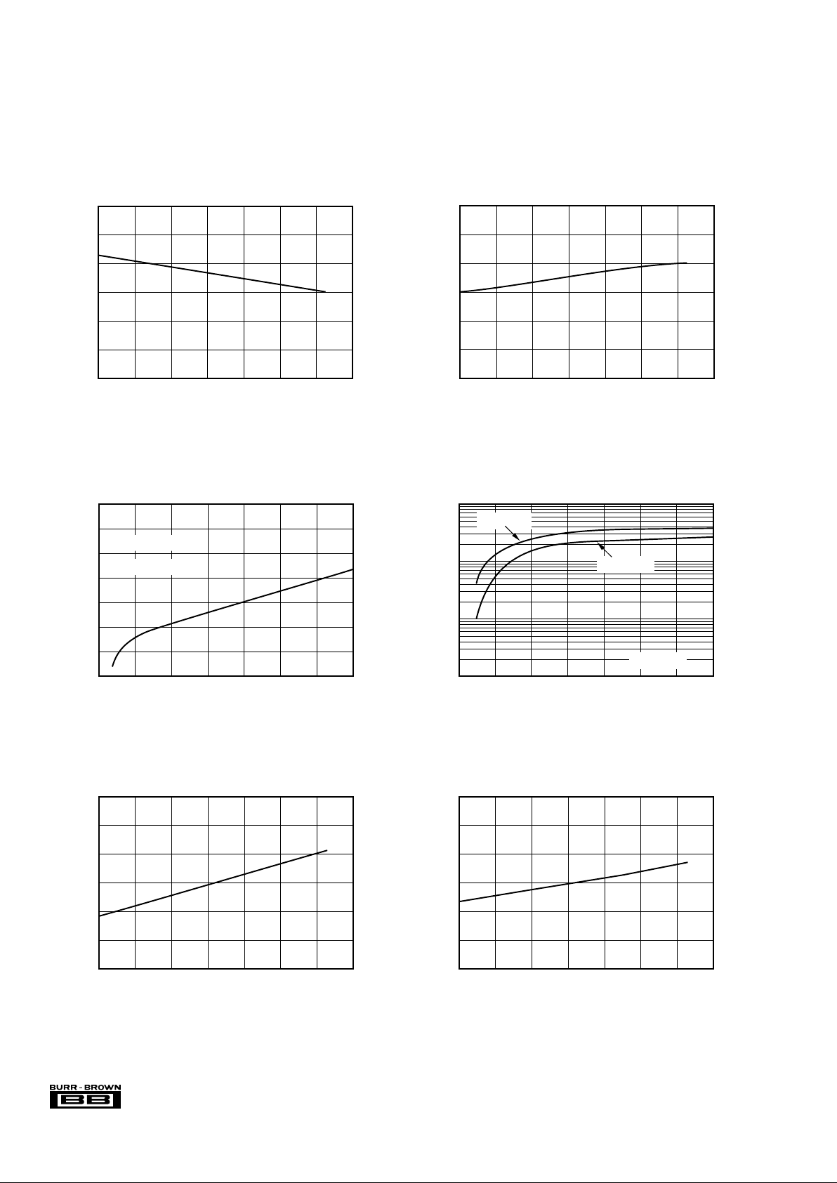
TYPICAL PERFORMANCE CURVES
At TA = +25°C, +VCC = +2.7V, V
REF
= +2.5V, f
SAMPLE
= 125kHz, and f
CLK
= 16 • f
SAMPLE
= 2MHz, unless otherwise noted.
SUPPLY CURRENT vs +V
CC
3.51.5 2 52.5 4
+V
CC
(V)
Supply Current (µA)
400
350
300
250
200
150
100
50
4.53
f
CLOCK
= 200kHz
V
REF
= +VCC
SUPPLY CURRENT vs TEMPERATURE
20–40 100–20 0 40
Temperature (°C)
Supply Current (µA)
400
350
300
250
200
150
100
60 80
POWER-DOWN SUPPLY CURRENT
vs TEMPERATURE
20–40 100–20 0 40
Temperature (°C)
Supply Current (nA)
140
120
100
80
60
40
20
60 80
MAXIMUM SAMPLE RATE vs +V
CC
3.51.5 2 52.5 4
+V
CC
(V)
Sample Rate (Hz)
1M
100k
10k
1k
4.53
V
REF
= +VCC
12-Bit Mode
8-Bit Mode
CHANGE IN GAIN vs TEMPERATURE
20–40 100–20 0 40
Temperature (°C)
Delta from +25°C (LSB)
0.15
0.10
0.05
0.00
–0.05
–0.10
–0.15
60 80
CHANGE IN OFFSET vs TEMPERATURE
20–40 100–20 0 40
Temperature (°C)
Delta from +25°C (LSB)
0.6
0.4
0.2
0.0
–0.2
–0.4
–0.6
60 80
Page 5

®
5
ADS7845
TYPICAL PERFORMANCE CURVES (CONT)
At TA = +25°C, +VCC = +2.7V, V
REF
= +2.5V, f
SAMPLE
= 125kHz, and f
CLK
= 16 • f
SAMPLE
= 2MHz, unless otherwise noted.
REFERENCE CURRENT vs SAMPLE RATE
750 12525 50 100
Sample Rate (kHz)
Reference Current (µA)
14
12
10
8
6
4
2
0
REFERENCE CURRENT vs TEMPERATURE
20–40 100–20 0 40
Temperature (°C)
Reference Current (µA)
18
16
14
12
10
8
6
60 80
2
1.8
1.6
1.4
1.2
1
0.8
0.6
0.4
0.2
0
LSB Error
20 40 60 80 100 120 140 160 180 200
Sampling Rate (kHz)
MAXIMUM SAMPLING RATE vs R
IN
INL: R = 2kΩ
INL: R = 500Ω
DNL: R = 2kΩ
DNL: R = 500Ω
SWITCH ON RESISTANCE vs TEMPERATURE
(X+, Y+: +V
CC
to Pin; X–, Y–: Pin to GND)
20–40 100–20
UL
LL
40
Temperature (°C)
R
ON
(Ω)
16
14
12
10
8
6
4
2
60 800
UR
LR
SWITCH ON RESISTANCE vs +V
CC
(X+, Y+: +VCC to Pin; X–, Y–: Pin to GND)
3.5252.5
UL
LL LR
4
+V
CC
(V)
R
ON
(Ω)
16
14
12
10
8
6
4
2
4.53
UR
Page 6

®
6
ADS7845
THEORY OF OPERATION
The ADS7845 is a classic Successive Approximation Register (SAR) analog-to-digital (A/D) converter. The architecture is based on capacitive redistribution which inherently
includes a sample/hold function. The converter is fabricated
on a 0.6µs CMOS process.
The basic operation of the ADS7845 is shown in Figure 1.
The device requires an external reference and an external
clock. It operates from a single supply of 2.0V to 5.25V. The
external reference can be any voltage between 1V and +VCC.
The value of the reference voltage directly sets the input
range of the converter. The average reference input current
depends on the conversion rate of the ADS7845.
The analog input to the converter is provided via the WIPER
input. In the measurement mode, the lower right corner of the
panel is connected to GND and the upper left corner is
connected to VCC. When the lower left corner is connected to
GND and the upper right corner is connected to VCC, a “Y”
measurement is made. When the lower left corner is connected to VCC and the upper right corner is connected
to GND, a “X” measurement is made. By maintaining a
differential input to the converter and a differential reference
architecture, it is possible to negate the switch’s on-resistance
error (should this be a source of error for the particular
measurement).
ANALOG INPUT
Figure 2 shows a block diagram of the input multiplexer on
the ADS7845, the differential input of the A/D converter, and
the converter’s differential reference. Table I and Table II
show the relationship between the A2, A1, A0, and SER/DFR
control bits and the configuration of the ADS7845. The
control bits are provided serially via the DIN pin—see the
Digital Interface section of this data sheet for more details.
When the converter enters the hold mode, the voltage difference between the +IN and –IN inputs (see Figure 2) is
captured on the internal capacitor array. The input current on
the analog inputs depends on the conversion rate of the
device. During the sample period, the source must charge the
internal sampling capacitor (typically 25pF). After the capacitor has been fully charged, there is no further input
current. The rate of charge transfer from the analog source to
the converter is a function of conversion rate.
A2 A1 A0 DRV1 DRV2 AUXIN
INTERRUPT
–IN
(1)
X POSITION Y POSITION +REF
(1)
–REF
(1)
0 0 1 ON GND OFF ON +V
REF
GND
1 0 1 ON GND ON OFF +V
REF
GND
0 1 0 ON GND OFF OFF +V
REF
GND
1 1 0 DOUT GND OFF OFF +V
REF
GND
TABLE I. Input Configuration—Single-Ended Reference Mode (SER/DFR HIGH).
NOTE: (1) Internal node, for clarification only—not directly accessible by the user.
A2 A1 A0 DRV1 DRV2 AUXIN
INTERRUPT
–IN
(1)
X SWITCHES Y SWITCHES +REF
(1)
–REF
(1)
0 0 1 ON LR OFF ON UL LR
1 0 1 ON LR ON OFF UL LR
0 1 0 ON GND OFF OFF +V
REF
GND
1 1 0 DOUT GND OFF OFF +V
REF
GND
NOTE: (1) Internal node, for clarification only—not directly accessible by the user.
TABLE II. Input Configuration—Differential Reference Mode (SER/DFR LOW).
FIGURE 1. Basic Operation of the ADS7845.
+V
CC
UL
UR
LL
LR
GND
WIPER
AUXIN
1
2
3
4
5
6
7
8
16
15
14
13
12
11
10
9
DCLK
CS
DIN
BUSY
DOUT
PENIRQ
+V
CC
V
REF
Serial/Conversion Clock
Chip Select
Serial Data In
Converter Status
Serial Data Out
+
1µF
to
10µF
(Optional)
+2.7V to +5V
ADS7845
Auxiliary Input
WIPER
0.1µF
Pen Interrupt
External reference required
with auxiliary input. Otherwise,
NC in differential mode or
V
CC
or external V
REF
in
single-ended mode.
100kΩ (optional)
0.1µF
Page 7

®
7
ADS7845
FIGURE 2. Simplified Diagram of ADS7845 Input and Panel Drivers.
REFERENCE INPUT
The voltage difference between +REF and –REF (see Figure
2) sets the analog input range. The ADS7845 will operate
with a reference in the range of 1V to +VCC. There are several
critical items concerning the reference input and its wide
voltage range. As the reference voltage is reduced, the analog
voltage weight of each digital output code is also reduced.
This is often referred to as the Least Significant Bit (LSB)
size and is equal to the reference voltage divided by 4096.
Any offset or gain error inherent in the A/D converter will
appear to increase, in terms of LSB size, as the reference
voltage is reduced. For example, if the offset of a given
converter is 2 LSBs with a 2.5V reference, it will typically be
5 LSBs with a 1V reference. In each case, the actual offset of
the device is the same, 1.22mV. With a lower reference
voltage, more care must be taken to provide a clean layout
including adequate bypassing, a clean (low noise, low ripple)
power supply, a low-noise reference, and a low-noise input
signal.
The voltage into the V
REF
input is not buffered and directly
drives the capacitor digital-to-analog converter (CDAC) portion of the ADS7845. Typically, the input current is 13µA
with V
REF
= 2.5V and f
SAMPLE
= 125kHz. This value will vary
by a few microamps depending on the result of the conversion. The reference current diminishes directly with both
conversion rate and reference voltage. As the current from the
reference is drawn on each bit decision, clocking the converter more quickly during a given conversion period will not
reduce overall current drain from the reference.
There is also a critical item regarding the reference when
making measurements where the switch drivers are on. For
this discussion, it’s useful to consider the basic operation of
the ADS7845 as shown in Figure 1. This particular application shows the device being used to digitize a resistive
touch screen. A measurement of the current Y position of
the pointing device is made with the WIPER input to the
A/D converter, turning on the UL and UR drivers to VCC,
grounding LL and LR, and digitizing the voltage on the
WIPER (see Figure 3 for a block diagram).
FIGURE 3. Simplified Diagram of Single-Ended Reference
(SER/DFR HIGH).
A/D CONVERTER
–REF
+REF Drivers
+IN
–IN
LL
LR
GND
SER/DFR
(Shown LOW)
UR
UL
+V
CC
PENIRQ V
REF
WIPER
AUXIN
A/D Converter
+V
CC
GND
V
REF HI
WIPER
UR
LR
UL
LL
V
REF LO
GND
GND
GND+V
CC
IN
LOW
Page 8

®
8
ADS7845
Under the situation outlined so far, it would not be possible
to achieve a zero volt input or a full-scale input regardless of
where the pointing device is on the touch screen because
some voltage is lost across the internal switches. In addition,
the internal switch resistance is unlikely to track the resistance of the touch screen, providing an additional source of
error.
This situation can be remedied as shown in Figure 4. By
setting the SER/DFR bit LOW, the +REF and –REF inputs
are connected directly to Y+ and Y–. This makes the analogto-digital conversion ratiometric. The result of the conversion is always a percentage of the external resistance, regardless of how it changes in relation to the on-resistance of
the internal switches. NOTE: There is an important consideration regarding power dissipation when using the
ratiometric mode of operation. See the Power Dissipation
section for more details.
processor and the converter consists of 8 clock cycles. One
complete conversion can be accomplished with three serial
communications, for a total of 24 clock cycles on the DCLK
input.
The first 8 clock cycles are used to provide the control byte
via the DIN pin. When the converter has enough information
about the following conversion to set the input multiplexer,
switches, and reference inputs appropriately, the converter
enters the acquisition (sample) mode and, if needed, the
internal switches are turned on. After three more clock
cycles, the control byte is complete and the converter enters
the conversion mode. At this point, the input sample/hold
goes into the hold mode and the internal switches may
turn off. The next 12 clock cycles accomplish the actual
analog-to-digital conversion. If the conversion is ratiometric
(SER/DFR LOW), the internal switches are on during the
conversion. A 13th clock cycle is needed for the last bit of
the conversion result. Three more clock cycles are needed to
complete the last byte (DOUT will be LOW). These will be
ignored by the converter.
Control Byte
Also shown in Figure 5 is the placement and order of the
control bits within the control byte. Tables III and IV give
detailed information about these bits. The first bit, the ‘S’ bit,
must always be HIGH and indicates the start of the control
byte. The ADS7845 will ignore inputs on the DIN pin until
the start bit is detected. The next three bits (A2 - A0) select
the active panel drivers (see Tables I and II and Figure 2).
The MODE bit determines the number of bits for each
conversion, either 12 bits (LOW) or 8 bits (HIGH).
The SER/DFR bit controls the reference mode: either singleended (HIGH) or differential (LOW). (The differential mode
is also referred to as the ratiometric conversion mode.) In
FIGURE 4. Simplified Diagram of Differential Reference
(SER/DFR LOW).
As a final note about the differential reference mode, it must
be used with +VCC as the source of the +REF voltage and
cannot be used with V
REF
. It is possible to use a high
precision reference on V
REF
and single-ended reference
mode for measurements which do not need to be ratiometric.
Or, in some cases, it could be possible to power the converter directly from a precision reference. Most references
can provide enough power for the ADS7845, but they might
not be able to supply enough current for the external load
(such as a resistive touch screen).
DIGITAL INTERFACE
Figure 5 shows the typical operation of the ADS7845’s digital
interface. This diagram assumes that the source of the digital
signals is a microcontroller or digital signal processor with
a basic serial interface. Each communication between the
BIT NAME DESCRIPTION
7 S Start Bit. Control byte starts with first HIGH bit on
DIN. A new control byte can start every 15th clock
cycle in 12-bit conversion mode or every 11th clock
cycle in 8-bit conversion mode.
6 - 4 A2 - A0 Channel Select Bits. Along with the SER/DFR bit,
these bits control the setting of the multiplexer input,
switches, and reference inputs, as detailed in Tables
I and II.
3 MODE 12-Bit/8-Bit Conversion Select Bit. This bit controls
the number of bits for the following conversion: 12
bits (LOW) or 8 bits (HIGH).
2 SER/DFR Single-Ended/Differential Reference Select Bit. Along
with bits A2 - A0, this bit controls the setting of the
multiplexer input, switches, and reference inputs, as
detailed in Tables I and II.
1 - 0 PD1 - PD0 Power-Down Mode Select Bits. See Table V for
details.
TABLE IV.Descriptions of the Control Bits within the
Control Byte.
BIT 7 BIT 6 BIT 5 BIT 4 BIT 3 BIT 2 BIT 1 BIT 0
(MSB) (LSB)
S A2 A1 A0 MODE
SER/DFR
PD1 PD0
TABLE III. Order of the Control Bits in the Control Byte.
A/D Converter
+V
CC
GND
V
REF HI
WIPER
UR
LR
UL
LL
V
REF LO
IN
LO
GND
+V
CC
GND
GND+V
CC
Page 9

®
9
ADS7845
single-ended mode, the converter’s reference voltage is
always the difference between the V
REF
and GND pins. In
differential mode, the reference voltage is the difference
between the currently enabled switches. See Tables I and II
and Figures 2 through 4 for more information. The last two
bits (PD1 - PD0) select the power- down mode as shown in
Table V. If both inputs are HIGH, the device is always
powered up. If both inputs are LOW, the device enters a
power-down mode between conversions. When a new conversion is initiated, the device will resume normal operation
instantly—no delay is needed to allow the device to power
up and the very first conversion will be valid. There are two
power-down modes: one where PENIRQ is disabled and
one where it is enabled.
PD1 PD0 PENIRQ DESCRIPTION
0 0 Enabled Power-down between conversions. When each
conversion is finished, the converter enters a
LOW power mode. At the start of the next conversion, the device instantly powers up to full
power. There is no need for additional delays to
assure full operation and the very first conversion
is valid. The LR– switch is on while in power-down.
0 1 Disabled Same as mode 00, except PENIRQ is disabled.
The LR– switch is off while in power-down mode.
1 0 Disabled Reserved for future use.
1 1 Disabled No power down between conversions, device is
always powered.
FIGURE 5. Conversion Timing, 24 Clocks per Conversion, 8-Bit Bus Interface. No DCLK Delay Required with Dedicated
Serial Port.
TABLE V. Power-Down Selection.
FIGURE 6. Conversion Timing, 16 Clocks per Conversion, 8-Bit Bus Interface. No DCLK Delay Required with Dedicated
Serial Port.
1
DCLK
CS
81
11
DOUT
BUSY
S
DIN
CONTROL BITS
S
CONTROL BITS
1098765 43210
11 10 9
81 18
t
ACQ
AcquireIdle Conversion Idle
1
DCLK
CS
81
11
DOUT
BUSY
DRIVERS 1 AND 2
(1)
(SER/DFR HIGH)
DRIVERS 1 AND 2
(1, 2)
(SER/DFR LOW)
(MSB)
(START)
(LSB)
A2S
ON
ON
OFF OFF
OFF OFF
DIN
A1 A0
MODE
SER/
DFR
PD1 PD0
1098765 4 3210 Zero Filled...
81 8
NOTES: (1) For Y Position, Driver 1 is ON and Driver 2 is OFF. For X Position, Driver 1 is OFF and Driver 2 is ON. LR
will turn on when power-down mode is entered and PD1, PD0 = 00B. (2) Drivers will remain on if power-down mode is
11
B
(no power down) until selected input channel, reference mode, or power-down mode is changed, or CS is HIGH.
Page 10

®
10
ADS7845
16 Clocks per Conversion
The control bits for conversion n+1 can be overlapped with
conversion ‘n’ to allow for a conversion every 16 clock
cycles, as shown in Figure 6. This figure also shows possible
serial communication occurring with other serial peripherals
between each byte transfer between the processor and the
converter. This is possible provided that each conversion
completes within 1.6ms of starting. Otherwise, the signal
that has been captured on the input sample/hold may droop
enough to affect the conversion result. Note that the ADS7845
is fully powered while other serial communications are
taking place during a conversion.
Digital Timing
Figure 7 and Table VI provide detailed timing for the digital
interface of the ADS7845.
15 Clocks per Conversion
Figure 8 provides the fastest way to clock the ADS7845.
This method will not work with the serial interface of most
microcontrollers and digital signal processors as they are
generally not capable of providing 15 clock cycles per serial
transfer. However, this method could be used with Field
Programmable Gate Arrays (FPGAs) or Application Specific Integrated Circuits (ASICs). This effectively increases
the maximum conversion rate of the converter beyond the
values given in the Specification table, which assume 16
clock cycles per conversion.
SYMBOL DESCRIPTION MIN TYP MAX UNITS
t
ACQ
Acquisition Time 1.5 µs
t
DS
DIN Valid Prior to DCLK Rising 100 ns
t
DH
DIN Hold After DCLK HIGH 10 ns
t
DO
DCLK Falling to DOUT Valid 200 ns
t
DV
CS Falling to DOUT Enabled 200 ns
t
TR
CS Rising to DOUT Disabled 200 ns
t
CSS
CS Falling to First DCLK Rising 100 ns
t
CSH
CS Rising to DCLK Ignored 0 ns
t
CH
DCLK HIGH 200 ns
t
CL
DCLK LOW 200 ns
t
BD
DCLK Falling to BUSY Rising 200 ns
t
BDV
CS Falling to BUSY Enabled 200 ns
t
BTR
CS Rising to BUSY Disabled 200 ns
TABLE VI. Timing Specifications (+VCC = +2.7V and
Above, TA = –40°C to +85°C, C
LOAD
= 50pF).
FIGURE 7. Detailed Timing Diagram.
FIGURE 8. Maximum Conversion Rate, 15 Clocks per Conversion.
PD0
t
BDV
t
DH
t
CH
t
CL
t
DS
t
CSS
t
DV
t
BD
t
BD
t
TR
t
BTR
t
D0
t
CSH
DCLK
CS
11
DOUT
BUSY
DIN
10
1
DCLK
CS
11
DOUT
BUSY
A2S
DIN
A1 A0
MODE
SGL/
DIF
PD1 PD0
109876543210 111098765432
A1 A0
15 1 15 1
A2SA1A0
MODE
SGL/
DIF
PD1 PD0
A2S
Page 11

®
11
ADS7845
Data Format
The ADS7845 output data is in Straight Binary format as
shown in Figure 9. This figure shows the ideal output code
for the given input voltage and does not include the effects
of offset, gain, or noise.
FIGURE 9. Ideal Input Voltages and Output Codes.
8-Bit Conversion
The ADS7845 provides an 8-bit conversion mode that can
be used when faster throughput is needed and the digital
result is not as critical. By switching to the 8-bit mode, a
conversion is complete four clock cycles earlier. This could
be used in conjunction with serial interfaces that provide 12bit transfers or two conversions could be accomplished with
three 8-bit transfers. Not only does this shorten each conversion by four bits (25% faster throughput), but each conversion can actually occur at a faster clock rate. This is because
the internal settling time of the ADS7845 is not as critical—
settling to better than 8 bits is all that is needed. The clock
rate can be as much as 50% faster. The faster clock rate and
fewer clock cycles combine to provide a 2x increase in
conversion rate.
POWER DISSIPATION
There are two major power modes for the ADS7845: full power
(PD1 - PD0 = 11B) and auto power-down (PD1 - PD0 = 00B).
When operating at full speed and 16-clocks per conversion (as
shown in Figure 6), the ADS7845 spends most of its time
acquiring or converting. There is little time for auto powerdown, assuming that this mode is active. Therefore, the difference between full power mode and auto power-down is negligible. If the conversion rate is decreased by simply slowing the
frequency of the DCLK input, the two modes remain approximately equal. However, if the DCLK frequency is kept at the
maximum rate during a conversion but conversions are simply
done less often, the difference between the two modes is
dramatic.
Figure 10 shows the difference between reducing the DCLK
frequency (“scaling” DCLK to match the conversion rate) or
maintaining DCLK at the highest frequency and reducing
the number of conversions per second. In the later case, the
converter spends an increasing percentage of its time in
power-down mode (assuming the auto power-down mode is
active).
Another important consideration for power dissipation is the
reference mode of the converter. In the single-ended reference mode, the converter’s internal switches are on only
when the analog input voltage is being acquired (see Figure
5). Thus, the external device, such as a resistive touch
screen, is only powered during the acquisition period. In the
differential reference mode, the external device must be
powered throughout the acquisition and conversion periods
(see Figure 5). If the conversion rate is high, this could
substantially increase power dissipation.
LAYOUT
The following layout suggestions should provide the most
optimum performance from the ADS7845. However, many
portable applications have conflicting requirements concerning power, cost, size, and weight. In general, most
portable devices have fairly “clean” power and grounds
because most of the internal components are very low
power. This situation would mean less bypassing for the
converter’s power and less concern regarding grounding.
Still, each situation is unique and the following suggestions
should be reviewed carefully.
For optimum performance, care should be taken with the
physical layout of the ADS7845 circuitry. The basic SAR
architecture is sensitive to glitches or sudden changes on the
power supply, reference, ground connections, and digital
inputs that occur just prior to latching the output of the
analog comparator. Thus, during any single conversion for
an ‘n-bit’ SAR converter, there are n ‘windows’ in which
Output Code
0V
FS = Full-Scale Voltage = V
REF
(1)
1 LSB = V
REF
(1)
/4096
FS – 1 LSB
11...111
11...110
11...101
00...010
00...001
00...000
1 LSB
NOTES: (1) Reference voltage at converter: +REF–(–REF). See Figure 2.
(2) Input voltage at converter, after multiplexer: +IN–(–IN). See Figure 2
Input Voltage
(2)
(V)
FIGURE 10. Supply Current vs Directly Scaling the Fre-
quency of DCLK with Sample Rate or Keeping
DCLK at the Maximum Possible Frequency.
10k 100k1k 1M
f
SAMPLE
(Hz)
Supply Current (µA)
100
10
1
1000
f
CLK
= 2MHz
f
CLK
= 16 • f
SAMPLE
TA = 25°C
+V
CC
= +2.7V
Page 12

®
12
ADS7845
large external transient voltages can easily affect the conversion result. Such glitches might originate from switching
power supplies, nearby digital logic, and high power devices. The degree of error in the digital output depends on
the reference voltage, layout, and the exact timing of the
external event. The error can change if the external event
changes in time with respect to the DCLK input.
With this in mind, power to the ADS7845 should be clean
and well bypassed. A 0.1µF ceramic bypass capacitor should
be placed as close to the device as possible. A 1µF to 10µF
capacitor may also be needed if the impedance of the
connection between +VCC and the power supply is high.
The reference should be similarly bypassed with a 0.1µF
capacitor. If the reference voltage originates from an op
amp, make sure that it can drive the bypass capacitor without
oscillation. The ADS7845 draws very little current from the
reference on average, but it does place larger demands on the
reference circuitry over short periods of time (on each rising
edge of DCLK during a conversion).
The ADS7845 architecture offers no inherent rejection of
noise or voltage variation in regards to the reference input.
This is of particular concern when the reference input is tied
to the power supply. Any noise and ripple from the supply
will appear directly in the digital results. While high frequency noise can be filtered out, voltage variation due to line
frequency (50Hz or 60Hz) can be difficult to remove.
The GND pin should be connected to a clean ground point.
In many cases, this will be the “analog” ground. Avoid
connections which are too near the grounding point of a
microcontroller or digital signal processor. If needed, run a
ground trace directly from the converter to the power supply
entry or battery connection point. The ideal layout will
include an analog ground plane dedicated to the converter
and associated analog circuitry.
In the specific case of use with a resistive touch screen, care
should be taken with the connection between the converter
and the touch screen. Since resistive touch screens have
fairly low resistance, the interconnection should be as short
and robust as possible. Longer connections will be a source
of error, much like the on-resistance of the internal switches.
Likewise, loose connections can be a source of error when
the contact resistance changes with flexing or vibrations.
PENIRQ Output
The pen interrupt output function is detailed in Figure 11. By
connecting a pull-up resistor to VCC (typically 100kΩ), the
PENIRQ output is HIGH. While in the power-down mode,
with PD0 = PD1 = 0, the lower-right panel corner is
connected to GND and the PENIRQ output is connected to
the WIPER input. When the panel is touched, the PENIRQ
output goes LOW, due to the current path through the panel
to GND, initiating an interrupt to the processor. During the
measurement cycles for X and Y position, the PENIRQ
output diode will be internally connected to GND and the
WIPER disconnected from the PENIRQ diode to eliminate
any leakage current from the pull-up resistor to flow through
the WIPER, thus causing no errors.
In addition, when the DIN has selected A2 = 1, A1 = 1,
A0 = 0, and the ADS7845 is commanded into the powerdown mode (PD0 and PD1 = 0) and CS is LOW (when CS
is HI, the DOUT line is high impedance), the DOUT will be
LOW (all “0”s) during no touch and HI (all “1”s) when the
panel is touched. This feature eliminates the need for an
additional port to detect panel touch. Since all panels have
end resistance, all “0”s and all “1”s are an unused set of
codes.
FIGURE 11. PENIRQ Functional Block Diagram.
+V
CC
100kΩ
UR
OFFOFF
OFF
LR
ON
WIPER
UR, LL
Driver
PENIRQ
UL
LL
 Loading...