

Page 1
12-Bit
Pipelined
ADC
Error
Correction
Logic
Timing/Duty Cycle
Adjust (PLL)
Internal
Reference
3-State
Output
S/H
D11A
·
·
·
D0A
12-Bit
Pipelined
ADC
Error
Correction
Logic
3-State
Output
S/H
D11B
·
·
·
D0B
AV
DD
OE
A
V
DRV
SDATA SEN SCLK SEL
OVR
A
OVR
B
IN
A
CM
IN
A
INT/EXT
CLK
DV
A
DV
B
REFT
REFB
IN
B
V
IN
OE
B
STPD
IN
B
ADS5232
V
IN
Serial
Interface
DISABLE_PLL
Dual, 12-Bit, 65MSPS, +3.3V
Analog-to-Digital Converter
FEATURES DESCRIPTION
• Single +3.3V Supply
• High SNR: 70.7dBFS at fIN= 5MHz
• Total Power Dissipation:
Internal Reference: 371mW
External Reference: 335mW
• Internal or External Reference
• Low DNL: ±0.3LSB
• Flexible Input Range: 1.5V
• TQFP-64 Package
APPLICATIONS
• Communications IF Processing
• Communications Base Stations
• Test Equipment
• Medical Imaging
• Video Digitizing
• CCD Digitizing
to 2V
PP
ADS5232
SBAS294A – JUNE 2004 – REVISED MARCH 2006
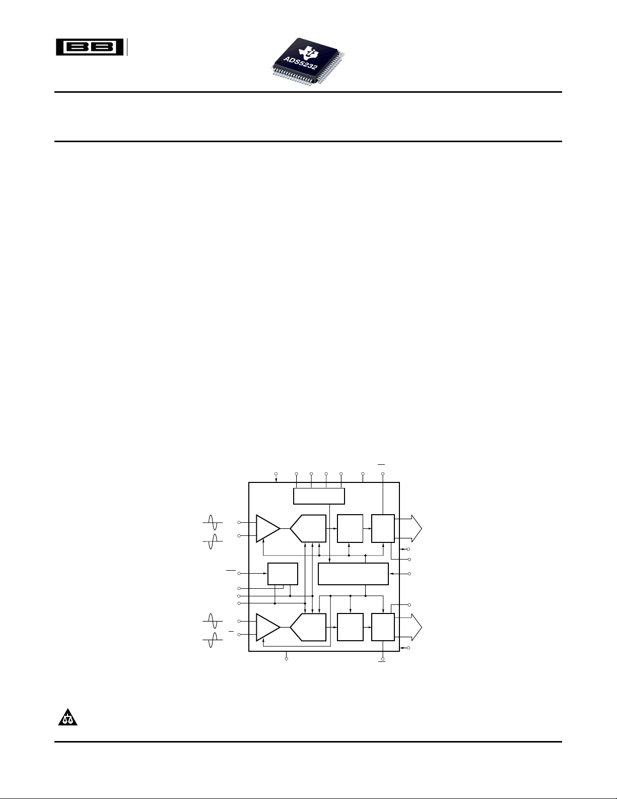
The ADS5232 is a dual, high-speed, high dynamic
range, 12-bit pipelined analog-to-digital converter
(ADC). This converter includes a high-bandwidth
sample-and-hold amplifier that gives excellent
spurious performance up to and beyond the Nyquist
rate. The differential nature of the sample-and-hold
amplifier and ADC circuitry minimizes even-order
harmonics and gives excellent common-mode noise
PP
immunity.
The ADS5232 provides for setting the full-scale range
of the converter without any external reference
circuitry. The internal reference can be disabled,
allowing low-drive, external references to be used for
improved tracking in multichannel systems.
The ADS5232 provides an over-range indicator flag
to indicate an input signal that exceeds the full-scale
input range of the converter. This flag can be used to
reduce the gain of front-end gain control circuitry.
There is also an output enable pin to allow for
multiplexing and testing on a PC board.
The ADS5232 employs digital error correction
techniques to provide excellent differential linearity for
demanding imaging applications. The ADS5232 is
available in a TQFP-64 package.
All trademarks are the property of their respective owners.
PRODUCTION DATA information is current as of publication date.
Products conform to specifications per the terms of the Texas
Instruments standard warranty. Production processing does not
necessarily include testing of all parameters.
Please be aware that an important notice concerning availability, standard warranty, and use in critical applications of Texas
Instruments semiconductor products and disclaimers thereto appears at the end of this data sheet.
Copyright © 2004–2006, Texas Instruments Incorporated
Page 2
www.ti.com
ADS5232
SBAS294A – JUNE 2004 – REVISED MARCH 2006
This integrated circuit can be damaged by ESD. Texas Instruments recommends that all integrated circuits be handled with
appropriate precautions. Failure to observe proper handling and installation procedures can cause damage.
ESD damage can range from subtle performance degradation to complete device failure. Precision integrated circuits may be more
susceptible to damage because very small parametric changes could cause the device not to meet its published specifications.
ORDERING INFORMATION
PRODUCT PACKAGE-LEAD DESIGNATOR RANGE MARKING NUMBER MEDIA, QUANTITY
ADS5232 TQFP-64 PAG –40°C to +85°C ADS5232IPAG
(1) For the most current package and ordering information see the Package Option Addendum at the end of this document, or see the TI
website at www.ti.com .
ABSOLUTE MAXIMUM RATINGS
PACKAGE TEMPERATURE PACKAGE ORDERING TRANSPORT
(1)
SPECIFIED
(1)
ADS5232IPAG Tray, 160
ADS5232IPAGT Tape and Reel, 250
over operating free-air temperature range (unless otherwise noted)
Supply Voltage Range, AVDD –0.3V to +3.8V
Supply Voltage Range, VDRV –0.3V to +3.8V
Voltage Between AVDD and VDRV –0.3V to +0.3V
Voltage Applied to External REF Pins –0.3V to +2.4V
Analog Input Pins
Case Temperature +100°C
Operating Free-Air Temperature Range, T
Lead Temperature +260°C
Junction Temperature +105°C
Storage Temperature –65°C +150°C
(1) Stresses above those listed under Absolute Maximum Ratings may cause permanent damage to the device. Exposure to absolute
maximum conditions for extended periods may affect device reliability.
(2) The DC voltage applied on the input pins should not go below –0.3V. Also, the DC voltage should be limited to the lower of either 3.3V
or (AVDD + 0.3V). If the input can go higher than +3.3V, then a resistor greater than or equal to 25 Ω should be added in series with
each of the input pins. Also, the duty cycle of the overshoot beyond +3.3V should be limited. The overshoot duty cycle can be defined
either as a percentage of the time of overshoot over a clock period, or over the entire device lifetime. For a peak voltage between +3.3V
and +3.5V, a duty cycle up to 10% is acceptable. For a peak voltage between +3.5V and +3.7V, the overshoot duty cycle should not
exceed 1%. Any overshoot beyond +3.7V should be restricted to less than 0.1% duty cycle, and never exceed +3.9V.
(2)
A
–0.3V to min [3.3V, (AVDD + 0.3V)]
–40°C to +85°C
2
Submit Documentation Feedback
Page 3

www.ti.com
SBAS294A – JUNE 2004 – REVISED MARCH 2006
RECOMMENDED OPERATING CONDITIONS
ADS5232
MIN TYP MAX UNITS
SUPPLIES AND REFERENCES
Analog Supply Voltage, AVDD 3.0 3.3 3.6 V
Output Driver Supply Voltage, VDRV 3.0 3.3 3.6 V
REF
— External Reference Mode 1.875 2.0 2.05 V
T
REF
— External Reference Mode 0.95 1.0 1.125 V
B
REFCM = (REF
Reference = (REF
Analog Input Common-Mode Range
+ REF
T
)/2 – External Reference Mode
B
– REF
T
) – External Reference Mode 0.75 1.0 1.1 V
B
(1)
CLOCK INPUT AND OUTPUTS
ADCLK Input Sample Rate
PLL Enabled (default) 20 65 MSPS
PLL Disabled 2 30
ADCLK Duty Cycle
PLL Enabled (default) 45 55 MSPS
Low-Level Voltage Clock Input 0.6 V
High-Level Voltage Clock Input 2.2 V
Operating Free-Air Temperature, T
A
Thermal Characteristics:
θ
JA
θ
JC
(1) These voltages need to be set to 1.5V ± 50mV if they are derived independent of VCM.
(2) When the PLL is disabled, the clock duty cycle needs to be controlled well, especially at higher speeds. A 45%–55% duty cycle variation
is acceptable up to a frequency of 30MSPS. If the device needs to be operated in the PLL disabled mode beyond 30MSPS, then the
duty cycle needs to be maintained within 48%–52% duty cycle.
(1)
V
± 50mV V
CM
V
± 50mV V
CM
(2)
–40 +85 °C
42.8 °C/W
18.7 °C/W
ADS5232
MSPS
Submit Documentation Feedback
3
Page 4

www.ti.com
ADS5232
SBAS294A – JUNE 2004 – REVISED MARCH 2006
ELECTRICAL CHARACTERISTICS
T
= –40°C and T
MIN
AVDD = 3.3V, VDRV = 3.3V, transformer-coupled inputs, –1dBFS, I
otherwise noted.
DC ACCURACY
No Missing Codes Tested
DNL Differential Nonlinearity fIN= 5MHz –0.9 ±0.3 +0.9 LSB
INL Integral Nonlinearity fIN= 5MHz –2.5 ±0.4 +2.5 LSB
Offset Error
Offset Temperature Coefficient
Fixed Attenuation in Channel
Fixed Attenuation Matching Across Channels 0.01 0.2 dB
Gain Error/Reference Error
Gain Error Temperature Coefficient ±40 ppm/°C
POWER REQUIREMENTS
Internal Reference
Power Dissipation
Total Power Dissipation 371 439 mW
External Reference
Power Dissipation Analog Only (AVDD) 224 mW
Total Power Dissipation 335 mW
VREF
T
VREF
B
Total Power-Down 88 mW
REFERENCE VOLTAGES
VREF
Reference Top (internal) 1.9 2.0 2.1 V
T
VREF
VREF
(1) Offset error is the deviation of the average code from mid-code with –1dBFS sinusoid from ideal mid-code (2048). Offset error is
(2) If the offset at temperatures T1and T2are O1and O2, respectively (where O1and O2are measured in LSBs), the offset temperature
(3) Fixed attenuation in the channel arises because of a fixed attenuation in the sample-and-hold amplifier. When the differential voltage at
(4) The reference voltages are trimmed at production so that (VREF
(5) Supply current can be calculated from dividing the power dissipation by the supply voltage of 3.3V.
(6) The V
(7) Average current drawn from the reference pins in the external reference mode.
Reference Bottom (internal) 0.9 1.0 1.1 V
B
V
Common-Mode Voltage 1.4 1.5 1.6 V
CM
V
Output Current
CM
VREF
Reference Top (external) 1.875 V
T
Reference Bottom (external) 1.125 V
B
External Reference Common-Mode V
External Reference Input Current
expressed in terms of % of full-scale.
coefficient in ppm/°C is calculated as (O
the analog input pins is changed from –V
(4096LSB) by the extent of this fixed attenuation. NOTE: V
does not include fixed attenuation.
output current specified is the drive of the V
CM
= +85°C. Typical values are at TA= +25°C, clock frequency = 65MSPS, 50% clock duty cycle,
MAX
= 56.2k Ω , and internal voltage reference, unless
SET
ADS5232
PARAMETER TEST CONDITIONS MIN TYP MAX UNITS
(1)
(2)
(3)
(4)
(5)
(5)
Analog Only (AVDD) 260 297 mW
–0.75 ±0.2 +0.75 %FS
±6 ppm/°C
1 %FS
–3.5 ±1.0 +3.5 % FS
Output Driver (VDRV) 111 142 mW
Output Driver (VDRV) 111 mW
1.875 2 2.05 mW
0.95 1 1.125 mW
(6)
(7)
– O2)/(T
1
to +V
REF
±50mV Change in Voltage ±2 mA
± 50mV V
CM
1.0 mA
– T2) × 1E6/4096.
1
, the swing of the output code is expected to deviate from the full-scale code
REF
CM
REF
buffer if loaded externally.
is defined as (REF
– VREF
T
– REF
T
) is within ± 35mV of the ideal value of 1V. This specification
B
).
B
4
Submit Documentation Feedback
Page 5
www.ti.com
SBAS294A – JUNE 2004 – REVISED MARCH 2006
ELECTRICAL CHARACTERISTICS (continued)
T
= –40°C and T
MIN
AVDD = 3.3V, VDRV = 3.3V, transformer-coupled inputs, –1dBFS, I
otherwise noted.
ANALOG INPUT
Differential Input Capacitance 3 pF
Analog Input Common-Mode Range V
Differential Input Voltage Range Internal Reference 2.02 V
Voltage Overload Recovery Time
Input Bandwidth 300 MHz
DIGITAL DATA INPUTS
Logic Family +3V CMOS Compatible
V
High-Level Input Voltage VIN= 3.3V 2.2 V
IH
V
Low-Level Input Voltage VIN= 3.3V 0.6 V
IL
C
Input Capacitance 3 pF
IN
DIGITAL OUTPUTS
Data Format Straight Offset Binary
Logic Family CMOS
Logic Coding Straight Offset Binary or BTC
Low Output Voltage (I
High Output Voltage (I
3-State Enable Time 2 Clocks
3-State Disable Time 2 Clocks
Output Capacitance 3 pF
SERIAL INTERFACE
SCLK Serial Clock Input Frequency 20 MHz
CONVERSION CHARACTERISTICS
Sample Rate 20 65 MSPS
Data Latency 6 CLK Cycles
(8) A differential ON/OFF pulse is applied to the ADC input. The differential amplitude of the pulse in its ON (high) state is twice the
full-scale range of the ADC, while the differential amplitude of the pulse in its OFF (low) state is zero. The overload recovery time of the
ADC is measured as the time required by the ADC output code to settle within 1% of full-scale, as measured from its mid-code value
when the pulse is switched from ON (high) to OFF (low).
(9) Option for Binary Two’s Complement Output.
= +85°C. Typical values are at TA= +25°C, clock frequency = 65MSPS, 50% clock duty cycle,
MAX
= 56.2k Ω , and internal voltage reference, unless
SET
ADS5232
PARAMETER TEST CONDITIONS MIN TYP MAX UNITS
± 0.05 V
CM
External Reference 2.02 × (VREF
(8)
– VREF
T
B
3 CLK Cycles
–3dBFS Input, 25 Ω Series
Resistance
(9)
= 50µA) +0.4 V
OL
= 50µA) +2.4 V
OH
) V
ADS5232
PP
PP
Submit Documentation Feedback
5
Page 6
www.ti.com
ADS5232
SBAS294A – JUNE 2004 – REVISED MARCH 2006
AC CHARACTERISTICS
T
= –40°C and T
MIN
cycle, AVDD = 3.3V, VDRV = 3.3V, –1dBFS, I
PARAMETER CONDITIONS MIN TYP MAX UNITS
DYNAMIC CHARACTERISTICS
SFDR Spurious-Free Dynamic Range fIN= 32.5MHz 85 dBc
HD
2nd-Order Harmonic Distortion fIN= 32.5MHz 87 dBc
2
HD
3rd-Order Harmonic Distortion fIN= 32.5MHz 85 dBc
3
SNR Signal-to-Noise Ratio fIN= 32.5MHz 69.5 dBFS
SINAD Signal-to-Noise and Distortion fIN= 32.5MHz 69 dBFS
Crosstalk –85 dBc
Two-Tone, Third-Order
IMD3 90.9 dBFS
Intermodulation Distortion
= +85°C. Typical values are at TA= +25°C, clock frequency = maximum specified, 50% clock duty
MAX
= 56.2k Ω , and internal voltage reference, unless otherwise noted.
SET
fIN= 5MHz 75 86 dBc
fIN= 70MHz 83 dBc
fIN= 5MHz 82 92 dBc
fIN= 70MHz 85 dBc
fIN= 5MHz 75 86 dBc
fIN= 70MHz 83 dBc
fIN= 5MHz 68 70.7 dBFS
fIN= 70MHz 67.5 dBFS
fIN= 5MHz 67.5 70.3 dBFS
fIN= 70MHz 67 dBFS
5MHz Full-Scale Signal Applied to 1 Channel;
Measurement Taken on the Channel with No Input Signal
f1= 4MHz at –7dBFS
f2= 5MHz at –7dBFS
ADS5242
6
Submit Documentation Feedback
Page 7
www.ti.com
Analog
Input
CLK
DATA[D11:D0]
DV
OE
DATA
D11:D0
t
OE
t
OE
t
DV
t
1
t
2
t
C
t
A
N + 1
N + 2 N+4
N + 3
N
ADS5232
SBAS294A – JUNE 2004 – REVISED MARCH 2006
TIMING DIAGRAM
TIMING CHARACTERISTICS
(1)
Typical values at TA= +25°C, AVDD = VDRV = 3.3V, sampling rate and PLL state are as indicated, input clock at 50% duty
cycle, and total capacitive loading = 10pF, unless otherwise noted.
PARAMETER MIN TYP MAX UNITS
tAAperture Delay 2.1 ns
Aperture Jitter 1.0 ps
tDR, tDFData Rise/Fall Time
t1Data Setup Time
t2Data Hold Time
tDData Latency 6 Clocks
Data Valid (DV) Duty Cycle 30 40 55 %
tDVInput Clock Rising to DV Fall Edge 10 11.5 14 ns
(1) Specifications assured by design and characterization; not production tested.
(2) Measured from data becoming valid (at a high level = 2.0V and a low level = 0.8V) to the 50% point of the falling edge of DV.
(3) Measured from the 50% point of the falling edge of DV to the data becoming invalid.
(4) Measured between 20% to 80% of logic levels.
(2)
(3)
(4)
65MSPS With PLL ON
2 3.2 ns
6.3 8.5 ns
0.5 2 3 ns
Submit Documentation Feedback
7
Page 8
www.ti.com
ADS5232
SBAS294A – JUNE 2004 – REVISED MARCH 2006
TIMING CHARACTERISTICS (continued)
Typical values at TA= +25°C, AVDD = VDRV = 3.3V, sampling rate and PLL state are as indicated, input clock at 50% duty
cycle, and total capacitive loading = 10pF, unless otherwise noted.
PARAMETER MIN TYP MAX UNITS
50MSPS With PLL ON
tAAperture Delay 2.1 ns
Aperture Jitter 1.0 ps
t1Data Setup Time 3.2 4.5 ns
t2Data Hold Time 10 11 ns
tDData Latency 6 Clocks
tDR, tDFData Rise/Fall Time 0.5 2 3 ns
Data Valid (DV) Duty Cycle 30 40 55 %
tDVInput Clock Rising to DV Fall Edge 11.5 13.5 15.5 ns
40MSPS With PLL ON
tAAperture Delay 2.1 ns
Aperture Jitter 1.0 ps
t1Data Setup Time 3.7 5.5 ns
t2Data Hold Time 11.5 13.5 ns
tDData Latency 6 Clocks
tDR, tDFData Rise/Fall Time 0.5 2 3 ns
Data Valid (DV) Duty Cycle 30 40 55 %
tDVInput Clock Rising to DV Fall Edge 13.5 16 18.5 ns
30MSPS With PLL OFF
tAAperture Delay 2.1 ns
Aperture Jitter 1.0 ps
t1Data Setup Time 8 10 ns
t2Data Hold Time 14 19 ns
tDData Latency 6 Clocks
tDR, tDFData Rise/Fall Time 0.5 2 3.5 ns
Data Valid (DV) Duty Cycle 30 45 55 %
tDVInput Clock Rising to DV Fall Edge 16 19 21 ns
20MSPS With PLL ON
tAAperture Delay 2.1 ns
Aperture Jitter 1.0 ps
t1Data Setup Time 10 12 ns
t2Data Hold Time 20 25 ns
tDData Latency 6 Clocks
tDR, tDFData Rise/Fall Time 0.5 2 3.5 ns
Data Valid (DV) Duty Cycle 30 45 55 %
tDVInput Clock Rising to DV Fall Edge 20 25 30 ns
20MSPS With PLL OFF
tAAperture Delay 2.1 ns
Aperture Jitter 1.0 ps
t1Data Setup Time 10 12 ns
t2Data Hold Time 20 25 ns
tDData Latency 6 Clocks
tDR, tDFData Rise/Fall Time 0.5 2 3.5 ns
Data Valid (DV) Duty Cycle 30 45 55 %
tDVInput Clock Rising to DV Fall Edge 20 25 30 ns
2MSPS With PLL OFF
tAAperture Delay 2.1 ns
Aperture Jitter 1.0 ps
t1Data Setup Time 150 200 ns
8
Submit Documentation Feedback
Page 9
www.ti.com
NOTE: Data is shifted in MSB first.
Start Sequence
t
1
t
7
t
6
D7
(MSB)
D6 D5 D4 D3 D2 D1 D0
t
2
t
3
t
4
t
5
CLK
SEN
SCLK
SDATA
Outputs change on
next rising clock edge
after SEN goes high.
Data latched on
each rising edge of SCLK.
SBAS294A – JUNE 2004 – REVISED MARCH 2006
TIMING CHARACTERISTICS (continued)
Typical values at TA= +25°C, AVDD = VDRV = 3.3V, sampling rate and PLL state are as indicated, input clock at 50% duty
cycle, and total capacitive loading = 10pF, unless otherwise noted.
PARAMETER MIN TYP MAX UNITS
t2Data Hold Time 200 250 ns
tDData Latency 6 Clocks
tDR, tDFData Rise/Fall Time 0.5 2 3.5 ns
Data Valid (DV) Duty Cycle 30 45 55 %
tDVInput Clock Rising to DV Fall Edge 200 225 250 ns
SERIAL INTERFACE TIMING
ADS5232
PARAMETER DESCRIPTION MIN TYP MAX UNIT
t
1
t
2
t
3
t
4
t
5
t
6
t
7
Serial CLK Period 50 ns
Serial CLK High Time 20 ns
Serial CLK Low Time 20 ns
Data Setup Time 5 ns
Data Hold Time 5 ns
SEN Fall to SCLK Rise 8 ns
SCLK Rise to SEN Rise 8 ns
Submit Documentation Feedback
9
Page 10

www.ti.com
ADS5232
SBAS294A – JUNE 2004 – REVISED MARCH 2006
SERIAL REGISTER MAP: Shown for the Case Where Serial Interface is Used
ADDRESS DATA DESCRIPTION
D7 D6 D5 D4 D3 D2 D1 D0
0 0 0 0 X X X 0 Normal Mode
0 0 0 0 X X X 1 Power-Down Both Channels
0 0 0 0 X X 0 X Straight Offset Binary Output
0 0 0 0 X X 1 X Binary Two's Complement Output
0 0 0 0 X 0 X X Channel B Digital Outputs Enabled
0 0 0 0 X 1 X X Channel B Digital Outputs Tri-Stated
0 0 0 0 0 X X X Channel A Digital Outputs Enabled
0 0 0 0 1 X X X Channel A Digital Outputs Tri-Stated
0 0 1 0 0 0 0 0 Normal Mode
0 0 1 0 0 1 0 0 All Digital Outputs Set to '1'
0 0 1 0 1 0 0 0 All Digital Outputs Set to '0'
0 0 1 1 0 0 X 0 Normal Mode
0 0 1 1 1 X X 0 Channel A Powered Down
0 0 1 1 X 1 X 0 Channel B Powered Down
(1)
0 0 1 1 X X 0 0 PLL Enabled (default)
0 0 1 1 X X 1 0 PLL Disabled
(1) X = don't care.
10
Submit Documentation Feedback
Page 11

www.ti.com
RECOMMENDED POWER-UP SEQUENCING
t
1
t
3
t
5
t
6
t
4
t
7
t
8
t
2
AVDD(3V to 3.6V)
VDRV (3V to 3.6V)
Device Ready
For ADC Operation
Device Ready
For ADC Operation
Device Ready
For Serial Register Write
Start of Clock
AVDD
VDRV
SEL
SEN
CLK
NOTE: 10µs < t
1
< 50ms; 10µs < t2< 50ms;−10ms < t3< 10ms; t4> 10ms; t5> 100ns; t6> 100ns; t7> 10ms; and t8> 100µs.
STPD
Device Fully
Powers Down
Device Fully
Powers Up
500µs
1µs
NOTE: The shown power−up time is based on 1µF bypass capacitors on the reference pins.
See the Theory of Operation section for details.
Shown for the case where the serial interface is used.
ADS5232
SBAS294A – JUNE 2004 – REVISED MARCH 2006
POWER-DOWN TIMING
Submit Documentation Feedback
11
Page 12

www.ti.com
Top View TQFP
48
47
46
45
44
43
42
41
40
39
38
37
36
35
34
33
AGND
AGND
AV
DD
STPD/SDATA
GND
VDRV
OEA/SCLK
MSBI/SEN
VDRV
OVR
A
D11_A (MSB)
D10_A
D9_A
D8_A
D7_A
D6_A
1
2
3
4
5
6
7
8
9
10
11
12
13
14
15
16
SEL
AGND
AV
DD
GND
VDRV
OE
B
GND
VDRV
OVR
B
D0_B (LSB)
D1_B
D2_B
D3_B
D4_B
D5_B
D6_B
AGND
IN
B+
IN
B−
AGND
I
SET
AGND
AGND
AV
DD
INT/EXT
AGND
REFB
REFT
CM
IN
A
−
IN
A+
AGND
D7_B
D8_B
D9_B
D10_B
D11_B (MSB)
DV
B
GND
CLK
GND
DV
A
D0_A (LSB)
D1_A
D2_A
D3_A
D4_A
D5_A
64 63 62 61 60 59 58 57 56 55 54
17 18 19 20 21 22 23 24 25 26 27
53 52 51 50 49
28 29 30 31 32
ADS5232
ADS5232
SBAS294A – JUNE 2004 – REVISED MARCH 2006
PIN CONFIGURATION
NAME PIN # I/O DESCRIPTION
AGND 2, 47–49, 55, 58, 59, 61, 64 Analog Ground
AVDD 3, 46, 57 Analog Supply
CLK 24 I Clock Input
CM 52 O Common-Mode Voltage Output
D0_A (LSB) 27 O Data Bit 12 (D0), Channel A
D1_A 28 O Data Bit 11 (D1), Channel A
D2_A 29 O Data Bit 10 (D2), Channel A
D3_A 30 O Data Bit 9 (D3), Channel A
D11_A (MSB) 38 O Data Bit 1 (D11), Channel A
D0_B (LSB) 10 O Data Bit 12 (D0), Channel B
12
D4_A 31 O Data Bit 8 (D4), Channel A
D5_A 32 O Data Bit 7 (D5), Channel A
D6_A 33 O Data Bit 6 (D6), Channel A
D7_A 34 O Data Bit 5 (D7), Channel A
D8_A 35 O Data Bit 4 (D8), Channel A
D9_A 36 O Data Bit 3 (D9), Channel A
D10_A 37 O Data Bit 2 (D10), Channel A
Submit Documentation Feedback
PIN DESCRIPTIONS
Page 13

www.ti.com
PIN DESCRIPTIONS (continued)
NAME PIN # I/O DESCRIPTION
D1_B 11 O Data Bit 11 (D1), Channel B
D2_B 12 O Data Bit 10 (D2), Channel B
D3_B 13 O Data Bit 9 (D3), Channel B
D4_B 14 O Data Bit 8 (D4), Channel B
D5_B 15 O Data Bit 7 (D5), Channel B
D6_B 16 O Data Bit 6 (D6), Channel B
D7_B 17 O Data Bit 5 (D7), Channel B
D8_B 18 O Data Bit 4 (D8), Channel B
D9_B 19 O Data Bit 3 (D9), Channel B
D10_B 20 O Data Bit 2 (D10), Channel B
D11_B (MSB) 21 O Data Bit 1 (D11), Channel B
DV
A
DV
B
GND 4, 7, 23, 25, 44 Output Buffer Ground
IN
A
IN
A
IN
B
IN
B
INT/ EXT 56 I
I
SET
MSBI/SEN 41 I 1 = Binary Two's Complement, 0 = Straight Offset Binary (Default)
OE
/SCLK 42 I 0 = Enabled (Default), 1 = Tri-State
A
OE
B
OVR
A
OVR
B
REF
B
REF
T
SEL 1 I
STPD/SDATA 45 I 0 = Normal Operation (Default), 1 = Enabled
VDRV 5, 8, 40, 43 Output Buffer Supply
26 O Data Valid, Channel A
22 O Data Valid, Channel B
50 I Analog Input, Channel A
51 I Complementary Analog Input, Channel A
63 I Analog Input, Channel B
62 I Complementary Analog Input, Channel B
Reference Select; 0 = External (Default), 1 = Internal; Force high to set for internal reference
operation.
60 O Bias Current Setting Resistor of 56.2k Ω to Ground
When SEL = 0, MSBI (Most Significant Bit Invert)
When SEL = 1, SEN (Serial Write Enable)
When SEL = 0, OE
(Output Enable Channel A)
A
When SEL = 1, SCLK (Serial Write Clock)
6 I Output Enable, Channel B (0 = Enabled [Default], 1 = Tri-State)
39 O Over-Range Indicator, Channel A
9 O Over-Range Indicator, Channel B
54 I/O Bottom Reference/Bypass (2 Ω resistor in series with a 0.1 µ F capacitor to ground)
53 I/O Top Reference/Bypass (2 Ω resistor in series with a 0.1 µ F capacitor to ground)
Serial interface select signal. Setting SEL = 0 configures pins 41, 42, and 45 as MSBI, OE
STPD, respectively. With SEL = 0, the serial interface is disabled. Setting SEL = 1 enables the serial
interface and configures pins 41, 42, and 45 as SEN, SCLK, and SDATA, respectively. Serial
registers can be programmed using these three signals. When used in this mode of operation, it is
essential to provide a low-going pulse on SEL in order to reset the serial interface registers as soon
as the device is powered up. SEL therefore also has the functionality of a RESET signal.
When SEL = 0, STPD (Power Down)
When SEL = 1, SDATA (Serial Write Data)
ADS5232
SBAS294A – JUNE 2004 – REVISED MARCH 2006
, and
A
Submit Documentation Feedback
13
Page 14

www.ti.com
SINAD 10Log
10
P
S
PN P
D
SNR 10Log
10
P
S
P
N
ENOB
SINAD 1.76
6.02
ADS5232
SBAS294A – JUNE 2004 – REVISED MARCH 2006
DEFINITION OF SPECIFICATIONS
Analog Bandwidth
The analog input frequency at which the spectral
power of the fundamental frequency (as determined
by FFT analysis) is reduced by 3dB.
Aperture Delay
The delay in time between the rising edge of the input
sampling clock and the actual time at which the
sampling occurs.
Aperture Uncertainty (Jitter)
The sample-to-sample variation in aperture delay.
Clock Duty Cycle
Pulse width high is the minimum amount of time that
the ADCLK pulse should be left in logic ‘1’ state to
achieve rated performance. Pulse width low is the
minimum time that the ADCLK pulse should be left in
a low state (logic ‘0’). At a given clock rate, these
specifications define an acceptable clock duty cycle.
Minimum Conversion Rate
This is the minimum sampling rate where the ADC
still works.
Signal-to-Noise and Distortion (SINAD)
SINAD is the ratio of the power of the fundamental
(P
) to the power of all the other spectral components
S
including noise (P
) and distortion (P
N
), but not
D
including DC.
SINAD is either given in units of dBc (dB to carrier)
when the absolute power of the fundamental is used
as the reference, or dBFS (dB to full-scale) when the
power of the fundamental is extrapolated to the
full-scale range of the converter.
Signal-to-Noise Ratio (SNR)
SNR is the ratio of the power of the fundamental (P
to the noise floor power (P
DC and the first eight harmonics.
), excluding the power at
N
)
S
Differential Nonlinearity (DNL)
An ideal ADC exhibits code transitions that are
exactly 1 LSB apart. DNL is the deviation of any
single LSB transition at the digital output from an
ideal 1 LSB step at the analog input. If a device
claims to have no missing codes, it means that all
possible codes (for a 12-bit converter, 4096 codes)
are present over the full operating range.
Effective Number of Bits (ENOB)
The ENOB is a measure of converter performance as
compared to the theoretical limit based on
quantization noise.
Integral Nonlinearity (INL)
INL is the deviation of the transfer function from a
reference line measured in fractions of 1 LSB using a
best straight line or best fit determined by a least
square curve fit. INL is independent from effects of
offset, gain or quantization errors.
Maximum Conversion Rate
The encode rate at which parametric testing is
performed. This is the maximum sampling rate where
certified operation is given.
SNR is either given in units of dBc (dB to carrier)
when the absolute power of the fundamental is used
as the reference, or dBFS (dB to full-scale) when the
power of the fundamental is extrapolated to the
full-scale range of the converter.
Spurious-Free Dynamic Range
The ratio of the power of the fundamental to the
highest other spectral component (either spur or
harmonic). SFDR is typically given in units of dBc (dB
to carrier).
Two-Tone, Third-Order Intermodulation Distortion
Two-tone IMD3 is the ratio of power of the
fundamental (at frequencies f1and f2) to the power of
the worst spectral component of third-order
intermodulation distortion at either frequency 2f
or 2f
– f1. IMD3 is either given in units of dBc (dB to
2
carrier) when the absolute power of the fundamental
is used as the reference, or dBFS (dB to full-scale)
when the power of the fundamental is extrapolated to
the full-scale range of the converter.
– f
1
2
14
Submit Documentation Feedback
Page 15

www.ti.com
TYPICAL CHARACTERISTICS
Amplitude (dBFS)
Input Frequency (MHz)
0
−
20
−
40
−
60
−
80
−
100
−
120
0
19.5 266.5 13 32.5
fIN= 1MHz
SNR = 71.4dBFS
SINAD = 71.3dBFS
SFDR = 87.5dBc
Amplitude (dBFS)
Input Frequency (MHz)
0
−
20
−
40
−
60
−
80
−
100
−
120
0
19.5 266.5 13 32.5
fIN= 5MHz
SNR = 71.4dBFS
SINAD = 71.3dBFS
SFDR = 84.5dBc
Amplitude (dBFS)
Input Frequency (MHz)
0
−
20
−
40
−
60
−
80
−
100
−
120
0
19.5 266.5 13 32.5
fIN= 32.5MHz
SNR =70.6dBFS
SINAD = 70.4dBFS
SFDR = 88.6dBc
Amplitude (dBFS)
Input Frequency (MHz)
0
−
20
−
40
−
60
−
80
−
100
−
120
0
19.5 266.5 13 32.5
fIN= 70MHz
SNR = 67.7dBFS
SINAD = 67.6dBFS
SFDR = 83.9dBc
DNL (LSB)
Code
0.4
0.3
0.2
0.1
0
−
0.1
−
0.2
−
0.3
−
0.4
0
2048 30721024 4096
f
IN
= 5MHz
Amplitude (dBFS)
Input Frequency (MHz)
0
−
20
−
40
−
60
−
80
−
100
−
120
0
19.5 266.5 13 32.5
f1= 4MHz (−7dBFS)
f2= 5MHz (−7dBFS)
IMD =−97.9dBFS
T
= –40°C and T
MIN
AVDD = 3.3V, VDRV = 3.3V, transformer-coupled inputs, –1dBFS, I
= +85°C. Typical values are at TA= +25°C, clock frequency = 65MSPS, 50% clock duty cycle,
MAX
otherwise noted.
SPECTRAL PERFORMANCE SPECTRAL PERFORMANCE
Figure 1. Figure 2.
SBAS294A – JUNE 2004 – REVISED MARCH 2006
= 56.2k Ω , and internal voltage reference, unless
SET
ADS5232
SPECTRAL PERFORMANCE SPECTRAL PERFORMANCE
Figure 3. Figure 4.
INTERMODULATION DISTORTION DIFFERENTIAL NONLINEARITY
Figure 5. Figure 6.
Submit Documentation Feedback
15
Page 16

www.ti.com
INL (LSB)
Code
1.0
0.8
0.6
0.4
0.2
0
−
0.2
−
0.4
−
0.6
−
0.8
−
1.0
0
2048 30721024 4096
fIN= 5MHz
IAVDD, IDVDD (mA)
Sample Rate (MHz)
0.10
0.09
0.08
0.07
0.06
0.05
0.04
0.03
0.02
0.01
0
20 25 30 35 40 45 50 55 60 65
70
fIN= 5MHz
IAVDD
IVDRV
SNR (dBFS), SFDR (dBc)
Input Frequency (MHz)
110
100
90
80
70
60
50
40
30
0 20
8040 60 100
SNR
SFDR
SNR, SINAD (dBFS), SFDR (dBc)
Clock Frequency (MHz)
95
90
85
80
75
70
65
60
55
20 25 30 35 40 45 50 55 60 65 70
SNR
SFDR
SINAD
fIN= 5MHz
SNR (dBFS), SFDR (dBc)
Input Frequency (MHz)
110
100
90
80
70
60
50
40
30
0
40 60 8020 100
SNR
SFDR
External Reference:
REF = 2V
T
REF = 1V
B
SNR (dBFS), SFDR (dBc)
Duty Cycle (%)
95
90
85
80
75
70
65
60
30 35 50 55 60 6540 45 70
fIN= 5MHz
SNR
SFDR
ADS5232
SBAS294A – JUNE 2004 – REVISED MARCH 2006
TYPICAL CHARACTERISTICS (continued)
T
= –40°C and T
MIN
AVDD = 3.3V, VDRV = 3.3V, transformer-coupled inputs, –1dBFS, I
otherwise noted.
= +85°C. Typical values are at TA= +25°C, clock frequency = 65MSPS, 50% clock duty cycle,
MAX
INTEGRAL NONLINEARITY IAVDD, IVDRV vs CLOCK FREQUENCY
Figure 7. Figure 8.
= 56.2k Ω , and internal voltage reference, unless
SET
DYNAMIC PERFORMANCE vs CLOCK FREQUENCY DYNAMIC PERFORMANCE vs INPUT FREQUENCY
Figure 9. Figure 10.
DYNAMIC PERFORMANCE vs CLOCK DUTY CYCLE
DYNAMIC PERFORMANCE vs INPUT FREQUENCY WITH PLL ENABLED (default)
16
Figure 11. Figure 12.
Submit Documentation Feedback
Page 17

www.ti.com
SNR (dBFS), SFDR (dBc)
Temperature (C)
95
90
85
80
75
70
65
60
55
−
40
−
15 +60+10 +35 +85
fIN= 5MHz
SNR
SFDR
Power Dissipation (mW)
Temperature (C)
405
390
375
360
345
330
−
40
+10 +35 +60
−
15 +85
fIN= 5MHz
SNR, SFDR (dBc), SNR (dBFS)
Input Amplitude (dBFS)
100
90
80
70
60
50
40
30
20
10
0
−
70−60
−
30−20−10
−
50−40 0
fIN= 5MHz
SNR (dBFS)
SNR (dBc)
SFDR (dBc)
Samples
Code
4000
3500
3000
2500
2000
1500
1000
500
0
N
−
5
N
−
4
N
−
3
N
−
2
N
−
1
N
N + 1
N + 2
N + 3
N + 4
N + 5
SNR, SFDR (dBc), SNR (dBFS)
Input Amplitude (dBFS)
100
90
80
70
60
50
40
30
20
10
0
−
70−60
−
30−20−10
−
50−40 0
fIN= 32.5MHz
SNR (dBFS)
SNR (dBc)
SFDR (dBc)
TYPICAL CHARACTERISTICS (continued)
T
= –40°C and T
MIN
AVDD = 3.3V, VDRV = 3.3V, transformer-coupled inputs, –1dBFS, I
otherwise noted.
= +85°C. Typical values are at TA= +25°C, clock frequency = 65MSPS, 50% clock duty cycle,
MAX
SBAS294A – JUNE 2004 – REVISED MARCH 2006
= 56.2k Ω , and internal voltage reference, unless
SET
ADS5232
DYNAMIC PERFORMANCE vs TEMPERATURE
POWER DISSIPATION vs TEMPERATURE
Figure 13. Figure 14.
OUTPUT NOISE SWEPT INPUT POWER
Figure 15. Figure 16.
SWEPT INPUT POWER
Figure 17.
Submit Documentation Feedback
17
Page 18

www.ti.com
ADS5232
SBAS294A – JUNE 2004 – REVISED MARCH 2006
APPLICATION INFORMATION
THEORY OF OPERATION INPUT CONFIGURATION
The ADS5232 is a dual-channel, simultaneous The analog input for the ADS5232 consists of a
sampling analog-to-digital converter (ADC). Its low differential sample-and-hold architecture implemented
power and high sampling rate of 65MSPS is achieved using a switched capacitor technique; see Figure 18 .
using a state-of-the-art switched capacitor pipeline The sampling circuit consists of a low-pass RC filter
architecture built on an advanced low-voltage CMOS at the input to filter out noise components that
process. The ADS5232 operates from a +3.3V supply potentially could be differentially coupled on the input
voltage for both its analog and digital supply pins. The inputs are sampled on two 4pF capacitors.
connections. The ADC core of each channel consists The RLC model is illustrated in Figure 18 .
of a combination of multi-bit and single-bit internal
pipeline stages. Each stage feeds its data into the
digital error correction logic, ensuring excellent
differential linearity and no missing codes at the
12-bit level. The conversion process is initiated by the
rising edge of the external clock. Once the signal is
captured by the input sample-and-hold amplifier, the
input sample is sequentially converted within the
pipeline stages. This process results in a data latency
of six clock cycles, after which the output data is
available as a 12-bit parallel word, coded in either
straight offset binary (SOB) or binary two's
complement (BTC) format. Since a common clock
controls the timing of both channels, the analog
signal is sampled simultaneously. The data on the
parallel ports is updated simultaneously as well.
Further processing can be timed using the individual
data valid output signal of each channel. The
ADS5232 features internal references that are
trimmed to ensure a high level of accuracy and
matching. The internal references can be disabled to
allow for external reference operation.
INPUT DRIVER CONFIGURATIONS
Transformer-Coupled Interface
If the application requires a signal conversion from a
single-ended source to drive the ADS5232
differentially, an RF transformer could be a good
solution. The selected transformer must have a
center tap in order to apply the common-mode DC
voltage (V
AC grounding the center tap will generate the
differential signal swing across the secondary
winding. Consider a step-up transformer to take
advantage of signal amplification without the
introduction of another noise source. Furthermore,
the reduced signal swing from the source may lead to
improved distortion performance. The differential
input configuration may provide a noticeable
advantage for achieving good SFDR performance
over a wide range of input frequencies. In this mode,
both inputs (IN and IN) of the ADS5232 see matched
impedances.
Figure 19 illustrates the schematic for the suggested
transformer-coupled interface circuit. The component
values of the RC low-pass filter may be optimized
depending on the desired roll-off frequency.
) necessary to bias the converter inputs.
CM
18
Submit Documentation Feedback
Page 19

www.ti.com
5nH
to 9nH
3.2pF
to 4.8pF
IN OUT
IN
P
1.5pF to
2.5pF
1
Ω
15
Ω
to 25
Ω
5nH
to 9nH
IN
N
1.5pF to
2.5pF
1
Ω
15
Ω
to 25
Ω
60
Ω
to 120
Ω
1.5pF
to 1.9pF
IN OUT
3.2pF
to 4.8pF
IN OUT
15
Ω
to 25
Ω
15
Ω
to 25
Ω
60
Ω
to 120
Ω
IN OUT
IN
OUT
15Ωto 35
Ω
IN OUT
IN OUT
OUT
P
OUT
N
Switches that are ON
in SAMPLE phase.
Switches that are ON
in HOLD phase.
V
IN
IN
IN
CM
+1.5V
24.9
Ω
24.9
Ω
0.1µF
22pF
R
T
1:n
0.1µF
R
G
R
2
R
1
OPA690
49.9
Ω
1/2
ADS5232
One Channel of Two
ADS5232
SBAS294A – JUNE 2004 – REVISED MARCH 2006
Figure 18. Input Circuitry
Figure 19. Converting a Single-Ended Input Signal into a Differential Signal Using an RF-Transformer
Submit Documentation Feedback
19
Page 20

www.ti.com
1µF
C
F
C
F
1/2
ADS5232
THS4503
R
ISO
R
ISO
R
S
V
S
R
G
R
T
R
F
R
F
V
OCM
10µF 0.1µF
0.1µF
IN
IN
CM
R
G
AVDD
+5V
REF
T
CM REF
B
I
SET
INT/EXTADS5232
0.1µF 2.2µF
+ +
2
Ω
2
Ω
56k
Ω
AVDD
2.2µF 0.1µF
ADS5232
SBAS294A – JUNE 2004 – REVISED MARCH 2006
DC-Coupled Input with Differential Amplifier
Applications that have a requirement for DC-coupling
a differential amplifier, such as the THS4503, can be
used to drive the ADS5232; this design is shown in
Figure 20 . The THS4503 amplifier easily allows a
single-ended to differential conversion, which reduces
component cost.
REFERENCE CIRCUIT
Internal Reference
All bias currents required for the proper operation of
the ADS5232 are set using an external resistor at I
(pin 60), as shown in Figure 21 . Using a 56.2k Ω
resistor on I
generates an internal reference
SET
SET
current of about 20 µ A. This current is mirrored
internally to generate the bias current for the internal
blocks. While a 5% resistor tolerance is adequate,
deviating from this resistor value alters and degrades
device performance. For example, using a larger
external resistor at I
reduces the reference bias
SET
current and thereby scales down the device operating
power.
Figure 20. Using the THS4503 with the ADS5232
In addition, the V
pin on the THS4503 can be
OCM
directly tied to the common-mode pin (CM) of the
ADS5232 to set up the necessary bias voltage for the
converter inputs. In the circuit example shown in
Figure 20 , the THS4503 is configured for unity gain. If
required, a higher gain can easily be achieved as well
by adding small capacitors (such as 10pF) in parallel
with the feedback resistors to create a low-pass filter.
Since the THS4503 is driving a capacitive load, small
series resistors in the output ensure stable operation.
Figure 21. Internal Reference Circuit
Further details of this and the overall operation of the
THS4503 may be found in its product data sheet
(available for download at www.ti.com ). In general,
differential amplifiers provide a high-performance
driver solution for baseband applications, and other
differential amplifier models may be selected
depending on the system requirements.
As part of the internal reference circuit, the ADS5232
provides a common-mode voltage output at pin 52,
CM. This common-mode voltage is typically +1.5V.
While this is similar to the common-mode voltage
used internally within the ADC pipeline core, the
CM-pin has an independent buffer amplifier, which
can deliver up to ±2mA of current to an external
Input Over-Voltage Recovery
The differential full-scale input range supported by the
ADS5232 is 2V
. For a nominal value of V
PP
CM
(+1.5V), IN and IN can swing from 1V to 2V. The
ADS5232 is especially designed to handle an
over-voltage differential peak-to-peak voltage of 4V
(2.5V and 0.5V swings on IN and IN). If the input
common-mode voltage is not considerably different
from V
recovery from an over-voltage input condition is
expected to be within three clock cycles. All of the
amplifiers in the sample-and-hold stage and the ADC
core are especially designed for excellent recovery
from an overload signal.
20
during overload (less than 300mV),
CM
Submit Documentation Feedback
circuit for proper input signal level shifting and
biasing. In order to obtain optimum dynamic
performance, the analog inputs should be biased to
the recommended common-mode voltage (1.5V).
While good performance can be maintained over a
certain CM-range, larger deviations may compromise
device performance and could also negatively affect
the overload recovery behavior. Using the internal
reference mode requires the INT/ EXT pin to be
forced high, as shown in Figure 21 .
The ADS5232 requires solid high-frequency
bypassing on both reference pins, REF
and REF
T
see Figure 21 . Use ceramic 0.1 µ F capacitors (size
0603, or smaller), located as close as possible to the
pins.
;
B
Page 21

www.ti.com
SNR 20LOG
10
1
2 f
INtJA
ADS5232
SBAS294A – JUNE 2004 – REVISED MARCH 2006
External Reference
The ADS5232 also supports the use of external
reference voltages. External reference voltage mode
involves applying an external top reference at REF
(pin 53) and a bottom reference at REF
(pin 54).
B
Setting the ADS5232 for external reference mode
also requires taking the INT/ EXT pin low. In this
mode, the internal reference buffer is tri-stated. Since
the switching current for the two ADC channels
comes from the externally-forced references, it is
possible for the device performance to be slightly
lower than when the internal references are used. It
should be noted that in external reference mode, V
and I
continue to be generated from the internal
SET
bandgap voltage, as they are in the internal reference
mode. Therefore, it is important to ensure that the
common-mode voltage of the externally-forced
reference voltages matches to within 50mV of V
(+1.5V
).
DC
The external reference circuit must be designed to
drive the internal reference impedance seen between
the REF
and REF
T
pins. To establish the drive
B
requirements, consider that the external reference
circuit needs to supply an average switching current
of at least 1mA. This dynamic switching current
depends on the actual device sampling rate and the
signal level. The external reference voltages can vary
as long as the value of the external top reference
stays within the range of +1.875V to +2.0V, and the
external bottom reference stays within +1.0V to
+1.125V. Consequently, the full-scale input range can
be set between 1.5V
REF
] ).
B
and 2V
PP
PP
(FSR = 2x [REF
CLOCK INPUT
The ADS5232 requires a single-ended clock source.
The clock input, CLK, represents a CMOS-compatible
logic input with an input impedance of about 5pF. For
high input frequency sampling, it is recommended to
use a clock source with very low jitter. A low-jitter
clock is essential in order to preserve the excellent ac
performance of the ADS5232. The converter itself is
specified for a low 1.0ps (rms) jitter. Generally, as the
input frequency increases, clock jitter becomes more
dominant in maintaining a good signal-to-noise ratio
(SNR). This condition is particularly critical in
IF-sampling applications; for example, where the
sampling frequency is lower than the input frequency
T
(under-sampling). The following equation can be used
to calculate the achievable SNR for a given input
frequency and clock jitter (t
in ps
JA
):
RMS
(1)
The ADS5232 will enter into a power-down mode if
the sampling clock rate drops below a limit of
CM
approximately 2MSPS. If the sampling rate is
increased above this threshold, the ADS5232 will
automatically resume normal operation.
PLL CONTROL
CM
The ADS5232 has an internal PLL that is enabled by
default. The PLL enables a wide range of clock duty
cycles. Good performance is obtained for duty cycles
up to 40%–60%, though the ensured electrical
specifications presume that the duty cycle is between
45%–55%. The PLL automatically limits the minimum
frequency of operation to 20MSPS. For operation
below 20MSPS, the PLL can be disabled by
programming the internal registers through the serial
interface. With the PLL disabled, the clock speed can
go down to 2MSPS. With the PLL disabled, the clock
duty cycle needs to be constrained closer to 50%.
OUTPUT INFORMATION
–
T
The ADS5232 provides two channels with 12 data
outputs (D11 to D0, with D11 being the MSB and D0
the LSB), data-valid outputs (DV
, DV
A
, pin 26 and
B
pin 22, respectively), and individual out-of-range
indicator output pins (OVR
/OVR
A
, pin 39 and pin 9,
B
respectively).
The output circuitry of the ADS5232 has been
designed to minimize the noise produced by
transients of the data switching, and in particular its
coupling to the ADC analog circuitry.
Submit Documentation Feedback
21
Page 22

www.ti.com
ADS5232
SBAS294A – JUNE 2004 – REVISED MARCH 2006
DATA OUTPUT FORMAT (MSBI)
The ADS5232 makes two data output formats
available: the Straight Offset Binary code (SOB) or
the Binary Two's Complement code (BTC). The
selection of the output coding is controlled by the
MSBI (pin 41). Because the MSBI pin has an internal
pull-down, the ADS5232 will operate with the SOB
code as its default setting. Forcing the MSBI pin high
will enable BTC coding. The two code structures are
identical, with the exception that the MSB is inverted
for BTC format; as shown in Table 1 .
range. It will change to high if the applied signal
exceeds the full-scale range. It should be noted that
each of the OVR outputs is updated along with the
data output corresponding to the particular sampled
analog input voltage. Therefore, the OVR state is
subject to the same pipeline delay as the digital data
(six clock cycles).
OUTPUT LOADING
It is recommended that the capacitive loading on the
data output lines be kept as low as possible,
preferably below 15pF. Higher capacitive loading will
OUTPUT ENABLE ( OE)
Digital outputs of the ADS5232 can be set to
high-impedance (tri-state), exercising the output
enable pins, OE
(pin 42), and OE
A
(pin 6). Internal
B
pull-downs configure the output in enable mode for
normal operation. Applying a logic high voltage will
disable the outputs. Note that the OE-function is not
designed to be operated dynamically (that is, as a
fast multiplexer) because it may lead to corrupt
conversion results. Refer to the Electrical
Characteristics table to observe the specified tri-state
enable and disable times.
OVER-RANGE INDICATOR (OVR)
cause larger dynamic currents as the digital outputs
are changing. Such high current surges can feed
back to the analog portion of the ADS5232 and
adversely affect device performance. If necessary,
external buffers or latches close to the converter
output pins may be used to minimize the capacitive
loading.
SERIAL INTERFACE
The ADS5232 has a serial interface that can be used
to program internal registers. The serial interface is
disabled if SEL is connected to 0.
When the serial interface is to be enabled, SEL
serves the function of a RESET signal. After the
If the analog input voltage exceeds the full-scale supplies have stabilized, it is necessary to give the
range set by the reference voltages, an over-range device a low-going pulse on SEL. This results in all
condition exists. The ADS5232 incorporates a internal registers resetting to their default value of 0
function that monitors the input voltage and detects (inactive). Without a reset, it is possible that registers
any such out-of-range condition. This operation may be in their non-default state on power-up. This
functions for each of the two channels independently. condition may cause the device to malfunction.
The current state can be read at the over-range
indicator pins (pins 9 and 39). This output is low
when the input voltage is within the defined input
Table 1. Coding Table for Differential Input Configuration and 2V
STRAIGHT OFFSET BINARY (SOB; MSBI = 0) BINARY TWO'S COMPLEMENT (BTC; MSBI = 1)
DIFFERENTIAL INPUT D11............D0 D11............D0
+FS (IN = +2V, IN = +1V) 1111 1111 1111 0111 1111 1111
+1/2 FS 1100 0000 0000 0100 0000 0000
Bipolar Zero (IN = IN = CMV) 1000 0000 0000 0000 0000 0000
–1/2 FS 0100 0000 0000 1100 0000 0000
–FS (IN = +1V, IN = +2V) 0000 0000 0000 1000 0000 0000
22
Submit Documentation Feedback
Full-Scale Input Range
PP
Page 23

www.ti.com
ADS5232
SBAS294A – JUNE 2004 – REVISED MARCH 2006
POWER-DOWN MODE
The ADS5232 has a power-down pin, STPD (pin 45).
The internal pull-down is in default mode for the
device during normal operation. Forcing the STPD pin
high causes the device to enter into power-down
capacitances on REF
and REF
T
less than 1 µ F, the
B
reference voltages settle to within 1% of their
steady-state values in less than 500 µ s. Either of the
two channels can also be selectively powered-down
through the serial interface when it is enabled.
mode. In power-down mode, the reference and clock The ADS5232 also has an internal circuit that
circuitry as well as all the channels are powered monitors the state of stopped clocks. If ADCLK is
down. Device power consumption drops to less than stopped for longer than 250ns, or if it runs at a speed
90mW. As previously mentioned, the ADS5232 also less than 2MHz, this monitoring circuit generates a
enters into a power-down mode if the clock speed logic signal that puts the device in a partial
drops below 2MSPS (see the Clock Input section). power-down state. As a result, the power
When STPD is pulled high, the internal buffers driving
REF
and REF
T
are tri-stated and the outputs are
B
forced to a voltage roughly equal to half of the
voltage on AV
. Speed of recovery from the
DD
consumption of the device is reduced when CLK is
stopped. The recovery from such a partial
power-down takes approximately 100 µ s. This
constraint is described in Table 2 .
power-down mode depends on the value of the
external capacitance on the REF
and REF
T
pins. For
B
Table 2. Time Constraints Associated with Device Recovery from Power-Down and Clock Stoppage
DESCRIPTION TYP REMARKS
Recovery from power-down mode (STPD = 1 to STPD = 0). 500 µ s Capacitors on REF
Recovery from momentary clock stoppage ( < 250ns). 10 µ s
Recovery from extended clock stoppage ( > 250ns). 100 µ s
and REF
T
less than 1 µ F.
B
Submit Documentation Feedback
23
Page 24

www.ti.com
ADS5232
SBAS294A – JUNE 2004 – REVISED MARCH 2006
LAYOUT AND DECOUPLING
output buffer supply pins, VDRV. In order to minimize
CONSIDERATIONS the lead and trace inductance, the capacitors should
Proper grounding and bypassing, short lead length,
and the use of ground planes are particularly
important for high frequency designs. Achieving
optimum performance with a fast sampling converter
such as the ADS5232 requires careful attention to the
printed circuit board (PCB) layout to minimize the
effects of board parasitics and to optimize component
placement. A multilayer board usually ensures best If the analog inputs to the ADS5232 are driven
results and allows convenient component placement. differentially, it is especially important to optimize
The ADS5232 should be treated as an analog
component and the supply pins connected to clean
analog supplies. This layout ensures the most
consistent performance results, since digital supplies
often carry a high level of switching noise, which
could couple into the converter and degrade device
performance. As mentioned previously, the output
buffer supply pins (VDRV) should also be connected
to a low-noise supply. Supplies of adjacent digital
circuits may carry substantial current transients. The
supply voltage should be filtered before connecting to
the VDRV pin of the converter. All ground pins should
directly connect to an analog ground.
Because of its high sampling frequency, the
ADS5232 generates high frequency current transients
and noise (clock feed-through) that are fed back into
the supply and reference lines. If not sufficiently
bypassed, this feed-through adds noise to the Short circuit traces on the digital outputs will minimize
conversion process. All AV
pins may be bypassed capacitive loading. Trace length should be kept short
DD
with 0.1 µ F ceramic chip capacitors (size 0603, or to the receiving gate (< 2") with only one CMOS gate
smaller). A similar approach may be used on the connected to one digital output.
be located as close to the supply pins as possible.
Where double-sided component mounting is allowed,
they are best placed directly under the package. In
addition, larger bipolar decoupling capacitors (2.2 µ F
to 10 µ F), effective at lower frequencies, may also be
used on the main supply pins. They can be placed on
the PCB in proximity (< 0.5") to the ADC.
towards a highly symmetrical layout. Small trace
length differences may create phase shifts,
compromising a good distortion performance. For this
reason, the use of two single op amps rather than
one dual amplifier enables a more symmetrical layout
and a better match of parasitic capacitances. The pin
orientation of the ADS5232 quad-flat package follows
a flow-through design, with the analog inputs located
on one side of the package while the digital outputs
are located on the opposite side. This design
provides a good physical isolation between the
analog and digital connections. While designing the
layout, it is important to keep the analog signal traces
separated from any digital lines to prevent noise
coupling onto the analog portion.
Single-ended clock lines must be short and should
not cross any other signal traces.
24
Submit Documentation Feedback
Page 25

PACKAGE OPTION ADDENDUM
www.ti.com
18-Jul-2006
PACKAGING INFORMATION
Orderable Device Status
(1)
Package
Type
Package
Drawing
Pins Package
Qty
Eco Plan
ADS5232IPAG ACTIVE TQFP PAG 64 160 Green (RoHS &
no Sb/Br)
ADS5232IPAGG4 ACTIVE TQFP PAG 64 160 Green (RoHS &
no Sb/Br)
ADS5232IPAGT ACTIVE TQFP PAG 64 250 Green (RoHS &
no Sb/Br)
ADS5232IPAGTG4 ACTIVE TQFP PAG 64 250 Green (RoHS &
no Sb/Br)
(1)
The marketing status values are defined as follows:
ACTIVE: Product device recommended for new designs.
LIFEBUY: TI has announced that the device will be discontinued, and a lifetime-buy period is in effect.
NRND: Not recommended for new designs. Device is in production to support existing customers, but TI does not recommend using this part in
a new design.
PREVIEW: Device has been announced but is not in production. Samples may or may not be available.
OBSOLETE: TI has discontinued the production of the device.
(2)
Eco Plan - The planned eco-friendly classification: Pb-Free (RoHS), Pb-Free (RoHS Exempt), or Green (RoHS & no Sb/Br) - please check
http://www.ti.com/productcontent for the latest availability information and additional product content details.
TBD: The Pb-Free/Green conversion plan has not been defined.
Pb-Free (RoHS): TI's terms "Lead-Free" or "Pb-Free" mean semiconductor products that are compatible with the current RoHS requirements
for all 6 substances, including the requirement that lead not exceed 0.1% by weight in homogeneous materials. Where designed to be soldered
at high temperatures, TI Pb-Free products are suitable for use in specified lead-free processes.
Pb-Free (RoHS Exempt): This component has a RoHS exemption for either 1) lead-based flip-chip solder bumps used between the die and
package, or 2) lead-based die adhesive used between the die and leadframe. The component is otherwise considered Pb-Free (RoHS
compatible) as defined above.
Green (RoHS & no Sb/Br): TI defines "Green" to mean Pb-Free (RoHS compatible), and free of Bromine (Br) and Antimony (Sb) based flame
retardants (Br or Sb do not exceed 0.1% by weight in homogeneous material)
(2)
Lead/Ball Finish MSL Peak Temp
CU NIPDAU Level-4-260C-72 HR
CU NIPDAU Level-4-260C-72 HR
CU NIPDAU Level-4-260C-72 HR
CU NIPDAU Level-4-260C-72 HR
(3)
(3)
MSL, Peak Temp. -- The Moisture Sensitivity Level rating according to the JEDEC industry standard classifications, and peak solder
temperature.
Important Information and Disclaimer:The information provided on this page represents TI's knowledge and belief as of the date that it is
provided. TI bases its knowledge and belief on information provided by third parties, and makes no representation or warranty as to the
accuracy of such information. Efforts are underway to better integrate information from third parties. TI has taken and continues to take
reasonable steps to provide representative and accurate information but may not have conducted destructive testing or chemical analysis on
incoming materials and chemicals. TI and TI suppliers consider certain information to be proprietary, and thus CAS numbers and other limited
information may not be available for release.
In no event shall TI's liability arising out of such information exceed the total purchase price of the TI part(s) at issue in this document sold by TI
to Customer on an annual basis.
Addendum-Page 1
Page 26

PACKAGE MATERIALS INFORMATION
www.ti.com
23-May-2007
TAPE AND REEL INFORMATION
Pack Materials-Page 1
Page 27

PACKAGE MATERIALS INFORMATION
www.ti.com
Device Package Pins Site Reel
Diameter
(mm)
ADS5232IPAGT PAG 64 TAI 330 24 13.0 13.0 1.4 16 24 NONE
Reel
Width
(mm)
A0 (mm) B0 (mm) K0 (mm) P1
(mm)W(mm)
23-May-2007
Pin1
Quadrant
TAPE AND REEL BOX INFORMATION
Device Package Pins Site Length (mm) Width (mm) Height (mm)
ADS5232IPAGT PAG 64 TAI 341.0 159.0 123.5
Pack Materials-Page 2
Page 28

MECHANICAL DATA
MTQF006A – JANUARY 1995 – REVISED DECEMBER 1996
PAG (S-PQFP-G64) PLASTIC QUAD FLATPACK
49
64
0,50
1,05
0,95
48
0,27
0,17
33
32
17
1
7,50 TYP
10,20
SQ
9,80
12,20
SQ
11,80
16
M
0,08
0,05 MIN
Seating Plane
0,13 NOM
Gage Plane
0,25
0°–7°
0,75
0,45
1,20 MAX
NOTES: A. All linear dimensions are in millimeters.
B. This drawing is subject to change without notice.
C. Falls within JEDEC MS-026
0,08
4040282/C 11/96
POST OFFICE BOX 655303 • DALLAS, TEXAS 75265
Page 29

IMPORTANT NOTICE
Texas Instruments Incorporated and its subsidiaries (TI) reserve the right to make corrections, modifications, enhancements,
improvements, and other changes to its products and services at any time and to discontinue any product or service without notice.
Customers should obtain the latest relevant information before placing orders and should verify that such information is current and
complete. All products are sold subject to TI’s terms and conditions of sale supplied at the time of order acknowledgment.
TI warrants performance of its hardware products to the specifications applicable at the time of sale in accordance with TI’s
standard warranty. Testing and other quality control techniques are used to the extent TI deems necessary to support this
warranty. Except where mandated by government requirements, testing of all parameters of each product is not necessarily
performed.
TI assumes no liability for applications assistance or customer product design. Customers are responsible for their products and
applications using TI components. To minimize the risks associated with customer products and applications, customers should
provide adequate design and operating safeguards.
TI does not warrant or represent that any license, either express or implied, is granted under any TI patent right, copyright, mask
work right, or other TI intellectual property right relating to any combination, machine, or process in which TI products or services
are used. Information published by TI regarding third-party products or services does not constitute a license from TI to use such
products or services or a warranty or endorsement thereof. Use of such information may require a license from a third party under
the patents or other intellectual property of the third party, or a license from TI under the patents or other intellectual property of TI.
Reproduction of information in TI data books or data sheets is permissible only if reproduction is without alteration and is
accompanied by all associated warranties, conditions, limitations, and notices. Reproduction of this information with alteration is an
unfair and deceptive business practice. TI is not responsible or liable for such altered documentation.
Resale of TI products or services with statements different from or beyond the parameters stated by TI for that product or service
voids all express and any implied warranties for the associated TI product or service and is an unfair and deceptive business
practice. TI is not responsible or liable for any such statements.
TI products are not authorized for use in safety-critical applications (such as life support) where a failure of the TI product would
reasonably be expected to cause severe personal injury or death, unless officers of the parties have executed an agreement
specifically governing such use. Buyers represent that they have all necessary expertise in the safety and regulatory ramifications
of their applications, and acknowledge and agree that they are solely responsible for all legal, regulatory and safety-related
requirements concerning their products and any use of TI products in such safety-critical applications, notwithstanding any
applications-related information or support that may be provided by TI. Further, Buyers must fully indemnify TI and its
representatives against any damages arising out of the use of TI products in such safety-critical applications.
TI products are neither designed nor intended for use in military/aerospace applications or environments unless the TI products are
specifically designated by TI as military-grade or "enhanced plastic." Only products designated by TI as military-grade meet military
specifications. Buyers acknowledge and agree that any such use of TI products which TI has not designated as military-grade is
solely at the Buyer's risk, and that they are solely responsible for compliance with all legal and regulatory requirements in
connection with such use.
TI products are neither designed nor intended for use in automotive applications or environments unless the specific TI products
are designated by TI as compliant with ISO/TS 16949 requirements. Buyers acknowledge and agree that, if they use any
non-designated products in automotive applications, TI will not be responsible for any failure to meet such requirements.
Following are URLs where you can obtain information on other Texas Instruments products and application solutions:
Products Applications
Amplifiers amplifier.ti.com Audio www.ti.com/audio
Data Converters dataconverter.ti.com Automotive www.ti.com/automotive
DSP dsp.ti.com Broadband www.ti.com/broadband
Interface interface.ti.com Digital Control www.ti.com/digitalcontrol
Logic logic.ti.com Military www.ti.com/military
Power Mgmt power.ti.com Optical Networking www.ti.com/opticalnetwork
Microcontrollers microcontroller.ti.com Security www.ti.com/security
RFID www.ti-rfid.com Telephony www.ti.com/telephony
Low Power www.ti.com/lpw Video & Imaging www.ti.com/video
Wireless
Wireless www.ti.com/wireless
Mailing Address: Texas Instruments, Post Office Box 655303, Dallas, Texas 75265
Copyright © 2007, Texas Instruments Incorporated
 Loading...