

Page 1
® ®
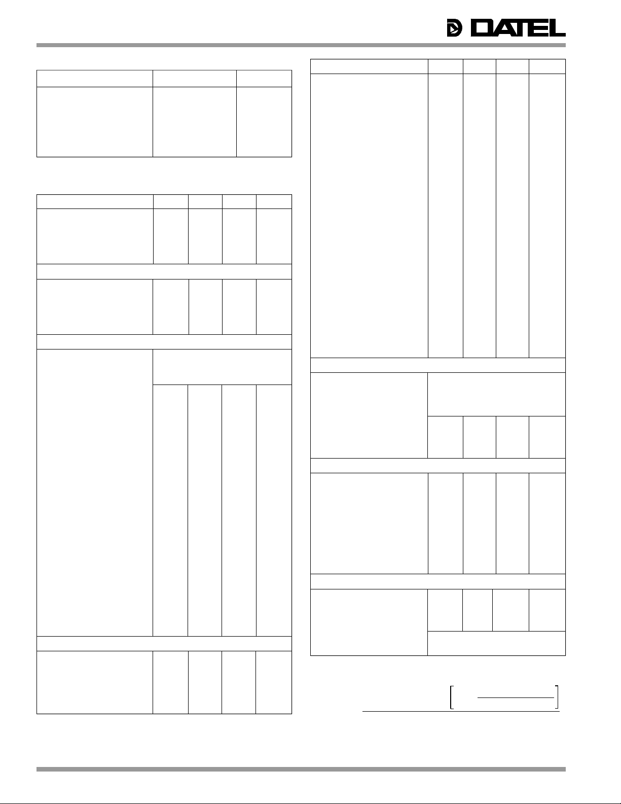
REGISTERREGISTER
3-STATE OUTPUT REGISTER
START CONVERT 16
DIGITAL CORRECTION LOGIC
+5V SUPPLY
+15V SUPPLY
ANALOG GROUND
DIGITAL GROUND
–15V SUPPLY
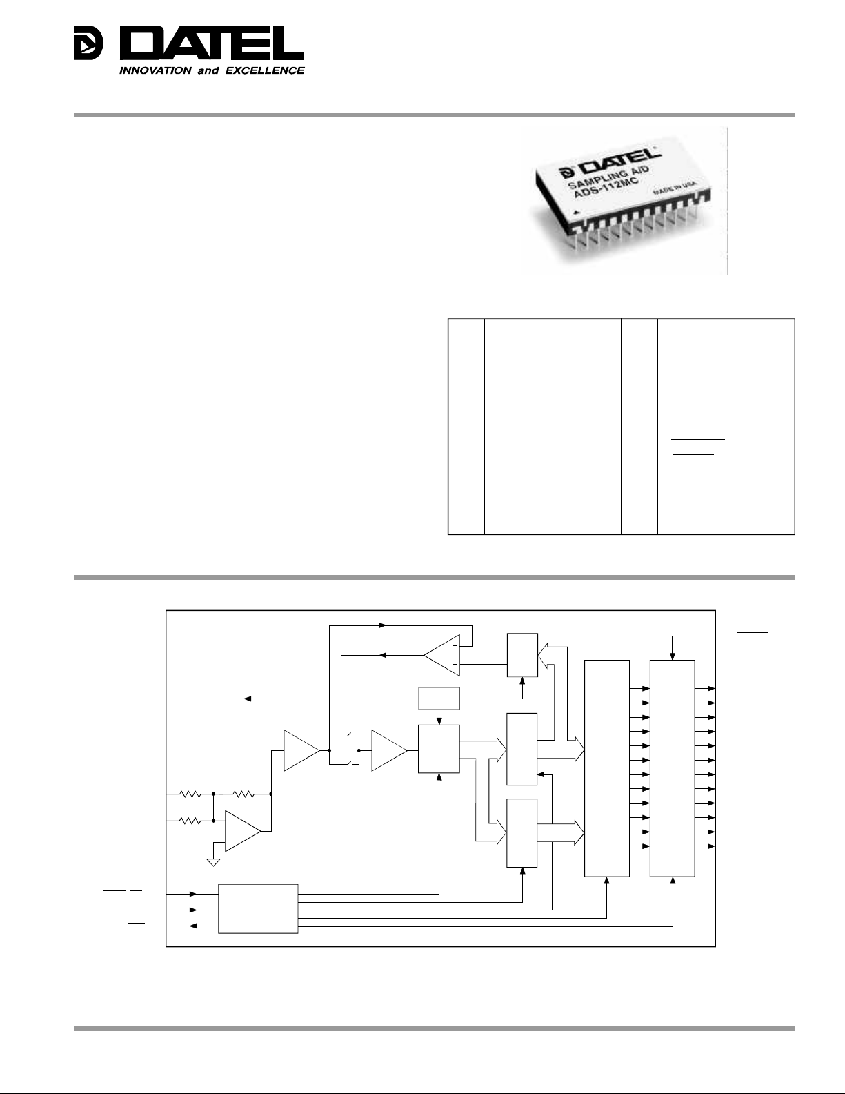
FEATURES
• 12-bit resolution
• No missing codes
• 1MHz minimum sampling rate
• Functionally complete
• Small 24-pin DDIP
• Low-power, 1.3 Watts
• Three-state output buffers
• Samples to Nyquist frequencies
ADS-112
12-Bit, 1MHz, Low-Power
Sampling A/D Converters
GENERAL DESCRIPTION
DATEL’s ADS-112 is a 12-bit, functionally complete, sampling
A/D converter that is packaged in a space-saving 24-pin DDIP.
Requiring ±15V and +5V supplies, a minimum sampling rate of
1MHz is achieved while only dissipating 1.3 Watts. The
ADS-112 digitizes signals up to Nyquist frequencies. Models
are available for use in either commercial (0 to + 70°C) or
military (–55 to +125°C) operating temperature ranges.
Typical applications include spectrum, transient, vibration and
waveform analysis. This device is also ideally suited for radar,
sonar, video digitization, medical instrumentation and highspeed data acquisition systems.
+10V REF. 21
S2
S/H
S1
BUFFER
BIPOLAR 20
ANALOG INPUT 19
–
+
INPUT/OUTPUT CONNECTIONS
PIN FUNCTION PIN FUNCTION
1 BIT 12 (LSB) 24 –15V SUPPLY
2 BIT 11 23 ANALOG GROUND
3 BIT 10 22 +15V SUPPLY
4 BIT 9 21 +10V REFERENCE
5 BIT 8 20 BIPOLAR
6 BIT 7 19 ANALOG INPUT
7 BIT 6 18 COMP BIN
8 BIT 5 17 ENABLE (1-12)
9 BIT 4 16 START CONVERT
10 BIT 3 15 EOC
11 BIT 2 14 DIGITAL GROUND
12 BIT 1 (MSB) 13 +5V SUPPLY
DAC
REF
FLASH
ADC
17 ENABLE (1-12)
12 BIT 1 (MSB)
11 BIT 2
10 BIT 3
9 BIT 4
8 BIT 5
7 BIT 6
6 BIT 7
5 BIT 8
4 BIT 9
3 BIT 10
2 BIT 11
1 BIT 12 (LSB)
COMP BIN 18
EOC 15
TIMING AND
CONTROL LOGIC
13
14
22
23
24
Figure 1. ADS-112 Functional Block Diagram
DATEL, Inc., 11 Cabot Boulevard, Mansfield, MA 02048-1151 (U.S.A.) • Tel: (508) 339-3000 Fax: (508) 339-6356 • For immediate assistance: (800) 233-2765
Page 2
ADS-112
® ®
ABSOLUTE MAXIMUM RATINGS
PARAMETERS LIMITS UNITS
+15V Supply (Pin 22) 0 to +18 Volts
–15V Supply (Pin 24) 0 to –18 Volts
+5V Supply (Pin 13) 0 to +6 Volts
Digital Inputs (Pin 16, 17, 18) –0.3 to +V
DD +0.3 Volts
Analog Input (Pin 19) –9 to +15 Volts
Lead Temp. (10 seconds) +300 °C
FUNCTIONAL SPECIFICATIONS
(TA = +25°C, ±VCC = ±15V, +VDD =+5V, 1MHz sampling rate, and a minimum 1 minute
warmup unless otherwise specified.)
ANALOG INPUTS MIN. TYP. MAX. UNITS
Input Voltage Range ➀
Bipolar — ±5 — Volts
Unipolar — 0 to +10 — Volts
Input Impedence 4.5 5 — kΩ
Input Capacitance — 6 15 pF
DIGITAL INPUTS
Logic Levels
Logic "1" +2.0 — — Volts
Logic "0" — — +0.8 Volts
Logic Loading "1" — — +10 µA
Logic Loading "0" — — –600 µA
PERFORMANCE
Resolution 12 Bits
No Missing Codes
in = 1MHz) Over the operating temperature range
(12 Bits; f
Integral Non-Linearity
+25°C — ±1/4 ±3/4 LSB
0°C to +70°C — ±1/4 ±3/4 LSB
–55°C to +125°C — ±1/2 ±1.5 LSB
Differential Non-Linearity
+25°C — ±1/4 ±3/4 LSB
0°C to +70°C — ±1/4 ±3/4 LSB
–55°C to +125°C — ±1/2 ±1 LSB
Full Scale Absolute Accuracy
+25°C — ±0.13 ±0.25 %FSR
0°C to +70°C — ±0.15 ±0.44 %FSR
–55°C to +125°C — ±0.25 ±0.78 %FSR
Unipolar Zero Error †
0°C to +70°C — ±0.074 ±0.265 %FSR
–55°C to +125°C — ±0.224 ±0.43 %FSR
Bipolar Zero Error †
0°C to +70°C — ±0.074 ±0.166 %FSR
–55°C to +125°C — ±0.124 ±0.210 %FSR
Bipolar Offset Error †
0°C to +70°C — ±0.1 ±0.38 %FSR
–55°C to +125°C — ±0.3 ±0.60 %FSR
Gain Error †
0°C to +70°C — ±0.1 ±0.38 %
–55°C to +125°C — ±0.3 ±0.60 %
Internal Reference Voltage, +25°C +9.98 +10.0 +10.02 Volts
Drift — ±5 ±30 ppm/°C
External Current — — 1.5 mA
DYNAMIC PERFORMANCE
In-Band Harmonics (–0.5dB)
dc to 100kHz — –81 –75 dB
100kHz to 500kHz — –75 –70 dB
Total Harm. Distort. (–0.5dB)
dc to 100kHz — –78 –75 dB
100kHz to 500kHz — –73 –68 dB
† See Tech Note 1
DYNAMIC PERF. (cont) MIN. TYP. MAX. UNITS
Signal-to-Noise Ratio
(wo/distort., –0.5dB)
dc to 100kHz 68 72 — dB
100kHz to 500kHz 67 71 — dB
Signal-to-Noise Ratio ➁
(& distort., –0.5dB)
dc to 100kHz 66 70 — dB
100kHz to 500kHz 66 70 — dB
Two-tone Intermodulation
Distortion (f
in = 75kHz,
s = 1MHz, –0.7dB) — –88 –80 dB
105kHz, f
Two-tone Intermodulation
Distortion (f
in = 480kHz,
s = 1MHz, –0.7dB) — –68 –65 dB
490kHz, f
Input Bandwith (–3dB)
Small Signal (–20dB input) 8 10 — MHz
Large Signal (–0.5dB input) 6 8 — MHz
Slew Rate — ±150 — V/µs
Apperture Delay TIme — — 20 ns
Effect. Aperture Delay Time — — 16 ns
Apperture Uncertainity (Jitter)
RMS — — 15 ps
Peak — — ±50 ps
Overvoltage Recovery Time — — 1000 ns
S/H Acquisition Time 160 250 280 ns
Conversion Rate
(Changing Inputs)
+25°C 1 — — MHz
0°C to +70°C 1 — — MHz
–55°C to +125°C 1 — — MHz
DIGITAL OUTPUTS
Output Coding
Pin 18 High
Pin 18 Low
Logic Level
Staight binary/Offset binary
Complementary binary
Complementary offset binary
Logic "1" +2.4 — — Volts
Logic "0" — — +0.4 Volts
Logic Loading "1" — — –160 µA
Logic Loading "0" — — +6.4 mA
POWER REQUIREMENTS
Power Supply Ranges ➂
+15V Supply +14.25 +15.0 +15.75 Volts
–15V Supply –14.25 –15.0 –15.75 Volts
+5V Supply +4.75 +5.0 +5.25 Volts
Power Supply Current
+15V Supply — +24 +35 mA
–15V Supply — –40 –48 mA
+5V Supply — +80 +95 mA
Power Dissipation — 1.3 1.7 Watts
Power Supply Rejection — — ±0.07 %FSR%V
PHYSICAL/ENVIRONMENTAL
Operating Temp. Range, Case
ADS-112MC 0 — +70 °C
ADS-112MM, 883 –55 — +125 °C
Storage Temperature Range –65 — +150 °C
Package Type 24-pin, metal-sealed, ceramic DDIP
Weight 0.42 ounces (12 grams)
➀ See Table 3 also
➁ Effective bits is equal to:
(SNR + Distortion) – 1.76 + 20 log
Full Scale Amplitude
Actual Input Amplitude
6.02
➂ For ±12V, +5V operation, contact DATEL
2
Page 3

® ®
Note: Scale is approximately 50ns per division.
ADS-112
TECHNICAL NOTES
1. Applications which are unaffected by endpoint errors or
remove them through software will use the typical connections shown in Figure 3. Remove system errors or adjust
the small initial errors of the ADS-112 to zero using the
optional external circuitry shown in Figure 4. The external
adjustment circuit has no effect on the throughput rate.
2. For best performance, always connect the analog and
digital ground pins to a ground plane beneath the converter.
The analog and digital grounds are not connected to each
other internally.
3. Bypass the analog and digital supplies and the +10V
reference (pin 21) to ground with 4.7µF, 25V tantalum
electrolytic capacitors in parallel with 0.1µF ceramic
capacitors. Bypass the +10V reference (pin 21) to analog
ground (pin 23).
4. Obtain straight binary/offset binary output coding by tying
COMP BIN (pin 18) to +5V or leaving it open. The device
N
START
CONVERT
150ns, ±25ns
has an internal pull-up resistor on this pin. To obtain
complementary binary or complementary offset binary
output coding, tie pin 18 to ground. The pin 18 signal is
compatible with CMOS/TTL logic levels for those users
desiring dynamic control of this function.
5. To enable the three-state outputs, connect ENABLE (pin 17)
to a logic "0" (low). To disable, connect pin 17 to a logic "1"
(high).
6. Do not change the status of pin 18 when EOC is high.
7. Re-initiating the START CONVERT (pin 16) while EOC is a
logic "1" (high) will result in a new conversion sequence.
TIMING
Figure 2 shows the relationship between the various input
signals. The timing shown applies over the operating
temperature range and over the operating power supply
range. These times are guaranteed by design.
N+1
INTERNAL S/H
EOC
OUTPUT
DATA
10ns min.
20ns max.
Hold
20ns max.
Conversion Time
600ns max.
DATA N-1 VALID
800ns min.
Figure 2. ADS-112 Timing Diagram
Acquisition Time
250ns
INVALID
DATA
200ns max.
60ns max.
35ns max.
DATA N VALID
INVALID
DATA
3
Page 4

ADS-112
For values of R1 and R2 refer to Table 3.
➀
® ®
CALIBRATION PROCEDURE
1. Connect the converter per Figures 3 and 4 and Tables 1 and
3 for the appropriate input range. Apply a pulse of 150
nanoseconds to the START CONVERT input (pin 16) at a
rate of 250kHz. This rate is chosen to reduce the flicker if
LED’s are used on the outputs for calibration purposes.
2. Zero Adjustments
Apply a precision voltage reference source between the
amplifier’s analog input and ground. Adjust the output of the
reference source per Table 2. For unipolar, adjust the zero
trimming potentiometer so that the output code flickers
equally between 0000 0000 0000 and 0000 0000 0001 with
COMP BIN (pin 18) tied high (straight binary) or between
1111 1111 1111 and 1111 1111 1110 with pin 18 tied low
(complementary binary).
For bipolar operation, adjust the potentiometer such that the
code flickers equally between 1000 0000 0000 and 1000
0000 0001 with pin 18 tied high (offset binary) or between
0111 1111 1111 and 0111 1111 1110 with pin 18 tied low
(complementary offset binary).
3. Full-Scale Adjustment
Set the output of the voltage reference used in step 2 to the
value shown in Table 2. Adjust the gain trimming potentiometer so that the output code flickers equally between 1111
1111 1110 and 1111 1111 1111 for pin 18 tied high or between
0000 0000 0001 and 0000 0000 0000 for pin 18 tied low.
To confirm proper operation of the device, vary the precision
reference voltage source to obtain the output coding listed
in Table 4.
Table 1. Input Range Selection
INPUT RANGE INPUT PIN TIE TOGETHER
±5v Pin 19 Pin 20 to Pin 21
0 to +10V Pin 19 Pin 20 to Ground
➀
R2
➀
R1
SIGNAL
INPUT
5k
Ω
50
Ω
GAIN
ADJUST
5kΩ
Figure 4. Optional Calibration Circuit
Table 2. Zero and Gain Adjust
+15V
–15V
10k
Ω
ZERO/
OFFSET
ADJUST
To Pin19
of ADS-112
Input Zero Adjust Gain Adjust
Range +1/2 LSB +FS – 1 1/2 LSB
0 to +10V +1.22mV +9.9963V
±5V +1.22mV +4.9963V
Table 3. Input Range (using external calibration)
INPUT RANGE R1 R2 UNIT
0 to 10V, ±5 2 2 kΩ
0 to 5V, ±2.5V 2 6 kΩ
0 to +2.5V, ±1.25V 2 14 kΩ
BIPOLAR
OPERATION
20
21
0.1µF
–15V
4.7µF
4.7µF
+15V
+5V
4.7µF
UNIPOLAR
OPERATION
20
21 +10V REF.
+
4.7µF
24
0.1µF
+
0.1µF
+
+
0.1µF
Figure 3. Typical ADS-112 Connection Diagram
23
22
13
14
Note: Always bypass pin 21 to ground
ADS-112
4
COMP BIN
12
11
10
9
8
7
6
5
4
3
2
1
15
17
16
19
18 +5V
BIT 1 (MSB)
BIT 2
BIT 3
BIT 4
BIT 5
BIT 6
BIT 7
BIT 8
BIT 9
BIT 10
BIT 11
BIT 12 (LSB)
EOC
ENABLE (1-12)
START CONVERT
ANALOG INPUT
Page 5

® ®
(fs = 1MHz, fin = 485kHz, Vin = –0.5dB, 4,096-point FFT)
Amplitude Relative to Full Scale (dB)
UNIPOLAR INPUT RANGE OUTPUT CODING INPUT RANGE BIPOLAR
SCALE 0 to +10V MSB LSB MSB LSB ±5V SCALE
+FS – 1 LSB +9.9976 1111 1111 1111 0000 0000 0000 +4.9976 +FS –1 LSB
+7/8 FS +8.7500 1110 0000 0000 0001 1111 1111 +3.7500 +3/4FS
+3/4 FS +7.5000 1100 0000 0000 0011 1111 1111 +2.5000 +1/2FS
+1/2 FS +5.0000 1000 0000 0000 0111 1111 1111 0.0000 0
+1/4 FS +2.5000 0100 0000 0000 1011 1111 1111 –2.5000 –1/2FS
+1/8 FS +1.2500 0010 0000 0000 1101 1111 1111 –3.7500 –3/4FS
+1 LSB +0.0024 0000 0000 0001 1111 1111 1110 –4.9976 –FS+1LSB
0 0.0000 0000 0000 0000 1111 1111 1111 –5.0000 –FS
–10
–20
–30
–40
–50
–60
–70
–80
–90
–100
–110
–120
–130
ADS-112
Table 4. Output Coding
STRAIGHT BIN. COMP. BINARY
OFF. BINARY COMP. OFF. BIN.
0
0 50 100 150 200 250 300 350 400 450 500
Frequency (kHz)
Figure 5. FFT Analysis of ADS-112
5
Page 6

ADS-112
ISO 9001
REGISTERED
® ®
MECHANICAL DIMENSIONS INCHES (mm)
1.31 MAX.
(33.27)
0.235 MAX.
0.190 MAX.
(4.826)
0.018 ±0.002
(5.969)
(0.457)
24
1 12
0.100 TYP.
(2.540)
1.100
(27.940)
PIN 1 INDEX
0.100
(2.540)
0.040
(1.016)
13
0.80 MAX.
(20.32)
0.200 MAX.
(5.080)
SEATING
PLANE
0.025
(0.635)
Dimension Tolerances
2 place decimal (.XX) ±0.010 (±0.254)
3 place decimal (.XXX) ±0.005 (±0.127)
Lead Material: Kovar alloy
Lead Finish:
over 100 microinches (nominal) nickel plating
50 microinches (minimum) gold plating
0.010
(0.254)
0.600 ±0.010
(15.240)
(unless otherwise indicated):
+0.002
–0.001
0.100
(2.540)
ORDERING INFORMATION
MODEL NUMBER OPERATING TEMP. RANGE
ADS-112MC 0 to +70°C
ADS-112MM –55 to +125°C
ADS-112/883 –55 to +125°C
For MIL-STD-883 product specification or availability of surface-mount packaging, contact DATEL. Receptacles for PC mounting
can be ordered through AMP Inc., Part # 3-331272-8 (Component Lead Socket), 24 required.
® ®
ACCESSORIES
ADS-EVAL4 Evaluation Board (without ADS-112)
HS-32 Heat Sink for all ADS-112 models
ISO 9001
DS-0149F 10/96
DATEL, Inc. 11 Cabot Boulevard, Mansfield, MA 02048-1151
Tel: (508) 339-3000 (800) 233-2765 Fax: (508) 339-6356
Internet: www.datel.com E-mail:sales@datel.com
Data Sheet Fax Back: (508) 261-2857
DATEL makes no representation that the use of its products in the circuits described herein, or the use of other technical information contained herein, will not infringe upon existing or future patent rights. The descriptions contained herein
do not imply the granting of licenses to make, use, or sell equipment constructed in accordance therewith. Specifications are subject to change without notice. The DATEL logo is a registered DATEL, Inc. trademark.
DATEL (UK) LTD. Tadley, England Tel: (01256)-880444
DATEL S.A.R.L. Montigny Le Bretonneux, France Tel: 1-34-60-01-01
DATEL GmbH München, Germany Tel: 89-544334-0
DATEL KK Tokyo, Japan Tel: 3-3779-1031, Osaka Tel: 6-354-2025
 Loading...