

Page 1
700 MHz to 1050 MHz Quadrature
V
V
Data Sheet
FEATURES
IQ demodulator with integrated fractional-N PLL
LO frequency range: 700 MHz to 1050 MHz
For the following specifications (LPEN = 0)/(LPEN = 1):
Input P1dB: 12.8 dBm/11.7 dBm
Input IP3: 26.7 dBm/24.0 dBm
Noise figure (DSB): 13.1 dB/12.4 dB
Voltage conversion gain: 1.0 dB/4.3 dB
Quadrature demodulation accuracy
Phase accuracy: <0.5°
Amplitude accuracy: <0.1 dB
Baseband demodulation: 170 MHz/135 MHz, 3 dB
bandwidth
SPI serial interface for PLL programming
40-lead, 6 mm × 6 mm LFCSP
APPLICATIONS
QAM/QPSK RF/IF demodulators
Cellular W-CDMA/CDMA/CDMA2000
Microwave point-to-(multi)point radios
Broadband wireless and WiMAX
Demodulator with Fractional-N PLL
ADRF6807
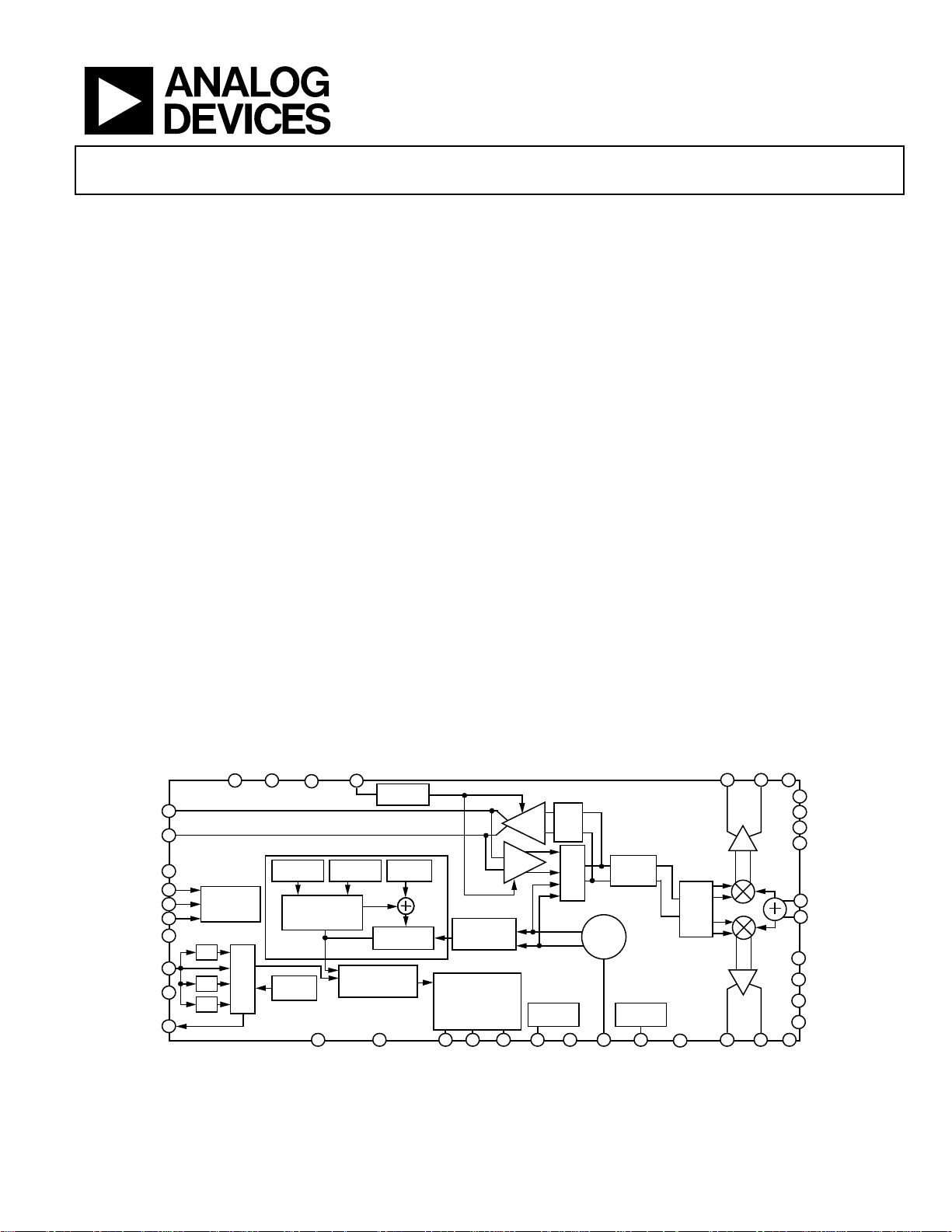
GENERAL DESCRIPTION
The ADRF6807 is a high dynamic range IQ demodulator with
integrated phase-locked loop (PLL) and voltage controlled
oscillator (VCO). The fractional-N PLL/synthesizer generates a
frequency in the range of 2.8 GHz to 4.2 GHz. A programmable
quadrature divider (divide ratio = 4) divides the output frequency
of the VCO down to the required local oscillator (LO) frequency to
drive the mixers in quadrature. Additionally, an output divider
(divide ratio = 4 to 8) generates a divided-down VCO signal for
external use.
The PLL reference input is supported from 9 MHz to 160 MHz.
The phase detector output controls a charge pump whose output
is integrated in an off-chip loop filter. The loop filter output is
then applied to an integrated VCO.
The IQ demodulator mixes the differential RF input with the
complex LO derived from the quadrature divider. The differential
I and Q output paths have excellent quadrature accuracy and
can handle baseband signaling or complex IF up to 120 MHz.
A reduced power mode of operation is also provided by
programming the serial interface registers to reduce current
consumption, with slightly degraded input linearity and output
current drive.
ADRF6807 is fabricated using an advanced silicon-germanium
The
BiCMOS process. It is available in a 40-lead, exposed paddle,
RoHS-compliant, 6 mm × 6 mm LFCSP package. Performance is
specified over the −40°C to +85°C temperature range.
FUNCTIONAL BLOCK DIAGRAM
CCLO
CCLO
GND
34
35
LON
37
38
LOP
MUX
FRACTION
REG
THIRD-ORDER
FRACTIONAL
INTERPOLATOR
TEMP
SENSOR
11
GND
12
DATA
13
CLK
14
LE
15
GND
6
REFIN
7
GND
MUXOUT
Rev. B
Information furnished by Analog Devices is believed to be accurate and reliable. However, no
responsibility is assumed by Anal og Devices for its use, nor for any infringements of patents or ot her
rights of third parties that may result from its use. Specifications subject to change without notice. No
license is granted by implication or otherwise under any patent or patent rights of Analog Devices.
Trademarks and registered trademarks are the property of their respective owners.
8
SPI
INTERFACE
×2
÷2
÷4
17
1
VCC1
LOSEL
36
MODULUS
–
+
FREQUENCY
DETECTOR
BUFFER
CTRL
INTEGER
REG
N COUNTER
PHASE
2
VCC1
PRESCALER
CHARGE PUMP
250µA,
500µA (DEFAULT),
750µA,
1000µA
3
CPOUT
÷2
4
GND
Figure 1.
GND
IBBNIBBP
3233
31
30
20
GND
29
28
27
26
25
24
23
22
21
GND
DECL3
VCCRF
GND
RFIN
RFIP
GND
VOCM
VCCBB
GND
BUFFER
RSET
BUFFER
9 105
DECL2 VCC2
DIV
÷4,
÷6,
÷8
MUX
VCO
CORE
39
VTUNE
ADRF6807
DIVIDER
÷2
VCO LDO2.5V LDO
40
DECL1
16
GND
QUAD
÷2
18
QBBP
19
QBBN
One Technology Way, P.O. Box 9106, Norwood, MA 02062-9106, U.S.A.
Tel: 781.329.4700 www.analog.com
Fax: 781.461.3113 ©2011–2012 Analog Devices, Inc. All rights reserved.
09993-001
Page 2

ADRF6807 Data Sheet
TABLE OF CONTENTS
Features.............................................................................................. 1
Applications....................................................................................... 1
General Description ......................................................................... 1
Functional Block Diagram .............................................................. 1
Revision History ............................................................................... 2
Specifications..................................................................................... 3
Timing Characteristics ................................................................ 5
Absolute Maximum Ratings............................................................ 6
ESD Caution.................................................................................. 6
Pin Configuration and Function Descriptions............................. 7
Typical Performance Characteristics ............................................. 9
Synthesizer/PLL.......................................................................... 12
Complementary Cumulative Distribution Functions
(CCDF) ........................................................................................13
Circuit Description......................................................................... 14
LO Quadrature Drive................................................................. 14
V-to-I Converter......................................................................... 14
Mixers .......................................................................................... 14
Emitter Follower Buffers ........................................................... 14
Bias Circuitry .............................................................................. 14
Register Structure....................................................................... 14
LO Divider Programming......................................................... 21
Programming Example.............................................................. 21
Applications Information.............................................................. 22
Basic Connections...................................................................... 22
Supply Connections................................................................... 22
Synthesizer Connections........................................................... 22
I/Q Output Connections........................................................... 23
RF Input Connections ............................................................... 23
Charge Pump/VTUNE Connections ...................................... 23
LO Select Interface ..................................................................... 23
External LO Interface ................................................................ 23
Setting the Frequency of the PLL............................................. 23
Register Programming............................................................... 23
EVM Measurements .................................................................. 24
Evaluation Board Layout and Thermal Grounding................... 25
ADRF6807 Software .................................................................. 30
Characterization Setups................................................................. 32
Outline Dimensions....................................................................... 36
Ordering Guide .......................................................................... 36
REVISION HISTORY
2/12—Rev. A to Rev. B
Changes to Table 1............................................................................ 3
Changes to Figure 21 and to Changes to Figure 24 Through
Figure 26 ..........................................................................................12
Changes to Figure 34...................................................................... 16
Changes to Figure 37...................................................................... 18
Changes to Figure 38...................................................................... 19
Changes to Figure 39...................................................................... 20
Changes to EVM Measurements Section and Changes to
Figure 42 ..........................................................................................24
Changes to Figure 43...................................................................... 25
Added Figure 44; Renumbered Sequentially .............................. 26
Changes to Figure 45 and Figure 46............................................. 27
Changes to Table 7.......................................................................... 29
Changes to Figure 47...................................................................... 30
Changes to Figure 48...................................................................... 31
9/11—Rev. 0 to Rev. A
Changes to EVM Measurements Section and Figure 42 ........... 24
8/11—Revision 0: Initial Version
Rev. B | Page 2 of 36
Page 3

Data Sheet ADRF6807
SPECIFICATIONS
VS1 (V
= 4.5 MHz, R
f
BB
differential RF input port impedance, all register and PLL settings use the recommended values shown in the Register Structure section,
unless otherwise noted.
Table 1.
Parameter Test Conditions/Comments Min Typ Max Unit
FREQUENCY RANGE 700 1050 MHz
RF INPUT at 900 MHz RFIP, RFIN pins
Input Return Loss Relative to 100 Ω −18 dB
Input P1dB LPEN = 0 (standard power mode) 12.8 dBm
LPEN = 1 (low power mode) 11.7 dBm
Second-Order Input Intercept (IIP2) LPEN = 0; −5 dBm each tone >65 dBm
LPEN = 1; −5 dBm each tone >65 dBm
Third-Order Input Intercept (IIP3) LPEN = 0; −5 dBm each tone 26.7 dBm
LPEN = 1; −5 dBm each tone 24.0 dBm
Noise Figure Double sideband from RF to either I or Q output; LPEN = 0 13.1 dB
Double sideband from RF to either I or Q output; LPEN = 1 12.4 dB
With a −5 dBm interferer 5 MHz away 16 dB
LO-to-RF Leakage At 1×LO frequency, 100 Ω termination at the RF port −73 dBm
I/Q BASEBAND OUTPUTS IBBP, IBBN, QBBP, QBBN pins
Voltage Conversion Gain
Demodulation Bandwidth 1 V p-p signal 3 dB bandwidth; LPEN = 0 170 MHz
1 V p-p signal 3 dB bandwidth; LPEN = 1 135 MHz
Quadrature Phase Error 0.35 Degrees
I/Q Amplitude Imbalance 0.05 dB
Output DC Offset (Differential) ±8 mV
Output Common-Mode Reference VOCM applied input voltage 1.55 1.65 1.75 V
Common-Mode Offset |(V
Gain Flatness Any 5 MHz 0.2 dB p-p
Maximum Output Swing Differential 450 Ω load 3 V p-p
Differential 200 Ω load 2.4 V p-p
Maximum Output Current Each pin 6 mA p-p
LO INPUT/OUTPUT LOP, LON
Output Level (LPEN = 0)
Output Level (LPEN = 1)
Input Level Externally applied 2×LO, PLL disabled 0 dBm
Input Impedance Externally applied 2×LO, PLL disabled 50 Ω
LO Main Divider
VCO Output Divider Range
VCO Operating Frequency 2800 4200 MHz
VCCB B
and V
) = 5 V, and VS2 (V
VCCRF
= 450 differential, RF port driven from a 1:2 balun to step up the 50 Ω source impedance to match the 100 Ω
LOAD
, V
VCC1
VCC2
, and V
) = 3.3 V; ambient temperature (TA) = 25°C; f
VCCLO
450 Ω differential load across IBBP, IBBN (or QBBP, QBBN);
= 26 MHz, fLO = 900 MHz,
REF
1 dB
LPEN = 0
450 Ω differential load across IBBP, IBBN (or QBBP, QBBN);
4.3 dB
LPEN = 1
+ V
IBBN
)/2 − V
IBBP
Into a differential 50 Ω load, LO buffer enabled (output
VOCM
|, |(V
QBBP
+ V
QBBN
)/2 − V
| 25 mV
VOCM
1 dBm
frequency = 800 MHz)
Into a differential 50 Ω load, LO buffer enabled (output
−0.75 dBm
frequency = 800 MHz)
VCO to mixer, including quadrature divider, see Tabl e 5 for
4
divider programming
VCO to (LOP, LON), see Tab le 6 for supported output divider
4 8
modes
Rev. B | Page 3 of 36
Page 4

ADRF6807 Data Sheet
Parameter Test Conditions/Comments Min Typ Max Unit
SYNTHESIZER SPECIFICATIONS
All synthesizer specifications measured with recommended
settings provided in Figure 33 through Figure 40
Channel Spacing f
PLL Bandwidth
SPURS
Reference Spurs f
f
f
f
PHASE NOISE (USING 67 kHz LOOP
FILTER)
= 26 MHz 25 kHz
PFD
Can be adjusted with off-chip loop filter component values
and R
SET
= 900 MHz, f
f
LO
baseband outputs with f
= 26 MHz, f
REF
/2 −104 dBc
REF
× 2 −85 dBc
REF
× 3 −97 dBc
REF
fLO = 900 MHz, f
baseband outputs with f
= 26 MHz, f
REF
= 26 MHz −93 dBc
PFD
= 26 MHz, f
REF
= 26 MHz, measured at
PFD
= 50 MHz
BB
= 26 MHz, measured at
PFD
= 50 MHz
BB
At 1 kHz offset −104 dBc/Hz
At 10 kHz offset −107 dBc/Hz
At 100 kHz offset −111 dBc/Hz
At 500 kHz offset −131 dBc/Hz
At 1 MHz offset −138 dBc/Hz
At 5 MHz offset −149 dBc/Hz
At 10 MHz offset −152 dBc/Hz
Integrated Phase Noise 1 kHz to 10 MHz integration bandwidth 0.13
Phase Detector Frequency 20 26 40 MHz
PHASE NOISE (USING 2.5 kHz
LOOP FILTER)
fLO = 900 MHz, f
= 26 MHz, f
REF
baseband outputs with f
= 26 MHz, measured at
PFD
= 50 MHz
BB
At 1 kHz offset −73 dBc/Hz
At 10 kHz offset −90 dBc/Hz
At 100 kHz offset −119 dBc/Hz
At 500 kHz offset −135 dBc/Hz
At 1 MHz offset −141 dBc/Hz
At 5 MHz offset −150 dBc/Hz
At 10 MHz offset −152 dBc/Hz
PLL FIGURE OF MERIT (FOM) Measured with f
Measured with f
= 26 MHz, f
REF
= 104 MHz, f
REF
= 26 MHz −215.4 dBc/Hz/Hz
PFD
= 26 MHz −220.9 dBc/Hz/Hz
PFD
Phase Detector Frequency 20 26 40 MHz
REFERENCE CHARACTERISTICS REFIN, MUXOUT pins
REFIN Input Frequency Usable range 9 160 MHz
REFIN Input Capacitance 4 pF
MUXOUT Output Level VOL (lock detect output selected) 0.25 V
V
(lock detect output selected) 2.7 V
OH
REFOUT Duty Cycle 50 %
CHARGE PUMP
Pump Current 500 μA
Output Compliance Range 1 2.8 V
LOGIC INPUTS CLK, DATA, LE pins
Input High Voltage, V
Input Low Voltage, V
Input Current, I
INH/IINL
1.4 3.3 V
INH
0 0.7 V
INL
0.1 μA
Input Capacitance, CIN 5 pF
67 kHz
°rms
Rev. B | Page 4 of 36
Page 5
Data Sheet ADRF6807
CLK
Parameter Test Conditions/Comments Min Typ Max Unit
POWER SUPPLIES VCC1, VCC2, VCCLO, VCCBB, VCCRF pins
Voltage Range (3.3 V) VCC1, VCC2, VCCLO 3.135 3.3 3.465 V
Voltage Range (5 V) VCCBB, VCCRF 4.75 5 5.25 V
Supply Current (3.3 V) (LPEN = 0) Normal Rx mode 170 mA
Rx mode with LO buffer enabled 227 mA
Supply Current (5 V) (LPEN = 0) Normal Rx mode 86 mA
Rx mode with LO buffer enabled 86 mA
Supply Current (3.3 V) (LPEN = 1) Normal Rx mode 166 mA
Rx mode with LO buffer enabled 214 mA
Supply Current (5 V) (LPEN = 1) Normal Rx mode 76 mA
Rx mode with LO buffer enabled 76 mA
Supply Current (5 V) Power-down mode 10 mA
Supply Current (3.3 V) Power-down mode 15 mA
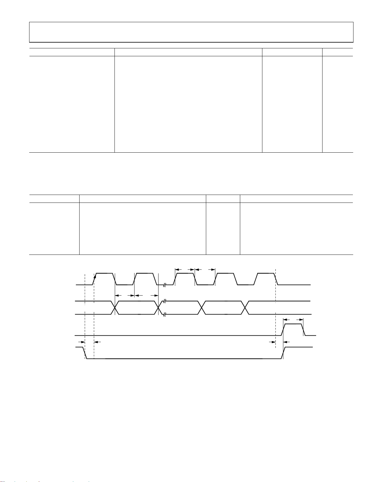
TIMING CHARACTERISTICS
VS1 (V
Table 2.
Parameter Limit at T
t1 20 ns min LE setup time
t2 10 ns min DATA to CLK setup time
t3 10 ns min DATA to CLK hold time
t4 25 ns min CLK high duration
t5 25 ns min CLK low duration
t6 10 ns min CLK to LE setup time
t7 20 ns min LE pulse width
VCCB B
and V
) = 5 V, and VS2 (V
VCCRF
MIN
, V
VCC2
, and V
VCC1
to T
Unit Test Conditions/Comments
MAX
VCCLO
) = 3.3 V.
t
4
t
5
DATA
DB23 (MSB) DB22
LE
t
1
LE
t
2
t
3
DB2
(CONTROL BIT C3)
DB1
(CONTROL BIT C2)
DB0 (LSB)
(CONTROL BIT C1)
t
6
t
7
09993-002
Figure 2. Timing Diagram
Rev. B | Page 5 of 36
Page 6
ADRF6807 Data Sheet
ABSOLUTE MAXIMUM RATINGS
Table 3.
Parameter Rating
Supply Voltage, VCCBB and VCCRF (VS1) −0.5 V to +5.5 V
Supply Voltage, VCC1, VCC2, and VCCLO (VS2) −0.5 V to +3.6 V
Digital I/O, CLK, DATA, and LE −0.3 V to +3.6 V
RFIP and RFIN (Each Pin AC-Coupled) 13 dBm
θJA (Exposed Paddle Soldered Down) 30°C/W
Maximum Junction Temperature 150°C
Operating Temperature Range −40°C to +85°C
Storage Temperature Range −65°C to +150°C
Stresses above those listed under Absolute Maximum Ratings
may cause permanent damage to the device. This is a stress
rating only; functional operation of the device at these or any
other conditions above those indicated in the operational
section of this specification is not implied. Exposure to absolute
maximum rating conditions for extended periods may affect
device reliability.
ESD CAUTION
Rev. B | Page 6 of 36
Page 7
Data Sheet ADRF6807
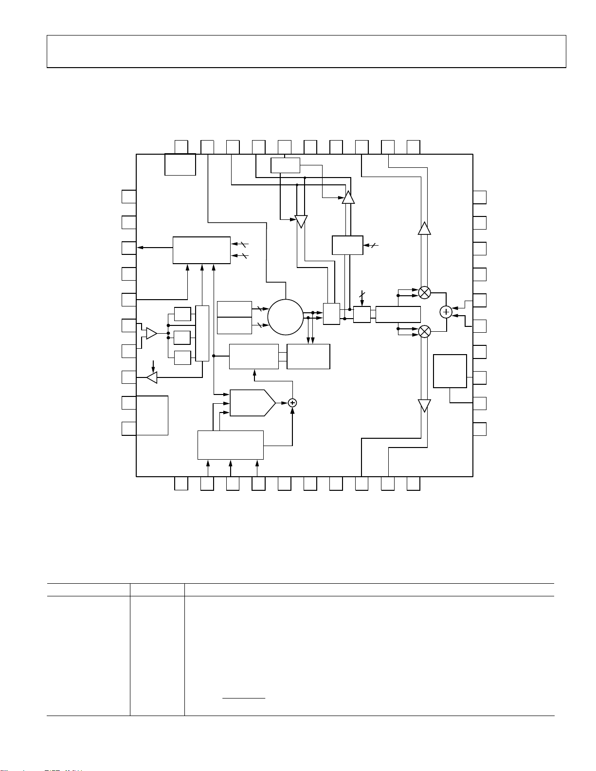
PIN CONFIGURATION AND FUNCTION DESCRIPTIONS
VCC1
VCC1
CPOUT
GND
RSET
REFIN
GND
MUXOUT
DECL2
VCC2
1
2
3
4
5
6
7
8
9
10
ADRF6807
ENABLE
2.5V
LDO
DECL1
VTUNE
40
39
VCO
LDO
PHASE DETEC TOR
AND
CHARGE PUM P
×2
÷2
MUX
÷4
FRACTIO N
LOP
38
SCALE
BLEED
VCO
BAND
CURRENT
CAL/SET
PROGRAMABLE
DIVIDER
THIRD-ORDER
SDM
MODULUS
SERIAL
PORT
6
6
LON
37
LOSEL
36
BUFFER
CTRL
VCO
2800MHz
TO
4200MHz
GND
35
PRESCALER
÷2
INTEGER
MUX
VCCLO
34
DIV
÷4, ÷6, ÷8
DIV
CTRL
DIV
÷2
33
IBBP
DIV
CTRL
QUADRATURE
IBBN
32
GND
31
30
GND
29
DECL3
28
VCCRF
27
GND
26
RFIN
÷2
COMMON-
MODE
LEVEL
CONTROL
25
RFIP
24
GND
23
VOCM
VCCBB
22
21
GND
11
12
13
14
15
16
17
LE
GND
NOTES
1. THE EXP OSED PADDLE SHOULD BE S OLDERED TO A LOW IMPEDANCE G ROUND PLANE.
CLK
DATA
GND
GND
VCCLO
18
QBBP
19
QBBN
20
GND
Figure 3. Pin Configuration
Table 4. Pin Function Descriptions
Pin No. Mnemonic Description
1, 2 VCC1 The 3.3 V Power Supply for VCO and PLL.
3 CPOUT Charge Pump Output Pin. Connect this pin to VTUNE through the loop filter.
4, 7, 11, 15, 16, 20,
GND Ground. Connect these pins to a low impedance ground plane.
21, 24, 27, 30, 31, 35
5 RSET
Charge Pump Current. The nominal charge pump current can be set to 250 μA, 500 μA, 750 μA, or 1 mA
using DB10 and DB11 of Register 4 and by setting DB18 to 0 (internal reference current). In this mode, no
external R
is required. If DB18 is set to 1, the four nominal charge pump currents (I
SET
externally tweaked according to the following equation where the resulting value is in units of ohms.
⎡
=
R
⎢
SET
⎣
I
NOMINAL
⎤
×
I
4.217
CP
⎥
8.37
−
⎦
Rev. B | Page 7 of 36
NOMINAL
09993-003
) can be
Page 8

ADRF6807 Data Sheet
Pin No. Mnemonic Description
6 REFIN Reference Input. Nominal input level is 1 V p-p. Input range is 9 MHz to 160 MHz.
8 MUXOUT
9 DECL2 Connect a 0.1 μF capacitor between this pin and ground.
10 VCC2 3.3 V Power Supply for 2.5 V LDO.
12 DATA Serial Data Input. The serial data is loaded MSB first with the three LSBs being the control bits.
13 CLK
14 LE
17, 34 VCCLO 3.3 V Power Supply for LO Path Blocks.
18, 19 QBBP, QBBN Demodulator Q-Channel Differential Baseband Outputs (Differential Output Impedance of 28 Ω).
22 VCCBB 5 V Power Supply for Demodulator Blocks.
23 VOCM
25, 26 RFIP, RFIN Differential 100 Ω, Internally Biased RF Inputs. These pins must be ac-coupled.
28 VCCRF 5 V Power Supply for Demodulator Blocks.
29 DECL3 Connect a 2.2 μF capacitor between this pin and ground.
32, 33 IBBN, IBBP Demodulator I-Channel Differential Baseband Outputs (Differential Output Impedance of 28 Ω).
36 LOSEL
37, 38 LON, LOP
39 VTUNE
40 DECL1
EP Exposed Paddle. The exposed paddle should be soldered to a low impedance ground plane.
Multiplexer Output. This output can be programmed to provide the reference output signal or the
lock detect signal. The output is selected by programming the appropriate register.
Serial Clock Input. This serial clock is used to clock in the serial data to the registers. The data is
latched into the 24-bit shift register on the CLK rising edge. Maximum clock frequency is 20 MHz.
Load Enable. When the LE input pin goes high, the data stored in the shift registers is loaded into
one of the six registers, the relevant latch being selected by the first three control bits of the 24-bit word.
Baseband Common-Mode Reference Input; 1.65 V Nominal. It sets the dc common-mode level of
the IBBx and QBBx outputs.
LO Select. Connect this pin to ground for the simplest operation and to completely control the LO
path and input/output direction from the register programming of the SPI.
For additional control without register reprogramming, this input pin can determine whether the
LOP and LON pins operate as inputs or outputs. LOP and LON become inputs if the LOSEL pin is set
low, the LDRV bit of Register 5 is set low, and the LXL bit of Register 5 is set high. The externally
applied LO drive must be at M×LO frequency (where M corresponds to the main LO divider setting). LON
and LOP become outputs when LOSEL is high or if the LDRV bit of Register 5 (DB3) is set high and
the LXL bit of Register 5 (DB4) is set to low. The output frequency is controlled by the LO output
divider bits in Register 7. This pin should not be left floating.
Local Oscillator Input/Output (Differential Output Impedance of 28 Ω). When these pins are used as
output pins, a differential frequency divided version of the internal VCO is available on these pins.
When the internal LO generation is disabled, an external M×LO frequency signal can be applied to
these pins, where M corresponds to the main divider setting.
VCO Control Voltage Input. This pin is driven by the output of the loop filter. The nominal input
voltage range on this pin is 1.0 V to 2.8 V.
Connect a 10 μF capacitor between this pin and ground as close to the device as possible because
this pin serves as the VCO supply and loop filter reference.
Rev. B | Page 8 of 36
Page 9
Data Sheet ADRF6807
A
R
A
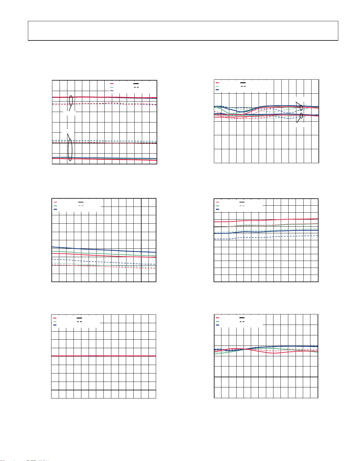
TYPICAL PERFORMANCE CHARACTERISTICS
VS1 = 5 V, VS2 = 3.3 V, TA = 25°C, RF input balun loss is de-embedded, unless otherwise noted. LO = 700 MHz to 1050 MHz;
Mini-Circuits ADTL2-18 balun on RF inputs.
16
14
12
10
CONVERSION GAIN (dB) AND INPUT P1dB (dBm)
IP1dB
8
GAIN
6
4
2
0
700
750
800
725
775
850
825
LO FREQUENCY (MHz)
875
T = +85°C
T = +25°C
T = –40°C
900
925
950
975
Figure 4. Conversion Gain and Input P1dB vs. LO Frequency
40
T = +85°C
T = +25°C
38
T = –40°C
36
34
32
30
28
INPUT IP3 (dBm)
26
24
22
20
700
750
725
LPEN = 0
LPEN = 1
800
775
825
LO FREQ UENCY (MHz)
850
875
900
925
950
975
1000
Figure 5. Input IP3 vs. LO Frequency
1.0
T = +85°C
T = +25°C
0.8
T = –40°C
0.6
0.4
0.2
TCH (dB)
0
–0.2
–0.4
IQ GAIN MISM
–0.6
–0.8
–1.0
700
750
725
LPEN = 0
LPEN = 1
800
775
825
LO FREQ UENCY (MHz)
850
875
900
925
950
975
1000
Figure 6. IQ Gain Mismatch vs. LO Frequency
LPEN = 0
LPEN = 1
1000
1025
1025
1025
1050
1050
1050
09993-004
09993-005
09993-006
80
T = +85°C
T = +25°C
T = –40°C
75
70
65
INPUT IP2 (dBm)
60
55
50
700
750
725
I CHANNEL
Q CHANNEL
800
775
825
LO FREQUENCY (MHz)
850
875
900
925
Figure 7. Input IP2 vs. LO Frequency
17
T = +85°C
16
T = +25°C
T = –40°C
15
14
13
12
11
10
9
NOISE FIG URE (dB)
8
7
6
5
700
750
725
LPEN = 0
LPEN = 1
800
775
825
LO FREQUENCY (MHz)
850
875
900
925
Figure 8. Noise Figure vs. LO Frequency
2.0
–0.5
TURE PHASE ERRO R (Degrees)
–1.0
–1.5
IQ QUAD
–2.0
1.5
1.0
0.5
0
700
T = +85°C
T = +25°C
T = –40°C
750
725
LPEN = 0
LPEN = 1
800
775
825
LO FRE QUENCY (MHz)
850
875
900
925
Figure 9. IQ Quadrature Phase Error vs. LO Frequency
LPEN = 1
LPEN = 0
950
950
950
975
975
975
1000
1000
1000
1025
1025
1025
1050
1050
1050
09993-007
09993-008
09993-009
Rev. B | Page 9 of 36
Page 10
ADRF6807 Data Sheet
–
–
–
50
LPEN = 0
LPEN = 1
–55
–60
–65
–70
–75
–80
LO-TO-RF FEEDTHROUGH (dBm)
–85
–90
700
750
800
850
900
950
1000
725
775
825
LO FREQ UENCY (MHz)
875
925
975
1025
1050
Figure 10. LO-to-RF Feedthrough vs. LO Frequency, LO Output Turned Off
40
–45
–50
–55
–60
–65
–70
LO-TO-BB FEEDTHROUGH ( dBV rms)
–75
–80
700 750 800 850 900 950 1000 1050
LO FRE QUENCY (MHz)
LPEN = 0
LPEN = 1
Figure 11. LO-to-BB Feedthrough vs. LO Frequency, LO Output Turned Off
30
–35
–40
–45
–50
–55
–60
RF-TO-BB FEEDTHROUGH (d Bc)
–65
–70
700 750 800 850 900 950 1000 1050
RF FREQ UENCY (MHz)
LPEN = 0
LPEN = 1
Figure 12. RF-to-BB Feedthrough vs. RF Frequency
09993-010
09993-111
09993-112
1
0
–1
–2
–3
–4
–5
–6
–7
–8
NORMALIZED BASEBAND
–9
FREQUENC Y RESPONSE (d B)
–10
–11
–12
110100
BASEBAND FREQ UENC Y (MHz)
LPEN = 0
LPEN = 1
Figure 13. Normalized BB Frequency Response
80
70
60
50
40
30
AND INPUT IP 3 (dBm)
20
INPUT P1dB (dBm), INPUT IP2 (dBm),
10
0
5 101520253035404550
LPEN = 0
LPEN = 0
LPEN = 0
LPEN = 1
LPEN = 1
LPEN = 1
BASEBAND FREQUE NCY (M Hz)
IIP2
TA = +85°C
= +25°C
T
A
TA = –40°C
IIP3
IP1dB
I CHANNEL
Q CHANNEL
Figure 14. Input P1dB, Input IP2, and Input IP3 vs. BB Frequency
30
LPEN = 0
LPEN = 1
28
26
24
22
20
18
16
NOISE F IGURE (dB)
14
12
10
8
–30 –25 –20 –15 –10 –5 0 5 10
INPUT BLOCKER POWER (dBm)
Figure 15. Noise Figure vs. Input Blocker Power,
= 900 MHz (RF Blocker 5 MHz Offset)
f
LO
400
09993-013
09993-014
09993-115
Rev. B | Page 10 of 36
Page 11
Data Sheet ADRF6807
A
0
–2
–4
–6
–8
–10
–12
–14
–16
–18
–20
RF RETURN LOSS (dB)
–22
–24
–26
–28
–30
700
750
800
850
900
725
775
825
RF FREQ UENCY (MHz)
875
925
950
975
Figure 16. RF Input Return Loss vs. RF Frequency,
Measured Through ADTL2-18 2-to-1 Input Balun
0
–2
–4
–6
–8
–10
–12
–14
–16
–18
–20
–22
–24
LO OUT PUT RETURN LO SS (dB)
–26
–28
–30
350
450
550
650
750
400
500
600
LO OUT PUT FREQ UENCY (MHz)
700
800
850
900
Figure 17. LO Output Return Loss vs. LO Output Frequency,
LO Output Enabled (350 MHz to 1050 MHz)
260
T = +85°C
T = +25°C
235
T = –40°C
LPEN = 0
LPEN = 1
210
185
3.3V SUPP LY
1000
950
1025
1000
1050
1050
09993-016
09993-017
2.0
LPEN = 0
LPEN = 1
1.9
1.8
1.7
1.6
T V OLTA GE ( V)
1.5
VPT
1.4
1.3
1.2
–40 –20 0 20 40 60 80
TEMPERATURE (°C)
09993-019
Figure 19. VPTAT Voltage vs. Temperature
3.5
TA = +85°C
= +25°C
T
A
= –40°C
T
A
3.0
2.5
2.0
1.5
VTUNE VOLTAGE (V)
1.0
0.5
350 370 390 410 430 450 470 490 510
LO FRE QUENCY (MHz)
09993-020
Figure 20. VTUNE Voltage vs. LO Frequency, Measured at the LO Output Pins
with LO Output in Divide-by-8 Mode
160
135
CURRENT (mA)
110
85
60
700
750
725
775
Figure 18. 5 V and 3.3 V Supply Currents vs. LO Frequency,
5V SUPPLY
800
850
825
875
LO FREQ UENCY (MHz)
LO Output Disabled
900
925
950
975
1000
1025
1050
09993-018
Rev. B | Page 11 of 36
Page 12

ADRF6807 Data Sheet
–
A
–
–
A
–
–
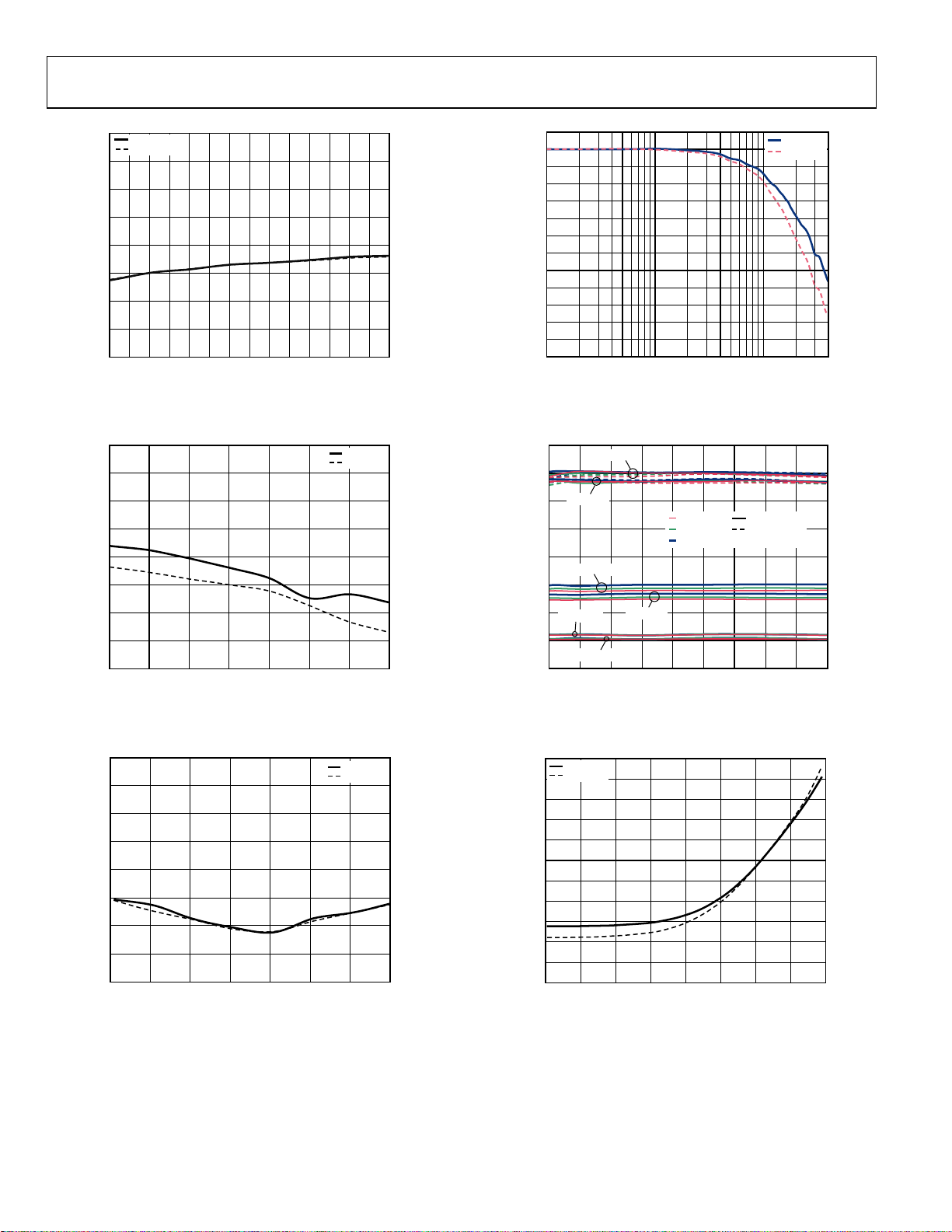
SYNTHESIZER/PLL
VS1 = 5 V, VS2 = 3.3 V, see the Register Structure section for recommended settings used. External loop filter bandwidth of ~67 kHz,
f
= f
REF
= 26 MHz, measured at BB output, fBB = 50 MHz, unless otherwise noted.
PFD
60
–70
–80
–90
–100
–110
67kHz LOOP FILTER
–120
SE NOISE (dBc/Hz)
–130
PH
–140
–150
–160
1k 10k 100k 1M 10M
2.5kHz LOOP FILTER
OFFSET FREQUENCY (Hz)
Figure 21. Phase Noise vs. Offset Frequency, f
TA=+85°C
= +25°C
T
A
= –40°C
T
A
= 900 MHz
LO
09993-021
70
TA= +85°C
T
= +25°C
A
–75
T
= –40°C
A
–80
–85
–90
–95
–100
PLL REFERENCE SPURS (dBc)
–105
–110
700 750 800 850 900 950 1000 1050
1× PFD FREQ UENCY
3× PFD FREQ UENCY
0.5× PFD FREQ UENCY
LO FREQUENCY (MHz)
09993-022
Figure 22. PLL Reference Spurs vs. LO Frequency
70
TA= +85°C
= +25°C
T
A
PLL REFERENCE SPURS (dBc)
–75
–80
–85
–90
–95
–100
–105
–110
=–40°C
T
A
700 750 800 850 900 950 1000 1050
2× PFD FREQ UENCY
4× PFD FREQ UENCY
LO FREQUENCY (MHz)
09993-023
Figure 23. PLL Reference Spurs vs. LO Frequency
2.0
TA=+85°C
T
=+25°C
A
T
= –40°C
A
0
700 750 800 850 900 950 1000 1050
LO FREQ UENCY (MHz)
09993-024
TED PHASE NOISE (°rms)
INTEGR
1.8
1.6
1.4
1.2
1.0
0.8
0.6
0.4
0.2
Figure 24. Integrated Phase Noise vs. LO Frequency (Spurs Omitted)
60
1kHz OFFSET
1kHz OFFSET
TA= +85°C
= +25°C
T
A
= –40°C
T
A
700 750 800 850 900 950 1000 1050
67kHz LOOP FILTER BANDWIDTH
2.5kHz LO OP FIL TER BANDWI DTH
LO FRE QUENCY (MHz)
10kHz O FFSET
10kHz OFFSET
5MHz OFFSET
09993-025
PHASE NOISE (dBc/Hz)
–70
–80
–90
–100
–110
–120
–130
–140
–150
–160
Figure 25. Phase Noise vs. LO Frequency (1 kHz, 10 kHz, and 5 MHz Offsets)
80
TA=+85°C
T
= +25°C
A
T
= –40°C
A
700 750 800 850 900 950 1000 1050
PHASE NOISE (dBc/Hz)
–90
–100
–110
–120
–130
–140
–150
–160
67kHz LOO P FILT ER BANDWIDT H
2.5kHz LOOP FIL TER BANDWI DTH
100kHz OFFSET
100kHz OFFSET
1MHz OFFSET
LO FREQ UENCY (MHz)
09993-026
Figure 26. Phase Noise vs. LO Frequency (100 kHz and 1 MHz Offsets)
Rev. B | Page 12 of 36
Page 13

Data Sheet ADRF6807
A
A
A
A
A
A
COMPLEMENTARY CUMULATIVE DISTRIBUTION FUNCTIONS (CCDF)
VS1 = 5 V, VS2 = 3.3 V, fLO = 900 MHz, fBB = 4.5 MHz.
100
90
80
70
60
50
40
30
TIVE DI STRIBUT ION PERCENTAGE (%)
20
10
CUMUL
0
02468101214
GAIN (d B) AND INPUT P1dB (d Bm)
T = +85°C
T = +25°C
T = –40°C
GAIN
LPEN = 0
LPEN = 1
IP1dB
09993-027
Figure 27. Gain and Input P1dB
100
T = +85°C
T = +25°C
90
T = –40°C
I CHANNEL
80
Q CHANNEL
70
60
50
40
30
TIVE DI STRIBUTI ON PERCENTAGE (%)
20
10
CUMUL
0
20 21 22 23 24 25 26 27 28 29 30
LPEN = 1
INPUT IP3 (dBm)
LPEN = 0
09993-028
Figure 28. Input IP3
100
T = +85°C
T = +25°C
90
T = –40°C
80
70
60
50
40
30
TIVE DIS TRIBUTION PERCENTAGE (%)
20
10
CUMUL
0
–1.0 –0.8 –0. 6 –0.4 –0.2 0 0.2 0.4 0.6 0.8 1.0
LPEN = 0
LPEN = 1
IQ GAIN MISMATCH (dB)
09993-129
Figure 29. IQ Gain Mismatch
100
90
80
70
60
50
40
30
TIVE DISTRIBUTION PERCENTAGE (%)
20
10
CUMUL
0
50 55 60 65 70 75 80
LPEN = 0
INPUT IP2 (dBm)
LPEN = 1
Figure 30. Input IP2
100
T = +85°C
T = +25°C
90
T = –40°C
80
LPEN = 0
LPEN = 1
70
60
50
40
30
TIVE DI STRIBUTI ON PERCENTAGE (%)
20
10
CUMUL
0
6 7 8 9 10 11 12 13 14 15 16 17 18 19
NOISE FIGURE (d B)
Figure 31. Noise Figure
100
T = +85°C
T = +25°C
90
T = –40°C
80
70
60
50
40
30
TIVE DISTRIBUTION PERCENTAGE (%)
20
10
CUMUL
0
–2.0 –1.5 –1.0 –0.5 0 0.5 1.0 1.5 2. 0
LPEN = 0
LPEN = 1
IQ QUADRATURE PHASE ERRO R (Degrees)
Figure 32. IQ Quadrature Phase Error
09993-030
09993-029
09993-132
Rev. B | Page 13 of 36
Page 14

ADRF6807 Data Sheet
CIRCUIT DESCRIPTION
The ADRF6807 integrates a high performance IQ demodulator
with a state-of-the-art fractional-N PLL. The PLL also integrates
a low noise VCO. The SPI port allows the user to control the
fractional-N PLL functions, the demodulator LO divider functions,
and optimization functions, as well as allowing for an externally
applied LO.
The ADRF6807 uses a high performance mixer core that results
in an exceptional input IP3 and input P1dB, with a very low output
noise floor for excellent dynamic range.
LO QUADRATURE DRIVE
A signal at 2× the desired mixer LO frequency is delivered to
a divide-by-2 quadrature phase splitter followed by limiting
amplifiers, which then drive the I and Q mixers, respectively.
V-TO-I CONVERTER
The differential RF input signal is applied to a V-to-I converter
that converts the differential input voltage to output currents. The
V-to-I converter provides a differential 100 Ω input impedance.
The V-to-I bias current can be reduced by putting the device in
low power mode (setting LPEN = 1 by setting Register 5, DB5 = 1).
Generally with LPEN = 1, input IP3 and input P1dB degrade,
but the noise figure is slightly better. Overall, the dynamic range
is reduced by setting LPEN = 1.
MIXERS
The ADRF6807 has two double-balanced mixers: one for the inphase channel (I channel) and one for the quadrature channel
(Q channel). These mixers are based on the Gilbert cell design
of four cross-connected transistors. The output currents from
the two mixers are summed together in the resistive loads that
then feed into the subsequent emitter follower buffers. When
the part is put into its low power mode (LPEN = 1), the mixer
core load resistors are increased, which does increase the gain by
roughly 3 dB; however, as previously stated in the V-to -I
Converter section, the overall dynamic range does decrease
slightly.
EMITTER FOLLOWER BUFFERS
The output emitter followers drive the differential I and Q
signals off chip. The output impedance is set by on-chip 14 Ω
series resistors that yield a 28 Ω differential output impedance
for each baseband port. The fixed output impedance forms a
voltage divider with the load impedance that reduces the effective
gain. For example, a 500 Ω differential load has ~0.5 dB lower
effective gain than a high (10 kΩ) differential load impedance.
The common-mode dc output levels of the emitter follower outputs
are set by the voltage applied to the VOCM pin. The VOCM pin
must be driven with a voltage (typically 1.65 V) for the emitter
follower buffers to function. If the VOCM pin is left open, the
emitter follower outputs do not bias up properly.
BIAS CIRCUITRY
There are several band gap reference circuits and two low
dropout regulators (LDOs) in the ADRF6807 that generate the
reference currents and voltages used by different sections. One of
the LDOs is the 2.5V_LDO, which is always active and provides
the 2.5 V supply rail used by the internal digital logic blocks.
The 2.5V_LDO output is connected to the DECL2 pin (Pin 9)
for the user to provide external decoupling. The other LDO is
the VCO_LDO, which acts as the positive supply rail for the
internal VCO. The VCO_LDO output is connected to the DECL1
pin (Pin 40) for the user to provide external decoupling. The
VCO_LDO can be powered down by setting Register 6, DB18 = 0,
which allows the user to save power when not using the VCO.
Additionally, the bias current for the mixer V-to-I stage, which
drives the mixer core, can be reduced by putting the device in
low power mode (setting LPEN = 1 by setting Register 5, DB5 = 1).
REGISTER STRUCTURE
The ADRF6807 provides access to its many programmable features
through a 3-wire SPI control interface that is used to program
the seven internal registers. The minimum delay and hold times
are shown in the timing diagram (see Figure 2). The SPI provides
digital control of the internal PLL/VCO as well as several other
features related to the demodulator core, on-chip referencing,
and available system monitoring functions. The MUXOUT pin
provides a convenient, single-pin monitor output signal that can
be used to deliver a PLL lock-detect signal or an internal voltage
proportional to the local junction temperature.
Note that internal calibration for the PLL must run when the
ADRF6807 is initialized at a given frequency. This calibration is
run automatically whenever Register 0, Register 1, or Register 2 is
programmed. Because the other registers affect PLL performance,
Register 0, Register 1, and Register 2 must always be programmed
last. For ease of use, starting the initial programming with
Register 7 and then programming the registers in descending
order ending with Register 0 is recommended. Once the PLL
and other settings are programmed, the user can change the
PLL frequency simply by programming Register 0, Register 1,
or Register 2 as necessary.
Rev. B | Page 14 of 36
Page 15

Data Sheet ADRF6807
DIVIDE
MODE
DB23 DB22 DB21 DB20 DB19 DB18 DB17 DB16 DB15 DB14 DB13 DB12 DB11 DB10 DB9 DB8 DB7 DB6 DB5 DB4 DB3 DB2 DB1 DB0
0000000000000DMID6ID5ID4ID3ID2ID1ID0C3(0)C2(0)C1(0)
DM
DIVIDE MODE
0
FRACTIO NAL (DEFAUL T)
1
INTEGER
INTEGE R DIVIDE RAT IO CONTROL BITS
Figure 33. Integer Divide Control Register (R0)
Register 0—Integer Divide Control
With R0[2:0] set to 000, the on-chip integer divide control register
is programmed as shown in Figure 33. The internal VCO
frequency (f
f
VCO
) equation is
VCO
= f
× (INT + (FRAC/MOD)) × 2 (1)
PFD
where:
f
is the output frequency of the internal VCO.
VCO
INT is the preset integer divide ratio value (21 to 123 for integer
mode, 24 to 119 for fractional mode).
FRAC is the preset fractional divider ratio value (0 to MOD − 1).
MOD is the preset fractional modulus (1 to 2047).
ID6 ID5 ID4 ID3 ID2 ID1 ID0
0010101
0010110
0010111
0011000
... ... ... ... ... ... ...
... ... ... ... ... ... ...
0111000
... ... ... ... ... ... ...
... ... ... ... ... ... ...
1110111
1111000
1111001
1111010
1111011
DIVIDE RAT IO
21 (INTEGER MODE ONLY)
22 (INTEGER MODE ONLY)
23 (INTEGER MODE ONLY)
24
...
...
56 (DEFAULT )
...
...
119
120 (INTEGER MODE ONLY)
121 (INTEGER MODE ONLY)
122 (INTEGER MODE ONLY)
123 (INTEGER MODE ONLY)
The integer divide ratio sets the INT value in Equation 1. The
INT, FRAC, and MOD values make it possible to generate output
frequencies that are spaced by fractions of the PFD frequency.
Note that the demodulator LO frequency is given by f
LO
where M is the programmed LO main divider (see Table 5 ).
Divide Mode
Divide mode determines whether fractional mode or integer mode
is used. In integer mode, the VCO output frequency, f
calculated by
f
= f
VCO
× (INT) × 2 (2)
PFD
= f
VCO
VCO
, is
/M,
09993-031
Rev. B | Page 15 of 36
Page 16

ADRF6807 Data Sheet
Register 1—Modulus Divide Control
With R1[2:0] set to 001, the on-chip modulus divide control register is programmed as shown in Figure 34. The MOD value is the preset
fractional modulus ranging from 1 to 2047.
MODULUS DIVIDE RATIO
DB23 DB22 DB21 DB20 DB19 DB18 DB17 DB16 DB15 DB14 DB13 DB12 DB11 DB10 DB9 DB8 DB7 DB6 DB5 DB4 DB3 DB2 DB1 DB0
0 0 0 0 0 0 0 0 0 0 MD10 MD9 MD8 MD7 MD6 MD5 MD4 MD3 MD2 MD1 MD0 C3(0) C2(0) C1(1)
CONTROL BITS
MD10 MD9 MD8 MD7 MD6 MD5 MD4 MD3 MD2 MD1 MD0
0 0000000001
0 0000000010
... ... ... ... ... ... ... ... ... ... ...
... ... ... ... ... ... ... ... ... ... ...
1 1000000000
... ... ... ... ... ... ... ... ... ... ...
... ... ... ... ... ... ... ... ... ... ...
1 1111111111
MODULUS VALUE
1
2
...
...
1536 (DEFAUL T)
...
...
2047
Figure 34. Modulus Divide Control Register (R1)
Register 2—Fractional Divide Control
With R2[2:0] set to 010, the on-chip fractional divide control register is programmed as shown in Figure 35. The FRAC value is the preset
fractional modulus ranging from 0 to MOD − 1.
FRACTIONAL DIVI DE RATIO
DB23 DB22 DB21 DB20 DB19 DB18 DB17 DB16 DB15 DB14 D B13 DB12 DB 11 DB10 DB9 DB8 DB7 DB6 DB5 DB4 DB3 DB2 DB1 DB0
0000000000FD10FD9FD8FD7FD6FD5FD4FD3FD2FD1FD0C3(0)C2(1)C1(0)
FD10 FD9 FD8 FD7 FD6 FD5 FD4 FD3 FD2 FD1 FD0
0 0000000000
0 0000000001
... ... ... ... ... ... ... ... ... ... ...
... ... ... ... ... ... ... ... ... ... ...
0 1100000000
... ... ... ... ... ... ... ... ... ... ...
... ... ... ... ... ... ... ... ... ... ...
FRACTIONAL VALUE MUST BE LESS THAN MODULUS
Figure 35. Fractional Divide Control Register (R2)
CONTROL BITS
FRACTIO NAL VALUE
0
1
...
...
768 (DEFAUL T)
...
...
<MDR
Register 3—Sigma Delta (Σ-Δ) Modulator Dither Control
With R3[2:0] set to 011, the on-chip Σ- modulator dither control register is programmed as shown in Figure 36. The dither restart value
can be programmed from 0 to 217, though a value of 1 is typically recommended.
DITHER
MAGNITUDE
DB23 DB22 DB21 DB20 DB19 DB18 DB17 DB16 DB15 DB14 DB13 DB12 DB11 DB10 DB9 DB8 DB7 DB6 DB5 DB4 DB3 DB2 DB1 DB0
0 DITH1 DI TH0 DEN DV16 DV15 DV14 DV13 DV12 DV11 DV10 DV9 DV8 DV7 DV6 DV5 DV4 DV3 DV2 DV1 DV0 C3(0) C2(1) C1(1)
DITHER
ENABLE
DITHER RESTART VALUE CONTROL BITS
09993-032
09993-033
DITH1 DITH0
00
01
10
11
DEN
DITHER ENABL E
0
DISABLE
1
ENABLE (DEF AULT, RE COMMENDED)
DITHER MAG NITUDE
15 (DEFAULT)
7
3
1 (RECOMME NDED)
DV16 DV15 DV14 DV13 DV12 DV11 DV10 DV9 DV8 DV7 DV6 DV5 DV4 DV3 DV2 DV 1 DV0
00000000000000001
... ... ... ... ... ... ... ... ... ... ... ... ... ... ... ... ...
... ... ... ... ... ... ... ... ... ... ... ... ... ... ... ... ...
11111111111111111
Figure 36. Σ-Δ Modulator Dither Control Register (R3)
Rev. B | Page 16 of 36
DITHER RESTART
VALUE
0x00001 (DEFAUL T)
...
...
0x1FFFF
09993-034
Page 17

Data Sheet ADRF6807
θ
Register 4—Charge Pump, PFD, and Reference Path Control
With R4[2:0] set to 100, the on-chip charge pump, PFD, and
reference path control register is programmed as shown in
Figure 37.
The charge pump current is controlled by the base charge pump
current (I
multiplier (I
), and the value of the charge pump current
CP, BASE
).
CP, MULT
The base charge pump current can be set using an internal or
external resistor (according to DB18 of Register 4). When using
an external resistor, the value of I
×
I
4.217
⎡
SET
[]
=
⎢
250
⎣
R
can be varied according to
CP, BASE
⎤
,
BASECP
⎥
⎦
8.37
−
The actual charge pump current can be programmed to be a
multiple (1, 2, 3, or 4) of the charge pump base current. The
multiplying value (I
) is equal to 1 plus the value of the
CP, MULT
DB11 and DB10 bits in Register 4.
The PFD phase offset multiplier (θ
), which is set by
PFD, OFS
Bit DB16 to Bit DB12 of Register 4, causes the PLL to lock with
a nominally fixed phase offset between the PFD reference signal
and the divided-down VCO signal. This phase offset is used to
linearize the PFD-CP transfer function and can improve fractional
spurs. The magnitude of the phase offset is determined by
OFSPFD
,
5.22[deg]Φ
=
I
MULTCP
,
Finally, the phase offset can be either positive or negative,
depending on the value of the DB17 bit in Register 4.
The reference frequency applied to the PFD can be manipulated
using the internal reference path source. The external reference
frequency applied can be internally scaled in frequency by 2×,
1×, 0.5×, or 0.25×. This allows a broader range of reference
frequency selections while keeping the reference frequency
applied to the PFD within an acceptable range.
The ADRF6807 also provides a MUXOUT pin that can be
programmed to output a selection of several internal signals. The
default mode provides a lock-detect output that allows users to
verify when the PLL has locked to the target frequency. In addition,
several other internal signals can be routed to the MUXOUT pin as
shown in Figure 37.
Rev. B | Page 17 of 36
Page 18

ADRF6807 Data Sheet
REF
PDF
PHASE
OFFSET
POLARITY
PFD PHASE OFFSET
MULTIPLIER VALUE
OUPUT MUX
SOURCE
DB23 DB22 DB21 DB20 DB19 DB18 DB17 DB16 DB15 DB14 DB13 DB12 DB11 DB10 DB9 DB8 DB7 DB6 DB5 DB4 DB3 DB2 DB1 DB0
RMS2 RMS1 RMS0 RS1 RS0 CPM CPBD CPB4 CPB3 CPB2 CPB1 CPB0 CPP1 CPP0 CPS CPC1 CPC0 PE1 PE0 PAB1 PAB0 C3(1 ) C2(0) C1(0)
INPUT REF
PATH
SOURCE
CHARGE
PUMP
CHARGE
PUMP
CURRENT
MULTIPLIER
CP
CNTL
SRC
CHARGE
PUMP
CONTROL
PFD EDGE
SENSITIVITY
PFD ANTI-
BACKLASH
DELAY
CONTROL BITS
CPP1 CPP0
00
01
10
11
CPB4 CPB3 CPB2 CPB1 CPB0
00000
00001
... ... ... ... ...
00110
... ... ... ... ...
01010
... ... ... ... ...
11111
PE1
0
1
CPC1 CPC0
00
01
10
11
CHARGE PUMP CO NTROL SO URCE
CPS
CONTROL BASED ON STATE OF DB7/ DB8 (CP CONTROL)
0
CONTROL FROM PF D (DEFAULT)
1
CHARGE PUMP
CURRENT MULT IPLIE R
1
2 (DEFAULT, RECOMMENDE D)
3
4
CHARGE PUMP
CONTROL
BOTH ON
PUMP DOWN
PUMP UP
TRISTATE (DEFAULT)
PFD PHASE OFFSET MULTIPLIER
0 × 22.5°/I
CP, MULT
1 × 22.5°/I
CP, MULT
...
6 × 22.5°/I
...
10 × 22.5°/I
...
31 × 22.5°/I
CP, MULT
CP, MUL T
CP, MULT
(RECOMMENDED)
(DEFAULT)
PAB1 PAB0
00
01
10
11
REFERENCE PAT H EDGE
PE0
SENSITIVITY
FALLING EDGE (RECOMMENDED)
0
RISING EDGE (DEFAUL T)
1
DIVIDER PAT H EDGE
SENSITIVITY
FALLI NG EDGE (RECO MMENDED)
RISING EDGE (DEFAUL T)
PFD ANTIBACKL ASH
DELAY
0ns (DEFAUL T,
RECOMMENDED)
0.5ns
0.75ns
0.9ns
RMS2 RMS1 RMS0
000
001
010
011
100
101
110
111
PFD PHASE OFFSET POLARITY
CPBD
NEGATIVE
0
POSITIVE (DEFAULT, RECOMMENDED)
1
CHARGE PUMP CURRENT
CPM
REFERENCE SO URCE
INTERNAL ( DEFAULT)
0
EXTERNAL
1
RS1 RS0
00
01
10
11
INPUT REF ERENCE
PATH SOURCE
2 × REFERENCE I NPUT
REFERENCE I NPUT (DEFAUL T)
0.5 × REFE RENCE INPUT
0.25 × REFERE NCE INPUT
OUTPUT MUX SOURCE
LOCK DETECT (DEFAUL T)
VPTAT
BUFFERED VERSION OF REFERENCE INPU T
BUFFERED VERSION O F 0.5 × REF ERENCE INPUT
BUFFERED VE RSION OF 2 × REFERENCE INPUT
TRISTATE
RESERVED (DO NOT USE)
RESERVED (DO NOT USE)
Figure 37. Charge Pump, PFD, and Reference Path Control Register (R4)
Rev. B | Page 18 of 36
09993-035
Page 19

Data Sheet ADRF6807
Register 5—LO Path and Demodulator Control
With R5[DB5] = 1, the ADRF6807 is in a lower power operating
mode. The device is still fully functional in this lower power
mode, but the mixer performance is shifted (see the Ty pi ca l
Performance Characteristics section for details on performance
differences). Setting R5[DB5] = 0 causes the ADRF6807 mixer
stage to run at a higher current, thereby achieving a higher IIP3.
DB23 DB22 DB21 DB20 DB19 DB18 DB17 DB16 DB15 DB14 DB13 DB12 DB11 DB10 DB9 DB8 DB7
000 0 0000000 0
0 0 0 0 1 LPEN LXL LDRV C3(1) C2(0) C1(1)
Register 5 also controls whether the LOIP and LOIN pins act as
an input or output and whether the output driver is enabled as
detailed in Figure 38.
LOW
DEMOD
BIAS
ENABLE
DMBE
POWER
IN/OUT
MODE
ENABLE
DB6 DB5 DB4 DB3 DB2 DB1 DB0
LPEN
0
1
LO
LO
OUTPUT
CONTROL BITS
DRIVER
CTRL
ENABLE
LO OUTPUT DRIVER
LDRV
ENABLE
DRIVER OF F (DEFAUL T)
0
DRIVER ON
1
LO IN/ OUT CONTROL
LXL
LO OUTPUT (DEFAULT)
0
LO INPUT
1
LOW POWER MODE
DISABLED
ENABLED (DEF AULT)
DEMOD BIAS E NABLE
DMBE
DISABLE
0
ENABLE (DEF AULT)
1
09993-036
Figure 38. LO Path and Demodulator Control Register (R5)
Rev. B | Page 19 of 36
Page 20

ADRF6807 Data Sheet
Register 6—VCO Control and Enables
With R6[2:0] set to 110, the VCO control and enables register is
programmed as shown in Figure 39.
VCO band selection is normally selected based on an internal
BANDCAL calibration; however, the VCO band can be selected
directly using Register 6. The VCO BS SRC determines whether the
BANDCAL calibration determines the optimum VCO tuning
band or if the external SPI interface is used to select the VCO
tuning band based on the value of the VCO band select.
The VCO amplitude can be controlled through Register 6. The
VCO amplitude setting can be controlled between 0 and 31
decimal, with a default value of 24.
The internal VCO can be disabled using Register 6. The internal
VCO LDO can be disabled if an external clean 3.0 V supply is
available.
The internal charge pump can be disabled through Register 6.
Normally, the charge pump is enabled.
CHARGE
PUMP
DB22 DB21 DB20 DB19 DB18 DB17 DB16 DB15 DB14 DB13 DB12 DB11 DB10 DB9 DB8 DB7 DB6 DB5 DB4 DB3 DB2 DB1 DB0
DB23
000
ENABLE
3.3V
VCO LDO
SWITCH
ENABLE
ENABLE
CPEN L3EN VCO EN VCO SW VC5
LVEN
VCO
ENABLE
VCO
SWITCH
VCO SW
0
1
VCO SWIT CH CONTROL FROM SPI
REGULAR (DEFAULT)
BAND CAL
VCO
VCO AMPLI TUDE
VC4 VC3 VC2 VC1 VC0 VBSRC VBS5 VBS4 VBS3 VBS2 VBS1 VBS0 C3(1) C2(1) C1(0)
VC5 VC4 VC3 VC2 VC1
00000
... ... ... ... ...
00100
... ... ... ... ...
01100
... ... ... ... ...
01111
... ... ... ... ...
10111
BS
CSR
VBS5 VBS4 VBS3 VBS2 VBS1
00000
... ... ... ... ...
10000
... ... ... ... ...
11111
VBSRC
VCO BAND CAL AND SW SOURCE CONT ROL
0
BAND CAL (DEFAUL T)
SPI
1
VCO BAND SELECT
VCO AMPLI TUDE
VC0
0
0
...
...
8 (DEFAULT)
0
...
...
24 (RECOMME NDED)
0
...
...
47
1
...
...
63
1
VBS0
0
...
0
...
1
CONTROL BITS
VCO BAND SELECT
FROM SPI
0
...
32 (DEFAULT)
...
63
L3EN 3.3V SW ITCH ENABL E
DISABLE
0
ENABLE (DEF AULT)
1
CHARGE PUMP ENABLE
CPEN
DISABLE
0
ENABLE (DEF AULT)
1
VCO EN
0
1
LVEN VCO LDO ENABLE
DISABLE
0
ENABLE (DEF AULT)
1
VCO ENABLE
DISABLE
ENABLE (DEF AULT)
09993-037
Figure 39. VCO Control and Enables (R6)
Rev. B | Page 20 of 36
Page 21

Data Sheet ADRF6807
Register 7—LO Divider Control
Register 7 controls the LO path main divider settings as well as the LO output path divider setting. Table 5 indicates how to program this
register to achieve the specified divider mode.
DIV A/B
CONTROL
DB23 DB22 DB21 DB20 DB19 DB18 DB17 DB16 DB15 DB14 DB13 DB12 DB11 DB10 DB9 DB8 DB7
000 0 0000000 0
0 0 DIVAB1 DIVAB0 DIVS0 O DIV1 ODIV0 0 C3(1) C2(1) C1(1)
DIVAB1
0
0
1
1
DIVIDER
SELECT
DIVS1
DIVS1
0
0
1
1
DIVAB0
0
1
0
1
OUTPUT DIV
CONTROL
DB6 DB5 DB4 DB3 DB2 DB1 DB0
ODIV1
0
0
0
1
0
1
1
1
DIVIDE RATIODIVS0
DIV B ONLY (DEFAUL T)
0
DIV A FOLLOW ED BY ÷ 2
1
DIV A FOLLOW ED BY ÷ 4
0
DIV A FOLLOW ED BY ÷ 8
1
DIVIDE RATIO
2 (DEFAULT)
3
4 (NOT VALID FOR DIVB)
5 (NOT VALID FOR DIVB)
CONTROL BITS
DIVIDE RATIOODIV0
4 (DEFAULT )
4
6
8
Figure 40. LO Divider Control Register (R7)
LO DIVIDER PROGRAMMING
Table 5. Main Divider (Only Divide Ratios and Combinations Specified Are Guaranteed)
Divider Cascade
fLO (MHz)
LO Divider
Ratio
f
VCO
(MHz)
Divide-by-2 to Divide-by-5
Divide-by-2, Divide-by-4, or
Divide-by-8
Quadrature
Divide-by-2
700 to 1050 4 2800 to 4200 2 Not used 2 00 00
Register 7,
DB[9:6]
09993-038
Table 6. Output Divider
fLO Output (MHz) Output Divider Ratio f
(MHz) Register 7, DB[5:4]
VCO
350 to 525 8 2800 to 4200 11
466.67 to 700 6 2800 to 4200 10
700 to 1050 4 2800 to 4200 01
PROGRAMMING EXAMPLE
For example, internal LO frequency = 700 MHz. This can be accomplished with the VCO/PLL frequency at 2800 MHz and an LO divide
ratio of 4. The choice of output divider ratio of 8 gives an output frequency of 350 MHz. To achieve this combination, a binary code of
00 00 11 should be programmed into DB[9:4] of Register 7.
Rev. B | Page 21 of 36
Page 22

ADRF6807 Data Sheet
V
APPLICATIONS INFORMATION
BASIC CONNECTIONS
The basic circuit connections for a typical ADRF6807 application
are shown in Figure 41.
SUPPLY CONNECTIONS
The ADRF6807 has several supply connections and on-board
regulated reference voltages that should be bypassed to ground
using low inductance bypass capacitors located in close proximity
to the supply and reference pins of the ADRF6807. Specifically,
Pin 1, Pin 2, Pin 9, Pin 10, Pin 17, Pin 22, Pin 23, Pin 28, Pin 29,
Pin 34, and Pin 40 should be bypassed to ground using individual
bypass capacitors. Pin 40 is the decoupling pin for the on-board
VCO LDO, and for best phase noise performance, several bypass
capacitors ranging from 100 pF to 10 µF may help to improve
phase noise performance. For additional details on bypassing the
supply nodes, see the evaluation board schematic in Figure 43.
CHARGE PUMP
LOOP FILTER
+3.3V
SYNTHESIZER CONNECTIONS
The ADRF6807 includes an on-board VCO and PLL for LO
synthesis. An external reference must be applied for the PLL to
operate. A 1 V p-p nominal external reference must be applied
to Pin 6 through an ac coupling capacitor. The reference is
compared to an internally divided version of the VCO output
frequency to create a charge pump error current to control and
lock the VCO. The charge pump output current is filtered and
converted to a control voltage through the external loop filter
that is then applied to the VTUNE pin (Pin 39). ADIsimPLL™
can be a helpful tool when designing the external charge pump
loop filter. The typical Kv of the VCO, the charge pump output
current magnitude, and PFD frequency should all be considered
when designing the loop filter. The charge pump current
magnitude can be set internally or with an external RSET resistor
connected to Pin 5 and ground, along with the internal digital
settings applied to the PLL (see the Register 4—Charge Pump,
PFD, and Reference Path Control section for more details).
+3.3
EXTERNAL
REFERENCE
+3.3V
MONITOR
OUTPUT
+3.3V
40 39 38 37 36 35 34 33 32 31
LOP
LON
DECL1
1
VCC1
2
VCC1
3
CPOUT
4
OPEN
SPI CONTROL
GND
5
RSET
R2
6
REFIN
7
GND
8
MUXOUT
9
DECL2
10 21
VCC2
VTUNE
ADRF6807
CLK
GND
DATA
11
12 13 14 15 16 17 18 19 20
GND
LOSEL
VCCLO
LE
VCCLO
GND
GND
Figure 41. Basic Connections
Rev. B | Page 22 of 36
IBBP
QBBP
QBBN
+3.3V
IBBN
GND
GND
DECL3
VCCRF
GND
RFIN
RFIP
GND
VOCM
VCCBB
GND
GND
30
29
28
27
26
25
24
23
22
BB I-OUTPUT
BALUN
+1.65V
BB Q-OUTPUT
BALUN
+5V
+5V
RF INPUT
BALUN
IF I-OUTPUT
RF INPUT
IF Q-OUTPUT
09993-039
Page 23

Data Sheet ADRF6807
I/Q OUTPUT CONNECTIONS
The ADRF6807 has I and Q baseband outputs. Each output
stage consists of emitter follower output transistors with a low
differential impedance of 28 Ω and can source up to 12 mA p-p
differentially. A Mini-Circuits TCM9-1+ balun is used to transform a single-ended 50 Ω load impedance into a nominal 450 Ω
differential impedance.
RF INPUT CONNECTIONS
The ADRF6807 uses a Mini-Circuits ADTL2-18+ balun with a 2:1
impedance ratio to transform a single-ended 50 Ω impedance
into a differential 100 Ω impedance. Coupling capacitors whose
impedance is small compared to 100 Ω at the frequency of operation
are used to isolate the dc bias points of the RF input stage.
CHARGE PUMP/VTUNE CONNECTIONS
The ADRF6807 uses a loop filter to create the VTUNE voltage
for the internal VCO. The loop filter in its simplest form is an
integrating capacitor. It converts the current mode error signal
coming out of the CPOUT pin into a voltage to control the VCO
via the VTUNE voltage. The stock filter on the evaluation board has
a bandwidth of 67 kHz. The loop filter contains five components,
three capacitors, and two resistors. Changing the values of these
components changes the bandwidth of the loop filter.
LO SELECT INTERFACE
The ADRF6807 has the option of either monitoring a scaled
version of the internally generated LO (LOSEL pin driven high
at 3.3 V) or providing an external LO source (LOSEL pin driven
low to ground, the LDRV bit in Register 5 set low, and the LXL bit
in Register 5 set high). See the Pin Configuration and Function
Descriptions section for full operation details.
EXTERNAL LO INTERFACE
The ADRF6807 provides the option to use an external signal
source for the LO into the IQ demodulating mixer core. It is
important to note that the applied LO signal is divided down by
a divider (programmable to between 4 and 80) prior to the actual
IQ demodulating mixer core. The divider is determined by the
register settings in the LO path and mixer control register (see
the Register 5—LO Path and Demodulator Control section).
The LO input pins (Pin 37 and Pin 38) present a broadband
differential 50 Ω input impedance. The LOP and LON input
pins must be ac-coupled. This is achieved on the evaluation
board via a Mini-Circuits TC1-1-13+ balun with a 1:1 impedance
ratio. When not in use, the LOP and LON pins can be left
unconnected.
SETTING THE FREQUENCY OF THE PLL
The frequency of the VCO/PLL, once locked, is governed by the
values programmed into the PLL registers, as follows:
f
= f
PLL
× 2 × (INT + FRAC/MOD)
PFD
where:
f
is the frequency at the VCO when the loop is locked.
PLL
is the frequency at the input of the phase frequency detector.
f
PFD
INT is the integer divide ratio programmed into Register 0.
FRAC is the fractional value programmed into Register 2.
MOD is the modulus divide ratio programmed into Register 1.
The practical lower limit of the reference input frequency is
determined by the combination of the desired f
and the maximum
PLL
programmable integer divide ratio of 119 and reference input
frequency multiplier of 2. For a maximum f
> ~f
/(f
f
REF
× 2 × 2), or 8.8 MHz
PLL
PFD
of 4200 MHz,
PLL
A lock detect signal is available as one of the selectable outputs
through the MUXOUT pin, with logic high signifying that the
loop is locked.
REGISTER PROGRAMMING
Because Register 6 controls the powering of the VCO and
charge pump, it must be programmed once before programming
the PLL frequency (Register 0, Register 1, and Register 2).
The registers should be programmed starting with the highest
register (Register 7) first and then sequentially down to Register 0
last. When Register 0, Register 1, or Register 2 is programmed,
an internal VCO calibration is initiated that must execute when
the other registers are set. Therefore, the order must be Register 7,
Register 6, Register 5, Register 4, Register 3, Register 2, Register 1,
and then Register 0. Whenever Register 0, Register 1, or Register 2
is written to, it initializes the VCO calibration (even if the value
in these registers does not change). After the device has been
powered up and the registers configured for the desired mode of
operation, only Register 0, Register 1, or Register 2 must be
programmed to change the LO frequency.
If none of the register values are changing from their defaults,
there is no need to program them.
Rev. B | Page 23 of 36
Page 24

ADRF6807 Data Sheet
EVM MEASUREMENTS
EVM is a measure used to quantify the performance of a digital
radio transmitter or receiver. A signal received by a receiver has
all constellation points at their ideal locations; however, various
imperfections in the implementation (such as magnitude
imbalance, noise floor, and phase imbalance) cause the actual
constellation points to deviate from their ideal locations.
In general, a demodulator exhibits three distinct EVM limitations
vs. received input signal power. As signal power increases, the
distortion components increase. At large signal levels, where the
distortion components due to the harmonic nonlinearities in the
device are falling in-band, EVM degrades as signal levels increase.
At medium signal levels, where the demodulator behaves in a
linear manner and the signal is well above any notable noise
contributions, the EVM has a tendency to reach an optimal level
determined dominantly by either quadrature accuracy and I/Q
gain match of the demodulator or the precision of the test
equipment. As signal levels decrease, such that the noise is a
major contribution, the EVM performance vs. the signal level
exhibits a decibel-for-decibel degradation with decreasing signal
level. At lower signal levels, where noise proves to be the
dominant limitation, the decibel EVM proves to be directly
proportional to the SNR.
The basic test setup for testing the EVM of the ADRF6807
consisted of an Agilent E4438C, which was used as a signal source.
The 900 MHz modulated signal was driven single ended into
the RFIN SMA connector of the ADRF6807 evaluation board.
The IQ baseband outputs were taken differentially into a pair of
AD8130 difference amplifiers to convert the differential signals
to single ended. The output impedance that the ADRF6807 drove
was set to 450 Ω differential. The single-ended I and Q signals
were then sampled by an Agilent DSO7104B oscilloscope. The
Agilent 89400 VSA software was used to calculate the EVM
of the signal. The signal source that was used for the reference
input was a Wenzel 100 MHz quarts oscillator set at an amptude of 1 V p-p. The reference path was set to a divide-by-four,
thus making the PFD frequency 25 MHz.
Figure 42 shows the excellent EVM of the ADRF6807 being better
than −40 dB over an RF input range of about 40 dB for a 4 QAM
modulated signal, at a 5 MHz symbol rate and at a 0 Hz IF. The
roll-off, or alpha, of the pulse shaping filter was set to 0.35.
The reported RF input power is the power integrated across
the bandwidth of
BW = (1 + α) × (Symbol Rate)
EVM was tested for both power modes: low power mode disabled
(LPEN = 0) and low power mode enabled (LPEN = 1). When
the low power mode is enabled, the EVM is better at lower RF
input signal levels due to less noise while running in the low
power mode.
0
LPEN = 0
LPEN = 1
–5
–10
–15
–20
–25
EVM (dB)
–30
–35
–40
–45
–50
–60 –50 –40 –30 –20 –10 0 10 20
RF INPUT POWER (d Bm)
Figure 42. EVM Measurements at 900 MHz 4 QAM, Symbol Rate = 5 MHz,
Baseband Frequency = 0 Hz IF
09993-040
Rev. B | Page 24 of 36
Page 25

Data Sheet ADRF6807
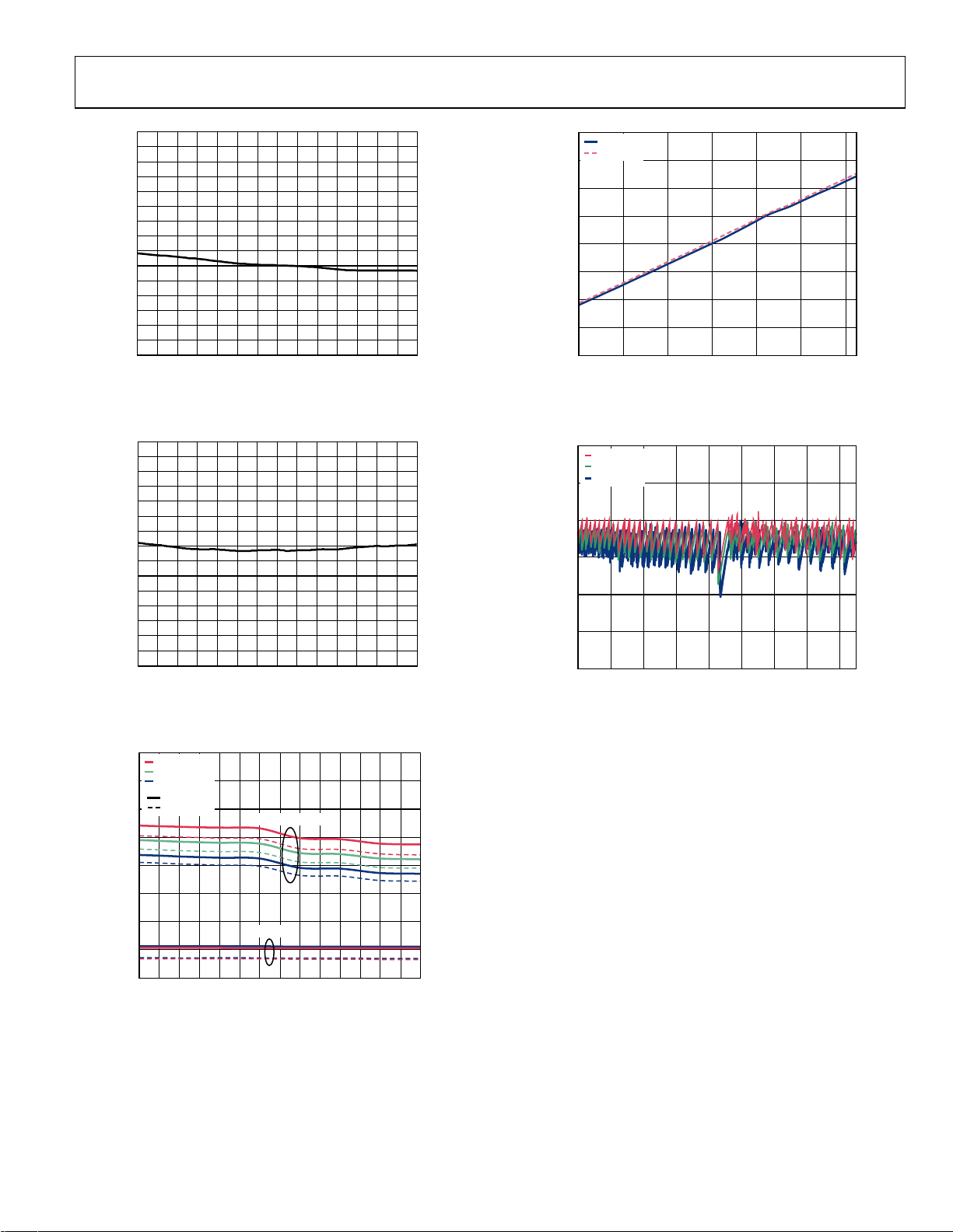
EVALUATION BOARD LAYOUT AND THERMAL GROUNDING
An evaluation board is available for testing the ADRF6807. The
evaluation board schematic is shown in Figure 43.
Tabl e 7 provides the component values and suggestions for
modifying the component values for the various modes of
operation.
09993-042
VOCM
IBBP
IOUT_ SE
R3
OPEN
R40
VCC
0Ω0Ω
VCC_BB
VCC_RF
R29 R32
VCC
C28
10µF
3P3V_FORCE
R31
0Ω
VCC_LO
R6
0Ω
S1
R56
10kΩ
R55
10kΩ
VCC
4
T2
3
R4
0Ω
0Ω
R45
VCC_LO
C7
0.1µF
C8
100pF
LO
9
R
5.6kΩ
0Ω
R38
CP
IBBN
R39
OPEN
0Ω
2
5
1
R5
0Ω
P2
R41
OPEN
0Ω
R46
2
T1
5
13
4
0Ω
R12
C13
62pF
R10
C15
1.6kΩ
6.2nF
OPEN
R11
C14
300pF
0Ω
R37
DECL3
C30
0.1µF
1nF
C6 C5
1nF
C1
100pF
OPEN
R1
C2
0.1µF
C35
10µF
R49
3P3V1
R13
OPEN
VCC3
VCC_RF
0.1µF
C25
VCC_RF
10µF
C36
0Ω
R28
100pF
C26
100pF
40 39 38 37 36 35 34 33 32 31
VCO_LDO
3P3V2
0Ω
C24
29
30
GND
GND
IBBN
IBBP
VCCLO
GND
LOSEL
LON
LOP
VTUNE
DECL1
VCC1
1
R7
R15
27
28
GND
DECL3
VCCRF
GND
VCC1
CPOUT
2
3
456
C12
100pF
0Ω
R8
C11
0.1µF
C3
10µF
C10
100pF
0Ω
C9
0.1µF
0Ω
C4
10µF
P1
3P3V_FORCE
R62
R63
4.99kΩ
RFIN
3
1
T4
4
6
VCC_BB1
R25
1000pF
1000pF
C38
26
RFIN
VOCM
C39
JP1
23
24
25
GND
RFIP
VOCM
ADRF6807
RSET
GND
REFIN
MUXOUT
789
R2
OPEN
1nF
C31
R16
R26
49.9Ω
REFIN
QBBP
4.99kΩ
R23
OPEN
R43
VCC_BB
0.1µF
0Ω
C22 C23
100pF
C40
0.1µF
22
21
GND
VCCBB
VCC2
DECL2
10
0Ω
REFOUT
T3
1
0Ω
R21
0Ω
R47
GND
QBBN
QBBP
VCCLO
GND
LE
GND
LE
CLK
DATA
12 13 14 15 16 17 18 19 20
GND
11
DATA
C16
100pF
0Ω
R18
C17
0.1µF
2P5V_LDO
C27
10µF
2P5V
QBBN
QOUT_SE
R42
OPEN
0Ω
245
R48
R51
C33
OPEN
OPEN
VCC2
OPEN
OPEN
C29
0.1µF
0Ω
R22
VCC_LO1
0Ω
VCC_LO
C20
0Ω
R24
C21
100pF
R57
0Ω
CLK
C18
100pF
0Ω
C19
0.1µF
0Ω
R27
3.3V_FORCE
3.3V_SENSE
C37
10µF
0Ω
R34
0.1µF
OPEN
R50
C32
OPEN
R14
CLK LE
DATA
DIG_GND
GND
GND1
VCC3
0Ω
GND2
LEGEND
NET NAME
TEST POINT
SMA INPUT/OUTPUT
3
P3
OPEN
R44
R52
C34
R17
Figure 43. Evaluation Board Schematic
Rev. B | Page 25 of 36
Page 26

ADRF6807 Data Sheet
CR1
R65
2kΩ
LE
CLK
DATA
3V3_USB
C58
0.1µF
R64
100kΩ
33
41
42
3V3_USB
R62
100kΩ
C45
0.1µF
47 46 45 44 43
48
3V3_USB
56 55 54 53 52 51 50 49
C51
22pF
1
2
Y1
24MHz
4
3
C54
22pF
VCC
GND
VCC
GND
RESET_N
WAKEUP
PD0_FD8
PD1_FD9
PD2_FD10
PD3_FD11
PD4_FD12
PD5_FD13
PD6_FD14
PD7_FD15
CLKOUT
RDY0_SLRD
1
GND
RDY1_SLWR
2
C48
10pF
38
39
40
PA7_FLAGD_SCLS_N
AVCC
3
37
PA6_PKTEND
PA5_FIFOARD1
PA4_FIFOARD0
XTALIN
XTALOUT
AGND
4
5
6
C49
0.1µF
36
PA3_WU2
CY7C68013A-56LTXC
AVCC
7
34
35
PA2_SLOE
PA1_INT1_N
PA0_INT0_N
U4
AGND11VCC12GND13IFCLK14RESERVED
DMINUS
DPLUS
8
9
10
R61
2kΩ
CR2
30
31
32
VCC
29
GND
CTL1_FLAGB
CTL2_FLAGC
28
CTL0_FLAGA
VCC
27
GND
26
PB7_FD7
25
PB6_FD6
24
PB5_FD5
23
PB4_FD4
3V3_USB
PB3_FD3
PB2_FD2
PB1_FD1
PB0_FD0
VCC
SDA
SCL
15 16 17 18 19 20 21 22
C56
10pF
R19
2kΩ
U2
24LC64-I_SN
5V_USB
C47
1.0µF
8
7
6
SD
IN2
IN1
U3
ADP3334
OUT1
OUT2
FB
1
2
3
3V3_USB
C57
0.1µF
R60
2kΩ
3V3_USB
5
6
7
SCL
SDA
A0
1
WC_N
A1
A2
2
3
R69
C50
1000pF
R70
140kΩ
C52
1.0µF
3V3_USB
8
VCC
GND
4
09993-144
DGND
5
GND
NC
4
78.7kΩ
5V_USB
12345
P5
3V3_USB
G1G2G3
3V3_USB
G4
Figure 44. Evaluation Board USB Section Schematic
Rev. B | Page 26 of 36
C46
0.1µF
C44
0.1µF
3V3_USB
C55
0.1µF
C53
0.1µF
C42
0.1µF
C41
0.1µF
C43
0.1µF
3V3_USB
Page 27

Data Sheet ADRF6807
The package for the ADRF6807 features an exposed paddle on
the underside that should be well soldered to an exposed opening
in the solder mask on the evaluation board. Figure 45 illustrates
the dimensions used in the layout of the ADRF6807 footprint on
the ADRF6807 evaluation board (1 mil = 0.0254 mm).
Note the use of nine via holes on the exposed paddle. These
ground vias should be connected to all other ground layers on
the evaluation board to maximize heat dissipation from the device
package. Under these conditions, the thermal impedance of the
ADRF6807 was measured to be approximately 30°C/W in still air.
0.012
0.050
0.025
0.020
Figure 45. Evaluation Board Layout Dimensions for the ADRF6807 Package
0.177
0.232
0.035
0.168
09993-044
Figure 46. ADRF6807 Evaluation Board Top Layer
09993-043
Figure 47. ADRF6807 Evaluation Board Bottom Layer
09993-045
Rev. B | Page 27 of 36
Page 28

ADRF6807 Data Sheet
Table 7. Evaluation Board Configuration Options
Component Function Default Condition
VCC, VCC2, VCC_LDO, VCC_LO,
VCC_LO1, VCC_RF, VCC_BB1, 3P3V1,
3P3V2, 3P3V_FORCE, 2P5V, CLK,
DATA, LE, CP, DIG_GND, GND, GND1,
GND2
R1, R6, R7, R8, R13, R14, R15, R17,
R18, R24, R25, R27, R28, R29, R31,
R32, R34, R36, R49
C1, C2, C3, C4, C7, C8, C9, C10, C11,
C12, C16, C17, C18, C19, C20, C21,
C22, C23, C24, C25, C26, C27, C28,
C35, C36, C37, C40
T1, C5, C6
R16, R26, R58, C31
R2, R9, R10, R11, R12, R37, R38, R59,
C14, C15, C13
R3, R4, R5, R21, R22, R23, R39, R40,
R41, R42, R43, R44, R45, R46, R47,
R48, C29, C30, T2, T3, P2, P3
C38, C39, T4
Power supply, ground and other test points.
Connect a 5 V supply to VCC. Connect a 3.3 V
supply to 3P3V_FORCE.
Power supply decoupling. Shorts or power supply
decoupling resistors.
The capacitors provide the required decoupling of
the supply-related pins.
External LO path. The T1 transformer provides
single-ended-to-differential conversion. C5 and C6
provide the necessary ac coupling.
REFIN input path. R26 provides a broadband 50 Ω
termination followed by C31, which provides the
ac coupling into REFIN. R16 provides an external
connectivity to the MUXOUT feature described in
Register 4. R58 provides option for connectivity to
the P1-6 line of a 9-pin D-sub connector for dc
measurements.
Loop filter component options. A variety of loop
filter topologies is supported using component
placements, C13, C14, C15, R9, and R10. R38 and
R59 provide connectivity options to numerous test
points for engineering evaluation purposes. R2
provides resistor programmability of the charge
pump current (see the Register 4—Charge Pump,
PFD, and Reference Path Control section). R37
connects the charge pump output to the loop filter.
R12 references the loop filter to the VCO_LDO.
IF I/Q output paths. The T2 and T3 baluns provide a
9:1 impedance transformation; therefore, with a 50 Ω
load on the single-ended IOUT/QOUT side, the center
tap side of the balun presents a differential 450 Ω
to the ADRF6807. The center taps of the baluns are
ac grounded through C29 and C30. The baluns create
a differential-to-single-ended conversion for ease
of testing and use, but an option to have straight
differential outputs is achieved by populating R3,
R39, R23, and R42 with 0 Ω resistors and removing
R4, R5, R21, and R22. P2 and P3 are differential
measurement test points (not to be used as jumpers).
RF input interface. T4 provides the single-endedto-differential conversion required to drive RFIP and
RFIN. T4 provides a 2:1 impedance transformation.
A single-ended 50 Ω load on the RFIN SMA
connector transforms to a differential 100 Ω
presented across the RFIP (Pin 25) and RFIN (Pin 26)
pins. C38 and C39 are ac coupling capacitors.
Rev. B | Page 28 of 36
VCC, VCC2, VCC_LO, VCC_RF, VCC_BB1,
VCC_LO1, VCO_LDO, 3P3V1, 3P3V2, 2P5V =
Components Corporation TP-104-01-02,
CP, LE, CLK, DATA, 3P3V_FORCE =
Components Corporation TP-104-01-06,
GND, GND1, GND2, DIG_GND =
Components Corporation TP-104-01-00
R1, R6, R7, R8 = 0 Ω (0402),
R13, R14, R15, R17 = 0 Ω (0402),
R18, R24, R25, R27 = 0 Ω (0402),
R28, R29, R31, R32 = 0 Ω (0402),
R34, R36 = 0 Ω (0402),
R49 = open (0402)
C1, C8, C10, C12 = 100 pF (0402),
C16, C18, C21, C22 = 100 pF (0402),
C24, C26 = 100 pF (0402),
C2, C7, C9, C11 = 0.1 μF (0402),
C17, C19, C20, C23 = 0.1 μF (0402),
C25, C40 = 0.1 μF (0402),
C3, C4, C27, C35 = 10 μF (0603),
C36, C37 = 10 μF (0603),
C28 = 10 μF (3216)
C5, C6 = 1 nF (0603),
T1 = TC1-1-13+ Mini-Circuits
R26 = 49.9 Ω (0402),
R16 = 0 Ω (0402),
R58 = open (0402),
C31 = 1 nF (0603)
R12, R37, R38 = 0 Ω (0402),
R59 = open (0402),
R9 = 5.6 kΩ (0402),
R10 = 1.6 kΩ (0402),
R2, R11 = open (0402),
C13 = 62 pF (0402),
C14 = 300 pF (0402),
C15 = 6.2 nF (1206)
R4, R5, R21, R22, = 0 Ω (0402),
R40, R43, R45, R46 = 0 Ω (0402),
R47, R48 = 0 Ω (0402),
R3, R23, R39, R41, R42, R44 = open (0402),
C29, C30, = 0.1 μF (0402),
T2, T3 = TCM9-1+ Mini-Circuits,
P2, P3 = Samtec SSW-102-01-G-S
C38, C39 = 1000 pF (0402),
T4 = ADTL2-18+ Mini-Circuits
Page 29

Data Sheet ADRF6807
Component Function Default Condition
R50, R51, R52, C32, C33, C34
R33, R55, R56, S1
J1, P1, R62, R63
U2, U3, U4, P5 Cypress microcontroller, EEPROM and LDO.
C41, C42, C43, C44, C46, C53, C55
C48, C49, C45, C56, C57, C58, R19,
R60, R61, R62, R64, CR2
C47, C50, C52, R65, R69, R70, CR1 LDO components.
Y1, C51, C54
Serial port interface. Optional RC filters can be
installed on the CLK, DATA, and LE lines to filter the
PC signals through R50 to R52 and C32 to C34. CLK,
DATA, and LE signals can be observed via test points
for debug purposes.
LO select interface. The LOSEL pin, in combination
with the LDRV and LXL bits in Register 5, controls
whether the LOP and LON pins operate as inputs or
outputs. A detailed description of how the LOSEL pin,
LDRV bit, and the LXL bit work together to control
the LOP and LON pins is found in Tabl e 4 under the
LOSEL pin description. Using the S1 switch, the
user can pull LOSEL to a logic high (V
low (ground). Resistors R55 and R56 form a resistor
divider to provide a logic high of VCC/2. LO select
can also be controlled through Pin 9 of J1. The 0 Ω
jumper, R33, must be installed to control LOSEL via J1.
Engineering test points and external control. J1 is a
10-pin connector connected to various important
points on the evaluation board that the user can
measure or force voltages upon. R62 and R63 form
a voltage divider to force a voltage of 1.65 V on
VOCM. Note that Jumper P5 must be connected to
drive VOCM with the resistor divider.
3.3 V supply decoupling. Several capacitors are
used for decoupling on the 3.3 V supply.
Cypress and EEPROM components.
Crystal oscillator and components. 24 MHz crystal
oscillator.
/2) or a logic
CC
R50, R51, R52 = open (0402),
C32, C33, C34 = open (0402)
R33 = 0 Ω (0402),
R55, R56 = 10 kΩ (0402),
S1 = Samtec TSW-103-08-G-S
R62 = R63 = 4.99 kΩ (0402),
P1 = Samtec SSW-102-01-G-S,
J1 = Molex Connector Corp. 10-89-7102
U2 = Microchip MICRO24LC64
U3 = Analog Devices ADP3334ACPZ
U4 = Cypress Semiconductor
CY7C68013A-56LTXC
P5 = Mini USB connector
C41, C42, C43, C44, C46, C53, C55 = 0.1 μF
(0402)
C48, C56 = 10 pF (0402)
C45, C49, C57, C58 = 0.1 μF (0402)
R19, R60, R61 = 2 kΩ (0402)
R62, R64 = 100 kΩ (0402)
CR2 = ROHM SML-21OMTT86
C47, C52 = 1 μF (0402)
C50 = 1000 pF (0402)
R65 = 2 kΩ (0402)
R69 = 78.7 kΩ (0402)
R70 = 140 kΩ (0402)
CR1 = ROHM SML-21OMTT86
Y1 = NDK NX3225SA-24 MHz
C51, C54 = 22 pF (0402)
Rev. B | Page 29 of 36
Page 30

ADRF6807 Data Sheet
ADRF6807 SOFTWARE
The ADRF6807 evaluation board can be controlled from PCs
using a USB adapter board, which is also available from Analog
Devices, Inc. The USB adapter evaluation documentation and
ordering information can be found on the EVAL-ADF4XXXZ-USB
product page. The basic user interfaces are shown in Figure 48 and
Figure 49.
The software allows the user to configure the ADRF6807 for
various modes of operation. The internal synthesizer is controlled
by clicking any of the numeric values listed in RF Section.
Attempting to program Ref Input Frequency, PFD Frequency,
VCO Frequency (2×LO), LO Frequency, or other values in RF
Section launches the Synth Form window shown in Figure 49.
Usi ng Synth Form, the user can specify values for Local Oscillator
Frequency (MHz) and External Reference Frequency (MHz).
The user can also enable the LO output buffer and divider options
from this menu. After setting the desired values, it is important
to click Upload all registers for the new setting to take effect.
9993-148
Figure 48. Evaluation Board Software Main Window
Rev. B | Page 30 of 36
Page 31

Data Sheet ADRF6807
09993-149
Figure 49. Evaluation Board Software Synth Form Window
Rev. B | Page 31 of 36
Page 32

ADRF6807 Data Sheet
CHARACTERIZATION SETUPS
Figure 50 to Figure 52 show the general characterization bench
setups used extensively for the ADRF6807. The setup shown in
Figure 50 was used to perform the bulk of the testing. An automated
Agilent VEE program was used to control the equipment over the
IEEE bus. This setup was used to measure gain, input P1dB, output
P1dB, input IP2, input IP3, IQ gain mismatch, IQ quadrature
accuracy, and supply current. The evaluation board was used to
perform the characterization with a Mini-Circuits TCM9-1+ balun
on each of the I and Q outputs. When using the TCM9-1+ balun
below 5 MHz (the specified 1 dB low frequency corner of the
balun), distortion performance degrades; however, this is not
the ADRF6807 degrading, merely the low frequency corner of
the balun introducing distortion effects. Through this balun, the
9-to-1 impedance transformation effectively presented a 450 Ω
differential load at each of the I and Q channels. The use of the
broadband Mini-Circuits ADTL2-18+ balun on the input
provided a differential balanced RF input. The losses of both
the input and output baluns were de-embedded from all
measurements.
To perform phase noise and reference spur measurements, the
setup shown in Figure 52 was used. Phase noise was measured
at the baseband output (I or Q) at a baseband carrier frequency
of 50 MHz. The baseband carrier of 50 MHz was chosen to allow
phase noise measurements to be taken at frequencies of up to
20 MHz offset from the carrier. The noise figure was measured
using the setup shown in Figure 51 at a baseband frequency
of 10 MHz.
Rev. B | Page 32 of 36
Page 33

Data Sheet ADRF6807
IEEE
R&S SMA100
SIGNAL G ENERATOR
IEEE
IEEE
IEEE
IEEE
R&S SMT03 SIGNAL GENERAT OR
R&S SMT03 SIGNAL GENERAT OR
IEEE
AGILENT MXA
SPECTRUM ANALYZER
IEE E
IEEE
(FOR I-5V VP1 MEAS.)
AGILENT E3631A
POWER SUPPLY
IEEE
IE
(USED AS COMBINER)
AGILENT DMM
AGILENT DMM
(FOR I 3.3V VP2 MEAS.)
RF1
AGILENT 11636A
POWER DIV IDER
RF2
HP 8508A
VECTOR
VOLTMETER
AGILENT 34980A
MULTIF UNCTION
SWITCH
(WITH 34950 AND 2×
34921 MODULES)
3dB
3dB
CH A
CH B
10-PIN
CONNECTIO N
(+5V VPOS1,
+3.3V VPOS2,
DC MEASURE)
9-PIN D-SUB CONNE CTION
(VCO AND PLL PROGRAMMING)
IEEE
IEEE
3dB
MINI CIRCUI TS
ZHL-42W AMPLIFIER
(SUPPLIED WITH +15VDC
FOR OPERAT ION)
3dB
RF
RF SWIT CH MATRIX
I CH
6dB 3dB
RF
ADRF6807
EVALUATIO N BOARD
6dB
REF
REF
Q CH
6dB
IEEE
Figure 50. General Characterization Setup
Rev. B | Page 33 of 36
IEEE
09993-048
Page 34

ADRF6807 Data Sheet
IEEE
AGILENT 8665B
LOW NOISE SYN
SIGNAL GENERATOR
REF
RF1
IEEE
IEEE
E
IEEE
AGILENT E3631A
POWER SUPPLY
IEEE
IE
AGILENT 346B
NOISESO URCE
AGILENT N8974A
NOISE FI GURE ANALYZER
AGILENT DMM
(FOR I-5V VP1 MEAS.)
AGILENT DMM
(FOR I 3.3V VP2 MEAS .)
10MHz
LOW-PASS FILTER
AGILENT 34980A
MULTIFUNCTION
SWITCH
(WITH 34950 AND 2×
34921 MODULES)
IEEE
IEEE
I CH
6dB 3dB 6dB
10-PIN
CONNECTIO N
(+5V VPOS1,
+3.3V VPOS2,
DC MEASURE)
9-PIN D-SUB CONNE CTION
(VCO AND PLL PROGRAMMING)
3dB
RF
RF SWITCH MATRIX
RF
ADRF6807
EVALUATIO N BOARD
6dB
REF
Q CH
IEEE
Figure 51. Noise Figure Characterization Setup
Rev. B | Page 34 of 36
IEEE
09993-049
Page 35

Data Sheet ADRF6807
IEEE
R&S SMA100
SIGNAL GE NERATOR
IEEE
IEEE
IEEE
IEEE
AGILENT E5052 SIGNAL SOURCE
E
IEEE
AGILENT E3631A
POWER SUPPLY
IEEE
IE
R&S SMA100
SIGNAL G ENERATOR
ANALYZER
AGILENT MXA
SPECTRUM ANALYZ ER
AGILENT DMM
(FOR I -5V VP1 MEAS. )
AGILENT DMM
(FOR I 3.3V VP2 MEAS.)
100MHz
LOW-PASS FILTER
AGILENT 34980A
MULTIFUNCTION
SWITCH
(WITH 34950 AND 2×
34921 MODULES)
IEEE
IEEE
RF1
I CH
6dB 3dB 6dB
10-PIN
CONNECTION
(+5V VPO S1,
+3.3V VPOS2,
DC MEASURE)
9-PIN D-SUB CONNE CTION
(VCO AND PLL PROGRAMMING )
3dB
RF
RF SWITCH MATRIX
RF
ADRF6807
EVALUATIO N BOARD
6dB
REF
REF
Q CH
IEEE
IEEE
09993-050
Figure 52. Phase Noise Characterization Setup
Rev. B | Page 35 of 36
Page 36

ADRF6807 Data Sheet
S
OUTLINE DIMENSIONS
6.00
INDICATOR
1.00
0.85
0.80
EATING
PLANE
PIN 1
12° MAX
BSC SQ
TOP
VIEW
0.80 MAX
0.65 TYP
0.30
0.23
0.18
COMPLI ANT TO JEDEC STANDARDS MO -220-VJJD-2
5.75
BSC SQ
0.20 REF
0.05 MAX
0.02 NOM
COPLANARIT Y
0.60 MAX
0.50
BSC
0.50
0.40
0.30
0.08
Figure 53. 40-Lead Lead Frame Chip Scale Package [LFCSP_VQ]
6 mm × 6 mm Body, Very Thin Quad
(CP-40-4)
Dimensions shown in millimeters
0.60 MAX
29
28
EXPOSED
(BOTTOM VIEW)
20
19
40
1
PAD
10
11
4.50
REF
FOR PROP ER CONNECTIO N OF
THE EXPOSED PAD, REFER TO
THE PIN CO NFIGURAT ION AND
FUNCTIO N DESCRIPTIONS
SECTION OF THIS DATA SHEET.
PIN 1
INDICATOR
4.45
4.30 SQ
4.15
0.25 MIN
122107-A
ORDERING GUIDE
Ordering
Model1 Temperature Range Package Description Package Option
ADRF6807ACPZ-R7 −40°C to +85°C 40-Lead Lead Frame Chip Scale Package [LFCSP_VQ] CP-40-4 750
ADRF6807-EVALZ Evaluation Board
1
Z = RoHS Compliant Part.
Quantity
©2011–2012 Analog Devices, Inc. All rights reserved. Trademarks and
registered trademarks are the property of their respective owners.
D09993-0-2/12(B)
Rev. B | Page 36 of 36
 Loading...