

Page 1
with Integrated Fractional
-
N PLL and VC
O
ADRF6755
V
Preliminary Technical Data
FEATURES
I/Q modulator with integrated fractional-N PLL and VCO
Gain control span: 47 dB in 1 dB steps
Output frequency range: 300 MHz to 2310 MHz
Output 1 dB compression: 8 dBm
Output IP3: 21 dBm
Noise floor: −162 dBm/Hz
Baseband modulation bandwidth: 600 MHz (3 dB)
Output frequency resolution: 1 Hz
SPI and I2C-compatible serial interfaces
Power supply: 5 V/350 mA
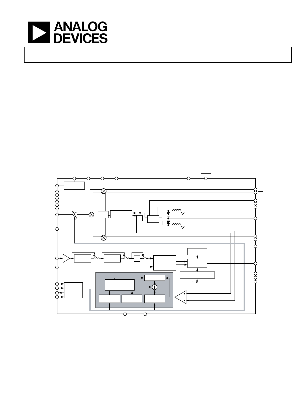
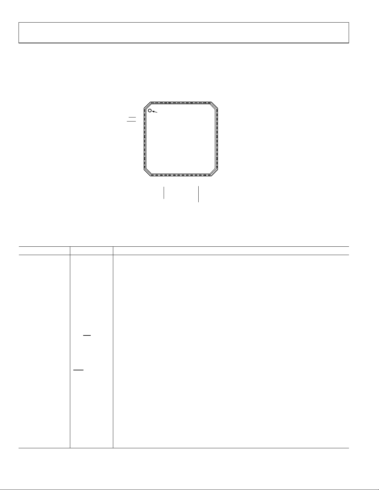
FUNCTIONAL BLOCKDIAGRAM
CC1VCC2VCC3VCC4
300 MHz to 2310 MHz I/Q Modulator
GENERAL DESCRIPTION
The ADRF6755 is a highly integrated quadrature modulator,
frequency synthesizer, and programmable attenuator. The
device covers an operating frequency range from 300 MHz
to 2310 MHz for use in satellite, cellular and broadband
communications.
The ADRF6755 modulator includes a high modulus fractional-N
frequency synthesizer with integrated VCO, providing better
than 1 Hz frequency resolution, and a 47 dB digitally controlled
output attenuator with 1 dB steps.
Control of all the on-chip registers is through a user-selected
SPI interface or I2C interface. The device operates from a single
power supply ranging from 4.75 V to 5.25 V.
LOMON
LOMON
REGOUT
VREG1
VREG2
VREG3
VREG4
VREG5
VREG6
RFOUT
TXDIS
REFIN
REFIN
SDI/SDA
CLK/SCL
SDO
CS
3.3V
REGULATOR
47dB
GAIN CONTROL
RANGE
×2
DOUBLER
SPI/
I2C
INTERFACE
ADRF6755
RFDIVIDER
0°/90°
5-BIT
DIVIDER
THIRD-ORDER
FRACTIONAL
INTERPOLATOR
FRACTIONAL
REGISTER
÷2
MODULUS
25
2
AGND DGND
VCO
CORE
+
FREQUENCY
DETECTOR
–
N-COUNTER
INTEGER
REGISTER
Figure 1.
PHASE
REFERENCE
CHARGE
PUMP
CURRENT SETTING
CR9[7:4]
IBB
IBB
CCOMP1
CCOMP2
CCOMP3
VTUNE
QBB
QBB
RSET
CP
LF3
LF2
LDET
08201-001
Rev. PrD
Information furnished by Analog Devices is believed to be accurate and reliable. However, no
responsibility is assumed by Analog Devices for its use, nor for any infringements of patents or other
rights of third parties that may result from its use. Specifications subject to change without notice. No
license is granted by implication or otherwise under any patent or patent rights of Analog Devices.
Trademarks and registered trademarks are the property of their respective owners.
One Technology Way, P.O. Box 9106, Norwood, MA 02062-9106, U.S.A.
Tel: 781.329.4700 www.analog.com
Fax: 781.461.3113 ©2012 Analog Devices, Inc. All rights reserved.
Page 2

ADRF6755
TABLE OF CONTENTS
Features .............................................................................................. 1
General Description ......................................................................... 1
Functional Block Diagram .............................................................. 1
Specifications ..................................................................................... 3
Timing Characteristics ................................................................ 5
Absolute Maximum Ratings ............................................................ 7
ESD Caution .................................................................................. 7
Pin Configuration and Function Descriptions ............................. 8
Typical Performance Characteristics ........................................... 10
Theory of Operation ...................................................................... 18
Overview...................................................................................... 18
Preliminary Technical Data
SPI Interface ................................................................................ 24
Program Modes .......................................................................... 26
Register Map ................................................................................... 28
Register Map Summary ............................................................. 28
Register Bit Descriptions ........................................................... 29
Suggested Power-Up Sequence ..................................................... 33
Initial Register Write Sequence ................................................ 33
Evaluation Board ............................................................................ 35
General Description ................................................................... 35
Hardware Description ............................................................... 35
PCB Artwork .............................................................................. 38
PLL Synthesizer and VCO ......................................................... 18
Quadrature Modulator .............................................................. 21
Attenuator .................................................................................... 22
Voltage Regulator ....................................................................... 22
I2C Interface ................................................................................ 22
Bill of Materials........................................................................... 41
Outline Dimensions ....................................................................... 42
Ordering Guide .......................................................................... 42
Rev. PrD | Page 2 of 43
Page 3

Preliminary Technical Data ADRF6755
SPECIFICATIONS
VCC = 5 V, TA = 25°C, I/Q inputs = 0.9 V p-p differential sine waves in quadrature on a 500 mV dc bias, REFIN = 80 MHz, PFD = 40 MHz,
baseband frequency = 1 MHz, LOMON off, unless otherwise noted.
Table 1.
Parameter Test Conditions/Comments Min Typ Max Unit
RF OUTPUT RFOUT pin
Operating Frequency Range 300 2310 MHz
Nominal Output Power VIQ = 0.9 V p-p differential −0.5 dBm
Gain Flatness Any 40 MHz ±0.1 dB
Output P1dB 8 dBm
Output IP3 f1BB = 3.5 MHz, f2BB = 4.5 MHz, P
Output Return Loss Attenuator setting = 0 dB −15 dB
LO Carrier Feedthrough Attenuator setting = 0 dB to 47 dB −45 dBc
2× LO Carrier Feedthrough Attenuator setting = 0 dB to 47 dB −45 dBm
Sideband Suppression −45 dBc
Noise Floor I/Q inputs = 0 V p-p differential, Attenuator setting = 0 dB −162 dBm/Hz
Attenuator setting = 0 dB to 21 dB, carrier offset = 15 MHz −147 dBc/Hz
Attenuator setting = 21 dB to 47 dB, carrier offset = 15 MHz −170 dBm/Hz
Harmonics −55 dBc
REFERENCE CHARACTERISTICS REFIN pin
Input Frequency With R divide-by-2 enabled 10 300 MHz
With R divide-by-2 disabled 10 165 MHz
Input Sensitivity AC-coupled 0.4 VREG V p-p
Input Capacitance 10 pF
Input Current ±100 µA
CHARGE PUMP
ICP Sink/Source Programmable, RSET = 4.7 kΩ
High Value 5 mA
Low Value 312.5 µA
Absolute Accuracy 4.0 %
VCO
Gain K
SYNTHESIZER SPECIFICATIONS
Frequency Resolution 1 Hz
Spurs Integer boundary < loop bandwidth −55 dBc
> 256 kHz offset from carrier −65 dBc
>10 MHz offset from carrier −75 dBc
Phase Noise1 LO = 2310 MHz
100 Hz offset −85 dBc/Hz
1 kHz offset −96 dBc/Hz
10 kHz offset −100 dBc/Hz
100 kHz offset −106 dBc/Hz
1 MHz offset −132 dBc/Hz
>15 MHz offset −152 dBc/Hz
Integrated Phase Noise1 1 kHz to 8 MHz integration bandwidth, LO=2310MHz 0.20
Frequency Settling1 Any step size, maximum frequency error = 100 Hz 0.17 ms
Maximum Frequency Step for
No Autocalibration
Phase Detector Frequency 10 40 MHz
25 MHz/V
VCO
Frequency step with no autocalibration routine;
Register CR24, Bit 0 = 1
= −6 dBm per tone 21 dBm
OUT
100/2
RFDIV
kHz
rms
Rev. PrD | Page 3 of 43
Page 4

ADRF6755
INH
INH
INL
Preliminary Technical Data
Parameter Test Conditions/Comments Min Typ Max Unit
GAIN CONTROL
Gain Range 47 dB
Step Size 1 dB
Relative Step Accuracy Fixed frequency, adjacent steps
All attenuation steps ±0.3 dB
Over full frequency range, adjacent steps ±1.5 dB
Absolute Step Accuracy2 47 dB attenuation step −2.0 dB
Output Settling Time Any step; output power settled to ±0.2 dB 15 µs
OUTPUT DISABLE TXDIS pin
Off Isolation RFOUT, Attenuator setting = 0 dB to 47 dB, TXDIS high −100 dBm
LO, Attenuator setting = 0 dB to 47 dB, TXDIS high −80 dBm
2 x LO, Attenuator setting = 0 dB to 47 dB, TXDIS high −50 dBm
Turn-On Settling Time TXDIS high to low: Output power to 90% of envelope 500 ns
Frequency settling to 100Hz 2 µs
Turn-Off Settling Time TXDIS low to high (to −55 dBm) 500 ns
MONITOR OUTPUT
LOMON,
LOMON
pins,
Nominal Output Power −24 dBm
BASEBAND INPUTS
IBB
, QBB,
QBB
pins
IBB,
I and Q Input Bias Level 500 mV
3 dB Bandwidth 600 MHz
LOGIC INPUTS
Input High Voltage, V
Input Low Voltage, V
Input High Voltage, V
Input Low Voltage, V
Input Current, I
INH/IINL
CS, TXDIS pins 1.4 V
CS, TXDIS pins 0.6 V
INL
SDI/SDA, CLK/SCL pins 2.1 V
SDI/SDA, CLK/SCL pins 1.1 V
CS, TXDIS, SDI/SDA, CLK/SCL pins ±1 µA
Input Capacitance, CIN CS, TXDIS, SDI/SDA, CLK/SCL pins 10 pF
LOGIC OUTPUTS
Output High Voltage, VOH SDO, LDET pins; IOH = 500 µA 2.8 V
Output Low Voltage, VOL SDO, LDET pins; IOL = 500 µA 0.4 V
SDA (SDI/SDA); IOL = 3 mA 0.4 V
POWER SUPPLIES VCC1, VCC2, VCC3, VCC4, VREG1, VREG2, VREG3, VREG4,
VREG5, VREG6, and REGOUT pins
REGOUT normally connected to VREG1, VREG2, VREG3,
VREG4, VREG5, and VREG6
Voltage Range VCC1, VCC2, VCC3, and VCC4 4.75 5 5.25 V
REGOUT, VREG1, VREG2, VREG3, VREG4, VREG5, and
3.3 V
VREG6
Supply Current VCC1, VCC2, VCC3, and VCC4 combined; REGOUT con-
350 390 mA
nected to VREG1, VREG2, VREG3, VREG4, VREG5, and VREG6
Power Down Current CR29[0]=0, Power Down Modulator
7 mA
CR12[2]=1, Power Down PLL
CR28[4]=1, Power Down RFDIVIDER
CR27[2]=0, Power Down LOMON
Operating Temperature −40 85 °C
1
LBW = 100 kHz at LO = 2310 MHz; ICP = 5 mA.
2
All other attenuation steps have an absolute error of <±2.0 dB.
Rev. PrD | Page 4 of 43
Page 5
Preliminary Technical Data ADRF6755
SC
L
LOW
HD;STA
SU;DAT
SU;
STO
VD;DAT
BUF
08201-003
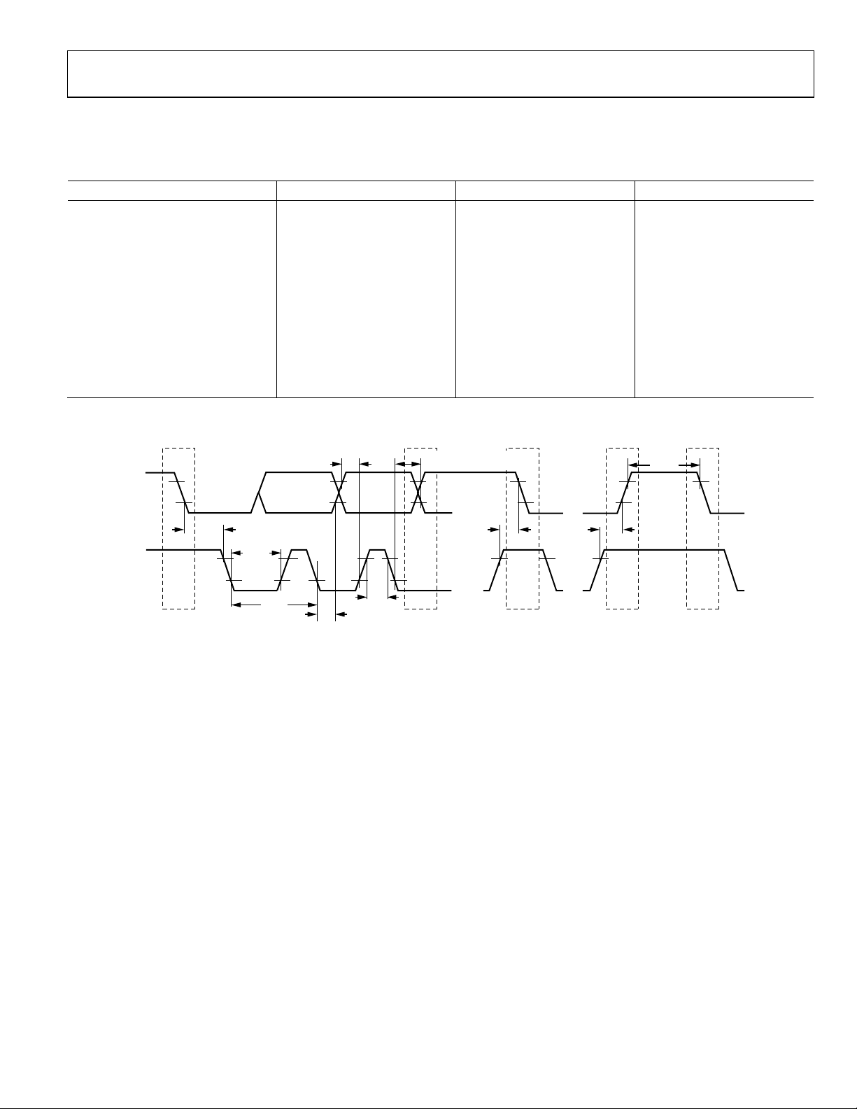
TIMING CHARACTERISTICS
I2C Interface Timing
Table 2.
Parameter1 Symbol Limit Unit
SCL Clock Frequency f
SCL Pulse Width High t
SCL Pulse Width Low t
Start Condition Hold Time t
Start Condition Setup Time t
Data Setup Time t
Data Hold Time t
Stop Condition Setup Time t
Data Valid Time t
Data Valid Acknowledge Time t
Bus Free Time t
1
See Figure 2.
400 kHz max
600 ns min
HIGH
1300 ns min
600 ns min
600 ns min
SU;STA
100 ns min
300 ns min
HD;DAT
600 ns min
900 ns max
900 ns max
VD;ACK
1300 ns min
t
t
SU;DAT
VD;DAT AND
t
VD;ACK (ACK SIGNAL ONLY)
t
BUF
SDA
SCL
t
HD;STA
t
LOW
S S SP
START
CONDITION
1/f
SCL
t
HD;DAT
t
HIGH
t
SU;STA
t
SU;STO
Figure 2. I2C Port Timing Diagram
STOP
CONDITION
Rev. PrD | Page 5 of 43
Page 6
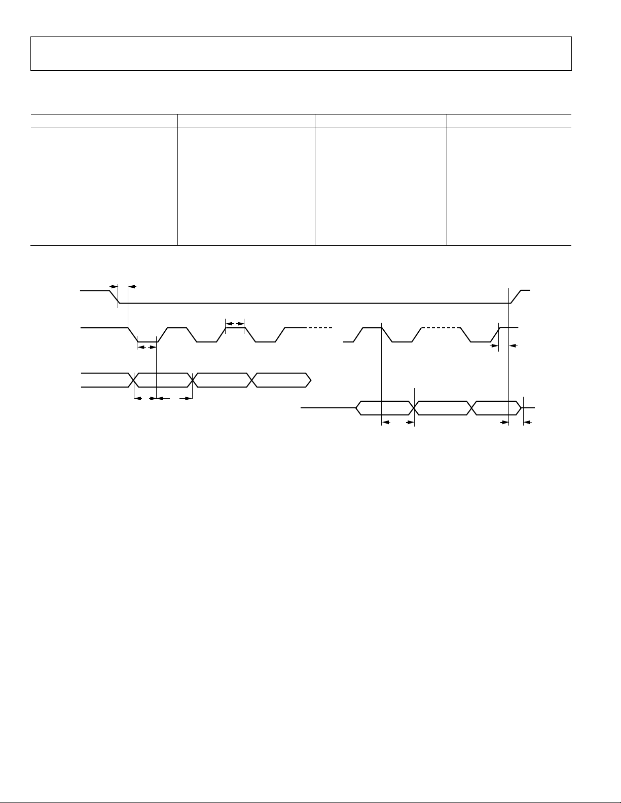
ADRF6755
t
Preliminary Technical Data
SPI Interface Timing
Table 3.
Parameter1 Symbol Limit Unit
CLK Frequency f
20 MHz max
CLK
CLK Pulse Width High t1 15 ns min
CLK Pulse Width Low t2 15 ns min
Start Condition Hold Time t3 5 ns min
Data Setup Time t4 10 ns min
Data Hold Time t5 5 ns min
Stop Condition Setup Time t6 5 ns min
SDO Access Time t7 15 ns min
CS to SDO High Impedance t8 25 ns max
1
See Figure 3.
3
CS
t
1
CLK
SDI
t
t
2
t
t
5
4
Figure 3. SPI Port Timing Diagram
SDO
t
7
6
t
8
08201-004
Rev. PrD | Page 6 of 43
Page 7
Preliminary Technical Data ADRF6755
ABSOLUTE MAXIMUM RATINGS
Table 4.
Parameter Rating
Supply Voltage VCC1, VCC2, VCC3, and VCC4 −0.3 V to +6 V
Supply Voltage VREG1, VREG2, VREG3, VREG4,
VREG5, and VREG6
IBB,
, QBB, and
IBB
Digital I/O −0.3 V to +4 V
Analog I/O (Other Than IBB,
)
QBB
Maximum Junction Temperature 125°C
Storage Temperature Range −65°C to +150°C
QBB
, QBB, and
IBB
−0.3 V to +4 V
0 V to 2.5 V
−0.3 V to +4 V
Stresses above those listed under Absolute Maximum Ratings
may cause permanent damage to the device. This is a stress
rating only; functional operation of the device at these or any
other conditions above those indicated in the operational
section of this specification is not implied. Exposure to absolute
maximum rating conditions for extended periods may affect
device reliability.
ESD CAUTION
Rev. PrD | Page 7 of 43
Page 8
Preliminary Technical Data ADRF6755
SET
T
PIN CONFIGURATION AND FUNCTION DESCRIPTIONS
D
2
2
N
N
C
C
G
G
C
C
A
A
V
V
3
4
5
6
5
5
5
5
PIN 1
1VCC4
INDICATOR
2IBB
3IBB
4QBB
5QBB
6AGND
7RSET
8LF3
9CP
10LF2
11VCC1
12REGOUT
13VREG1
14VREG2
NOTES
1. CONNECT EXPOSED PAD TO GROUND PLANE VIA
A LOW IMPEDANCE PATH.
6
7
5
1
1
1
3
4
N
I
G
G
F
E
E
E
R
R
R
V
V
ADRF6755
TOP VIEW
(Not to Scale)
8
1
N
I
F
E
R
U
N
N
N
N
O
F
G
G
G
G
R
A
A
A
A
2
8
9
0
1
5
4
4
5
5
1
9
0
2
1
2
22232
D
D
D
D
D
N
N
N
N
N
G
G
G
G
G
A
A
A
A
A
T
D
D
D
D
D
U
S
D
D
O
I
T
X
N
N
E
D
U
G
G
X
D
T
A
A
L
M
4
3
5
6
7
4
4
4
4
4
42 VCC3
41 VCC3
40 AGND
39 AGND
38 VTUNE
37 AGND
36 VREG6
35 CCOMP3
34 CCOMP2
33 CCOMP1
32 DGND
31 VREG5
30 CLK/SCL
29 SDI/SDA
4
5
6
7
8
2
2
2
2
S
D
N
N
O
C
N
O
D
O
S
G
M
M
A
O
O
L
L
08298-005
Figure 4. Pin Configuration
Table 5. Pin Function Descriptions
Pin No. Mnemonic Description
11, 55, 56, 41, 42, 1 VCC1 to VCC4 Positive Power Supplies for I/Q Modulator. Apply a 5 V power supply to VCC1, which should be
decoupled with power supply decoupling capacitors. Connect VCC2, VCC3, and VCC4 to the same
5 V power supply.
12 REGOUT 3.3 V Output Supply. Drives VREG1, VREG2, VREG3, VREG4, VREG5, and VREG6.
13, 14, 15, 16, 31,
36
6, 19, 20, 21, 22, 23,
VREG1 to
VREG6
Positive Power Supplies for PLL Synthesizer, VCO, and Serial Port. Connect these pins to REGOUT
(3.3 V) and decouple them separately.
AGND Analog Ground. Connect to a low impedance ground plane.
24, 37, 39, 40, 46,
47, 49, 50, 51, 52,
53, 54
32 DGND Digital Ground. Connect to the same low impedance ground plane as the AGND pins.
IBB,
2, 3
IBB
Differential In-Phase Baseband Inputs. These high impedance inputs must be dc-biased to approximately 500 mV dc and should be driven from a low impedance source. Nominal characterized ac
signal swing is 450 mV p-p on each pin. This results in a differential drive of 0.9 V p-p with a 500 mV
dc bias, resulting in a single sideband output power of approximately −1.6 dBm. These inputs are
not self-biased and must be externally biased.
4, 5
QBB
, QBB
Differential Quadrature Baseband Inputs. These high impedance inputs must be dc-biased to
approximately 500 mV dc and should be driven from a low impedance source. Nominal characterized ac signal swing is 450 mV p-p on each pin. This results in a differential drive of 0.9 V p-p with
a 500 mV dc bias, resulting in a single sideband output power of approximately −1.6 dBm. These
inputs are not self-biased and must be externally biased.
33, 34, 35 CCOMP1 to
Internal Compensation Nodes. These pins must be decoupled to ground with a 100 nF capacitor.
CCOMP3
38 VTUNE Control Input to the VCO. This voltage determines the output frequency and is derived from
filtering the CP output voltage.
7 RSET Charge Pump Current Set. Connecting a resistor between this pin and ground sets the maximum
charge pump output current. The relationship between ICP and R
is as follows:
Rev. PrD | Page 8 of 43
Page 9

Preliminary Technical Data ADRF6755
SET
CP max
Pin No. Mnemonic Description
5.23
I
CPmax
where R
9 CP Charge Pump Output. When enabled, this output provides ±ICP to the external loop filter, which, in
turn, drives the internal VCO.
27 CS Chip Select, CMOS Input. When CS is high, the data stored in the shift registers is loaded into one of
31 latches. In I2C mode, when CS is high, the slave address of the device is 0x60, and when CS is low,
the slave address is 0x40.
29 SDI/SDA Serial Data Input for SPI Port/Serial Data Input/Output for I2C Port. In SPI mode, this pin is a high
impedance CMOS data input, and data is loaded in an 8-bit word. In I2C mode, this pin is a bidirectional port.
30 CLK/SCL Serial Clock Input for SPI/I2C Port. This serial clock is used to clock in the serial data to the registers.
This input is a high impedance CMOS input.
28 SDO Serial Data Output for SPI Port. Register states can be read back on the SDO data output line.
17 REFIN Reference Input. This high impedance CMOS input should be ac-coupled.
18
REFIN
Reference Input Bar. This pin should be either grounded or ac-coupled to ground.
48 RFOUT RF Output. Single-ended, 50 Ω, internally biased RF output. This pin must be ac-coupled to the
load. Nominal output power is −1.6 dBm for a single sideband baseband drive of 0.9 V p-p differ-
ential on the I and Q inputs (attenuation = minimum).
45 TXDIS Output Disable. This pin can be used to disable the RF output. Connect to high logic level to disable
the output. Connect to low logic level for normal operation.
25, 26 LOMON,
LOMON
Differential Monitor Outputs. These pins provide a replica of the internal local oscillator frequency
(1× LO) at four different power levels: −6 dBm, −12 dBm, −18 dBm, and −24 dBm, approximately.
These open-collector outputs must be terminated with external resistors to REGOUT. These outputs
can be disabled through serial port programming and should be tied to REGOUT if not used.
10, 8 LF2, LF3 No connect pins.
44 LDET Lock Detect. This output pin indicates the state of the PLL: a high level indicates a locked condition,
whereas a low level indicates a loss of lock condition.
43 MUXOUT Muxout. This output is a test output for diagnostic use only. It should be left unconnected by the
customer.
Exposed Paddle EP Exposed Paddle. Connect to ground plane via a low impedance path.
R
SET
= 4.7 kΩ and I
= 5 mA.
Rev. PrD | Page 9 of 43
Page 10
Preliminary Technical Data ADRF6755
odata
vailabl
e
odatavailable
odatavailable
odatavailableodatavailabl
e
odatavailable
TYPICAL PERFORMANCE CHARACTERISTICS
VCC = 5 V, TA = 25°C, I/Q inputs = 0.9 V p-p differential sine waves in quadrature on a 500 mV dc bias, REFIN = 80 MHz, PFD = 40 MHz,
baseband frequency = 1 MHz, LOMON is off, unless otherwise noted. A nominal condition is defined as 25°C, 5.00 V, and worst-case
frequency. A worst-case condition is defined as having the worst-case temperature, supply voltage, and frequency.
Figure 5. Output Power vs. LO Frequency, Supply, and Temperature
Figure 6. Output Power Distribution at Nominal and
Worst-Case Conditions
Figure 8. Sideband Suppression vs. LO Frequency, Supply, and Temperature
Figure 9. Sideband Suppression Distribution at Nominal and
Worst-Case Conditions
Figure 7. Output Power vs. LO Frequency for External VCO Mode
at Nominal Conditions
Figure 10. LO Carrier Feedthrough vs. Attenuation, LO Frequency,
Supply, and Temperature
Rev. PrD | Page 10 of 43
Page 11
Preliminary Technical Data ADRF6755
odatavailable
odata
vailabl
e
odata
vailabl
e
odata
vailabl
e
odatavailable
odata
vailabl
e
Figure 11. LO Carrier Feedthrough Distribution at Nominal and Worst-Case
Conditions and Attenuation Setting
Figure 12. 2 × LO Carrier Feedthrough vs. Attenuation, LO Frequency,
Supply, and Temperature
Figure 14. Output P1dB Compression Point Distribution at Nominal
and Worst-Case Conditions
Figure 15. Output P1dB Compression Point vs. LO Frequency at
Nominal Conditions
Figure 13. Output P1dB Compression Point at Worst-Case LO Frequency
vs. Supply and Temperature
Rev. PrD | Page 11 of 43
Figure 16. Output IP3 Distribution at Nominal and Worst-Case
Conditions
Page 12
ADRF6755
odatavailable
odatavailable
odata
vailabl
e
odata
vailabl
e
odatavailable
odata
vailabl
e
Preliminary Technical Data
Figure 17. Output IP3 vs. LO Frequency at Nominal Conditions
Figure 18. LO Off Isolation vs. Attenuation, LO Frequency, Supply,
and Temperature
Figure 20. Second-Order and Third-Order Harmonic Distortion vs.
Figure 21. Noise Floor at 15 MHz Offset Frequency Distribution at
LO Frequency, Supply, and Temperature
Worst-Case Conditions and Different Attenuation Settings
Figure 19. 2 × LO Off Isolation vs. Attenuation, LO Frequency, Supply,
and Temperature
Figure 22. Noise Floor at 0 dB Attenuation vs. Output Power
at Nominal Conditions
Rev. PrD | Page 12 of 43
Page 13
Preliminary Technical Data ADRF6755
odata
vailabl
e
odata
vailabl
e
odata
vailabl
e
odatavailable
odatavailable
odata
vailabl
e
Figure 23. Normalized I and Q Input Bandwidth
Figure 24. Output Return Loss at Worst-Case Attenuation vs.
LO Frequency, Supply, and Temperature
Figure 26. RF Output Spectral Plot over a 100 MHz Span
Figure 27. RF Output Spectral Plot over a Wide Span
Figure 25. RF Output Spectral Plot over a 10 MHz Span
Rev. PrD | Page 13 of 43
Figure 28. Phase Noise Performance vs. LO Frequency, Supply,
and Temperature
Page 14

ADRF6755
odata
vailabl
e
odatavailable
odatavailable
odata
vailabl
e
odatavailableodatavailabl
e
Preliminary Technical Data
Figure 29. Phase Noise Performance Distribution at Worst-Case Conditions
Figure 30. Integer Boundary Spur Performance vs. LO Frequency,
Supply, and Temperature
Figure 32. Spurs > 10 MHz from Carrier vs. LO Frequency,
Supply, and Temperature
Figure 33. Integrated Phase Noise vs. LO Frequency at
Nominal Conditions
Figure 31. Integer Boundary Spur Distribution at Nominal
and Worst-Case Conditions
Figure 34. Integrated Phase Noise at Nominal and
Worst-Case Conditions
Rev. PrD | Page 14 of 43
Page 15

Preliminary Technical Data ADRF6755
odatavailable
odata
vailabl
e
odatavailable
odata
vailabl
e
odatavailable
odatavailable
Figure 35. PLL Frequency Settling Time at Worst-Case Low Frequency
with Lock Detect Shown
Figure 36. Attenuator Gain vs. LO Frequency by Gain Code,
All Attenuator Code Steps
Figure 38. Attenuator Relative Step Accuracy Distribution at Nominal
and Worst-Case Conditions
Figure 39. Attenuator Relative Step Accuracy Across Full Output
Frequency Range Distribution at Nominal and Worst-Case Conditions
Figure 37. Attenuator Relative Step Accuracy over all Attenuation Steps
vs. LO Frequency, Nominal Conditions
Rev. PrD | Page 15 of 43
Figure 40. Attenuator Relative Step Accuracy over all Attenuation Steps
vs. LO Frequency for External VCO Mode, Nominal Conditions
Page 16

ADRF6755
odatavailable
odata
vailabl
e
odatavailable
odatavailable
odatavailable
odata
vailabl
e
Figure 41. Attenuator Absolute Step Accuracy over all Attenuation Steps
vs. LO Frequency, Nominal Conditions
Preliminary Technical Data
Figure 44. Gain Flatness in any 40 MHz for all Attenuation Steps vs.
LO Frequency at Nominal Conditions
Figure 42. Attenuator Absolute Step Accuracy Distribution at Nominal
and Worst-Case Conditions
Figure 43. Attenuator Absolute Step Accuracy over all Attenuation Steps
vs. LO Frequency for External VCO Mode, Nominal Conditions
Figure 45. Attenuator Settling Time to 0.2 dB and 0.5 dB for Small Steps
(1 dB to 6 dB) at Nominal Conditions
Figure 46. Attenuator Settling Time to 0.2 dB and 0.5 dB for Large Steps
(7 dB to 47 dB) at Nominal Conditions
Rev. PrD | Page 16 of 43
Page 17

Preliminary Technical Data ADRF6755
odata
vailabl
e
odata
vailabl
e
odata
vailabl
e
odatavailable
odata
vailabl
e
Figure 47. Attenuator Settling Time to 0.2 dB and 0.5 dB Distribution
at Nominal and Worst-Case Conditions for Typical Small Step
Figure 48. Attenuator Settling Time to 0.2 dB and 0.5 dB Distribution
at Nominal and Worst-Case Conditions for Worst-Case Small Step
(36 dB to 42 dB)
Figure 50. Attenuator Settling Time to 0.2 dB and 0.5 dB Distribution at
Nominal and Worst-Case Conditions for Worst-Case Large Step
Figure 51. TXDIA Turn-On Settling Time at Worst-Case Supply
(47 dB to 0 dB)
and Temperature
Figure 49. Attenuator Settling Time to 0.2 dB and 0.5 dB Distribution at
Nominal and Worst-Case Conditions for Typical Large Step (0 dB to 47 dB)
Rev. PrD | Page 17 of 43
Page 18

ADRF6755
POWER-DOWN
THEORY OF OPERATION
OVERVIEW
The ADRF6755 device can be divided into the following basic
building blocks:
PLL synthesizer and VCO
Quadrature modulator
Attenuator
Voltage regulator
2
I
C/SPI interface
Each of these building blocks is described in detail in the
sections that follow.
PLL SYNTHESIZER AND VCO
Overview
The phase-locked loop (PLL) consists of a fractional-N frequency
synthesizer with a 25-bit fixed modulus, allowing a frequency
resolution of less than 1 Hz over the entire frequency range. It
also has an integrated voltage-controlled oscillator (VCO) with
a fundamental output frequency ranging from 2310 MHz to
4620 MHz. An RF divider, controlled by Register CR28,
Bits[2:0], extends the lower limit of the frequency range to less
than 600 MHz. This 600 MHz to 4620 MHz frequency output is
then applied to a divide-by-2 quadrature circuit to provide a
local oscillator (LO) ranging from 300 MHz to 2310 MHz to the
quadrature modulator.
Reference Input Section
The reference input stage is shown Figure 52. SW1 and SW2 are
normally closed switches. SW3 is normally open. When powerdown is initiated, SW3 is closed, and SW1 and SW2 are open.
This ensures that there is no loading of the REFIN pin at powerdown.
CONTROL
100kΩ
NC
SW1
NC
SW2
SW3
REFIN
NC
Figure 52. Reference Input Stage
Reference Input Path
The on-chip reference frequency doubler allows the input
reference signal to be doubled. This is useful for increasing the
PFD comparison frequency. Making the PFD frequency higher
improves the noise performance of the system. Doubling the
PFD frequency usually improves the in-band phase noise
performance by up to 3 dBc/Hz.
BUFFER
TO
R-DIVIDER
08201-006
Rev. PrD | Page 18 of 43
Preliminary Technical Data
The 5-bit R-divider allows the input reference frequency
(REFIN) to be divided down to produce the reference clock
to the PFD. Division ratios from 1 to 32 are allowed.
An additional divide-by-2 (÷2) function in the reference input
path allows for a greater division range.
FROM
REFIN
PIN
×2
DOUBLER
Figure 53. Reference Input Path
5-BIT
R-DIVIDER
÷2
The PFD frequency equation is
f
= f
PFD
× [(1 + D)/(R × (1 + T))] (1)
REFIN
where:
f
is the reference input frequency.
REFIN
D is the doubler bit.
R is the programmed divide ratio of the binary 5-bit
programmable reference divider (1 to 32).
T is the ÷2 bit (0 or 1).
If no division is required, then it is recommended that the 5-bit
R-divider and the divide-by-2 are disabled by setting CR5[4] =
0. If an even numbered division is required, then the divide-by2 should be enabled by setting CR5[4] =1 and CR10[6] = 1 and
the remainder of the division should be implemented in the 5bit R-divider. If an odd number division is required then set
CR5[4] = 1 and implement all of the division in the 5-bit Rdivider.
RF Fractional-N Divider
The RF fractional-N divider allows a division ratio in the PLL
feedback path that can range from 23 to 4095. The relationship
between the fractional-N divider and the LO frequency is
described in the following section.
INT and FRAC Relationship
The integer (INT) and fractional (FRAC) values make it
possible to generate output frequencies that are spaced by
fractions of the phase frequency detector (PFD) frequency.
See the Example—Changing the LO Frequency section for
more information.
The LO frequency equation is
LO = f
× (INT + (FRAC/225))/2
PFD
RFDIV
(2)
where:
LO is the local oscillator frequency.
f
is the PFD frequency.
PFD
INT is the integer component of the required division factor
and is controlled by the CR6 and CR7 registers.
FRAC is the fractional component of the required division
factor and is controlled by the CR0 to CR3 registers.
RFDIV is set in Register CR28, Bits[2:0], and controls the
setting of the divider at the output of the PLL.
TO
PFD
Page 19

Preliminary Technical Data ADRF6755
08201-009
odata
vailabl
e
odatavailable
FROM VCO
OUTPUT
DIVIDERS
RF N-DIVIDER N = INT + FRAC/2
N-COUNTER
THIRD-ORDER
FRACTIONAL
INTERPOLATOR
25
TO
PFD
the full LO frequency range. The choice of three 16-band VCOs
and an RFDIVIDER allows the wide frequency range to be
covered without large VCO sensitivity (K
) or resultant poor
VCO
phase noise and spurious performance.
INT
REG
Figure 54. RF Fractional-N Divider
FRAC
VALUE
Phase Frequency Detector (PFD) and Charge Pump
The PFD takes inputs from the R-divider and the N-counter and
produces an output proportional to the phase and frequency difference between them (see Figure 55 for a simplified schematic).
The PFD includes a fixed delay element that sets the width of
the antibacklash pulse, ensuring that there is no dead zone in
the PFD transfer function.
HI
+IN
HI
–IN
UP
Q1D1
U1
CLR1
DELAY
CLR2
DOWN
Q2D2
U2
Figure 55. PFD Simplified Schematic
U3
CHARGE
PUMP
CP
Lock Detect (LDET)
LDET (Pin 44) signals when the PLL has achieved lock to an
error frequency of less than 100 Hz. On a write to Register CR0,
a new PLL acquisition cycle starts, and the LDET signal goes
low. When lock has been achieved, this signal returns high.
Figure 56. V
The VCO displays a variation of K
vs. LO Frequency
TUNE
as V
VCO
varies within
TUNE
the band and from band to band. Figure 57 shows how the
K
varies across the fundamental LO frequency range from
VCO
1155 MHz to 2310 MHz. Note that K
is shown at the LO
VCO
frequency rather than at the VCO frequency. Figure 57 is useful
when calculating the loop filter bandwidth and individual loop
filter components using ADISimPLL™. ADISimPLL is an
Analog Devices, Inc., simulator that aids in PLL design,
particularly with respect to the loop filter. It reports parameters
such as phase noise, integrated phase noise, acquisition time,
and so forth for a particular set of input conditions.
ADISimPLL can be downloaded from www.analog.com.
Voltage-Controlled Oscillator (VCO)
The VCO core in the ADRF6755 consists of three separate VCOs,
each with 16 overlapping bands. This configuration of 48 bands
allows the VCO frequency range to extend from 2310 MHz to
4620 MHz. The three VCOs are divided by a programmable
divider, RFDIVIDER controlled by Register CR28, Bits[2:0].
This divider provides divisions of 1, 2, and 4 to ensure that the
frequency range is extended from 577.5 MHz (2310 MHz/4) to
4620 MHz (4620 MHz/1). A lower limit of only 600 MHz is
required. A divide-by-2 quadrature circuit provides the full LO
frequency range from 300 MHz to 2310 MHz. Figure 56 shows
a sweep of V
vs. LO frequency demonstrating the three VCOs
TUNE
overlapping and the multiple overlapping bands within each
VCO at the LO frequency range of 300 MHz to 2310 MHz. Note
that this plot includes the RFDIVIDER being incorporated to
provide further divisions of the fundamental VCO frequency;
thus, each VCO is used on three different occasions throughout
Rev. PrD | Page 19 of 43
Figure 57. K
vs. LO Frequency
VCO
Autocalibration
The correct VCO and band are chosen automatically by the
VCO and band select circuitry when Register CR0 is updated.
This is referred to as autocalibration. The autocalibration time
is set by Register CR25.
Autocalibration Time = (BSCDIV × 28)/PFD (3)
Page 20

ADRF6755
odatavailable
odata
vailabl
e
where:
BSCDIV = Register CR25, Bits[7:0].
PFD = PFD frequency.
Preliminary Technical Data
1. Calculate the value of RFDIV, which is used to
program Register CR28, Bits[2:0] and CR27, Bit 4
from the following lookup table, Table 6.
For a PFD frequency of 40 MHz, set BSCDIV = 100 to set an
autocalibration time of 70 µs.
Note that BSCDIV must be recalculated if the PFD frequency is
changed. The recommended autocalibration setting is 70 µs.
During this time, the VCO V
of the loop filter and is connected to an internal reference voltage.
A typical frequency acquisition is shown in Figure 58.
Figure 58. PLL Acquisition
After autocalibration, normal PLL action resumes, and the
correct frequency is acquired to within a frequency error of
100 Hz in 170 µs typically. For a maximum cumulative step of
100 kHz/2
CR24, Bit 0. This enables cumulative PLL acquisitions of 100
kHz (for RFDIV= ÷1, 50 kHz for RFDIV=÷2 and so on) or less
to occur without the autocalibration procedure, which improves
acquisition times significantly (see Figure 59).
RFDIV
, autocalibration can be turned off by Register
is disconnected from the output
TUNE
Table 6. RFDIV Lookup Table
LO Frequency (MHz) RFDIVIDER CR28[2:0]
=RFDIV
1155 < LO divide-by-1 000 1
577.5 < LO ≤ 1155 divide-by-2 001 0
300 < LO ≤ 577.5 divide-by-4 010 0
2. Using the following equation, calculate the value of
the N-divider:
RFDIV
N = (2
where:
N is the N-divider value.
RFDIV is the setting in Register CR28, Bits[2:0].
LO is the local oscillator frequency.
f
is the PFD frequency.
PFD
This equation is a different representation of Equation 2.
× LO)/f
(4)
PFD
CR27[4]
Example to Program the Correct LO Frequency
Assume that the PFD frequency is 40 MHz and the required LO
frequency is 1875 MHz.
Step 1. From Table 6, 2
Step 2. N = (1 × 1875E+6)/40E+6 = 46.875
RFDIV
= 1. (RFDIV = 0)
Figure 59. PLL Acquisition Without Autocalibration for a 100 kHz Step
Programming the Correct LO Frequency
There are two steps to programming the correct LO frequency.
The user must calculate the RFDIV value based on the required
LO frequency and PFD frequency, and the N-divider ratio that
is required in the PLL.
Rev. PrD | Page 20 of 43
The N-divider value is composed of integer (INT) and
fractional (FRAC) components according to the following
equation:
N = INT + FRAC/2
INT = 46 and FRAC = 29,360,128
The appropriate registers must then be programmed according to
the register map. The order in which the registers are
programmed is important. Writing to CR0 initiates a PLL
acquisition cycle. If the programmed LO frequency requires a
change in the value of CR27[4] (Table 6. RFDIV Lookup Table),
then CR27 should be the last register programmed, preceded by
CR0. If on the other hand, the programmed LO frequency does
not require a change in the value of CR27[4] it is optional to
omit the write to CR27 and in that case CR0 should be the last
register programmed.
25
(5)
Page 21

Preliminary Technical Data ADRF6755
V-TO-
I
5
QUADRATURE MODULATOR
Overview
A basic block diagram of the ADRF6755 quadrature modulator
circuit is shown in Figure 60. The VCO/RFDIVIDER generates
a signal at the 2× LO frequency, which is then divided down to
give a signal at the LO frequency. This signal is then split into inphase and quadrature components to provide the LO signals that
drive the mixers.
capacitance. The impedance looks like 30 kΩ below 1 MHz and
starts to roll off at higher frequency. A 100 Ω differential
termination is recommended at the baseband inputs, and this
dominates the input impedance as seen by the input baseband
signal. This ensures that the input impedance, as seen by the
input circuit, remains flat across the baseband bandwidth. See
Figure 62 for a typical configuration.
CURRENT OUTPUT DAC
(EXAMPLE: AD9779)
ADRF675
IBB
IBB
RFOUT TO
ATTENUATOR
Figure 60. Block Diagram of the Quadrature Modulator
QUAD
PHASE
SPLITTER
÷2
V-TO-I
QBB
QBB
VCORF DIVIDER
The I and Q baseband input signals are converted to currents by
the V-to-I stages, which then drive the two mixers. The outputs
of these mixers combine to feed the single-ended output. This
single-ended output is then fed to the attenuator and, finally, to
the external RFOUT signal pin.
Baseband Inputs
The baseband inputs, QBB,
QBB
, IBB, and
, must be driven
IBB
from a differential source. The nominal drive level of 0.9 V p-p
differential (450 mV p-p on each pin) should be biased to a
common-mode level of 500 mV dc.
To set the dc bias level at the baseband inputs, refer to Figure 61.
The average output current on each of the AD9779 outputs is
10 mA. A current of 10 mA flowing through each of the 50 Ω
resistors to ground produces the desired dc bias of 500 mV at
each of the baseband inputs.
CURRENT OUTPUT DAC
(EXAMPLE: AD9779)
OUT1_P
OUT1_N
50Ω
50Ω
ADRF6755
IBB
IBB
OUT1_P
OUT1_N
OUT2_N
OUT2_P
Figure 62. Typical Baseband Input Configuration
50Ω
50Ω
50Ω
50Ω
LOWPASS
FILTER
LOWPASS
FILTER
IBB
100Ω
IBB
QBB
100Ω
QBB
The swing of the AD9779 output currents ranges from 0 mA to
20 mA. The ac voltage swing is 1 V p-p single-ended or 2 V p-p
differential with the 50 Ω resistors in place. The 100 Ω differen-
tial termination resistors at the baseband inputs have the effect
of limiting this swing without changing the dc bias condition of
500 mV. The low-pass filter is used to filter the DAC outputs
and remove images when driving a modulator.
Another consideration is that the baseband inputs actually
source a current of 240 µA out of each of the four inputs. This
current must be taken into account when setting up the dc bias
of 500 mV. In the initial example based on Figure 61, an error
of 12 mV occurs due to the 240 µA current flowing through
the 50 Ω resistor. Analog Devices, Inc., recommends that the
accuracy of the dc bias should be 500 mV ±25 mV. It is also
important that this 240 µA current have a dc path to ground.
Optimization
The carrier feedthrough and the sideband suppression performance of the ADRF6755 can be improved over the numbers
specified in Table 1 by using the following optimization
techniques.
Carrier Feedthrough Nulling
OUT2_N
50Ω
50Ω
OUT2_P
Figure 61. Establishing DC Bias Level on Baseband Inputs
The differential baseband inputs (QBB,
QBB
QBB
QBB, IBB
and IBB)
consist of the bases of PNP transistors, which present a high
impedance of about 30 kΩ in parallel with roughly 2 pF of
Rev. PrD | Page 21 of 43
Carrier feedthrough results from dc offsets that occur between
the P and N inputs of each of the differential baseband inputs.
Normally these inputs are set to a dc bias of approximately 500 mV.
However, if a dc offset is introduced between the P and N inputs of
either or both I and Q inputs, the carrier feedthrough is affected
in either a positive or a negative fashion. Note that the dc bias
level remains at 500 mV (average P and N level). The I channel
offset is often held constant while the Q channel offset is varied
until a minimum carrier feedthrough level is obtained. Then,
Page 22

ADRF6755
R/W
while retaining the new Q channel offset, the I channel offset is
adjusted until a new minimum is reached. This is usually performed at a single frequency and, thus, is not optimized over
the complete frequency range. Multiple optimizations at different
frequencies must be performed to ensure optimum carrier feedthrough across the full frequency range.
Sideband Suppression Nulling
Sideband suppression results from relative gain and relative
phase offsets between the I channel and Q channel and can
be optimized through adjustments to those two parameters.
Adjusting only one parameter improves the sideband suppression
only to a point. For optimum sideband suppression, an iterative
adjustment between phase and amplitude is required.
ATTENUATOR
The digital attenuator consists of six attenuation blocks: 1 dB,
2 dB, 4 dB, 8 dB, and two 16 dB blocks; each is separately
controlled. Each attenuation block consists of field effect
transistor (FET) switches and resistors that form either a pishaped or a T-shaped attenuator. By controlling the states of the
FET switches through the control lines, each attenuation block
can be set to the pass state (0 dB) or the attenuation state (n
dB). The various combinations of the six blocks provide the
attenuation states from 0 dB to 47 dB in 1 dB increments.
VOLTAGE REGULATOR
The voltage regulator is powered from a 5 V supply that is
provided by VCC1 (Pin 11) and produces a 3.3 V nominal
regulated output voltage, REGOUT, on Pin 12. This pin must
be connected (external to the IC) to the VREG1 through VREG6
package pins.
The regulator output (REGOUT) should be decoupled by
a parallel combination of 10 pF and 220 µF capacitors. The
220 µF capacitor, which is recommended for best performance,
decouples broadband noise, leading to better phase noise. Each
VREGx pin should have the following decoupling capacitors:
100 nF multilayer ceramic with an additional 10 pF in parallel,
both placed as close as possible to the DUT power supply pins.
X7R or X5R capacitors are recommended. See the Evaluation
Board section for more information.
I2C INTERFACE
The ADRF6755 supports a 2-wire, I2C-compatible serial bus
that drives multiple peripherals. The serial data (SDA) and serial
clock (SCL) inputs carry information between any devices that
are connected to the bus. Each slave device is recognized by
a unique address. The ADRF6755 has two possible 7-bit slave
SLAVEADDRESS[6:0]
1 A5 0 0 0 0 0 X
MSB = 1 SET BY
PIN 27
(CS)
Figure 63. Slave Address Configuration
Rev. PrD | Page 22 of 43
Preliminary Technical Data
addresses for both read and write operations. The MSB of the
7-bit slave address is set to 1. Bit 5 of the slave address is set by
the CS pin (Pin 27). Bits[4:0] of the slave address are set to all
0s. The slave address consists of the seven MSBs of an 8-bit
word. The LSB of the word sets either a read or a write
operation (see Figure 63). Logic 1 corresponds to a read
operation, whereas Logic 0 corresponds to a write operation.
To control the device on the bus, the following protocol must
be followed. The master initiates a data transfer by establishing
a start condition, defined by a high-to-low transition on SDA
while SCL remains high. This indicates that an address/data
stream follows. All peripherals respond to the start condition
and shift the next eight bits (the 7-bit address and the R/W bit).
The bits are transferred from MSB to LSB. The peripheral that
recognizes the transmitted address responds by pulling the data
line low during the ninth clock pulse. This is known as an
acknowledge bit. All other devices then withdraw from the bus
and maintain an idle condition. During the idle condition, the
device monitors the SDA and SCL lines waiting for the start
condition and the correct transmitted address. The R/W bit
determines the direction of the data. Logic 0 on the LSB of the
first byte indicates that the master writes information to the
peripheral. Logic 1 on the LSB of the first byte indicates that the
master reads information from the peripheral.
The ADRF6755 acts as a standard slave device on the bus. The
data on the SDA pin (Pin 29) is eight bits long, supporting the
7-bit addresses plus the R/W bit. The ADRF6755 has 34 subaddresses to enable the user-accessible internal registers. Therefore,
it interprets the first byte as the device address and the second
byte as the starting subaddress. Autoincrement mode is supported,
which allows data to be read from or written to the starting subaddress and each subsequent address without manually addressing
the subsequent subaddress. A data transfer is always terminated
by a stop condition. The user can also access any unique subaddress
register on a one-by-one basis without updating all registers.
Stop and start conditions can be detected at any stage of the data
transfer. If these conditions are asserted out of sequence with
normal read and write operations, they cause an immediate jump
to the idle condition. If an invalid subaddress is issued by the
user, the ADRF6755 does not issue an acknowledge and returns
to the idle condition. In a no acknowledge condition, the SDA
line is not pulled low on the ninth pulse. See Figure 64 and
Figure 65 for sample write and read data transfers, Figure 66 for
the timing protocol, and Figure 2 for a more detailed timing
diagram.
CTRL
0 = WR
1 = RD
Page 23

Preliminary Technical Data ADRF6755
START BIT
STOP BIT
S SLAVEADDR, LSB = 0 (WR) A(S) A(S) A(S)DATASUBADDR A(S) PDATA
S = START BIT P = STOP BIT
A(S) = ACKNOWLEDGE BY SLAVE
Figure 64. I2C Write Data Transfer
S
S = START BIT P = STOP BIT
A(S) = ACKNOWLEDGE BY SLAVE A(M) =ACKNOWLEDGE BY MASTER
Figure 65. I2C Read Data Transfer
SSLAVEADDR, LSB = 0 (WR) SLAVE ADDR, LSB = 1 (RD)A(S) A(S)SUBADDR A(S) DATA A(M) DATA PA(M)
A(M) = NO ACKNOWLEDGE BY MASTER
SLAVEADDRESS SUBADDRESS DATA
08201-018
SDA
SCL
S
SLAVE
ADDR[4:0]
SUBADDR[6:1] DATA[6:1]
D0D7A0A7A5A6
ACKACKWR ACK
P
08201-002
Figure 66. I2C Data Transfer Timing
Rev. PrD | Page 23 of 43
Page 24

ADRF6755
SPI INTERFACE
The ADRF6755 also supports the SPI protocol. The part powers
up in I2C mode but is not locked in this mode. To stay in I2C
mode, it is recommended that the user tie the CS line to either
3.3 V or GND, thus disabling SPI mode. It is not possible to lock
the I2C mode, but it is possible to select and lock the SPI mode.
To select and lock the SPI mode, three pulses must be sent to the
CS pin, as shown in Figure 67. When the SPI protocol is locked
in, it cannot be unlocked while the device is still powered up. To
reset the serial interface, the part must be powered down and
powered up again.
Serial Interface Selection
The CS pin controls selection of the I2C or SPI interface.
Figure 67 shows the selection process that is required to lock
the SPI mode. To communicate with the part using the SPI
protocol, three pulses must be sent to the CS pin. On the third
rising edge, the part selects and locks the SPI protocol. Consistent
with most SPI standards, the CS pin must be held low during all
SPI communication to the part and held high at all other times.
Preliminary Technical Data
SPI Serial Interface Functionality
The SPI serial interface of the ADRF6755 consists of the CS,
SDI (SDI/SDA), CLK (CLK/SCL), and SDO pins. CS is used to
select the device when more than one device is connected to the
serial clock and data lines. CLK is used to clock data in and out
of the part. The SDI pin is used to write to the registers. The
SDO pin is a dedicated output for the read mode. The part
operates in slave mode and requires an externally applied serial
clock to the CLK pin. The serial interface is designed to allow
the part to be interfaced to systems that provide a serial clock
that is synchronized to the serial data.
Figure 68 shows an example of a write operation to the
ADRF6755. Data is clocked into the registers on the rising edge of
CLK using a 24-bit write command. The first eight bits
represent the write command 0xD4, the next eight bits are the
register address, and the final eight bits are the data to be written
to the specific register. Figure 69 shows an example of a read
operation. In this example, a shortened 16-bit write command is
first used to select the appropriate register for a read operation,
the first eight bits representing the write command 0xD4 and
the final eight bits representing the specific register. Then the
CS line is pulsed low for a second time to retrieve data from the
selected register using a 16-bit read command, the first eight
bits representing the read command 0xD5 and the final eight
bits representing the contents of the register being read. Figure
3 shows the timing for both SPI read and SPI write operations.
CS
(STARTING
HIGH)
CS
(STARTING
LOW)
SPI LOCKED ON
THIRD RISING EDGE
SPI LOCKED ON
THIRD RISING EDGE
Figure 67. Selecting the SPI Protocol
CBA
SPI FRAMING
EDGE
CBA
SPI FRAMING
EDGE
08201-019
Rev. PrD | Page 24 of 43
Page 25

Preliminary Technical Data ADRF6755
CLK
08201-020
08201-021
CS
• • •
• • •
SDI D7 D6 D5 D4 D3 D2 D1 D0 D0
START
WRITE
COMMAND [0xD4]
(CONTINUED)
CLK
(CONTINUED)
SDI
(CONTINUED)
CS
• • •
• • •
• • •
D7 D6 D5 D4 D3 D2 D1
REGISTER
ADDRESS
D7 D6 D5 D4 D3 D2 D1 D0
DATA
BYTE
Figure 68. SPI Byte Write Example
CS
CLK
• • •
STOP
• • •
• • •
SDI
CLK
SDI
SDO
CS
D7 D6 D5 D4 D3 D2 D1 D0 D0
START
D7 D6 D5 D4 D3 D2 D1 D0
START
WRITE
COMMAND [0xD4]
READ
COMMAND [0xD5]
D7 D6 D5 D4 D3 D2 D1
REGISTER
ADDRESS
X X X X X X X
D7 D6 D5 D4 D3 D2 D1 D0
XX X X X X X X
DATA
BYTE
Figure 69. SPI Byte Read Example
Rev. PrD | Page 25 of 43
• • •
X
STOP
Page 26

ADRF6755
PROGRAM MODES
The ADRF6755 has 34 8-bit registers to allow program control
of a number of functions. Either an SPI or an I2C interface
can be used to program the register set. For details about the
interfaces and timing, see Figure 63 to Figure 69. The registers
are documented in Table 8 to Table 28.
Several settings in the ADRF6755 are double-buffered. These
settings include the FRAC value, the INT value, the 5-bit
R-divider value, the reference frequency doubler, the R/2
divider, the RFDIV value, and the charge pump current setting.
This means that two events must occur before the part uses a
new value for any of the double-buffered settings. First, the new
value is latched into the device by writing to the appropriate
register. Next, a new write must be performed on Register CR0.
When Register CR0 is written, a new PLL acquisition takes
place.
For example, updating the fractional value involves a write to
Register CR3, Register CR2, Register CR1, and Register CR0.
Register CR3 should be written to first, followed by Register CR2
and Register CR1 and, finally, Register CR0. The new acquisition
begins after the write to Register CR0. Double buffering ensures
that the bits written to do not take effect until after the write to
Register CR0.
12-Bit Integer Value
Register CR7 and Register CR6 program the integer value (INT)
of the feedback division factor (N); see Equation 5 for details.
The INT value is a 12-bit number whose MSBs are programmed
through Register CR7, Bits[3:0]. The LSBs are programmed
through Register CR6, Bits[7:0]. The LO frequency setting is
described by Equation 2. An alternative to this equation is provided by Equation 4, which details how to set the N-divider
value. Note that these registers are double buffered.
25-Bit Fractional Value
Register CR3 to Register CR0 program the fractional value
(FRAC) of the feedback division factor (N); see Equation 5 for
details. The FRAC value is a 25-bit number whose MSB is
programmed through Register CR3, Bit 0. The LSB is
programmed through Register CR0, Bit 0. The LO frequency
setting is described by Equation 2. Again, an alternative to this
equation is described by Equation 4, which details how to set
the N-divider value. Note that these registers are double
buffered.
RFDIV Value
The RFDIV value is dependent on the value of the LO
frequency. The RFDIV value can be selected from the list in
Table 6. Apply the selected RFDIV value to Equation 4, together
with the LO frequency and PFD frequency values, to calculate
the correct N-divider value.
Preliminary Technical Data
Reference Input Path
The reference input path consists of a reference frequency doubler,
a 5-bit reference divider, and a divide-by-2 function (see Figure 53).
The doubler is programmed through Register CR10, Bit 5. The
5-bit divider and divide-by-2 are enabled by programming
Register CR5, Bit 4, and the division ratio is programmed
through Register CR10, Bits[4:0]. The R/2 divider is programmed
through Register CR10, Bit 6. Note that these registers are
double-buffered.
Charge Pump Current
Register CR9, Bits[7:4], specify the charge pump current
setting. With an R
pump current is 5 mA. The following equation applies:
I
= 23.5/R
CPmax
The charge pump current has 16 settings from 312.5 µA to 5 mA.
For the loop filter that is specified in the application solution, a
charge pump current of 5 mA (Register CR9[7:4] = 0xF) gives a
loop bandwidth of 100 kHz, which is the recommended loop
bandwidth setting.
Transmit Disable Control (TXDIS)
The transmit disable control (TXDIS) is used to disable the RF output. TXDIS is normally held low. When asserted (brought high), it
disables the RF output. Register CR14 is used to control which
circuit blocks are powered down when TXDIS is asserted. To meet
both the off isolation power specifications and the turn-on/
turn-off settling time specifications, a value of 0x80 should be
loaded into Register CR14. This effectively ensures that the
attenuator is always enabled when TXDIS is asserted, even if other
circuitry is disabled.
Power-Down/Power-Up Control Bits
The 4 programmable power-up and power-down control bits
are as follows:
Register CR12, Bit 2. Master power control bit for the PLL,
including the VCO. This bit is normally set to a default
value of 0 to power up the PLL.
Register CR28, Bit 4. Controls the RFDIVIDER. This bit is
normally set to a default value of 0 to power up the
RFDIVIDER.
Register CR27, Bit 2. Controls the LO monitor outputs,
LOMON and
outputs are powered down. Setting this bit to 1 powers up
the monitor outputs to one of −6 dBm, −12 dBm, −18 dBm,
or −24 dBm, as controlled by Register CR27, Bits[1:0].
Register CR29, Bit 0. Controls the quadrature modulator
power. The default is 0, which powers down the modulator.
Write a 1 to this bit to power up the modulator.
value of 4.7 kΩ, the maximum charge
SET
SET
LOMON
. The default is 0 when the monitor
Rev. PrD | Page 26 of 43
Page 27

Preliminary Technical Data ADRF6755
Lock Detect (LDET)
Lock detect is enabled by setting Register CR23, Bit 4, to 1. The
Lock Detect circuit is based on monitoring the UP/DN pulses
from the PFD. As acquisition proceeds, the width of these
pulses reduces until they are less than a target width (set by
CR23[2]). At this point a count is initiated which counts the
number of successive PFD cycles where the width of the
UP/DN pulses remains less that the target width. When this
count reaches a target count (set by CR13[6] & CR23[3]), LDET
is set. The truth table for declaring LDET is given in Table 7.
Table 7.Declaring LDET
LDCount1
CR13[6]
0 0 2048
0 1 3072
1 0 4096
1 1 16384
LDCount0
CR23[3]
Number of PFD cycles
to declare LDET
The appropriate setting to use depends on the PFD frequency as
well the desired accuracy when LDET is declared. The LDET
setting does not affect the acquisition time of the PLL. It only
affects the time at which LDET goes HIGH.
VCO Autocalibration
The VCO uses an autocalibration technique to select the correct
VCO and band, as explained in the Autocalibration section.
Register CR24, Bit 0, controls whether the auto-calibration is
enabled. For normal operation, autocalibration needs to be
enabled. However, if using cumulative frequency steps of 100
RFDIV
kHz/2
bit to 1 and then a new acquisition is initiated by writing to
Register CR0.
or less, autocalibration can be disabled by setting this
Attenuator
The attenuator can be programmed from 0 dB to 47 dB in steps
of 1 dB. Control is through Register CR30, Bits[5:0].
Revision Readback
The revision of the silicon die can be read back via Register CR33.
Rev. PrD | Page 27 of 43
Page 28

Preliminary Technical Data ADRF6755
REGISTER MAP
REGISTER MAP SUMMARY
Table 8. Register Map Summary
Register Address (Hex) Register Name Type Description
0x00 CR0 Read/write Fractional Word 4
0x01 CR1 Read/write Fractional Word 3
0x02 CR2 Read/write Fractional Word 2
0x03 CR3 Read/write Fractional Word 1
0x04 CR4 Read/write Reserved
0x05 CR5 Read/write Reference dividers enable
0x06 CR6 Read/write Integer Word 2
0x07 CR7 Read/write Integer Word 1 and muxout control
0x08 CR8 Read/write Reserved
0x09 CR9 Read/write Charge pump current setting
0x0A CR10 Read/write Reference frequency control
0x0B CR11 Read/write Reserved
0x0C CR12 Read/write PLL power-up
0x0D CR13 Read/write Lock Detector Control 2
0x0E CR14 Read/write TXDIS control
0x0F CR15 Read/write Reserved
0x10 CR16 Read/write Reserved
0x11 CR17 Read/write Reserved
0x12 CR18 Read/write Reserved
0x13 CR19 Read/write Reserved
0x14 CR20 Read/write Reserved
0x15 CR21 Read/write Reserved
0x16 CR22 Read/write Reserved
0x17 CR23 Read/write Lock Detector Control 1
0x18 CR24 Read/write Autocalibration
0x19 CR25 Read/write Autocalibration Timer
0x1A CR26 Read/write Reserved
0x1B CR27 Read/write LO monitor output and LO selection
0x1C CR28 Read/write LO selection
0x1D CR29 Read/write Modulator
0x1E CR30 Read/write Attenuator
0x1F CR31 Read only Reserved
0x20 CR32 Read only Reserved
0x21 CR33 Read only Revision code
Rev. PrD | Page 28 of 43
Page 29

Preliminary Technical Data ADRF6755
REGISTER BIT DESCRIPTIONS
Table 9. Register CR0 (Address 0x00), Fractional Word 4
Bit Description1
7 Fractional Word F7
6 Fractional Word F6
5 Fractional Word F5
4 Fractional Word F4
3 Fractional Word F3
2 Fractional Word F2
1 Fractional Word F1
0 Fractional Word F0 (LSB)
1
Double-buffered. Loaded on the write to Register CR0.
Table 10. Register CR1 (Address 0x01), Fractional Word 3
Bit Description1
7 Fractional Word F15
6 Fractional Word F14
5 Fractional Word F13
4 Fractional Word F12
3 Fractional Word F11
2 Fractional Word F10
1 Fractional Word F9
0 Fractional Word F8
1
Double-buffered. Loaded on the write to Register CR0.
Table 11. Register CR2 (Address 0x02), Fractional Word 2
Bit Description1
7 Fractional Word F23
6 Fractional Word F22
5 Fractional Word F21
4 Fractional Word F20
3 Fractional Word F19
2 Fractional Word F18
1 Fractional Word F17
0 Fractional Word F16
1
Double-buffered. Loaded on the write to Register CR0.
Table 12. Register CR3 (Address 0x03), Fractional Word 1
Bit Description
7 Set to ‘0’
6 Set to ‘0’
5 Set to ‘0’
4 Set to ‘0’
3 Set to ‘0’
2 Set to ‘1’
1 Set to ‘0’
0 Fractional Word F24 (MSB)1
1
Double-buffered. Loaded on the write to Register CR0.
Table 13. Register CR5 (Address 0x05), 5-Bit Reference
Divider Enable
Bit Description
7 Set to ‘0’
6 Set to ‘0’
5 Set to ‘0’
4 5-bit R-divider and divide-by-2 enable1
0 = disable 5-bit R-divider and divide-by-2 (default)
1 = enable 5-bit R-divider and divide-by-2
3 Set to ‘0’
2 Set to ‘0’
1 Set to ‘0’
0 Set to ‘0’
1
Double-buffered. Loaded on the write to Register CR0.
Table 14. Register CR6 (Address 0x06), Integer Word 2
Bit Description1
7 Integer Word N7
6 Integer Word N6
5 Integer Word N5
4 Integer Word N4
3 Integer Word N3
2 Integer Word N2
1 Integer Word N1
0 Integer Word N0
1
Double-buffered. Loaded on the write to Register CR0.
Table 15. Register CR7 (Address 0x07), Integer Word 1 and
Muxout Control
Bit Description
[7:4] Muxout control
0000 = tristate
0001 = logic high
0010 = logic low
1101 = RCLK/2
1110 = NCLK/2
3 Integer Word N111
2 Integer Word N101
1 Integer Word N91
0 Integer Word N81
1
Double-buffered. Loaded on the write to Register CR0.
Rev. PrD | Page 29 of 43
Page 30

ADRF6755
Preliminary Technical Data
Table 16. Register CR9 (Address 0x09), Charge Pump
Current Setting
Bit Description
[7:4] Charge pump current1
0000 = 0.31 mA (default)
0001 = 0.63 mA
0010 = 0.94 mA
0011 = 1.25 mA
0100 = 1.57 mA
0101 = 1.88 mA
0110 = 2.19 mA
0111 = 2.50 mA
1000 = 2.81 mA
1001 = 3.13 mA
1010 = 3.44 mA
1011 = 3.75 mA
1100 = 4.06 mA
1101 = 4.38 mA
1110 = 4.69 mA
1111 = 5.00 mA
3 Set to ‘0’
2 Set to ‘0’
1 Set to ‘0’
0 Set to ‘0’
1
Double-buffered. Loaded on the write to Register CR0.
Table 17. Register CR10 (Address 0x0A), Reference
Frequency Control
Bit Description
7 Set to ‘0’1
6 R/2 divider setting1
0 = bypass R/2 divider (default)
1 = select R/2 divider
5 R-doubler enable1
0 = disable doubler (default)
1 = enable doubler
[4:0] 5-bit R-divider setting1
00000 = divide by 32 (default)
00001 = divide by 1
00010 = divide by 2
…
11110 = divide by 30
11111 = divide by 31
1
Double-buffered. Loaded on the write to Register CR0.
Table 18. Register CR12 (Address 0x0C), PLL Power-Up
Bit Description
7 Set to ‘0’
6 Set to ‘0’
5 Set to ‘0’
4 Set to ‘1’
3 Set to ‘1’
2 Power down PLL
0 = power up PLL (default)
1 = power down PLL
1 Set to ‘0’
0 Set to ‘0’
Table 19. Register CR13 (Address 0x0D), Lock Detector
Control 2
Bit Description
7 Set to ‘1’
6 LDCount1. See Table 7
5 Set to ‘1’
4 Set to ‘0’
3 Set to ‘1’
2 Set to ‘0’
1 Set to ‘0’
0 Set to ‘0’
Table 20. Register CR14 (Address 0x0E), TXDIS Control
Bit Description
7 TxDis_LOCLK
0 = LOCLK always running
1 = Stop LOCLK when TxDis = 1
6 TxDis_Diff to Single
0 = D2S always enabled
1 = Disable D2S when TxDis = 1
5 TxDis_attenuator
0 = attenuator always enabled (default)
1 = disable attenuator when TXDIS = 1
4 TxDis_LOBuf
0 = LOBuf always enabled (default)
1 = disable LOBuf when TXDIS = 1
3 TxDis_QuadDiv
0 = QuadDiv always enabled (default)
1 = disable QuadDiv when TXDIS = 1
2 TxDis_VTOI
0 = VTOI always enabled
1 = Disable VTOI when TxDis = 1
1 TxDis_LOX2
0 = LOX2 always enabled (default)
1 = Disable LOX2 when TXDIS = 1
0 TxDis_LOMON
0 = LOMON always enabled (default)
1 = Disable LOMON when TXDIS = 1
Rev. PrD | Page 30 of 43
Page 31

Preliminary Technical Data ADRF6755
Table 21. Register CR23(Address 0x17),Lock Detector Control 1
Bit Description
7 Set to ‘0’
6 Set to ‘1’
5 Set to ‘1’
4 Lock detector enable
0 = lock detector disabled (default)
1 = lock detector enabled
3 Lock detector up/down count, LDCount0
2 Lock detector precision
0 = low, coarse (10 ns)
1 = high, fine (6 ns)
1 Set to ‘0’
0 Set to ‘0’
See Table 7.
Table 22. Register CR24 (Address 0x18), Autocalibration
Bit Description
7 Set to ‘0’
6 Set to ‘0’
5 Set to ‘0’
4 Set to ‘1’
3 Set to ‘1’
2 Set to ‘0’
1 Set to ‘0’
0 Disable autocalibration
0 = enable autocalibration (default)
1 = disable autocalibration
Table 23. Register CR25 (Address 0x19), Autocalibration
Timer
Bit Description
[7:0] Autocalibration timer
Table 24. Register CR27 (Address 0x1B), LO Monitor Output
and LO selection
Bit Description
7 Set to ‘0’
6 Set to ‘0’
5 Set to ‘0’
4 Frequency Range
Set according to Table 6
3 Set to ‘0’
2 Power up LO monitor output
0 = power down (default)
1 = power up
[1:0] Monitor output power into 50 Ω
00 = −24 dBm (default)
01 = −18 dBm
10 = −12 dBm
11 = −6 dBm
Table 25. Register CR28 (Address 0x1C), LO Selection
Bit Description
7 Set to ‘0’
6 Set to ‘0’
5 Set to ‘0’
4 Power Down RFDIVIDER
0 = power up (default)
1 = power down
3 Set to ‘1’
[2:0] RFDIV1
Set according to Table 6
1
Double-buffered. Loaded on the write to Register CR0.
Table 26. Register CR29 (Address 0x1D), Modulator
Bit Description
7 Set to ‘1’
6 Set to ‘0’
5 Set to ‘0’
4 Set to ‘0’
3 Set to ‘0’
2 Set to ‘0’
1 Set to ‘0’
0 Power up modulator
0 = power down (default)
1 = power up
Rev. PrD | Page 31 of 43
Page 32

ADRF6755
Table 27. Register CR30 (Address 0x1E), Attenuator
Bit Description
7 Reserved
6 Attenuator Switch
0 = Switch closed
1 = Switch open
[5:0] Attenuator A5 to Attenuator A0
000000 = 0 dB
000001 = 1 dB
000010 = 2 dB
…
011111 = 31 dB
110000 = 32 dB
110001 = 33 dB
…
111101 = 45 dB
111110 = 46 dB
111111 = 47 dB
Table 28. Register CR33 (Address 0x21), Revision Code1
Bit Description
7 Revision code
6 Revision code
5 Revision code
4 Revision code
3 Revision code
2 Revision code
1 Revision code
0 Revision code
1
Read-only register.
Preliminary Technical Data
Rev. PrD | Page 32 of 43
Page 33

Preliminary Technical Data ADRF6755
SUGGESTED POWER-UP SEQUENCE
INITIAL REGISTER WRITE SEQUENCE
After applying power to the part, perform the initial register write
sequence that follows. Note that Register CR33, Register CR32,
and Register CR31 are read-only registers. Also note that all writable registers should be written to on power-up. Refer to the
Register Map section for more details on all registers.
1. Write Register CR30: 0x00. Set attenuator to 0 dB gain.
2. Write Register CR29: 0x80. Modulator is powered down.
The modulator is powered down by default to ensure that
no spurious signals can occur on the RF output when the
PLL is carrying out its first acquisition. The modulator
should be powered up only when the PLL is locked.
3. Write Register CR28: 0x0X RFDIV depends on the value of
the LO frequency to be used and is set according to Table
6. Note that Register CR28, Bit 3, is set to 1.
4. Write Register CR27: 0xX0. Bit 4 depends on the LO
frequency to be used and is set according to Table 6.
5. Write Register CR26: 0x00. Reserved register.
6. Write Register CR25: 0x64. Autocalibration Timer. This
setting applies for PFD = 40 MHz. For other PFDs, refer to
Equation 3 in the Autocalibration section.
7. Write Register CR24: 0x18. Enable autocalibration.
8. Write Register CR23: 0x70. Enable lock detector and
choose the recommended lock detect timing. This setting
applies to PFD = 40 MHz. For other PFDs, refer to Lock
Detect (LDET) section under Program Modes.
9. Write Register CR22: 0x80. Reserved register.
10. Write Register CR21: 0x00. Reserved register.
11. Write Register CR20: 0x00. Reserved register.
12. Write Register CR19: 0x80. Reserved register.
13. Write Register CR18: 0x00. Reserved register.
14. Write Register CR17: 0x00. Reserved register.
15. Write Register CR16: 0x00. Reserved register.
16. Write Register CR15: 0x00. Reserved register.
17. Write Register CR14: 0x80. Stop LO during TXDIS.
18. Write Register CR13: 0xE8. This setting applies to PFD =
40 MHz. For other PFDs, refer to Lock Detect (LDET)
section under Program Modes.
19. Write Register CR12: 0x18. PLL powered up.
20. Write Register CR11: 0x00. Reserved register.
21. Write Register CR10: Refer to Reference Input Path section.
22. Write Register CR9: 0xF0. With the recommended loop
filter component values and R
= 4.7 kΩ, as shown in
SET
Rev. PrD | Page 33 of 43
Figure 71, the charge pump current is set to 5 mA for
a loop bandwidth of 100 kHz.
23. Write Register CR8: 0x00. Reserved register.
24. Write Register CR7: 0x0X. Set according to Equation 2 in
the Theory of Operation section. Also sets the MUXOUT
pin to tristate.
25. Write Register CR6: 0xXX. Set according to Equation 2 in
the Theory of Operation section.
26. Write Register CR5: Refer to Reference Input Path section.
27. Write Register CR4: 0x01. Reserved register.
28. Write Register CR3: 0000010Xb. Set according to Equation
2 in the Theory of Operation section.
29. Write Register CR2: 0xXX. Set according to Equation 2 in
the Theory of Operation section.
30. Write Register CR1: 0xXX. Set according to Equation 2 in
the Theory of Operation section.
31. Write Register CR0: 0xXX. Set according to Equation 2 in
the Theory of Operation section. Register CR0 must be the
last register written for all the double-buffered bit writes to
take effect.
32. Write to CR27 setting CR27, Bit 4, according to Table 6.
33. Monitor the LDET output or wait 170 µs to ensure that the
PLL is locked.
34. Write Register CR29: 0x81. Power up modulator. The write
to Register CR29 does not need to be followed by a write to
Register CR0 because this register is not double-buffered.
Example—Changing the LO Frequency
Following is an example of how to change the LO frequency
after the initialization sequence. Using an example in which
the PLL is locked to 2000 MHz, the following conditions apply:
f
Divide ratio N = 100, so INT = 100 decimal and FRAC = 0
RFDIVIDER = divider-by-1. See Table 6.
Register CR28[2:0] = 000b
Register CR27[4] = 1b
The INT registers contain the following values:
Register CR7 = 0x00 and Register CR6 = 0x64
The FRAC registers contain the following values:
Register CR3 = 0x08, Register CR2 = 0x00,
Register CR1 = 0x00, and Register CR0 = 0x00
To change the LO frequency to 925 MHz:
f
= 20 MHz (assumed)
PFD
= 20 MHz (assumed)
PFD
Page 34

ADRF6755
Divide ratio N = 92.5, so INT = 92 decimal and FRAC =
16,777,216
RFDIVIDER = divider-by-2. See Table 6.
Register CR28[2:0] = 001b
Register CR27[4] = 0b
The INT registers contain the following values:
Register CR7 = 0x00 and Register CR6 = 0x5C
The FRAC registers contain the following values:
Register CR3 = 0x09, Register CR2 = 0x00,
Register CR1 = 0x00, Register CR0 = 0x00
Note that Register CR27 should be the last write in this
sequence, preceded by CR0. Writing to Register CR0 causes all
double-buffered registers to be updated, including the INT and
FRAC and RFDIV registers, and starts a new PLL acquisition.
Preliminary Technical Data
Rev. PrD | Page 34 of 43
Page 35

Preliminary Technical Data ADRF6755
EVALUATION BOARD
GENERAL DESCRIPTION
This board is designed to allow the user to evaluate the
performance of the ADRF6755. It contains the following:
I/Q modulator with integrated fractional-N PLL and VCO
SPI and I
DC biasing and filter circuitry for the baseband inputs
Low-pass loop filter circuitry
80 MHz reference clock
Circuitry to monitor the LOMON outputs
SMA connectors for power supplies and the RF output
The evaluation board comes with associated software to allow
easy programming of the ADRF6755.
2
C interface connectors
HARDWARE DESCRIPTION
For more information, refer to the circuit diagram in Figure 71.
Power Supplies
An external 5 V supply (DUT +5 V) drives both an on-chip
3.3 V regulator and the quadrature modulator.
The regulator feeds the VREG1 through VREG6 pins on the
chip with 3.3 V. These pins power the PLL circuitry.
The external reference clock generator can be driven by a 3 V
supply or by a 5 V supply. These supplies can be connected via
an SMA connector, VCO +V.
Recommended Decoupling for Supplies
The external 5 V supply is decoupled initially by a 10 µF capacitor
and then further by a parallel combination of 100 nF and 10 pF
capacitors that are placed as close to the DUT as possible for good
local decoupling. The regulator output should be decoupled by a
parallel combination of 10 pF and 220 µF capacitors. The 220 µF
capacitor decouples broadband noise, which leads to better phase
noise and is recommended for best performance. Case Size C
220 µF capacitors are used to minimize area. A parallel
combination of 100 nF and 10 pF capacitors should be placed
on each VREGx pin. Again, these capacitors are placed as close to
the pins as possible. The impedance of all these capacitors
should be low and constant across a broad frequency range.
Surface-mount multilayered ceramic chip (MLCC) Class II
capacitors provide very low ESL and ESR, which assist in
decoupling supply noise effectively. They also provide good
temperature stability and good aging characteristics.
Capacitance also changes vs. applied bias voltage. Larger case
sizes have less capacitance change vs. applied bias voltage and
also lower ESR but higher ESL. The 0603 size capacitors provide
a good compromise. X5R and X7R capacitors are examples of
these types of capacitors and are recommended for decoupling.
SPI and I2C Interface
The SPI interface connector is a 9-way, D-type connector that can
be connected to the printer port of a PC. Figure 70 shows the
PC cable diagram that must be used with the provided software.
There is also an option to use the I2C interface by using the I2C
receptacle connector. This is a standard I2C connector. Pull-up
resistors are required on the signal lines. The CS pin can be used
to set the slave address of the ADRF6755. CS high sets the slave
address to 0x60, and CS low sets the slave address to 0x40.
Rev. PrD | Page 35 of 43
Page 36

ADRF6755
1
6
2
7
3
8
4
9
5
9-WAY
FEMALE
D-TYPE
1
CLK
DATA
Figure 70. SPI PC Cable Diagram
2
3
LE
4
5
6
GND
7
8
9
10
11
12
13
25-WAY
D-TYPE
TO PC
PRINTER PORT
14
15
16
17
18
19
20
21
22
23
24
25
MALE
Preliminary Technical Data
PC
08201-022
Baseband Inputs
The pair of I and Q baseband inputs are served by SMA inputs
so that they can be driven directly from an external generator,
which can also provide the dc bias required. An option is
provided to supply this dc bias through Connector J1, as well.
There is also an option to filter the baseband inputs, although
filtering may not be required, depending on the quality of the
baseband source.
Loop Filter
A fourth-order loop filter is provided at the output of the charge
pump and is required to adequately filter noise from the Σ-Δ
modulator used in the N-divider. With the charge pump current
set to a value of 5 mA and using the on-chip VCO, the loop
bandwidth is approximately 100 kHz, and the phase margin is
55°. C0G capacitors are recommended for use in the loop filter
because they have low dielectric absorption, which is required
for fast and accurate settling time. The use of non-C0G
capacitors may result in a long tail being introduced into the
settling time transient.
Reference Input
The reference input can be supplied by a 40 MHz Taitien clock
generator or by an external clock through the use of Connector J7.
The frequency range of the reference input is from 10 MHz to
40 MHz; if the lower frequency clock is used, the on-chip reference
frequency doubler should be used to set the PFD frequency to
40 MHz to optimize phase noise performance.
LOMON Outputs
These pins are differential LO monitor outputs that provide a
replica of the internal LO frequency at 1× LO. The single-ended
power in a 50 Ω load can be programmed to −24 dBm, −18 dBm,
−12 dBm, or −6 dBm. These open-collector outputs must be
terminated to 3.3 V. Because both outputs must be terminated
to 50 Ω, options are provided to terminate to 3.3 V using onboard 50 Ω resistors or by series inductors (or a ferrite bead),
in which case the 50 Ω termination is provided by the measuring
instrument. If not used, these outputs should be tied to REGOUT.
CCOMPx Pins
The CCOMPx pins are internal compensation nodes that must
be decoupled to ground with a 100 nF capacitor.
MUXOUT
MUXOUT is a test output that allows different internal nodes
to be monitored. It is a CMOS output stage that requires no
termination.
Lock Detect (LDET)
Lock detect is a CMOS output that indicates the state of the
PLL. A high level indicates a locked condition, and a low level
indicates a loss of lock condition.
TXDIS
This input disables the RF output. It can be driven from an
external stimulus or simply connected high or low by Jumper
J18.
RF Output (RFOUT)
RFOUT is the RF output of the ADRF6755. RFOUT MOD
should be grounded in the user application.
Rev. PrD | Page 36 of 43
Page 37

Preliminary Technical Data ADRF6755
Figure 71. Applications Circuit Schematic
Rev. PrD | Page 37 of 43
Page 38

ADRF6755
PCB ARTWORK
Component Placement
Preliminary Technical Data
08201-073
Figure 72. Evaluation Board, Top Side Component Placement
08201-074
Figure 73. Evaluation Board, Bottom Side Component Placement
Rev. PrD | Page 38 of 43
Page 39

Preliminary Technical Data ADRF6755
PCB Layer Information
08201-075
Figure 74. Evaluation Board, Top Side—Layer 1
08201-076
Figure 75. Evaluation Board, Bottom Side—Layer 4
Rev. PrD | Page 39 of 43
Page 40

ADRF6755
Preliminary Technical Data
Figure 76. Evaluation Board, Ground—Layer 2
08201-077
08201-078
Figure 77. Evaluation Board Power—Layer 3
Rev. PrD | Page 40 of 43
Page 41

Preliminary Technical Data ADRF6755
BILL OF MATERIALS
Table 29. Bill of Materials
Qty Reference Designator Description Manufacturer Part Number
1 DUT ADRF6755 LFCSP, 56-lead 8 mm × 8 mm Analog Devices ADRF6755ACPZ
1 Y2 Crystal Oscillator, 80 MHz Vectron TX-508
1 SPI Connector, 9-pin, D-sub plug, SDEX9PNTD ITW McMurdo FEC 150750
1 CONN Connector, I2C, SEMCONN receptacle Molex 15830064
2 C1, C21 Capacitor, 10 µF, 25 V, tantalum, TAJ-C AVX FEC 197518
13 C2, C4, C6, C8, C10, C12, C14, C16,
C18, C19, C48, C53, C55
15 C3, C5, C7, C9, C11, C13, C15, C17,
C22, C47, C49 to C52, C54
1 C20 Capacitor, 220 µF, 6.3 V, tantalum, Case Size C AVX FEC 197087
4 C30 to C33 Capacitor spacing, 0402 (do not install)
1 C26 Capacitor, 1.2 nF, 50 V, XR7, ceramic, 0603 Murata FEC 722170
1 C24 Capacitor, 47 nF, 50 V, Xr7, ceramic, 1206 Murata FEC 1740542
2 C23, C25 Capacitor, 560 pF, 50 V, NPO, ceramic, 0603 Murata FEC 430997
4 C38, C39 Capacitor, 1 nF, 50 V, C0G, ceramic, 0402 Murata FEC 8819556
4 C40, C44, C46, C57 Capacitor, 100 pF, 50 V, C0G, ceramic, 0402 Murata FEC 8819572
12 J1 to J5, J7, J10 to J12, J14, J15,
TXDIS
3 J18, J20, J21 Jumper, 3-pin + shunt Harwin FEC 148533 and
4 L1, L2 Inductor, 20 nH, 0402, LQW series Murata LQW15AN20N
4 L3, L4 Inductor, 10 µH, 0805, LQM series Murata LQM21FN1N100M
4 R2 to R5 Resistor spacing, 0603 (user-defined values)
5 R6 to R9, R36 Resistor, 0 Ω, 1/16 W, 1%, 0402 Vishay Draloric FEC 1158241
2 R10, R11 Resistor, 0402, spacing (do not install)
1 R13 Resistor, 4.7 kΩ, 1/10 W, 1%, 0603 Bourns CR0603-FX-472
2 R14, R39 Resistor, 1.2 kΩ, 1/10 W, 5%, 0603 Yageo FEC 9233393
2 R12, R16 Resistor, 160 Ω, 1/16 W, 1%, 0603 Multicomp FEC 9330917
1 R15 Resistor, 150 Ω, 1/16 W, 1%, 0603 Multicomp FEC 93330968
2 R17, R18 Resistor, 0603, spacing (do not install)
3 R35, R44, R45 Resistor, 51 Ω, 1/16 W, 5%, 0402 Bourns CR0402-JW-510
4 R48 to R51 Resistor, 330 Ω, 1/10 W, 5%, 0805 Bourns CR0805-JW-331
3 R59 to R61 Resistor, 100 Ω, 1/10 W, 5%, 0805 Bourns CR0805-JW-101
Capacitor, 10 pF, 50 V, ceramic, C0G, 0402 Murata FEC 8819564
Capacitor, 100 nF, 25 V, X7R, ceramic, 0603 AVX FEC 317287
SMA end launch connector Johnson/Emerson 142-0701-851
FEC 150411
Rev. PrD | Page 41 of 43
Page 42

ADRF6755
0.3
0
OUTLINE DIMENSIONS
Preliminary Technical Data
PIN 1
INDICATOR
1.00
0.85
0.80
SEATING
PLANE
12° MAX
8.00
BSC SQ
TOP
VIEW
0.80 MAX
0.65 TYP
0.50 BSC
COMPLIANT TO JEDEC STANDARDSMO-220-VLLD-2
7.75
BSC SQ
0.20 REF
0.60 MAX
0.50
0.40
0.30
0.05 MAX
0.02 NOM
COPLANARITY
0.08
43
42
29
28
0.60 MAX
EXPOSED
(BOTTOM VIEW)
0.23
0.18
56
1
PAD
14
15
6.50
REF
FOR PROPER CONNECTION OF
THE EXPOSED PAD, REFER TO
THE PIN CONFIGURATION AND
FUNCTION DESCRIPTIONS
SECTION OF THIS DATA SHEET.
PIN 1
INDICATOR
4.95
4.80 SQ
4.65
0.30 MIN
041807-B
Figure 78. 56-Lead Lead Frame Chip Scale Package [LFCSP_VQ]
8 mm × 8 mm Body, Very Thin Quad
(CP-56-3)
Dimensions shown in millimeters
ORDERING GUIDE
Model1 Temperature Range Package Description Package Option
ADRF6755ACPZ-R7 −40°C to +85°C 56-Lead Lead Frame Chip Scale Package [LFCSP_VQ], 7" Tape and Reel CP-56-3
ADRF6755-EVALZ Evaluation Board
1
Z = RoHS Compliant Part.
Rev. PrD | Page 42 of 43
Page 43

Preliminary Technical Data ADRF6755
NOTES
I2C refers to a communications protocol originally developed by Philips Semiconductors (now NXP Semiconductors).
©2012 Analog Devices, Inc. All rights reserved. Trademarks and
registered trademarks are the property of their respective owners.
PR10465-0-3/12(PrD)
Rev. PrD | Page 43 of 43
 Loading...