

Page 1
Broadband Up/Downconverting Mixer with
V
Integrated Fractional-N PLL and VCO
FEATURES
Broadband active mixer with integrated fractional-N PLL
RF input frequency range: 100 MHz to 2500 MHz
Internal LO frequency range: 1050 MHz to 2300 MHz
Flexible IF output interface
Input P1dB: 12 dBm
Input IP3: 29 dBm
Noise figure (SSB): 12 dB
Voltage conversion gain: 6 dB
Matched 200 Ω output impedance
SPI serial interface for PLL programming
40-lead 6 mm × 6 mm LFCSP
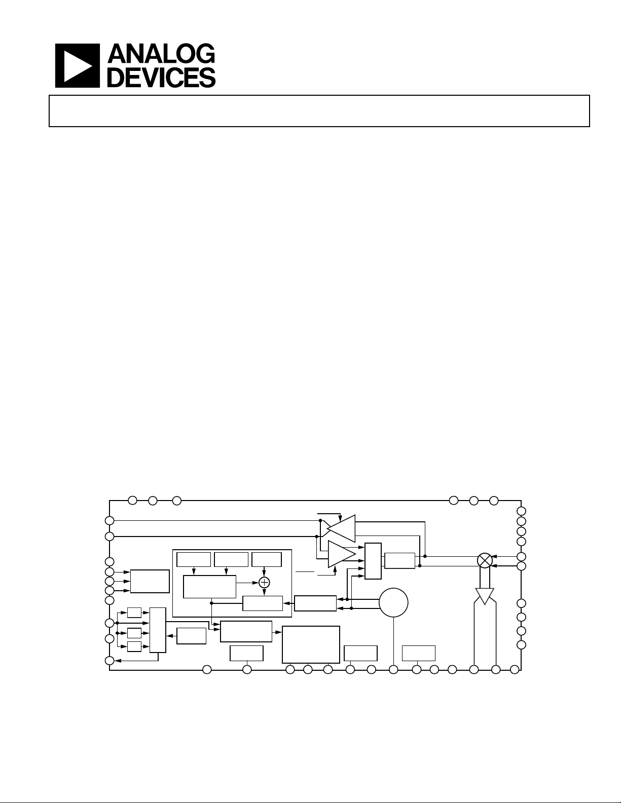
GENERAL DESCRIPTION
The ADRF6655 is a high dynamic range active mixer with
integrated PLL and VCO. The synthesizer uses a programmable
integer-N/fractional-N PLL to generate a local oscillator input
to the mixer. The PLL reference input is nominally 20 MHz. The
reference input can be divided by or multiplied by and then
applied to the PLL phase detector. The PLL can support input
reference frequencies from 10 MHz to 160 MHz. The phase
detector output controls a charge pump whose output is integrated
in an off-chip loop filter. The loop filter output is then applied to an
integrated VCO. The VCO output at 2 × f
oscillator (LO) divider as well as to a programmable PLL divider.
is then applied to a local
LO
ADRF6655
The programmable divider is controlled by an Σ-Δ modulator
(SDM). The modulus of the SDM can be programmed between
1 and 2047.
The broadband, active mixer employs a bias adjustment to allow
for enhanced IP3 performance at the expense of increased supply
current. The mixer provides an input IP3 exceeding 25 dBm
with 12 dB single sideband NF under typical conditions. The IIP3
can be boosted to ~29 dBm with roughly 20 mA of additional
supplied current. The mixer provides a typical voltage conversion
gain of 6 dB with a 200 Ω differential IF output impedance. The
IF output can be externally matched to support upconversion over
a limited frequency range.
The ADRF6655 is fabricated using an advanced silicon-germanium
BiCMOS process. It is packaged in a 40-lead, exposed-paddle,
Pb-free, 6 mm × 6 mm LFCSP. Performance is specified over a
−40°C to +85°C temperature range.
FUNCTIONAL BLOCK DIAGRAM
CCLO
GNDGND
36
LON
37
38
LOP
11
GND
12
DATA
13
CLK
LE
GND
REFIN
GND
MUXOUT
Rev. 0
Information furnished by Analog Devices is believed to be accurate and reliable. However, no
responsibility is assumed by Analog Devices for its use, nor for any infringements of patents or other
rights of third parties that may result from its use. Specifications subject to change without notice. No
license is granted by implication or otherwise under any patent or patent rights of Analog Devices.
Trademarks and registered trademarks are the property of their respective owners.
14
15
6
7
8
INTERFACE
×2
÷2
÷4
SPI
35
MUX
34
FRACTION
REG
THIRD-ORDER
FRACTIONAL
INTERPOLATOR
TEMP
SENSOR
VCC1
LOSEL
MODULUS
1
INTEGER
REG
LOSEL
N COUNTER
21 TO 123
–
PHASE
+
FREQUENCY
DETECTOR
3.3V LDO VCO LDO2.5V LDO
2
DECL1
PRESCALER
CHARGE PUMP
250µA,
500µA (DEFAUL T),
750µA,
1000µA
3
CP
BUFFER
BUFFER
4
GND
9 105
RSET NC
DECL2 VCC2
MUX
DIVIDER
÷2 OR ÷3
VCO
CORE
39
VTUNE
Figure 1.
One Technology Way, P.O. Box 9106, Norwood, MA 02062-9106, U.S.A.
Tel: 781.329.4700 www.analog.com
Fax: 781.461.3113 ©2010 Analog Devices, Inc. All rights reserved.
40
DECL3
33
VCCLO
GND
NCNC
31
32
ADRF6655
19
181716
OUTP
OUTN
20
GND
30
29
28
27
26
25
24
23
22
21
GND
IP3SET
GND
VCCMIX
INP
INN
GND
GND
VCCV2I
GND
8817-001
Page 2

ADRF6655
TABLE OF CONTENTS
Features .............................................................................................. 1
General Description ......................................................................... 1
Functional Block Diagram .............................................................. 1
Revision History ............................................................................... 2
Specifications ..................................................................................... 3
Timing Characteristics ................................................................ 5
Absolute Maximum Ratings ............................................................ 6
ESD Caution .................................................................................. 6
Pin Configuration and Function Despcriptions .......................... 7
Typical Performance Characteristics ............................................. 9
Downconversion ........................................................................... 9
Upconversion .............................................................................. 11
PLL Characteristic ...................................................................... 12
Complimentary Cumulative Distribution Function (CCDF):
Downconversion, LO = 1100 MHz, RF = 900 MHz .............. 14
Complimentary Cumulative Distribution Function (CCDF):
Downconversion, LO = 1700 MHz, RF = 1900 MHz ............ 15
Complimentary Cumulative Distribution Function (CCDF):
Upconversion Distribution ....................................................... 16
Circuit Description ......................................................................... 17
PLL and VCO Block ................................................................... 17
RF Mixer Block ........................................................................... 17
Digital Interfaces ........................................................................ 18
Analog Interfaces ............................................................................ 19
Supply Connections ................................................................... 19
Synthesizer Connections ........................................................... 19
Output Matching and Biasing................................................... 19
Input Matching ........................................................................... 20
IP3SET Linearization Feature ................................................... 21
CDAC Linearization Feature .................................................... 21
External LO Interface ................................................................ 21
Using an External VCO ............................................................. 22
ADRF6655 Control Software ........................................................ 23
PLL Loop Filter Design ............................................................. 23
Register Structure ........................................................................... 24
Device Programming ................................................................. 25
Initialization Sequence .............................................................. 25
Register 0—Integer Divide Control ......................................... 26
Register 1—Modulus Divide Control ...................................... 27
Register 2—Fractional Divide Control .................................... 27
Register 3—Σ-Δ Modulator Dither Control ........................... 28
Register 4—Charge Pump, PFD, and Reference
Path Control ................................................................................ 29
Register 5—LO Path and Mixer Control ................................. 31
Register 6—VCO Control and PLL Enables ........................... 32
Register 7—External VCO Control ......................................... 33
Characterization Setups ................................................................. 34
Evaluation Board Layout and Thermal Grounding ................... 38
Outline Dimensions ....................................................................... 41
Ordering Guide .......................................................................... 41
REVISION HISTORY
2/10—Revision 0: Initial Version
Rev. 0 | Page 2 of 44
Page 3

ADRF6655
SPECIFICATIONS
VCC = 5 V; ambient temperature (TA) = 25°C; REFIN = 20 MHz, phase frequency detector (PFD) frequency = 20 MHz, IF output loaded
into 4-to-1 transformer matched to a 50 Ω system, unless otherwise noted.
Table 1.
Parameter Test Conditions/Comments Min Typ Max Unit
RF INPUT FREQUENCY RANGE 100 2500 MHz
IF OUTPUT FREQUENCY RANGE
Can be matched externally for improved return loss at higher
frequencies (see the Output Matching and Biasing section)
INTERNAL LO FREQUENCY RANGE Divide-by-3 mode
Divide-by-2 mode
1
1
EXTERNAL LO FREQUENCY RANGE Divide-by-2 mode2 500 2300 MHz
MIXER
Input Return Loss
Output Return Loss
INP, INN; relative to 50 Ω, from 350 MHz to 2200 MHz using
TC1-1-13M+ balun
OUTP, OUTN; relative to 50 Ω out to 200 MHz using TC4-1W
output transformer option
3
3
IF Output Impedance OUTP, OUTN 200 Ω
Output Common Mode OUTP, OUTN; external pull-up balun or inductors required V
Voltage Conversion Gain IF output loaded into 200 Ω differential load 6 dB
Output Swing 2 V p-p
LO-to-IF Output Leakage Can be improved using external filtering −40 dBm
DYNAMIC PERFORMANCE IP3Set = 3.2 V
Upconversion
340 MHz RF input, 1200 MHz IF output using 1540 MHz
LO (see Figure 56 for output matching network)
Gain Flatness
Over ±50 MHz bandwidth for 1200 MHz output center
frequency
Gain Temperature Coefficient Average values from −40°C to +85°C −10
Output P1dB 11 dBm
Second-Order Output Intercept (IIP2) −5 dBm each tone 60 dBm
Third-Order Output Intercept (IIP3) −5 dBm each tone, IP3SET = 3.2 V 31 dBm
−5 dBm each tone, IP3SET = open 28 dBm
Output Noise Spectral Density IP3SET = 3.2 V, RF input terminated with 50 Ω −160 dBm/Hz
IP3SET = 3.2 V, RF input = −5 dBm, f
= 380 MHz applied, measured noise at fIF = 915 MHz
f
RF
= 1315 MHz with
LO
Downconversion 1880 MHz RF input, 140 MHz IF output using 1740 MHz LO
Gain Flatness
Over ±50 MHz bandwidth for 1880 MHz input center
frequency
Gain Temperature Coefficient Average values from −40°C to +85°C −10
Input P1dB IP3SET = 3.2 V 14 dBm
IP3SET = open 12 dBm
Second-Order Input Intercept (IIP2) −5 dBm each tone 50 dBm
Third-Order Input Intercept (IIP3) −5 dBm each tone, IP3SET = 3.2 V 27 dBm
−5 dBm each tone, IP3SET = open 26 dBm
SSB Noise Figure (NF) IP3SET = 3.2 V 14 dB
IP3SET = open 12 dB
SSB Noise Figure Under Blocking
Conditions
−5 dBm RF input blocker applied at 995 MHz, fLO = 1200 MHz,
noise measured at 5 MHz offset from IF output blocker
IP3SET = 3.2 V 20.75 dB
IP3SET = open 20.25 dB
IF/2 Spurious −5 dBm RF input power −65 dBc
LO OUTPUT LOP, LON
Output Level 1 × LO into a 50 Ω load, LO buffer enabled −7 dBm
LF 2200 MHz
1050 1530 MHz
1530 2300 MHz
12 dB
12 dB
V
POS
0.25 dB p-p
mdB/°C
−155 dBm/Hz
0.25 dB p-p
mdB/°C
Rev. 0 | Page 3 of 44
Page 4

ADRF6655
Parameter Test Conditions/Comments Min Typ Max Unit
SYNTHESIZER SPECIFICATIONS Synthesizer specifications referenced to 1 × LO4
Fundamental VCO Sensitivity VCO tuning sensitivity before divide-by-2 or divide-by-3 75 MHz/V
Spurs Measured at LO output
Reference/PFD Spurs f
f
2 × f
4 × f
Phase Noise PFD frequency = 20 MHz
LO Frequency = 1330 MHz
@ 10 kHz offset −85 dBc/Hz
@ 100 kHz offset −114 dBc/Hz
@ 1 MHz offset −138 dBc/Hz
@ 10 MHz offset −154 dBc/Hz
Integrated Phase Noise 10 kHz to 40 MHz integration bandwidth 0.3 °rms
LO Frequency = 1840 MHz
@ 10 kHz offset −83 dBc/Hz
@ 100 kHz offset −111 dBc/Hz
@ 1 MHz offset −136 dBc/Hz
@ 10 MHz offset −152 dBc/Hz
Integrated Phase Noise 10 kHz to 40 MHz integration bandwidth 0.4 °rms
PFD Frequency 19.33 20 40 MHz
REFERENCE CHARACTERISTICS REFIN, MUXOUT
REFIN Input Frequency 10 20 160 MHz
REFIN Input Capacitance 4 pF
REFIN Input Current ±100 μA
REFIN Input Sensitivity AC-coupled 0.25 1 3.3 V p-p
MUXOUT Output Levels VOL (lock detect output selected) 0.25 V
V
CHARGE PUMP CP
Pump Current
Output Compliance Range 1 2.8 V
LOGIC INPUTS CLK, DATA, LE
V
, Input High Voltage 1.4 3.3 V
INH
V
, Input Low Voltage 0 0.7 V
INL
I
, Input Current ±1 μA
INH/IINL
CIN, Input Capacitance 3 pF
POWER SUPPLIES VCC1, VCC2, VCCLO
Voltage Range 4.75 5 5.25 V
Supply Current LO output buffer disabled
PLL only 115 mA
Normal TX mode, IP3SET = 3.2 V, fLO ≤1530 MHz (divide-by-3) 310 mA
Normal TX mode, IP3SET = 3.2 V, fLO > 1530 MHz (divide-by-2) 270 mA
Normal RX mode, IP3SET = open, fLO ≤ 1530 MHz (divide-by-3) 285 mA
Normal RX mode, IP3SET = open, fLO > 1530 MHz (divide-by-2) 245 mA
Power-down mode 15 mA
1
Internal LO path divider programmed via serial interface. See the section for additional information. LO Signal Chain
2
See the section. External LO Interface
3
Improved return loss can be achieved using external matching. See the section for more details. Circuit Description
4
Measured on standard evaluation board with 1.5 kHz loop filter (C13 = 47 nF, C14 = 0.1 μF, C15 = 4.7 μF, R9 = 270 Ω, R10 = 68 Ω).
/2 −95 dBc
PFD
−83 dBc
PFD
−85 dBc
PFD
−88 dBc
PFD
(lock detect output selected) 2.7 V
OH
Charge pump current adjustable using Register 4 and/or
(see Pin 5 description)
R
SET
4
500 μA
Rev. 0 | Page 4 of 44
Page 5
ADRF6655
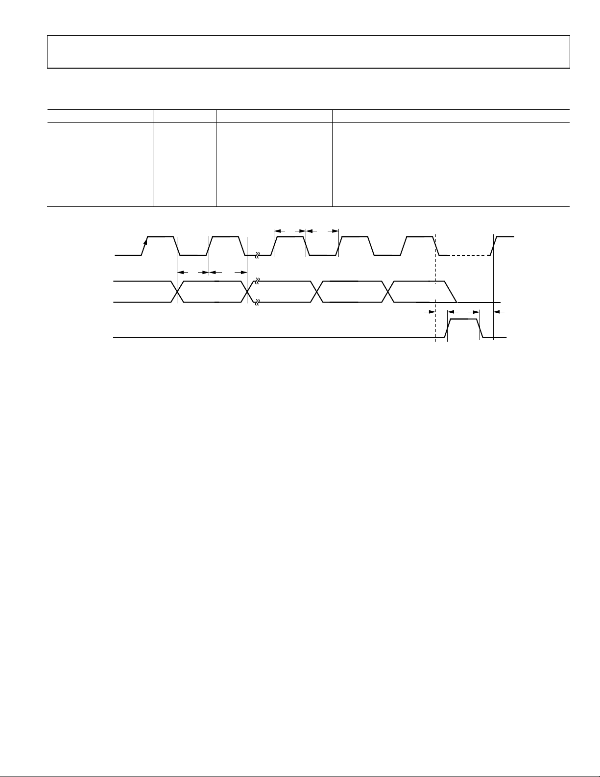
TIMING CHARACTERISTICS
Table 2. Serial Interface Timing, VCC = 5 V ± 5%
Parameter Limit Unit Test Conditions/Comments
t1 20 ns minimum LE setup time
t2 10 ns minimum DATA to CLK setup time
t3 10 ns minimum DATA to CLK hold time
t4 25 ns minimum CLK high duration
t5 25 ns minimum CLK low duration
t6 10 ns minimum CLK to LE setup time
t7 20 ns minimum LE pulse width
CLK
t
4
t
5
DATA
DB23 (MSB) DB22
LE
t
2
t
3
DB2 DB1
(CONTROL BIT C2)(CONTROL BIT C3)
DB0 (LSB)
(CONTROLBIT C1)
t
t
t
7
6
1
08817-002
Figure 2. Timing Diagram
Rev. 0 | Page 5 of 44
Page 6
ADRF6655
ABSOLUTE MAXIMUM RATINGS
Table 3.
Parameter Rating
Supply Voltage, VCC 5.5 V
Digital I/O CLK, DATA, LE −0.3 V to +3.6 V
OUTP, OUTN VCC
LOP, LON 16 dBm
INN, INP 20 dBm
DECL3 Using External Bias Option 3.5 V
θJA (Exposed Paddle Soldered Down)1 35°C/W
Maximum Junction Temperature 150°C
Operating Temperature Range −40°C to +85°C
Storage Temperature Range −65°C to +150°C
1
Per JDEC standard JESD 51-2. For information on optimizing thermal
impedance, see the Evaluation Board Layout and Thermal Grounding
section.
Stresses above those listed under Absolute Maximum Ratings
may cause permanent damage to the device. This is a stress
rating only; functional operation of the device at these or any
other conditions above those indicated in the operational
section of this specification is not implied. Exposure to absolute
maximum rating conditions for extended periods may affect
device reliability.
ESD CAUTION
Rev. 0 | Page 6 of 44
Page 7
ADRF6655
PIN CONFIGURATION AND FUNCTION DESPCRIPTIONS
ND
C
NC
33
G
N
32
31
VCO
LDO
VCCLO
GND
GND
LON
LOP
VTUNE
DECL3
34
35
36
37
38
39
40
1VCC1
2DECL1
3CP
4GND
5RSET
6REFIN
7GND
8MUXOUT
9DECL2
10VCC2
NC = NO CONNECT
3.3V
LDO
ENABLE
2.5V
LDO
PD +
CHARGE
PUMP
×2
÷2 OR ÷4
PFD
MUX
FRACTION
11
GND
12
DATA
THIRD-ORDER
MODULUS
SERIAL
PORT
13
CLK
VCO
BAND
AND
CURRENT
CAL/SET
PROGRAMMABLE
DIVIDER
SDM
INTEGER
15
14
LE
GND
ADRF6655
WIDEBAND
UP/DOWN
CONVERTER
6
VCO
6
CORE
16
NC
PRESCALER
17
18
UTN
O
VCCLO
MUX
÷2 OR ÷3
19
OUTP
20
GND
30 GND
29 IP3SET
28 GND
27 VCCMIX
26 INP
25 INN
24 GND
23 GND
22 VCCV2I
21 GND
08817-003
Figure 3. Pin Configuration
Table 4. Pin Function Descriptions
Pin No. Mnemonic Description
1 VCC1
Power Supply for Internal 3.3 V LDO. The power supply voltage range is 4.75 V to 5.25 V. Supply pin should
be decoupled with 100 pF and 0.1 μF capacitors located close to the pin.
2 DECL1
Decoupling Node for 3.3 V LDO. Pin should be decoupled with 100 pF, 0.1 μF, and 10 μF capacitors
located close to the pin.
3 CP Charge Pump Output Pin. Connect this pin to V
4, 7, 11, 15,
GND Ground. Connect these pins to a low impedance ground plane.
20, 21, 23,
24, 28, 30,
31, 35, 36
Rev. 0 | Page 7 of 44
through the loop filter.
TUNE
Page 8

ADRF6655
Pin No. Mnemonic Description
5 RSET
6 REFIN
8 MUXOUT
9 DECL2
10 VCC2
12 DATA Serial Data Input. The serial data input is loaded MSB first with the three LSBs being the control bits.
13 CLK
14 LE
16, 32, 33 NC No Connection.
17, 34 VCCLO
18,19 OUTN, OUTP Mixer IF Outputs. These pins should be pulled to VCC with RF chokes.
22 VCCV2I
25, 26 INN, INP Mixer RF Inputs. Differential RF Inputs. Internally matched to 50 Ω. This pin must be ac-coupled.
27 VCCMIX
29 IP3SET Connect Resistor to VCC to Adjust IP3.
37, 38 LON, LOP
39 VTUNE
40 DECL3
EPAD (EP) The exposed paddle should be soldered to a low impedance ground plane.
Charge Pump Current. The nominal charge pump current can be set to either 250 μA, 500 μA, 750 μA,
or 1 mA using DB10 and DB11 of Register 4 and by setting DB18 to 0 (internal reference current).
In this mode, no external R
) can be externally tweaked according to
(I
NOMINAL
⎡
[]
RSET
where I
CP, BASE
=Ω
⎢
⎣
is the base charge pump current in μA.
is required. If DB18 is set to 1, the four nominal charge pump currents
SET
4.217
I
×
250
⎤
,
BASECP
⎥
⎦
8.37
−
For further details on the charge pump current,see the Register 4—Charge Pump, PFD, and Reference
Path Control section.
Reference Input. Nominal input level is 1 V p-p. Input range is 10 MHz to 160 MHz. This pin must be
ac-coupled.
Multiplexer Output. This output allows either a digital lock detect, a voltage proportional to temperature,
or a buffered, frequency-scaled reference signal to be accessed externally. The output is selected by
programming the appropriate bits in Register 4.
Decoupling Node for 2.5 V LDO. Pin should be decoupled with 100 pF, 0.1 μF, and 10 μF capacitors
located close to the pin.
Power Supply for Internal 2.5 V LDO. The power supply voltage range is 4.75 V to 5.25 V. Supply pin
should be decoupled with 100 pF and 0.1 μF capacitors located close to the pin.
Serial Clock Input. This serial clock input is used to clock in the serial data to the registers. The data
is latched into the 24-bit shift register on the CLK rising edge. Maximum clock frequency is 20 MHz.
Load Enable. When the LE input pin goes high, the data stored in the shift registers is loaded into one
of the six registers, the relevant latch being selected by the first three control bits of the 24-bit word.
Power Supply for LO Path. The power supply voltage range is 4.75 V to 5.25 V. Supply pin should be
decoupled with 100 pF and 0.1 μF capacitors located close to the pin.
Power Supply for Voltage to Current Input Stage. The power supply voltage range is 4.75 V to 5.25 V.
Supply pin should be decoupled with 100 pF and 0.1 μF capacitors located close to the pin.
Power Supply for Mixer. The power supply voltage range is 4.75 V to 5.25 V. Supply pin should be
decoupled with 100 pF and 0.1 μF capacitors located close to the pin.
Local Oscillator Input/Output. The internally generated 1 × f
LO generation is disabled, an external 2 × f
or 3 × fLO (depending on divider selection) can be applied
LO
is available on these pins. When internal
LO
to these pins. This pin must be ac-coupled.
VCO Control Voltage Input. This pin is driven by the output of the loop filter. Nominal input voltage
range on this pin is 1 V to 2.8 V.
Decoupling Node for VCO LDO. Connect a 100 pF capacitor and a 10 μF capacitor between this pin
and ground.
Rev. 0 | Page 8 of 44
Page 9
ADRF6655
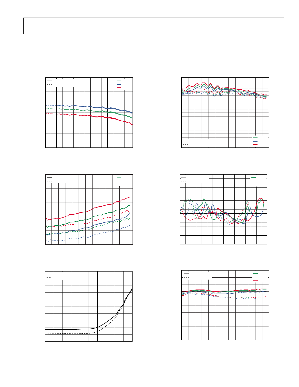
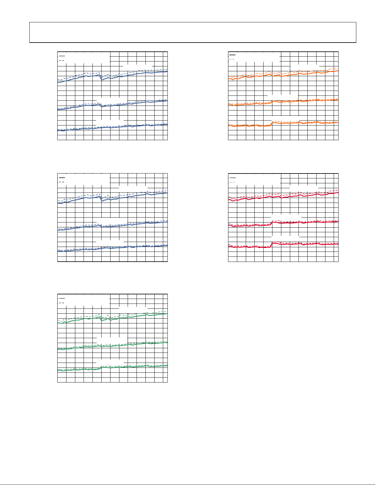
TYPICAL PERFORMANCE CHARACTERISTICS
VS = 5 V, TA = 25°C, PFD = 20 MHz, REFIN = 20 MHz, IP3SET = 3.2 V, unless otherwise noted.
DOWNCONVERSION
Measured using typical downconversion circuit schematic with high-side LO and 140 MHz IF output, unless otherwise noted.
5
LOW-SIDE LO
HIGH-SIDE L O
4
3
2
1
0
GAIN (dB)
–1
–2
–3
–4
–5
900 1100130015001700190021002300
INPUT FREQUENCY (MHz)
Figure 4. Conversion Gain vs. Input Frequency
20
IP3SET = 3.2V
IP3SET = OPEN
18
16
14
NOISE FI G URE (d B)
12
10
900 1100 1300 1500 1700 1900 2100
RF FREQUENC Y ( MHz)
Figure 5. SSB Noise Figure vs. RF Frequency
30
IP3SET = 3.2V
IP3SET = OPEN
28
26
24
22
20
18
NOISE FI GURE (dB)
16
14
12
10
–50 –45 –40 –35 –30 –25 –20 –15 –10 –5 0
CW BLOCKER LEVEL (dBm)
Figure 6. SSB Noise Figure vs. CW Blocker Level
+25°C
–40°C
+85°C
+25°C
–40°C
+85°C
08817-086
08817-123
08817-104
32
31
30
29
28
27
26
25
24
23
22
21
20
19
INPUT IP3 (dBm)
18
17
16
15
14
IP3SET = 3 .2V
13
IP3SET = OPEN
12
900 1100 1300 1500 1700 1900 2100
INPUT FREQ UE NC Y ( MHz )
Figure 7. Input IP3 vs. Input Frequency
100
LOW-SIDE LO
95
HIGH-SIDE LO
90
85
80
75
70
65
60
55
50
INPUT IP2 (dBm)
45
40
35
30
25
20
900 1100 1300 1500 1700 1900 2100 2300 2500
INPUT FREQUENCY (MHz)
Figure 8. Input IP2 vs. Input Frequency
20
IP3SET = 3 .2V
19
IP3SET = OPEN
18
17
16
15
14
13
12
11
10
9
8
7
INPUT P1 dB (dBm)
6
5
4
3
2
1
0
900 1100 1300 1500 1700 1900 2100
INPUT FREQUENCY (MHz)
Figure 9. Input P1dB vs. Input Frequency
+25°C
–40°C
+85°C
+25°C
–40°C
+85°C
+25°C
–40°C
+85°C
08817-087
8817-088
08817-089
Rev. 0 | Page 9 of 44
Page 10
ADRF6655
–
–
0
–5
–10
–15
–20
–25
S11 (dB)
–30
–35
–40
–45
0 500 1000 1500 2000 2500 3000
FREQUENCY ( M Hz )
Figure 10. RF Port Input Return Loss (S11) vs.
Frequency Measured through TC1-1-13M+
300
270
240
210
180
150
120
90
OUTPUT RESISTANCE (Ω)
60
30
0
50 100 150 200 250 300 350 400 4500500
FREQUENCY ( MHz)
Figure 11. IF Port Output Impedance vs. Frequency
40
–45
–50
–55
–60
–65
–70
–75
–80
–85
LO-TO-RF I NP UT LEAKAGE (dBm)
–90
–95
–100
1050 1250 1450 1650 1850 2050 2250
LO FREQUENCY (MHz)
Figure 12. LO-to-RF Input Port Leakage vs. LO Frequency
+25°C
–40°C
+85°C
2.0
1.8
1.6
1.4
1.2
1.0
0.8
0.6
0.4
0.2
0
08817-122
OUTPUT CAPACITANCE (pF)
08817-124
08817-090
400
380
360
340
320
300
280
260
240
220
200
180
160
140
120
SUPPLY CURRENT ( mA)
100
80
60
40
IP3SET = 3.2 V
20
IP3SET = OPEN
0
1050 1250 1450 1650 1850 2050 2250
LO FREQ UENCY ( M Hz )
Figure 13. Supply Current vs. LO Frequency
0
–1
–2
–3
–4
–5
–6
–7
–8
–9
–10
–11
–12
–13
–14
–15
LO OUTP UT POWER (dBm)
–16
–17
–18
–19
–20
1050 1250 1450 1650 1850 2050 2250
LO FREQ UE NCY (M Hz )
Figure 14. LO Port Output Power vs. LO Frequency
20
–25
–30
–35
–40
–45
–50
–55
–60
–65
–70
LO-TO-IF OUTPUT LE AKAG E (dBm)
–75
–80
1050 1150 1250 1350 1450 1550 1650 1750 1850 1950 2050 2150 2250
LO FREQUE NCY (MHz)
Figure 15. LO-to-IF Output Port Leakage vs. LO Frequency
+25°C
–40°C
+85°C
+25°C
–40°C
+85°C
+25°C
–40°C
+85°C
08817-091
08817-092
08817-014
Rev. 0 | Page 10 of 44
Page 11
ADRF6655
–
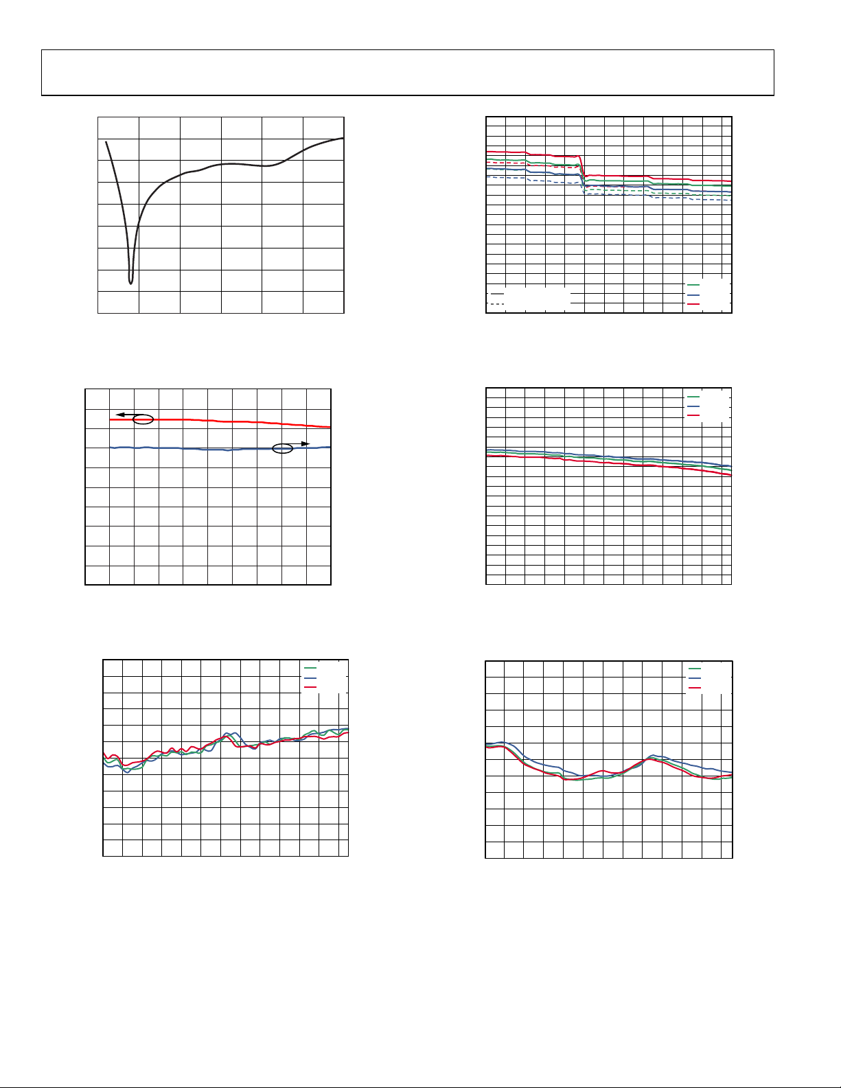
UPCONVERSION
Measured using typical upconversion circuit schematic with high-side LO and 340 MHz RF input, unless otherwise noted.
5
4
3
2
1
0
GAIN (dB)
–1
–2
–3
–4
–5
710 810 910 1010 1110 1210 1310 1410 1510 1610
OUTPUT FREQUE NC Y ( M H z )
Figure 16. Conversion Gain vs. Output Frequency
0
–10
–20
–30
–40
–50
–60
SPURIOUS RESPONSE (dBc)
–70
RF
f
–80
– 2 ×
LO
–90
f
–100
1050 1150 1250 1350 1450 1550 1650 1750 1850 1950 2050 2150 2250
LO FREQ UENCY ( M Hz )
+25°C
–40°C
+85°C
+25°C
–40°C
+85°C
8817-093
08817-016
35
IP3SET = 3 .2V
34
IP3SET = OPEN
33
32
31
30
29
28
27
26
25
OUTPUT IP3 (dBm)
24
23
22
21
20
710 810 910 1010 1110 1210 1310 1410 1510 1610
OUTPUT FREQUENCY (M H z)
Figure 19. Output IP3 vs. Output Frequency
20
19
IP3SET = 3.2V
18
IP3SET = OPEN
17
16
15
14
13
12
11
10
9
8
7
OUTPUT P1dB (dBm)
6
5
4
3
2
1
0
710 810 910 1010 1110 1210 1310 1410 1510 1610
OUTPUT F RE QUENCY (MHz)
+25°C
–40°C
+85°C
+25°C
–40°C
+85°C
8817-094
08817-095
Figure 17. f
− 2 × fRF Spurious Response vs.
LO
LO Frequency (Relative to IF Output Power)
0
–10
–20
–30
–40
–50
–60
LO-TO-IF OUTPUT LEAKAGE (dBm)
–70
–80
1050 1150 1250 1350 1450 1550 1650 1750 1850 1950 2050
LO FREQ UENCY (MHz)
Figure 18. LO-to-IF Output Leakage vs. Frequency
+25°C
–40°C
+85°C
08817-105
Rev. 0 | Page 11 of 44
Figure 20. Output P1dB vs. Output Frequency
100
–110
–120
–130
–140
–150
–160
NOISE SPECTRAL DENSITY ( dBm/Hz)
–170
710 810 910 1010 1110 1210 1310 1410 1510 1610
OUTPUT F RE QUENCY (MHz)
Figure 21. Output Noise Spectral Density vs. Output Frequency
8817-121
Page 12
ADRF6655
A
A
A
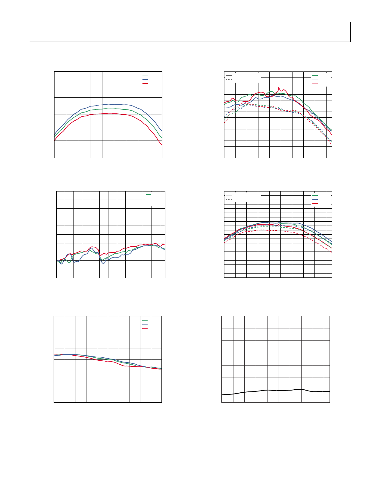
PLL CHARACTERISTIC
Measured using typical downconversion circuit schematic with high-side LO and 140 MHz IF output, loop filter = 1.5 kHz, unless
otherwise noted.
0
–10
–20
–30
–40
–50
–60
–70
–80
–90
–100
–110
–120
PHASE NOISE ( dBc/Hz)
–130
–140
–150
–160
–170
1k 10k 100k 1M 10M 100M
LO = 2275MHz
LO = 1100MHz
OFFSET FREQUENCY ( kHz)
+25°C
–10°C
–40°C
+70°C
+85°C
08817-021
Figure 22. Typical Fractional-N Phase Noise Plot
1.0
0.9
0.8
0.7
0.6
0.5
0.4
TED PHASE NOI S E (° C rms)
0.3
0.2
INTEGR
0.1
0
1050 1150 1250 1350 1450 1550 1650 1750 1850 1950 2050 2150 2250
LO FREQ UENCY (MHz)
+25°C
–10°C
–40°C
+70°C
+85°C
08817-022
Figure 23.10 kHz to 40 MHz Integrated Phase Noise vs. LO Frequency
2500
2000
1500
1000
500
2.290G
TION FROM 2.29GHz (Hz)
–500
–1000
–1500
–2000
FREQUENCY DEVI
–2500
025
1
10
TIME (ms)
1: 10ms 2.289999883GHz
08817-120
Figure 24. Lock Time for 10 MHz Step with 1.5 kHz Loop Filter
0
1 × PFD OFFSET
2 × PFD OFFSET
–10
4 × PFD OFFSET
–20
–30
–40
–50
–60
–70
–80
–90
LO REFERENCE P F D SP URS (d Bc)
–100
–110
1050 1250 1450 1650 1850 2050 2250
LO FREQ UE NCY (M Hz )
Figure 25. LO Reference/PFD Spurs vs. LO Frequency
3.0
2.9
2.8
2.7
2.6
2.5
2.4
2.3
2.2
2.1
2.0
1.9
VTUNE (V)
1.8
1.7
1.6
1.5
1.4
1.3
1.2
1.1
1.0
HIGH-SIDE LO
LOW-SIDE LO
1050 1150 1250 1350 1450 1550 1650 1750 1850 1950 2050 2150 2250
LO FREQ UENCY (MHz)
Figure 26. Tuning Voltage vs. LO Frequency
1.9
LO = 1100MHz, IP3SET = 3.2V
1.8
1.7
T (V)
1.6
VPT
1.5
1.4
1.3
–40 –30 –20 –10 0 10 20 30 40 50 60 70 80
LO = 2300MHz, IP3SET = 3.2V
LO =2300MHz, IP3SET = OPEN
TEMPERATURE (°C)
Figure 27. VPTAT MUXOUT Voltage vs. Temperature
+25°C
–40°C
+85°C
+25°C
–40°C
+85°C
08817-096
08817-025
8817-097
Rev. 0 | Page 12 of 44
Page 13
ADRF6655
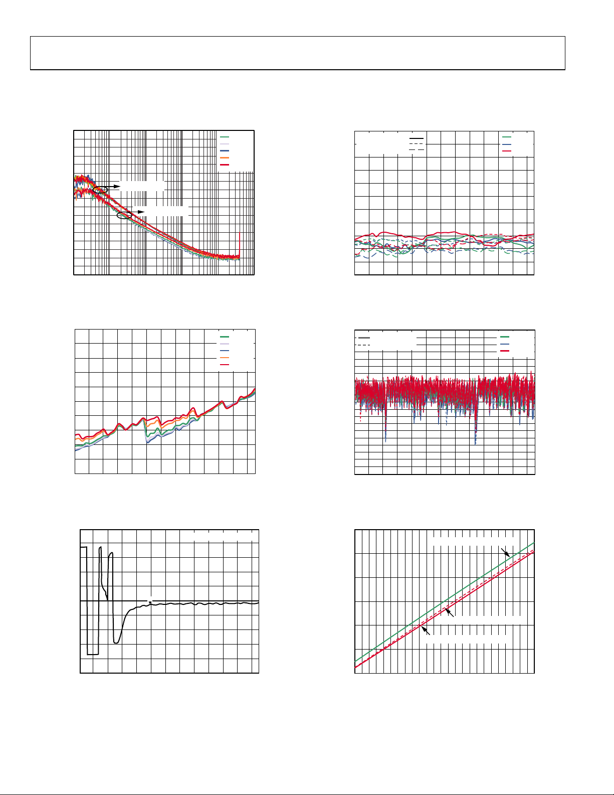
–
–
–
–
–
60
AVERAGE
–65
AVERAGE + 3 × ST DEV
–70
–75
–80
–85
–90
–95
–100
–105
–110
–115
–120
PHASE NOISE ( dBc/Hz)
–125
–130
–135
–140
–145
–150
1050 1150 1250 1350 14501550 1650 1750 1850 1950 2050 2150 2250
100kHz OFFS E T
1MHz OFFSET
LO FREQUENCY (MHz)
10kHz OFFSET
08817-039
Figure 28. −40°C Spot Phase Noise vs. LO Frequency
60
AVERAGE
–65
AVERAGE + 3 × ST DEV
–70
–75
–80
–85
–90
–95
–100
–105
–110
–115
–120
PHASE NOISE (dBc/Hz)
–125
–130
–135
–140
–145
–150
1050 1150 1250 1350 14501550 1650 1750 1850 1950 2050 2150 2250
100kHz OFFS E T
1MHz OFFSET
LO FREQUENCY (MHz)
10kHz OFFS ET
08817-040
Figure 29. −10°C Spot Phase Noise vs. LO Frequency
60
AVERAGE
–65
AVERAGE + 3 × ST DEV
–70
–75
–80
–85
–90
–95
–100
–105
–110
–115
–120
PHASE NOISE (dBc/Hz)
–125
–130
–135
–140
–145
–150
1050 1150 1250 1350 14501550 1650 1750 1850 1950 2050 2150 2250
100kHz OFFS E T
1MHz OFFSET
LO FREQUENCY (MHz)
10kHz OFFS ET
08817-041
Figure 30. 25°C Spot Phase Noise vs. LO Frequency
60
AVERAGE
–65
AVERAGE + 3 × S T DEV
–70
–75
–80
–85
–90
–95
–100
–105
–110
–115
–120
PHASE NOISE (dBc/Hz)
–125
–130
–135
–140
–145
–150
1050 1150 1250 1350 14501550 1650 1750 1850 1950 2050 2150 2250
100kHz OFF S E T
1MHz OFF S E T
LO FREQUENCY (MHz)
10kHz OFF S E T
08817-042
Figure 31. 70°C Spot Phase Noise vs. LO Frequency
60
AVERAGE
–65
AVERAGE + 3 × S T DEV
–70
–75
–80
–85
–90
–95
–100
–105
–110
–115
–120
PHASE NOISE (dBc/Hz)
–125
–130
–135
–140
–145
–150
1050 1150 1250 1350 1450 1550 1650 1750 1850 1950 2050 2150 2250
100kHz OFFSET
1MHz OFF S E T
LO FREQUENCY (MHz)
10kHz OFFS ET
08817-043
Figure 32. 85°C Spot Phase Noise vs. LO Frequency
Rev. 0 | Page 13 of 44
Page 14
ADRF6655
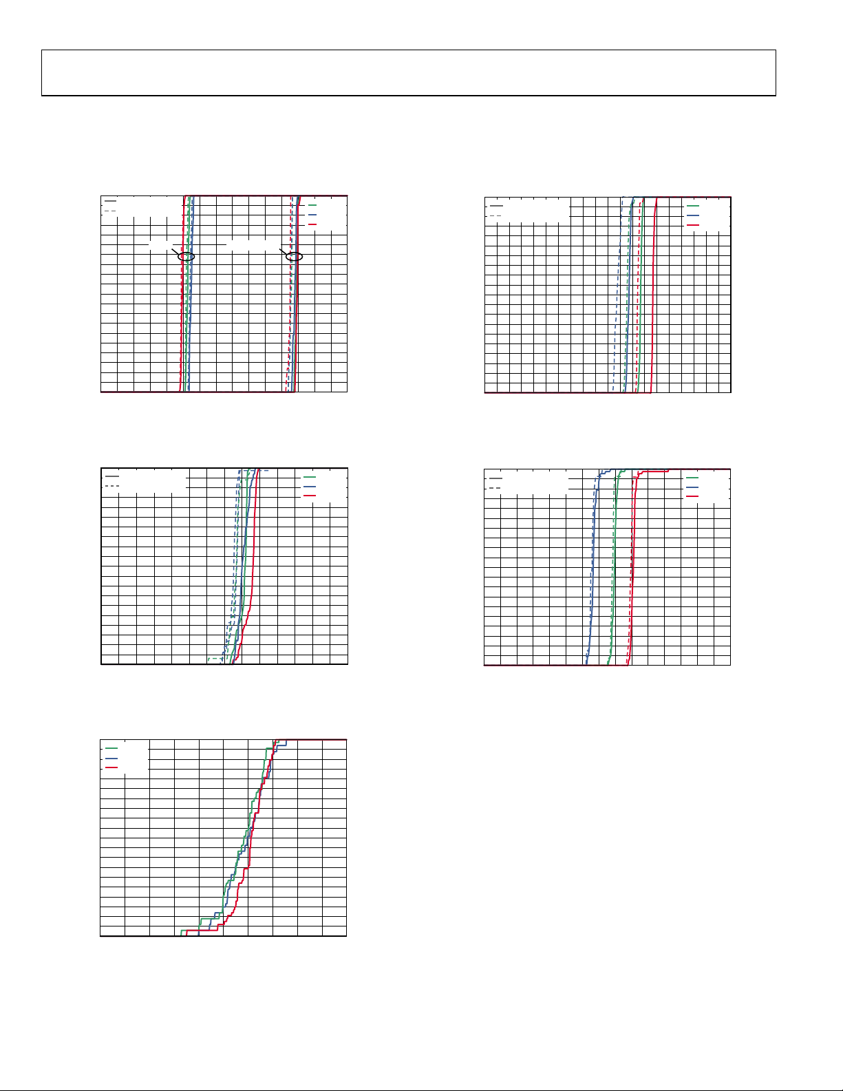
COMPLIMENTARY CUMULATIVE DISTRIBUTION FUNCTION (CCDF): DOWNCONVERSION, LO = 1100 MHz, RF = 900 MHz
VS = 5 V, TA = 25°C, PFD = 20 MHz, REFIN = 20 MHz, IP3SET = open, as measured using typical downconversion circuit schematic with
high-side LO and 200 MHz IF output, unless otherwise noted.
100
IP3SET = 3.2V
95
IP3SET = OPEN
90
85
80
75
70
65
60
55
50
45
40
35
30
25
20
DISTRIBUT ION PERCENTAGE (%)
15
10
5
0
–10 –8 –6 –4 –2 0 2 4 6 8 10 12 14 16 18 20
GAIN
GAIN (dB), INPUT P1dB (dBm)
INPUT P1dB
+25°C
–40°C
+85°C
08817-106
Figure 33. Gain and Input P1dB CCDF
100
IP3SET = 3.2V
95
IP3SET = OPEN
90
85
80
75
70
65
60
55
50
45
40
35
30
25
20
DISTRIBUT ION PERCENTAGE (%)
15
10
5
0
12 14 16 18 20 22 24 26 28 30 32 34 36 38 40
INPUT IP3 (dBm)
+25°C
–40°C
+85°C
8817-107
Figure 34. Rx Input IP3 CCDF
100
+25°C
95
–40°C
90
+85°C
85
80
75
70
65
60
55
50
45
40
35
30
25
20
DISTRIBUTION PERCENTAGE (%)
15
10
5
0
–100 –95 –90 –85 –80 –75 –70 –65 –60 –55 –50
LO-TO-RF L E AKAGE (dBm)
08817-098
Figure 35. Rx LO-to-RF Leakage CCDF
Rev. 0 | Page 14 of 44
100
IP3SET = 3.2V
95
IP3SET = OPEN
90
85
80
75
70
65
60
55
50
45
40
35
30
25
20
DISTRIBUTION PERCENTAGE (%)
15
10
5
0
0 2 4 6 8 101214161820
NOISE FIGURE (dB)
+25°C
–40°C
+85°C
08817-108
Figure 36. Noise Figure CCDF
100
IP3SET = 3 .2V
95
IP3SET = OPEN
90
85
80
75
70
65
60
55
50
45
40
35
30
25
20
DISTRIBUT ION PERCENTAGE (%)
15
10
5
0
0 0.2 0.4 0.6 0.8 1.0 1.2 1.4 1.6 1.8 2.0 2.2 2.4 2.6 2.8 3.0
VPTAT (V)
+25°C
–40°C
+85°C
8817-109
Figure 37. VPTAT MUXOUT Voltage
Page 15

ADRF6655
COMPLIMENTARY CUMULATIVE DISTRIBUTION FUNCTION (CCDF): DOWNCONVERSION, LO = 1700 MHz, RF = 1900 MHz
VS = 5 V, TA = 25°C, PFD = 20 MHz, REFIN = 20 MHz, IP3SET = open, as measured using typical downconversion circuit schematic with
high-side LO and 200 MHz IF output, unless otherwise noted.
100
95
90
85
80
75
70
65
60
55
50
45
40
35
30
25
20
DISTRIBUTION PERCENTAGE (%)
15
10
5
0
–5 –4 –3 –2 –1 0 1
IP3SET = 3.2V
IP3SET = OPEN
GAIN
2 3 4 5 6 7 8 9 10 11 12 13 14 15 16 17 18 19 20
GAIN, INPUT P1dB (dB, dBm)
Figure 38. Gain and Input P1dB
100
IP3SET = 3.2V
95
IP3SET = OPEN
90
85
80
75
70
65
60
55
50
45
40
35
30
25
20
DISTRIBUTION PERCENTAGE (%)
15
10
5
0
20 21 22 23 24 25 26 27 28 29 30 31 32 33 34 35 36 37 38 39 40
INPUT IP3 (dBm)
Figure 39. Rx Input IP3
100
IP3SET = 3.2V
95
IP3SET = OPEN
90
85
80
75
70
65
60
55
50
45
40
35
30
25
20
DISTRIBUTION PERCENTAGE (%)
15
10
5
0
–100 –90 –80 –70 –60 –50 –40 –30
LO-TO-RF L E AKAGE (dBm)
Figure 40. Rx LO-to-RF Leakage
+25°C
–40°C
+85°C
INPUT P1dB
+25°C
–40°C
+85°C
+25°C
–40°C
+85°C
8817-033
08817-034
08817-099
Rev. 0 | Page 15 of 44
100
IP3SET = 3.2V
95
IP3SET = OPEN
90
85
80
75
70
65
60
55
50
45
40
35
30
25
20
DISTRIBUTION PERCENTAGE (%)
15
10
5
0
01234567891011121314151617181920
NOISE FI G URE (dB)
+25°C
–40°C
+85°C
08817-110
Figure 41. Rx Noise Figure CCDF
100
IP3SET = 3.2V
95
IP3SET = OPEN
90
85
80
75
70
65
60
55
50
45
40
35
30
25
20
DISTRIBUTION PERCENTAGE (%)
15
10
5
0
0.5 0.7 0.9 1.1 1.3 1.5 1.7 1.9 2.1 2.3 2.5
VPTAT (V)
+25°C
–40°C
+85°C
08817-038
Figure 42. VPTAT MUXOUT Voltage
Page 16

ADRF6655
COMPLIMENTARY CUMULATIVE DISTRIBUTION FUNCTION (CCDF): UPCONVERSION DISTRIBUTION
100
95
90
85
80
75
70
65
60
55
50
45
40
35
30
25
20
DISTRIBUT ION PERCENTAGE (%)
15
10
5
0
–10 –8 –6 –4 –2 0 2 4 6 8 10 12 14 16 18 20
GAIN
GAIN (dB), OUTPUT P1dB (dBm)
IP3SET = 3.2V
IP3SET = OPEN
OUTPUT P1dB
+25°C
–40°C
+85°C
Figure 43. Gain and Output P1dB CCDF, LO = 1220 MHz, RF = 340 MHz
100
IP3SET = 3.2 V
IP3SET = OPEN
90
80
70
60
50
40
30
20
DISTIBUTION PERCENTAGE (%)
10
0
0 5 10 15 20 25 30 35 40 45 50 55 60
OUTPUT I P 3 (dBm)
+25°C
–40°C
+85°C
Figure 44. Output IP3 CCDF, LO = 1220 MHz, RF = 340 MHz
100
IP3SET = 3.2V
95
IP3SET = OPEN
90
85
80
75
70
65
60
55
50
45
40
35
30
25
20
DISTRIBUTION PERCENTAGE (%)
15
10
5
0
–100 –90 –80 –70 –60 –50 –40 –30 –20 –10
LO-TO-IF OUTPUT LEAKAG E ( d Bm)
+25°C
–40°C
+85°C
Figure 45. LO-to-IF Output Leakage CCDF, LO = 1220 MHz, RF = 340 MHz
08817-100
8817-101
08817-113
100
90
80
70
60
50
40
30
20
DISTRIBUT ION PERCENTAGE (%)
10
0
–10–8–6–4–2 0 20
GAIN
OUTPUT P1dB
2 4 6 8 10 12 14 16 18
GAIN (dB), OUTPUT P1dB (dBm)
+25°C
–40°C
+85°C
IP3SET = 3. 2V
IP3SET = OP EN
08817-102
Figure 46. Gain and Output P1dB CCDF, LO = 1840 MHz, RF = 340 MHz
100
IP3SET = 3.2V
IP3SET = OPEN
90
80
70
60
50
40
30
20
DISTRIBUTION PERCENTAGE (%)
10
0
0 1020304050605 1525354555
OUTPUT IP3 (dBm)
+25°C
–40°C
+85°C
8817-103
Figure 47. Output IP3 CCDF, LO = 1840 MHz, RF = 340 MHz
100
95
IP3SET = 3.2V
90
IP3SET = OPEN
85
80
75
70
65
60
55
50
45
40
35
30
25
20
DISTRIBUTION PERCENTAGE (%)
15
10
5
0
–100 –90 –80 –70 –60 –50 –40 –30 –20 –10 0
LO-TO-IF PORT LEAKAGE (d Bm)
+25°C
–40°C
+85°C
08817-114
Figure 48. LO-to-IF Output Leakage CCDF, LO = 1840 MHz, RF = 340 MHz
Rev. 0 | Page 16 of 44
Page 17

ADRF6655
CIRCUIT DESCRIPTION
The ADRF6655 can be subdivided into a PLL and VCO block
and a mixer block. A detailed circuit description for each block
follows.
PLL AND VCO BLOCK
The PLL and VCO block, shown in Figure 49, is made up of a
reference input block, a phase and frequency detector (PFD), a
charge pump, a VCO, and a divide-by-N modulus block. An
off-chip loop filter completes the loop.
The VCO operates at twice the LO frequency for improved
isolation. The nominal value of Kv is 75 MHz/V at the VCO
output. As the VCO band is changed from 0 to 63, the size of the
varactor is also changed, thus maintaining a roughly constant
Kv across the entire operating range.
RF MIXER BLOCK
LO
VCC
LOOP
FILTER
×2
REFIN
÷2
÷4
ADRF6655 PLL BL OCK DIAGRAM
CP
CP
PFD
FRAC MOD INT
THIRD-ORDER
INTERPOLATOR
PROGRAMMABLE
DIVIDER
VTUNE
BAND
SELECT
PRESCALER
TO MIXER
BLOCk
Figure 49. PLL and VCO Block
The VCO is implemented with a single core that consists of 64
overlapping bands, as shown in Figure 50. The correct band is
selected automatically by the VCO band calibration circuit when
Register R0, Register R1, or Register R2 is programmed. The
VCO band selection takes roughly 4000 PFD cycles. During
calibration, an internal mux is used to disconnect the VCO input
voltage from the VTUNE pin and apply an internal reference
voltage for calibration. When calibration is complete, the VCO
input voltage is reconnected to the VTUNE pin and normal
PLL operation resumes.
2.4
2.2
2.0
/2 (GHz)
VCO
1.8
f
1.6
1.4
0.51.01.52.02.5
(V)
V
Figure 50. f
TUNE
/2 vs. Tuning Voltage for All 64 Bands
VCO
08817-052
VCO
÷2 OR ÷3
SIF
ADRF6655 MIXER BLOCK
CDAC
133Ω133Ω
V2I
OUTN
OUTP
IP3SET
RFIN
08817-053
Figure 51. Mixer Block
The mixer portion of the ADRF6655, shown in Figure 51, consists
of an LO signal chain, an RF voltage-to-current (V-to-I) converter,
and a mixer core. The LO chain receives a signal from either the
internal VCO or an external LO source. This LO signal then passes
through a frequency divider, which can be set to divide-by-2
8817-051
or divide-by-3, depending on the desired LO frequency. The
differential RF inputs are converted into currents by the V-to-I
converter and fed into the mixer core. A pair of 133 Ω pull-up
resistors are used to present a ~250 Ω source impedance at the
IF output.
LO Signal Chain
The LO chain consists of a mux that selects between the internal
VCO and an external LO source. The LO signal can then be
divided by 2 or divided by 3, providing a wide range of LO
frequencies from 1050 MHz to 2300 MHz. A buffer then drives
this divided down signal to the mixer core. The LO signal can
also be observed via the LO I/O port when the internal VCO
is selected. When the external LO buffer is enabled, the supply
current and die temperature increase, resulting in a slight
degradation of RF performance. In normal operation mode,
the external LO buffer should be disabled to help minimize
power consumption and provide optimal RF performance.
Rev. 0 | Page 17 of 44
Page 18

ADRF6655
V-to-I Converter
The differential RF input signal is applied to a pair of resistively
degenerated common-emitter stages, which converts the
differential input voltage to output currents. The input stage also
provides 50 Ω termination to the RF input port. The linearity
of this V-to-I stage can be optimized for a given frequency with
Pin IP3SET at the expense of power dissipation and noise figure.
An additional way of improving linearity without affecting
power dissipation or noise figure is provided by the CDAC
signal controlled by serial port interface (SPI).
Mixer Core
The mixer core, based on the Gilbert cell design of four crossconnected transistors, takes the currents from the V-to-I stage
and mixes them with the LO signal. This mixer core can be used
as a downconvert mixer as is or as an upconvert mixer with an
off-chip matching network for a given frequency range.
CHARGE PUMP
LOOP FILTER
DIGITAL INTERFACES
The ADRF6655 provides access to the many programmable
features available within the IC using a 3-wire SPI control
interface. The minimum delays and hold times are presented
in the timing diagram in Figure 2. The SPI interface provides
digital control of the internal PLL/VCO as well as several other
features related to the mixer core, on-chip referencing, and available
system monitoring functions. The MUXOUT pin provides access
to several output signals that can be selected via the SPI interface.
The available outputs are buffered, frequency-scaled versions of
the reference, a PLL lock-detect signal, and an internal voltage
that is proportional to the IC junction temperature. Details
regarding the register settings and initialization sequence are
included in the Register Structure section.
+5V
+5V
EXTERNAL
REFERENCE
MONITOR
OUTPUT
+5V
NC = NO CONNECT
RSET
VCC1
1
DECL1
2
CP
3
GND
4
RSET
5
REFIN
6
GND
7
8
MUXOUT
9
DECL2
10
VCC2
CONTROL
SPI
40
39
38
37
36
35
34
LOP
DECL3
VTUNE
LON
GND
GND
VCCLO
ADRF6655
GND
DATA
CLK
11
12
13
GND
LE
15
14
VCCLO
NC
16
17
+5V
33
NC
N
OUT
18
32
31
NC
GND
IP3SET
VCCMIX
VCCV2I
ND
OUTP
G
19
20
IF OUTPUT
MATCHING
BALUN AND BIAS
GND
GND
INP
INN
GND
GND
GND
30
29
28
27
26
25
24
23
22
21
V
SET
IF OUTPUT
+5V
RF INPUT
MATCHING
BALUN
+5V
RF INPUT
08817-054
Figure 52. Basic Circuit Connections
Rev. 0 | Page 18 of 44
Page 19

ADRF6655
A
A
ANALOG INTERFACES
The basic circuit connections for a typical ADRF6655 application
are presented in Figure 52.
SUPPLY CONNECTIONS
The ADRF6655 has several supply connections and on-board
regulated reference voltages that should be bypassed to ground
using low inductance bypass capacitors located in close proximity
to the supply and reference pins of the ADRF6655. Specifically
Pin 1, Pin 2, Pin 9, Pin 10, Pin 17, Pin 22, Pin 27, and Pin 40
should be bypassed to ground using individual bypass capacitors.
Pin 9 is the supply used for the on-board VCO, and for best
phase noise performance, several bypass capacitors ranging
from 100 pF to 10 μF may help to improve phase noise
performance. For additional details on bypassing the supply
nodes, refer to the evaluation board schematic in Figure 82.
SYNTHESIZER CONNECTIONS
The ADRF6655 includes an on-board VCO and PLL for LO
synthesis. An external reference must be applied for the PLL to
operate. The external reference should be ac-coupled and provide a
~1 V p-p nominal input level at Pin 6. The reference is compared
to an internally divided version of the VCO output frequency to
create a charge pump error current to control and lock the VCO. The
charge pump output current is filtered and converted to a VTUNE
control voltage through the external loop filter. ADIsimPLL™
can be a helpful tool when designing the external charge pump
loop filter. The typical Kv of the VCO, the charge pump output
current magnitude, and PFD frequency should all be considered
when designing the loop filter. The charge pump current magnitude
can be set internally or with an external RSET resistor connected
to Pin 5 and ground, along with the internal digital settings
applied to the PLL (see the Register 4—Charge Pump, PFD, and
Reference Path Control section for more details).
OUTPUT MATCHING AND BIASING
The ADRF6655 output stage consists of collector connected
output transistors with on-board pull-up resistors. The output
transistors and pull-up network presents a 200 Ω differential
output impedance in parallel with a small amount of shunt
capacitance. The measured RC equivalent impedance of Pin 18
and Pin 19 is ~250 Ω//1.5 pF. This impedance needs to be taken
into consideration when designing the external output matching
network. In addition to matching the presented output source
impedance to the intended load impedance, it is important to
provide pull-up choke connections to the supply pins to allow
for dc current to directly supply the mixer output transistors.
The reactance of the pull-up chokes may need to be considered
when designing the output matching network. For convenience,
several output matching/bias networks are presented in Figure 53
through Figure 58 for reference.
ADRF6655
850MHz OUTP UT INTERF ACE
OUTN
OUTP
GND
18 19 20
12nH
15nH
0302CS
0302CS
1.5pF
GJM
12nH
0302CS
TC4-14G2+
+VCC
1nF
2.7pF
GJM
T3
IF OUT
08817-055
Figure 53. 850 MHz Output Matching Network Using the Center-Tap of the
TC4-14T+ Transformer for Biasing the Open Collector Outputs (Output
return loss measured to be better than 12 dB from 800 MHz to 925 MHz.)
ADRF6655
OUTN
18 19 20
OUTP
0402CS
900MHz OUTPUT INTERF ACE
GND
47nH
0603CS
5.1nH
0402CS
68nH
1pF
GJM
5.1nH
0402CS
47nH
0603CS
150pF
+VCC
150pF
TC1-1-13M+
T3
+VCC
1nF
1nF
IF OUT
08817-056
Figure 54. 900 MHz Output Matching Network Using the TC1-1-13M+ 1:1
Impedance Ratio Balun and External Pull-Up Choke Inductors (Output return
loss measured to be better than 12 dB from 815 MHz to 1075 MHz.)
DRF6655
OUTN
18 19 20
OUTP
0302CS
1200MHz OUTPUT INTERF ACE
GND
47nH
0603CS
2.1nH
0302CS
1.8pF
17nH
GJM
2.1nH
47nH
0603CS
150pF
+VCC
150pF
TC1-1-13M+
T3
+VCC
1nF
1nF
IF OUT
8817-057
Figure 55. 1200 MHz Output Matching Network (Output return loss
measured to be better than 12 dB from 950 MHz to 1500 MHz.)
DRF6655
OUTN
18 19 20
1300MHz OUTPUT INTERFACE
OUTP
GND
47nH
0603CS
2.7nH
0402CS
10nH
0302CS
1.2pF
GJM
2.7nH
0402CS
47nH
0603CS
150pF
+VCC
150pF
TC1-1-13M+
T3
+VCC
1nF
1nF
IF OUT
08817-058
Figure 56. 1300 MHz Output Matching Network (Output return loss
measured to be better than 12 dB from 1075 MHz to 1525 MHz.)
Rev. 0 | Page 19 of 44
Page 20

ADRF6655
ADRF6655
OUTN
18 19 20
15nH
OUTP
1600MHz OUTPUT INTERFACE
GND
36nH
36nH
0Ω
1.5pF
0Ω
150pF
VCC
VCC
150pF
1nF
1nF
T6
ANAREN
BD1722J50200A00
IF OUT
Figure 57. 1600 MHz Output Matching Network (Output return loss
measured to be better than 12 dB from 1400 MHz to 1680 MHz.)
ADRF6655
OUTN
18 19 20
OUTP
2100MHz OUTPUT INTERFACE
GND
150pF
3pF
3pF
VCC
VCC
150pF
27nH
0603CS
27nH
0603CS
TC1-1-13M+
T3
1nF
Figure 58. 2100 MHz Output Matching Network (Output return loss
measured to be better than 12 dB from 2000 MHz to 2200 MHz.)
35
30
25
20
900MHz MATCH
1200MHz MATCH
1600MHz MATCH
15
10
OUTPUT IP3
OUTPUT P1dB
IF OUT
1nF
1nF
2
1
0
–1
–2
–3
–4
–5
GAIN (dB)
–6
–7
–8
8817-059
900MHz MATCH
–9
1200MHz MATCH
1600MHz MATCH
–10
0.7 0.8 0.9 1.0 1.1 1.2 1.3 1.4 1.5 1.6 1.7 1.8 1.9
OUTPUT F REQUENCY (GHz)
08817-062
Figure 60. Measured Conversion Gain for 900 MHz, 1200 MHz, and 1600 MHz
Matching Networks (See Figure 54, Figure 55, and Figure 57 for Implementation)
INPUT MATCHING
The ADRF6655 uses a balanced 50 Ω input impedance to help
simplify external connections. For low loss interfacing, the driving
source should be transformed to present a balanced 50 Ω source
impedance. An appropriate 1:1 impedance ratio input balun should
be used when attempting to interface to an unbalanced 50 Ω
source. For input frequencies below ~1.5 GHz, the TC1-1-13M+
08817-060
from Mini-Circuits or similar baluns should provide good return
loss and maximum power gain. For higher frequencies, baluns,
such as the TC1-1-43A+, are recommended for lowest insertion
loss. The ac coupling capacitors can be optimized with the balun to
provide optimum input match. A few examples are provided in
Figure 61 for a range of different IF output frequencies.
0
–5
–10
–15
TC1-1-43 A+ WITH 10pF A C COUPLING
TC1-1-43A+ WITH 3pF AC CO UPLING
TC1-1-43A+ WITH 1.8p F AC COUPLING
5
OUTPUT I P3 AND OUTPUT P 1dB (dBm)
0
0.7 0.8 0.9 1.0 1.1 1.2 1.3 1.4 1.5 1.6 1.7 1.8 1.9
OUTPUT F RE QUENCY (GHz)
08817-061
Figure 59. Measured Output Linearity for 900 MHz, 1200 MHz, and 1600 MHz
Matching Networks (See Figure 54, Figure 55, and Figure 57 for Implementation)
Rev. 0 | Page 20 of 44
–20
S11 (dB)
–25
–30
–35
0.5 1.0 1.5 2.0 2.5 3.0
FREQUENCY (G Hz)
08817-063
Figure 61. Measured RF Input Return Loss Using the TC1-1-43A+ 1:1 Balun
(Plotted for Several AC Coupling Capacitor Values)
It is also possible to use lumped element LC lattice networks to
transform an unbalanced source into a balanced source at the
mixer input pins. In either case, the mixer input pins should be
dc blocked using adequately sized series capacitors.
Page 21

ADRF6655
IP3SET LINEARIZATION FEATURE
The IP3SET pin (Pin 29) controls the overall current consumption
of the mixer core depending on the applied voltage. If left open,
the voltage on the IP3SET pin is ~2.3 V, and a typical input IP3 of
~25 dBm or higher can be expected across the operating frequency
range. As the IP3SET voltage is increased, the overall supply
current increases and the input IP3 can be improved from ~3 dB to
6 dB. For upconversion applications, an IP3SET voltage of ~3.2 V to
3.3 V results in very high output IP3 performance in excess of
30 dBm. Using an external resistor divider network connected
between VCC and GND, the IP3SET voltage can be derived.
Alternatively, the on-board 3.3 V LDO output (Pin 2) can be
used to derive the applied IP3SET voltage. However, it is
advisable to use good bypassing and a series inductor or ferrite
choke to ensure good high frequency isolation between Pin 1 and
Pin 29. If an auxiliary control DAC is available, the IP3SET pin can
be driven dynamically in applications where power levels are
changing over time, and it is desirable to conserve power at
lower input signal levels. Figure 62 and Figure 63 illustrate the
output linearity dependency on the IP3SET voltage. Note that
gain is independent of the IP3SET voltage.
33
32
31
30
29
28
27
26
25
OUTPUT IP3 (dBm)
24
23
22
21
20
2.3 2.4 2.5 2.6 2.7 2.8 2.9 3.0 3.1 3.2 3.3 3.4 3.5 3.6 3.7
Figure 62. Output IP3 vs. IP3SET Voltage for Output Frequency
20
18
16
14
12
10
8
6
4
GAIN (dB)
2
0
–2
–4
–6
OUTPUT F R E QUENCY = 1210 MHz
–8
OUTPUT F R E QUENCY = 1500 MHz
–10
2.3 2.4 2.5 2.6 2.7 2.8 2.9 3.0 3.1 3.2 3.3 3.4 3.5 3.6 3.7
Figure 63. Output P1dB and Gain vs. IP3SET Voltage
OUTPUT FREQUENCY = 1210MHz
OUTPUT FREQUENCY = 1500MHz
IP3SET (V)
OUTPUT P1dB
GAIN
OUTPUT FREQUENCY (MHz)
08817-111
08817-112
CDAC LINEARIZATION FEATURE
In addition to the IP3SET broadband linearization solution, the
ADRF6655 also includes a special linearizer designed to provide
enhanced IP3 performance at higher input frequencies. At low
input frequencies, the CDAC setting offers very little influence
on input IP3, and a CDAC setting of 15 is usually recommended.
At high input frequencies, the CDAC setting can boost input
IP3 as much as 5 dB with essentially no increase in supplied
power. At a given input frequency, the ADRF6655 offers an
optimum CDAC setting to provide high input IP3 performance.
The recommended optimum CDAC setting vs. RF input frequency
is shown in Figure 64.
15
14
13
12
11
10
9
8
7
CDAC
6
5
4
3
2
1
0
1840 1940 2040 2140 2240 2340 2440
RF FREQUENC Y (M Hz )
Figure 64. Optimum CDAC Setting for Downconversion vs. RF Input Frequency
BEST CDAC AT 25°C
INTERCEPT
BEST CDAC AT 85°C
08817-066
EXTERNAL LO INTERFACE
The ADRF6655 provides the option to use an external signal
source for the LO into the mixer. It is important to note that the
applied LO signal is divided by 2 or divided by 3 prior to the
actual mixer core within the ADRF6655. The divider is determined
by the register settings in LO path and mixer control register,
(see the Register 5—LO Path and Mixer Control section). The
LO input pins (Pin 37 and Pin 38) present a broadband balanced
50 Ω input interface similar to the input pins (Pin 25 and Pin 26).
The LOP and LON input pins should be dc blocked and driven
from a balanced 50 Ω source. When not in use, the LOP and
LON pins may be left unconnected.
Rev. 0 | Page 21 of 44
Page 22

ADRF6655
V
USING AN EXTERNAL VCO
The ADRF6655 has the necessary provisions for interfacing an
external VCO. A high performance discrete VCO may be desirable
in applications that call for the very best phase noise performance.
The basic circuit connections for interfacing an external VCO
are included in Figure 65. It is important to select a VCO with a
frequency tuning voltage range that covers the available charge
pump output compliance range of 1 V to 2.8 V. The external VCO
waveform needs to pass through the on-chip divide-by-2/divideby-3 programmable dividers before reaching the mixer. As a result,
the VCO center frequency should be selected to be roughly 2×
or 3× the desired LO signal frequency. The available output power
for the selected VCO should be greater than −10 dBm to ensure
adequate signal levels into the mixer core. The charge pump loop
filter components should be designed to provide adequate phase
margin for the given K
It is important to properly configure the digital registers for
external VCO operation. When using an external VCO, the
internal VCO should be disabled using DB17 in Register 6.
Other register programmable LDOs, including the VCO LDO
(DB18 in Register 6), should be enabled. For more information
on programming the ADRF6655, see the ADRF6655 Control
Software section.
tuning sensitivity of the selected VCO.
VCO
+5V
EXTERNAL
REFERENCE
+5
EXTERNAL VCO
VTUNE LINE
CHARGE PUMP
LOOP FILTER
NC
38
39
40
LOP
DECL3
VTUNE
ADRF6655
RSET
1
2
4
5
6
7
3
VCC1
DECL1
CP
GND
RSET
REFIN
GND
Figure 65. External VCO Connections
35
36
37
LON
GND
GND
08817-067
Rev. 0 | Page 22 of 44
Page 23

ADRF6655
ADRF6655 CONTROL SOFTWARE
The ADRF6655 can be controlled from most PCs that include
a parallel port output interface. A USB adapter board is also
available from Analog Devices, Inc., to allow for control from
PCs that do not have an accessible parallel port. The USB adapter
evaluation documentation and ordering information can be found
at www.analog.com by searching for EVAL-ADF4XXXZ-USB. The
basic user interfaces are depicted in Figure 66 and Figure 67.
After launching the software, the user is prompted to select a device
from the ADRF product family. Upon selecting the ADRF6655,
the main control interface should appear as shown in Figure 66.
The main control interface allows the user to configure the device
for various modes of operation. The internal synthesizer is
controlled by clicking on any of the numeric values listed in the
RF Section. Attempting to program the REF Input Frequency,
the PFD Frequency, the VCO Frequency [2×LO], or other
values in the RF section launches the Synthesizer Settings—
ADRF6655 Broadband Mixer control module depicted in
Figure 67. From the Synthesizer Settings control interface, the
user can enter the desired Local Oscillator Frequency (MHz),
Channel Step Resolution (kHz), and External Reference
Frequency (MHz). The user can also enable the LO output buffer
and divider options from this menu. After setting the desired
values, it is important to click Upload All Registers and
Windows for the new settings to take effect.
08817-069
Figure 66. ADRF6655 Software Control Interface
Figure 67. ADRF6655 Synthesizer Settings User Interface
PLL LOOP FILTER DESIGN
Designing the external loop filter, which connects between the
charge pump output and VCO tuning control pin, is easy with
the help of ADIsimPLL. ADIsimPLL is a free software application
available from Analog Devices for designing PLL loop filters.
Several passive filter topologies are support in ADIsimPLL
along with the necessary component placements on the
evaluation board.
When designing a PLL loop filter, it is important to consider
settling time and phase noise requirements. Figure 68 provides
measured phase noise performance for a typical fast and slow
loop filter design. Note that the wider loop filter offers better
close-in phase noise but degraded phase noise at greater offset
frequencies. The narrow 1.5 kHz loop filter design provides the
best phase noise at 100 kHz and 1 MHz carrier offsets but with
the penalty of decreased frequency settling time and poorer
close-in performance.
0
–20
PHASE NOISE (dBc/Hz)
–40
–60
–80
–100
–120
–140
–160
–180
ADRF6655 1.5kHz LOOP FI LTER
LO = 2275MHz
LO = 1100Hz
67kHz LOOP F I L TER
1k 10k 100k 1M 10M 100M
OFFSET FREQUENCY (Hz)
Figure 68. Phase Noise with Different Loop Filters
08817-070
08817-071
Rev. 0 | Page 23 of 44
Page 24

ADRF6655
REGISTER STRUCTURE
INTEGER DIVIDE CONTROL REGISTER (R0)
RESERVED
DB23 DB22 DB21 DB20 DB19 DB18 DB17 DB16 DB15 DB14 DB13 DB12 DB11 DB10 DB9 DB8 DB7 DB6 DB5 DB4 DB3 DB2 DB1 DB0
0000000000000DMID6ID5ID4ID3ID2ID1ID0C3(0)C2(0)C1(0)
DIVIDE
MODE
MODULUS DIVIDE CONTROL REGISTER (R1)
MODULUS DIVIDE VALUE
DB23 DB22 DB21 DB20 DB19 DB18 DB17 DB16 DB15 DB14 DB13 DB12 DB11 DB10 DB9 DB8 DB7 DB6 DB5 DB4 DB3 DB2 DB1 DB0
0 0 0 0 0 0 0 0 0 0 MD10 MD9 MD8 MD7 MD6 MD5 MD4 MD3 MD2 MD1 MD0 C3(0) C2(0) C1(1)
FRACTIONAL DIVIDE CONTROL REGISTER (R2)
DB23 DB22 DB21 DB20 DB19 DB18 DB17 DB16 DB15 DB14 DB13 DB12 DB11 DB10 DB9 DB8 DB7 DB6 DB5 DB4 DB3 DB2 DB1 DB0
0 0 0 0 0 0 0 0 0 0 PD10 PD9 PD8 PD7 PD6 PD5 PD4 PD3 PD2 PD1 PD0 C3(0) C2(1) C1(0)
FRACTIONAL DI VI DE VAL UE
Σ-Δ MODULATOR DITHER CONTROL REGISTER (R3)
DITHER
MAGNITUDE
DB23 DB22 DB21
0 DITH1 DITH0
DITHER
ENABLE
DB19 DB18 DB17 DB16 DB15 DB14 DB13 DB12 DB11 DB10 DB9 DB8 DB7 DB6 DB5 DB4 DB3 DB2 DB1 DB0
DB20
DEN
DV16 DV15 DV14 DV13 DV12 DV11 DV10 DV9 DV8 DV7 DV6 DV5 DV4 DV3 DV2 DV1 DV0
DITHER RESTART VALUE
CHARGE PUMP, PFD, AND REFERENCE PATH CONTROL REGISTER (R4)
OUPUT MUX
SOURCE
DB23 DB22 DB21 DB20 DB19 DB18 DB17 DB16 DB15 DB14 DB13 DB12 DB11 DB10 DB9 DB8 DB7 DB6 DB5 DB4 DB3 DB2 DB1 DB0
RMS2 RMS1 RMS0 RS1 RS0 CPM CPBD CPB4 CPB3 CPB2 CPB1 CPB0 CPP1 CPP0 CPS CPC1 CPC0 PE1 PE0 PAB1 PAB0 C3(1) C2(0) C1(0)
INPUT REF
PATH
SOURCE
CP
REF
PDF
PHASE
OFFSET
POLARITY
PFD PHASE OFFSET
MULTIPLIER VALUE
CURRENT
MULTIPLIER
CP
CP
CNTL
SRC
INTEGER DI V IDE RATIO CONTROL BITS
CHARGE
PUMP
CONTROL
PFD EDGE
SENSITIVITY
PFD ANTI-
BACKLASH
DELAY
CONTROL BITSRESERVED
CONTROL BITSRESERVED
CONTROL BITS
C3(0) C2(1) C1(1)
CONTROL BITS
LO PATH AND MIXER CONTROL REGISTER (R5)
DB8
CDAC0
MIXER
BIAS
ENABLE
MBE
PLL
ENABLELODIV 2/3
DB6 DB5 DB4 DB3DB11
PLEN LDIV LXL LDRV
CDAC DISTORTION
RESERVED
DB23DB22DB21DB20DB19DB18DB17DB16DB15DB14DB13DB12 DB7
00000000000 0
COMPENSATION
SETTING
DB10
CDAC3
CDAC2
DB9
CDAC1
VCO CONTROL AND PLL ENABLES REGISTER (R6)
CHARGE
PUMP
DB22 DB21 DB20 DB19 DB18 DB17 DB16 DB15 DB14 DB13 DB12 DB11 DB10 DB9 DB8 DB7 DB6 DB5 DB4 DB3
DB23
ENABLE
CPEN L3EN VCOEN VCOSW VC5
LDO
3.3V
ENABLE
VCO
LDO
ENABLE
LVEN000
VCO
ENABLE
VCO
SWITCH
CONTROL
VCO
VCO AMPLI TUDE SETTINGRESERVED
VC4 VC3 VC2 VC1 VC0 VBSRC VBS5 VBS4 VBS3 VBS2 VBS1 VBS0
BS
SRC
VCO BAND SELECT
EXTERNAL VCO CONTROL REGISTER (R7)
EXTERNAL
VCO
RES
ENABLE
DB23 DB22 DB21
0 XVCO 0
DB19 DB18 DB17 DB16 DB15 DB14 DB13 DB12 DB11 DB10 DB9 DB8 DB7 DB6 DB5 DB4 DB3 DB2 DB1 DB0
DB20
0
00000000000000000
RESERVED
Figure 69. Register Maps for ADRF6655 (The three control bits determine which register is programmed.)
LO
IN/OUT
CNTRL
LO OUTPUT
DRIVER
ENABLE
CONTROL BITS
DB1 DB0
DB2
C2(0) C1(1)
C3(1)
CONTROL BITS
DB1 DB0
DB2
C2(1) C1(0)
C3(1)
CONTROL BITS
C3(1) C2(1) C1(1)
08817-068
Rev. 0 | Page 24 of 44
Page 25

ADRF6655
DEVICE PROGRAMMING
The device is programmed through a 3-pin SPI port. The timing
requirements for the SPI port are described in Figure 2. There
are eight programmable registers, each with 24 bits, controlling
the operation of the device. The register functions can be broken
down as follows:
• Register 0—integer divide control
• Register 1—modulus divide control
• Register 2—fractional divide control
• Register 3—Σ-Δ modulator dither control
• Register 4—charge pump, PFD, and reference path control
• Register 5—LO path and mixer control
• Register 6—VCO controls and PLL enables
• Register 7—external VCO control
Note that the PLL has internal calibration that must run
whenever the device is programmed with a given frequency.
This calibration is automatically run whenever Register 0,
Register 1, or Register 2 is programmed. Software is available
from Analog Devices that allows easy programming from an
external PC. See the ADRF6655 Control Software section for
additional details.
INITIALIZATION SEQUENCE
To ensure proper power-up of the ADRF6655, it is important to
reset the PLL circuitry after the supply rail (VCC1, VCC2, VCCLO,
VCCV2I, and VCCMIX) has settled to 5 V ± 0.25 V. Resetting
the PLL ensures that the internal bias cells are properly configured
even under poor supply start-up conditions. To ensure that the
PLL is reset after power-up, the PLEN data bit (DB6) in Register
5 should be programmed to disable the PLL (PLEN = 0). After a
delay of >100 ms, Register 5 should be programmed to enable
the PLL (PLEN = 1). After this procedure, the registers should
be programmed as follows:
1. Register 7
2. Register 6
3. Register 4
4. Register 3
5. Register 2
6. Register 1
7. Delay >1 ms
8. Register 0
When programming the frequency of the ADRF6655, normally
only Register 2, Register 1, and Register 0 are programmed. When
programming these registers, a short delay of >500 μs should be
placed before programming the last register in the sequence
(Register 0). This ensures that the VCO band calibration initiated
by the first two register writes has sufficient time to complete
before the final band calibration (for Register 0) is initiated.
Rev. 0 | Page 25 of 44
Page 26

ADRF6655
REGISTER 0—INTEGER DIVIDE CONTROL
With R0[2:0] set to 000, the on-chip integer divide control register
is programmed as shown in Figure 70.
Integer Divide Ratio
The integer divide ratio is used to set the INT value in Equation 1.
The INT, FRAC, and MOD values make it possible to generate
output frequencies that are spaced by fractions of the PFD
frequency. The VCO frequency (F
f
VCO
= 2 × f
× (INT + (FRAC/MOD)) (1)
PFD
where:
f
is the output frequency of the internal VCO.
VCO
f
is the frequency of operation of the phase-frequency
PFD
detector.
INT is the preset integer divide ratio value (24 to 119 in
fractional mode).
MOD is the preset fractional modulus (1 to 2047).
FRAC is the preset fractional divider ratio value (0 to MOD − 1).
) equation is
VCO
Divide Mode
Divide mode determines whether fractional mode or integer
mode is used. In integer mode, the RF VCO output frequency
(f
) is calculated by
VCO
f
VCO
= 2 × f
× (INT) (2)
PFD
where INT is the integer divide ratio value (21 to 123 in integer
mode).
RESERVED
DB23 DB22 DB21 DB20 DB19 DB18 DB17 DB16 DB15 DB14 DB13 DB12 DB11 DB10 DB9 DB8 DB7 DB6 DB5 DB4 DB3 DB2 DB1 DB0
0000000000000DMID6ID5ID4ID3ID2ID1ID0C3(0)C2(0)C1(0)
DIVIDE
MODE
DIVIDE MODE
DM
FRACTIONAL
0
INTEGER
1
ID6 ID5 ID4 ID3 ID2 ID1 ID0
0010101
0010110
0010111
0011000
... ... ... ... ... ... ...
... ... ... ... ... ... ...
0111000
... ... ... ... ... ... ...
... ... ... ... ... ... ...
1110111
1111000
1111001
1111010
1111011
INTEGER DI V IDE RATIO CONTROL BI TS
INTEGER DIVIDE RATIO
21 (INTEG ER MODE ONLY)
22 (INTEG ER MODE ONLY)
23 (INTEG ER MODE ONLY)
24
...
...
56
...
...
119
120 (INTEG E R M ODE ONLY)
121 (INTEG E R M ODE ONLY)
122 (INTEG E R M ODE ONLY)
123 (INTEG E R M ODE ONLY)
Figure 70. Integer Divide Control Register (R0)
08817-072
Rev. 0 | Page 26 of 44
Page 27

ADRF6655
REGISTER 1—MODULUS DIVIDE CONTROL
With R1[2:0] set to 001, the on-chip modulus divide control
register is programmed as shown in Figure 71.
The MOD value is the preset fractional modulus ranging from
1 to 2047.
RESERVED
DB23 DB22 DB21 DB20 DB19 DB18 DB17 DB16 DB15 DB14 DB13 DB12 DB11 DB10 DB9 DB8 DB7 DB6 DB5 DB4 DB3 DB2 DB1 DB0
0 0 0 0 0 0 0 0 0 0 MD10 MD9 MD8 MD7 MD6 MD5 MD4 MD3 MD2 MD1 MD0 C3(0) C2(0) C1(1)
REGISTER 2—FRACTIONAL DIVIDE CONTROL
With R2[2:0] set to 010, the on-chip fractional divide control
register is programmed as shown in Figure 72.
The FRAC value is the preset fractional modulus ranging from
0 to MOD − 1.
MODULUS DIVIDE RAT IO
CONTROL BITS
MD10 MD9 MD8 MD7 MD6 MD5 MD4 MD3 MD2 MD1 MD0
0 0000000001
0 0000000010
... ... ... ... ... ... ... ... ... ... ...
... ... ... ... ... ... ... ... ... ... ...
0 0001100000
... ... ... ... ... ... ... ... ... ... ...
... ... ... ... ... ... ... ... ... ... ...
1 1111111111
MODULUS VALUE
1
2
...
...
1536
...
...
2047
Figure 71. Modulus Divide Control Register (R1)
FRACTIONAL DIVIDE VALUERESERVED
DB23 DB22 DB21 DB20 DB19 DB18 DB17 DB16 DB15 DB14 DB13 DB12 DB11 DB10 DB9 DB8 DB7 DB6 DB5 DB4 DB3 DB2 DB1 DB0
0000000000FD10FD9FD8FD7FD6FD5FD4FD3FD2FD1FD0C3(0)C2(1)C1(0)
FD10FD9FD8FD7FD6FD5FD4FD3FD2FD1FD0
0 0000000000
0 0000000001
... ... ... ... ... ... ... ... ... ... ...
... ... ... ... ... ... ... ... ... ... ...
0 1100000000
... ... ... ... ... ... ... ... ... ... ...
... ... ... ... ... ... ... ... ... ... ...
FRACTIONAL VALUE MUST BE LESS T HAN MODULUS
Figure 72. Fractional Divide Control Register (R2)
CONTRO L BITS
FRACTIONAL VALUE
0
1
...
...
768
...
...
<MDR
08817-073
08817-074
Rev. 0 | Page 27 of 44
Page 28

ADRF6655
REGISTER 3—Σ-Δ MODULATOR DITHER CONTROL
With R3[2:0] set to 011, the on-chip, Σ-Δ modulator, dither
control register is programmed as shown in Figure 73.
The dither restart value can be programmed from 0 to 2
though a value of 1 is typically recommended.
DITHER
MAGNITUDE
DB23 DB22 DB21 DB20 DB19 DB18 DB17 DB16 DB15 DB14 DB13 DB12 DB11 DB10 DB9 DB8 DB7 DB6 DB5 DB4 DB3 DB2 DB1 DB0
0 DITH1 DITH0 DEN DV16 DV15 DV14 DV13 DV12 DV11 DV10 DV9 DV8 DV7 DV6 DV5 DV4 DV3 DV2 DV1 DV0 C3(0) C2(1) C1(1)
DITHER
ENABLE
17
− 1,
DITHER RESTART VALUE CONTROL BI TS
DITH1 DITH0
00
01
10
11
DITHER MAGNIT UDE
15
7
3
1 (RECOMMENDED)
DITHER ENABLE
DEN
DISABLE (RECO M M ENDED)
0
ENABLE
1
DV16 DV15 DV14 DV13 DV12 DV11 DV10 DV9 DV8 DV7 DV6 DV5 DV4 DV3 DV2 DV1 DV0
00000000000000001
... ... ... ... ... ... ... ... ... ... ... ... ... ... ... ... ...
... ... ... ... ... ... ... ... ... ... ... ... ... ... ... ... ...
11111111111111111
Figure 73. Σ-Δ Modulator Dither Control Register (R3)
DITHER RESTART
VALUE
0x00001
...
...
0x1FFFF
08817-075
Rev. 0 | Page 28 of 44
Page 29

ADRF6655
REGISTER 4—CHARGE PUMP, PFD, AND REFERENCE PATH CONTROL
With R4[2:0] set to 100, the on-chip charge pump, PFD, and
reference path control register is programmed as shown in
Figure 74.
The charge pump current is controlled by the base charge
pump current (I
current multiplier (I
The base charge pump current can be set using an internal or
external resistor (according to DB18 of Register 4). When using an
external resistor, the value of I
[]
RSET
When using the internal resistor, the base charge pump current
is 250 μA. The actual charge pump current can be programmed
to be a multiple (1, 2, 3, or 4) of the charge pump base current.
The multiplying value (I
Bit DB11 and Bit DB10 in Register 4.
) and the value of the charge pump
CP, BASE
).
CP, MULT
can be varied according to
CP, BASE
4.217
I
×
⎡
=Ω
⎢
250
⎣
CP, MULT
⎤
,
BASECP
−
⎥
⎦
) is equal to 1 plus the value of
(3)
8.37
The PFD phase offset multiplier (θ
to Bit DB12 of Register 4, causes the PLL to lock with a nominally
fixed phase offset between the PFD reference signal and the
divided-down VCO signal. This phase offset is used to linearize
the PFD-to-CP transfer function and can improve fractional
spurs. The magnitude of the phase offset is determined by
OFSPFD
,
5.22[deg]θ=ΔΦ
I
MULTCP
,
Finally, the phase offset can be either positive or negative
depending on the value of DB17 in Register 4.
The reference frequency applied to the PFD can be manipulated
using the internal reference path source. The external reference
frequency applied can be internally scaled in frequency by 2×, 1×,
0.5×, or 0.25×. This allows a broader range of reference frequency
selections while keeping the reference frequency applied to the
PFD within an acceptable range.
The ADRF6655 also provides a MUXOUT pin that can be
programmed to output a selection of several internal signals.
The default mode is to provide a lock-detect output to allow the
user to verify when the PLL has locked to the target frequency.
In addition, several other internal signals may be passed to the
MUXOUT pin, as described in Figure 74.
), which is set by Bit DB16
PFD, OFS
Rev. 0 | Page 29 of 44
Page 30

ADRF6655
OUPUT MUX
SOURCE
DB23 DB22 DB21 DB20 DB19 DB18 DB17 DB16 DB15 DB14 DB13 DB12 DB11 DB10 DB9 DB8 DB7 DB6 DB5 DB4 DB3 DB2 DB1 DB0
RMS2 RMS1 RMS0 RS1 RS0 CPM CPBD CPB4 CPB3 CPB2 CPB1 CPB0 CPP1 CPP0 CPS CPC1 CPC0 PE1 PE0 PAB1 PAB0 C3(1) C2(0) C1(0)
INPUT REF
PATH
SOURCE
REF
CP
PDF
PHASE
OFFSET
POLARITY
PFD PHASE OFFSET
MULTIPLIER VALUE
CP
CURRENT
MULTIPLIER
CP
CNTL
SRC
CHARGE
PUMP
CONTROL
PFD EDGE
SENSITIVITY
PFD ANTI-
BACKLASH
DELAY
CONTROL BITS
CPB4 CPB3 CPB2 CPB1 CPB0
00000
00001
... ... ... ... ...
00100
... ... ... ... ...
01010
... ... ... ... ...
11111
CPC1 CPC0
00
01
10
11
CHARGE PUMP CONT ROL SOURCE
CPS
CONTROL BAS ED ON STATE OF DB7/DB8 (CP CO NTROL)
0
CONTROL FROM PFD
1
CPP1 CPP0
00
01
10
11
PFD PHASE OFFSET MULTIPLIER
0 × 22.5°/ I
1 × 22.5°/ I
...
4 × 22.5°/ I
...
10 × 22.5°/I
...
31 × 22.5°/I
CHARGE PUMP
CURRENT MULTI PLIER
1
2
3
4
CP, MULT
CP, MULT
(RECOMMENDED)
CP, MULT
CP, MULT
CP, MULT
PAB1 PAB0
00
01
10
11
REFERENCE PATH EDG E
PE0
SENSITIVITY
FALLING EDGE
0
RISING EDGE
1
DIVIDER PATH EDGE
PE1
SENSITIVITY
FALLING EDGE (RECOMMENDED)
0
RISING EDGE
1
CHARGE PUMP
CONTROL
BOTH ON
PUMP DOWN
PUMP UP
TRISTATE
PFD ANTI-BACKL AS H
DELAY
0ns
0.5ns
0.75ns
0.9ns
RMS2 RMS1 RMS0
000
001
010
011
100
101
110
111
CPBD
0
1
CHARGE PUMP CURRENT
CPM
REFERENCE SOURCE
INTERNAL
0
EXTERNAL
1
RS1 RS0
00
01
10
11
OUTPUT MUX SELECT
LOCK DETECT
VPTAT
REFIN (BUFF E RE D)
0.5 × REFIN ( BUFFERED)
2 × REFIN (BUF FERED)
TRISTATE
RESERVED (DO NOT USE)
RESERVED (DO NOT USE)
INPUT REFERE NCE
PATH SOURCE
2 × REFIN
REFIN
0.5 × REFI N
0.25 × REFIN
Figure 74. Charge Pump, PFD, and Reference Path Control Register (R4)
PFD PHASE OFF SE T PO LARITY
NEGATIVE
POSITIVE
Rev. 0 | Page 30 of 44
08817-076
Page 31

ADRF6655
REGISTER 5—LO PATH AND MIXER CONTROL
With R5[2:0] set to 101, the LO path and mixer control register
is programmed as shown in Figure 75.
The LO output driver can be enabled to allow the user to review
the performance of the internally applied LO through the LOP
and LON local oscillator input/output pins. The LO input/output
control allows the user to disconnect the internal LO signal and
apply an external LO signal to the LOP and LON local oscillator
input/output pins. A divide-by-2 or divide-by-3 prescaler can be
selected to divide the frequency of the externally or internally
applied oscillator signal before the mixer.
CDAC DISTORTION
RESERVED
DB23 DB22 DB21 DB20 DB19 DB18 DB17 DB16 DB15 DB14 DB13 DB12 DB7
00000000000 0
COMPENSATION
CDAC3
CDAC2
When using an external frequency, stable local oscillator signal
to commutate the mixer core, it is possible to shut down the PLL
circuitry through the PLL enable address (DB6) of Register 5.
The internal mixer can be disabled using the mixer bias enable
address (DB7) of Register 5.
Register 5 also provides access to the CDAC Distortion
Compensation Setting (DB11:DB8). CDAC control can allow
the user to optimize the internal linearization circuitry to enhance
IP3 performance for high frequency RF input signals.
SETTING
DB10
DB9
CDAC1
DB8
CDAC0
MIXER
BIAS
ENABLE
MBE
PLL
ENABLELODIV 2/3
DB6 DB5 DB4 DB3DB11
PLEN LDIV LXL LDRV
LO
IN/OUT
CNTRL
LO OUTPUT
DRIVER
ENABLE
C3(1)
CONTROL BITS
DB1 DB0
DB2
C2(0) C1(1)
CDAC3 CDAC2 CDAC1 CDAC0
0000
0001
... ... ... ...
... ... ... ...
1111
CDAC DISTORTION
COMPENSATION
SETTLING
MINIMUM
...
...
...
MAXIMUM
MBE
MIXER BIAS ENABLE
DISABLE
0
ENABLE
1
PLEN
PLL ENABLE
DISABLE
0
ENABLE
1
LDIV
DIVIDE-BY- 2 O R DIV I DE -BY -3
DIVIDE BY 3
0
DIVIDE BY 2
1
Figure 75. LO Path and Mixer Control Register (R5)
LO IN/OUT CONTROL
LXL
LO OUTPUT
0
LO INPUT
1
LO OUTP UT DRIVER
LDRV
ENABLE
DRIVER OFF (RECOMMENDED)
0
DRIVER ON
1
08817-077
Rev. 0 | Page 31 of 44
Page 32

ADRF6655
REGISTER 6—VCO CONTROL AND PLL ENABLES
With R6[2:0] set to 110, the VCO control and PLL enables
register is programmed as shown in Figure 76.
The VCO tuning band is normally selected automatically by the
band calibration algorithm, although the user can directly select
the VCO band using Register 6.
The VCO BS SRC bit (DB9) determines whether the result of
the calibration algorithm is used to select the VCO band, or if
the band selected is based on the value in VCO band select
(DB8 to DB3).
DB23
000
CPEN
0
1
CHARGE
PUMP
ENABLE
DB22 DB21 DB20 DB19 DB18 DB17 DB16 DB15 DB14 DB13 DB12 DB11 DB10 DB9 DB8 DB7 DB6 DB5 DB4 DB3 DB2 DB1 DB0
CHARGE PUMP ENABLE
DISABLE
ENABLE
L3EN LDO 3.3V E NABLE
DISABLE
0
ENABLE
1
LVEN VCO LDO ENABLE
0
1
ENABLE
CPEN L3EN VCOEN VCOSW VC5
DISABLE
ENABLE
VCOEN
0
1
VCOSW
0
1
VCO
LDO
3.3V
ENABLE
VCO ENABLE
DISABLE
ENABLE
VCO SWITCH CONTROL F ROM SPI
REGULAR
BAND CALIBRATION
LDO
LVEN
VCO
ENABLE
VCO
SWITCH
CONTROL
Figure 76. VCO Control and Enables Register (R6)
VCO AMPLITUDE SETTINGRESERVED
VC4 VC3 VC2 VC1 VC0 VBSRC VBS5 VBS4 VBS3 VBS2 VBS1 VBS0 C3(1) C2(1) C1(0)
VC5
0
0
...
...
1
VC4
0
1
...
...
0
The VCO amplitude can be controlled through Register 6. The
VCO amplitude setting can be controlled between 0 and 63.
The internal VCO can be disabled using Register 6. The internal
VCO LDO can be disabled if an external clean 2.9 V supply is
available to be applied to Pin 40. Additionally, the 3.3 V on-board
LDO can be disabled through Register 6 and an external 3.3 V
supply can be applied to Pin 2.
The internal charge pump can be disabled through Register 6.
Normally, the charge pump is enabled.
VCO
BS
SRC
VBSRC
0
1
VC1
VC2
VC3
0
0
0
... ......... ... ...
1
...
111011
...
1
0
0
...
...
...
...
1
1
VCO BAND SELECT
VBS5
VBS4
0
0
1
0
...
...
VCO BAND CALIBRATION
AND SW SOURCE CONTROL
BAND CALIBRATIO N
SPI
VCO AMPLITUDE
VC0
SETTING
0
0
...
24
0
...
...
47 (RECOMMENDE D)
...
...
63
1
VBS2
VBS3
0
0
... ......... ... ...
0
0
...
...
111111
VBS1
0
0
...
CONTRO L BITS
VCO BAND
SELECT
VBS0
FROM SPI
0
0
...
32
0
...
...
63
08817-078
Rev. 0 | Page 32 of 44
Page 33

ADRF6655
REGISTER 7—EXTERNAL VCO CONTROL
With R6[2:0] set to 111, the external VCO control register is
programmed as shown in Figure 77.
The external VCO enable bit allows the use of an external VCO in
the PLL instead of the internal VCO. This can be advantageous in
cases where the internal VCO is not capable of providing the desired
frequency, or where the internal phase noise of the VCO is higher
EXTERNAL
VCO
RES
ENABLE
DB23 DB22 DB21 DB20 DB19 DB18 DB17 DB16 DB15 DB14 DB13 DB12 DB11 DB10 DB9 DB8 DB7 DB6 DB5 DB4 DB3 DB2 DB1 DB0
0XVCO
XVCO
0
1
00 00000000000000000C3(1)C2(1)C1(1)
EXTERNAL VCO E NABLE
INTERNAL VCO
EXTERNAL VCO
Figure 77. External VCO Control Register (R7)
RESERVED CONTROL BITS
than desired. By setting the external VCO enable bit (DB22) to 1,
and setting Bit DB15 to Bit DB10 of Register 6 to 0, the internal
VCO is disabled and the output of an external VCO can be fed into
the part differentially on Pin 38 and Pin 37 (LOP and LON).
Because the loop filter is already external, the output of the loop
filter simply needs to be connected to the external, tuning voltage
pin of the VCO. See the Using an External VCO section for more
information.
08817-079
Rev. 0 | Page 33 of 44
Page 34

ADRF6655
CHARACTERIZATION SETUPS
Figure 78 to Figure 80 show the general characterization bench
setups used extensively for the ADRF6655. The setup shown in
Figure 78 was used to do the bulk of the testing. An automated
Agilent VEE program was used to control the equipment over the
IEEE bus. This setup was used to measure gain, IP1dB, OP1dB,
IIP2, IIP3, OIP2, OIP3, LO-to-IF and LO-to-RF leakage, LO
amplitude, and supply current. The ADRF6655 was characterized
on an upconversion and downconversion evaluation board
configured for each conversion as described in the Input Matching
section and the Output Matching and Biasing section. For all
measurements of the ADRF6655, the loss of the RF input balun
was de-embedded.
To do phase noise and reference spurs measurements, see the
phase noise setup used in Figure 79. Phase noise measurements
were done on a downconversion board looking at the output at
different offsets.
Figure 80 shows the setup used to make the noise figure
measurements with no blocker present, and Figure 81 shows
the setup for making the noise figure measurements under
blocking conditions. Note that attention must be given to the
measurement setup. The RF blocker signal must be filtered
through a band-pass filter to prevent noise (which increases
when output power is increased) from contributing at the desired
RF frequency. At least 30 dB attenuation is needed at the desired
RF and image frequencies. For example, to generate a blocker
signal at the IF output of 205 MHz, the blocker signal generator
is set at 995 MHz, and the part is programmed to generate a LO
frequency of 1200 MHz that results in an output signal of 205 MHz.
This signal must be filtered out through a band reject filter on
the output so that the noise figure can be measured at 200 MHz,
which corresponds to the output frequency for LO = 1200 MHz
and RF input = 1000 MHz.
Rev. 0 | Page 34 of 44
Page 35

ADRF6655
IEEE
IEEE
IEEE
IEEE
RHODE & SCHWARTZ SMT03
SIGNAL GENERATOR
AGILENT E4437 SIGNAL GENERATOR
RHODE & SCHWARTZ F S EA30
IEEE
AGILENT E3631A
POWER SUPPLY
RF
AGILENT 11636A
POWER DIVIDER
(USED AS
COMBINER)
RF
IF
AGILENT
34980A MULTIFUNCTION
SWITCH
(WITH 34950 AND
2× 34921 MODULES)
3dB
3dB
10-PIN
CONNECTION
(+5V VPOS,
DC MEASURE)
AGILENT P SG-A SIGNAL GENERATOR
MINI-CIRCUITS ZHL - 42W
3dB
AMPLIFIER
(SUPPLIED WITH +15V DC FOR
OPERATION)
2dB
RF
RF SWITCH
MARTIX
IF
LO, REF
RF
10dB 6dB6dB
ADRF6655
EVALUATIO N BOARD
REF, LO
IEEE
IEEE
IEEE
AGILENT 34401A DMM
(DC I MODE, USE D
FOR SUPPLY CURRENT
MEASUREMENT)
IEEE
9-PIN D-SUB CONNECTION
(VCO AND PLL PROGRAMMING )
08817-116
Figure 78. General Characterization Setup
Rev. 0 | Page 35 of 44
Page 36

ADRF6655
IEEE IEEE
IEEE
IEEE
RHODE & SCHWARTZ
SMA100 SIGNAL
GENERATOR
AGILENT E4440A
SPECTRUM ANALYZER
AGILENT E5052 SIGNAL
SOURCE ANALYZE R
IEEE
AGILENT E3631A
POWER SUPPLY
IEEE
AGILENT 34401A DMM
(DC I MODE, USED
FOR SUPPLY CURRENT
MEASUREMENT)
IF
AGILENT
34980A MULTIFUNCTION
SWITCH
(WITH 34950 AND
2× 34921 MODULES )
IEEE
(VCO AND PLL P ROGRAMMING )
RHODE & SCHWARTZ
SMA100 SIGN AL
GENERATOR
10-PIN
CONNECTION
(+5V VPOS,
DC MEASURE)
9-PIN D-SUB CONNECTION
RF SWITCH
MATRIX
IF
RF
ADRF6655
EVALUATIO N BOARD
REFRF
LO, REF
IEEE
IEEE
Figure 79. Phase Noise Setup
Rev. 0 | Page 36 of 44
08817-117
Page 37

ADRF6655
IEEE
AGILENT 34980A
MULTIFUNCTION SWITCH
(WITH 34950 AND 34921 M ODULES)
IEEE
IEEE
AGILENT 34401A DMM
(IN DC I MODE FOR SUPPLY
CURRENT MEASUREMENT)
08817-118
AGILENT 8665B LOW
NOISE SI GNAL
GENERATOR
10MHz
REFERENCE
AGILENT N8974A NOISE
FIGURE ANALY ZER
AGILENT 346B NOISE
IEEE
SOURCE
IEEE
REF IN
RF IN
6dB
IF OUT
EVALUATIO N BOARD
6dB
AGILENT E3631A POW ER
SUPPLY
ADRF6655
Figure 80. Noise Figure Setup
AGILENT N8974A
NOISE FIGURE
AGILENT 8665B LOW
NOISE SIGNAL
GENERATOR
AGIL ENT 346B NOISE
SOURCE
COMBINER
RF IN
EVALUATIO N BOARD
IF OUT
ADRF6655
REF IN
ANALYZER
RHODE & SCHWARTZ
SMA100
SIGNAL GE NE RATOR
08817-119
Figure 81. Noise Figure with Presence of Blocker Signal
Rev. 0 | Page 37 of 44
Page 38

ADRF6655
V
EVALUATION BOARD LAYOUT AND THERMAL GROUNDING
An evaluation board is available for testing the ADRF6655. The standard evaluation is configured for downconversion applications. Tabl e 5
provides the component values and suggestions for modifying component values for various modes of operation.
R25
0Ω
C22
100pF
C3
0.1µF
OPEN
OPEN
100pF
100pF
L1
L2
VCC_RF VCC_BBVCC_LO
R60
OPEN
R26
0Ω
C24
100pF
C37
C38
VCC_BB
C23
0.1µF
R58
OPEN
R27
OPEN
C35
OPEN
C36
OPEN
R29
0Ω
VCC_RF
C25
0.1µF
T4, T5
IFN
R32
R31
0Ω
0Ω
C28
10µF
VCC
C27
0.1µF
IFP
R47
0Ω
R48
0Ω
R44
OPEN
C29
0.1µF
VCC
RF
R43
0Ω
T3, T6
R59
0Ω
R73, R74
0Ω
OUT
VCC
VTUNE
R63
R38
0Ω
CP
C14
0.1µF
R37
0Ω
R5
OPEN
R72
R12
10µF
OPEN
C41
10µF
0.1µF
R61
49.9Ω
C39
VCC
VCC2
R7
0.1µF
0Ω
3P3V_LDO
C10
C9
100pF
REFIN
REFOUT
2.5V
R3
10kΩ
CC
C11
C17
0.1µF
VCO_LDO
R8
0Ω
C12
100pF
C31
1nF
R16
0Ω
R18
0Ω
R17
0Ω
C19
0.1µF
0Ω
4.7µF
R10
68Ω
C15
C16
100pF
C18
100pF
C2
10µF
OPEN
R2
270Ω
47nF
R9
C13
R1
0Ω
100pF
330pF
0Ω
R65
0Ω
C40
OPEN
R13
0Ω
C1
403938373635343332
DECL3
1
VCC1
2
DECL1
3
CP
4
GND
RSET
5
6
REFIN
7
GND
MUXOUT
8
DECL2
9
VCC2
10
GND
11
DATA
R51
C33
1kΩ
R30
100Ω
C32
330pF
LO
R6
0Ω
C8
100pF
NC
VCCLO
VTUNE
T7, T8
R62
0Ω
C5
1nFC61nF
LOP
LON
GNDNCGND
ADRF6655
CLK
DATA
LE
GND
12 13 14 15 16 17 18 19 20
330pF
CLK
R35
100Ω
NC
LE
R52
C34
1kΩ
R57
100pF
100Ω
R50
1kΩ
OUTP
OUTN
VCCLO
R24
C21
0Ω
31
GND
IP3SET
VCCMIX
VCCV2I
GND
GND
GND
INP
INN
GND
GND
GND
VCC_LO
C20
0.1µF
C7
0.1µF
L3
OPEN
VCC
IP3SET
30
29
28
27
26
25
24
23
22
21
C43
150pF
VCC
VCC
C42
150pF
5
3
1
2
6789
VTUNE
4
R36
0Ω
8817-125
Figure 82. Evaluation Board Schematic
Rev. 0 | Page 38 of 44
Page 39

ADRF6655
The package for the ADRF6655 features an exposed paddle
on the underside that should be well soldered to a low thermal
and electrical impedance ground plane. This paddle is typically
soldered to an exposed opening in the solder mask on the
evaluation board. Figure 83 illustrates the dimensions used
in the layout of the ADRF6655 footprint on the ADRF6655
evaluation board (1 mil. = 0.0254 mm).
Notice the use of nine via holes on the exposed paddle. These
ground vias should be connected to all other ground layers on the
evaluation board to maximize heat dissipation from the device
package. Under these conditions, the thermal impedance of the
ADRF6655 was measured to be approximately 29°C/W in still air.
.012
.050
.025
.020
Figure 83. Evaluation Board Layout Dimensions for the ADRF6655 Package
.177
.232
.035
.168
08817-085
Rev. 0 | Page 39 of 44
Figure 84. Evaluation Board Top Layer
Figure 85. Evaluation Board Bottom Layer
08817-083
08817-084
Page 40

ADRF6655
Table 5. Evaluation Board Configuration Options
Component Function Default Condition
VCC, GND, IP3SET, CP,
VCO_LDO, VCC_LO,
VCC_RF, VCC_BB, LE,
CLK, DATA
R1, R6, R7, R8, R17,
R18, R24, R25, R26,
R29, R31, R32, R36
C1, C2, C7, C8, C9,
C10, C11, C12, C16,
C17, C18, C19, C20,
C21, C22, C23, C24,
C25, C27, C28, C29,
C39, C41, C42, C43
C5, C6, T7, T8
R61, C31, R16
R2, R5, R9, R10, R13,
R37, R38, R62, R63,
R65, R72, C13, C14,
C15, C40
L1, L2, R43, R44,
R47, R48, R58, R59,
R73, R74, T3, T6,
C35, C36
C37, C38, T4, T5
P1, R3, R30, R35,
R50, R51, R52,
R57, C32, C33, C34
C3, R12, R27, R60, L3
Power supply, ground, and other test points. Not applicable
Power supply decoupling. Shorts or power supply decoupling resistors.
The capacitors provide the required decoupling of the supply-related pins.
External LO path. T7 and T8 provide different footprints for different LO
path transformer selections. C5 and C6 provide the necessary ac coupling.
REFIN input path. R61 provides a broadband 50 Ω termination followed
by C31, an ac coupling capacitor. R16 provides an external connectivity
to the MUXOUT feature described in Register 4.
Loop Filter Component Options. A variety of loop filter topologies are
supported using component placements R9, R10, R13, R37, C13, C14,
C15, R65, and C40. R2 provides resistor programmability of the charge
pump current (see Register 4 description). R5, R38, R62, R63, and R72
provide connectivity options to numerous test points for engineering
evaluation purposes.
IF output path. This is the default configuration of the evaluation board
for downconversion applications. R73 and R74 are populated for
appropriate balun interface. The default values support a TC4-1W+ 4-to-1
impedance ratio transformer with center tap bias connection through
R59. A differential IF output interface can be configured by populating C35
and C36 and omitting R47 and R48. When configuring for differential output
operation or when using an ac-coupled transformer, it is important to use L1
and L2 to provide dc bias to the IF output pins. For additional information,
see the Output Matching and Biasing section.
RF input interface. T4 and T5 provide different footprints for different
RF path transformer selections. C37 and C38 provide the necessary ac
coupling. See the Input Matching section for additional information.
Serial port interface. A 9-pin D-sub connector is provided for connecting to a
host PC or control hardware. RC filter networks are provided on CLK, DATA,
and LE lines to help clean up PC control signal wave shape. Test points are
provided for control interface debug. R3 provides a connection to the
MUXOUT for sensing lock detect through the P1 connector. See the Digital
Interfaces section for additional information.
IP3SET linearization feature. R27 and R60 provision for a resistive divider
network for providing nominal IP3SET voltage. Alternatively, the IP3SET
pin can be externally driven via the test point or directly connected to
the 3.3 V LDO (Pin 2, DECL1) using a 0 Ω resistor for R12 and a ferrite chip
inductor for L3. For additional information regarding this feature, see the
IP3SET Linearization Feature section.
R1, R6, R7, R8 = 0 Ω (0402),
R17, R18 = 0 Ω (0402),
R24, R25, R26 = 0 Ω (0402),
R29, R31, R32 = 0 Ω (0402),
R36 = 0 Ω (0402)
C1, C8, C10 = 100 pF (0402),
C2, C39, C41 = 10 μF (0603),
C7, C9, C11 = 0.1 μF (0402),
C12, C16, C18 = 100 pF (0402),
C21, C22, C24 = 100 pF (0402),
C17, C19, C20 = 0.1 μF (0402),
C23, C25, C27 = 0.1 μF (0402),
C28 = 10 μF (3216),
C29 = 0.1 μF (0402),
C42, C43 = 150 pF (0402)
C5, C6 = 1 nF (0402),
T7 = open (generic footprint),
T8 = TC1-1-13M+ (Mini-Circuits)
R61 = 49.9 Ω (0402),
C31 = 1 nF (0402), R16 = 0 Ω (0402)
R2 = R5 = open, R9 = 270 Ω (0402),
R10 = 68 Ω (0402), R13 = 0 Ω (0402)
C13 = 47nF, C14 = 0.1μF,
C15 = 4.7μF (0805),
C40 = open (0402),
R37, R38, R62, R63, R65, R72 = 0 Ω (0402)
L1, L2 = open, R44, R58, = open,
R43, R47, R48 = 0 Ω (0402),
R59, R73, R74 = 0 Ω (0402),
T3 = TC4-1W+ (Mini-Circuits),
T6 = open, C35, C36 = open
C37, C38 = 100 pF (0402),
T4 = TC1-1-13M+ (Mini-Circuits),
T5 = open
P1 = 9-pin D-sub male,
R3 = 10 kΩ (0402),
R30, R35, R57 = 100 Ω (0402),
R50, R51, R52 = 1 kΩ (0402),
C32, C33, C34 = 330 pF (0402)
C3 = 0.1 μF (0402), R12 = open,
R27, R60 = open, L3 = open
Rev. 0 | Page 40 of 44
Page 41

ADRF6655
OUTLINE DIMENSIONS
PIN 1
INDICATOR
1.00
0.85
0.80
12° MAX
SEATING
PLANE
6.00
BSC SQ
TOP
VIEW
0.80 MAX
0.65 TYP
0.30
0.23
0.18
COMPLIANT TO JEDEC STANDARDS MO-220-VJJD-2
5.75
BSC SQ
0.20 REF
0.05 MAX
0.02 NOM
COPLANARITY
0.60 MAX
0.08
0.50
BSC
0.50
0.40
0.30
0.60 MAX
31
30
EXPOSED
(BOTTOM VIEW)
21
20
40
1
PAD
10
11
4.50
REF
FOR PROPE R CONNECTION O F
THE EXPOSED PAD, REFER TO
THE PIN CONF IGURATIO N AND
FUNCTION DES CRIPTIONS
SECTION O F THIS DATA SHEET.
PIN 1
INDICATOR
4.25
4.10 SQ
3.95
0.25 MIN
072108-A
Figure 86. 40-Lead Lead Frame Chip Scale Package [LFCSP_VQ]
6 mm × 6 mm Body, Very Thin Quad
(CP-40-1)
Dimensions shown in millimeters
ORDERING GUIDE
Model1 Temperature Package Description Package Option Quantity
ADRF6655ACPZ-R7 −40°C to +85°C 40-Lead Lead Frame Chip Scale Package [LFCSP_VQ] CP-40-1 750
ADRF6655-EVALZ Evaluation Board
1
Z = RoHS Compliant Part.
Rev. 0 | Page 41 of 44
Page 42

ADRF6655
NOTES
Rev. 0 | Page 42 of 44
Page 43

ADRF6655
NOTES
Rev. 0 | Page 43 of 44
Page 44

ADRF6655
NOTES
©2010 Analog Devices, Inc. All rights reserved. Trademarks and
registered trademarks are the property of their respective owners.
D08817-0-2/10(0)
Rev. 0 | Page 44 of 44
 Loading...