

Page 1
2100 MHz to 2600 MHz Rx Mixer with
V
V
Integrated Fractional-N PLL and VCO
FEATURES
Rx mixer with integrated fractional-N PLL
RF input frequency range: 1100 MHz to 3200 MHz
Internal LO frequency range: 2100 MHz to 2600 MHz
Input P1dB: 14.8 dBm
Input IP3: 28.5 dBm
IIP3 optimization via external pin
SSB noise figure
IP3SET pin open: 14.3 dB
IP3SET pin at 3.3 V: 15.6 dB
Voltage conversion gain: 6.7 dB
Matched 200 Ω IF output impedance
IF 3 dB bandwidth: 500 MHz
Programmable via 3-wire SPI interface
40-lead, 6 mm × 6 mm LFCSP
APPLICATIONS
Cellular base stations
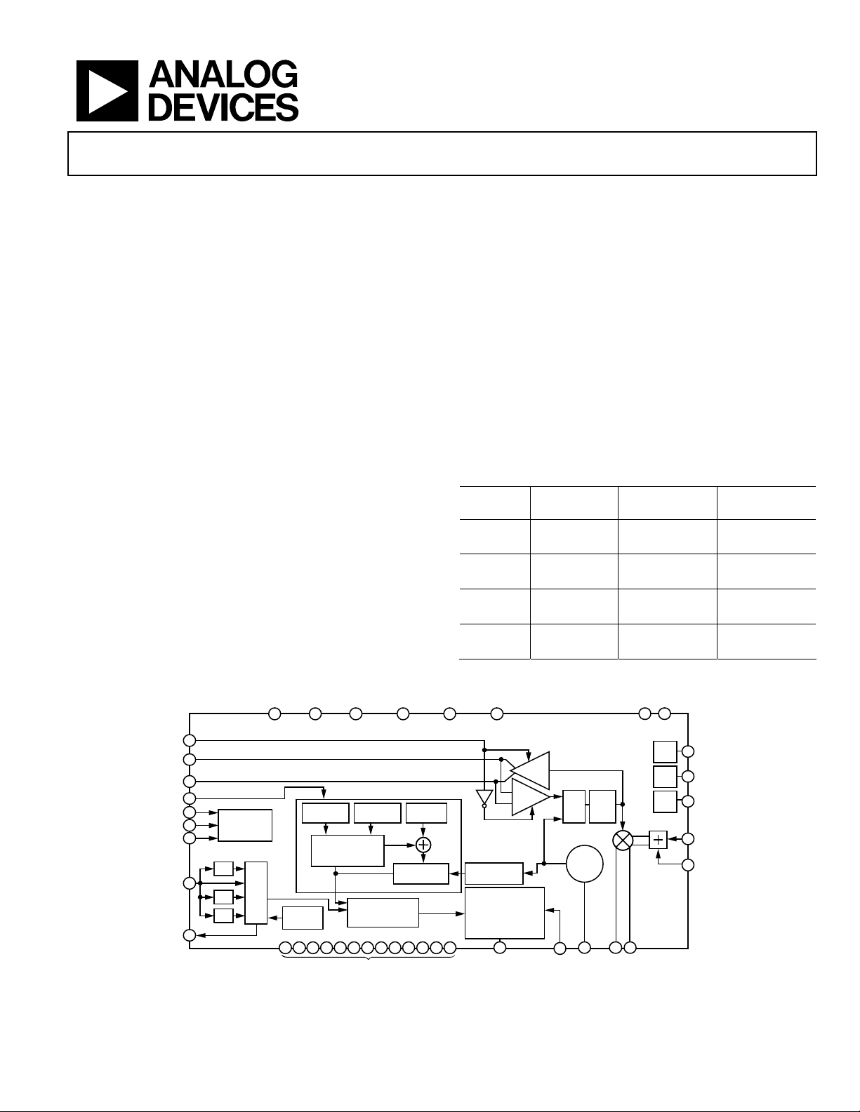
GENERAL DESCRIPTION
The ADRF6603 is a high dynamic range active mixer with
integrated phase-locked loop (PLL) and voltage controlled
oscillator (VCO). The PLL/synthesizer uses a fractional-N
PLL to generate a f
can be divided or multiplied and then applied to the PLL phase
frequency detector (PFD).
LODRV_EN
Rev. A
Information furnished by Analog Devices is believed to be accurate and reliable. However, no
responsibility is assumed by Analog Devices for its use, nor for any infringements of patents or other
rights of third parties that may result from its use. Specifications subject to change without notice. No
license is granted by implication or otherwise under any patent or patent rights of Analog Devices.
Trademarks and registered trademarks are the property of their respective owners.
input to the mixer. The reference input
LO
CC1
36
LON
37
38
LOP
PLL_EN
DATA
CLK
REF_IN
MUXOUT
16
12
13
14
LE
6
8
SPI
INTERFACE
×2
MUX
÷2
÷4
FRACTION
TEMP
SENSOR
7 11 15 20 21 23 24 25 28 30 31 35
FUNCTIONAL BLOCK DIAGRAM
CC2VCC_LOVCC_MIXVCC_V2IVCC_LO
PHASE
INTEGER
N COUNTER
21 TO 123
MODULUS
REG
THIRD-ORDER
FRACTIONAL
INTERPOLATOR
–
+
FREQUENCY
DETECTOR
GND
REG
Figure 1.
ADRF6603
The PLL can support input reference frequencies from 12 MHz
to 160 MHz. The PFD output controls a charge pump whose
output drives an off-chip loop filter.
The loop filter output is then applied to an integrated VCO. The
VCO output at 2 × f
programmable PLL divider. The programmable PLL divider is
controlled by a sigma-delta (Σ-) modulator (SDM). The modulus
of the SDM can be programmed from 1 to 2047.
The active mixer converts the single-ended 50 RF input to
a 200 Ω differential IF output. The IF output can operate up
to 500 MHz.
The ADRF6603 is fabricated using an advanced silicon-germanium
BiCMOS process. It is available in a 40-lead, RoHS-compliant,
6 mm × 6 mm LFCSP with an exposed paddle. Performance is
specified over the −40°C to +85°C temperature range.
Table 1.
Internal LO
Part No.
Range
ADRF6601 750 MHz 300 MHz 450 MHz
1160 MHz 2500 MHz 1600 MHz
ADRF6602 1550 MHz 1000 MHz 1350 MHz
2150 MHz 3100 MHz 2750 MHz
ADRF6603 2100 MHz 1100 MHz 1450 MHz
2600 MHz 3200 MHz 2850 MHz
ADRF6604 2500 MHz 1200 MHz 1600 MHz
2900 MHz 3600 MHz 3200 MHz
2717101 22
34
BUFFER
BUFFER
PRESCALER
÷2
CHARGE PUMP
250µA,
500µA (DEFAULT),
750µA,
1000µA
54
R
SET
One Technology Way, P.O. Box 9106, Norwood, MA 02062-9106, U.S.A.
Tel: 781.329.4700 www.analog.com
Fax: 781.461.3113 ©2010 Analog Devices, Inc. All rights reserved.
is applied to an LO divider, as well as to a
LO
±3 dB RF
Balun Range
ADRF6603
INTERNAL L O RANGE
2100MHz TO 2600 M Hz
DIV
2:1
BY
MUX
2, 1
VCO
CORE
3
CP VTUNE
IFP
191839
IFN
NC
32 33
3.3V
LDO
2.5V
LDO
VCO
LDO
NC
IN
2
9
40
26
29
±1 dB RFIN
Balun Range
DECL3P3
DECL2P5
DECLVCO
RF
IN
IP3SET
08547-001
Page 2

ADRF6603
TABLE OF CONTENTS
Features .............................................................................................. 1
Applications ....................................................................................... 1
General Description ......................................................................... 1
Functional Block Diagram .............................................................. 1
Revision History ............................................................................... 2
Specifications ..................................................................................... 3
RF Specifications .......................................................................... 3
Synthesizer/PLL Specifications ................................................... 4
Logic Input and Power Specifications ....................................... 4
Timing Characteristics ................................................................ 5
Absolute Maximum Ratings ............................................................ 6
ESD Caution .................................................................................. 6
Pin Configuration and Function Descriptions ............................. 7
Typical Performance Characteristics ............................................. 9
RF Frequency Sweep .................................................................... 9
IF Frequency Sweep ................................................................... 10
Spurious Performance................................................................ 15
Register Structure ........................................................................... 16
Register 0—Integer Divide Control (Default: 0x0001C0)..... 16
Register 1—Modulus Divide Control (Default: 0x003001) .. 16
Register 2—Fractional Divide Control
(Default: 0x001802) .................................................................... 17
Register 3—Σ-Δ Modulator Dither Control
(Default: 0x10000B) ................................................................... 17
Register 4—PLL Charge Pump, PFD, and Reference Path
Control (Default: 0x0AA7E4) ................................................... 18
Register 5—PLL Enable and LO Path Control
(Default: 0x0000E5) ................................................................... 19
Register 6—VCO Control and VCO Enable
(Default: 0x1E2106) ................................................................... 19
Register 7—Mixer Bias Enable and External VCO Enable
(Default: 0x000007) .................................................................... 19
Theory of Operation ...................................................................... 20
Programming the ADRF6603 ................................................... 20
Initialization Sequence .............................................................. 20
LO Selection Logic ..................................................................... 21
Applications Information .............................................................. 22
Basic Connections for Operation ............................................. 22
AC Test Fixture ............................................................................... 23
Evaluation Board ............................................................................ 24
Evaluation Board Control Software ......................................... 24
Schematic and Artwork ............................................................. 26
Evaluation Board Configuration Options ............................... 28
Outline Dimensions ....................................................................... 29
Ordering Guide .......................................................................... 29
REVISION HISTORY
11/10—Rev. 0 to Rev. A
Changes to Features and General Description ............................. 1
Changes to Table 1 ............................................................................ 1
Changes to Table 2 ............................................................................ 3
Changes to Table 3 and Table 4 ....................................................... 4
Changes to Table 6 ............................................................................ 6
Change to Table 7, Pin 36 Description .......................................... 8
Changes to Typical Performance Characteristics Section ........... 9
Added Spurious Performance Section ......................................... 15
Changes to Programming the ADRF6603 Section .................... 20
Changes to Figure 46 ...................................................................... 22
Added AC Test Fixture Section and Figure 47;
Renumbered Sequentially ............................................................. 23
Changes to Evaluation Board Control Software Section;
Changes to Figure 48 ...................................................................... 24
Changes to Figure 49 ...................................................................... 25
Changes to Figure 50 ...................................................................... 26
1/10—Revision 0: Initial Version
Rev. A | Page 2 of 32
Page 3

ADRF6603
SPECIFICATIONS
RF SPECIFICATIONS
VS = 5 V; ambient temperature (TA) = 25°C; f
using CDAC (0x1) and IP3SET (3.3 V), unless otherwise noted.
Table 2.
Parameter Test Conditions/Comments Min Typ Max Unit
INTERNAL LO FREQUENCY RANGE 2100 2600 MHz
RF INPUT FREQUENCY RANGE ±3 dB RF input range 1100 3200 MHz
RF INPUT AT 2140 MHz
Input Return Loss Relative to 50 Ω (can be improved with external match) <(−20) dB
Input P1dB 14.9 dBm
Second-Order Intercept (IIP2) −5 dBm each tone (10 MHz spacing between tones) 55.3 dBm
Third-Order Intercept (IIP3) −5 dBm each tone (10 MHz spacing between tones) 29.3 dBm
Single-Side Band Noise Figure IP3SET = 3.3 V 15.6 dB
IP3SET = open 14.4 dB
LO-to-IF Leakage At 1× LO frequency, 50 Ω termination at the RF port −43 dBm
RF INPUT AT 2400 MHz
Input Return Loss Relative to 50 Ω (can be improved with external match) −16 dB
Input P1dB 14.9 dBm
Second-Order Intercept (IIP2) −5 dBm each tone (10 MHz spacing between tones) 55.1 dBm
Third-Order Intercept (IIP3) −5 dBm each tone (10 MHz spacing between tones) 28.6 dBm
Single-Side Band Noise Figure IP3SET = 3.3 V 15.8 dB
IP3SET = open 14.2 dB
LO-to-IF Leakage At 1× LO frequency, 50 Ω termination at the RF port −43 dBm
RF INPUT AT 2650 MHz
Input Return Loss Relative to 50 Ω (can be improved with external match) −11 dB
Input P1dB 14.7 dBm
Second-Order Intercept (IIP2) −5 dBm each tone (10 MHz spacing between tones) 52.1 dBm
Third-Order Intercept (IIP3) −5 dBm each tone (10 MHz spacing between tones) 28.1 dBm
Single-Side Band Noise Figure IP3SET = 3.3 V 15.8 dB
IP3SET = open 14.5 dB
LO-to-IF Leakage At 1× LO frequency, 50 Ω termination at the RF port −44 dBm
IF OUTPUT
Voltage Conversion Gain Differential 200 Ω load 6.7 dB
IF Bandwidth Small signal 3 dB bandwidth 500 MHz
Output Common-Mode Voltage External pull-up balun or inductors required 5 V
Gain Flatness Over frequency range, any 5 MHz/50 MHz 0.2/1.0 dB
Gain Variation Over full temperature range 1.2 dB
Output Swing Differential 200 Ω load 2 V p-p
Differential Output Return Loss Measured through 4:1 balun −15 dB
LO INPUT/OUTPUT (LOP, LON) Externally applied 1× LO input, internal PLL disabled
Frequency Range 250 6000 MHz
Output Level (LO as Output) 1× LO into a 50 Ω load, LO output buffer enabled −7 dBm
Input Level (LO as Input) −6 0 +6 dBm
Input Impedance 50 Ω
= 153.6 MHz; f
REF
= 38.4 MHz; high-side LO injection; fIF = 140 MHz; IIP3 optimized
PFD
Rev. A | Page 3 of 32
Page 4

ADRF6603
SYNTHESIZER/PLL SPECIFICATIONS
VS = 5 V; ambient temperature (TA) = 25°C; f
= 140 MHz; IIP3 optimized using CDAC (0x1) and IP3SET (3.3 V), unless otherwise noted.
f
IF
Table 3.
Parameter Test Conditions/Comments Min Typ Max Unit
SYNTHESIZER SPECIFICATIONS Synthesizer specifications referenced to 1× LO
Frequency Range Internally generated LO 2100 2600 MHz
Figure of Merit1 P
Reference Spurs f
f
f
PFD
PFD
PFD
>f
PHASE NOISE fLO = 2100 MHz to 2600 MHz, f
1 kHz to 10 kHz offset −88 dBc/Hz
100 kHz offset −99.5 dBc/Hz
500 kHz offset −120 dBc/Hz
1 MHz offset −128 dBc/Hz
5 MHz offset −142 dBc/Hz
10 MHz offset −148 dBc/Hz
20 MHz offset −150 dBc/Hz
Integrated Phase Noise 1 kHz to 40 MHz integration bandwidth 0.42
PFD Frequency 20 40 MHz
REFERENCE CHARACTERISTICS REF_IN, MUXOUT pins
REF_IN Input Frequency 12 160 MHz
REF_IN Input Capacitance 4 pF
MUXOUT Output Level VOL (lock detect output selected) 0.25 V
V
MUXOUT Duty Cycle 50 %
CHARGE PUMP
Pump Current Programmable to 250 μA, 500 μA, 750 μA, 1 mA 500 μA
Output Compliance Range 1 2.8 V
1
The figure of merit (FOM) is computed as phase noise (dBc/Hz) – 10Log10(f
power = 10 dBm (500 V/μs slew rate) with a 40 MHz f
and f
REF
= 153.6 MHz; f
REF
= 0 dBm −222 dBc/Hz/Hz
REF_IN
power = 4 dBm; f
REF
= 38.4 MHz; high-side LO injection;
PFD
= 38.4 MHz
/4 −107 dBc
−82 dBc
−85 dBc
PFD
= 38.4 MHz
PFD
°rms
(lock detect output selected) 2.7 V
OH
) – 20Log10(fLO/f
. The FOM was computed at 50 kHz offset.
PFD
PFD
). The FOM was measured across the full LO range, with f
PFD
= 80 MHz,
REF
LOGIC INPUT AND POWER SPECIFICATIONS
VS = 5 V; ambient temperature (TA) = 25°C; f
using CDAC (0x1) and IP3SET (3.3 V), unless otherwise noted.
Table 4.
Parameter Test Conditions/Comments Min Typ Max Unit
LOGIC INPUTS CLK, DATA, LE
Input High Voltage, V
Input Low Voltage, V
Input Current, I
1.4 3.3 V
INH
0 0.7 V
INL
0.1 μA
INH/IINL
Input Capacitance, CIN 5 pF
POWER SUPPLIES VCC1, VCC2, VCC_LO, VCC_MIX, and VCC_V2I pins
Voltage Range 4.75 5 5.25 V
Supply Current PLL only 97 mA
External LO mode (internal PLL disabled, LO output buffer off, IP3SET pin = 3.3 V) 164 mA
Internal LO mode (internal PLL enabled, IP3SET pin = 3.3 V, LO output buffer on) 274 mA
Internal LO mode (internal PLL enabled, IP3SET pin = 3.3 V, LO output buffer off) 261 mA
Power-down mode 30 mA
= 153.6 MHz; f
REF
= 38.4 MHz; high-side LO injection; fIF = 140 MHz; IIP3 optimized
PFD
Rev. A | Page 4 of 32
Page 5
ADRF6603
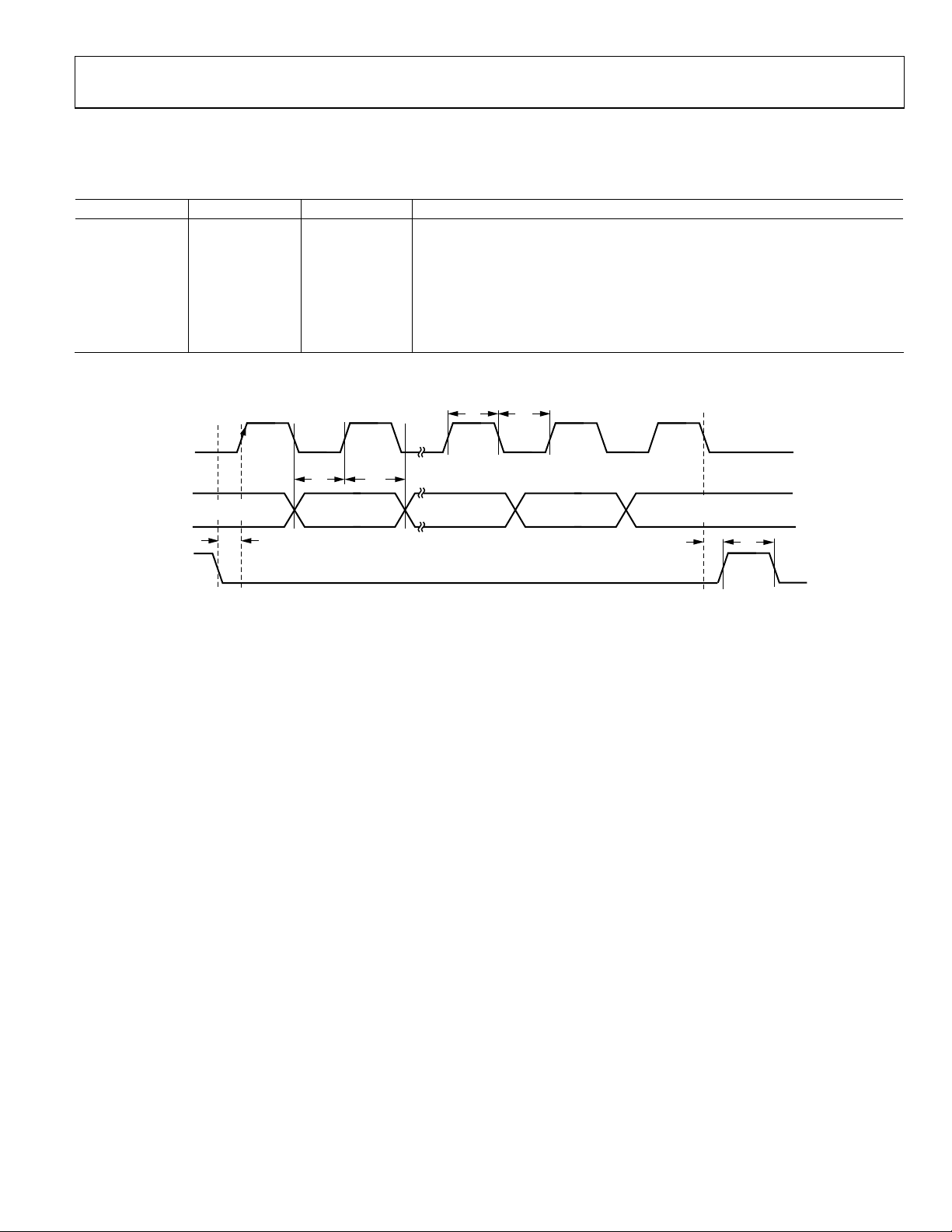
TIMING CHARACTERISTICS
VCC2 = 5 V ± 5%.
Table 5.
Parameter Limit Unit Description
t1 20 ns min LE setup time
t2 10 ns min DATA-to-CLK setup time
t3 10 ns min DATA-to-CLK hold time
t4 25 ns min CLK high duration
t5 25 ns min CLK low duration
t6 10 ns min CLK-to-LE setup time
t7 20 ns min LE pulse width
Timing Diagram
CLK
t
4
t
5
DATA
DB23 (MSB) DB22
t
1
LE
t
2
t
3
DB2 DB1
(CONTROL BIT C2)(CONTROL BIT C3)
DB0 (LSB)
(CONTROLBIT C1)
t
6
t
7
08547-002
Figure 2. Timing Diagram
Rev. A | Page 5 of 32
Page 6
ADRF6603
ABSOLUTE MAXIMUM RATINGS
Table 6.
Parameter Rating
Supply Voltage, VCC1, VCC2, VCC_LO,
VCC_MIX, VCC_V2I
Digital I/O, CLK, DATA, LE, LODRV_EN,
PLL_EN
VTUNE 0 V to 3.3 V
IFP, IFN −0.3 V to VCC_V2I + 0.3 V
RFIN 16 dBm
LOP, LON, REF_IN 13 dBm
θJA (Exposed Paddle Soldered Down) 35°C/W
Maximum Junction Temperature 150°C
Operating Temperature Range −40°C to +85°C
Storage Temperature Range −65°C to +150°C
−0.5 V to +5.5 V
−0.3 V to +3.6 V
Stresses above those listed under Absolute Maximum Ratings
may cause permanent damage to the device. This is a stress
rating only; functional operation of the device at these or any
other conditions above those indicated in the operational
section of this specification is not implied. Exposure to absolute
maximum rating conditions for extended periods may affect
device reliability.
ESD CAUTION
Rev. A | Page 6 of 32
Page 7
ADRF6603
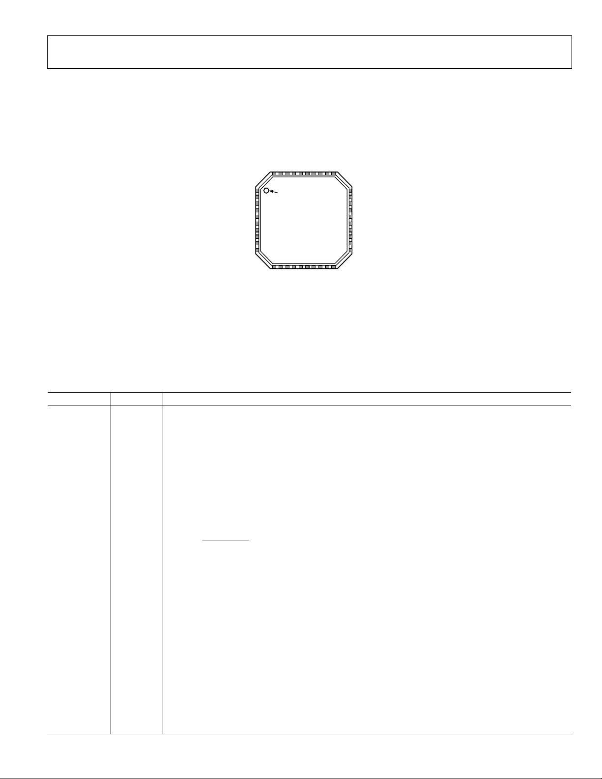
PIN CONFIGURATION AND FUNCTION DESCRIPTIONS
ODRV_EN
NC
VCC_LO
GND
L
LON
DECLVCO
LOP
VTUNE
37
38
39
40
NC
GND
32
31
33
34
35
36
1VCC1
2DECL3P3
3CP
GND
4
R
5
SET
REF_IN
MUXOUT
DECL2P5
NOTES
1. NC = NO CONNECT.
2. THE EXPOSED PADDLE SHOULD BE SOLDERED TO A
LOW IMPEDANCE GROUND PLANE.
GND
VCC2
6
7
8
9
10
PIN 1
INDICATOR
ADRF6603
TOP VIEW
(Not to Scale)
4
11
13
12
1
15
16
LE
CLK
GND
GND
DATA
PLL_EN
30 GND
29 IP3SET
28 GND
27 VCC_V2I
RF
26
IN
25
GND
24 GND
23 GND
22 VCC_MIX
21
GND
20
19
18
17
IFP
IFN
GND
VCC_LO
08547-003
Figure 3. Pin Configuration
Table 7. Pin Function Descriptions
Pin No. Mnemonic Description
1 VCC1
Power Supply for the 3.3 V LDO. Power supply voltage range is 4.75 V to 5.25 V. Each power supply pin
should be decoupled with a 100 pF capacitor and a 0.1 μF capacitor located close to the pin.
2 DECL3P3 Decoupling Node for 3.3 V LDO. Connect a 0.1 μF capacitor between this pin and ground.
3 CP Charge Pump Output Pin. Connect to VTUNE through the loop filter.
4, 7, 11, 15, 20,
GND Ground. Connect these pins to a low impedance ground plane.
21, 23, 24, 25,
28, 30, 31, 35
5 R
SET
Charge Pump Current. The nominal charge pump current can be set to 250 μA, 500 μA, 750 μA, or 1 mA using
Bit DB11 and Bit DB10 in Register 4 and by setting Bit DB18 in Register 4 to 0 (internal reference current). In
this mode, no external R
is required. If Bit DB18 is set to 1, the four nominal charge pump currents (I
SET
can be externally adjusted according to the following equation:
=
R
SET
6 REF_IN
Reference Input. Nominal input level is 1 V p-p. Input range is 12 MHz to 160 MHz. This pin is internally dc-
⎛
⎜
⎜
⎝
I
NOMINAL
⎞
CP
⎟
⎟
⎠
37.8
−
×
I
4.217
biased and should be ac-coupled.
8 MUXOUT
Multiplexer Output. This output can be programmed to provide the reference output signal or the lock detect
signal. The output is selected by programming the appropriate register.
9 DECL2P5 Decoupling Node for 2.5 V LDO. Connect a 0.1 μF capacitor between this pin and ground.
10 VCC2
Power Supply for the 2.5 V LDO. Power supply voltage range is 4.75 V to 5.25 V. Each power supply pin
should be decoupled with a 100 pF capacitor and a 0.1 μF capacitor located close to the pin.
12 DATA Serial Data Input. The serial data input is loaded MSB first; the three LSBs are the control bits.
13 CLK
Serial Clock Input. The serial clock input is used to clock in the serial data to the registers. The data is latched
into the 24-bit shift register on the CLK rising edge. Maximum clock frequency is 20 MHz.
14 LE
Load Enable. When the LE input pin goes high, the data stored in the shift registers is loaded into one of the
eight registers. The relevant latch is selected by the three control bits of the 24-bit word.
16 PLL_EN
PLL Enable. Switch between internal PLL and external LO input. When this pin is logic high, the mixer LO is
automatically switched to the internal PLL and the internal PLL is powered up. When this pin is logic low, the
internal PLL is powered down and the external LO input is routed to the mixer LO inputs. The SPI can also be
used to switch modes.
Rev. A | Page 7 of 32
NOMINAL
)
Page 8

ADRF6603
Pin No. Mnemonic Description
17, 34 VCC_LO
18, 19 IFP, IFN Mixer IF Outputs. These outputs should be pulled to VCC with RF chokes.
22 VCC_MIX
26 RFIN RF Input (Single-Ended, 50 Ω).
27 VCC_V2I
29 IP3SET Connect a resistor from this pin to a 5 V supply to adjust IIP3. Normally leave open.
32, 33 NC No Connection.
36 LODRV_EN
37, 38 LON, LOP
39 VTUNE
40 DECLVCO Decoupling Node for VCO LDO. Connect a 100 pF capacitor and a 10 μF capacitor between this pin and ground.
EPAD Exposed Paddle. The exposed paddle should be soldered to a low impedance ground plane.
Power Supply. Power supply voltage range is 4.75 V to 5.25 V. Each power supply pin should be decoupled
with a 100 pF capacitor and a 0.1 μF capacitor located close to the pin.
Power Supply. Power supply voltage range is 4.75 V to 5.25 V. Each power supply pin should be decoupled
with a 100 pF capacitor and a 0.1 μF capacitor located close to the pin.
Power Supply. Power supply voltage range is 4.75 V to 5.25 V. Each power supply pin should be decoupled
with a 100 pF capacitor and a 0.1 μF capacitor located close to the pin.
LO Driver Enable. Together with Pin 16 (PLL_EN), this digital input pin determines whether the LOP and LON
pins operate as inputs or outputs. LOP and LON become inputs if the PLL_EN pin is low or if the PLL_EN pin
is set high with the PLEN bit (DB6 in Register 5) set to 0. LOP and LON become outputs if either the LODRV_EN
pin or the LDRV bit (DB3 in Register 5) is set to 1 while the PLL_EN pin is set high. External LO drive frequency
must be 1× LO. This pin has an internal 100 kΩ pull down resistor.
Local Oscillator Input/Output. The internally generated 1× LO is available on these pins. When internal LO
generation is disabled, an external 1× LO can be applied to these pins.
VCO Control Voltage Input. This pin is driven by the output of the loop filter. Nominal input voltage range on
this pin is 1.5 V to 2.5 V.
Rev. A | Page 8 of 32
Page 9
ADRF6603
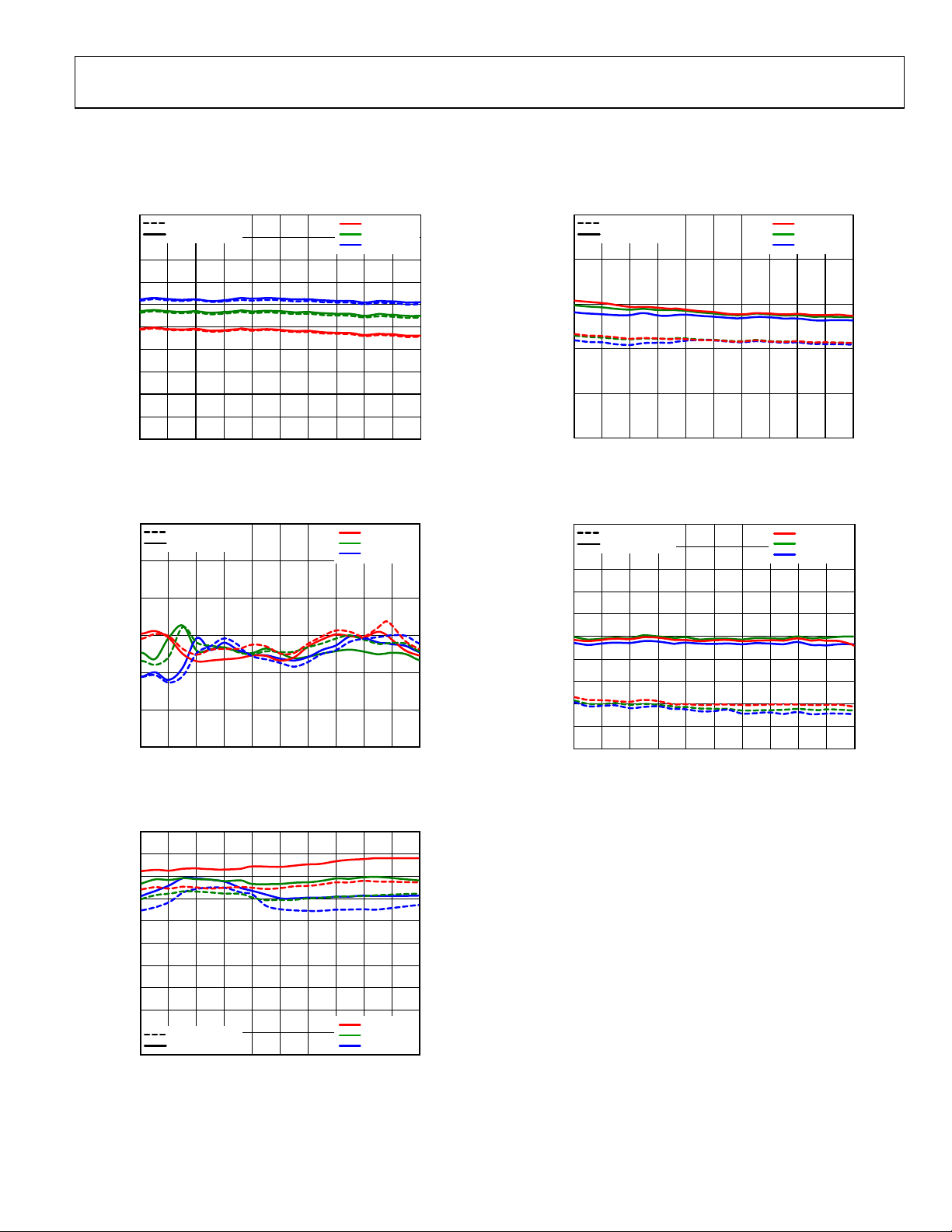
TYPICAL PERFORMANCE CHARACTERISTICS
RF FREQUENCY SWEEP
CDAC = 0x1, internally generated high-side LO, RFIN = −5 dBm, fIF = 140 MHz, unless otherwise noted.
5
IP3SET = OPEN
IP3SET = 3.3V
4
3
2
1
0
GAIN (dB)
–1
–2
–3
–4
–5
1960 2010 2060 2110 2160 2210 2260 2310 2360 2410 2460
RF FREQUENCY (MHz)
TA = +85°C
TA = +25°C
TA = –40°C
Figure 4. Gain vs. RF Frequency
08547-104
40
IP3SET = OPEN
IP3SET = 3.3V
35
30
25
INPUT IP3 (dBm)
20
15
1960 2010 2060 2110 2160 2210 2260 2310 2360 2410 2460
RF FREQUENCY ( MHz)
TA = +85°C
TA = +25°C
TA = –40°C
Figure 7. Input IP3 vs. RF Frequency
08547-107
90
IP3SET = OPEN
IP3SET = 3.3V
80
70
60
INPUT IP2 (dBm)
50
40
30
1960 2010 2060 2110 2160 2210 2260 2310 2360 2410 2460
RF FREQUENCY ( MHz)
TA = +85°C
TA = +25°C
TA = –40°C
Figure 5. Input IP2 vs. RF Frequency
20
18
16
14
12
10
8
NOISE FIGURE (dB)
6
4
2
IP3SET = OPEN
IP3SET = 3.3V
0
1960 2010 2060 2110 2160 2210 2260 2310 2360 2410 2460
RF FREQUENCY ( MHz)
TA = +85°C
TA = +25°C
TA = –40°C
Figure 6. Noise Figure vs. RF Frequency
20
IP3SET = OPEN
IP3SET = 3.3V
19
18
17
16
15
14
INPUT P1dB (dBm)
13
12
11
10
1960 2010 2060 2110 2160 2210 2260 2310 2360 2410 2460
08547-105
RF FREQUENCY (MHz)
TA = +85°C
TA = +25°C
TA = –40°C
08547-108
Figure 8. Input P1dB vs. RF Frequency
08547-106
Rev. A | Page 9 of 32
Page 10
ADRF6603
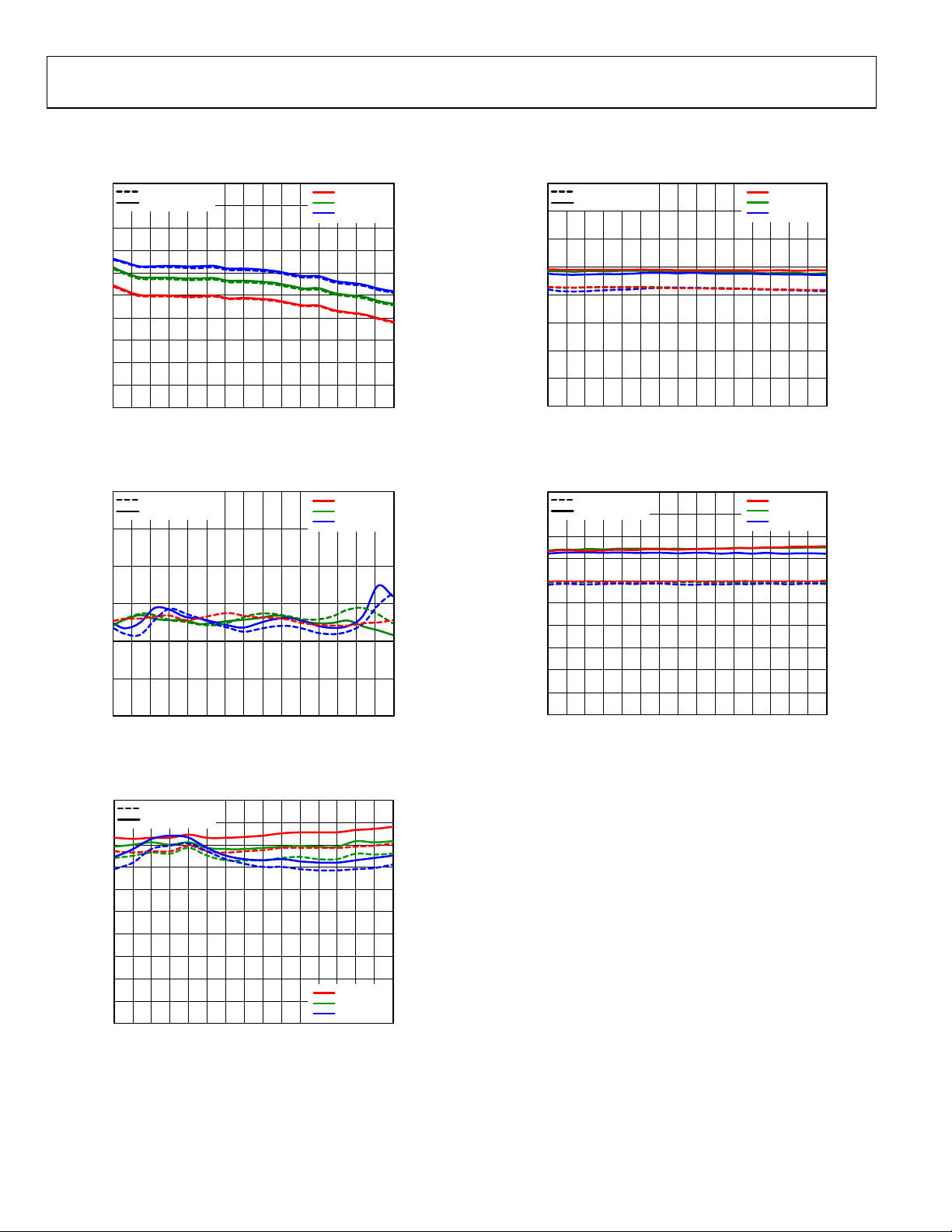
IF FREQUENCY SWEEP
CDAC = 0x1, internally generated swept low-side LO, fRF = 1960 MHz, RFIN = −5 dBm, unless otherwise noted.
5
IP3SET = OPEN
IP3SET = 3.3V
4
3
2
1
0
GAIN (dB)
–1
–2
–3
–4
–5
25 50 75 100 125 150 175 200 225 250 275 300 325 350 375 400
IF FR E QUENCY (MHz)
Figure 9. Gain vs. IF Frequency
TA = +85°C
TA = +25°C
TA = –40°C
08547-109
45
IP3SET = OPEN
IP3SET = 3.3V
40
35
30
25
20
INPUT IP3 (dBm)
15
10
5
25 4003753503253002752502252001751501257550 100
IF FREQ UE NCY ( MHz)
Figure 12. Input IP3 vs. IF Frequency, RF
TA = +85°C
TA = +25°C
TA = –40°C
= −5 dBm
IN
08547-112
90
IP3SET = OPEN
IP3SET = 3.3V
80
70
60
INPUT IP2 (dBm)
50
40
30
25 50 75 100 125 150 175 200 225 250 275 300 325 350 375 400
Figure 10. Input IP2 vs. IF Frequency, RF
20
IP3SET = OPEN
IP3SET = 3.3V
18
16
14
12
10
8
NOISE FI GURE (dB)
6
4
2
0
25 4003753503253002752502252001751501257550 100
IF FR E QUENCY (MHz)
IF FREQ UE NCY ( MHz)
= −5 dBm
IN
Figure 11. Noise Figure vs. IF Frequency
TA = +85°C
TA = +25°C
TA = –40°C
TA = +85°C
TA = +25°C
TA = –40°C
20
IP3SET = OPEN
IP3SET = 3.3V
18
16
14
12
10
8
INPUT P1dB (dBm)
6
4
2
0
25 4003753503253002752502252001751501257550 100
08547-110
IF FREQ UE NCY ( MHz)
TA = +85°C
TA = +25°C
TA = –40°C
08547-113
Figure 13. Input P1dB vs. IF Frequency
08547-111
Rev. A | Page 10 of 32
Page 11

ADRF6603
–
0
IP3SET = OPEN
–5
IP3SET = 3.3V
–10
–15
–20
–25
–30
–35
–40
–45
LO-TO-IF FEEDTHROUGH (dBm )
–50
–55
–60
2100 2150 2200 2250 2300 2350 2400 2450 2500 2550 2600
LO FREQUENCY (MHz)
TA = +85°C
TA = +25°C
TA = –40°C
Figure 14. LO-to-IF Feedthrough vs. LO Frequency,
LO Output Turned Off, CDAC = 0x0
20
–25
–30
–35
–40
–45
–50
–55
–60
–65
–70
LO-TO-RF L E A KAGE (dBm)
–75
–80
–85
–90
2100 26002500240023002200
IP3SET = OPEN
IP3SET = 3.3V
LO FREQUENCY (MHz)
TA = +85°C
TA = +25°C
TA = –40°C
Figure 15. LO-to-RF Leakage vs. LO Frequency, LO Output Turned Off
08547-114
08547-115
0
–2
–4
–6
–8
–10
–12
RETURN LOSS ( dB)
–14
–16
–18
–20
1900 280027002600250024002300220021002000
LO FREQUENCY (MHz)
08547-117
Figure 17. LO Input Return Loss vs. LO Frequency (Including TC1-1-13 Balun)
RESISTANCE (Ω)
350
300
250
200
150
100
50
0
50 500450400350300250200150100
RESISTANCE
CAPACITANCE
IF FREQ UE NC Y (M Hz )
3.5
3.0
2.5
2.0
1.5
1.0
0.5
0
CAPACITANCE (pF)
Figure 18. IF Differential Output Impedance (R Parallel C Equivalent)
08547-118
RETURN LOSS ( dB)
0
–5
–10
–15
–20
–25
–30
–35
–40
–45
1900 280027002600250024002300220021002000
RF FREQUENCY ( MHz )
Figure 16. RF Input Return Loss vs. RF Frequency
08547-116
Rev. A | Page 11 of 32
35
IP3SET = OPEN
IP3SET = 3.3V
30
25
20
NOISE FIGURE (dB)
15
10
–60 –50 –40 –30 –20 –10 0
CW BLOCKER LEVEL (dBm)
Figure 19. SSB Noise Figure vs. 5 MHz Offset Blocker Level,
LO Frequency = 2105 MHz, RF Frequency = 1965 MHz
08547-119
Page 12

ADRF6603
–
0
RF-TO- IF ISOLATION (dB)
–5
–10
–15
–20
–25
–30
–35
–40
–45
–50
–55
–60
1900 280027002600250024002300220021002000
IP3SET = OPEN
IP3SET = 3.3V
LO FREQUENCY (MHz)
TA = +85°C
TA = +25°C
TA = –40°C
Figure 20. RF-to-IF Isolation vs. RF Frequency, High-Side LO, IF = 140 MHz,
LO Output Turned Off
2
IP3SET = OPEN
IP3SET = 3.3V
–3
–4
–5
–6
–7
–8
–9
–10
LO OUTP UT AMPLITUDE (dBm)
–11
–12
2100 2150 2200 2250 2300 2350 2400 2450 2500 2550 2600
LO FREQUENCY (MHz)
TA = +85°C
TA = +25°C
TA = –40°C
Figure 21. LO Output Amplitude vs. LO Frequency
08547-120
08547-121
5.0
4.5
4.0
3.5
3.0
2.5
2.0
VTUNE VOL TAGE (V)
1.5
1.0
0.5
0
2100 2200 2300 2400 2500 2600
LO FREQUENCY (MHz)
TA = +85°C
TA = +25°C
TA = –40°C
Figure 23. VTUNE vs. LO Frequency
350
300
250
200
SUPPLY CURRENT (mA)
150
100
2100 2600255025002450240023502300225022002150
IP3SET = OPEN
IP3SET = 3.3V
LO FREQUENCY (MHz)
TA = +85°C
TA = +25°C
TA = –40°C
Figure 24. Supply Current vs. LO Frequency
08547-123
08547-124
20
15
10
5
0
–5
–10
–15
FREQUENCY DEV IATION FROM 2140MHz ( MHz)
–20
0 50 100 150 200 250
TIME (µs)
Figure 22. Frequency Deviation from 2140 MHz vs Time
(Demonstrates LO Frequency Settling Time from 2150 MHz to 2140 MHz)
08547-122
Rev. A | Page 12 of 32
2.5
2.4
2.3
2.2
2.1
2.0
1.9
1.8
1.7
1.6
1.5
VPTAT VOLTAGE (V)
1.4
1.3
1.2
1.1
1.0
IP3SET = OPEN
IP3SET = 3.3V
–55 –35 –15 5 25 45 65 85 105
TEMPERATURE (°C)
Figure 25. VPTAT Voltage vs. Temperature (IP3SET = Optimized, Open)
08547-125
Page 13

ADRF6603
Complementary cumulative distribution function (CCDF), fRF = 2140 MHz, fIF = 140 MHz.
100
DISTRI BU T ION PERCENTAGE (%)
IP3SET = OPEN
IP3SET = 3.3V
90
80
70
60
50
40
30
20
10
TA = +85°C
TA = +25°C
TA = –40°C
0
–1.0 –0.5 0 0.5 1.0 1.5 2.0
GAIN (dB)
Figure 26. Gain
08547-126
100
DISTRIBUTION PERCENTAGE (%)
IP3SET = OPEN
IP3SET = 3.3V
90
80
70
60
50
40
30
20
10
0
20 22 24 26 28 30 32 34 36
INPUT IP3 (dBm)
Figure 29. Input IP3
TA = +85°C
TA = +25°C
TA = –40°C
08547-129
100
DISTRIBUTION PERCENTAGE (%)
IP3SET = OPEN
IP3SET = 3.3V
90
TA = +85°C
TA = +25°C
80
TA = –40°C
70
60
50
40
30
20
10
0
40 45 50 55 60 65 70
INPUT IP2 (dBm)
Figure 27. Input IP2
100
IP3SET = OPEN
90
80
70
60
50
40
30
20
DISTRIBUTION PERCENTAGE (%)
10
0
11 12 13 14 15 16 17 18
NOISE FI GURE (dB)
Figure 28. Noise Figure
TA = +85°C
TA = +25°C
TA = –40°C
100
90
80
70
60
50
40
30
20
DISTRIBUTION PERCENTAGE (%)
10
0
9 10111213141516 1817
08547-127
INPUT P1dB (dBm)
IP3SET = OPEN
IP3SET = 3.3V
TA = +85°C
TA = +25°C
TA = –40°C
08547-130
Figure 30. Input P1dB
100
DISTRIBUT ION PERCENT AGE (%)
08547-128
IP3SET = OPEN
IP3SET = 3.3V
90
80
70
60
50
40
30
20
10
0
–55 –53 –51 –49 –47 –45 –43 –41 –39 –37 –35
LO FEEDTHROUGH (d Bm)
TA = +85°C
TA = +25°C
TA = –40°C
08547-131
Figure 31. LO Feedthrough to IF, LO Output Turned Off
Rev. A | Page 13 of 32
Page 14

ADRF6603
–
–
–
–
–
Measured at IF output, CDAC = 0x1, IP3SET = open, internally generated high-side LO, f
RF
= −5 dBm, fIF = 140 MHz, unless otherwise noted. Phase noise measurements made at LO output, unless otherwise noted.
IN
80
LO FREQUENCY = 2595.2MHz
–90
–100
–110
–120
LO FREQUENCY = 2115.2MHz
–130
PHASE NOISE (dBc/Hz)
–140
–150
–160
1k 10k 100k 1M 10M 100M
OFFSET FREQUENCY (Hz)
Figure 32. Phase Noise vs. Offset Frequency
TA = +85°C
TA = +25°C
TA = –40°C
08547-132
INTEGRATED PHASE NOISE (°rms)
1.0
0.9
0.8
0.7
0.6
0.5
0.4
0.3
0.2
0.1
0
2100 2600255025002450240023502300225022002150
= 153.6 MHz, f
REF
LO FREQUENCY (MHz)
= 38.4 MHz,
PFD
TA = +85°C
TA = +25°C
TA = –40°C
Figure 35. Integrated Phase Noise vs. LO Frequency
08547-135
75
2× PFD FREQUENCY
–80
–85
–90
–95
SPURRS LEVEL (dBc)
–100
–105
–110
4× PFD FREQUENCY
2100 2150 2200 2250 2300 2350 2400 2450 2500 2550 2600
LO FREQUENCY (MHz)
TA = +85°C
TA = +25°C
TA = –40°C
Figure 33. PLL Reference Spurs vs. LO Frequency (2× PFD and 4× PFD)
75
3× PFD FREQUENCY
–80
–85
–90
–95
SPURRS LEVEL (dBc)
–100
–105
–110
1× PFD FREQUENCY
0.25× PFD FREQUENCY
2100 2150 2200 2250 2300 2350 2400 2450 2500 2550 2600
LO FREQUENCY (MHz)
TA = +85°C
TA = +25°C
TA = –40°C
Figure 34. PLL Reference Spurs vs. LO Frequency (0.25× PFD, 1× PFD, and 3× PFD)
80
–90
–100
–110
–120
–130
PHASE NOIS E ( dBc/Hz)
–140
–150
–160
2100 2600255025002450240023502300225022002150
08547-133
OFFSET = 1kHz
OFFSE T = 100kHz
OFFSET = 5MHz
LO FREQUENCY (MHz)
TA = +85°C
TA = +25°C
TA = –40°C
08547-136
Figure 36. Phase Noise vs. LO Frequency (1 kHz, 100 kHz, and 5 MHz Steps)
80
–90
–100
–110
–120
–130
PHASE NOISE (dBc/Hz)
–140
–150
–160
2100 2600255025002450240023502300225022002150
08547-134
OFFSE T = 10kHz
OFFSET = 1MHz
LO FREQUENCY (MHz)
TA = +85°C
TA = +25°C
TA = –40°C
08547-137
Figure 37. Phase Noise vs. LO Frequency (10 kHz, 1 MHz Steps)
Rev. A | Page 14 of 32
Page 15

ADRF6603
SPURIOUS PERFORMANCE
(N × fRF) − (M × fLO) spur measurements were made using the standard evaluation board (see the Evaluation Board section). Mixer spurious
products were measured in dB relative to the carrier (dBc) from the IF output power level. All spurious components greater than −125 dBc
are shown.
LO = 2280 MHz, RF = 2140 MHz (horizontal axis is m, vertical axis is n), and RF
0
1
2
N
3
4
5
6
7
0 1 2 3 4
−114.35 −45.19 −36.94
−20.79 0.0 −67.43 −52.11
−58.20 −61.95 −78.15 −85.93 −93.10
−71.79 −91.89 −67.46 −105.88
−107.79 −110.27 −107.87
−107.88 −112.41
−107.71
−108.62
M
LO = 2540 MHz, RF = 2400 MHz (horizontal axis is m, vertical axis is n), and RF
0 −113.65 −47.04 −36.36
1 −18.91 0.0 −65.01 −56.24
2 −59.08 −60.49 −69.27 −89.85 −94.25
N
3 −77.54 −89.56 −68.39 −109.30
4
5
6
7
0 1 2 3 4
−108.79 −110.65 −111.94
M
−108.85 −111.54
LO = 2650 MHz, RF = 2510 MHz (horizontal axis is m, vertical axis is n), and RF
0 −111.38 −46.57 −36.03
1 −17.70 0.0 −65.70 −54.37
2 −58.49 −75.49 −72.27 −71.05 −95.32
N
3 −81.35 −89.18 −68.23 −103.38
4
5
6
7
0 1 2 3 4
−106.13 −106.74 −112.72
M
−107.26 −105.45
power = 0 dBm.
IN
power = 0 dBm.
IN
−108.89
power = 0 dBm.
IN
−110.74
Rev. A | Page 15 of 32
Page 16

ADRF6603
REGISTER STRUCTURE
This section provides the register maps for the ADRF6603. The three LSBs determine the register that is programmed.
REGISTER 0—INTEGER DIVIDE CONTROL (DEFAULT: 0x0001C0)
RESERVED
DB23 DB22 DB21 DB20 DB19 DB18 DB17 DB16 DB15 DB14 DB13 DB12 DB11 DB10 DB9 DB8 DB7 DB6 DB5 DB4 DB3 DB2 DB1 DB0
0000000000000DMID6ID5ID4ID3ID2ID1ID0C3(0)C2(0)C1(0)
DM
0
1
ID6 ID5 ID4 ID3 ID2 ID1 ID0
0010101
0010110
0010111
0011000
... ... ... ... ... ... ...
... ... ... ... ... ... ...
0111000
... ... ... ... ... ... ...
... ... ... ... ... ... ...
1110111
1111000
1111001
1111010
1111011
DIVIDE
MODE
DIVIDE M ODE
FRACTIONAL (DEFAULT)
INTEGER
INTEG E R DIVIDE RAT IO CONTROL BITS
INTEGER DIVIDE RAT IO
21 (INTEGER MODE ONLY)
22 (INTEGER MODE ONLY)
23 (INTEGER MODE ONLY)
24
...
...
56 (DEFAULT)
...
...
119
120 (INTE GER MODE ONLY)
121 (INTE GER MODE ONLY)
122 (INTE GER MODE ONLY)
123 (INTE GER MODE ONLY)
Figure 38. Register 0—Integer Divide Control Register Map
08547-004
REGISTER 1—MODULUS DIVIDE CONTROL (DEFAULT: 0x003001)
DB23 DB22 DB21 DB20 DB19 DB18 DB17 DB16 DB15 DB14 DB13 DB12 DB11 DB10 DB9 DB8 DB7 DB6 DB5 DB4 DB3 DB2 DB1 DB0
RESERVED
0 0 0 0 0 0 0 0 0 0 MD10 MD9 MD8 MD7 MD6 MD5 MD4 MD3 MD2 MD1 MD0 C3(0) C2(0) C1(1)
MD10MD9MD8MD7MD6MD5MD4MD3MD2MD1MD0
0 0000000001
0 0000000010
... ... ... .. . ... ... ... ... ... ... .. .
... ... ... .. . ... ... ... ... ... ... .. .
1 1000000000
... ... ... .. . ... ... ... ... ... ... .. .
... ... ... .. . ... ... ... ... ... ... .. .
1 1111111111
Figure 39. Register 1—Modulus Divide Control Register Map
Rev. A | Page 16 of 32
MODULUS VALUE
CONTROL BITS
MODULUS VALUE
1
2
...
...
1536 (DEFAULT )
...
...
2047
8547-005
Page 17

ADRF6603
REGISTER 2—FRACTIONAL DIVIDE CONTROL (DEFAULT: 0x001802)
DB23 DB22 DB21 DB20 DB19 DB18 DB17 DB16 DB15 DB14 DB13 DB12 DB11 DB10 DB9 DB8 DB7 DB6 DB5 DB4 DB3 DB2 DB1 DB0
FRACTIONAL VALUERESERVED
0 0 0 0 0 0 0 0 0 0 FD10 FD9 FD8 FD7 FD6 FD5 FD4 FD3 FD2 FD1 FD0 C3(0) C2(1) C1(0)
CONTROL BITS
FD10FD9FD8FD7FD6FD5FD4FD3FD2FD1FD0
0 0000000000
0 0000000001
... ... ... ... ... ... ... ... ... ... ...
... ... ... ... ... ... ... ... ... ... ...
0 1100000000
... ... ... ... ... ... ... ... ... ... ...
... ... ... ... ... ... ... ... ... ... ...
FRACTIONAL VALUE MUST BE LESS THAN MO DULUS
Figure 40. Register 2—Fractional Divide Control Register Map
REGISTER 3—Σ-Δ MODULATOR DITHER CONTROL (DEFAULT: 0x10000B)
DB23 DB22 DB21 DB20 DB19 DB18 DB17 DB16 DB15 DB14 DB13 DB12 DB11 DB10 DB9 DB8 DB7 DB6 DB5 DB4 DB3 DB2 DB1 DB0
0 DITH1 DITH0 DEN DV16 DV15 DV14 DV13 DV12 DV11 DV10 DV9 DV8 DV7 DV6 DV5 DV4 DV3 DV2 DV1 DV0 C3(0) C2(1) C1(1)
DITH1 DITH0
00
01
10
11
DITHER
MAGNITUDE
DITHER MAGNITUDE
15 (DEFAULT )
7
3
1 (RECOMMENDED)
DITHER
ENABLE
DEN
0
1
DITHER RESTART VALUE CONTROL BITS
DITHER ENABLE
DISABLE
ENABLE (DEFAUL T, RECOMME NDED)
FRACTIONAL VALUE
0
1
...
...
768 (DEFAULT )
...
...
<MDR
08547-006
DV16 DV15 DV14 DV13 DV12 DV11 DV10 DV9 DV8 DV7 DV6 DV5 DV4 DV3 DV2 DV1 DV0
00000000000000001
... ... ... ... ... ... ... ... ... ... ... ... ... ... ... ... ...
... ... ... ... ... ... ... ... ... ... ... ... ... ... ... ... ...
11111111111111111
DITHER RESTART
VALUE
0x00001 (DEFAULT)
...
...
0x1FFFF
08547-007
Figure 41. Register 3—Σ-Δ Modulator Dither Control Register Map
Rev. A | Page 17 of 32
Page 18

ADRF6603
REGISTER 4—PLL CHARGE PUMP, PFD, AND REFERENCE PATH CONTROL (DEFAULT: 0x0AA7E4)
REF OUPUT
MUX SELECT
DB23 DB22 DB21 DB20 DB19 DB18 DB17 DB16 DB15 DB14 DB13 DB12 DB11 DB10 DB9 DB8 DB7 DB6 DB5 DB4 DB3 DB2 DB1 DB0
RMS2 RMS1 RMS0 RS1 RS0 CPM CPBD CPB4 CPB3 CPB2 CPB1 CPB0 CPP1 CPP0 CPS CPC1 CPC0 PE1 PE0 PAB1 PAB0 C3(1) C2(0) C1(0)
INPUT REF
PATH
CP
CURRENT
REF
SOURCE
PFD
POL
PFD PHASE OFFSET
MULTIPLIER
CP
CURRENT
CP
SRC
CP
CONTROL
PFD EDGE CONTROL BI T S
PFD ANTI
BACKLASH
DELAY
CPB4 CPB3 CPB2 CPB1 CPB0
0000 0
0000 1
0011 0
0101 0
1000 0
1111 1
CPC1 CPC0
00
01
10
11
CHARGE PUMP CONT ROL SOURCE
CPS
CONTROL BASED ON STATE OF DB7/DB8 (CP CO NTROL)
0
CONTROL FROM PFD (DEFAUL T )
1
CPP1 CPP0
00
01
10
11
PFD PHASE OFF SE T MUL TIPLIE R
0 × 22.5°/ I
1 × 22.5°/ I
6 × 22.5°/ I
10 × 22.5°/ I
16 × 22.5°/ I
31 × 22.5°/ I
CHARGE PUMP CURRENT
250µA
500µA (DEFAULT)
750µA
1000µA
CPMULT
CPMULT
(RECOMMENDED)
CPMULT
(DEFAULT)
CPMULT
CPMULT
CPMULT
PAB0 PAB1
00
01
10
11
REFERENCE PATH E DGE
PE0
SENSITIVITY
0
FALLING EDGE
RISING EDGE (DEFAULT)
1
DIVIDER PAT H EDGE
PE1
SENSITIVITY
0
FALLING EDGE
RISING EDGE (DEFAULT)
1
CHARGE PUMP CONT ROL
BOTH ON
PUMP DOWN
PUMP UP
TRISTATE (DEFAULT)
PFD ANTI BACKLAS H
DELAY
0ns (DEFAUL T)
0.5ns
0.75ns
0.9ns
RMS2 RMS1 RMS0
000
001
010
011
100
101
110
111
CPBD
0
1
CHARGE PUMP CURRENT
CPM
REFERENCE SOURCE
INTERNAL (DEFAULT)
0
EXTERNAL
1
RS0 RS1
00
01
10
11
REF OUTPUT MUX SELECT
LOCK DETECT (DEFAULT)
VPTAT
REFIN (BUFF E RE D)
0.5× REFIN ( BUFFERED)
2× REFIN (BUFFERED)
TRISTATE
RESERVED
RESERVED
INPUT REFERE NCE
PATH SOURCE
2× REFIN
REFIN (DEFAULT)
0.5× REFI N
0.25× REFI N
Figure 42. Register 4—PLL Charge Pump, PFD, and Reference Path Control Register Map
PFD PHASE OFFSET POLARITY
NEGATIVE
POSITIVE (DEFAULT)
Rev. A | Page 18 of 32
08547-008
Page 19

ADRF6603
REGISTER 5—PLL ENABLE AND LO PATH CONTROL (DEFAULT: 0x0000E5)
RESERVED
DB23 DB22 DB21 DB20 DB19 DB18 DB17 DB16 DB15 DB14 DB13 DB12 DB11 DB10 DB9 DB8 DB7
00000000000 0
CD3 CD2 CD1 CD0
0000
... ... ... ...
1111
CAP DAC
CD3 CD2 CD1 CD0 PLEN LDV1 LXL LDRV C3(1) C2(0) C1(1)
CAPACITOR DAC
CONTROL FOR II P 3
OPTIMIZATION
MIN
...
MAX
RES
LDV2
Figure 43. Register 5—PLL Enable and LO Path Control Register Map
REGISTER 6—VCO CONTROL AND VCO ENABLE (DEFAULT: 0x1E2106)
CHARGE
PUMP
DB22 DB21 DB20 DB19 DB18 DB17 DB16 DB15 DB14 DB13 DB12 DB11 DB10 DB9 DB8 DB7 DB6 DB5 DB4 DB3 DB2 DB1 DB0
DB23
000
ENABLE
3.3V
VCO LDO
LDO
ENABLE
ENABLE
CPEN L3EN VCO EN VCO SW VC5
LVEN
VCO
ENABLE
VCO
SWITCH
VCO
VCO AMPLITUDERESERVED
VC4 VC3 VC2 VC1 VC0 VBSRC VBS5 VBS4 VBS3 VBS2 VBS1 VBS0 C3(1) C2(1) C1(0)
BW SW
CTRL
PLLENLO
DIV1LOEXTLODRV
DB6 DB5 DB4 DB3 DB2 DB1 DB0
EXTERNAL L O DRIVE
LXL
ENABLE (PIN 37, PIN 38)
INTERNAL L O OUTPUT (DEFAULT)
0
1
EXTERNAL L O INPUT
LDV1
DIVIDE-BY- 2 IN LO CHAIN E NABLE
DIVIDE BY 1
0
DIVIDE BY 2 ( DE FAULT)
1
PLEN
PLL ENABL E
DISABLE
0
ENABLE (DEF AULT)
1
VCO BAND SELECT FROM SPI
CONTROL BITS
LO OUT P UT DRIVER
LDRV
ENABLE
DRIVER OF F (DEFAULT)
0
DRIVER ON
1
CONTROL BITS
08547-009
CHARGE PUMP ENABLE
CPEN
DISABLE
0
ENABLE (DEFAUL T)
1
L3EN 3.3V LDO ENABLE
0
1
DISABLE
ENABLE (DEFAUL T)
LVEN VCO LDO ENABLE
DISABLE
0
ENABLE (DEFAULT)
1
VCO EN
0
1
VCO SW
0
1
VCO ENABLE
DISABLE
ENABLE (DEFAUL T)
VC[5:0] VCO AM PLITUDE
0x00 0
…. ….
0x18 24 (DE FAULT)
…. ….
0x2B 43
…. ….
0x3F 63 (RECOMMENDED)
VCO SWITCH CONTROL F ROM SPI
REGULAR (DEFAULT)
BAND CAL
VBS[5:0] VCO BAND SELECT FROM SPI
0x00
0x01
….
0x3F
VCO BW CAL AND SW SOURCE CONTRO L
VBSRC
BAND CAL (DEFAULT )
0
SPI
1
DEFAULT 0x20
Figure 44. Register 6—VCO Control and VCO Enable Register Map
REGISTER 7—MIXER BIAS ENABLE AND EXTERNAL VCO ENABLE (DEFAULT: 0x000007)
MIXER
XVCORES
B_EN
DB23 DB22 DB21 DB20 DB19 DB18 DB17 DB16 DB15 DB14 DB13 DB12 DB11 DB10 DB9 DB8 DB7 DB6 DB5 DB4 DB3 DB2 DB1 DB0
0XVCO
MBE000000000000000000C3(1)C2(1)C1(1)
MBE
MIXER BIAS ENABLE
ENABLE (DEFAULT)
0
DISABLE
1
EXTERNAL VCO
XVCO
INTERNAL VCO (DEFAULT )
0
EXTERNAL VCO
1
Figure 45. Register 7—Mixer Bias Enable and External VCO Enable Register Map
RESERVED CONTROL BITS
Rev. A | Page 19 of 32
08547-010
08547-011
Page 20

ADRF6603
THEORY OF OPERATION
The ADRF6603 integrates a high performance downconverting
mixer with a state-of-the-art fractional-N PLL. The PLL also
integrates a low noise VCO. The SPI port allows the user to control
the fractional-N PLL functions and the mixer optimization
functions, as well as allowing for an externally applied LO or VCO.
The mixer core within the ADRF6603 is the next generation of
an industry-leading family of mixers from Analog Devices, Inc.
The RF input is converted to a current and then mixed down to IF
using high performance NPN transistors. The mixer output currents
are transformed to a differential output. The high performance active
mixer core results in an exceptional IIP3 and IP1dB, with a very
low output noise floor for excellent dynamic range. Over the
specified frequency range, the ADRF6603 typically provides IF
input P1dB of 14.6 dBm and IIP3 of 27 dBm.
Improved performance at specific frequencies can be achieved
with the use of the internal capacitor DAC (CDAC), which is
programmable via the SPI port, and by using a resistor to a 5 V
supply from the IP3SET pin (Pin 29). Adjustment of the capacitor
DAC allows increments in phase shift at internal nodes in the
ADRF6603, thus allowing cancellation of third-order distortion
with no change in supply current. Connecting a resistor to a 5 V
supply from the IP3SET pin increases the internal mixer core current,
thereby improving overall IIP2 and IIP3, as well as IP1dB. Using
the IP3SET pin for this purpose increases the overall supply current.
The fractional divide function of the PLL allows the frequency
multiplication value from REF_IN to LO output to be a fractional
value rather than be restricted to an integer value as in traditional
PLLs. In operation, this multiplication value is INT + (FRAC/MOD),
where INT is the integer value, FRAC is the fractional value,
and MOD is the modulus value, all programmable via the SPI
port. In other fractional-N PLL designs, fractional multiplication
is achieved by periodically changing the fractional value in a
deterministic way. The disadvantage of this approach is often
spurious components close to the fundamental signal. In the
ADRF6603, a Σ- modulator is used to distribute the fractional
value randomly, thus significantly reducing the spurious content
due to the fractional function.
PROGRAMMING THE ADRF6603
The ADRF6603 is programmed via a 3-pin SPI port. The timing
requirements for the SPI port are shown in Figure 2. Eight programmable registers, each with 24 bits, control the operation of
the device. The register functions are listed in Tabl e 8.
Table 8. ADRF6603 Register Functions
Register Function
Register 0 Integer divide control for the PLL
Register 1 Modulus divide control for the PLL
Register 2 Fractional divide control for the PLL
Register 3 Σ-Δ modulator dither control
Register 4 PLL charge pump, PFD, reference path control
Register 5 PLL enable and LO path control
Register 6 VCO control and VCO enable
Register 7 Mixer bias enable and external VCO enable
Note that internal calibration for the PLL must be run when the
ADRF6603 is initialized at a given frequency. This calibration is
run automatically whenever Register 0, Register 1, or Register 2 is
programmed. Because the other registers affect PLL performance,
Register 0, Register 1, and Register 2 should always be programmed
last and in this order: Register 0, Register 1, Register 2.
To program the frequency of the ADRF6603, the user typically
programs only Register 0, Register 1, and Register 2. However,
if registers other than these are programmed first, a short delay
should be inserted before programming Register 0. This delay
ensures that the VCO band calibration has sufficient time to
complete before the final band calibration for Register 0 is initiated.
Software is available on the ADRF6603 product page under the
Evaluation Boards & Development Kits section that allows easy
programming from a PC running Windows XP or Vista.
INITIALIZATION SEQUENCE
To ensure proper power-up of the ADRF6603, it is important to
reset the PLL circuitry after the VCC supply rail settles to 5 V ±
0.25 V. Resetting the PLL ensures that the internal bias cells are
properly configured, even under poor supply start-up conditions.
To ensure that the PLL is reset after power-up, follow this procedure:
Disable the PLL by setting the PLEN bit to 0 (Register 5,
1.
Bit DB6).
After a delay of >100 ms, set the PLEN bit to 1 (Register 5,
2.
Bit DB6).
After this procedure is followed, the other registers should be
programmed in this order: Register 7, Register 6, Register 4,
Register 3, Register 2, Register 1. Then, after a delay of >100 ms,
Register 0 should be programmed.
Rev. A | Page 20 of 32
Page 21

ADRF6603
LO SELECTION LOGIC
The downconverting mixer in the ADRF6603 can be used
without the internal PLL by applying an external differential
LO to Pin 37 and Pin 38 (LON and LOP). In addition, when
using an LO generated by the internal PLL, the LO signal can
be accessed directly at these same pins. This function can be
used for debugging purposes, or the internally generated LO
can be used as the LO for a separate mixer.
Table 9. LO Selection Logic
Pins1 Register 5 Bits1 Outputs
Pin 16 (PLL_EN) Pin 36 (LODRV_EN) Bit DB6 (PLEN) Bit DB3 (LDRV) Output Buffer LO
0 X 0 X Disabled External
0 X 1 X Disabled External
1 X 0 X Disabled External
1 0 1 0 Disabled Internal
1 X 1 1 Enabled Internal
1 1 1 X Enabled Internal
1
X = don’t care.
The operation of the LO generation and whether LOP and LON
are inputs or outputs are determined by the logic levels applied
at Pin 16 (PLL_EN) and Pin 36 (LODRV_EN), as well as Bit DB3
(LDRV) and Bit DB6 (PLEN) in Register 5. The combination of
externally applied logic and internal bits required for particular
LO functions is given in Ta b le 9 .
Rev. A | Page 21 of 32
Page 22

ADRF6603
APPLICATIONS INFORMATION
BASIC CONNECTIONS FOR OPERATION
Figure 46 shows the schematic for the ADRF6603 evaluation
board. The six power supply pins should be individually decoupled
using 100 pF and 0.1 µF capacitors located as close as possible
to the device. In addition, the internal decoupling nodes
(DECL3P3, DECL2P5, and DECLVCO) should be decoupled
with the capacitor values shown in Figure 46.
The RF input is internally ac-coupled and needs no external
bias. The IF outputs are open collector, and a bias inductor is
required from these outputs to VCC.
A peak-to-peak differential swing on RF
for a sine wave input) results in an IF output power of 4.7 dBm.
The reference frequency for the PLL should be from 12 MHz to
160 MHz and should be applied to the REF_IN pin, which should
VCC
RED
+5V
VCC1
RED
S1
OPEN
R56
(0402)
LO IN/OUT
R55
OPEN
(0402)
0Ω
REF_IN
REFOUT
3
4
51
T8
TC1-1-13+
R70
49.9Ω
(0402)
R16
0Ω
(0402)
LODRV_EN
C5
1nF
(0402)
C6
1nF
(0402)
C31
1nF
(0402)
MUXOUT
LON
LOP
REF_IN
R6
0Ω
(0402)
34 22 17 10 1
36
37
38
ADRF6603
×2
6
÷2
÷4
8
of 1 V (0.353 V rms
IN
C7
0.1µF
(0402)
C8
100pF
(0402)
MUX
C25
0.1µF
(0402)
R26
0Ω
(0402)
C24
100pF
(0402)
VCC_MIXVCC_V2IVCC_LO
27
FRACTION
REG
THIRD-ORDER
FRACTIONAL
INTERPOLATOR
TEMP
SENSOR
1174 2015 2321 2524 3038 3531
Figure 46. Basic Connections for Operation of the ADRF6603
C23
0.1µF
(0402)
R25
0Ω
(0402)
C22
100pF
(0402)
VCC_LO VCC2 VCC1
MODULUS
–
+
POINT
(ORANGE)
R24
0Ω
(0402)
N COUNTER
21 TO 123
PHASE
FREQUENCY
DETECTOR
CP
TEST
(0603)
C20
0.1µF
(0402)
C21
100pF
(0402)
INTEGER
REG
R38
0Ω
(0402)
C14
22pF
C43
10µF
(0603)
Rev. A | Page 22 of 32
R37
0Ω
(0402)
R11
OPEN
(0402)
(0402)
R17
0Ω
(0402)
R9 10kΩ
OPEN
be ac-coupled and terminated with a 50 Ω resistor as shown in
Figure 46. The reference signal, or a divided-down version of
the reference signal, can be brought back off chip at the multiplexer
output pin (MUXOUT). A lock detect signal and a voltage
proportional to the ambient temperature can also be selected
on the multiplexer output pin.
The loop filter is connected between the CP and VTUNE pins.
When connected in this way, the internal VCO is operational.
For information about the loop filter components, see the
Evaluation Board Configuration Options section.
Operation with an external VCO is also possible. In this case,
the loop filter components should be referred to ground. The
output of the loop filter is connected to the input voltage pin of
the external VCO. The output of the VCO is brought back into
the device on the LOP and LON pins, using a balun if necessary.
P1
9-PIN
VCC
R54
10kΩ
(0402)
S2
R53
10kΩ
(0402)
C19
0.1µF
(0402)
C18
100pF
(0402)
PRESCALER
CHARGE PUMP
250µA,
500µA (DEFAULT),
750µA,
1000µA
R
OPEN
(0402)
(0402)
R10
3kΩ
(0603)
C15
2.7nF
(1206)
C2
SET
÷2
R2
R1
0Ω
(0402)
100pF
(0402)
C9
0.1µF
(0402)
R7
0Ω
(0402)
C10
100pF
(0402)
BUFFER
BUFFER
R65 10kΩ
(0402)
C13
6.8pF
(0603)
C1
R20
0Ω
(0402)
C40
22pF
(0603)
R12
0Ω
(0402)
2 4 61357
R19
0Ω
(0402)
DIVIDER
÷2
DIV
2:1
BY
MUX
2, 1
VCO
CORE
VTUNE
CP
R62
0Ω
(0402)
R35
0Ω
(0402)
DECLVCO
R63
OPEN
(0402)
R30
0Ω
(0402)
PLL_EN
16
INTERFACE
VTUNE
89
CLK
13 12
SPI
1840393
R57
0Ω
(0402)
DATA
VCC
+5V
195
LE
14
DSUB
R36
0Ω
(0402)
IFNIFP
9
2
26
29
(0402)
C29
0.1µF
(0402)
C34
OPEN
(0402)
C33
OPEN
(0402)
C32
OPEN
(0402)
DECL2P5
C16
100pF
(0402)
DECL3P3
C12
100pF
(0402)
RF
IN
IP3SET
R59
0Ω
R52
OPEN
(0402)
R51
OPEN
(0402)
R50
OPEN
(0402)
R28
0Ω
(0402)
R27
0Ω
(0402)
14
2
5
3
R18
0Ω
(0402)
R8
0Ω
(0402)
R43
0Ω
(0402)
RFIN
C27
0.1µF
(0402)
RFOUT
C17
0.1µF
(0402)
C11
0.1µF
(0402)
C42
10µF
(0603)
C41
OPEN
(0603)
08547-024
Page 23

ADRF6603
A
AC TEST FIXTURE
Characterization data for the ADRF6603 was taken under very
strict test conditions. All possible techniques were used to
achieve optimum accuracy and to remove degrading effects of
ALL INSTRUME N TS ARE CONTROLLED BY A LAB
COMPUTER V IA A USB TO G PIB CONTRO LL ER, DAISY
CHAINED TO EACH INDIVIDUAL INS TR UMENT.
RF1 AGILENT N5181A
HP 11636A
POWE R DIVIDER
RF2 AGILENT N5181A
REF_IN AGILE NT N5181A
REF_IN
DRF6603 CHARACTERIZATION RACK DIAGRAM.
the signal generation and measurement equipment. Figure 47
shows the typical AC test set up used in the characterization of
the ADRF6603.
RF
IN
ROHDE & SCHWARTZ
AGILE N T 34401A SET TO IDC
(SET FOR SUPPLY CURRENT)
FSEA30
IF_OUT
5V dc VIA
10-PIN DC HEAD E R
ADRF6603
EVALUATION BOARD
10-PIN DC HEADER
9-PIN CO NTROLLER DSUB AND
AGILE NT 34980A WITH T HRE E 34921 MO D UL E S
Figure 47. ADRF6603 AC Test Setup
AND ONE 34950 MODULE
5V dc MEASURED FOR SUPPLY CURRENT
GND VIA
10-PIN DC HEADER
3.3V dc VI A
10-PIN DC HEADER
AGILE NT E 3631A 25V SE T TO
3.3V, 6V SET TO 5V.
RETURNS ARE
JUMPERED TOGETHER
08547-047
Rev. A | Page 23 of 32
Page 24

ADRF6603
EVALUATION BOARD
Figure 50 shows the schematic of the RoHS-compliant evaluation
board for the ADRF6603. This board has four layers and was
designed using Rogers 4350 hybrid material to minimize high
frequency losses. FR4 material is also adequate if the design can
accept the slightly higher trace loss of this material.
The evaluation board is designed to operate using the internal
VCO of the device (the default configuration) or with an external
VCO. To use an external VCO, R62 and R12 should be removed.
Place 0 Ω resistors in R63 and R11. The input of the external
VCO should be connected to the VTUNE SMA connector, and
the external VCO output should be connected to the LO IN/OUT
SMA connector. In addition to these hardware changes, internal
register settings must also be changed to enable operation with
an external VCO (see the Register 6—VCO Control and VCO
Enable (Default: 0x1E2106) section).
Additional configuration options for the evaluation board are
described in Ta ble 1 0.
EVALUATION BOARD CONTROL SOFTWARE
Software to program the ADRF6603 is available for download
on the ADRF6603 product page under the Evaluation Boards &
Development Kits section. To install the software
Download and extract the zip file:
1.
ADRF6x0x_3p0p0_XP_install.exe file.
Follow the instructions in the read me file.
2.
The evaluation board can be connected to the PC using a PC
parallel port or a USB port. These options are selectable from the
opening menu of the software interface (see Figure 48). The
evaluation board is shipped with a 25-pin parallel port cable
for connection to the PC parallel port.
To connect the evaluation board to a USB port, a USB adapter board
(EVAL-ADF4XXXZ-USB) must be purchased from Analog Devices.
This board connects to the PC using a standard USB cable with a
USB mini-connector at one end. An additional 25-pin male to 9-pin
female adapter is required to mate the ADF4XXXZ-USB board
to the 9-pin D-Sub connector on the ADRF6603 evaluation board.
Figure 48. Control Software Opening Menu
Figure 49 shows the main menu of the control software with the
default settings displayed.
8547-048
Rev. A | Page 24 of 32
Page 25

ADRF6603
8547-049
Figure 49. Main Screen of the ADRF6603 Evaluation Board Software
Rev. A | Page 25 of 32
Page 26

ADRF6603
SCHEMATIC AND ARTWORK
T7
GND2
GND1
GND
VCC
1
VCC
VCC_BB
VCC_LO
VCC_RF
AGNDAGND
6A
11A22A3
P1-T7
P1-T7
1
1
1
AGND
VCC_SENSE
SNS1
SNS
0
R32
0
R31
0
R29
LO
AGND
P4-T7
P4-T7
44A55A6
T8
3A
153
P3-T7
P3-T7
P4-T7
P1-6
9J1
10J1
VCO_LDO
LO_EXTERN
C28
AGND
10UF
AGND
0
R69
VCC_LO
P1-T7
4
2
NC
LO_EXTERN
P3-T7
0
R72
VTUNE
5J1
6J1
7J1
8J1
2P5V_LDO
3P3V_LDO
0
R66
R67
R68
0 DNI
OUTPUT_EN
VCC_LO
1
C7
0.1UF
0
R6
AGND AGND
C8
100PF
R63
100K
AGND
10K
R65R9
10K
0
R38
1
CP
1J1
2J1
3J1
4J1
AGND
TC4-1W
3
VCC
AGND
AGND
VCC_SENSE
0
IP3SE T
IP3SET
0
R33
1NF
C6 C5
1NF
3K
R10
C14
R56
AGND
10K
2
VCC
1
VCC1
0
R62
22PF
C40
C13
6.8PF
C15
2.7NF
22PF
0
R37
VCC4
1
3
S1
10K
R55
0
R12
VCO_LDO
1
DNI
AGND
R11
100PF
C10
0
R7
0.1UF
C9
1
AGND AGND
VCC
AGND
OUT
0
R43
VCC_BB
C27
0.1UF
TBD
R27
R60
TBD
1
R1
VCO_LDO
AGND AGND
IP3SET
AGND
31323334353637383940
INBB
IPBB
AGND
GND
LON
LOP
AGND
C1
100PF
AGND
0
C43
C2
0.1UF
AGND
R49
DNI
C12
100PF
AGND
0
R8
C11
0.1UF
1
3P3V1
AGND
C41
10UF
AGND
2
461
T3
VCC_RF
1
VCC_RF
C25
0.1UF
0
R26
C24
100PF
27
28
29
30
VCCRF
GNDRF
GNDRF
IP3SE T
GNDBB
VCC_LO
LOEXTEN
VCO_IN
VCO_LDO
3P3_LDO
VCC
CPOUT
GNDCP
123456789
10UF
0
C4
R15
1
OSC_3P3V
OSC_3P3V
R59
0
VCC
R44
AGND
C29
0.1UF
AGND
RFIN
0
R28
AGND
AGND
26
Z1
R2
AGND
RFIN
RSET
22000PF
25
RFRTNNCGNDRF
REFIN
DNI
C3
VCC_BB
1
C23
VCC_BB1
0.1UF
0
R25
AGND AGND
C22
100PF
22
23
24
21
PAD
E-PAD
GNDRF
VCCBB
2P5_LDO
REFOUT/LOCK
REFGND
VCC
10
AGND
P1-1
TBD
R71
R16
REFOUT
DNI
R14
Y1
10PF
C31
1000PF
AGND
R70
49.9
REFIN
DNI
IFP
AGND
R47
C35
DNI
L1
TBD
VCC
AGND
GNDBB
AGND
IFN
IFP
VCC_LO
OUTPUTE N
GNDD IG
LE
CLK
DATA
GNDD IG
0
13 14 17 19
11 12 15 16 18 20
0
AGND
R35
R19
AGND
C32
100PF DNI
P1-1
1
R50
1K DNI
P1
123456789
CLK
C16
100PF
0
R18
C17
0.1UF
1
2P5V
10UF
C42
2P5V_LDO
AGND
AGND
IFN
AGND
0
0
R48
C36
DNI
L2
TBD
VCC
DNI
R58
VCC_LO
1
AGNDAGND
C20
VCC_LO1
0.1UF
0
R24
C21
100PF
0
R34
0
R20
AGND
1
DATA
1
0
0
0
0
R30
R36
R57
P1-6
100PF
VCC2
C18
0
R17
0.1UF
C19
1
VCC
AGND
AGND
AGND
OUTPUT_EN
R54
3
1
2
S2
AGND
100PF DNI
C33
R51
DIG_GND
1K DNI
AMP745781-4
AGND
AGND
1
VCC
AGND
R53
10K 10K
1
LE
AGND
C34
100PF DNI
R52
1K DNI
08547-050
VCC5
3P3V_LDO
Figure 50. Evaluation Board Schematic
Rev. A | Page 26 of 32
Page 27

ADRF6603
08547-013
Figure 51. Evaluation Board Layout (Bottom)
Figure 52. Evaluation Board Layout (Top)
08547-012
Rev. A | Page 27 of 32
Page 28

ADRF6603
EVALUATION BOARD CONFIGURATION OPTIONS
Table 10.
Default Condition/
Component Description
S1, R55, R56, R33
LO IN/OUT
SMA Connector
REFIN
SMA Connector
REFOUT
SMA Connector
CP Test Point
R37, C14, R9, R10,
C15, C13, R65, C40
R11, R12
R62, R63, VTUNE
SMA Connector
R2 R
RFIN SMA Connector
T3
LO select. Switch and resistors to ground the LODRV_EN pin. The LODRV_EN pin setting, in
combination with internal register settings, determines whether the LOP and LON pins
function as inputs or outputs (see the LO Selection Logic section for more information).
LO input/output. An external 1× LO or 2× LO can be applied to this single-ended input
connector.
Reference input. The input reference frequency for the PLL is applied to this connector.
Input impedance is 50 Ω.
Multiplexer output. The REFOUT connector connects directly to the MUXOUT pin. The
on-board multiplexer can be programmed to bring out the following signals: REFIN, 2×
REFIN, REFIN/2, and REFIN/4; temperature sensor output voltage; and lock detect indicator.
Charge pump test point. The unfiltered charge pump signal can be probed at this test
point. Note that the CP pin should not be probed during critical measurements such as
phase noise.
Loop filter. Loop filter components.
Loop filter return. When the internal VCO is used, the loop filter components should be
returned to Pin 40 (DECLVCO) by installing a 0 Ω resistor in R12. When an external VCO is used,
the loop filter components can be returned to ground by installing a 0 Ω resistor in R11.
Internal vs. external VCO. When the internal VCO is enabled, the loop filter components are
connected directly to the VTUNE pin (Pin 39) by installing a 0 Ω resistor in R62. To use an
external VCO, R62 should be left open. A 0 Ω resistor should be installed in R63, and the
voltage input of the VCO should be connected to the VTUNE SMA connector. The output of
the VCO is brought back into the PLL via the LO IN/OUT SMA connector.
pin. This pin is unused and should be left open. R2 = open (0402)
SET
RF input. The RF input signal should be applied to the RFIN SMA connector. The RF input of
the ADRF6603 is ac-coupled, so no bias is necessary.
IF output. The differential IF output signals from the ADRF6603 (IFP and IFN) are converted
to a single-ended signal by T3.
Option Settings
S1 = R55 = open
(not installed),
R56 = R33 = 0 Ω,
LODRV_EN = 0 V
LO input
Lock detect
R12 = 0 Ω (0402),
R11 = open (0402)
R62 = 0 Ω (0402),
R63 = open (0402)
R3 = R23 = open (0402)
Rev. A | Page 28 of 32
Page 29

ADRF6603
OUTLINE DIMENSIONS
PIN 1
INDICATOR
1.00
0.85
0.80
12° MAX
SEATING
PLANE
6.00
BSC SQ
TOP
VIEW
0.80 MAX
0.65 TYP
0.30
0.23
0.18
COMPLIANT TO JEDEC STANDARDS MO-220-VJJD- 2
5.75
BSC SQ
0.20 REF
0.05 MAX
0.02 NOM
COPLANARITY
0.60 MAX
0.50
BSC
0.50
0.40
0.30
0.08
0.60 MAX
31
30
EXPOSED
(BOTTOM VIEW)
21
20
40
1
PAD
10
11
4.50
REF
FOR PROPER CONNECTION OF
THE EXPOSED PAD, REFER TO
THE PIN CONF IGURATIO N AND
FUNCTION DES CRIPTIONS
SECTION O F THIS DATA SHEET.
PIN 1
INDICATOR
4.25
4.10 SQ
3.95
0.25 MIN
072108-A
Figure 53. 40-Lead Lead Frame Chip Scale Package [LFCSP_VQ]
6 mm × 6 mm Body, Very Thin Quad
(CP-40-1)
Dimensions shown in millimeters
ORDERING GUIDE
Model1 Temperature Range Package Description Package Option
ADRF6603ACPZ-R7 −40°C to +85°C 40-Lead Lead Frame Chip Scale Package [LFCSP_VQ] CP-40-1
ADRF6603-EVALZ Evaluation Board
1
Z = RoHS Compliant Part.
Rev. A | Page 29 of 32
Page 30

ADRF6603
NOTES
Rev. A | Page 30 of 32
Page 31

ADRF6603
NOTES
Rev. A | Page 31 of 32
Page 32

ADRF6603
NOTES
©2010 Analog Devices, Inc. All rights reserved. Trademarks and
©2010 Analog Devices, Inc. All rights reserved. Trademarks and
registered trademarks are the property of their respective owners.
registered trademarks are the property of their respective owners.
D08547-0-11/10(A)
D08547-0-11/10(A)
Rev. A | Page 32 of 32
 Loading...