

Page 1
30 MHz Dual Programmable Filters
V
Data Sheet
FEATURES
Matched pair of programmable filters and VGAs
Continuous gain control range: −5 dB to +45 dB
6-pole filter
1 MHz to 30 MHz in 1 MHz steps, 0.5 dB corner frequency
SPI programmable
6 dB front-end gain step
IMD3: >55 dBc for 1.5 V p-p composite output
HD2, HD3: >60 dBc for 1.5 V p-p output
Differential input and output
Adjustable output common-mode voltage
Optional dc output offset correction
Power-down feature
Single 5 V supply operation
APPLICATIONS
Baseband I/Q receivers
Diversity receivers
ADC drivers
and Variable Gain Amplifiers
ADRF6510
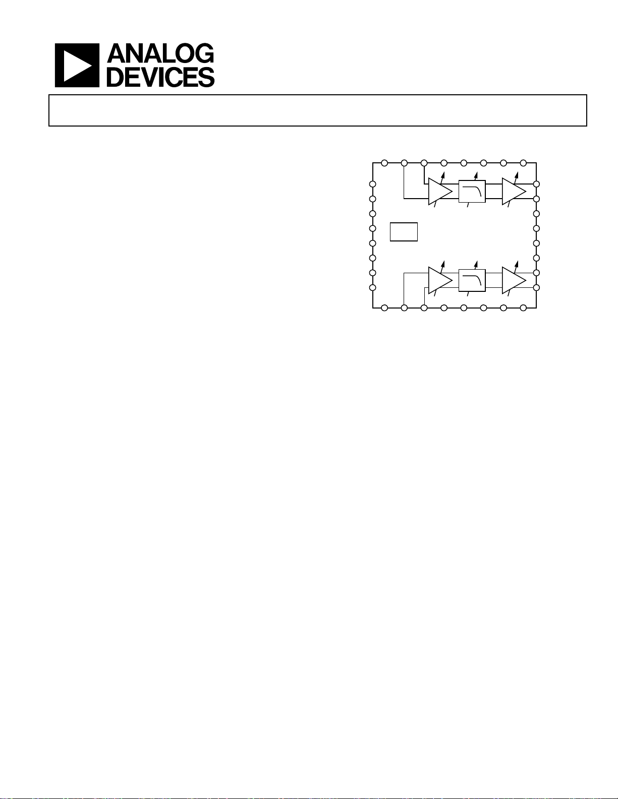
FUNCTIONAL BLOCK DIAGRAM
INP1 INM1
ENBL
VPSD
COMD
LE
CLK
DATA
SDO
COM
VPS
SPI
COM I NP2 INM2 VPS COM OFDS OFS2 V PS
PS
COM GNSW OFS1VPS
ADRF6510
Figure 1.
OPP1
OPM1
COM
GAIN
VOCM
COM
OPM2
OPP2
09002-001
GENERAL DESCRIPTION
The ADRF6510 is a matched pair of fully differential low noise
and low distortion programmable filters and variable gain amplifiers (VGAs). Each channel is capable of rejecting large out-ofband interferers while reliably boosting the wanted signal, thus
reducing the bandwidth and resolution requirements on the
analog-to-digital converters (ADCs). The excellent matching
between channels and their high spurious-free dynamic range
over all gain and bandwidth settings makes the ADRF6510
ideal for quadrature-based (IQ) communication systems with
dense constellations, multiple carriers, and nearby interferers.
The filters provide a six-pole Butterworth response with 0.5 dB
corner frequencies programmable through the SPI port from
1 MHz to 30 MHz in 1 MHz steps. The preamplifier that precedes
the filters offers a pin-programmable option of either 6 dB or
12 dB of gain. The preamplifier sets a differential input impedance of 400 and has a common-mode voltage that defaults
to 2.1 V but can be driven from 1.5 V to 2.5 V.
The variable gain amplifiers that follow the filters provide 50 dB
of continuous gain control with a slope of 30 mV/dB. The output
buffers provide a differential output impedance of 20 Ω that is
capable of driving 1.5 V p-p into 1 kΩ loads. The output commonmode voltage defaults to VPS/2, but it can be programmed via the
VOCM pin. The built-in dc offset correction loop can be disabled
if dc-coupled operation is desired. The high-pass corner frequency
is defined by external capacitors on the OFS1 and OFS2 pins.
The ADRF6510 operates from a 4.75 V to 5.25 V supply and
consumes a maximum supply current of 258 mA when programmed to the highest bandwidth setting. When disabled, it
consumes 2 mA. The ADRF6510 is fabricated in an advanced
silicon-germanium BiCMOS process and is available in a
32-lead, exposed paddle LFCSP. Performance is specified over
the −40°C to +85°C temperature range.
Rev. A
Information furnished by Analog Devices is believed to be accurate and reliable. However, no
responsibility is assumed by Anal og Devices for its use, nor for any infringements of patents or ot her
rights of third parties that may result from its use. Specifications subject to change without notice. No
license is granted by implication or otherwise under any patent or patent rights of Analog Devices.
Trademarks and registered trademarks are the property of their respective owners.
One Technology Way, P.O. Box 9106, Norwood, MA 02062-9106, U.S.A.
Tel: 781.329.4700 www.analog.com
Fax: 781.461.3113 ©2010-2011 Analog Devices, Inc. All rights reserved.
Page 2

ADRF6510 Data Sheet
TABLE OF CONTENTS
Features.............................................................................................. 1
Applications....................................................................................... 1
Functional Block Diagram ..............................................................1
General Description......................................................................... 1
Revision History ...............................................................................2
Specifications..................................................................................... 3
Timing Diagrams.......................................................................... 5
Absolute Maximum Ratings............................................................ 6
ESD Caution.................................................................................. 6
Pin Configuration and Function Descriptions............................. 7
Typical Performance Characteristics............................................. 8
Theory of Operation ......................................................................15
Input Buffers ...............................................................................15
Programmable Filters.................................................................15
Variable Gain Amplifiers (VGAs)............................................ 16
Output Buffers/ADC Drivers ................................................... 16
DC Offset Compensation Loop................................................ 16
Programming the Filters............................................................17
Noise Characteristics .................................................................17
Distortion Characteristics......................................................... 18
Maximizing the Dynamic Range.............................................. 18
Key Parameters for Quadrature-Based Receivers.................. 19
Applications Information.............................................................. 20
Basic Connections...................................................................... 20
Error Vector Magnitude (EVM) Performance........................... 20
EVM............................................................................................. 21
Effect of Filter Bandwidth on EVM......................................... 21
Effect of Output Voltage Levels on EVM ................................ 21
Effect of C
Anti-Aliasing Filter.................................................................... 22
Evaluation Board............................................................................ 24
Evaluation Board Control Software......................................... 24
Schematics and Artwork ...........................................................24
Evaluation Board Configuration Options............................... 27
Outline Dimensions....................................................................... 29
Ordering Guide .......................................................................... 29
on EVM ............................................................... 22
OFS
REVISION HISTORY
10/11—Rev. 0 to Rev. A
Changes to Figure 2 and Figure 3................................................... 5
Changes to Table 3............................................................................ 7
Changes to Figure 48, Changes to Error Vector Magnitude
(EVM) Performance Section......................................................... 20
Deleted Low IF Image Rejection Section, and Example
Baseband Interface Section, Figure 50, and Figure 51;
Renumbered Subsequent Figures................................................. 20
Changes to Figure 49...................................................................... 21
Added EVM Section, Effect of Filter Bandwidth on EVM
Section, Effect of Output Voltage Levels on EVM Section, and
Effect of C
Added Anti-Aliasing Filter Section.............................................. 22
Changes to Figure 54...................................................................... 22
Changes to Figure 58...................................................................... 24
Changes to Figure 61...................................................................... 25
Changes to Figure 62 and Figure 63............................................. 26
Changes to Table 5.......................................................................... 27
4/10—Revision 0: Initial Version
on EVM Section...................................................... 21
OFS
Rev. A | Page 2 of 32
Page 3

Data Sheet ADRF6510
SPECIFICATIONS
VPS = 5 V, TA = 25°C, Z
Table 1.
Parameter Test Conditions/Comments Min Typ Max Unit
FREQUENCY RESPONSE
Low-Pass Corner Frequency, fC Six-pole Butterworth filter, 0.5 dB bandwidth 1 30 MHz
Step Size 1 MHz
Corner Frequency Absolute
Accuracy
Corner Frequency Matching
Pass-Band Ripple 0.5 dB p-p
Gain Matching
Group Delay Variation From midband to peak
Corner Frequency = 1 MHz 135 ns
Corner Frequency = 30 MHz 11 ns
Group Delay Matching Channel A and Channel B at same gain
Corner Frequency = 1 MHz 5 ns
Corner Frequency = 30 MHz 0.2 ns
Stop-Band Rejection
Relative to Pass Band 2 × fC 30 dB
5 × fC 75 dB
INPUT STAGE INP1, INM1, INP2, INM2
Maximum Input Swing At minimum gain, V
Differential Input Impedance 400 Ω
Input Common-Mode Range 1 V p-p input voltage 1.5 VPS/2 V
Input pins left floating VPS/2 V
GAIN CONTROL GAIN, GNSW
Voltage Gain Range GNSW = 0 V, V
GNSW = 5 V 1 51 dB
Gain Slope 30 mV/dB
Gain Error V
Gain Step GNSW = 0 V to 5 V 6 dB
OUTPUT STAGE OPP1, OPM1, OPP2, OPM2, VOCM
Maximum Output Swing At maximum gain, R
HD2 > 60 dBc, HD3 > 60 dBc 1.5 V p-p
Differential Output Impedance 20 Ω
Output DC Offset Inputs shorted, offset loop disabled 35 mV
Output Common-Mode Range 1.5 V p-p output voltage 1.5 3.0 V
VOCM left floating VPS/2 V
NOISE/DISTORTION
1 MHz Corner Frequency
Output Noise Density Gain = 0 dB at fC/2 −129 dBV/√Hz
Gain = 20 dB at fC/2 −127 dBV/√Hz
Gain = 40 dB at fC/2 −111 dBV/√Hz
Second Harmonic, HD2 250 kHz fundamental, 1.5 V p-p output voltage
Gain = 0 dB 46.2 dBc
Gain = 40 dB 43.2 dBc
Third Harmonic, HD3 250 kHz fundamental, 1.5 V p-p output voltage
Gain = 0 dB 52.2 dBc
Gain = 40 dB 51.2 dBc
SOURCE
= 400 Ω, Z
= 1 kΩ, V
LOAD
= 1.5 V p-p, bandwidth setting = 30 MHz, GNSW = 0 V, unless otherwise noted.
OUT
Over operating temperature range ±15 % f
Channel A and Channel B at same gain and
±0.5 % f
bandwidth settings
Channel A and Channel B at same gain and
±0.1 dB
bandwidth settings
= 0 V 1 V p-p
GAIN
from 0 V to 2 V −5 +45 dB
GAIN
from 500 mV to 1.7 V 0.2 dB
GAIN
= 1 kΩ 2 V p-p
LOAD
C
C
Rev. A | Page 3 of 32
Page 4

ADRF6510 Data Sheet
Parameter Test Conditions/Comments Min Typ Max Unit
IMD3
f1 = 500 kHz, f2 = 550 kHz, 1.5 V p-p composite
output voltage
Gain = 5 dB 61 dBc
Gain = 35 dB 57 dBc
IMD3 with Input CW Blocker
f1 = 500 kHz, f2 = 550 kHz, 1.5 V p-p composite
output, gain = 5 dB; blocker at 5 MHz, 10 dBc
relative to two-tone composite output voltage
30 MHz Corner Frequency
Output Noise Density Midband, gain = 0 dB −130 dBV/√Hz
Midband, gain = 20 dB −130 dBV/√Hz
Midband, gain = 40 dB −123 dBV/√Hz
Second Harmonic, HD2 8 MHz fundamental, 1.5 V p-p output voltage
Gain = 0 dB 63 dBc
Gain = 40 dB 84 dBc
Third Harmonic, HD3 8 MHz fundamental, 1.5 V p-p output voltage
Gain = 0 dB 54 dBc
Gain = 40 dB 87 dBc
IMD3
f1 = 15 MHz, f2 = 16 MHz, 1.5 V p-p composite
output voltage
Gain = 5 dB 59 dBc
Gain = 35 dB 77.5 dBc
IMD3 with Input CW Blocker
f1 = 15 MHz, f2 = 16 MHz, 1.5 V p-p composite
output, gain = 5 dB; blocker at 150 MHz, 10 dBc
relative to two-tone composite output voltage
DIGITAL LOGIC LE, CLK, DATA, SDO, OFDS, GNSW
Input High Voltage, V
Input Low Voltage, V
Input Current, I
INH/IINL
>2 V
INH
<0.8 V
INL
<1 μA
Input Capacitance, CIN 2 pF
SPI TIMING LE, CLK, DATA, SDO
f
1/t
CLK
20 MHz
CLK
tDH DATA hold time 5 ns
tDS DATA setup time 5 ns
tLH LE hold time 5 ns
tLS LE setup time 5 ns
tPW CLK high pulse width 5 ns
tD CLK to SDO delay 5 ns
POWER AND ENABLE VPS, VPSD, COM, COMD, ENBL
Supply Voltage Range 4.75 5.0 5.25 V
Total Supply Current ENBL = 5 V
Maximum bandwidth setting 258 mA
Minimum bandwidth setting 131 mA
Disable Current ENBL = 0 V 2 mA
Disable Threshold 2.5 V
Enable Response Time Delay following ENBL low-to-high transition 20 μs
Disable Response Time Delay following ENBL high-to-low transition 300 ns
40 dBc
55 dBc
Rev. A | Page 4 of 32
Page 5
Data Sheet ADRF6510
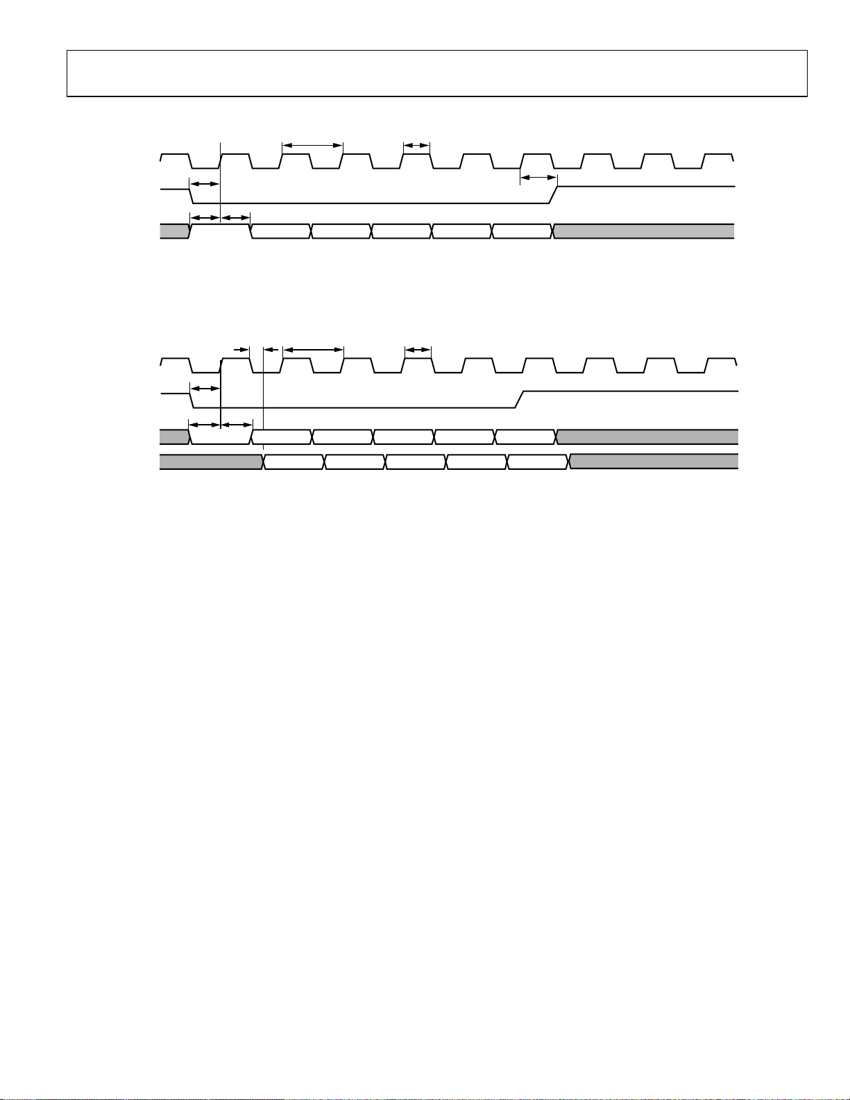
TIMING DIAGRAMS
t
CLK
CLK
LE
DATA
NOTES
1. THE FIRST DATA BIT DETERMINES WHETHER THE PART IS WRITING TO OR READING F ROM THE I NTERNAL CORNER FREQUENC Y
WORD REGISTER. FOR A WRITE O PERATION, THE FIRST BIT SHO ULD BE A LOGIC 1. THE CORNER FREQUENCY WORD BIT I S THEN
REGISTERE D INTO THE DATA PIN ON CONSECUTIVE RISING EDGES O F THE CLO CK.
t
LS
tDSt
DH
WRITE BIT
LSB + 1LSB
Figure 2. Write Mode Timing Diagram
t
CLK
DCDCREAD BIT DC DC DC
CLK
LE
DATA
t
t
LS
tDSt
D
DH
t
PW
MSB – 2 MSB – 1 MSB
t
PW
MSB - 2
t
LH
09002-003
SDO
NOTES
1. THE FIRST DAT A BIT DET ERMINES WHETHER T HE PART I S WRIT ING TO OR READING FROM T HE INTE RNAL CORNER FREQUENCY WORD
REGIST ER. FO R A READ OPERAT ION, THE FI RST BIT SHOULD BE A LOGI C 0. THE CO RNER FREQ UENCY WORD BIT IS THEN UPDATED AT
THE SDO PIN ON CONSECUTIVE FALLING EDGES OF THE CLOCK.
LSB + 1LSB
MSB – 2
MSB – 1 MSB
09002-004
Figure 3. Read Mode Timing Diagram
Rev. A | Page 5 of 32
Page 6
ADRF6510 Data Sheet
ABSOLUTE MAXIMUM RATINGS
Table 2.
Parameter Rating
Supply Voltages, VPS, VPSD 5.25 V
ENBL, GNSW, OFDS, LE, CLK, DATA, SDO VPS + 0.6 V
INP1, INM1, INP2, INM2
OPP1, OPM1, OPP2, OPM2 VPS + 0.6 V
OFS1, OFS2 VPS + 0.6 V
GAIN VPS + 0.6 V
Internal Power Dissipation 1.4 W
θJA (Exposed Pad Soldered to Board) 37.4°C/W
Maximum Junction Temperature 150°C
Operating Temperature Range −40°C to +85°C
Storage Temperature Range −65°C to +150°C
Lead Temperature (Soldering 60 sec) 300°C
VPS + 0.6 V,
GND − 0.6 V
Stresses above those listed under Absolute Maximum Ratings
may cause permanent damage to the device. This is a stress
rating only; functional operation of the device at these or any
other conditions above those indicated in the operational
section of this specification is not implied. Exposure to absolute
maximum rating conditions for extended periods may affect
device reliability.
ESD CAUTION
Rev. A | Page 6 of 32
Page 7
Data Sheet ADRF6510
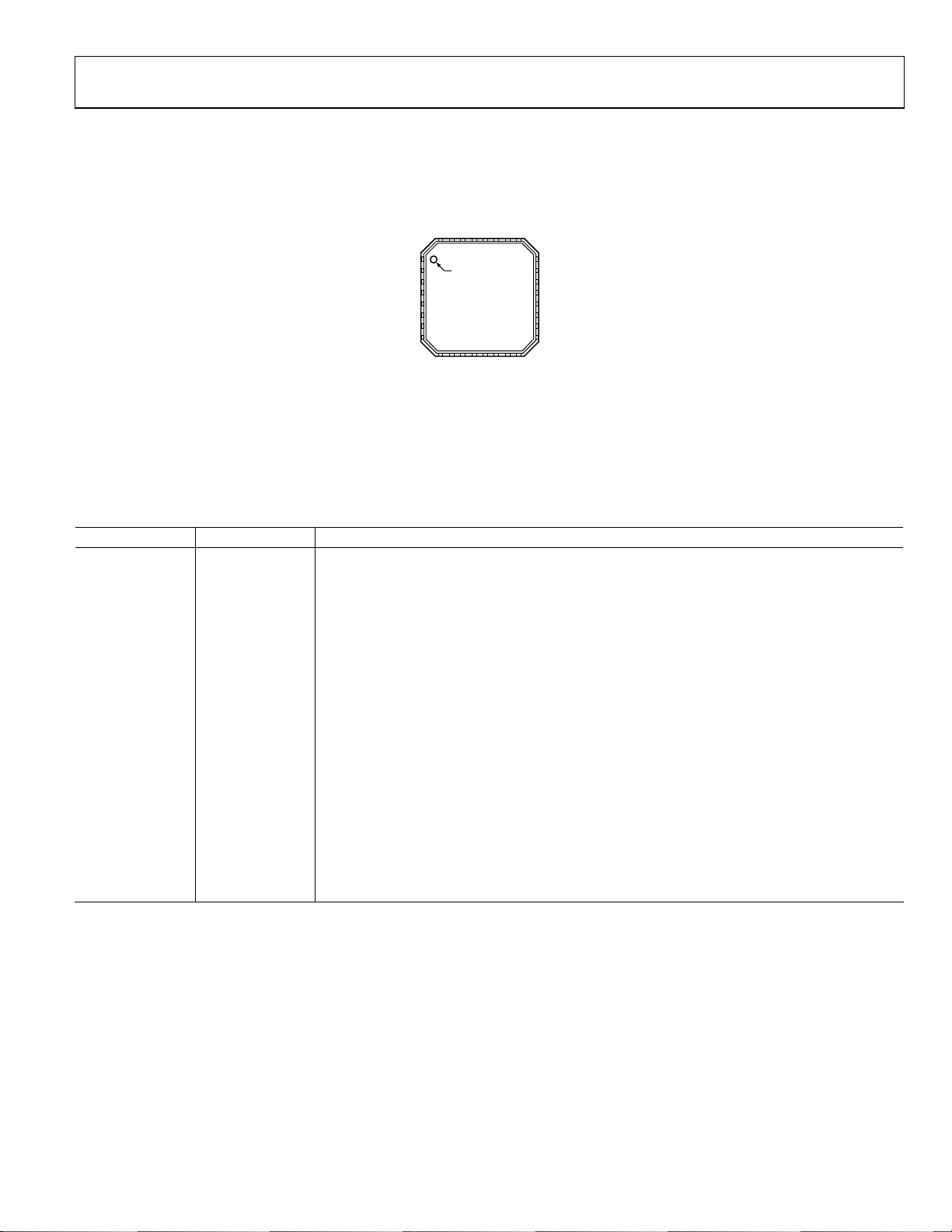
W
PIN CONFIGURATION AND FUNCTION DESCRIPTIONS
L
M1
COM
GNS
OFS1
ENB
INP1
IN
31
30
32
VPS
VPS
26
25
28
27
29
1VPSD
PIN 1
2COMD
INDICATOR
3LE
4CLK
ADRF6510
5DATA
TOP VIEW
6SDO
(Not to Scal e)
7COM
8VPS
1
9
1
10
12
13
VPS
INP2
COM
COM
INM2
NOTES
1. CONNECT THE EXPOSED PADDLE TO
A LOW IMPEDANCE GROUND PAD.
24 OPP1
23 O PM1
22 CO M
21 G AIN
20 V OCM
19 CO M
18 O PM2
17 O PP2
14
15
16
VPS
OFS2
OFDS
09002-002
Figure 4. Pin Configuration
Table 3. Pin Function Descriptions
Pin No. Mnemonic Description
1 VPSD Digital Positive Supply Voltage: 4.75 V to 5.25 V.
2 COMD Digital Common. Connect to external circuit common using the lowest possible impedance.
3 LE Latch Enable. SPI programming pin. CMOS levels: V
4 CLK SPI Port Clock. CMOS levels: V
5 DATA SPI Data Input. CMOS levels: V
6 SDO SPI Data Output. CMOS levels: V
< 0.8 V, V
LOW
< 0.8 V, V
LOW
LOW
< 0.8 V, V
HIGH
HIGH
> 2 V.
> 2 V.
HIGH
LOW
> 2 V.
< 0.8 V, V
HIGH
> 2 V.
7, 9, 13, 19, 22, 28 COM Analog Common. Connect to external circuit common.
8, 12, 16, 25, 29 VPS Analog Positive Supply Voltage: 4.75 V to 5.25 V.
10, 11, 30, 31
INP2, INM2,
Differential Inputs. 400 Ω input impedance. Common-mode range is 1.5 V to 2.5 V; default is 2.1 V.
INM1, INP1
14 OFDS Offset Correction Loop Disable. Pull high to disable the offset correction loop.
15, 26 OFS2, OFS1 Offset Correction Loop Compensation Capacitors. Connect capacitors to circuit common.
17, 18, 23, 24
OPP2, OPM2,
Differential Outputs. 20 Ω output impedance. Common-mode range is 1.5 V to 3 V; default is VPS/2.
OPM1, OPP1
20 VOCM Output Common-Mode Setpoint. Defaults to VPS/2 if left open.
21 GAIN Analog Gain Control. 0 V to 2 V, 30 mV/dB gain scaling.
27 GNSW Front-End Gain Switch, 6 dB or 12 dB. Pull low for 6 dB; pull high for 12 dB.
32 ENBL Chip Enable. Pull high to enable.
EP Exposed Paddle. Connect the exposed paddle to a low impedance ground pad.
Rev. A | Page 7 of 32
Page 8
ADRF6510 Data Sheet
TYPICAL PERFORMANCE CHARACTERISTICS
VPS = 5 V, TA = 25°C, Z
50
BANDWIDTH = 30MHz
45
40
35
30
25
20
–40°C
VPS = 4.75V, 5V, 5.25V
15
GAIN (dB)
10
5
0
–5
–10
0 200 400 600 800 1000 1200 1400 1600 1800 22002000
Figure 5. In-Band Gain vs. V
(Bandwidth Setting = 30 MHz)
= 400 Ω, Z
SOURCE
+25°C
VPS = 4.75V, 5V, 5.25V
+85°C
VPS = 4.75V, 5V, 5.25V
V
(mV)
GAIN
over Supply and Temperature
GAIN
= 1 kΩ, V
LOAD
= 1.5 V p-p, GNSW = 0 V, unless otherwise noted.
OUT
3.0
BANDWIDTH = 30MHz
2.5
2.0
1.5
1.0
0.5
0
–0.5
–1.0
GAIN ERROR (dB)
–1.5
–2.0
–2.5
–3.0
0 200 400 600 800 1000 1200 1400 1600 1800 2000 2200 2400
09002-005
+85°C
VPS = 4.25V, 5V, 5.25V
+25°C
VPS = 4.25V, 5V, 5.25V
Figure 8. Gain Conformance vs. V
(Bandwidth Setting = 30 MHz)
–40°C
VPS = 4.25V, 5V, 5.25V
V
(mV)
GAIN
over Supply and Temperature
GAIN
09002-008
50
45
40
35
30
25
20
15
10
5
0
–5
GAIN (dB)
–10
–15
–20
–25
–30
–35
–40
–45
–50
1 10 100
Figure 6. Gain vs. Frequency by V
0.25
0.20
0.15
0.10
FREQUENCY (MHz)
GAIN
BANDWIDTH = 30MHz
(Bandwidth Setting = 30 MHz)
BANDWIDTH = 30MHz
5
3
1
–1
–3
GAIN ERROR (dB)
–5
–7
–9
09002-006
PREAMP GAIN = 12dB
PREAMP GAIN = 6dB
0 5 10 15 4035302520
FREQUENCY (MHz )
BANDWIDTH = 30MHz
9
8
7
6
5
GAIN STEP (dB)
4
3
2
09002-009
Figure 9. 6 dB Gain Step and Gain Error vs. Frequency
(Bandwidth Setting = 30 MHz, V
15
10
5
0
= 0 V)
GAIN
PREAMP GAIN = 6dB
PREAMP GAIN = 12dB
0.05
GAIN MISMATCH (dB)
0
–0.05
02
0.20.40.60.81.01.21.41.61.82.0 .2
Figure 7. Gain Matching vs. V
V
(V)
GAIN
(Bandwidth Setting = 30 MHz)
GAIN
09002-007
OP1dB (dBV rms)
–5
–10
–15
0 5 10 15 20 25 30 35 40
Figure 10. Output P1dB vs. GAIN at 15 MHz (Bandwidth Setting = 30 MHz)
Rev. A | Page 8 of 32
GAIN (dB)
09002-010
Page 9
Data Sheet ADRF6510
40
35
30
25
20
15
GAIN (dB)
10
5
0
–5
–10
1M 100M10M
FREQUENCY (Hz)
Figure 11. Frequency Response vs. Bandwidth Setting (Gain = 30 dB),
Log Scale
09002-011
1000
GAIN = 20dB
900
800
700
600
500
400
GROUP DELAY (ns)
300
200
100
0
0.5 5 50
BW = 1MHz
BW = 5MHz
BW = 10MHz
BW = 20MHz
FREQUENCY (MHz )
Figure 14. Group Delay vs. Frequency (Gain = 20 dB)
BW = 30MHz
09002-014
32
31
30
GAIN (dB)
29
28
27
140
6 111621263136
FREQUENCY (MHz)
09002-012
Figure 12. Frequency Response vs. Bandwidth Setting (Gain = 30 dB),
1.0
BANDWIDTH = 30MHz
0.5
0
–0.5
GROUP DELAY MATCHING (ns)
–1.0
0.5 5 30
Figure 15. Group Delay Mismatch vs. Frequency
Linear Scale
30
29
28
27
26
25
24
23
22
GAIN (dB)
21
20
19
18
17
16
15
4 6 8 101214161820222426283032343638
240
–40°C
+85°C
FREQUENCY (MHz )
+25°C
09002-013
Figure 13. Frequency Response over Temperature
5
BANDWIDTH = 1MHz
4
3
2
1
0
–1
–2
–3
IQ GROUP DE LAY MATCHING (ns)
–4
–5
0.2 0. 4 0.6 0.8 1.0 1. 2 1. 4
Figure 16. IQ Group Delay Mismatch vs. Frequency
(Gain = 26 dB, Bandwidth Setting = 30 MHz)
GAIN = 20dB
GAIN = 40dB
FREQUENCY (MHz )
(Bandwidth Setting = 30 MHz)
GAIN = 20dB
GAIN = 0dB
FREQUENCY (MHz )
(Bandwidth Setting = 1 MHz)
09002-015
09002-016
Rev. A | Page 9 of 32
Page 10
ADRF6510 Data Sheet
0 0.51.01.52.02.53.0
0.75
0.50
0.25
BANDWIDTH = 30MHz
0
–0.25
IQ AMPLITUDE MISMAT CH (dB)
–0.50
–0.75
03
5 10152025
FREQUENCY (MHz )
FREQUENCY (MHz )
BANDWIDTH = 1MHz
0
09002-017
Figure 17. IQ Amplitude Mismatch vs. Frequency
100
90
80
70
60
HD3 @ 24MHz (dBc)
50
40
04
5 101520253035
GAIN (dB)
+25°C, VPS = 4.75V
+25°C, VPS = 5V
+25°C, VPS = 5.25V
+85°C, VPS = 4.75V
+85°C, VPS = 5V
+85°C, VPS = 5.25V
–40°C, VPS = 4.75V
–40°C, VPS = 5V
–40°C, VPS = 5.25V
0
09002-020
Figure 20. HD3 vs. Gain over Supply and Temperature
(Bandwidth Setting = 30 MHz)
90
85
80
75
70
65
60
HD2 @ 16MHz (dBc)
55
50
45
40
040
5 101520253035
GAIN (dB)
+25°C, VPS = 4.75V
+25°C, VPS = 5V
+25°C, VPS = 5.25V
+85°C, VPS = 4.75V
+85°C, VPS = 5V
+85°C, VPS = 5.25V
–40°C, VPS = 4.75V
–40°C, VPS = 5V
–40°C, VPS = 5.25V
09002-018
Figure 18. HD2 vs. Gain over Supply and Temperature
100
1.5V p-p OUTPUT @ 8MHz
BANDWIDTH = 30MHz
90
80
70
60
HD3 @ 24MHz (dBc)
50
40
04
5 101520253035
Figure 21. HD3 vs. Gain over Output Common-Mode Voltage
(Bandwidth Setting = 30 MHz)
100
1.5V p-p OUTPUT @ 8MHz
BANDWIDTH = 30MHz
90
80
70
60
HD2 @ 16MHz (dBc)
50
40
30
0 5 10 15 20 25 30 35 40
GAIN (dB)
VOCM = 1.5V
VOCM = 1.75V
VOCM = 2V
VOCM = 2.5V
Figure 19. HD2 vs. Gain over Output Common-Mode Voltage
09002-019
30
BANDWIDTH = 30MHz
f1 = 14MHz, f2 = 15MHz
25
PREAMP
GAIN = 6dB
20
15
OIP3 (dBV)
10
5
0
05 504540353025201510
Figure 22. In-Band OIP3 vs. Gain (Bandwidth Setting = 30 MHz)
(Bandwidth Setting = 30 MHz)
GAIN (dB)
(Bandwidth Setting = 30 MHz)
PREAMP
GAIN = 12dB
GAIN (dB)
VOCM = 1.5V
VOCM = 1.75V
VOCM = 2V
VOCM = 2.5V
0
09002-021
09002-022
Rev. A | Page 10 of 32
Page 11

Data Sheet ADRF6510
30
BANDWIDTH = 30MHz
f1 = 14MHz, f2 = 15MHz
25
+25°C
20
15
OIP3 (dBV)
10
5
0
043530252015105
+85°C
GAIN (dB)
Figure 23. In-Band OIP3 vs. Gain over Temperature
(Preamp Gain = 6 dB, Bandwidth Setting = 30 MHz)
–40°C
0
09002-023
65
55
BANDWIDTH = 30MHz
45
35
25
15
5
–5
–15
–25
–35
–45
PREAMP
–55
GAIN = 12dB
–65
–75
IMD2 @ 15MHz (dBV)
–85
–95
–105
–115
–125
–135
–145
–45 65
–35 –25 –15 –5 5 15 25 35
INPUT LEV EL @ 115MHz AND 130MHz (dBV/To ne)
2:1 SLOPE
PREAMP
GAIN = 6dB
OUT-OF -BAND IIP2
Figure 26. Out-of-Band IIP2: IMD2 Tone at Midband
(Bandwidth Setting = 30 MHz)
55
5
4
09002-060
120
100
80
60
IMD3 (d Bc)
40
20
0
0 0.5 1.0 1.5 2.0 2.5 3.0 3.5 4.0
COMPOSIT E OUTPUT VOLTAG E (V p-p)
GAIN = 0dB
GAIN = 10dB
GAIN = 20dB
GAIN = 30dB
GAIN = 40dB
Figure 24. In-Band Third-Order Intermodulation Distortion
(Preamp Gain = 6 dB, Bandwidth Setting = 30 MHz)
120
100
80
60
IMD3 (d Bc)
40
20
0
0 0.5 1.0 1.5 2.0 2.5 3.0 3.5 4.0
COMPOSIT E OUTPUT VOLTAG E (V p-p)
GAIN = 6dB
GAIN = 16dB
GAIN = 26dB
GAIN = 36dB
GAIN = 46dB
Figure 25. In-Band Third-Order Intermodulation Distortion
(Preamp Gain = 12 dB, Bandwidth Setting = 30 MHz)
10
BANDWIDTH = 30MHz
0
–10
–20
–30
–40
–50
–60
PREAMP
–70
GAIN = 12dB
–80
IMD3 @ 15MHz (dBV)
–90
–100
–110
–120
–130
–45 5
–40 –35 –30 –25 –20 –15 –10 –5 0
09002-024
INPUT LEVEL @ 115MHz AND 215M Hz (dBV/T one)
3:1 SLOPE
PREAMP
GAIN = 6dB
OUT-OF -BAND IIP3
09002-027
Figure 27. Out-of-Band IIP3: IMD3 Tone at Midband
(Bandwidth Setting = 30 MHz)
70
65
60
55
50
45
40
35
NOISE FI GURE (dB re 50)
30
25
20
–5 0 5 10 15 20 25 30 35 40 45
09002-025
GAIN (dB)
1MHz BW
2MHz BW
4MHz BW
6MHz BW
8MHz BW
30MHz BW
09002-028
Figure 28. Noise Figure vs. Gain over Bandwidth Setting,
Preamp Gain = 6 dB (Noise Figure at 1/2 Bandwidth)
Rev. A | Page 11 of 32
Page 12

ADRF6510 Data Sheet
–
–
–
–
–
60
55
50
45
40
35
30
25
NOISE FI GURE (dB re 50)
20
15
10
0 5 10 15 20 25 30 35 40 45 50
GAIN (dB)
Figure 29. Noise Figure vs. Gain over Bandwidth Setting,
Preamp Gain = 12 dB (Noise Figure at 1/2 Bandwidth)
1MHz BW
2MHz BW
4MHz BW
6MHz BW
8MHz BW
30MHz BW
09002-029
90
–95
–100
Hz)
–105
–110
–115
–120
–125
OUTPUT NOISE (dBV rms/
–130
–135
–140
0.5 3.02.52.01.51.0
FREQUENCY (MHz)
GAIN = 0dB
GAIN = 20dB
GAIN = 40dB
09002-032
Figure 32. Output Noise Density vs. Frequency (Bandwidth Setting = 1 MHz)
100
–105
–110
–115
–120
–125
OUTPUT NOISE (dBV rms/Hz)
–130
–135
1MHz BW
2MHz BW
4MHz BW
6MHz BW
8MHz BW
30MHz BW
–5 0 5 10 15 20 25 30 35 40 45
GAIN (dB)
Figure 30. Output Noise Density vs. Gain by Bandwidth Setting,
Preamp Gain = 6 dB (Noise at 1/2 Bandwidth)
100
–105
–110
–115
–120
–125
OUTPUT NOISE (dBV rms/Hz)
–130
–135
1MHz BW
2MHz BW
4MHz BW
6MHz BW
8MHz BW
30MHz BW
0 5 10 15 2 0 25 30 35 40 45 50
GAIN (dB)
Figure 31. Output Noise Density vs. Gain by Bandwidth Setting,
Preamp Gain = 12 dB (Noise at 1/2 Bandwidth)
110
GAIN = 0dB
–115
Hz)
–120
–125
–130
OUTPUT NOISE (dBV rms/
–135
–140
09002-030
10 3018 20 22 24 26 28161412
FREQUENCY (MHz)
GAIN = 20dB
GAIN = 40dB
09002-033
Figure 33. Output Noise Density vs. Frequency (Bandwidth Setting = 20 MHz)
90
–95
–100
–105
–110
–115
–120
–125
–130
OUTPUT NOISE @ 15MHz (dBV/Hz)
–135
–140
09002-031
–35 –30 –25 –20 –15 –10
BLOCKER LEVEL @ 150MHz (d BV rms)
GAIN = 40dB
GAIN = 20dB
GAIN = 0dB
09002-034
Figure 34. Output Noise Density vs. Blocker Level
(Bandwidth Setting = 30 MHz, Blocker at 150 MHz)
Rev. A | Page 12 of 32
Page 13

Data Sheet ADRF6510
450
440
430
420
410
()
400
IN
R
390
380
370
360
350
0 5 10 15 20 25 30
FREQUENCY (MHz )
10
5
0
–5
–10
–15
–20
–25
–30
–35
–40
Figure 35. Input Impedance vs. Frequency (Bandwidth Setting = 30 MHz)
(pF)
IN
C
09002-035
280
260
240
220
200
(mA)
180
SUPPLY
I
160
140
120
100
0 5 10 15 20 25 30
BANDWIDTH SETT ING (MHz)
Figure 38. Current Consumption vs. Bandwidth Setting (Gain = 20 dB)
09002-038
28
27
26
25
()
24
SERIES_OUT
23
R
22
21
20
03
510152025
FREQUENCY (MHz )
Figure 36. Output Impedance vs. Frequency (Bandwidth Setting = 30 MHz)
90
BANDWIDTH = 30MHz
80
70
60
50
40
ISOLATION (dB)
30
20
10
0
0.1 1 10 100
GAIN = 40dB
GAIN = 20dB
GAIN = 0dB
FREQUENCY (MHz )
Figure 37. Channel Isolation, Output to Output, vs. Frequency
200
100
0
–100
(nH)
–200
–300
SERIES_OUT
L
–400
–500
–600
0
09002-036
266
264
262
260
258
(mA)
256
SUPPLY
I
254
252
250
248
–50 –30 –10 10 30 50 70 90
Figure 39. Current Consumption vs. Temperature over Supply
70
BANDWIDTH = 30MHz
60
50
40
30
CMRR (dB)
20
10
0
03
09002-037
Figure 40. Common-Mode Rejection Ratio vs. Frequency
(Bandwidth Setting = 30 MHz)
VPS = 4.75V
VPS = 5V
VPS = 5.25V
TEMPERATURE ( °C)
09002-039
(Bandwidth Setting = 30 MHz)
GAIN = 40dB
GAIN = 20dB
5 10152025 0
FREQUENCY (MHz)
09002-040
(Bandwidth Setting = 30 MHz)
Rev. A | Page 13 of 32
Page 14

ADRF6510 Data Sheet
30MHz BANDWIDTH,
28MHz MAINTONE
28MHz SIGNA L = 45mV p-p
TO 450mV p- p
INPUT SIGNAL = 45mV p-p
OUTPUT SI GNAL = 450mV p-p
20dB OF GAIN
V
GAIN
400ns/DIV
V
= 1400mV
GAIN
TO 800mV
= 800mV TO 1. 40V
09002-067
Figure 41. Gain Step Response
Rev. A | Page 14 of 32
Page 15

Data Sheet ADRF6510
THEORY OF OPERATION
The ADRF6510 consists of a matched pair of buffered, programmable filters followed by variable gain amplifiers and output
ADC drivers. The block diagram of a single channel is shown
in Figure 42. The programmability of the bandwidth and of the
pre- and post-filtering gain offers great flexibility when coping
with signals of varying levels in the presence of noise and large,
undesired signals nearby. The entire differential signal chain is
dc-coupled with flexible interfaces at the input and output. The
bandwidth and gain setting controls for the two channels are
shared, ensuring close matching of their magnitude and phase
responses. The ADRF6510 can be fully disabled through the
ENBL pin.
6dB/12dB
PREAMP
BASEBAND
INPUTS
PREAMP
GAIN SWITCH
Figure 42. Signal Path Block Diagram for a Single Channel of the ADRF6510
1MHz TO 30MHz
PROG. FILTERS
SPI
INTERFACE
FILTER
PROGRAMMI NG
SPI BUS
50dB
VGA
ANALOG
GAIN CONT ROL
30mV/dB
OUTPUT ADC
DRIVER
COMMON-MODE
BASEBAND
OUTPUTS
OUTPUT
CONTROL
Filtering and amplification are fundamental operations in any
signal processing system. Filtering is necessary to select the
intended signal while rejecting out-of-band noise and interferers.
Amplification increases the level of the desired signal to overcome
noise added by the system. When used together, filtering and
amplification can extract a low level signal of interest in the
presence of noise and out-of-band interferers. Such analog
signal processing alleviates the requirements on the analog,
mixed signal, and digital components that follow.
INPUT BUFFERS
The input buffers provide a convenient interface to the sensitive
filter sections that follow. They set a differential input impedance
of 400 Ω and sit at a nominal common-mode voltage of VPS/2.
The inputs can be dc-coupled or ac-coupled. If using direct
dc-coupling, the common-mode voltage, V
, can range from
CM
1.5 V to 3 V. A current flows into or out of the input pins to
accommodate the difference in common-mode voltages. The
current into each pin is given by
(V
– (VPS/2))/200 Ω
CM
The input buffers in both channels can be configured simultaneously to a gain of 6 dB or 12 dB through the GNSW pin. When
configured for a 6 dB gain, the buffers support up to a 1 V p-p
differential input level with >50 dBc harmonic distortion. For
a 12 dB gain setting, the buffers support 0.5 V p-p inputs.
PROGRAMMABLE FILTERS
The integrated programmable filter is the key signal processing
function in the ADRF6510. The filters follow a six-pole Butterworth prototype response that provides a compromise between
band rejection, ripple, and group delay. The 0.5 dB bandwidth is
programmed from 1 MHz to 30 MHz in 1 MHz steps via the serial
programming interface (SPI) as described in the Programming
the Filters section.
The filters are designed so that the Butterworth prototype filter
shape and group delay responses vs. frequency are retained for
any bandwidth setting. Figure 43 and Figure 44 illustrate the
ideal six-pole Butterworth gain and group delay responses,
respectively. The group delay, τ
τ
= −∂φ/∂ω
g
, is defined as
g
where:
φ is the phase in radians.
ω = 2πf is the frequency in radians/second.
Note that for a frequency scaled filter prototype, the absolute
magnitude of the group delay scales inversely with the bandwidth; however, the shape is retained. For example, the peak
group delay for a 28 MHz bandwidth setting is 14× less than
for a 2 MHz setting.
0
09002-042
–20
–40
–60
–80
–100
–120
RELATIVE MAGNITUDE (Hz)
–140
–160
–180
1M 10M 100M 1G
FREQUENCY (Hz)
Figure 43. Sixth-Order Butterworth Magnitude Response for 0.5 dB
Bandwidths; Programmed from 2 MHz to 29 MHz in 1 MHz Steps
500
400
300
200
100
GROUP DELAY (ns)
0
–100
100k 1M 10M 100M
2MHz 28MHz
14x
FREQUENCY (Hz)
Figure 44. Sixth-Order Butterworth Group Delay Response for
0.5 dB Bandwidths; Programmed to 2 MHz and 28 MHz
09002-043
09002-044
Rev. A | Page 15 of 32
Page 16

ADRF6510 Data Sheet
The corner frequency of the filters is defined by RC products,
which can vary by ±30% in a typical process. Therefore, all the
parts are factory calibrated for corner frequency, resulting in
a residual ±10% corner frequency variation over the −40°C to
+85°C temperature range. Although absolute accuracy requires
calibration, the matching of RC products between the pair of
channels is better than 1% by observing careful design and
layout practices. Calibration and excellent matching ensure
that the magnitude and group delay responses of both channels
track together, a critical requirement for digital IQ-based
communication systems.
VARIABLE GAIN AMPLIFIERS (VGAs)
The VGAs are implemented using the Analog Devices, Inc.,
patented X-AMP® architecture, consisting of a tapped 50 dB
attenuator followed by a fixed-gain amplifier. The X-AMP architecture generates a linear-in-dB monotonic gain response with
low ripple. The gain is controlled through the high impedance
GAIN pin with an accurate slope of 30 mV/dB. The gain response
shown in Figure 45 shows the GAIN pin voltage range and the
absence of gain foldback at high V
50
30mV/dB
40
GAIN
.
0.3
0.2
DC OFFSET COMPENSATION LOOP
In many signal processing applications, no information is
carried in the dc level. In fact, dc voltages and other low
frequency disturbances can often dominate the intended signal
and consume precious dynamic range in the analog path and
bits in the data converters. These dc voltages can be present
with the desired input signal or can be generated inside the
signal path by inherent dc offsets or other unintended signaldependent processes such as self-mixing or rectification.
Because the ADRF6510 is fully dc-coupled, it may be necessary
to remove these offsets to realize the maximum signal-to-noise
ratio (SNR). This can be achieved with ac-coupling capacitors
at the input and output pins, but that requires large values
because the impedances are fairly low, and high-pass corners
may need to be <10 Hz in some cases. To address the issue of dc
offsets, the ADRF6510 provides an offset correction loop that
nulls the output differential dc level as shown in Figure 46. If
the correction loop is not required, it can be disabled through
the OFDS pin.
C
OFDS
OFS
OFSx
30
20
GAIN (dB)
10
0
–10
0.5 1.0 1. 5 2.0 2. 5 3.0 3. 5
0
Figure 45. Linear-in-dB Gain Control Response of the X-AMP VGA
Showing Consistent Slope and Low Error
V
GAIN
(V)
0.1
0
–0.1
GAIN ERROR (dB)
–0.2
–0.3
4.0
OUTPUT BUFFERS/ADC DRIVERS
The low impedance (20 Ω) output buffers of the ADRF6510 are
designed to drive either ADC inputs or subsequent amplifier stages.
They are capable of delivering up to 4 V p-p composite two-tone
signals into 500 Ω differential loads with >60 dBc IM3. The
output common-mode voltage defaults to VPS/2, but it can be
adjusted from 1.5 V to 3.0 V without loss of drive capability by
presenting the VOCM pin with the desired common-mode
voltage. The high input impedance of VOCM allows the ADC
reference output to be connected directly. Even though the
signal path is fully dc-coupled and the dc offset compensation
loop can remove undesired dc offsets (see the DC Offset
Compensation Loop section), the output buffers can be accoupled to the next stage by properly selecting the coupling
capacitors according to the load impedance.
FROM
FILTERS
50dB
VGA
GAIN
Figure 46. Offset Compensation Loop Operation around the VGA
and Output Buffer
OUTPUT ADC
DRIVER
BASEBAND
OUTPUT
09002-066
The offset control loop creates a high-pass corner, fHP, that
09002-045
is superimposed on the normal Butterworth filter response.
Typically, f
is many orders of magnitude lower than the lower
HP
programmed filter bandwidth so that there is no interaction
between them. Setting f
C
, from the OFS1 and OFS2 pins to ground. Because the
OFS
correction loop works around the VGA section, f
is accomplished with capacitors,
HP
is also
HP
dependent on the gain of the VGA. In general, the expression
for f
is given by
HP
(Hz) = 1.2 × (Gain/C
f
HP
OFS
)
where:
Gain is expressed in linear terms, not in decibels (dB).
C
is expressed in microfarads (µF).
OFS
Note that f
reason, C
to guarantee that f
increases in proportion to the gain. For this
HP
should be chosen at the highest operating gain
OFS
is always below the maximum limit
HP
required by the system.
Rev. A | Page 16 of 32
Page 17

Data Sheet ADRF6510
–
PROGRAMMING THE FILTERS
The 0.5 dB corner frequencies for both filters are programmed
simultaneously through the SPI port. A 5-bit register stores the
codes for corner frequencies of 1 MHz through 30 MHz (see
Table 4). The SPI protocol not only allows frequency codes to
be written to the DATA pin but also allows the stored code to
be read back from the SDO pin.
The latch enable (LE) pin must first go to a Logic 0 for a read or
write cycle to begin. On the next rising edge of the clock (CLK),
a Logic 1 on the DATA pin initiates a write cycle, whereas a
Logic 0 on the DATA pin initiates a read cycle. In a write cycle,
the next five CLK rising edges latch the frequency code, LSB
first. When LE goes high, the write cycle is completed and the
frequency code is presented to the filter. In a read cycle, the next
five CLK falling edges present the stored frequency code, LSB
first. When LE goes high, the read cycle is completed. Detailed
timing diagrams are shown in Figure 2 and Figure 3.
Table 4. Frequency Code vs. Corner Frequency Lookup Table
5-Bit Binary Frequency Code1 Corner Frequency (MHz)
00000 1
00001 2
00010 3
00011 4
00100 5
00101 6
00110 7
00111 8
01000 9
01001 10
01010 11
01011 12
01100 13
01101 14
01110 15
01111 16
10000 17
10001 18
10010 19
10011 20
10100 21
10101 22
10110 23
10111 24
11000 25
11001 26
11010 27
11011 28
11100 29
11101 30
11110 30
11111 30
1
MSB first.
Rev. A | Page 17 of 32
NOISE CHARACTERISTICS
The output noise behavior of the ADRF6510 depends on the gain
and bandwidth settings. Both the filter sections and the VGAs
contribute to the total noise at the output. The filter contributes
a noise spectral density profile that is flat at low frequencies, peaks
near the corner frequency, and then rolls off as the filter poles
roll off the gain. The magnitude of the noise spectral density,
expressed in nV/√Hz, varies inversely with the square root of
the bandwidth setting, resulting in a total integrated noise in
nV that is nearly constant with bandwidth setting.
The X-AMP type VGAs used in the ADRF6510 contribute
a fixed noise spectral density to the output, independent of
the gain setting, of −130 dBV/√Hz, which is equivalent to
316 nV/√Hz. Although the VGA noise contribution to the
output is fixed, the gain of the VGA controls the relative
contribution of the filter noise.
Figure 47 and Figure 48 show the total output noise spectral
density vs. frequency for different bandwidth settings. At low
values of VGA gain, the noise at the output is the flat spectral
density contributed by the VGA because the filter noise is suppressed by the VGA attenuation. As the gain increases, more
of the filter noise appears at the output. Because the filter noise
increases at lower bandwidth settings, it overwhelms the VGA
noise floor. In either case, the noise density asymptotically
approaches the −130 dBV/√Hz limit set by the VGA at the
highest frequencies. For other values of VGA gain and bandwidth setting, the detailed shape of the noise spectral density
changes.
115
–120
–125
OUTPUT NOI SE (dBV/ Hz)
–130
–135
10 15 20 60
Figure 47. Total Output Noise with a 20 MHz Corner Frequency
GAIN = 40dB
GAIN = 20dB
GAIN = 0dB
25 30 35 40 45 50 55
FREQUENCY (MHz)
for Three Different Gain Settings
BANDWIDTH = 20MHz
09002-046
Page 18

ADRF6510 Data Sheet
–
100
–105
–110
–115
–120
–125
OUTPUT NOISE (dBV/Hz)
–130
–135
0.5 1.0 1.5 2.0 2.5 3.0
Figure 48. Total Output Noise with a 1 MHz Corner Frequency
for Three Different Gain Settings
GAIN = 40dB
GAIN = 20dB
GAIN = 0dB
FREQUENCY (MHz)
BANDWIDTH = 1MHz
09002-047
Note that the noise spectral density outside the filter bandwidth
is limited by the fixed VGA output noise. It may be necessary to
use an external, fixed-frequency, passive filter prior to an analogto-digital conversion to prevent noise aliasing from degrading
the signal-to-noise ratio. The higher the sampling rate relative
to the maximum ADRF6510 corner frequency setting to be used,
the lower the order of the external filter.
DISTORTION CHARACTERISTICS
The distortion performance of the ADRF6510 is similar to its
noise performance. The filters and the VGAs contribute to the
overall distortion and signal handling capabilities. Furthermore,
the front end must also cope with out-of-band signals that can be
larger than the in-band signals. These out-of-band signals are
filtered before reaching the VGA. It is important to understand
the signals presented to the ADRF6510 and to match these
signals with the input and output characteristics of the part.
When the gain is low, the distortion is typically limited by the
input section because the output is not driven to its maximum
capacity. When the gain is high, the distortion is likely limited
by the output section because the input is not driven to its
maximum capacity. An exception to this is when the input is
driven with a small desired signal in combination with a large
out-of-band signal. In this case, the out-of-band signal may
drive the input to distort. As long as the input is not overdriven,
the out-of-band signal is removed by the filter. A high VGA
gain is still needed to raise the small desired signal to a higher
level at the output. The overall distortion introduced by the part
depends on the input drive level, including the out-of-band
signals, and the desired output signal level.
As noted in the Input Buffers section, the input section can
handle a total signal level of 1 V p-p for a 6 dB preamplifier and
500 mV p-p for a 12 dB preamplifier with >50 dBc harmonic
distortion. This includes both in-band and out-of-band signals.
To distinguish and quantify the distortion performance of the
input section, two different IP3 specifications are presented.
The first is called in-band IP3 and refers to a two-tone test
where the signals are inside the filter bandwidth. This is exactly
the same figure of merit familiar to communications engineers
in which the third-order intermodulation level, IM3, is
measured.
To quantify the effect of out-of-band signals, a new out-of-band
(OOB) IIP3 figure of merit is introduced. This test also involves
a two-tone stimulus; however, the two tones are placed out-ofband so that the lower IM3 product lands in the middle of the
filter pass band. At the output, only the IM3 product is visible
because the original two tones are filtered out. To calculate the
OOB IP3 at the input, the IM3 level is referred to the input by
the overall gain. The OOB IIP3 allows the user to predict the
impact of out-of-band blockers or interferers at an arbitrary
signal level on the in-band performance. The ratio of the
desired input signal level to the input-referred IM3 at a given
blocker level represents a signal-to-distortion limit imposed by
the out-of-band signals.
MAXIMIZING THE DYNAMIC RANGE
The role of the ADRF6510 is to increase the level of a variable
in-band signal while minimizing out-of-band signals. Ideally,
this is achieved without degrading the SNR of the incoming
signal or introducing distortion to the incoming signal.
The first goal is to maximize the output signal swing, which can
be defined by the ADC input range or the input signal capacity
of the next analog stage. For the complex waveforms often encountered in communication systems, the peak-to-average ratio, or
crest factor, must be considered when choosing the peak-to-peak
output. From the chosen output signal and the maximum gain
of the ADRF6510, the minimum input level can be defined.
Lower signal levels do not yield the maximum output and suffer
a greater degradation in SNR.
As the input signal level increases, the VGA gain is reduced from
its maximum gain point to maintain the desired fixed output
level. The output noise, initially dominated by the filter, follows
the gain reduction, yielding a progressively better SNR. At some
point, the VGA gain drops sufficiently that the constant VGA
noise becomes dominant, resulting in a constant SNR from that
point. From the perspective of SNR alone, the maximum input
level is reached when the VGA reaches its minimum gain.
Distortion must also be considered when maximizing the dynamic
range. At low and moderate signal levels, the output distortion
is constant and assumed to be adequate for the selected output
level. At some point, the input signal becomes large enough that
distortion at the input limits the system. The maximum tolerable
input signal depends on whether the input distortion becomes
unacceptably large or the minimum gain is reached.
Rev. A | Page 18 of 32
Page 19

Data Sheet ADRF6510
The most challenging scenario in terms of dynamic range is the
presence of a large out-of-band blocker accompanying a weaker
in-band wanted signal. In this case, the maximum input level is
dictated by the blocker and its inclination to cause distortion.
After filtering, the weak wanted signal must be amplified to the
desired output level, possibly requiring maximum gain. Both
the distortion limits associated with the blocker at the input and
the SNR limits created by the weaker signal and higher gains are
present simultaneously. Furthermore, not only does the blocker
scenario degrade the dynamic range but it also reduces the
range of input signals that can be handled because a larger part
of the gain range is used to simply extract the weak desired
signal from the stronger blocker.
KEY PARAMETERS FOR QUADRATURE-BASED RECEIVERS
The majority of digital communication receivers makes use of
quadrature signaling, in which bits of information are encoded
onto pairs of baseband signals that then modulate in-phase (I)
and quadrature (Q) sinusoidal carriers. Both the baseband and
modulated signals appear quite complex in the time domain with
dramatic peaks and valleys. In a typical receiver, the goal is to
recover the pair of quadrature baseband signals in the presence
of noise and interfering signals after quadrature demodulation.
In the process of filtering out-of-band noise and unwanted interferers and restoring the levels of the wanted I and Q baseband
signals, it is critical to retain their gain and phase integrity over
the bandwidth.
The ADRF6510 delivers flat in-band gain and group delay,
consistent with a six-pole Butterworth prototype filter as
described in the Programmable Filters section. Furthermore,
careful design ensures excellent matching of these parameters
between the I and Q channels. Although absolute gain flatness
and group delay can be corrected with digital equalization,
mismatch introduces quadrature errors and intersymbol interference that degrade bit error rates in digital communication
systems.
Rev. A | Page 19 of 32
Page 20

ADRF6510 Data Sheet
APPLICATIONS INFORMATION
BASIC CONNECTIONS
Figure 49 shows the basic connections for operating the
ADRF6510. A voltage from 4.75 V to 5.25 V should be applied
to the supply pins. Each supply pin should be decoupled with at
least one low inductance, surface-mount ceramic capacitor of
0.1 µF placed as close as possible to the device.
The input buffers provide an interface to the sensitive filter
sections that follow. They set a differential input impedance
of 400 Ω and sit at a nominal common-mode voltage of VPS/2.
The inputs can be dc-coupled or ac-coupled. If using direct
dc-coupling, the common-mode voltage, V
1.5 V to 3 V.
The output buffers of the ADRF6510 are low impedance
(~20 Ω) designed to drive either ADC inputs or subsequent
amplifier stages. The output common-mode voltage defaults to
VPS/2 but can be adjusted from 1.5 V to 3.0 V without loss of
drive capability by presenting the VOCM pin with the desired
common-mode voltage. The high input impedance of VOCM
allows the ADC reference output to be connected directly.
To en able th e ADRF6510, the ENBL pin must be pulled high.
Taking ENBL low disables the device, reducing current consumption to approximately 2 mA at ambient temperature.
INM1
, can range from
CM
VPS
ERROR VECTOR MAGNITUDE (EVM) PERFORMANCE
Error vector magnitude (EVM) is a measure used to quantify
the performance of a digital radio transmitter or receiver by
measuring the fidelity of the digital signal transmitted or
received. Various imperfections in the link, such as magnitude
and phase imbalance, noise, and distortion, cause the constellation points to deviate from their ideal locations.
In general, a receiver exhibits three distinct EVM limitations
vs. received input signal power. As signal power increases, the
distortion components increase.
• At large enough signal levels, where the distortion compo-
nents due to the harmonic nonlinearities in the device
dominate, EVM degrades as signal levels increase.
• At medium signal levels, where the signal chain behaves
in a linear manner and the signal is well above any notable
noise contributions, EVM has a tendency to reach an
optimal level determined dominantly by either the
quadrature accuracy and I/Q gain match of the signal
chain or the precision of the test equipment.
• As signal levels decrease, such that noise is a major con-
tributor, EVM performance vs. the signal level exhibits
a decibel-for-decibel degradation with decreasing signal
levels. At these lower signal levels, where noise is the
dominant limitation, decibel EVM is directly proportional
to the SNR.
VPS
INP1
CLK
DATA
SDO
VPS
INM1
ENBL
INP1
VPSD
LE
VPS
INP2
INM2
VPSD
COMD
LE
CLK
DATA
SDO
COM
VPS
COM
INP2
ADRF6510
INM2
VPS
VPS
VPS
COM
COM
GNSW
OFDS
OFS1
OFS2
VPS
VPS
OPP1
OPM1
COM
GAIN
VOCM
COM
OPM2
OPP2
VPS
VPS
OPP2
VPS
OPM1
OPM2
OPP1
VPS
VPS
09002-050
Figure 49. Basic Connections
Rev. A | Page 20 of 32
Page 21

Data Sheet ADRF6510
EVM
The basic setup to test EVM for the ADRF6510 consisted of an
Agilent E4438C used as a RF signal source with an Agilent
InfiniiVision DSO7104B oscilloscope in conjunction with the
Agilent 89600 VSA software to sample the signal and compute
the EVM. The E4438C RF output drove the RF port of the
ADL5380 IQ demodulater, which in turn drove the baseband
differential inputs of the ADRF6510.
The I and Q outputs of the ADRF6510 were taken differentially
into two AD8130 difference amplifiers to convert them into
single-ended signals. The single-ended signals were connected
to the input channels of the oscilloscope, which captured the
modulated waveforms.
An overall baseband EVM performance was measured on the
ADRF6510. A modulation setting of 4 QAM and, unless
otherwise noted, a 5 MHz symbol rate were used, with a pulse
shaping filter alpha of 0.35. The analog gain of the ADRF6510
was adjusted to maintain 1.5 V p-p into a 1 kΩ differential load
impedance. Figure 50 shows EVM vs. input power for three
different IF frequencies. The input power is the integrated input
power over the bandwidth of the modulated signal.
In Figure 50, the ADRF6510 shows excellent EVM of better
than −-35 dB over a 50 dB range at a 0Hz IF. The user can
chose to use a complex IF of 5 MHz to achieve even a better
EVM of at least −40 dB over a 50 dB range.
0
–5
–10
–15
–20
–25
EVM (dB)
–30
–35
–40
–45
–50
–80 –10 0 10
Figure 50. EVM vs. RF Input Power Level; OFDS Pulled Low, C
–50–60–70 –40 –30 –20
2.5MHz IF
PIN (dBm)
0Hz IF
5MHz IF
OFS
= 1 μF
09002-058
While low-pass filtering with the ADRF6510 to reject out-ofband undesired signals (blockers), more rejection of the
undesired signals may be required. If the filter bandwidth is set
to approximately the same as the signal bandwidth, the user
may trade some degradation of EVM for a gain in rejection of
the out-of-band undesired signals, by lowering the low-pass
filter bandwidth corner (for example, by 1 MHz).
Lowering the filter bandwidth to gain more rejection works
progressively better the lower the signal and filter bandwidths
are set to (see Figure 43). A 1 MHz change from 3 MHz filter
bandwidth to 2 MHz filter bandwidth yields about 20 dB more
rejection. Compare that to a 1 MHz change from 29 MHz filter
band-width to 28 MHz filter bandwidth, which will yield about
1 dB more in rejection.
Figure 51 shows that degradation of EVM as signal bandwidth
(positive frequency only) is swept while keeping the filter
bandwidth set to 5 MHz. Three different C
capacitor values
OFS
were used.
0
–5
–10
–15
–20
EVM (dB)
–25
–30
–35
–40
0112108642
Figure 51. EVM vs. Signal Bandwidth over C
= 1nF
C
OFS
C
= 100nF
OFS
C
OFS
SIGNAL BANDW IDTH (MHz)
Filter Bandwidth of 5 MHz
= 1µF
FILT ER BW CORNER
Values While Maintaining a
OFS
4
09002-151
EFFECT OF OUTPUT VOLTAGE LEVELS ON EVM
Output voltage level can affect EVM greatly when the signal
is compressed. When changing the output voltage levels of
the ADRF6510, take care that the output signal is not in
compression, which causes EVM degradation.
EFFECT OF FILTER BANDWIDTH ON EVM
Care should be taken when selecting the filter bandwidth. In
a digital transceiver, the modulated signal is filtered by a pulse
shaping filter (such as a root-raised cosine filter) at both the
transmit and receive ends to guard against intersymbol interference (ISI). If additional filtering of the modulated signal is
done, the signal must be within the pass band of the filter. When
the corner frequency of the ADRF6510 filter begins to encroach
on the modulated signal, ISI is introduced and degrades EVM,
which can lead to loss of signal lock.
Rev. A | Page 21 of 32
Page 22

ADRF6510 Data Sheet
0
–5
–10
–15
–20
–25
EVM (dB)
–30
–35
–40
–45
–50
–80 –70 –60 –50 –40 –30 –20 –10 0 10
750mV p-p
1.50V p-p
1.75V p-p
2.00V p-p
2.25V p-p
2.90V p-p
2.95V p-p
PIN (dBm)
09002-152
Figure 52. EVM vs. RF Input Power over Output Voltage Levels,
IF = 5 MHz, OFDS Pulled High
Figure 52 shows EVM degradation as the signal level nears
compression. At 2.25 V p-p the signal is already degraded a few
decibels. When the output level is near the absolute limits of the
output stage, the EVM becomes much more erratic over the RF
input power level.
EFFECT OF C
ON EVM
OFS
When enabled, the dc offset compensation loop effectively
nulls any information below the high-pass corner set by the
C
capacitor. However, loss of the low frequency information
OFS
of the modulated signal can degrade the EVM in some cases.
As the signal bandwidth becomes larger, the percentage of
information that is corrupted by the high-pass corner becomes
smaller. In such cases, it is important to select a C
capacitor
OFS
large enough to minimize the high-pass corner frequency,
which prevents loss of information and degraded EVM.
Figure 53 shows the effect of C
values at a single signal
OFS
bandwidth of 6.75 MHz = 1.35 × 5 MHz over input power.
Figure 54 shows that EVM can be improved by using a bigger
value and/or increasing the signal bandwidth. Increasing
C
OFS
signal bandwidth will improve EVM to a point after which
the bandwidth limitations of the source, the part, and/or the
receiver will start to dominate and degrade EVM.
0
–5
–10
–15
–20
–25
EVM (dB)
–30
–35
–40
–45
–50
–80 –70 –60 –50 –40 –30 –20 –10 0 10
C
OFS
= 100nF
C
OFS
PIN (dBm)
Figure 53. EVM vs. RF Input Power over C
C
= 1µF
OFS
= 1nF
Values
OFS
09002-153
Rev. A | Page 22 of 32
ANTI-ALIASING FILTER
The noise spectral density of the ADRF6510 outside the filter
bandwidth is limited by the fixed VGA output noise. It may be
necessary to use an external, fixed-frequency, passive filter prior
to an analog-to-digital conversion to prevent noise aliasing from
degrading the signal-to-noise ratio. As shown in Figure 47 and
Figure 48, the noise density at higher frequencies tends to be
flat, and any higher IF noise aliasing into the Nyquist zone has
minimal effects.
When designing an antialiasing filter, it is necessary to consider
the overall source and load impedance presented by the
ADRF6510 and the ADC input to design the filter network. The
differential baseband output impedance of the ADRF6510 is
20 Ω and is designed to drive a high impedance ADC input. It
may be desirable to terminate the ADC input to a lower impedance by using a terminating resistor, such as 500 Ω. The
terminating resistor helps to better define the input impedance
at the ADC input at the cost of a slightly reduced gain.
The order and type of filter network depend on the desired high
frequency rejection required, the pass-band ripple, and the
group delay. Filter design tables provide outlines for various
filter types and orders, illustrating the normalized inductor and
capacitor values for a 1 Hz cutoff frequency and 1 Ω load.
After scaling the normalized prototype element values by the
actual desired cutoff frequency and load impedance, the series
reactance elements are halved to realize the final balanced filter
network component values.
As an example, a second-order Butterworth, low-pass filter design
is shown in Figure 55 where the differential load impedance is
500 Ω and the source impedance is 50 Ω. The normalized series
inductor value for the 10-to-1, load-to-source impedance ratio
is 0.074 H, and the normalized shunt capacitor is 14.814 F. For
a 31 MHz cutoff frequency, the single-ended equivalent circuit
consists of a 0.191 µH series inductor followed by a 152 pF
shunt capacitor.
–10
–15
–20
–25
EVM (dB)
–30
–35
–40
–45
0
–5
C
OFS
= 100nF
C
OFS
C
= 1µF
OFS
0330252015105
SIGNAL BANDW IDTH (MHz)
Figure 54. EVM vs. Signal BW over C
= 1nF
OFS
Values
5
09002-154
Page 23

Data Sheet ADRF6510
V
V
V
The balanced configuration is realized as the 0.191 µH inductor
is split in half to achieve the network that is shown in Figure 55.
S
S
S
R
R
S
= 0.1
L
RS = 0.1
RS = 50
R
S
= 25
2
R
S
= 25
2
= 0.074H
L
N
NORMALIZED
SINGLE-ENDED
CONFIGURATI ON
0.191µH
DENORMAL IZED
SINGLE-ENDED
EQUIVALENT
0.096µH
BALANCED
CONFIGURATI ON
0.096µH
C
14.814F
N
152pF
152pF
R
L
f
= 1Hz
C
R
= 500
L
f
= 31MHz
C
R
L
2
R
L
2
= 1
= 250
= 250
Figure 55. Second-Order Butterworth, Low-Pass Filter Design Example
A complete design example is shown in Figure 56. A third-order
Chebyshev differential filter with a 31 MHz corner frequency
interfaces the output of the ADRF6510 to that of an ADC input.
The 20 Ω source impedance reflects the impedance of the
output buffer stage. The 500 Ω load resistor defines the input
impedance of the ADC. The filter adheres to a 0.1 dB in-band
flatness and offers sufficient out-of-band rejection to act as an
antialiasing filter.
1.8µH
1µH
1.8µH
15pF
500
1µH
09002-064
20
Figure 56. Third-Order Chebyshev Differential Filter Design Example
Figure 57 and Figure 58 show the measured frequency response
and group delay of the third-order Chebyshev differential filter.
10
5
0
–5
–10
–15
–20
–25
GAIN (dB)
–30
–35
–40
–45
–50
0 20 40 60 80 100 120 140 200180160
BASEBAND FREQUENCY (M Hz)
09002-048
Figure 57. Third-Order Baseband Filter Response
20
09002-061
18
16
14
12
10
8
GROUP DELAY (ns)
6
4
2
0
0 20 40 60 30028026024022020018016014012010080
BASEBAND FREQUENCY (M Hz)
09002-049
Figure 58. Third-Order Baseband Filter Group Delay Response
Rev. A | Page 23 of 32
Page 24

ADRF6510 Data Sheet
V
V
EVALUATION BOARD
The ADRF6510 evaluation board is available with software
control to program the filter bandwidth. It is a 4-layer board
with split ground plane for analog and digital sections. Special
care is taken to place the power decoupling capacitors close to
the device pins. The board is designed for easy single-ended
(through a Mini-Circuits® ADT8-1T+ 8:1 balun) or differential
configuration for each channel.
EVALUATION BOARD CONTROL SOFTWARE
The ADRF6510 evaluation board is configured with a USBfriendly interface to program the filter bandwidth of the
ADRF6510. The software GUI (see Figure 59) allows users to
select a particular frequency to write to the device and also
to read back data from the SDO pin that shows the currently
programmed filter setting. The software setup files can be downloaded from the ADRF6510 product page at www.analog.com.
09002-051
Figure 59. Evaluation Control Software
SCHEMATICS AND ARTWORK
INM1_SE_P
INP1
INP2
INM2_SE_P
CLK
DATA
SDO
C1
10µF
R12
OPEN
R11
OPEN
R14
OPEN
R13
OPEN
POSD
C23
0.1µF
C24
0.1µF
R17
R45
OPEN
OPEN
T1
T2
5
4
R18
OPEN
R1
10k
R15
OPEN
5
4
R16
OPEN
C27
330pF
C27
330pF
R47
0
C6
0.1µF
R48
0
R49
0
0.1µF
R50
0
R55
OPEN
R56
OPEN
VPS
VPSD
VPS
R51
OPEN
C3
R52
OPEN
R57
0
R58
0
P2
R53
0
R54
0
C4
0.1µF
C5
0.1µF
C9
100nF
C10
100nF
VPSD
COMD
LE
CLK
DATA
SDO
COM
VPS
R2
0
C7
100nF
C8
100nF
C12
0.1µF
VPS
INM1
ENBL
INP1
ADRF6510
INP2
INM2
COM
VPS
VPS
VPS
COM
COM
C11
0.1µF
R3
10k
GNSW
OFDS
OFS1
OF
VPS
OPP1
OPM1
GAIN
VOCM
OPM2
OPP2
VPS
S2
C13
1000pF
COM
COM
R4
10k
P3
C14
1000pF
C16
0.1µF
C15
0.1µF
P4
C17
0.1µF
C18
0.1µF
VPS
VPS
VPS
COMD COM
C19
R7
300
R8
C20
300
VGAIN
VGAIN
VOCM
VOCM
C21
R9
100nF
300
R10
C22
300
100nF
LEGEND
NET NAME
TEST POINT
SMA INPUT/ OUTPUT
DIGITA L GROUND
ANALOG GROUND
VPS
100nF
100nF
R5
0
R6
0
R31
0
136
R43
OPEN
R29
100
LE
R30
100
R33
0
R34
0
R46
OPEN
R32
0
136
R44
OPEN
33µH
33µH
R19
0
R20
0
R35
R36
POS
L2
VPOSDIG_VPOS
R24
OPEN
4
5
6
R21
OPEN
R23
OPEN
4
5
6
R22
OPEN
T3
T4
C2
10µF
R37
OPEN
R41
0
3
1
R39
OPEN
R38
OPEN
R42
0
3
1
R40
OPEN
OPP1
OPM1_SE_P
OPM2_SE_P
OPP2
09002-065
L1
0
0
Figure 60. Evaluation Board Schematic
Rev. A | Page 24 of 32
Page 25

Data Sheet ADRF6510
Y1
24 MHz
3V3_USB
5V_USB
P5
1
2
3
4
5
G1
G2
G3
G4
3V3_USB
C54
22pF
3V3_USB
3V3_USB
24LC64-I_SN
A0
1
C48
10pF
C49
0.1µF
3
4
U2
SDA
1
C51
2
5
22pF
3V3_USB
56
54
55
53
VCC
CLKOUT
VCC
3V3_USB
GND
PB0_FD0
GND
RDY0_SLRD
1
2
RDY1_SLWR
3
AVCC
4
XTALOUT
5
XTALIN
6
AGND
7
AVCC
8
DPLUS
9
DMINUS
10
AGND
11
VCC
12
GND
13
IFCLK
14
RESERVED
SDA
SCL
15 16 17 18 19 20 21 22
52
50
51
PD7_FD15
PD5_FD13
PD6_FD14
CY7C68013A-56LTXC
U4
PB3_FD3
PB1_FD1
PB2_FD2
48
49
47
PD3_FD11
PD4_FD12
PB4_FD4
PB5_FD5
24 2725 26 28
23
46
PD2_FD10
PB6_FD6
PB7_FD7
R62
100k
C45
0.1µF
44
45
PD0_FD8
PD1_FD9
WAKEU P
PA7_FLAGD_SCLS_N
PA5_FIFOARD1
PA4_FIFOARD0
VCC
GND
43
VCC
RESET_N
GND
PA6_PKTEND
PA3_ WU2
PA2_SLOE
PA1_INT1_N
PA0_INT0_N
VCC
CTL2_FLAGC
CTL1_FLAGB
CTL0_FLAG A
GND
R64
100k
C37
0.1µF
42
41
40
39
38
37
36
35
34
33
32
31
30
29
R61
2k
CR2
LE
CLK
DATA
SDO
3V3_USB
SCL
WC_N
VCC
0.1µF
C42
6
7
8
C35
0.1µF
C36
0.1µF
3V3_USB
C44
0.1µF
3V3_USB
C46
0.1µF
C52
1.0µF
R70
140k
C50
1000pF
R69
78.7k
3V3_USB
1
OUT1
OUT2
2
3
FB
NC
4
ADP3334
U3
IN2
IN1
GND
5V_USB
8
DGND
C47
1.0µF
R65
2k
CR1
09002-026
7
SD
6
5
A1
A2
4
GND
C41
0.1µF
3V3_USB
C40
0.1µF
2
3
Figure 61. Schematic for the USB Section of the Evaluation Board
Rev. A | Page 25 of 32
Page 26

ADRF6510 Data Sheet
Figure 62. Top Layer Silkscreen
09002-052
Figure 63. Component Side Layout
Rev. A | Page 26 of 32
09002-053
Page 27

Data Sheet ADRF6510
EVALUATION BOARD CONFIGURATION OPTIONS
Table 5 lists the components of the main section of the ADRF6510 evaluation board.
Table 5.
Components Function Default Conditions
C1, C2, C4, C5, C11, C12,
C15, C16, L1, L2
T1, T2, C3, C6, C7 to C10,
R15 to R18, R31, R32,
R43 to R58
Power supply and ground decoupling. Nominal supply decoupling
consists of a 0.1 μF capacitor to ground.
Input interface. Input SMAs INM1_SE_P and INP2_SE_P are used to drive
the baluns in a single-ended fashion. The default configuration of the
evaluation board is for single-ended operation.
T1 and T2 are 8:1 impedance ratio baluns to transform a 50 Ω, single-ended
input into a 400 Ω balanced differential signal. R31, R32, and R47 to R50
are populated for appropriate balun interface. R51 to R58 are provided
for generic placement of matching components. C3 and C6 are balun
decoupling capacitors.
R15 to R18 and R43 to R46 can be populated with 0 Ω, and the balun
interfacing resistors can be removed to bypass T1 and T2 for differential
interfacing. C7 to C10 can be used for ac coupling with differential
interfacing.
T3, T4, C19 to C24,
R7 to R14, R19 to R24,
R35 to R42
Output interface. Output SMAs OPP1_SE_P and OPM2_SE_P are used to
drive the baluns in a single-ended fashion. The default configuration of
the evaluation board is for single-ended operation.
T3 and T4 are 8:1 impedance ratio baluns to transform a 50 Ω, single-ended
output into a 400 Ω balanced differential load. R19, R20, R35, R36, R41, and
R42 are populated for appropriate balun interface. R7 to R14 are provided
for generic placement of matching components. R7 to R10 are set to 300 Ω
to present a 1 kΩ load (with the balun used) at the DUT output.
C19 to C22 are used for ac coupling when differential outputs are used.
C23 and C24 are balun decoupling capacitors. R21 to R24 and R37 to R40
can be populated with 0 Ω, and the balun interfacing resistors can be
removed to bypass T3 and T4 for differential interfacing.
P2
Enable interface. The ADRF6510 is powered up by applying a logic high
voltage to the ENBL pin (Jumper P2 is connected to VPS).
C27, C28, R1, R29, R30,
R33, R34
P4, C13, C14, R3
Serial interface control. The digital interface sets the corner frequency of
the device using the serial interface via the LE, CLK, DATA, and SDO pins.
DC offset correction loop compensation. The dc offset correction loop is
enabled (low) with Jumper P4. When enabled, the capacitors are connected
to circuit common. The high-pass corner frequency is expressed as follows:
C18, R6
(Hz) = 1.2 × ((Linear Gain)/C
f
HP
Output common-mode setpoint. The output common-mode voltage can
OFS
(µF)).
be set externally when applied to the VOCM pin. If the VOCM pin is left
open, the output common-mode voltage defaults to VPS/2.
C17, R5 Analog gain control. 0 V to 2 V, 30 mV/dB gain scaling. C17 = 0.1 μF (Size 0402)
P3, R4 Front-end 6 dB or 12 dB gain switch. Pull low for 6 dB; pull high for 12 dB. P3 = installed
C1, C2 = 10 μF (Size 1210)
C4, C5, C11, C12, C15, C16 = 0.1 μF
(Size 0603)
L1, L2 = 33 μH (Size 1812)
R2 = 0 Ω (Size 0402)
T1, T2 = ADT8-1T+ (Mini-Circuits)
C3, C6 = 0.1 μF (Size 0402)
C7 to C10 = 100 nF (Size 0402)
R15 to R18, R43 to R46, R51, R52,
R55, R56 = open (Size 0402)
R31, R32, R47 to R50, R53, R54, R57,
R58 = 0 Ω (Size 0402)
T3, T4 = ADT8-1T+ (Mini-Circuits)
C19 to C22 = 100 nF (Size 0402)
C23, C24 = 0.1 μF (Size 0402)
R7 to R10 = 300 Ω (Size 0402)
R11 to R14 = open
R19, R20, R35, R36, R41, R42 = 0 Ω
(Size 0402)
R21 to R24, R37 to R40 = open
(Size 0402)
P2 = installed for enable
R1 = 10 kΩ (Size 0402)
C27, C28 = 330 pF (Size 0402)
R29, R30 = 100 Ω (Size 0402)
R33, R34 = 0 Ω (Size 0402)
P4 = installed
C13, C14 = 1000 pF (Size 0402)
R3 = 10 kΩ (Size 0402)
C18 = 0.1 μF (Size 0402)
R6 = 0 Ω (Size 0402)
R5 = 0 Ω (Size 0402)
R4 = 10 kΩ (Size 0402)
Rev. A | Page 27 of 32
Page 28

ADRF6510 Data Sheet
USB Section Configuration Options
Table 6 lists the components of the USB section of the ADRF6510 evaluation board.
Table 6.
Components Default Conditions
XC1, XC2, XC6 22 pF (Size 0603)
XC3 to XC5, XC7, XC8, XC12 to XC19 0.1 μF (Size 0402)
XC9 to XC11 10 pF (Size 0402)
XD1 Green LED ( Panasonic LNJ308G8TRA)
XJ1 USB SMT connector (Hirose Electric UX60A-MB-5ST 240-0003-4)
XR1, XR2 2 kΩ (Size 0603)
XR3 1 kΩ (Size 0603)
XR4, XR5 100 kΩ (Size 0603)
XR6 0 Ω (Size 0603)
XU1 USB microcontroller (Cypress CY7C68013A-56LFXC)
XU2 64 kb EEPROM (Microchip 24LC64-I/SN)
XU3 Low dropout regulator (Analog Devices ADP3303ARZ-3.3)
XY1 24 MHz crystal oscillator (AEL Crystals X24M000000S244)
Rev. A | Page 28 of 32
Page 29

Data Sheet ADRF6510
C
OUTLINE DIMENSIONS
0.08
0.60 MAX
25
24
EXPOSED
PAD
(BOTTOM VIEW)
17
16
3.50 REF
PIN 1
32
9
FOR PROPER CONNECTION O F
THE EXPOSED PAD, REFER TO
THE PIN CONF IGURATIO N AND
FUNCTION DESCRIPTIO NS
SECTION OF THIS DATA SHEET.
INDICATOR
1
3.25
3.10 SQ
2.95
8
0.25 MIN
011708-A
5.00
INDI
ATO R
1.00
0.85
0.80
PIN 1
12° MAX
SEATING
PLANE
BSC SQ
TOP
VIEW
0.80 MAX
0.65 TYP
0.30
0.23
0.18
COMPLIANT TO JEDEC STANDARDS MO-220-VHHD-2
4.75
BSC SQ
0.20 REF
0.05 MAX
0.02 NOM
0.60 MAX
0.50
BSC
0.50
0.40
0.30
COPLANARIT Y
Figure 64. 32-Lead Lead Frame Chip Scale Package [LFCSP_VQ]
5 mm × 5 mm Body, Very Thin Quad
(CP-32-2)
Dimensions shown in millimeters
ORDERING GUIDE
Model1 Temperature Range Package Description Package Option
ADRF6510ACPZ-R7 −40°C to +85°C 32-Lead LFCSP_VQ, 7” Tape and Reel CP-32-2
ADRF6510ACPZ-WP −40°C to +85°C 32-Lead LFCSP_VQ, Waffle Pack CP-32-2
ADRF6510-EVALZ Evaluation Board
1
Z = RoHS Compliant Part.
Rev. A | Page 29 of 32
Page 30

ADRF6510 Data Sheet
NOTES
Rev. A | Page 30 of 32
Page 31

Data Sheet ADRF6510
NOTES
Rev. A | Page 31 of 32
Page 32

ADRF6510 Data Sheet
NOTES
©2010-2011 Analog Devices, Inc. All rights reserved. Trademarks and
registered trademarks are the property of their respective owners.
D09002-0-10/11(A)
Rev. A | Page 32 of 32
 Loading...