

Page 1
Low Power, Precision Reference
G
www.BDTIC.com/ADI
FEATURES
10-lead MSOP
400 μA supply current
−40°C to +125°C temperature range
On-board precision resistors
Reference
ADR821: 2.8 V to 15 V operation
ADR827: 2.7 V to 15 V operation
±0.2% initial accuracy
15 ppm/°C temperature drift maximum
+5 mA/−3 mA output drive
Amplifier
ADR821
±2.8 V to ±15 V operation
2.8 V to 15 V single-supply operation
ADR827
±2.7 V to ±15 V operation
2.7 V to 15 V single-supply operation
Rail-to-rail input and output
500 μV offset voltage maximum
50 nA bias current maximum
Unity gain stable
No phase reversal
and Op Amp
ADR821/ADR827
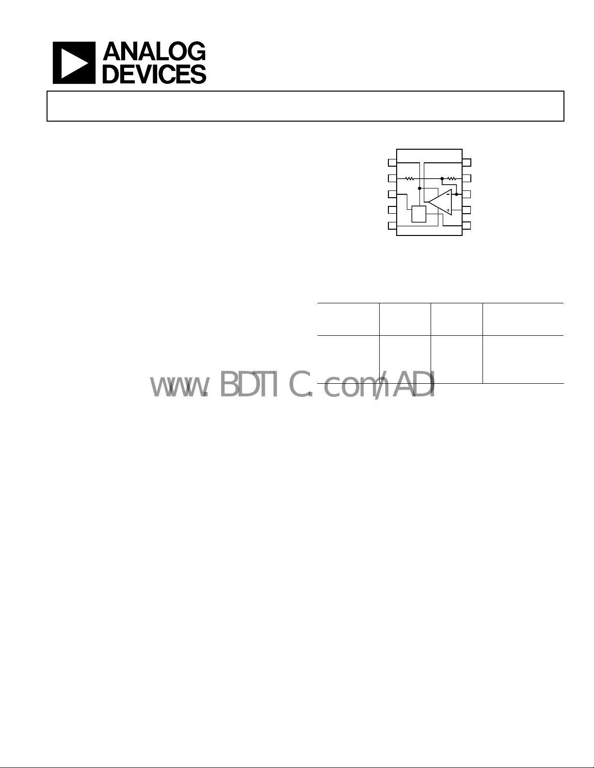
FUNCTIONAL BLOCK DIAGRAM
ADR821/ADR827
1
V+
R
2
1
3
4
5
NC = NO CONNECT
1
REF
Figure 1.
R
ND
NC
V–
Table 1. Selection Table
Reference
Part No.
V
OUT
ADR827ARMZ 1.25 V ±0.4% 30 ppm/°C
ADR827BRMZ 1.25 V ±0.2% 15 ppm/°C
ADR821ARMZ 2.50 V ±0.4% 30 ppm/°C
ADR821BRMZ 2.50 V ±0.2% 15 ppm/°C
10
R
2
9
8
7
6
Reference
Accuracy
AMP_OUT
R
2
–IN
+IN
REF_OUT
Reference
Temperature
Coefficient
06665-001
APPLICATIONS
Battery-powered instrumentation
Portable medical instrumentation
Data acquisition systems
Industrial process controls
Automotive applications
GENERAL DESCRIPTION
The ADR821/ADR827 combines a precision voltage reference
and an op amp in a 10-lead mini small outline package (MSOP).
The reference and the op amp can be operated independently,
offering the user a range of flexibility when arranging the
combination. Featuring a combined operating current of less
than 400 μA and 15 ppm/°C temperature drift on the reference,
the ADR821/ADR827 are ideally suited for applications requiring precision and low power.
Rev. 0
Information furnished by Analog Devices is believed to be accurate and reliable. However, no
responsibility is assumed by Anal og Devices for its use, nor for any infringements of patents or ot her
rights of third parties that may result from its use. Specifications subject to change without notice. No
license is granted by implication or otherwise under any patent or patent rights of Analog Devices.
Trademarks and registered trademarks are the property of their respective owners.
Available with the reference at 1.25 V and at 2.5 V, the
ADR821/ADR827 also come in two grades. The reference on
the A grade offers 30 ppm/°C temperature drift performance
and ±0.4% initial accuracy. The B grade provides a tighter
temperature drift performance of 15 ppm/°C and only ±0.2%
initial accuracy. All versions operate from −40°C to +125°C.
One Technology Way, P.O. Box 9106, Norwood, MA 02062-9106, U.S.A.
Tel: 781.329.4700 www.analog.com
Fax: 781.461.3113 ©2007 Analog Devices, Inc. All rights reserved.
Page 2

ADR821/ADR827
www.BDTIC.com/ADI
TABLE OF CONTENTS
Features.............................................................................................. 1
Absolute Maximum Ratings ............................................................9
Applications....................................................................................... 1
Functional Block Diagram .............................................................. 1
General Description ......................................................................... 1
Revision History ............................................................................... 2
Specifications..................................................................................... 3
ADR821 Electrical Characteristics—Reference ....................... 3
ADR821 Electrical Characteristics—Amplifier
(V
= ±2.8 V)................................................................................. 4
S
ADR821 Electrical Characteristics—Amplifier
(V
= ±15 V).................................................................................. 5
S
ADR827 Electrical Characteristics—Reference ....................... 6
ADR827 Electrical Characteristics—Amplifier
(V
= ±2.7 V)................................................................................. 7
S
ADR827 Electrical Characteristics—Amplifier
(V
= ±15 V).................................................................................. 8
S
REVISION HISTORY
Thermal Resistance.......................................................................9
ESD Caution...................................................................................9
Pin Configuration and Function Descriptions........................... 10
Typical Performance Characteristics........................................... 11
Reference ..................................................................................... 11
Amplifier (AD821/AD827)....................................................... 15
Applications Information.............................................................. 18
+2.5 V and −2.5 V Outputs (ADR821) ................................... 18
2.5 V and 5.0 V Outputs (ADR821)......................................... 18
Multiple 2.5 V Outputs (ADR821)........................................... 18
Outline Dimensions....................................................................... 19
Ordering Guide .......................................................................... 19
10/07—Revision 0: Initial Version
Rev. 0 | Page 2 of 20
Page 3
ADR821/ADR827
www.BDTIC.com/ADI
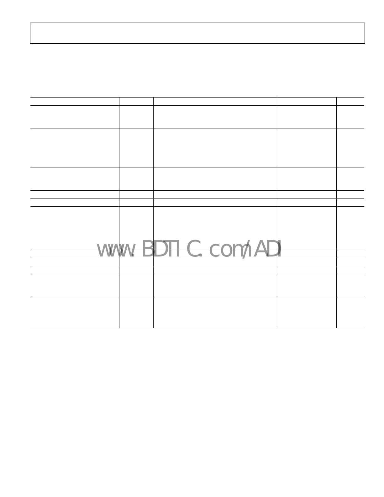
SPECIFICATIONS
ADR821 ELECTRICAL CHARACTERISTICS—REFERENCE
VIN = 2.8 V to 15 V, TA = 25°C, C
Table 2.
Parameter Symbol Conditions Min Typ Max Unit
OUTPUT VOLTAGE V
A Grade 2.490 2.500 2.510 V
B Grade 2.495 2.500 2.505 V
INITIAL ACCURACY V
A Grade 10 mV
0.40 %
B Grade 5.00 mV
0.20 %
TEMPERATURE COEFFICIENT TCV
A Grade 30 ppm/°C
B Grade 15 ppm/°C
DROPOUT (V
– VIN) VDO I
OUT
LINE REGULATION ∆V
LOAD REGULATION ∆V
I
I
VOLTAGE NOISE e
BROADBAND NOISE 10 Hz to 10 kHz 430 μV p-p
TURN-ON SETTLING TIME tR C
POWER SUPPLY
Positive Supply Current I
Negative Supply Current I
ON-BOARD RESISTORS R1, R2
Resistor Tolerance 8 10 12 kΩ
Resistor Matching 0.5 %
Resistor Temperature Coefficient TC ±100 ppm/°C
= C
IN
= 0.1 μF, unless otherwise noted.
OUT
OUT
OERR
−40°C < TA < +125°C
OUT
= 0 mA 0.3 V
OUT
/∆VIN VIN = 2.8 V to 15 V, −40°C < TA < +125°C 20 50 ppm/V
OUT
/∆I
= 0 mA to 5 mA, −40°C < TA < +125°C,
LOAD
I
LOAD
V
= 5 V
IN
= 0 mA to 5 mA, VIN = 5 V 80 200 ppm/mA
LOAD
= −3 mA to 0 mA, −40°C < TA < +125°C,
I
LOAD
V
= 5 V
IN
= −3 mA to +5 mA, VIN = 5 V 80 300 ppm/mA
LOAD
= 0 μF 80 μs
IN
OUT
0.1 Hz to 10 Hz 16 μV p-p
N p-p
No load, −40°C < TA < +125°C 400 μA
SY+
No load, −40°C < TA < +125°C 300 μA
SY−
400 ppm/mA
600 ppm/mA
Rev. 0 | Page 3 of 20
Page 4
ADR821/ADR827
www.BDTIC.com/ADI
ADR821 ELECTRICAL CHARACTERISTICS—AMPLIFIER (VS = ±2.8 V)
VCM = 0 V, TA = 25°C, unless otherwise noted.
Table 3.
Parameter Symbol Conditions Min Typ Max Unit
INPUT CHARACTERISTICS
Input Offset Voltage VOS −40°C < TA < +125°C 100 500 μV
Input Offset Voltage Drift TCVOS −40°C < TA < +125°C 2 5 μV/°C
Input Bias Current IB −40°C < TA < +125°C 15 50 nA
Input Offset Bias Current IOS −40°C < TA < +125°C 5 25 nA
Large Signal Voltage Gain AVO V
R
R
Common-Mode Rejection Ratio CMRR VCM = −1.5 V to +1.5 V, −40°C < TA < +125°C 75 100 dB
85 dB
OUTPUT CHARACTERISTICS
Output Voltage High VOH I
I
Output Voltage Low VOL I
I
POWER SUPPLY
Positive Supply Current I
Negative Supply Current I
No load, −40°C < TA < +125°C 400 μA
SY+
No load, −40°C < TA < +125°C 300 μA
SY−
Power Supply Rejection Ratio PSRR VS = ±2.8 V to ±15 V 75 100 dB
DYNAMIC PERFORMANCE
Slew Rate SR R
Gain Bandwidth Product GBP C
Phase Margin φM C
NOISE PERFORMANCE
Voltage Noise e
f = 0.1 Hz to 10 Hz 0.2 μV p-p
N p-p
Voltage Noise Density eN f = 1 kHz 16 nV/√Hz
= −1.5 V to +1.5 V
OUT
= 10 kΩ, −40°C < TA < +125°C 99 108 dB
LOAD
= 2 kΩ, −40°C < TA < +125°C 94 100 dB
LOAD
= 1 mA 2.6 2.7 V
LOAD
= 1 mA, −40°C < TA < +125°C 2.55 V
LOAD
= 1 mA −2.7 −2.6 V
LOAD
= 1 mA, −40°C < TA < +125°C −2.55 V
LOAD
= 10 kΩ, C
LOAD
= 14 pF 1.0 MHz
LOAD
= 14 pF 72.5 Degrees
LOAD
= 10 pF, AV = +1 0.5 V/μs
LOAD
Rev. 0 | Page 4 of 20
Page 5
ADR821/ADR827
www.BDTIC.com/ADI
ADR821 ELECTRICAL CHARACTERISTICS—AMPLIFIER (VS = ±15 V)
VCM= 0 V, TA = 25°C, unless otherwise noted.
Table 4.A
Parameter Symbol Conditions Min Typ Max Unit
INPUT CHARACTERISTICS
Input Offset Voltage VOS −40°C < TA < +125°C 100 500 μV
Input Offset Voltage Drift TCVOS −40°C < TA < +125°C 2 5 μV/oC
Input Bias Current IB −40°C < TA < +125°C 10 50 nA
Input Offset Bias Current IOS −40°C < TA < +125°C 5 25 nA
Large Signal Voltage Gain AVO V
R
R
Common-Mode Rejection Ratio CMRR VCM = −14 V to +14 V, −40°C < TA < +125°C 75 100 dB
85 dB
OUTPUT CHARACTERISTICS
Output Voltage high VOH I
I
Output Voltage Low VOL I
I
Output Current ISC Short-circuit current ±20 mA
POWER SUPPLY
Positive Supply Current I
Negative Supply Current I
No load, −40°C < TA < +125°C 400 μA
SY+
No load, −40°C < TA < +125°C 300 μA
SY−
Power Supply Rejection Ratio PSRR VS = ±2.8 V to ±15 V 75 100 dB
DYNAMIC PERFORMANCE
Slew Rate SR R
Gain Bandwidth Product GBP C
Phase Margin φM C
NOISE PERFORMANCE
Voltage Noise e
f = 0.1 Hz to 10 Hz 0.2 μV p-p
N p-p
Voltage Noise Density eN f = 1 kHz 16 nV/√Hz
= −14 V to +14 V
OUT
= 10 kΩ, −40°C < TA < +125°C 109.5 118 dB
LOAD
= 2 kΩ, −40°C < TA < +125°C 100 111 dB
LOAD
= 1 mA 14.8 14.9 V
LOAD
= 1 mA, −40°C < TA < +125°C 14.75 V
LOAD
= 1 mA −14.9 −14.8 V
LOAD
= 1 mA, −40°C < TA < +125°C −14.75 V
LOAD
= 10 kΩ, C
LOAD
= 14 pF 1.0 MHz
LOAD
= 14 pF 75.4 Degrees
LOAD
= 10 pF, AV = +1 0.5 V/μs
LOAD
Rev. 0 | Page 5 of 20
Page 6
ADR821/ADR827
www.BDTIC.com/ADI
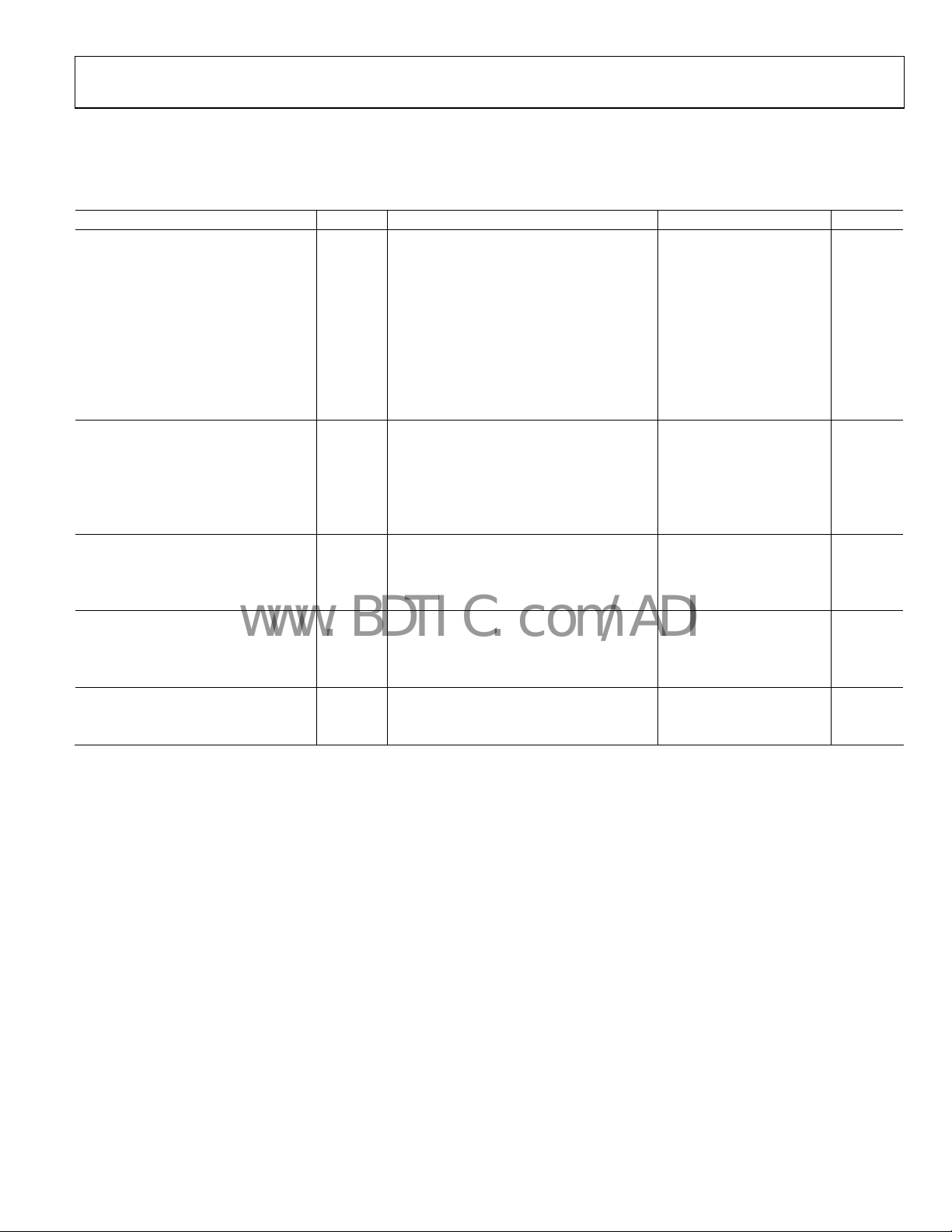
ADR827 ELECTRICAL CHARACTERISTICS—REFERENCE
VIN = 2.7 V to 15 V, TA = 25°C, C
Table 5.
Parameter Symbol Conditions Min Typ Max Unit
OUTPUT VOLTAGE V
A Grade
B Grade 1.2475 1.250 1.2525 V
INITIAL ACCURACY V
A Grade
0.40 %
B Grade 2.50 mV
0.20 %
TEMPERATURE COEFFICIENT TCV
A Grade 30 ppm/°C
B Grade 15 ppm/°C
DROPOUT (V
– VIN) V
OUT
LINE REGULATION ∆V
LOAD REGULATION ∆V
I
I
VOLTAGE NOISE e
BROADBAND NOISE 10 Hz to 10 kHz 260 μV p-p
TURN-ON SETTLING TIME tR C
POWER SUPPLY
Positive Supply Current I
Negative Supply Current I
ON-BOARD RESISTORS R1, R2
Resistor Tolerance 8 10 12 kΩ
Resistor Matching 0.5 %
Resistor Temperature Coefficient TC ±100 ppm/°C
= C
IN
= 0.1 μF, unless otherwise noted.
OUT
OUT
OERR
OUT
DO
/∆VIN VIN = 2.7 V to 15 V, −40°C < TA < +125°C 20 50 ppm/V
OUT
/∆I
OUT
0.1 Hz to 10 Hz 8 μV p-p
N p-p
No load, −40°C < TA < +125°C 400 μA
SY+
No load, −40°C < TA < +125°C 300 μA
SY−
1.245 1.250 1.255 V
5 mV
−40°C < TA < +125°C
I
= 0 mA 1.45 V
OUT
LOAD
= 0 mA to 5 mA, −40°C < TA < +125°C,
I
LOAD
V
= 3 V
IN
= 0 mA to 5 mA, VIN = 3 V 80 200 ppm/mA
LOAD
= −3 mA to 0 mA, −40°C < TA < +125°C,
I
LOAD
V
= 3 V
IN
= −3 mA to +5 mA, VIN = 3 V 80 300 ppm/mA
LOAD
= 0 μF, C
IN
= 0.1 μF 80 μs
OUT
400 ppm/mA
600 ppm/mA
Rev. 0 | Page 6 of 20
Page 7

ADR821/ADR827
www.BDTIC.com/ADI
ADR827 ELECTRICAL CHARACTERISTICS—AMPLIFIER (VS = ±2.7 V)
VCM = 0 V, TA = 25°C, unless otherwise noted.
Table 6.
Parameter Symbol Conditions Min Typ Max Unit
INPUT CHARACTERISTICS
Input Offset Voltage VOS −40°C < TA < +125°C 100 500 μV
Input Offset Voltage Drift TCVOS −40°C < TA < +125°C 2 5 μV/°C
Input Bias Current IB −40°C < TA < +125°C 15 50 nA
Input Offset Bias Current IOS −40°C < TA < +125°C 5 25 nA
Large Signal Voltage Gain AVO V
R
R
Common-Mode Rejection Ratio CMRR VCM = −1.5 V to +1.5 V, −40°C < TA < +125°C 75 100 dB
85 dB
OUTPUT CHARACTERISTICS
Output Voltage High VOH I
I
Output Voltage Low VOL I
I
POWER SUPPLY
Positive Supply Current I
Negative Supply Current I
No load, −40°C < TA < +125°C 400 μA
SY+
No load, −40°C < TA < +125°C 300 μA
SY−
Power Supply Rejection Ratio PSRR VS = ±2.7 V to ±15 V 75 100 dB
DYNAMIC PERFORMANCE
Slew Rate SR R
Gain Bandwidth Product GBP C
Phase Margin φM C
NOISE PERFORMANCE
Voltage Noise e
f = 0.1 Hz to 10 Hz 0.2 μV p-p
N p-p
Voltage Noise Density eN f = 1 kHz 16 nV/√Hz
= −1.5 V to +1.5 V
OUT
= 10 kΩ, −40°C < TA < +125°C 99 108 dB
LOAD
= 2 kΩ, −40°C < TA < +125°C 94 100 dB
LOAD
= 1 mA 2.5 2.6 V
LOAD
= 1 mA, −40°C < TA < +125°C 2.45 V
LOAD
= 1 mA −2.6 −2.5 V
LOAD
= 1 mA, −40°C < TA < +125°C −2.45 V
LOAD
= 10 kΩ, C
LOAD
= 14 pF 1.0 MHz
LOAD
= 14 pF 71.3 Degrees
LOAD
= 10 pF, AV = +1 0.5 V/μs
LOAD
Rev. 0 | Page 7 of 20
Page 8

ADR821/ADR827
www.BDTIC.com/ADI
ADR827 ELECTRICAL CHARACTERISTICS—AMPLIFIER (VS = ±15 V)
VCM = 0 V, TA = 25°C, unless otherwise noted.
Table 7.
Parameter Symbol Conditions Min Typ Max Unit
INPUT CHARACTERISTICS
Input Offset Voltage VOS −40°C < TA < +125°C 100 500 μV
Input Offset Voltage Drift TCVOS −40°C < TA < +125°C 2 5 μV/°C
Input Bias Current IB −40°C < TA < +125°C 10 50 nA
Input Offset Bias Current IOS −40°C < TA < +125°C 5 25 nA
Large Signal Voltage Gain AVO V
R
R
Common-Mode Rejection Ratio CMRR VCM = −14 V to +14 V, −40°C < TA < 125°C 75 100 dB
85 dB
OUTPUT CHARACTERISTICS
Output Voltage High VOH I
I
Output Voltage Low VOL I
I
Output Current ISC Short-circuit current ±20 mA
POWER SUPPLY
Positive Supply Current I
Negative Supply Current I
No load, −40°C < TA < +125°C 400 μA
SY+
No load, −40°C < TA < +125°C 300 μA
SY−
Power Supply Rejection Ratio PSRR VS = ±2.7 V to ±15 V 75 100 dB
DYNAMIC PERFORMANCE
Slew Rate SR R
Gain Bandwidth Product GBP C
Phase Margin φM C
NOISE PERFORMANCE
Voltage Noise e
f = 0.1 Hz to 10 Hz 0.2 μV p-p
N p-p
Voltage Noise Density eN f = 1 kHz 16 nV/√Hz
= −14 V to +14 V
OUT
= 10 kΩ, −40°C < TA < +125°C 109.5 118 dB
LOAD
= 2 kΩ, −40°C < TA < +125°C 100 111 dB
LOAD
= 1 mA 14.8 14.9 V
LOAD
= 1 mA, −40°C < TA < +125°C 14.75 V
LOAD
= 1 mA −14.9 −14.8 V
LOAD
= 1 mA, −40°C < TA < +125°C −14.75 V
LOAD
= 10 kΩ, C
LOAD
= 14 pF 1.0 MHz
LOAD
= 14 pF 75.4 Degrees
LOAD
= 10 pF, AV = +1 0.5 V/μs
LOAD
Rev. 0 | Page 8 of 20
Page 9

ADR821/ADR827
www.BDTIC.com/ADI
ABSOLUTE MAXIMUM RATINGS
TA= 25°C, unless otherwise noted.
Table 8.
Parameter Rating
Supply Voltage ±18 V
Output Short-Circuit Duration to GND Indefinite
Storage Temperature Range –65°C to +125°C
Operating Temperature Range –40°C to +125°C
Junction Temperature Range –65°C to +125°C
Lead Temperature (Soldering, 60 sec) 300°C
Stresses above those listed under Absolute Maximum Ratings
may cause permanent damage to the device. This is a stress
rating only; functional operation of the device at these or any
other conditions above those indicated in the operational
section of this specification is not implied. Exposure to absolute
maximum rating conditions for extended periods may affect
device reliability.
THERMAL RESISTANCE
θJA is specified for the worst-case conditions, that is, θJA is
specified for device soldered in circuit board for surface-mount
packages.
Table 9. Thermal Resistance
Package Type θJA θ
10-Lead MSOP (RM-10) 172 50 °C/W
Unit
JC
ESD CAUTION
Rev. 0 | Page 9 of 20
Page 10

ADR821/ADR827
G
www.BDTIC.com/ADI
PIN CONFIGURATION AND FUNCTION DESCRIPTIONS
V+
1
R
2
1
ADR821/
3
ND
ADR827
TOP VIEW
4
NC
(Not to Scale)
V–
5
NC = NO CONNECT
Figure 2. Pin Configuration
Table 10. Pin Function Descriptions
Pin No. Mnemonic Description
1 V+ Input Voltage of the Reference/Positive Supply of the Amplifier
2 R1 Resistance Tied to Positive Input of the Amplifier
3 GND Ground
4 NC Do Not Connect Any External Components to This Pin
5 V− Negative Supply of the Amplifier
6 REF_OUT Output Voltage of the Reference
7 +IN Positive Input of the Amplifier
8 −IN Negative Input of the Amplifier
9 R2 Resistance Tied to Positive Input of the Amplifier
10 AMP_OUT Output Pin of the Amplifier
AMP_OUT
10
R
9
8
–IN
7
+IN
REF_OUT
6
2
6665-002
Rev. 0 | Page 10 of 20
Page 11

ADR821/ADR827
www.BDTIC.com/ADI
TYPICAL PERFORMANCE CHARACTERISTICS
REFERENCE
2.512
CIN = 0.1µF
= 0.1µF
C
OUT
V
= 15V
IN
2.508
2.504
(V)
2.500
OUT
V
2.496
2.492
2.488
–40 125
–25 –10 5 20 35 50 65 80 95 110
TEMPERATURE (° C)
Figure 3. ADR821 V
vs. Temperature
OUT
06665-005
1.260
CIN = 0.1µF
= 0.1µF
C
OUT
1.258
= 15V
V
IN
1.256
1.254
1.252
(V)
1.250
OUT
V
1.248
1.246
1.244
1.242
1.240
–40 125
–25–105 203550658095110
TEMPERATURE (° C)
Figure 6. ADR827 V
vs. Temperature
OUT
06665-008
4
3
2
1
0
LINE REGULATION (ppm/V)
–1
–2
–40 –25 –10 5 20 35 50 65 80 95 110
TEMPERATURE (° C)
Figure 4. ADR821 Line Regulation vs. Temperature
0.40
0.35
0.30
0.25
(mA)
SY+
0.20
I
0.15
0.10
+125°C
+25°C
–40°C
CIN = 0.1µF
= 0.1µF
C
OUT
V
= 15V
IN
CIN = 0.1µF
= 0.1µF
C
OUT
125
14
12
10
8
6
4
LINE REGULATION (ppm/V)
2
0
–40 –25 –10 5 20 35 50 65 80 95 110
06665-006
TEMPERATURE (° C)
CIN = 0.1µF
= 0.1µF
C
OUT
= 15V
V
IN
125
06665-009
Figure 7. ADR827 Line Regulation vs. Temperature
0.40
CIN = 0.1µF
= 0.1µF
C
OUT
0.35
0.30
0.25
(mA)
0.20
SY+
I
0.15
0.10
0.05
+125°C
+25°C
–40°C
0.05
2.5 15.0
5.0 7.5 10.0 12.5
SUPPLY VOLTAGE (±V)
06665-007
Figure 5. ADR821 Supply Current (+) vs. Supply Voltage
Rev. 0 | Page 11 of 20
0
2.5 15.0
5.0 7.5 10.0 12.5
SUPPLY VOLTAGE (±V)
Figure 8. ADR827 Supply Current (+) vs. Supply Voltage
06665-010
Page 12

ADR821/ADR827
www.BDTIC.com/ADI
0.25
0.20
CIN = 0.1µF
= 0.1µF
C
OUT
+125°C
0.25
0.20
CIN = 0.1µF
= 0.1µF
C
OUT
+125°C
0.15
(mA)
SY–
I
0.10
0.05
0
2.5 15.0
5.0 7.5 10.0 12.5
+25°C
–40°C
SUPPLY VOLTAGE (±V)
Figure 9. ADR821 Supply Current (−) vs. Supply Voltage
1.2
CIN = 0.1µF
= 0.1µF
C
OUT
1.0
0.8
0.6
DROPOUT (V)
0.4
0.2
0
–3 7
–2–10123456
LOAD CURRENT (mA)
+125°C
+25°C
–40°C
Figure 10. ADR821 Dropout vs. Load Current
0.15
(mA)
SY–
I
0.10
0.05
0
2.5 15.0
06665-011
5.0 7.5 10.0 12.5
+25°C
–40°C
SUPPLY VOLTAGE (±V)
06665-014
Figure 12. ADR827 Supply Current (−) vs. Supply Voltage
2.0
CIN = 0.1µF
= 0.1µF
C
OUT
1.8
1.6
1.4
1.2
1.0
0.8
DROPOUT (V)
0.6
0.4
0.2
0
–3 7
06665-012
–40°C
+25°C
+125°C
–2 –1 0 1 2 3 4 5 6
LOAD CURRENT (mA)
06665-015
Figure 13. ADR827 Dropout vs. Load Current
50
I
= 3mA
SINK
C
= C
= 0.1µF
IN
45
40
35
30
25
20
15
LOAD REGULATION (ppm/mA)
10
5
OUT
VS = 5V
VS = 15V
–40 –25 –10 5 20 35 50 65 80 95 110 125
TEMPERATURE (° C)
Figure 11. ADR821 Load Regulation vs. Temperature
06665-013
Rev. 0 | Page 12 of 20
80
I
= 3mA
SINK
C
= C
= 0.1µF
IN
OUT
70
60
50
LOAD REGULATION (ppm/mA)
40
30
–40 –25 –10 5 20 35 50 65 80 95 110 125
VS = 15V
VS = 3V
TEMPERATURE (° C)
Figure 14. ADR827 Load Regulation vs. Temperature
06665-016
Page 13

ADR821/ADR827
www.BDTIC.com/ADI
0
I
= 5mA
SOURCE
= C
C
–20
–40
–60
–80
–100
LOAD REGULATION (ppm/mA)
–120
–140
–40 125
= 0.1µF
IN
OUT
VS = 5V
VS = 15V
–25 –10 5 20 35 50 65 80 95 110
TEMPERATURE (° C)
Figure 15. ADR821 Load Regulation vs. Temperature
10µV/DIV
1
CIN = C
15.6µV p-p
2.78µV rms
OUT
= 0.1µF
06665-017
0
I
= 5mA
SOURCE
C
= C
= 0.1µF
IN
–20
–40
–60
–80
–100
LOAD REGULATION (ppm/mA)
–120
–140
OUT
VS = 3V
VS = 15V
–40 125
–25 –10 5 20 35 50 65 80 95 110
TEMPERATURE (° C)
Figure 18. ADR827 Load Regulation vs. Temperature
5µV/DIV
1
CIN = C
8.3µV p-p
1.33µV rms
OUT
= 0.1µF
06665-020
100µV/DIV
TIME (1s/ DIV)
Figure 16. ADR821 0.1 Hz to 10 Hz Noise
1
CIN = C
426µV p-p
55.6µV rms
OUT
= 0.1µF
TIME (1s/ DIV)
Figure 17. ADR821 10 Hz to 10 kHz Noise
06665-018
TIME (1s/ DIV)
06665-021
Figure 19. ADR827 0.1 Hz to 10 Hz Noise
CIN = C
258µV p-p
34.6µV rms
1
100µV/DIV
06665-019
OUT
= 0.1µF
TIME (1s/ DIV)
06665-022
Figure 20. ADR827 10 Hz to 10 kHz Noise
Rev. 0 | Page 13 of 20
Page 14

ADR821/ADR827
www.BDTIC.com/ADI
CHANNEL 2:
V
= 1V/DIV
OUT
2
CHANNEL 1:
V
= 2V/DIV
IN
C
= 0µF
IN
C
1
= 0.1µF
L
TIME = 20µ s/DIV
6665-023
Figure 21. ADR821 Turn-On Response
2
1
Figure 22. ADR827 Turn-On Response
CHANNEL 2:
V
= 500mV/DIV
OUT
CHANNEL 1:
V
= 2V/DIV
IN
C
= 0µF
IN
C
= 0.1µF
L
TIME = 20µ s/DIV
6665-024
Rev. 0 | Page 14 of 20
Page 15

ADR821/ADR827
www.BDTIC.com/ADI
AMPLIFIER (AD821/AD827)
120
VSY = ±15V
T
= 25°C
A
100
80
60
40
NUMBER OF SAMPLES
20
0
–500 –400 –300 –200 –100 0 100 200 300 400 500
V
(µV)
OS
Figure 23. Input Offset Voltage Distribution
06665-025
500
VSY = ±15V
T
= 25°C
A
400
300
200
100
(µV)
0
OS
V
–100
–200
–300
–400
–500
–15 15
–12–9–6–3036912
V
(V)
CM
Figure 26. Input Offset Voltage vs. Common-Mode Voltage
06665-029
160
VSY = ±15V
140
120
100
80
60
NUMBER OF SAMPLE S
40
20
0
–5 –4 –3 –2 –1 0 1 2 3 4 5
(µV/°C)
TCV
OS
Figure 24. Offset Voltage Drift Distribution
60
VSY = ±15V
50
= 25°C
T
A
40
30
20
10
(nA)
B
I
0
–10
–20
–30
–40
–13 –11 –9 –7 –5 –3 –1 1 3 5 7 9 11 13
V
(V)
CM
Figure 25. Input Bias Current vs. Common-Mode Voltage
200
100
(µV)
0
OS
V
–100
–200
–55 155
–40 –25 –10 5 20 35 50 65 80 95 110 125 140
06665-026
TEMPERATURE (° C)
VSY = ±15V
06665-027
Figure 27. Input Offset Voltage vs. Temperature
100000
VSY = ±15V
= 25°C
T
A
10000
1000
VOL SINKING
100
10
1
OUTPUT SWING SATURATION VOLTAGE (mV)
0.1
0.01 100
06665-030
VSY – VOH SOURCING
0.1 1 10
LOAD CURRENT (mA)
06665-028
Figure 28. Output Swing Saturation Voltage vs. Load Current
Rev. 0 | Page 15 of 20
Page 16

ADR821/ADR827
V
www.BDTIC.com/ADI
70
50
30
10
GAIN (dB)
–10
–30
–50
100 100M
1k 10k 100k 1M 10M
PHASE
GAIN
FREQUENCY (Hz)
VSY = ±15V
T
A
Figure 29. Open-Loop Gain and Phase vs. Frequency
= 25°C
120
105
90
75
60
45
30
15
0
–15
–30
–45
–60
PHASE (Degrees)
06665-031
140
120
100
80
60
CMRR (dB)
40
20
0
100 100M
1k 10k 100k 1M 10M
FREQUENCY (Hz)
VSY = ±15V
T
= 25°C
A
Figure 32. CMRR vs. Frequency
06665-034
50
G = 100
40
30
G = 10
20
10
G = 1
0
(dB)
CL
–10
A
–20
–30
–40
–50
–60
100 100M
1k 10k 100k 1M 10M
FREQUENCY (Hz)
VSY = ±15V
T
A
Figure 30. Closed-Loop Gain vs. Frequency
1200
VSY = ±15V
= 25°C
T
A
1000
800
()
600
OUT
Z
400
= 25°C
140
120
100
80
60
PSRR (dB)
40
20
0
100 100M
06665-032
1k 10k 100k 1M 10M
FREQUENCY (Hz)
PSRR–
VSY = ±15V
= 25°C
T
A
PSRR+
06665-035
Figure 33. PSRR vs. Frequency
R
= 10k
LOAD
C
= 10pF
LOAD
V
= ±15V
SY
2
= 2V/DI
OUT
V
200
G = 100 G = 10 G = 1
0
10 10M
100 1k 10k 100k 1M
FREQUENCY (Hz)
Figure 31. Z
vs. Frequency
OUT
06665-033
Rev. 0 | Page 16 of 20
TIME = 10µs/DIV
Figure 34. Large Signal Transient Response
06665-036
Page 17

ADR821/ADR827
V
V
www.BDTIC.com/ADI
RL = 10k
C
= 10pF
L
V
= ±15V
SY
2
= 50mV/DI
OUT
V
TIME = 1µs/DIV
Figure 35. Small Signal Transient Response, C
= 10 pF
L
1000
100
EN (nV/ Hz)
10
1
06665-037
1 10000
10 100 1000
FREQUENCY (Hz)
Figure 37. Voltage Noise Density
VSY = ±15V
T
= 25°C
A
06665-039
RL = 10k
C
= 100pF
V
L
= ±15V
SY
2
= 50mV/DI
OUT
V
TIME = 1µs/DIV
Figure 36. Small Signal Transient Response, C
= 100 pF
L
06665-038
Rev. 0 | Page 17 of 20
Page 18

ADR821/ADR827
www.BDTIC.com/ADI
APPLICATIONS INFORMATION
+2.5 V AND −2.5 V OUTPUTS (ADR821)
REF_OUT
REF
V+
+IN
R
1
Figure 38. +2.5 V and −2.5 V Outputs
V–
10k10k
AMP_OUT
R
In many dual-supply applications, it is desirable to have ±2.5 V
references. Using the configuration shown in Figure 38, it is
possible to generate −2.5 V with the help of a +2.5 V reference,
an internal op amp, and 10 kΩ resistors. The supply voltages V+
and V− should be greater than +2.8 V and −2.8 V, respectively.
The op amp is configured as an inverting amplifier with a gain
of −1, which produces −2.5 V at the output of the op amp. The
output of the reference is fed to the amplifier inverting input.
Because the op amp has very low input offset voltage (500 μV
over the full temperature range) and the TC ratio of the
resistors is typically ±25 ppm/°C, the −2.5 V output is less than
7 mV away from the theoretical value.
0.1µF
2
+2.5V
–2.5V
6665-003
2.5 V AND 5.0 V OUTPUTS (ADR821)
REF_OUT
REF
V+
+IN
R
1
Figure 39. 2.5 V and 5.0 V Outputs
V–
–IN
10k10k
AMP_OUT
R
In many single-supply applications, it is desirable to have
multiple reference voltages. Using the configuration shown in
Figure 39, it is possible to generate 5.0 V with the help of a
2.5 V reference, an internal op amp, and resistors. V+ should
be kept at greater than 5.8 V and V− can be connected either
to ground or to negative supply. The output of the reference is
0.1µF
2
2.5V
5.0V
06665-004
fed to the amplifier noninverting input. The op amp is configured as a noninverting amplifier with a gain of +2, which
produces 5 V at the output of the op amp. Using the guaranteed
maximum offset voltage over the temperature, and the typical
TC ratio of the resistors over the full temperature range, the
output is within 15 mV of the calculated value.
MULTIPLE 2.5 V OUTPUTS (ADR821)
REF_OUT
REF
V+
+IN
R
1
Figure 40. Multiple 2.5 V Outputs
V–
–IN
AMP_OUT
10k10k
On some boards, sensitive analog circuits, such as a VCO, exist
with noisy digital circuits. If the supply current requirements
are low (less than 3 mA), series references and op amps can be
used. Using the configuration shown in Figure 40, two different
2.5 V supplies can be created using a single ADR821. The supply
voltage V+ should be greater than 2.8 V and V− can be connected to ground or a negative voltage. The op amp is configured
as a voltage follower with a gain of +1, which produces 2.5 V at
the output of the op amp. The output of the reference is fed
to the amplifier noninverting input. Because the op amp has
very low input offset voltage (500 μV maximum over the full
temperature range), the output voltage from the op amp section
tracks the reference voltage within 1 mV. For a dynamic load,
such as the reference input pin on some analog-to-digital
converters, the load should be connected to an op amp output
and the noise sensitive circuitry, such as a VCO, should be
connected to the reference output. If the dynamic load is connected to the reference voltage, any perturbations appear as a
signal to the input of the voltage follower and appear on the
other output.
0.1µF
2.5V
2.5V
R
2
06665-040
Rev. 0 | Page 18 of 20
Page 19

ADR821/ADR827
www.BDTIC.com/ADI
OUTLINE DIMENSIONS
3.10
3.00
2.90
6
10
3.10
3.00
2.90
1
PIN 1
0.50 BSC
0.95
0.85
0.75
0.15
0.05
0.33
0.17
COPLANARITY
0.10
COMPLIANT TO JEDEC STANDARDS MO-187-BA
Figure 41. 10-Lead Mini Small Outline Package [MSOP]
ORDERING GUIDE
Output
Models
Range
ADR821ARMZ-REEL71 −40°C to +125°C 2.500 10.00 ±0.40 30 10-Lead MSOP RM-10 1,000 R2G
ADR821ARMZ-R21 −40°C to +125°C 2.500 10.00 ±0.40 30 10-Lead MSOP RM-10 250 R2G
ADR821BRMZ-REEL71 −40°C to +125°C 2.500 5.00 ±0.20 15 10-Lead MSOP RM-10 1,000 R2H
ADR821BRMZ-R21 −40°C to +125°C 2.500 5.00 ±0.20 15 10-Lead MSOP RM-10 250 R2H
ADR827ARMZ-REEL71 −40°C to +125°C 1.250 5.00 ±0.40 30 10-Lead MSOP RM-10 1,000 R0Z
ADR827ARMZ-R21 −40°C to +125°C 1.250 5.00 ±0.40 30 10-Lead MSOP RM-10 250 R0Z
ADR827BRMZ-REEL71 −40°C to +125°C 1.250 2.50 ±0.20 15 10-Lead MSOP RM-10 1,000 R2B
Temperature
ADR827BRMZ-R2
1
Z = RoHS Compliant Part.
1
−40°C to +125°C 1.250 2.50 ±0.20 15 10-Lead MSOP RM-10 250 R2B
Voltage
(V
)
OUT
(mV) (%)
5.15
4.90
4.65
5
1.10 MAX
SEATING
PLANE
0.23
0.08
(RM-10)
Dimensions shown in millimeters
Initial
Accuracy
Temperature
Coefficient
(ppm/°C)
8°
0°
0.80
0.60
0.40
Package
Description
Package
Option
Ordering
Quantity Branding
Rev. 0 | Page 19 of 20
Page 20

ADR821/ADR827
www.BDTIC.com/ADI
NOTES
©2007 Analog Devices, Inc. All rights reserved. Trademarks and
registered trademarks are the property of their respective owners.
D06665-0-10/07(0)
Rev. 0 | Page 20 of 20
 Loading...