

Page 1
1.2 V Precision Low Noise
Shunt Voltage Reference
ADR512
FEATURES
Precision 1.200 V Voltage Reference
Ultracompact 3 mm 3 mm SOT-23 Package
No External Capacitor Required
Low Output Noise: 4 V p-p (0.1 Hz to 10 Hz)
Initial Accuracy: 0.3% Max
Temperature Coefficient: 60 ppm/C Max
Operating Current Range: 100 A to 10 mA
Output Impedance: 0.3 Max
Temperature Range: –40C to +85C
APPLICATIONS
Precision Data Acquisition Systems
Battery-Powered Equipment:
Cellular Phone, Notebook Computer, PDA,
and GPS
3 V/5 V, 8-/12-Bit Data Converters
Portable Medical Instruments
Industrial Process Control Systems
Precision Instruments
GENERAL DESCRIPTION
Designed for space critical applications, the ADR512 is a low
voltage (1.200 V), precision shunt-mode voltage reference in the
ultracompact (3 mm ⫻ 3 mm) SOT-23 package. The ADR512
features low temperature drift (60 ppm/⬚C), high accuracy
(⫾0.30%), and ultralow noise (4 V p-p) performance.
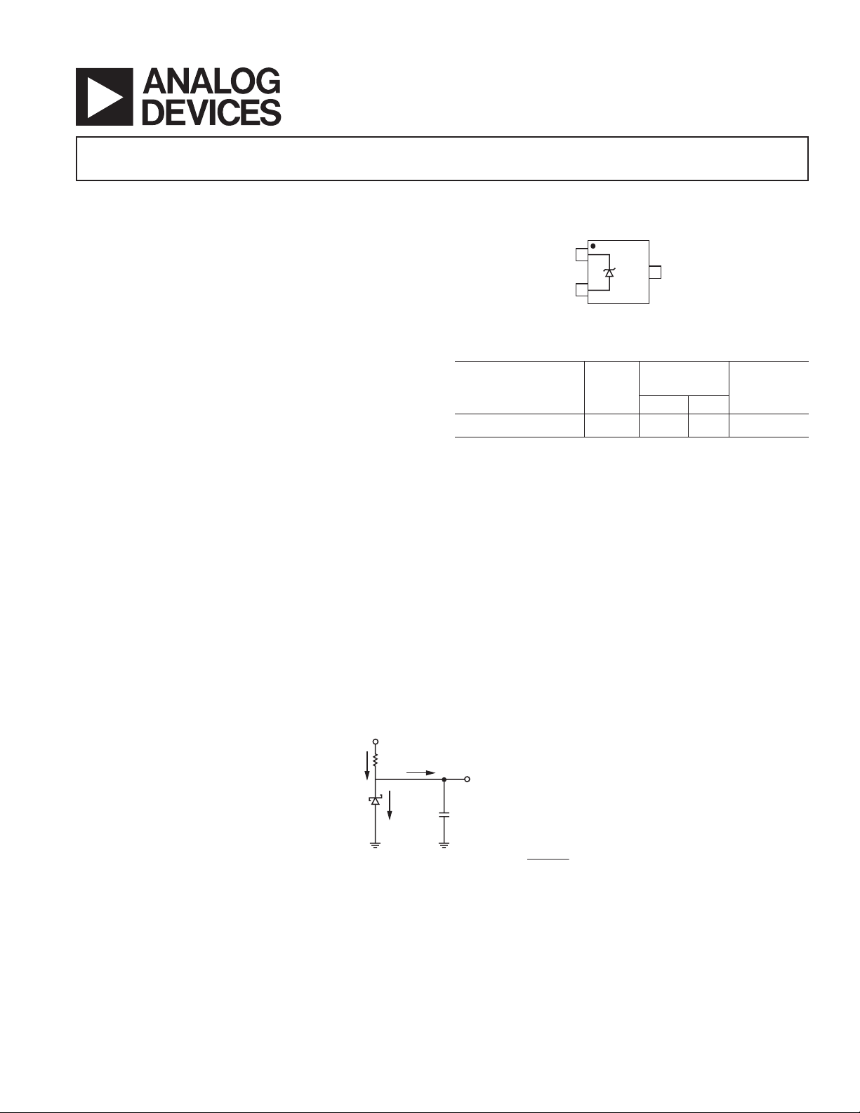
PIN CONFIGURATION
3-Lead SOT-23
ADR512
+
1
V
3
–
V
2
TRIM/NC
ADR512
Output Initial
Temperature
Voltage Accuracy Coefficient
Model (VO) (mV) (%) (ppm/C)
ADR512ART-REEL7 1.200 3.5 0.3 60
A TRIM terminal is available on the ADR512 to provide adjustment of the output voltage over ⫾0.5% without affecting the
temperature coefficient of the device. This feature provides
users with the flexibility to trim out any system errors.
The ADR512’s advanced design eliminates the need for an
external capacitor, yet it is stable with any capacitive load. The
minimum operating current increases from a scant 100 A to a
maximum of 10 mA. This low operating current and ease of use
make the ADR512 ideally suited for handheld battery-powered
applications.
V
S
R
IL + I
ADR512
BIAS
Q
I
Q
I
Figure 1. Typical Operating Circuit
REV. 0
Information furnished by Analog Devices is believed to be accurate and
reliable. However, no responsibility is assumed by Analog Devices for its
use, nor for any infringements of patents or other rights of third parties that
may result from its use. No license is granted by implication or otherwise
under any patent or patent rights of Analog Devices. Trademarks and
registered trademarks are the property of their respective companies.
L
V
= 1.2V
OUT
C
OUT
(OPTIONAL)
VS – V
R
BIAS
One Technology Way, P.O. Box 9106, Norwood, MA 02062-9106, U.S.A.
Tel: 781/329-4700 www.analog.com
Fax: 781/326-8703 © 2003 Analog Devices, Inc. All rights reserved.
OUT
=
IL + I
Q
Page 2
ADR512–SPECIFICATIONS
ELECTRICAL CHARACTERISTICS
(IIN = 100 A to 10 mA @ TA = 25C, unless otherwise noted.)
Parameter Symbol Conditions Min Typ Max Unit
Output Voltage
Initial Accuracy V
Temperature Coefficient A Grade TCV
Output Voltage Change vs. I
Dynamic Output Impedence (∆V
Minimum Operating Current I
Voltage Noise e
Turn-On Settling Time
Output Voltage Hysteresis V
NOTES
1
The forward diode voltage characteristic at –1 mA is typically 0.65 V.
2
Measured without a load capacitor.
Specifications subject to change without notice.
ABSOLUTE MAXIMUM RATINGS*
Reverse Current . . . . . . . . . . . . . . . . . . . . . . . . . . . . . . . 25 mA
Forward Current . . . . . . . . . . . . . . . . . . . . . . . . . . . . . . 20 mA
Storage Temperature Range
RT Package . . . . . . . . . . . . . . . . . . . . . . . . –65°C to +150°C
Operating Temperature Range . . . . . . . . . . . . –40°C to +85°C
Junction Temperature Range
1
IN
2
V
O
OERR
V
OERR%
O
∆V
R
/∆IR)IIN = 1 mA ±100 µA 0.3 Ω
R
IN
p-p f = 0.1 Hz to 10 Hz 4 µV p-p
N
t
R
O_HYS
–40°C < TA < +85°C60ppm/°C
IIN = 0.1 mA to 10 mA 3 mV
–40°C < TA < +85°C 100 µA
To within 0.1% of Output 10 µs
Package Type
1
1.1965 1.2 1.2035 V
–3.5 +3.5 mV
–0.3 +0.3 %
50 ppm
2
JA
JC
Unit
3-SOT-23 (RT) 230 146 °C/W
NOTES
1
Package power dissipation = (T
2
θJA is specified for worst-case conditions, i.e., θ
device soldered.
JMAX
– TA)/θJA.
is specified for
JA
RT Package . . . . . . . . . . . . . . . . . . . . . . . . –65°C to +150°C
Lead Temperature Range (Soldering, 60 Sec) . . . . . . . . 300°C
*Absolute maximum ratings apply at 25°C, unless otherwise noted. Stresses above
those listed under Absolute Maximum Ratings may cause permanent damage to
the device. This is a stress rating only; functional operation of the device at these
or any other conditions above those indicated in the operational section of this
specification is not implied. Exposure to absolute maximum rating conditions for
extended periods may affect device reliability.
ORDERING GUIDE
Output Initial Temperature Number
Voltage Accuracy Coefficient Package Package of Parts Temperature
Model (VO)(mV) (%) (ppm/C) Description Option Branding per Reel Range
ADR512ART-REEL7 1.2 3.5 0.3 60 SOT-23 RT-3 RGA 3,000 –40°C to +85°C
ADR512ART-R2 1.2 3.5 0.3 60 SOT-23 RT-3 RGA 250 –40°C to +85°C
CAUTION
ESD (electrostatic discharge) sensitive device. Electrostatic charges as high as 4000 V readily
accumulate on the human body and test equipment and can discharge without detection. Although the
ADR512 features proprietary ESD protection circuitry, permanent damage may occur on devices
subjected to high energy electrostatic discharges. Therefore, proper ESD precautions are recommended
to avoid performance degradation or loss of functionality.
REV. 0–2–
Page 3
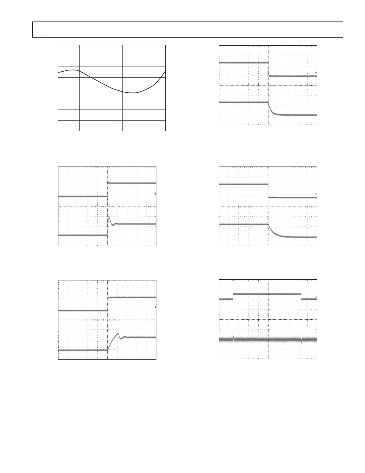
1.204
1.203
Typical Performance Characteristics–ADR512
1.202
1.201
(V)
1.200
OUT
V
1.199
1.198
1.197
1.196
TPC 1. Typical V
–15–40 10 35 60 85
TEMPERATURE (C)
vs. Temperature
OUT
VIN = 2V/DIV
V
= 1V/DIV
OUT
V
OUT
TIME (400s/DIV)
TPC 4. Turn Off Time
V
VIN = 2V/DIV
= 1V/DIV
VIN = 2V/DIV
= 1V/DIV
OUT
TIME (100s/DIV)
TPC 2. Turn On Time
VIN = 2V/DIV
V
= 1V/DIV
OUT
TIME (100s/DIV)
TPC 3. Turn On Time with 1 µF Input Capacitor
TIME (200s/DIV)
TPC 5. Turn Off Time with 1 µF Input Capacitor
∆IIN = 100A
V
= 20mV/DIV
OUT
TIME (2s/DIV)
TPC 6. Output Response to 100 µA Input Current Change
REV. 0
–3–
Page 4

ADR512
∆IIN = 100A
V
= 20mV/DIV
OUT
2V/DIV
TIME (2s/DIV)
TPC 7. Output Response to 100 µA Input Current
Change With 1 µF Capacitor
PARAMETER DEFINITIONS
Temperature Coefficient
This is the change of output voltage with respect to operating
temperature changes, normalized by the output voltage at 25°C.
This parameter is expressed in ppm/°C and can be determined
with the following equation:
TCV
where:
V
(25°C) = VO at 25°C
O
V
O(T1
V
O(T2
ppm
O
C
°
) = VO at Temperature 1
) = VO at Temperature 2
VT VT
()−()
OO
=
VCTT
21
°
×−
25
()
O
()
21
6
×
10
(1)
Thermal Hysteresis
Thermal hysteresis is defined as the change of output voltage
after the device is cycled through the temperature from +25°C to
–40°C to +85°C and back to +25°C. This is a typical value from
a sample of parts put through such a cycle.
VVCV
O HYS O O TC
__
V ppm
O HYS
_
where:
V
(25°C) = VO at 25°C
O
V
= VO at 25°C after temperature cycle at +25°C
O_TC
25
=°
[]
−
()
25
VCV
()
OOTC
=
VC
O
°
−
_
10
25
°
()
×
6
(2)
to –40°C to +85°C and back to +25°C
TIME (400ms/DIV)
TPC 8. 1 Hz to 10 Hz Noise
APPLICATIONS SECTION
The ADR512 is a 1.2 V precision shunt voltage reference. It
is designed to operate without an external output capacitor between the positive and negative terminals for stability. An external
capacitor can be used for additional filtering of the supply.
As with all shunt voltage references, an external bias resistor
(R
) is required between the supply voltage and the ADR512
BIAS
(see Figure 1). R
through the load (I
supply voltage can vary, thus R
• R
must be small enough to supply the minimum IQ cur-
BIAS
sets the current that is required to pass
BIAS
) and the ADR512 (IQ). The load and the
L
is chosen based on
BIAS
rent to the ADR512 even when the supply voltage is at its
minimum and the load current is at its maximum value.
•
R
also needs to be large enough so that IQ does not
BIAS
exceed 10 mA when the supply voltage is at its maximum
and the load current is at its minimum.
Given these conditions, R
voltage (Vs), the load and operating current (I
is determined by the supply
BIAS
and IQ) of the
L
ADR512, and the ADR512’s output voltage.
R(VV)(II)
=+–/
BIAS S OUT L Q
(3)
REV. 0–4–
Page 5

ADR512
Adjustable Precision Voltage Source
The ADR512, combined with a precision low input bias op amp
such as the AD8610, can be used to output a precise adjustable
voltage. Figure 2 illustrates the implementation of this application
using the ADR512.
The output of the op amp, V
, is determined by the gain of the
OUT
circuit, which is completely dependent on resistors R2 and R1.
R
=+1
2
R
1
V
OUT
(4)
An additional capacitor in parallel with R2 can be added to filter
out high frequency noise. The value of C2 is dependent on the
value of R2.
V
CC
R
BIAS
1.2V
V
= 1.2(1 + R2/R1)
OUT
ADR512
AD8610
R2
R1
C2 (OPTIONAL)
Figure 2. Adjustable Precision Voltage Source
Output Voltage Trim
Using a mechanical or digital potentiometer, the output voltage
of the ADR512 can be trimmed ±0.5%. The circuit in Figure 3
illustrates how the output voltage can be trimmed, using a 10 kΩ
potentiometer.
V
CC
R
BIAS
V
OUT
ADR512
R1
100k
POT
50k
Figure 3. Output Voltage Trim
Using the ADR512 with Precision Data Converters
The compact ADR512 package and the device’s low minimum
operating current requirement make it ideal for use in batterypowered portable instruments, such as the AD7533 CMOS
multiplying DAC, that use precision data converters.
Figure 4 shows the ADR512 serving as an external reference to
the AD7533, a CMOS multiplying DAC. Such a DAC requires
a negative voltage input in order to provide a positive output
range. In this application, the ADR512 is supplying a –1.2 V
reference to the REF input of the AD7533.
09
ADR512
MSB
1
V
DD
1
G
R2
–V
DD
N
3
AD7533
12
LSB
15
V
= 0V TO 1.2V
OUT
Figure 4. ADR512 as a Reference for a 10-Bit
CMOS DAC (AD7533)
Precise Negative Voltage Reference
The ADR512 is suitable for use in applications where a precise
negative voltage reference is desired, including the application
detailed in Figure 4.
Figure 5 shows the ADR512 configured to provide a –1.2 V output.
ADR512
–
–1.2V
R1
–V
DD
Figure 5. Precise –1.2 V Reference Configuration
Since the ADR512 characteristics resemble those of a Zener diode,
the cathode shown in Figure 5 will be 1.2 V higher with respect
to the anode (V+ with respect to V– on the ADR512 package).
Since the cathode of the ADR512 is tied to ground, the anode
must be –1.2 V.
R1 in Figure 5 should be chosen so that 100 µA to 10 mA is
provided to properly bias the ADR512.
V
DD
R
1 =
I
(5)
The resistor R1 should be chosen so that power dissipation is at
a minimum. An ideal resistor value can be determined through
manipulation of Equation 5.
REV. 0
–5–
Page 6

ADR512
OUTLINE DIMENSIONS
3-Lead Small Outline Transistor Package [SOT-23]
(RT-3)
Dimensions shown in millimeters
3.04
2.90
1.40
1.30
1.20
PIN 1
0.10
0.01
2.80
3
1
1.90 BSC
SEATING
PLANE
COMPLIANT TO JEDEC STANDARDS TO-236AB
2
0.95 BSC
2.64
2.10
0.50
0.30
1.12
0.89
0.60
0.50
0.40
0.20
0.08
REV. 0–6–
Page 7

–7–
Page 8

C03700–0–7/03(0)
–8–
 Loading...