

Page 1
1.0 V Precision Low Noise
V
www.BDTIC.com/ADI
FEATURES
Precision 1.000 V voltage reference
Ultracompact 3 mm × 3 mm SOT-23 package
No external capacitor required
Low output noise: 4 V p-p (0.1 Hz to 10 Hz)
Initial accuracy: ±0.35% maximum
Temperature coefficient: 70 ppm/°C maximum
Operating current range: 100 µA to 10 mA
Output impedance: 0.3 Ω maximum
Temperature range: −40°C to +85°C
APPLICATIONS
Precision data acquisition systems
Battery-powered equipment
Cellular phone
Notebook computer
PDA
GPS
3 V/5 V, 8-/12-bit data converters
Portable medical instruments
Industrial process control systems
Precision instruments
Shunt Voltage Reference
ADR510
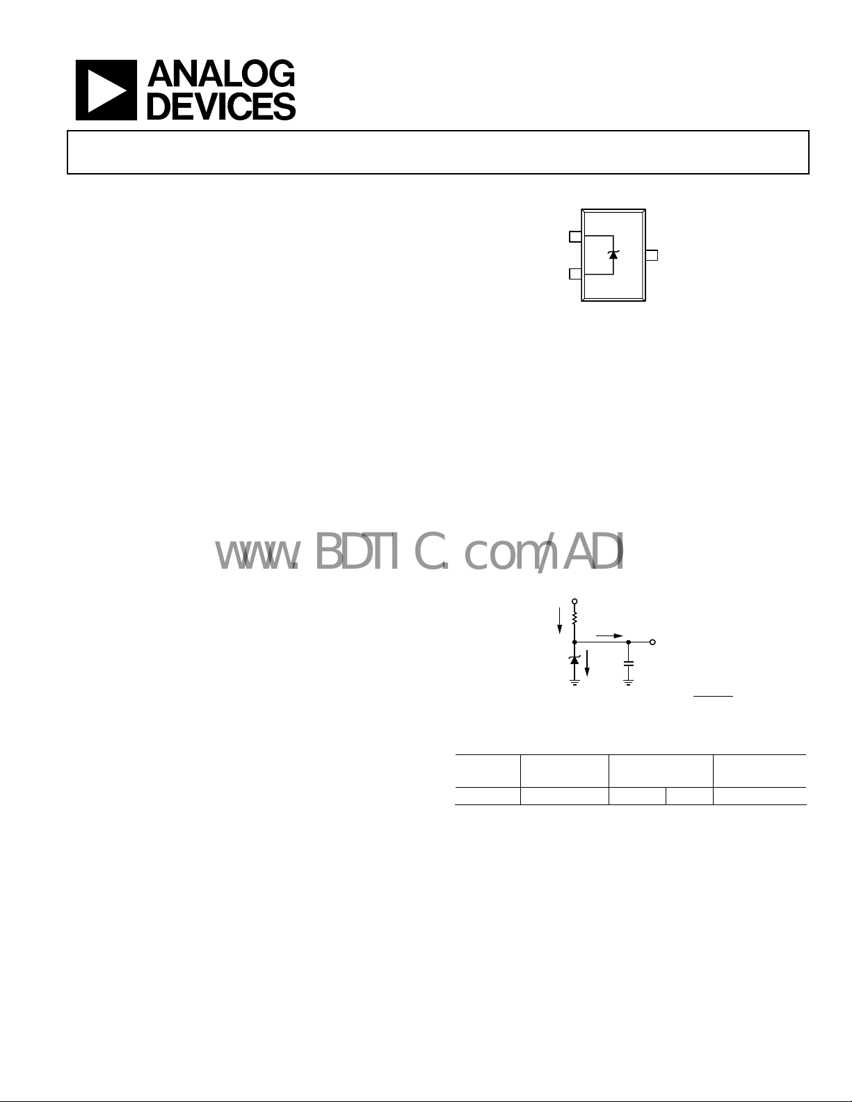
PIN CONFIGURATION
ADR510
V+
1
3
TRIM/NC
2
V–
TOP VIEW
(Not to Scale)
NC = NO CONNECT
Figure 1. 3-Lead SOT-23-3
03270-001
GENERAL DESCRIPTION
Designed for space critical applications, the ADR510 is a low
voltage (1.000 V), precision shunt-mode voltage reference in an
ultracompact (3 mm × 3 mm) SOT-23-3 package. The ADR510
features low temperature drift (70 ppm/°C), high accuracy
(±0.35%), and ultralow noise (4 μV p-p) performance.
The ADR510 advanced design eliminates the need for an external
pacitor, yet it is stable with any capacitive load. The minimum
ca
operating current increases from 100 μA to a maximum of 10 mA.
This low operating current and ease of use make the ADR510
ideally suited for handheld battery-powered applications.
A TRIM terminal is available on the ADR510 to provide
djustment of the output voltage over ±0.5% without affecting
a
the temperature coefficient of the device. This feature provides
users with the flexibility to trim out any system errors.
S
IL + I
ADR510
R
Q
BIAS
I
L
V
OUT
I
Figure 2. Typical Operating Circuit
C
Q
OUT
(OPTIONAL)
R
BIAS
= 1.0V
VS – V
=
IL + I
OUT
Q
3270-002
Table 1. ADR510
Part
Output
Vo
ltag e, V
Initial Accuracy
OUT
Temperature
Coefficient
ADR510A 1.000 V 3.5 mV 0.35% 70 ppm/°C
Rev. B
Information furnished by Analog Devices is believed to be accurate and reliable. However, no
responsibility is assumed by Anal og Devices for its use, nor for any infringements of patents or ot her
rights of third parties that may result from its use. Specifications subject to change without notice. No
license is granted by implication or otherwise under any patent or patent rights of Analog Devices.
Trademarks and registered trademarks are the property of their respective owners.
One Technology Way, P.O. Box 9106, Norwood, MA 02062-9106, U.S.A.
Tel: 781.329.4700 www.analog.com
Fax: 781.461.3113 ©2003–2007 Analog Devices, Inc. All rights reserved.
Page 2

ADR510
www.BDTIC.com/ADI
TABLE OF CONTENTS
Features.............................................................................................. 1
Applications....................................................................................... 1
Pin Configuration............................................................................. 1
General Description ......................................................................... 1
Revision History ............................................................................... 2
Specifications..................................................................................... 3
Electrical Characteristics ............................................................. 3
Absolute Maximum Ratings............................................................ 4
Thermal Resistance ...................................................................... 4
ESD Caution.................................................................................. 4
Typical Performance Characteristics ............................................. 5
REVISION HISTORY
9/07—Rev. A to Rev. B
Changes to Adjustable Precision Voltage Source Section ........... 8
Changes to Figure 11........................................................................ 8
Changes to Figure 12........................................................................ 8
4/07—Rev. 0 to Rev. A
Changes to Table 1............................................................................ 1
C
hanges to Table 3 and Table 4....................................................... 4
Changes to Figure 4, Figure 5, Figure 6, and Figure 7................. 5
Changes to Thermal Hysteresis Section ........................................ 7
Changes to Figure 11........................................................................ 8
Changes to Figure 14 and Equation 5............................................ 9
Changes to Ordering Guide.......................................................... 10
8/03—Revision 0: Initial Version
Parameter Definitions.......................................................................7
Temperature Coefficient...............................................................7
Thermal Hysteresis .......................................................................7
Applications Information.................................................................8
Adjustable Precision Voltage Source...........................................8
Output Voltage Trim.....................................................................8
Using the ADR510 with Precision Data Converters ................8
Precise Negative Voltage Reference ............................................9
Outline Dimensions....................................................................... 10
Ordering Guide .......................................................................... 10
Rev. B | Page 2 of 12
Page 3

ADR510
www.BDTIC.com/ADI
SPECIFICATIONS
ELECTRICAL CHARACTERISTICS
IIN = 100 μA to 10 mA @ TA = 25°C, unless otherwise noted.
Table 2.
Parameter Symbol Conditions Min Typ Max Unit
Output Voltage1 V
Initial Accuracy V
V
Temperature Coefficient, A Grade TCV
−40°C < TA < +85°C 85 ppm/°C
Output Voltage Change vs. IIN ∆VR IIN = 0.1 mA to 10 mA 3 mV
Dynamic Output Impedance (∆VR/∆IR) IIN = 1 mA ± 100 μA 0.3 Ω
Minimum Operating Current IIN 0°C < TA < 70°C 100 μA
Voltage Noise eN p-p f = 0.1 Hz to 10 Hz 4 μV p-p
Turn-On Settling Time2 tR To within 0.1% of output 10 μs
Output Voltage Hysteresis V
1
The forward diode voltage characteristic at −1 mA is typically 0.65 V.
2
Measured without a load capacitor.
0.9965 1.0 1.0035 V
OUT
−3.5 +3.5 mV
OUTERR
−0.35 +0.35 %
OUTERR%
0°C < TA < 70°C 70 ppm/°C
OUT
50 ppm
OUT_HYS
Rev. B | Page 3 of 12
Page 4
ADR510
www.BDTIC.com/ADI
ABSOLUTE MAXIMUM RATINGS
Table 3.
Parameter Rating
Reverse Current 25 mA
Forward Current 20 mA
Storage Temperature Range −65°C to +150°C
Operating Temperature Range −40°C to +85°C
Junction Temperature Range −65°C to +150°C
Lead Temperature (Soldering, 60 sec) 300°C
THERMAL RESISTANCE
θJA is specified for the worst-case conditions, that is, a device
soldered in a circuit board for surface-mount packages. Package
power dissipation = (T
Table 4. Thermal Resistance
Package Type θJA θ
3-Lead SOT-23-3 (RT-3) 230 146 °C/W
− TA)/θJA.
JMAX
Unit
JC
Stresses above those listed under Absolute Maximum Ratings
may cause permanent damage to the device. This is a stress
rating only; functional operation of the device at these or any
other conditions above those indicated in the operational
section of this specification is not implied. Exposure to absolute
maximum rating conditions for extended periods may affect
device reliability.
ESD CAUTION
Rev. B | Page 4 of 12
Page 5

ADR510
www.BDTIC.com/ADI
TYPICAL PERFORMANCE CHARACTERISTICS
1.002
1.001
VIN = 5V/DIV
1.000
(V)
OUT
V
0.999
= 500mV/DIV
V
0.998
OUT
0.997
07
Figure 3. Typical V
TEMPERATURE (° C)
vs. Temperature
OUT
TIME (400n s/DIV)
VIN = 5V/DIV
V
= 500mV/DIV
OUT
Figure 4. Turn-On Time
VIN = 5V/DIV
605040302010
0
03270-003
3270-004
Figure 7. Turn-Off Time with 1 μF Input Capacitor
TIME (400n s/DIV)
Figure 6. Turn-Off Time
VIN = 5V/DIV
= 500mV/DIV
V
OUT
TIME (1ms/DIV)
ΔIIN = 100µA
3270-006
3270-007
V
= 500mV/DIV
OUT
TIME (400µ s/DIV)
3270-005
Figure 5. Turn-On Time with 1 μF Input Capacitor
Rev. B | Page 5 of 12
= 50mV/DIV
V
OUT
TIME (2µs/DIV)
Figure 8. Output Response to 100 μA Input Current Change
3270-008
Page 6

ADR510
www.BDTIC.com/ADI
ΔIIN = 100µA
2µV/DIV
= 50mV/DIV
V
OUT
TIME (2µs/DIV)
Figure 9. Output Response to 100 μA Input Current Change
with
1 μF Capacitor
3270-009
TIME (400ms/ DIV)
Figure 10. 1 Hz to 10 Hz Noise
3270-010
Rev. B | Page 6 of 12
Page 7

ADR510
=
www.BDTIC.com/ADI
PARAMETER DEFINITIONS
TEMPERATURE COEFFICIENT
This is the change of output voltage with respect to the
operating temperature changes, normalized by the output
voltage at 25°C. This parameter is expressed in parts per
million/degrees Celsius (ppm/°C) and can be determined with
the following equation:
C][ppm/ ×
TCV
OUT
=°
OUT
where:
V
(25°C) is the output voltage at 25°C.
OUT
) is the output voltage at Temperature 1.
V
OUT(T1
V
) is the output voltage at Temperature 2.
OUT(T2
−
)()(
T1VT2V
OUTOUT
−×°
T1T2C25V
)()(
6
(1)
10
THERMAL HYSTERESIS
Thermal hysteresis is the change of output voltage after the
device is cycled through the temperature from 25°C to 0°C to
85°C and back to 25°C.
VC25VV
)( −°
[ppm] ×
V
_
HYSOUT
=
OUT
where:
V
(25°C) is the output voltage at 25°C.
OUT
is the output voltage at 25°C after temperature cycle at
V
OUT_TC
+25°C to −40°C to +85°C and back to +25°C.
TCOUTOUTHYSOUT
__
)(
−°
VC25V
_
TCOUTOUT
6
10
)(
°
C25V
(2)
Rev. B | Page 7 of 12
Page 8

ADR510
V
A
V
www.BDTIC.com/ADI
APPLICATIONS INFORMATION
The ADR510 is a 1.0 V precision shunt voltage reference
designed to operate without an external output capacitor
between the positive terminal and the negative terminal for
stability. An external capacitor can be used for additional
filtering of the supply.
As with all shunt voltage references, an external bias resistor
) is required between the supply voltage and the ADR510
(R
BIAS
(see
Figure 2). R
through the load (I
supply voltage can vary, thus R
sets the current that is required to pass
BIAS
) and the ADR510 (IQ). The load and the
L
is chosen based on the
BIAS
following conditions:
• R
must be small enough to supply the minimum IQ
BIAS
current to the ADR510 even when the supply voltage is at
minimum value and the load current is at maximum value.
• R
also needs to be large enough so that IQ does not
BIAS
exceed 10 mA when the supply voltage is at its maximum
value and the load current is at its minimum value.
Given these conditions, R
voltage (V
), the load and operating current (IL and IQ) of the
S
is determined by the supply
BIAS
ADR510, and the ADR510 output voltage.
VV
−
S
R
=
BIAS
OUT
II
+
L
Q
(3)
ADJUSTABLE PRECISION VOLTAGE SOURCE
The ADR510, combined with a precision low input bias op amp
such as the AD860x, can be used to output a precise adjustable
voltage. Figure 11 illustrates implementation of this application
usin
g the ADR510.
Output of the op amp, V
the circuit, which is completely dependent on the R2 and R1
resistors.
R2
V
OUT
+= 1
R1
An additional capacitor in parallel with R2 can be added to
ilter out high frequency noise. The value of C2 is dependent on
f
the value of R2.
CC
, is determined by the gain of
OUT
(4)
OUTPUT VOLTAGE TRIM
Using a mechanical or digital potentiometer, the output voltage
of the ADR510 can be trimmed ±0.5%. The circuit in Figure 12
llustrates how the output voltage can be trimmed using a
i
10 kΩ potentiometer. Note that trimming using other resistor
values may not produce an accurate output from the ADR510.
CC
R
BIAS
V
OUT
03270-012
ADR510
1
3
R1
470kΩ
2
Figure 12. Output Voltage Trim
POT
10kΩ
USING THE ADR510 WITH PRECISION DATA CONVERTERS
The compact ADR510 and its low minimum operating current
requirement make it ideal for use in battery-powered portable
instruments, such as the AD7533 CMOS multiplying DAC, that
us
e precision data converters.
Figure 13 shows the ADR510 serving as an external reference to
th
e
AD7533, a CMOS multiplying DAC. Such a DAC requires a
gative voltage input in order to provide a positive output
ne
range. In this application, the ADR510 is supplying a −1.0 V
reference to the REF input of the
MSB
V
DD
G
N
0
1
1
32 1 15
ADR510
Figure 13. ADR510 as a Reference for a 10-Bit CMOS DAC (AD7533)
+
–
R2
–V
DD
AD7533.
9
AD7533
LSB
+
V
OUT
–
= 0V TO 1.0V
3270-013
R
BIAS
1.0V
V
AD860x
DR510
R1
Figure 11. Adjustable Precision Voltage Source
R2
C2
(OPTIO NAL)
= (1 + R2/R1)
OUT
03270-011
Rev. B | Page 8 of 12
Page 9

ADR510
I
www.BDTIC.com/ADI
PRECISE NEGATIVE VOLTAGE REFERENCE
The ADR510 is suitable for use in applications where a precise
negative voltage reference is desired, including the application
detailed in Figure 13.
Figure 14 shows the ADR510 configured to provide an output
f −1.0 V.
o
ADR510
Figure 14. Precise −1.0 V Reference Configuration
+
–
–1.0V
I
R1
–V
DD
03270-014
Because the ADR510 characteristics resemble those of a Zener
diode, the cathode shown in
espect to the anode (V+ with respect to V− on the ADR510
r
Figure 14 is 1.0 V higher with
package). Because the cathode of the ADR510 is tied to ground,
the anode must be −1.0 V.
R1 in Figure 14 should be chosen so that 100 μA to 10 mA is
p
rovided to properly bias the ADR510.
V
)(1 −−−
R1
=
DD
(5)
The R1 resistor should be chosen so that power dissipation is at
nimum. An ideal resistor value can be determined through
a mi
manipulation of Equation 5.
Rev. B | Page 9 of 12
Page 10

ADR510
www.BDTIC.com/ADI
OUTLINE DIMENSIONS
3.04
2.90
1.40
1.30
1.20
PIN 1
0.10
0.01
Figure 15. 3-Lead Small Outline Transistor Package [SOT-23-3]
2.80
3
1
1.90 BSC
SEATING
PLANE
COMPLIANT TO JEDEC STANDARDS TO-236-AB
2
0.95 BSC
2.64
2.10
0.50
0.30
1.12
0.89
0.60
0.50
0.40
(RT-3)
Dimensions shown in millimeters
0.20
0.08
ORDERING GUIDE
Output
Model
(V
OUT
Initial Accuracy
)
ADR510ART-REEL7 1.0 V 3.5 mV 0.35% 70 ppm/°C −40°C to +85°C 3-Lead SOT-23-3 RT-3 3,000 RAA
ADR510ART-R2 1.0 V 3.5 mV 0.35% 70 ppm/°C −40°C to +85°C 3-Lead SOT-23-3 RT-3 250 RAA
ADR510ARTZ-REEL71 1.0 V 3.5 mV 0.35% 70 ppm/°C −40°C to +85°C 3-Lead SOT-23-3 RT-3 3,000 RAA#
ADR510ARTZ-R21 1.0 V 3.5 mV 0.35% 70 ppm/°C −40°C to +85°C 3-Lead SOT-23-3 RT-3 250 RAA#
1
Z = RoHS Compliant Part. # denotes lead free, may be top or bottom marked.
Voltage
Temperature
Coefficient
Temperature
Range
Package
Description
Package
Option
Ordering
Quantity
Branding
Rev. B | Page 10 of 12
Page 11

ADR510
www.BDTIC.com/ADI
NOTES
Rev. B | Page 11 of 12
Page 12

ADR510
www.BDTIC.com/ADI
NOTES
©2003–2007 Analog Devices, Inc. All rights reserved. Trademarks and
registered trademarks are the property of their respective owners.
D03270-0-9/07(B)
Rev. B | Page 12 of 12
 Loading...