

Page 1
G
查询ADR364供应商
Low Power, Low Noise Voltage References
FEATURES
Compact TSOT-23-5 packages
Low temperature coefficient
B grade: 9 ppm/°C
A grade: 25 ppm/°C
Initial accuracy
B grade: ±3 mV maximum
A grade: ±6 mV maximum
Ultralow output noise: 6.8 µV p-p (0.1 Hz to 10 Hz)
Low dropout: 300 mV
Low supply current: 190 µA, Maximum
No external capacitor required
Output current: +5 mA/−1 mA
Wide temperature range: −40°C to +125°C
APPLICATIONS
Battery-powered instrumentations
Portable medical instrumentations
Data acquisition systems
Industrial process controls
Automotive
GENERAL DESCRIPTION
ADR360/ADR361/ADR363/ADR364/ADR365/ADR366
with Sink/Source Capability
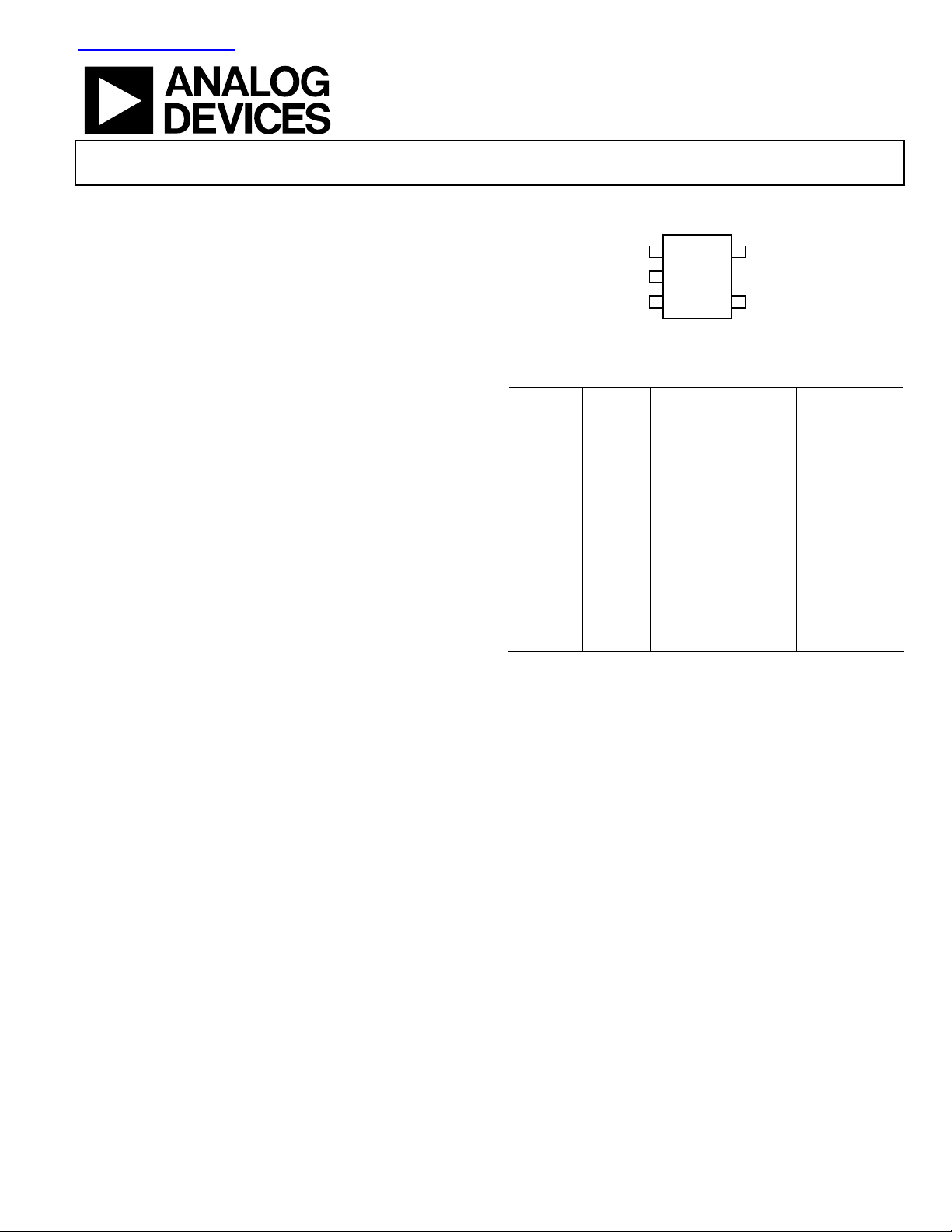
PIN CONFIGURATION
NC
1
ADR36x
TOP VIEW
ND
2
(Not to Scale)
3
V
IN
NC = NO CONNECT
Figure 1. 5-Lead TSOT (UJ Suffix)
Table 1.
Temperature
Model V
OUT
1
(V)
Coefficient (ppm/°C) Accuracy (mV)
ADR360B 2.048 9 ±3
ADR360A 2.048 25 ±6
ADR361B 2.5 9 ±3
ADR361A 2.5 25 ±6
ADR363B 3.0 9 ±3
ADR363A 3.0 25 ±6
ADR364B 4.096 9 ±4
ADR364A 4.096 25 ±8
ADR365B 5.0 9 ±4
ADR365A 5.0 25 ±8
ADR366B 3.3 9 ±4
ADR366A 3.3 25 ±8
1
Contact Analog Devices, Inc. for other voltage options.
TRIM
5
4
V
OUT
05467-001
The ADR360/ADR361/ADR363/ADR364/ADR365/ADR366
are precision 2.048 V, 2.5 V, 3.0 V, 4.096 V, 5.0 V, and 3.3 V band
gap voltage references that feature low power, high precision in
a tiny footprint. Using ADI’s patented temperature drift
curvature correction techniques, the ADR36x references achieve
a low temperature drift of 9 ppm/°C in the TSOT package.
The ADR36x family of micropower, low dropout voltage
references provides a stable output voltage from a minimum
supply of 300 mV above the output. Their advanced design
eliminates the need for external capacitors, which further
reduces board space and system cost. The combination of low
power operation, small size, and ease of use makes the ADR36x
precision voltage references ideally suited for battery-operated
applications.
Rev. 0
Information furnished by Analog Devices is believed to be accurate and reliable.
However, no responsibility is assumed by Analog Devices for its use, nor for any
infringements of patents or other rights of third parties that may result from its use.
Specifications subject to change without notice. No license is granted by implication
or otherwise under any patent or patent rights of Analog Devices. Trademarks and
registered trademarks are the property of their respective owners.
One Technology Way, P.O. Box 9106, Norwood, MA 02062-9106, U.S.A.
Tel: 781.329.4700
Fax: 781.461.3113 © 2005 Analog Devices, Inc. All rights reserved.
www.analog.com
Page 2

ADR360/ADR361/ADR363/ADR364/ADR365/ADR366
TABLE OF CONTENTS
ADR360—Specifications ................................................................. 3
ESD Caution...................................................................................9
ADR361—Specifications ................................................................. 4
ADR363—Specifications ................................................................. 5
ADR364—Specifications ................................................................. 6
ADR365—Specifications ................................................................. 7
ADR366—Specifications ................................................................. 8
Absolute Maximum Ratings............................................................ 9
Thermal Resistance ...................................................................... 9
REVISION HISTORY
4/05—Revision 0: Initial Version
Te r m in o l o g y .................................................................................... 10
Typical Perfor m a n c e Character i s t ics ........................................... 11
Theory of Operation...................................................................... 16
Applications..................................................................................... 17
Basic Voltage Reference Connection ....................................... 17
Outline Dimensions....................................................................... 19
Ordering Guide .......................................................................... 19
Rev. 0 | Page 2 of 20
Page 3

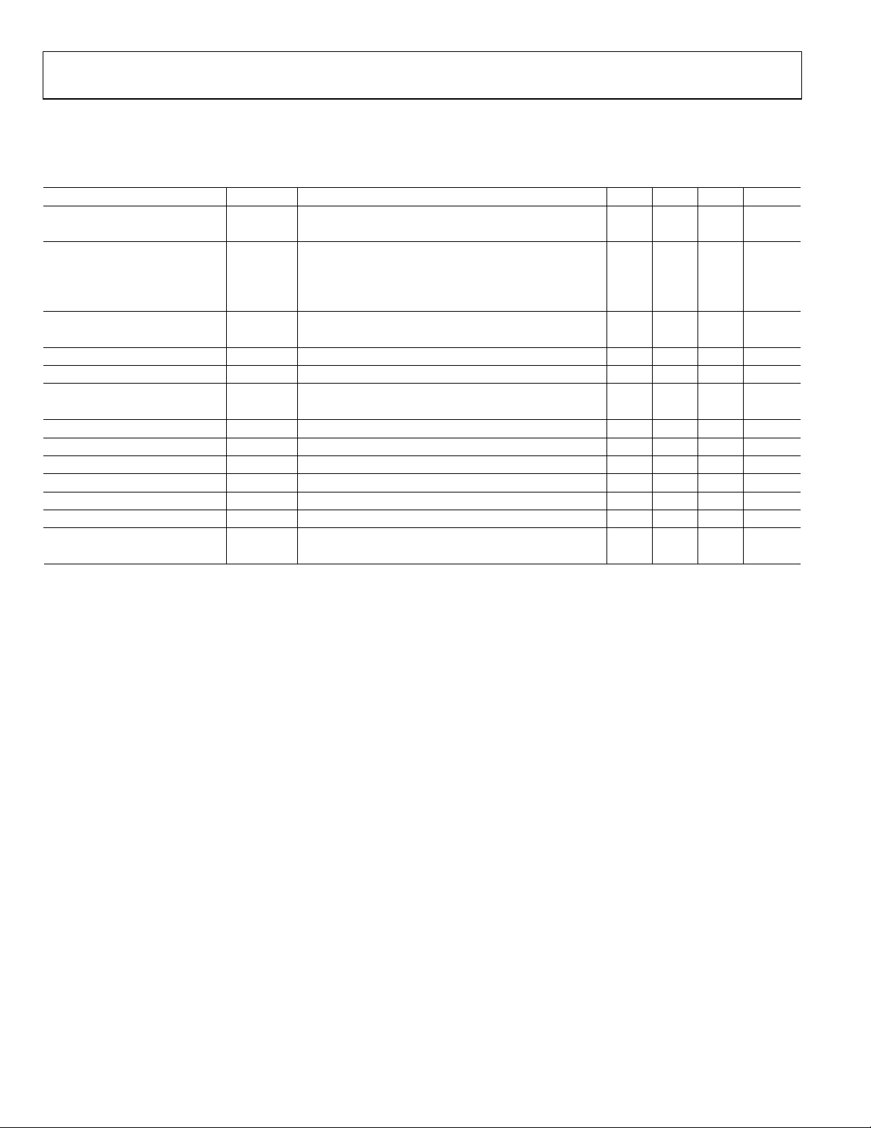
ADR360/ADR361/ADR363/ADR364/ADR365/ADR366
ADR360—SPECIFICATIONS
Electrical Characteristics (VIN = 2.35 V to 15 V, TA = 25°C, unless otherwise noted.)
Table 2.
Parameter Symbol Conditions Min Typ Max Unit
OUTPUT VOLTAGE V
V
INITIAL ACCURACY V
V
V
V
O
O
OERR
OERR
OERR
OERR
O
SUPPLY VOLTAGE HEADROOM VIN − V
LINE REGULATION ∆VO/∆V
QUIESCENT CURRENT I
VOLTAGE NOISE e
TURN-ON SETTLING TIME t
LONG-TERM STABILITY
1
OUTPUT VOLTAGE HYSTERESIS ∆V
∆V
IN
N p-p
R
O
O_HYS
RIPPLE REJECTION RATIO RRR fIN = 60 kHz 70 dB
SC
1
The long-term stability specification is noncumulative. The drift subsequent 1,000 hour periods are significantly lower than in the first 1,000 hour period.
A Grade 2.042 2.048 2.054 V
B Grade 2.045 2.048 2.051 V
A Grade 6 mV
A Grade 0.29 %
B Grade 3 mV
B Grade 0.15 %
A Grade, −40°C < TA < +125°C 25 ppm/°C TEMPERATURE COEFFICIENT TCV
B Grade, −40°C < TA < +125°C 9 ppm/°C
300 mV
O
VIN = 2.45 V to 15 V, −40°C < TA < +125°C 0.105 mV/V
IN
I
= 0 mA to 5 mA, −40°C < TA < +125°C, VIN = 3 V 0.37 mV/mA LOAD REGULATION ∆VO/∆I
LOAD
LOAD
I
= −1 mA to 0 mA, −40°C < TA < +125°C, VIN = 3 V 0.82 mV/mA
LOAD
−40°C < TA < +125°C 150 190 µA
0.1 Hz to 10 Hz 6.8 µV p-p
25 µs
1, 000 Hours 50 ppm
100 ppm
VIN = 5 V 25 mA SHORT CIRCUIT TO GND I
VIN = 15 V 30 mA
Rev. 0 | Page 3 of 20
Page 4
ADR360/ADR361/ADR363/ADR364/ADR365/ADR366
ADR361—SPECIFICATIONS
Electrical Characteristics (VIN = 2.8 V to 15 V, TA = 25°C, unless otherwise noted.)
Table 3.
Parameter Symbol Conditions Min Typ Max Unit
OUTPUT VOLTAGE V
V
INITIAL ACCURACY V
V
V
V
O
O
OERR
OERR
OERR
OERR
O
SUPPLY VOLTAGE HEADROOM VIN − V
LINE REGULATION ∆VO/∆V
QUIESCENT CURRENT I
VOLTAGE NOISE e
TURN-ON SETTLING TIME t
LONG-TERM STABILITY
1
OUTPUT VOLTAGE HYSTERESIS ∆V
IN
∆V
N p-p
R
O
O_HYS
RIPPLE REJECTION RATIO RRR fIN = 60 kHz 70 dB
SC
1
The long-term stability specification is noncumulative. The drift subsequent 1,000 hour periods are significantly lower than in the first 1,000 hour period.
A Grade 2.494 2.500 2.506 V
B Grade 2.497 2.500 2.503 V
A Grade 6 mV
A Grade 0.24 %
B Grade 3 mV
B Grade 0.12 %
A Grade, −40°C < TA < +125°C 25 ppm/°C TEMPERATURE COEFFICIENT TCV
B Grade, −40°C < TA < +125°C 9 ppm/°C
300 mV
O
VIN = 2.8 V to 15 V, −40°C < TA < +125°C 0.125 mV/V
IN
I
= 0 mA to 5 mA, −40°C < TA < +125°C, VIN = 3.5 V 0.45 mV/mA LOAD REGULATION ∆VO/∆I
LOAD
LOAD
I
= −1 mA to 0 mA, −40°C < TA < +125°C, VIN = 3.5 V 1 mV/mA
LOAD
−40°C < TA < +125°C 150 190 µA
0.1 Hz to 10 Hz 8.25 µV p-p
25 µs
1, 000 Hours 50 ppm
100 ppm
VIN = 5 V 25 mA SHORT CIRCUIT TO GND I
VIN = 15 V 30 mA
Rev. 0 | Page 4 of 20
Page 5
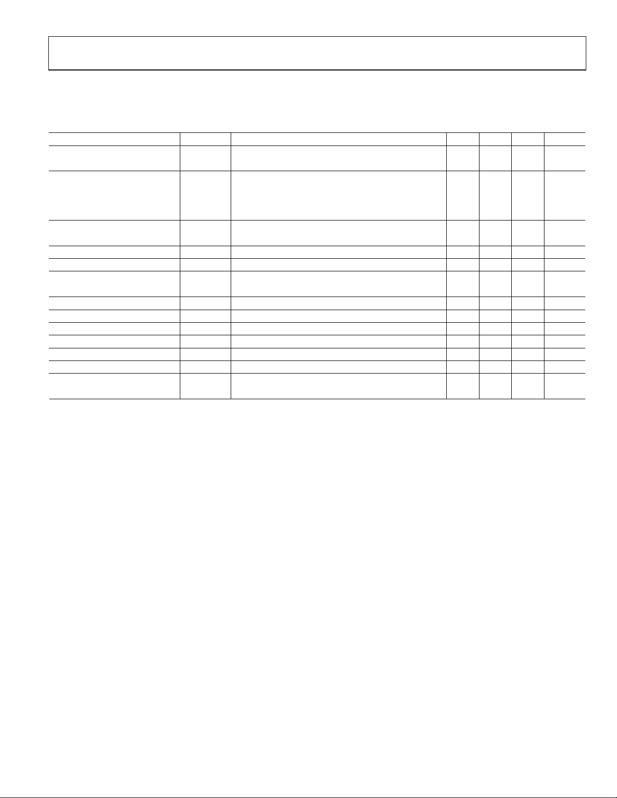
ADR360/ADR361/ADR363/ADR364/ADR365/ADR366
ADR363—SPECIFICATIONS
Electrical Characteristics (VIN = 3.3 V to 15 V, TA = 25°C, unless otherwise noted.)
Table 4.
Parameter Symbol Conditions Min Typ Max Unit
OUTPUT VOLTAGE V
V
INITIAL ACCURACY V
V
V
V
O
O
OERR
OERR
OERR
OERR
O
SUPPLY VOLTAGE HEADROOM VIN − V
LINE REGULATION ∆VO/∆V
QUIESCENT CURRENT I
VOLTAGE NOISE e
TURN-ON SETTLING TIME t
LONG-TERM STABILITY
1
OUTPUT VOLTAGE HYSTERESIS ∆V
∆V
IN
N p-p
R
O
O_HYS
RIPPLE REJECTION RATIO RRR fIN = 60 kHz 70 dB
SC
1
The long-term stability specification is noncumulative. The drift subsequent 1,000 hour periods are significantly lower than in the first 1,000 hour period.
A Grade 2.994 3.000 3.006 V
B Grade 2.997 3.000 3.003 V
A Grade 6 mV
A Grade 0.2 %
B Grade 3 mV
B Grade 0.1 %
A Grade, −40°C < TA < +125°C 25 ppm/°C TEMPERATURE COEFFICIENT TCV
B Grade, −40°C < TA < +125°C 9 ppm/°C
300 mV
O
VIN = 3.3 V to 15 V, −40°C < TA < +125°C 0.15 mV/V
IN
I
= 0 mA to 5 mA, −40°C < TA < +125°C, VIN = 4 V 0.54 mV/mA LOAD REGULATION ∆VO/∆I
LOAD
LOAD
I
= −1 mA to 0 mA, −40°C < TA < +125°C, VIN = 4 V 1.2 mV/mA
LOAD
−40°C < TA < +125°C 150 190 µA
0.1 Hz to 10 Hz 8.7 µV p-p
25 µs
1, 000 Hours 50 ppm
100 ppm
VIN = 5 V 25 mA SHORT CIRCUIT TO GND I
VIN = 15 V 30 mA
Rev. 0 | Page 5 of 20
Page 6

ADR360/ADR361/ADR363/ADR364/ADR365/ADR366
ADR364—SPECIFICATIONS
Electrical Characteristics (VIN = 4.4 V to 15 V, TA = 25°C, unless otherwise noted.)
Table 5.
Parameter Symbol Conditions Min Typ Max Unit
OUTPUT VOLTAGE V
V
INITIAL ACCURACY V
V
V
V
O
O
OERR
OERR
OERR
OERR
O
SUPPLY VOLTAGE HEADROOM VIN − V
LINE REGULATION ∆VO/∆V
QUIESCENT CURRENT I
VOLTAGE NOISE e
TURN-ON SETTLING TIME t
LONG-TERM STABILITY
1
OUTPUT VOLTAGE HYSTERESIS ∆V
IN
∆V
N p-p
R
O
O_HYS
RIPPLE REJECTION RATIO RRR fIN = 60 kHz 70 dB
SC
1
The long-term stability specification is noncumulative. The drift subsequent 1,000 hour periods are significantly lower than in the first 1,000 hour period.
A Grade 4.088 4.096 4.104 V
B Grade 4.092 4.096 4.100 V
A Grade 8 mV
A Grade 0.2 %
B Grade 4 mV
B Grade 0.1 %
A Grade, −40°C < TA < +125°C 25 ppm/°C TEMPERATURE COEFFICIENT TCV
B Grade, −40°C < TA < +125°C 9 ppm/°C
300 mV
O
VIN = 4.4 V to 15 V, −40°C < TA < +125°C 0.205 mV/V
IN
I
= 0 mA to 5 mA, −40°C < TA < +125°C, VIN = 5 V 0.735 mV/mA LOAD REGULATION ∆VO/∆I
LOAD
LOAD
I
= −1 mA to 0 mA, −40°C < TA < +125°C, VIN = 5 V 1.75 mV/mA
LOAD
−40°C < TA < +125°C 150 190 µA
0.1 Hz to 10 Hz 11 µV p-p
25 µs
1, 000 Hours 50 ppm
100 ppm
VIN = 5 V 25 mA SHORT CIRCUIT TO GND I
VIN = 15 V 30 mA
Rev. 0 | Page 6 of 20
Page 7

ADR360/ADR361/ADR363/ADR364/ADR365/ADR366
ADR365—SPECIFICATIONS
Electrical Characteristics (VIN = 5.3 V to 15 V, TA = 25°C, unless otherwise noted.)
Table 6.
Parameter Symbol Conditions Min Typ Max Unit
OUTPUT VOLTAGE V
V
INITIAL ACCURACY V
V
V
V
O
O
OERR
OERR
OERR
OERR
O
SUPPLY VOLTAGE HEADROOM VIN − V
LINE REGULATION ∆VO/∆V
QUIESCENT CURRENT I
VOLTAGE NOISE e
TURN-ON SETTLING TIME t
LONG-TERM STABILITY
1
OUTPUT VOLTAGE HYSTERESIS ∆V
∆V
IN
N p-p
R
O
O_HYS
RIPPLE REJECTION RATIO RRR fIN = 60 kHz 70 dB
SC
1
The long-term stability specification is noncumulative. The drift subsequent 1,000 hour periods are significantly lower than in the first 1,000 hour period.
A Grade 4.992 5.000 5.008 V
B Grade 4.996 5.000 5.004 V
A Grade 8 mV
A Grade 0.16 %
B Grade 4 mV
B Grade 0.08 %
A Grade, −40°C < TA < +125°C 25 ppm/°C TEMPERATURE COEFFICIENT TCV
B Grade, −40°C < TA < +125°C 9 ppm/°C
300 mV
O
VIN = 5.3 V to 15 V, −40°C < TA < +125°C 0.25 mV/V
IN
I
= 0 mA to 5 mA, −40°C < TA < +125°C, VIN = 6V 0.9 mV/mA LOAD REGULATION ∆VO/∆I
LOAD
LOAD
I
= −1 mA to 0 mA, −40°C < TA < +125°C, VIN = 6 V 2 mV/mA
LOAD
−40°C < TA < +125°C 150 190 µA
0.1 Hz to 10 Hz 12.8 µV p-p
20 µs
1, 000 Hours 50 ppm
100 ppm
VIN = 5 V 25 mA SHORT CIRCUIT TO GND I
VIN = 15 V 30 mA
Rev. 0 | Page 7 of 20
Page 8

ADR360/ADR361/ADR363/ADR364/ADR365/ADR366
ADR366—SPECIFICATIONS
Electrical Characteristics (VIN = 3.6 V to 15 V, TA = 25°C, unless otherwise noted.)
Table 7.
Parameter Symbol Conditions Min Typ Max Unit
OUTPUT VOLTAGE V
V
INITIAL ACCURACY V
V
V
V
O
O
OERR
OERR
OERR
OERR
O
SUPPLY VOLTAGE HEADROOM VIN − V
LINE REGULATION ∆VO/∆V
QUIESCENT CURRENT I
VOLTAGE NOISE e
TURN-ON SETTLING TIME t
LONG-TERM STABILITY
1
OUTPUT VOLTAGE HYSTERESIS ∆V
IN
R
∆V
N p-p
O
O_HYS
RIPPLE REJECTION RATIO RRR fIN = 60 kHz 70 dB
SC
1
The long-term stability specification is noncumulative. The drift subsequent 1,000 hour periods are significantly lower than in the first 1,000 hour period.
A Grade 3.292 3.300 3.308 V
B Grade 3.296 3.300 3.304 V
A Grade 8 mV
A Grade 0.25 %
B Grade 4 mV
B Grade 0.125 %
A Grade, −40°C < TA < +125°C 25 ppm/°C TEMPERATURE COEFFICIENT TCV
B Grade, −40°C < TA < +125°C 9 ppm/°C
300 mV
O
VIN = 3.6 V to 15 V, −40°C < TA < +125°C 0.165 mV/V
IN
I
= 0 mA to 5 mA, −40°C < TA < +125°C, VIN = 4.2 V 0.6 mV/mA LOAD REGULATION ∆VO/∆I
LOAD
LOAD
I
= −1 mA to 0 mA, −40°C < TA < +125°C, VIN = 4.2 V 1.35 mV/mA
LOAD
−40°C < TA < +125°C 150 190 µA
0.1 Hz to 10 Hz 9.3 µV p-p
25 µs
1, 000 Hours 50 ppm
100 ppm
VIN = 5 V 25 mA SHORT CIRCUIT TO GND I
VIN = 15 V 30 mA
Rev. 0 | Page 8 of 20
Page 9

ADR360/ADR361/ADR363/ADR364/ADR365/ADR366
ABSOLUTE MAXIMUM RATINGS
@ 25°C, unless otherwise noted.
Table 8.
Parameter Rating
Supply Voltage 18 V
Output Short-Circuit Duration to GND
V
< 15 V
IN
V
> 15 V
IN
Storage Temperature Range −65°C to +125°C
Operating Temperature Range –40°C to +125°C
Junction Temperature Range –65°C to +125°C
Lead Temperature Range (Soldering, 60 sec) 300°C
Indefinite
10 sec
Stresses above those listed under Absolute Maximum Ratings
may cause permanent damage to the device. This is a stress
rating only; functional operation of the device at these or any
other conditions above those indicated in the operational
section of this specification is not implied. Exposure to absolute
maximum rating conditions for extended periods may affect
device reliability.
THERMAL RESISTANCE
θJA is specified for the worst-case conditions, that is, θJA is
specified for device soldered in circuit board for surface-mount
packages.
Table 9. Thermal Resistance
Package Type θ
TSOT-23-5 (UJ-5) 230 146 °C/W
JA
θ
JC
Unit
ESD CAUTION
ESD (electrostatic discharge) sensitive device. Electrostatic charges as high as 4000 V readily accumulate on the
human body and test equipment and can discharge without detection. Although this product features
proprietary ESD protection circuitry, permanent damage may occur on devices subjected to high energy
electrostatic discharges. Therefore, proper ESD precautions are recommended to avoid performance
degradation or loss of functionality.
Rev. 0 | Page 9 of 20
Page 10

ADR360/ADR361/ADR363/ADR364/ADR365/ADR366
()(
)
(
TERMINOLOGY
Temperature Coefficient
Thermal Hysteresis
The change of output voltage with respect to operating
temperature changes normalized by the output voltage at 25°C.
This parameter is expressed in ppm/°C and can be determined
by
[]
Cppm/ ×
TCV
O
=°
OO
()
O
25
×°
()
T–VTV
12
–TTCV
6
10
12
where:
V
(25°C) = VO at 25°C.
O
V
(T1) = VO at Temperature 1.
O
V
(T2) = VO at Temperature 2.
O
Line Regulation
The change in output voltage due to a specified change in input
voltage. This parameter accounts for the effects of self-heating.
Line regulation is expressed in either percent per volt, partsper-million per volt, or microvolts per volt change in input
voltage.
Load Regulation
The change in output voltage due to a specified change in load
current. This parameter accounts for the effects of self-heating.
Load regulation is expressed in either microvolts per
milliampere, parts-per-million per milliampere, or ohms of dc
output resistance.
Long-Term Stability
Typical shift of output voltage at 25°C on a sample of parts
subjected to a test of 1,000 hours at 25°C.
∆
V
= VO(t0) – VO(t1)
O
⎛
[]
O
⎜
ppmΔV
⎜
⎝
()
()
tV
O
()
OO
0
t–VtV
⎞
6
10
⎟
10
×=
⎟
⎠
The change of output voltage after the device is cycled through
temperature from +25°C to –40°C to +125°C and back to
+25°C. This is a typical value from a sample of parts put
through such a cycle.
V
= VO(25°C) – V
O_HYS
[]
ppmV
O_HYS
=
O_TC
°
O
()
25
O
)
–25
VCV
O_TC
°
CV
6
×
10
where:
V
(25°C) = VO at 25°C.
O
V
= VO at 25°C after temperature cycle at +25°C to –40°C to
O_TC
+125°C and back to +25°C.
NOTES
Input Capacitor
Input capacitors are not required on the ADR36x. There is no
limit for the value of the capacitor used on the input, but a 1 µF
to 10 µF capacitor on the input improves transient response in
applications where the supply suddenly changes. An additional
0.1 µF capacitor in parallel also helps reduce noise from the
supply.
Output Capacitor
The ADR36x does not require output capacitors for stability
under any load condition. An output capacitor, typically 0.1 µF,
filters out any low level noise voltage and does not affect the
operation of the part. On the other hand, the load transient
response can improve with an additional 1 µF to 10 µF output
capacitor in parallel. A capacitor here acts as a source of stored
energy for a sudden increase in load current. The only
parameter that degrades by adding an output capacitor is the
turn-on time. The degradation depends on the size of the
capacitor chosen.
where:
V
(t0) = VO at 25°C at Time 0.
O
V
(t1) = VO at 25°C after 1,000 hours operation at 25°C.
O
Rev. 0 | Page 10 of 20
Page 11

ADR360/ADR361/ADR363/ADR364/ADR365/ADR366
TYPICAL PERFORMANCE CHARACTERISTICS
2.052
4.998
4.997
2.050
(V)
2.048
OUT
V
2.046
2.044
–20 0 20 40 60 80 100 120
–40
TEMPERATURE (°C)
Figure 2. ADR360 Output Voltage vs. Temperature
2.504
2.502
2.500
(V)
OUT
V
2.498
2.496
05467-002
4.996
4.995
(V)
4.994
OUT
V
4.993
4.992
4.991
4.990
–25–105 203550658095110
–40
TEMPERATURE (°C)
Figure 5. ADR365 Output Voltage vs. Temperature
0.165
0.155
0.145
IDD (mA)
0.135
0.125
+125°C
+25°C
–40°C
125
05467-005
2.494
–25–105 203550658095110
–40
TEMPERATURE (°C)
Figure 3. ADR361 Output Voltage vs. Temperature
3.003
3.002
3.001
3.000
(V)
OUT
V
2.999
2.998
2.997
2.996
–20 0 20 40 60 80 100 120
–40
TEMPERATURE (°C)
Figure 4. ADR363 Output Voltage vs. Temperature
125
05467-003
05467-004
0.115
2.8
4.1 5.3 6.6 7.8 9.1 10.3 11.6 12.8 14.1
SUPPLY VOLTAGE (V)
Figure 6. ADR361 Supply Current vs. Input Voltage
0.17
+125°C
0.16
+25°C
IDD (mA)
0.15
0.14
5.3
6.3 7.3 8.3 9.3 10.3 11.3 12.3 13.3 14.3
VIN (V)
Figure 7. ADR365 Supply Current vs. Input Voltage
05467-006
–40°C
05467-007
Rev. 0 | Page 11 of 20
Page 12

ADR360/ADR361/ADR363/ADR364/ADR365/ADR366
0.18
0.16
0.14
0.12
0.10
0.08
0.06
0.04
LOAD REGULATION (mV/mA)
0.02
0.14
VIN = 9V
VIN = 3.5V
0
–40 125
–25–105 203550658095110
TEMPERATURE (°C)
Figure 8. ADR361 Load Regulation vs. Temperature
LINE REGULATION (ppm/V)
05467-036
Figure 11. ADR361 Line Regulation vs. Temperature, V
9
8
7
6
5
4
3
2
1
0
–40
12
TEMPERATURE (°C)
= 2.8 V to 15 V
IN
05467-009
125–25–105 203550658095110
0.12
0.10
VIN = 9V
0.08
0.06
VIN = 6V
0.04
LOAD REGULATION (mV/mA)
0.02
0
–40 125
–25–105 203550658095110
TEMPERATURE (°C)
Figure 9. ADR365 Load Regulation vs. Temperature
25
20
15
10
LINE REGULATION (ppm/V)
5
0
–40
–20 0 20 40 60 80 100 120
TEMPERATURE (°C)
Figure 10. ADR360 Line Regulation vs. Temperature, V
= 2.45 V to 15 V
IN
05467-037
05467-008
10
8
6
4
LINE REGULATION (ppm/V)
2
0
–40
–20 0 20 40 60 80 100 120
TEMPERATURE (°C)
Figure 12. ADR365 Line Regulation vs. Temperature, V
1.6
1.4
1.2
1.0
0.8
0.6
0.4
DIFFERENTIAL VOLTAGE (V)
0.2
0
–2
–40°C
02468
LOAD CURRENT (mA)
+125°C
+25°C
Figure 13. ADR361 Minimum Input Voltage vs. Load Current
= 5.3 V to 15 V
IN
10
05467-010
05467-011
Rev. 0 | Page 12 of 20
Page 13

ADR360/ADR361/ADR363/ADR364/ADR365/ADR366
1.8
1.6
1.4
1.2
1.0
0.8
0.6
DIFFERENTIAL VOLTAGE (V)
0.4
0.2
0
–2
+25°C
LOAD CURRENT (mA)
+125°C
–40°C
Figure 14. ADR365 Minimum Input Voltage vs. Load Current
XX
1002468
05467-012
XX
XX
2µV/DIV
XX
Figure 17. ADR363 0.1 Hz to 10 kHz Noise
XX
TIME = 1s/DIV
05467-015
XX
2µV/DIV
TIME = 1s/DIV
XX
Figure 15. ADR361 Minimum Input Voltage vs. Load Current
XX
XX
50µV/DIV
XX
TIME = 1s/DIV
Figure 16. ADR361 10 Hz to 10 kHz Noise
05467-013
05467-014
XX
50µV/DIV
XX
TIME = 1s/DIV
05467-016
Figure 18. ADR363 10 Hz to 10 kHz Noise
XX
XX
2µV/DIV
XX
TIME = 1s/DIV
05467-017
Figure 19. ADR365 0.1 Hz to 10 Hz Noise
Rev. 0 | Page 13 of 20
Page 14

ADR360/ADR361/ADR363/ADR364/ADR365/ADR366
XX
XX
500mV/DIV
V
IN
XX
XX
50
45
40
)
Ω
35
30
25
20
15
OUTPUT IMPEDANCE (
10
5
0
100
10
0
–10
–20
–30
–40
–50
–60
RIPPLE REJECTION (dB)
–70
–80
–90
100µV/DIV
TIME = 1s/DIV
Figure 20. ADR365 10 Hz to 10 kHz Noise
1k 10k
FREQUENCY (Hz)
Figure 21. Voltage Noise Density vs. Frequency
100 1k 10k 100k
FREQUENCY (Hz)
Figure 22. Ripple Rejection Ratio
100k
1M
05467-018
05467-031
05467-030
XX
500mV/DIV
4µs/DIV
XX
V
OUT
Figure 23. ADR361 Line Transient Response (Increasing), No Capacitors
XX
V
IN
500mV/DIV
XX
XX
V
OUT
500mV/DIV
10µs/DIV
Figure 24. ADR361 Line Transient Response (Decreasing), No Capacitors
XX
500mV/DIV
V
IN
XX
20mV/DIV
100µs/DIV
XX
V
OUT
Figure 25. ADR361 Line Transient Response, 0.1 µF Input Capacitor
05467-019
05467-020
05467-021
Rev. 0 | Page 14 of 20
Page 15

ADR360/ADR361/ADR363/ADR364/ADR365/ADR366
XX
LOAD OFF
LOAD ON
XX
5V/DIV
INPUT
XX
XX
V
OUT
2ms/DIV
100mV/DIV
05467-032
Figure 26. ADR361 Load Transient Response
XX
LOAD ON
XX
XX
V
OUT
100µs/DIV
100mV/DIV
05467-033
Figure 27. ADR361 Load Transient Response, 0.1 µF Input, Output Capacitor
XX
XX
2.5V/DIV
XX
OUTPUT
400ns/DIV
Figure 29. ADR361 Turn-Off Response at 5 V
XX
5V/DIV
XX
2V/DIV
100µs/DIV
XX
Figure 30. ADR361 Turn-On Response, 0.1 µF Output Capacitor
XX
V
IN
05467-023
V
IN
V
OUT
05467-034
5V/DIV
XX
2.5V/DIV
XX
Figure 28. ADR361 Turn-On Response Time at 5 V
INPUT
OUTPUT
10µs/DIV
05467-022
5V/DIV
V
OUT
XX
2V/DIV
2ms/DIV
XX
Figure 31. ADR361 Turn-Off Response, 0.1 µF Output Capacitor
05467-035
Rev. 0 | Page 15 of 20
Page 16

ADR360/ADR361/ADR363/ADR364/ADR365/ADR366
THEORY OF OPERATION
Band gap references are the high performance solution for low
supply voltage and low power voltage reference applications,
and the ADR36x family is no exception. The uniqueness of
these products lies in their architecture. The ideal zero TC band
gap voltage is referenced to the output not to ground (see
Figure 32). Therefore, if noise exists on the ground line, it is
greatly attenuated on V
. The band gap cell consists of the
OUT
PNP pair Q51 and Q52 running at unequal current densities.
The difference in V
results in a voltage with a positive TC,
BE
which is amplified by a ratio of
R58
R54
s of Q51 and Q52,
BE
2×
This PTAT voltage, combined with the V
produces the stable band gap voltage.
Reduction in the band gap curvature is performed by the ratio
of the resistors R44 and R59, one of which is linearly
temperature dependent. Precision laser trimming and other
patented circuit techniques are used to further enhance the drift
performance.
V
IN
Device Power Dissipation Considerations
The ADR36x family is capable of delivering load currents to
5 mA with an input voltage that ranges from 2.348 V (ADR360
only) to 18 V. When this device is used in applications with large
input voltages, care should be taken to avoid exceeding the
specified maximum power dissipation or junction temperature
because it could result in premature device failure. Use the
following formula to calculate a device’s maximum junction
temperature or dissipation:
In this equation,
ambient temperatures,
θ
is the device package thermal resistance.
JA
P =
D
–TT
J
A
θ
JA
T
and TA are, respectively, the junction and
J
P
is the device power dissipation, and
D
SHDN
Q1
R59 R44
R58
R54
Q51
R60
Figure 32. Simplified Schematic
R49
R53
Q52
R48
R61
V
OUT (FORCE)
V
OUT (SENSE)
GND
05467-024
Rev. 0 | Page 16 of 20
Page 17

ADR360/ADR361/ADR363/ADR364/ADR365/ADR366
V
APPLICATIONS
BASIC VOLTAGE REFERENCE CONNECTION
The circuit in Figure 33 illustrates the basic configuration for
the ADR36x family. Decoupling capacitors are not required for
circuit stability. The ADR36x family is capable of driving
capacitive loads from 0 µF to 10 µF. However, a 0.1 µF ceramic
output capacitor is recommended to absorb and deliver the
charge as is required by a dynamic load.
1
NC
ADR36x
2
GND
INPUT
0.1µF
3
V
IN
Figure 33. Basic Configuration for the ADR36x Family
Stacking Reference ICs for Arbitrary Outputs
Some applications may require two reference voltage sources,
which are a combined sum of standard outputs. Figure 34 shows
how this stacked output reference can be implemented.
TRIM
V
OUT
5
4
OUTPUT
0.1µF
05467-025
Two reference ICs are used, and fed from an unregulated input,
V
. The outputs of the individual ICs are connected in series,
IN
which provides two output voltages, V
the terminal voltage of U1, while V
OUT2
and V
OUT1
is the sum of this voltage
OUT2
. V
OUT1
is
and the terminal voltage of U2. U1 and U2 are chosen for the
two voltages that supply the required outputs (see Table 10). For
example, if both U1 and U2 are ADR361s, V
is 5.0 V.
V
OUT2
is 2.5 V and
OUT1
Table 10. Output
U1/U2 V
OUT1
V
OUT2
ADR361/ADR365 2.5 7.5
ADR361/ADR361 2.5 5.0
ADR365/ADR361 5 7.5
A Negative Precision Reference Without Precision
Resistors
A negative reference is easily generated by adding an op amp,
A1, and is configured in Figure 35. V
OUTF
and V
are at virtual
OUTS
ground and, therefore, the negative reference can be taken
directly from the output of the op amp. The op amp must be
dual-supply, low offset, and rail-to-rail if the negative supply
voltage is close to the reference output.
1
NC
ADR36x
2
GND
IN
C2
0.1µF
C1
0.1µF
3
V
IN
1
NC
ADR36x
2
GND
3
V
IN
Figure 34. Stacking Voltage References with the ADR36x
TRIM
V
OUT
TRIM
V
OUT
5
1
NC
V
V
OUT2
OUT1
05467-026
+V
DD
–V
REF
4
5
4
ADR36x
2
GND
3
V
IN
–V
DD
–
+
TRIM
V
OUT
5
4
05467-027
Figure 35. Negative Reference
Rev. 0 | Page 17 of 20
Page 18

ADR360/ADR361/ADR363/ADR364/ADR365/ADR366
General Purpose Current Source
Many times in low power applications, the need arises for a
precision current source that can operate on low supply
voltages. The ADR36x can be configured as a precision current
source (see Figure 36). The circuit configuration illustrated is a
floating current source with a grounded load. The reference’s
output voltage is bootstrapped across R
, which sets the output
SET
current into the load. With this configuration, circuit precision
is maintained for load currents ranging from the reference’s
supply current, typically 150 µA, to approximately 5 mA.
NC
1
ADR36x
GND
2
+V
DD
V
3
IN
I
SY
Figure 36. Precision Current Source
TRIM
V
OUT
5
4
I
R1
SET
P
1
I
+ I
SET
RL
SY
05467-028
Trim Terminal
The ADR36x trim terminal can be used to adjust the output
voltage over a nominal voltage. This feature allows a system
designer to trim system errors by setting the reference to a
voltage other than the standard voltage option. The resistor R1
is used for fine adjustment and can be omitted if desired. The
resistor values should be carefully chosen to ensure that the
maximum current drive of the part is not exceeded.
+V
DD
R1
100kΩ
1
NC
TRIM
5
ADR36x
2
GND
3
V
IN
V
4
OUT
Figure 37. ADR36x Trim Configuration
POT
10kΩ
R2
1kΩ
V
OUT
05467-029
Rev. 0 | Page 18 of 20
Page 19

ADR360/ADR361/ADR363/ADR364/ADR365/ADR366
OUTLINE DIMENSIONS
2.90 BSC
54
0.50
0.30
2.80 BSC
0.95 BSC
*
1.00 MAX
SEATING
PLANE
(UJ-5)
0.20
0.08
8°
4°
0°
0.60
0.45
0.30
1.60 BSC
123
PIN 1
*
0.90
0.87
0.84
0.10 MAX
*
COMPLIANT TO JEDEC STANDARDS MO-193-AB WITH
THE EXCEPTION OF PACKAGE HEIGHT AND THICKNESS.
1.90
BSC
Figure 38. 5-Lead Thin Small Outline Transistor Package [TSOT ]
Dimensions shown in millimeters
ORDERING GUIDE
Output
Voltage Initial Accuracy
Models* (VO) (mV) (%) (ppm/°C)
ADR360AUJZ-REEL7
1
2.048 6 0.29 25 TSOT UJ-5 –40°C to +125°C R0C
ADR360BUJZ-REEL71 2.048 3 0.15 9 TSOT UJ-5 –40°C to +125°C R0D
ADR361AUJZ-REEL71 2.5 6 0.24 25 TSOT UJ-5 –40°C to +125°C R0E
ADR361BUJZ-REEL71 2.5 3 0.12 9 TSOT UJ-5 –40°C to +125°C R0F
ADR363AUJZ-REEL71 3.0 6 0.2 25 TSOT UJ-5 –40°C to +125°C R0G
ADR363BUJZ-REEL71 3.0 3 0.1 9 TSOT UJ-5 –40°C to +125°C R0H
ADR364AUJZ-REEL71 4.096 8 0.2 25 TSOT UJ-5 –40°C to +125°C R0J
ADR364BUJZ-REEL71 4.096 4 0.1 9 TSOT UJ-5 –40°C to +125°C R0K
ADR365AUJZ-REEL71 5.0 8 0.16 25 TSOT UJ-5 –40°C to +125°C R0L
ADR365BUJZ-REEL71 5.0 4 0.08 9 TSOT UJ-5 –40°C to +125°C R0M
ADR366AUJZ-REEL71 3.3 8 0.25 25 TSOT UJ-5 –40°C to +125°C R08
ADR366BUJZ-REEL71 3.3 4 0.125 9 TSOT UJ-5 –40°C to +125°C R09
1
Z = Pb-free part
*3,000 pieces per reel
Temperature
Coefficient
Package
Description
Package
Option
Temperature
Range
Branding
Rev. 0 | Page 19 of 20
Page 20

ADR360/ADR361/ADR363/ADR364/ADR365/ADR366
NOTES
© 2005 Analog Devices, Inc. All rights reserved. Trademarks and
registered trademarks are the property of their respective owners.
D05467–0–4/05(0)
Rev. 0 | Page 20 of 20
Page 21

 Loading...