

Page 1
Precision Low Drift SOT-23
a
FEATURES
Initial Accuracy: ⴞ5 mV Max, ⴞ0.27% Max
Low Temperature Coefficient: 25 ppm/ⴗC Max
Load Regulation: 100 ppm/mA
Line Regulation: 25 ppm/V
Low Supply Headroom: 0.6 V
Wide Operating Range: (V
Low Power: 120 A Max
Shutdown to Less than 3 A Max
Output Current: 5 mA
Wide Temperature Range: 0ⴗC to 70ⴗC
Tiny 5-Lead SOT-23 Package
APPLICATIONS
Battery Powered Instrumentation
Portable Medical Instruments
Data Acquisition Systems
Industrial Process Control Systems
Fault Protection Critical Systems
GENERAL DESCRIPTION
+ 0.6 V) to 15 V
OUT
Voltage Reference with Shutdown
The ADR318 is a precision 1.8 V band gap voltage reference
featuring high accuracy, high stability, and low power consumption in a tiny footprint. Patented temperature drift curvature
correction techniques minimize nonlinearity of the voltage change
with temperature. The wide operating range and low power consumption with additional shutdown capability make the part ideal
for battery powered applications. The V
OUT (SENSE)
pin enables
greater accuracy by supporting full Kelvin operation in PCBs
employing thin or long traces.
The ADR318 is a low dropout voltage (LDV) device that provides
a stable output voltage from supplies as low as 600 mV above
the output voltage. This device is specified over the industrial
operating range of 0°C to 70°C, and is available in the tiny
5-lead SOT-23 package.
The combination of V
OUT (SENSE)
and shutdown functions also
enables a number of unique applications, combining precision
reference/regulation with fault decision and overcurrent protection.
Details are provided in the Applications section.
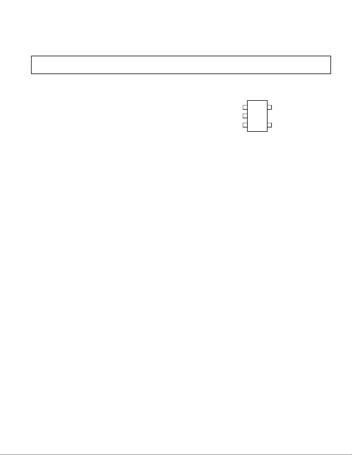
PIN CONFIGURATION
5-Lead SOT-23
SHDN
V
OUT (SENSE)
1
V
2
ADR318
IN
3
5
4
ADR318
GND
–V
OUT (FORCE)
*
*Protected by U.S. Patent No. 5,969,657; other patents pending.
REV. 0
Information furnished by Analog Devices is believed to be accurate and
reliable. However, no responsibility is assumed by Analog Devices for its
use, nor for any infringements of patents or other rights of third parties that
may result from its use. No license is granted by implication or otherwise
under any patent or patent rights of Analog Devices. Trademarks and
registered trademarks are the property of their respective companies.
One Technology Way, P.O. Box 9106, Norwood, MA 02062-9106, U.S.A.
Tel: 781/329-4700 www.analog.com
Fax: 781/326-8703 © 2003 Analog Devices, Inc. All rights reserved.
Page 2

ADR318–SPECIFICATIONS
ELECTRICAL CHARACTERISTICS
(TA = T
MIN
to T
,1 VIN = 5 V, unless otherwise noted.)
MAX
Parameter Symbol Conditions Min Typ Max Unit
Initial Accuracy V
Initial Accuracy Error V
Temperature Coefficient TCV
Minimum Supply Voltage Headroom V
Line Regulation ∆V
Load Regulation ∆V
Quiescent Current I
Voltage Noise e
Turn-On Settling Time t
Long Term Stability
2
Output Voltage Hysteresis V
Ripple Rejection Ratio RRR f
Short Circuit to Ground I
Shutdown Supply Current I
Shutdown Logic Input Current I
Shutdown Logic Low V
Shutdown Logic High V
NOTES
1
T
= 0°C, T
MIN
2
The long-term stability specification is noncumulative. The drift in subsequent 1,000 hour periods is significantly lower than in the first 1,000 hour period.
Specifications subject to change without notice.
MAX
= 70°C
O
OERR
IN
SY
N
R
∆V
O_HYS
SC
SHDN
LOGIC
INL
INH
O
– V
OUT
OUT
OUT
OUT
/∆V
IN
/∆I
LOADVIN
0°C to 70°C525ppm/°C
VIN = 2.5 V to 15 V 10 25 ppm/V
0°C < T
0°C < T
< 70°C
A
= 3 V, I
< 70°C
A
= 0 mA to 5 mA 100 ppm/mA
LOAD
No load 100 120 µA
0°C < T
< 70°C 140 µA
A
0.1 Hz to 10 Hz 5 µV p-p
= 60 Hz 85 dB
IN
VIN = 5.0 V 25 mA
= 15.0 V 30 mA
V
IN
1.795 1.8 1.802 V
–0.27 +0.27 %
600 mV
20 µs
50 ppm/1,000 hrs
40 ppm
3 µA
500 nA
0.8 V
2.4 V
REV. 0–2–
Page 3
ADR318
ABSOLUTE MAXIMUM RATINGS
1, 2
Supply Voltage . . . . . . . . . . . . . . . . . . . . . . . . . . . . . . . . . .18 V
Output Short-Circuit Duration
to GND . . . . . . . . . . . . . . . . . . . . . Observe Derating Curves
Storage Temperature Range
RJ Package . . . . . . . . . . . . . . . . . . . . . . . . .–65°C to +125°C
Operating Temperature Range . . . . . . . . . . . . . . . 0°C to 70°C
Junction Temperature Range
RJ Package . . . . . . . . . . . . . . . . . . . . . . . . .–65°C to +150°C
Lead Temperature Range
Soldering, 60 sec . . . . . . . . . . . . . . . . . . . . . . . . . . . . 300°C
NOTES
1
Absolute maximum ratings apply at 25°C, unless otherwise noted.
2
Stresses above those listed under Absolute Maximum Ratings may cause perma-
nent damage to the device. This is a stress rating only; functional operation of the
device at these or any other conditions above those listed in the operational
sections of this specification is not implied. Exposure to absolute maximum rating
conditions for extended periods may affect device reliability.
ORDERING GUIDE
Temperature Package Package Branding Output Devices
Model Range Description Option Information Voltage per Reel
ADR318ARJ-REEL7 0ºC to 70ºC 5-Lead SOT-23 RJ-5 R0A 1.800 V 3,000
Package Type
JA
JC
Unit
5-Lead SOT-23 (RJ) 230 146 °C/W
CAUTION
ESD (electrostatic discharge) sensitive device. Electrostatic charges as high as 4000 V readily
accumulate on the human body and test equipment and can discharge without detection. Although the
ADR318 features proprietary ESD protection circuitry, permanent damage may occur on devices
subjected to high energy electrostatic discharges. Therefore, proper ESD precautions are recommended
to avoid performance degradation or loss of functionality.
REV. 0
–3–
Page 4

ADR318–Typical Performance Characteristics
–
1.802
1.801
– V
1.800
OUT
V
1.799
1.798
010
20 30 40 50 60 70
TEMPERATURE – ⴗC
TPC 1. Typical Output Voltage
vs. Temperature
0
–5
–10
–15
–20
LINE REGULATION – ppm/mV
110
70ⴗC
100
25ⴗC
90
0ⴗC
80
SUPPLY CURRENT – A
70
2.5 5.0 15.0
7.5 10.0 12.5
INPUT VOLTAGE – V
TPC 2. Supply Current vs.
Input Voltage
2.5
2.3
0ⴗC
– V
2.1
IN_MIN
V
1.9
70ⴗC
25ⴗC
30
–40
–50
–60
–70
LOAD REGULATION – ppm/mA
–80
010
10V
2.5V
20 30 40 50 60 70
TEMPERATURE – ⴗC
TPC 3. Load Regulation vs.
Temperature
VOLTA GE – 2mV/DIV
–25
010
20 30 40 50 60 70
TEMPERATURE – ⴗC
TPC 4. Line Regulation vs.
Temperature
VOLTA GE – 10mV/DIV
TIME – 10ms/DIV
TPC 7. Typical Output Voltage
Noise 10 Hz to 10 kHz
1.7
012
LOAD CURRENT – mA
345
TPC 5. Minimum Input Voltage
vs. Load Current
VOLTA GE – 50mV/DIV
TIME – 40s/DIV
TPC 8. Line Transient
Response, C
BYPASS
= 0 µF
TIME – 400ms/DIV
TPC 6. Typical Output Voltage
Noise 0.1 Hz to 10 Hz
VOLTA GE – 50mV/DIV
TIME – 40s/DIV
TPC 9. Line Transient
Response, C
BYPASS
= 0.1 µF
REV. 0–4–
Page 5

ADR318
LOAD OFF LOAD ON
VOLTA GE – 200mV/DIV
TIME – 200s/DIV
TPC 10. Load Transient Response,
= 0 nF
C
L
V
IN
V
VOLTA GE – 50mV/DIV
OUT
TIME – 40s/DIV
TPC 13. Turn On/Turn Off
= 1.8 k
Response at 5 V, R
LOAD
Ω
LOAD OFF LOAD ON
VOLTA GE – 200mV/DIV
TIME – 200s/DIV
TPC 11. Load Transient Response,
= 1 nF
C
L
V
IN
VOLTA GE – 2V/DIV
V
OUT
TIME – 100s/DIV
TPC 14. Turn On/Turn Off Response
at 5 V, R
= 1.8 kΩ, C
LOAD
BYPASS
= 0.1 µF
LOAD OFF LOAD ON
VOLTA GE – 200mV/DIV
TIME – 200s/DIV
TPC 12. Load Transient Response,
= 100 nF
C
L
V
OUT
VOLTA GE – 1V/DIV
SHUTDOWN PIN
TIME – 4s/DIV
TPC 15. Shutdown Pin Response
REV. 0
–5–
Page 6

ADR318
P
TT
D
A
=
−
J
JA
θ
PARAMETER DEFINITIONS
Temperature Coefficient
Temperature coefficient is the change of output voltage with
respect to operating temperature changes, normalized by the
output voltage at 25°C. This parameter is expressed in ppm/°C,
and can be determined with the following equation:
–
VT VT
TCV
ppm
O
C
°
() ()
21
OO
=
VCTT
°
25
()
O
–
×
()
21
6
10
×
(1)
where:
V
(25°C) = VO at 25°C
O
V
) = VO at temperature 1
O(T1
V
) = VO at temperature 2
O(T2
Long Term Stability
Long term stability is the typical shift of output voltage at 25°C
on a sample of parts subjected to a test of 1,000 hours at 25°C:
∆∆VVtVt
=
()−()
OO O
V ppm
O
01
Vt Vt
()−()
OO
01
=
[]
Vt
O
()
0
6
(2)
×
10
where:
V
) = VO at 25°C at time 0
O(t0
V
) = VO at 25°C after 1,000 hours operation at 25°C
O(t1
Thermal Hysteresis
Thermal hystereses is defined as the change of output voltage
after the device is cycled through temperature from +25°C to
–40°C to +125°C and back to +25°C. This is a typical value from a
sample of parts put through such a cycle.
VVCV
OHYS OOTC
__
V ppm
OHYS
_
25
=°
[]
−
()
°
25
VCV
()
OOTC
=
VC
O
−
_
10
25
°
()
×
6
(3)
where:
V
(25°C) = VO at 25°C
O
V
= VO at 25°C after temperature cycle at +25°C to –40°C
O_TC
to +125°C and back to +25°C
THEORY OF OPERATION
Band gap references are the high performance solution for low
supply voltage and low power voltage reference applications,
and the ADR318 is no exception. The uniqueness of this product
lies in its architecture. By observing Figure 1, the ideal zero TC
band gap voltage is referenced to the output, not to ground.
Therefore, if noise exists on the ground line, it will be greatly
attenuated on V
. The band gap cell consists of the PNP pair
OUT
Q51 and Q52, running at unequal current densities. The difference
results in a voltage with a positive TC that is amplified by
in V
BE
the ratio of 2 ⫻ R58/R54. This PTAT voltage, combined with
s of Q51 and Q52, produces the stable band gap voltage.
the V
BE
Reduction in band gap curvature is performed by the ratio of
the resistors R44 and R59, one of which is linearly temperature
dependent. Precision laser trimming and other patented circuit
techniques are used to further enhance the drift performance.
V
IN
SHDN
Q1
R59
R54
R60
Q51
R44
R49R58
R53
Q52
R48
R61
V
OUT(FORCE)
V
OUT(SENSE)
GND
Figure 1. Simplified Schematic
Device Power Dissipation Considerations
The ADR318 is capable of delivering load currents up to 5 mA
with an input voltage that ranges from 2.4 V to 15 V. When this
device is used in applications with high input voltages, care should
be taken to avoid exceeding the specified maximum power dissipation or junction temperature that could result in premature
device failure. The following formula should be used to calculate
the device’s maximum junction temperature or dissipation:
(4)
In Equation 4, T
ambient temperatures, P
is the device package thermal resistance.
θ
JA
and TA are, respectively, the junction and
J
is the device power dissipation, and
D
Shutdown Mode Operation
The ADR318 includes a shutdown feature that is TTL/CMOS
compatible. A logic LOW or a 0 V condition on the SHDN pin
is required to turn the device off. During shutdown, the output
of the reference becomes a high impedance state where its potential
would then be determined by external circuitry. If the shutdown
feature is not used, the SHDN pin should be connected to V
IN
(Pin 2).
REV. 0–6–
Page 7

ADR318
APPLICATIONS
Basic Voltage Reference Connection
The circuit in Figure 2 illustrates the basic configuration for the
ADR318. Decoupling capacitors are not required for circuit stability.
The ADR318 is capable of driving capacitative loads from 0 µF to
10 µF. However, a 0.1 µF ceramic output capacitor is recommended
to absorb and deliver the charge as is required by a dynamic load.
SHUTDOWN
INPUT
SHDN
V
C
0.1F
I
IN
V
OUT(S)
ADR318
V
GND
OUT(F)
C
O
OUTPUT
0.1F
Figure 2. Voltage Reference Connection
Precision Negative Voltage Reference without Precision Resistors
A negative reference can be easily generated by combining the
ADR318 with an op amp. Figure 3 shows this simple negative
reference configuration. V
OUT(F)
and V
are at virtual ground
OUT(S)
and therefore the negative reference can be taken directly from
the output of the op amp. The op amp should be a dual-supply,
low offset, rail-to-rail amplifier, such as the OP1177.
General-Purpose Current Source
Many times in low power applications, the need arises for a precision current source that can operate on low supply voltages. As
shown in Figure 4, the ADR318 can be configured as a precision
current source. The circuit configuration illustrated is a floating
current source with a grounded load. The reference’s output voltage
is bootstrapped across R1, which sets the output current into the
load. With this configuration, circuit precision is maintained for
load currents in the range from the reference’s supply current,
typically 90 mA to approximately 5 mA. The supply current is a
function of I
and will increase slightly at a given I
SET
+V
DD
V
GND
IN
V
V
ADR318
OUT(F)
OUT(S)
I
SY (ISET
)
0.1F
R1
I
SY
ADJ
I
OUT = ISET
R
L
U1
SHDN
I
SET
+ I
SET
SV (ISET
.
)
+V
DD
ADR318
V
IN
V
OUT(F)
V
SHDN
OUT(S)
GND
OP1177
–V
SS
Figure 3. Negative Reference
Figure 4. General-Purpose Current Source
–VREF
REV. 0
–7–
Page 8

ADR318
High Power Performance with Current Limit
In some cases, the user may want higher output current delivered
to a load and still achieve better than 0.5% accuracy out of the
ADR318. The accuracy for a reference is normally specified on
the data sheet with no load. However, the output voltage changes
with load current.
The circuit in Figure 5 provides high current without compromising the accuracy of the ADR318. The power BJT Q1 provides
the required current, up to a 1 A. The ADR318 delivers the base
drive to Q1 through the force pin. The sense pin of the ADR318
is a regulated output and is connected to the load.
The transistor Q2 protects Q1 during short circuit limit faults by
robbing its base drive. The maximum current is I
V
IN
OUT(S)
ADR318
V
IN
V
GND
OUT(F)
Q2
R1
4.7k⍀
SHDN
V
L, MAX
R
S
R
L
= 0.6 V/RS.
Q1
A similar circuit function can also be achieved using the Darlington
transistor configuration, as shown in Figure 6.
V
IN
OUT(S)
ADR318
V
IN
V
OUT(F)
GND
Q1
R
S
R
L
R1Q24.7k⍀
SHDN
V
Figure 6. High Output Current with Darlington
Drive Configuration
C03431–0–1/03(0)
Figure 5. High Power Performance with Current Limit
OUTLINE DIMENSIONS
5-Lead Plastic Surface-Mount Package [SOT-23]
Dimensions shown in millimeters
2.90 BSC
4 5
1.60 BSC
1 3
2
PIN 1
1.30
1.15
0.90
0.15 MAX
1.90
BSC
0.50
0.30
COMPLIANT TO JEDEC STANDARDS MO-178AA
(RJ-5)
2.80 BSC
0.95 BSC
1.45 MAX
SEATING
PLANE
0.22
0.08
10ⴗ
PRINTED IN U.S.A.
0ⴗ
0.60
0.45
0.30
–8–
REV. 0
 Loading...