

Page 1

Precision Series Sub-Band Gap
www.BDTIC.com/ADI
FEATURES
Initial accuracy
A grade: +
B grade: +
Maximum temperature coefficient
A grade: 50 ppm/°C
B grade: 25 ppm/°C
C
= 50 nF to 10 µF
LOAD
Output current: +4 mA/−2 mA
Low operating current: 80 A (typical)
Output noise: 6 µV p-p @ 1.0 V output
Input range: 2.0 V to 18 V
Temperature range: −40°C to +125°C
Tiny, Pb-free TSOT package
APPLICATIONS
Battery-powered instrumentation
Portable medical equipment
Communication infrastructure equipment
0.70% (maximum)
0.35% (maximum)
Voltage Reference
ADR130
PIN CONFIGURATION
1
NC
ADR130
TOP VIEW
2
GND
(Not to Scale)
3
V
IN
NC = NO CONNECT
Figure 1. 6-Lead TSOT (UJ-6)
NC
6
5
SET
4
V
OUT
06322-001
GENERAL DESCRIPTION
The ADR130 is the industry’s first family of tiny, micropower,
low voltage, high precision voltage references. Featuring 0.35%
initial accuracy and 25 ppm/°C of temperature drift in the tiny
TSOT-23 package, the ADR130 voltage reference only requires
80 μA for typical operation. The ADR130 design includes a
patented temperature drift curvature correction technique that
minimizes the nonlinearities in the output voltage vs. temperature characteristics.
Available in the industrial temperature range of −40°C to
+125°C, the ADR130 is housed in a tiny TSOT package.
For 0.5 V output, tie SET (Pin 5) to V
(Pin 4). For 1.0 V
OUT
output, tie SET (Pin 5) to GND (Pin 2).
Rev. 0
Information furnished by Analog Devices is believed to be accurate and reliable. However, no
responsibility is assumed by Anal og Devices for its use, nor for any infringements of patents or ot her
rights of third parties that may result from its use. Specifications subject to change without notice. No
license is granted by implication or otherwise under any patent or patent rights of Analog Devices.
Trademarks and registered trademarks are the property of their respective owners.
One Technology Way, P.O. Box 9106, Norwood, MA 02062-9106, U.S.A.
Tel: 781.329.4700 www.analog.com
Fax: 781.461.3113 ©2006 Analog Devices, Inc. All rights reserved.
Page 2

ADR130
www.BDTIC.com/ADI
TABLE OF CONTENTS
Features .............................................................................................. 1
Applications....................................................................................... 1
Pin Configuration............................................................................. 1
General Description......................................................................... 1
Revision History ............................................................................... 2
Specifications..................................................................................... 3
Electrical Characteristics............................................................. 3
Absolute Maximum Ratings............................................................ 5
Thermal Resistance ...................................................................... 5
ESD Caution.................................................................................. 5
Typical Performance Characteristics ............................................. 6
Te r mi n ol o g y .................................................................................... 11
REVISION HISTORY
10/06—Revision 0: Initial Version
Theory of Operation ...................................................................... 12
Power Dissipation Considerations ........................................... 12
Input Capacitor........................................................................... 12
Output Capacitor........................................................................ 12
Application Notes........................................................................... 13
Basic Voltage Reference Connection....................................... 13
Stacking Reference ICs for Arbitrary Outputs ....................... 13
Negative Precision Reference Without Precision Resistors.. 14
Precision Current Source .......................................................... 14
Outline Dimensions ....................................................................... 15
Ordering Guide .......................................................................... 15
Rev. 0 | Page 2 of 16
Page 3
ADR130
www.BDTIC.com/ADI
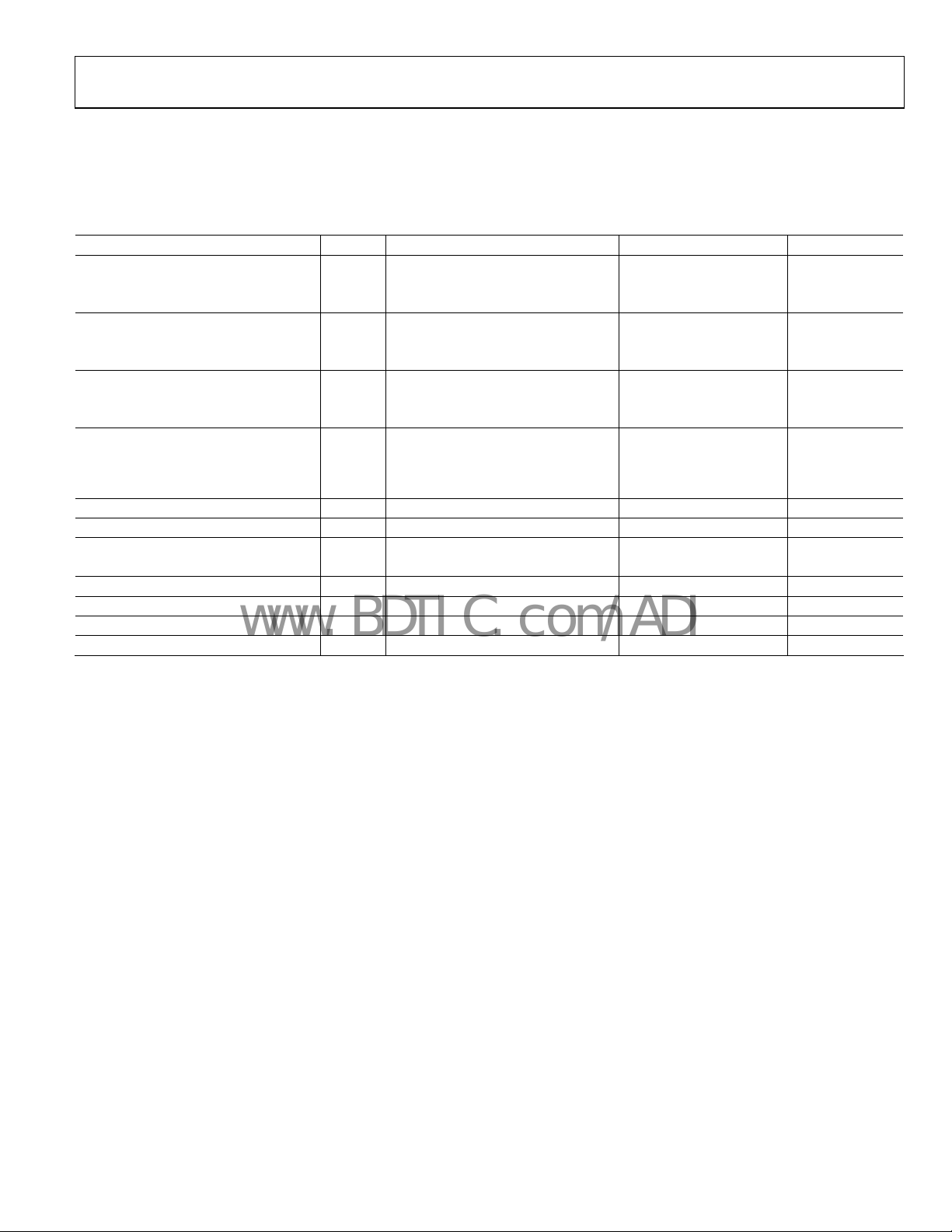
SPECIFICATIONS
ELECTRICAL CHARACTERISTICS
TA = 25°C, VIN = 2.0 V to 18 V, unless otherwise noted. SET (Pin 5) tied to V
Table 1.
Parameter Symbol Conditions Min Typ Max Unit
OUTPUT VOLTAGE V
A Grade 0.49650 0.5 0.50350 V
B Grade 0.49825 0.5 0.50175 V
INITIAL ACCURACY ERROR V
A Grade −3.50 +3.50 mV
B Grade −1.75 +1.75 mV
TEMPERATURE COEFFICIENT TCV
A Grade 15 50 ppm/°C
B Grade 5 25 ppm/°C
LOAD REGULATION
LINE REGULATION 2.0 V to 18 V, I
QUIESCENT CURRENT I
SHORT-CIRCUIT CURRENT TO GROUND VIN = 2.0 V 15 mA
V
VOLTAGE NOISE 0.1 Hz to 10 Hz 3 μV p-p
TURN-ON SETTLING TIME To 0.1%, CL = 0.1 μF 80 μs
LONG-TERM STABILITY 1000 hours @ 25°C 100 ppm/1000 hours
OUTPUT VOLTAGE HYSTERESIS 150 ppm
O
OERR
Q
−40°C < TA < +125°C
O
−40°C < T
0 mA < I
−40°C < T
−2 mA < I
−40°C < TA < +125°C, no load 75 150 μA
IN
< +125°C; 3 V ≤ VIN ≤ 18 V;
A
< 4 mA
OUT
< +125°C; 3 V ≤ VIN ≤ 18 V;
A
< 0 mA
OUT
= 0 mA −40 +10 +40 ppm/V
OUT
= 18.0 V 50 mA
(Pin 4).
OUT
−0.13 +0.13 mV/mA
−1.0 +1.0 mV/mA
Rev. 0 | Page 3 of 16
Page 4
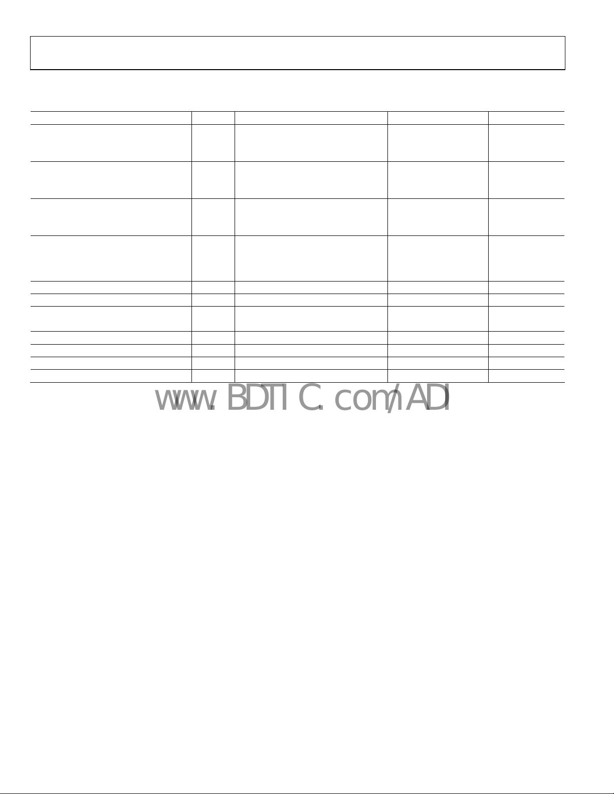
ADR130
www.BDTIC.com/ADI
TA = 25°C, VIN = 2.0 V to 18 V, unless otherwise noted. SET (Pin 5) tied to GND (Pin 2).
Table 2.
Parameter Symbol Conditions Min Typ Max Unit
OUTPUT VOLTAGE V
O
A Grade 0.9930 1.0 1.0070 V
B Grade 0.9965 1.0 1.0035 V
INITIAL ACCURACY ERROR V
OERR
A Grade −7.0 +7.0 mV
B Grade −3.5 +3.5 mV
TEMPERATURE COEFFICIENT TCV
A Grade 15 50 ppm/°C
B Grade 5 25 ppm/°C
LOAD REGULATION
LINE REGULATION 2.0 V to 18 V, I
QUIESCENT CURRENT I
Q
SHORT-CIRCUIT CURRENT TO GROUND VIN = 2.0 V 15 mA
V
VOLTAGE NOISE 0.1 Hz to 10 Hz 6 μV p-p
TURN-ON SETTLING TIME To 0.1%, CL = 0.1 μF 80 μs
LONG-TERM STABILITY 1000 hours @ 25°C 100 ppm/1000 hours
OUTPUT VOLTAGE HYSTERESIS 150 ppm
−40°C < TA < +125°C
O
−40°C < T
0 mA < I
−40°C < T
−2 mA < I
< +125°C; 3 V ≤ VIN ≤ 18 V;
A
< 4 mA
OUT
< +125°C; 3 V ≤ VIN ≤ 18 V;
A
< 0 mA
OUT
= 0 mA −40 +10 +40 ppm/V
OUT
−0.25 +0.25 mV/mA
−2.0 +2.0 mV/mA
−40°C < TA < +125°C, no load 85 150 μA
= 18.0 V 50 mA
IN
Rev. 0 | Page 4 of 16
Page 5
ADR130
www.BDTIC.com/ADI
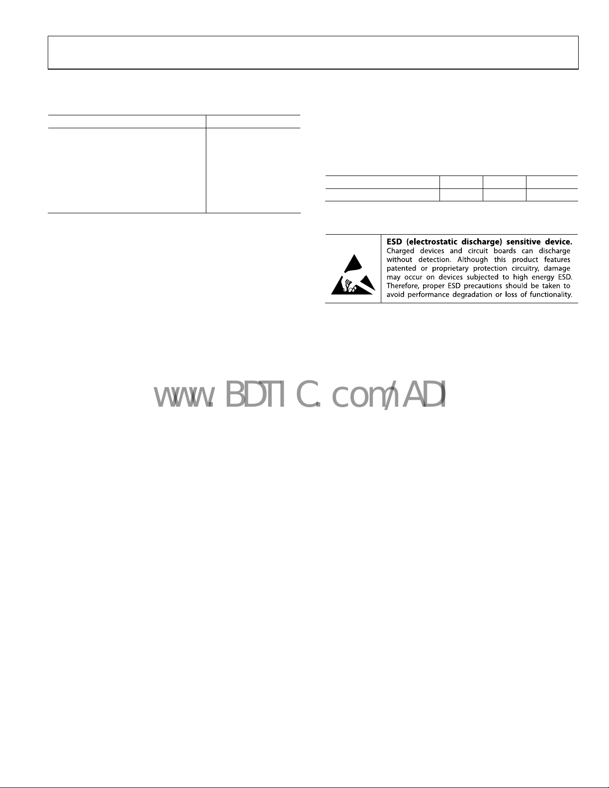
ABSOLUTE MAXIMUM RATINGS
Table 3.
Parameter Ratings
VIN to GND 20 V
Internal Power Dissipation 40 mW
Storage Temperature Range −65°C to +150°C
Specified Temperature Range −40°C to +120°C
Lead Temperature, Soldering
Vapor Phase (60 sec) 215°C
Infrared (15 sec) 220°C
Stresses above those listed under Absolute Maximum Ratings
may cause permanent damage to the device. This is a stress
rating only; functional operation of the device at these or any
other conditions above those indicated in the operational
section of this specification is not implied. Exposure to absolute
maximum rating conditions for extended periods may affect
device reliability.
THERMAL RESISTANCE
θJA is specified for the worst-case conditions, that is, a device
soldered in a circuit board for surface-mount packages.
Table 4. Thermal Resistance
Package Type θ
TSOT (UJ-6) 186 67 °C/W
JA
θ
JC
Unit
ESD CAUTION
Rev. 0 | Page 5 of 16
Page 6

ADR130
www.BDTIC.com/ADI
TYPICAL PERFORMANCE CHARACTERISTICS
0.5020
1.004
0.5015
0.5010
0.5005
(V)
0.5000
OUT
V
0.4995
0.4990
0.4985
0.4980
–40–25–105 203550658095110125
Figure 2. V
10
9
8
7
6
5
4
NUMBER OF PARTS
3
2
1
0
–50 –45 –40 –35–30 –25–20 –15–10 –5 0 5 10 15 20 25 30 35 40 45 50
Figure 3. Temperature Coefficient, V
TEMPERATURE ( °C)
vs. Temperature, V
OUT
TEMPERATURE CO EFFICI ENT (pp m/°C)
OUT
OUT
= 0.5 V
= 0.5 V
1.003
1.002
1.001
(V)
1.000
OUT
V
0.999
0.998
0.997
06322-002
06322-003
0.996
–40 –25 –10 5 20 35 50 65 80 95 110 125
Figure 5. V
10
9
8
7
6
5
4
NUMBER OF PARTS
3
2
1
0
–50 –45–40 –35–30 –25–20 –15–10 –5 0 5 10 15 20 25 30 35 40 45 50
Figure 6. Temperature Coefficient, V
TEMPERATURE ( °C)
vs. Temperature, V
OUT
TEMPERATURE CO EFFICI ENT (ppm/°C)
OUT
= 1 V
OUT
= 1 V
06322-005
06322-006
2.0
–40°C
1.8
1.6
(V)
IN_MIN
V
1.4
1.2
1.0
–2–1012345
Figure 4. Minimum Input Voltage vs. Load Current, V
+125°C
LOAD CURRENT (mA)
+25°C
OUT
06322-004
= 0.5 V
Rev. 0 | Page 6 of 16
2.0
–40°C
1.8
1.6
(V)
IN_MIN
V
1.4
1.2
1.0
–2–1012345
LOAD CURRENT (mA)
+125°C
Figure 7. Minimum Input Voltage vs. Load Current, V
+25°C
OUT
06322-007
= 1 V
Page 7

ADR130
www.BDTIC.com/ADI
160
140
120
100
+125°C
+25°C
–40°C
80
160
140
120
100
+125°C
+25°C
–40°C
80
60
SUPPLY CURRENT ( µA)
40
20
0
23456789101112131415161718
Figure 8. Supply Current vs. Input Voltage, V
6
TA = –40°C, +25° C, +125°C
5
4
3
2
SUPPLY CURRENT (mA)
1
0
–2–1012345
Figure 9. Supply Current vs. Load Current, V
INPUT VOLTAGE (V)
LOAD CURRENT (mA)
OUT
OUT
= 0.5 V
= 0.5 V
60
SUPPLY CURRENT ( µA)
40
20
06322-008
06322-009
0
23456789101112131415161718
Figure 11. Supply Current vs. Input Voltage, V
6
TA = –40°C, +25° C, +125°C
5
4
3
2
SUPPLY CURRENT (mA)
1
0
–2 012345
–1
Figure 12. Supply Current vs. Load Current, V
INPUT VOLTAGE (V)
LOAD CURRENT (mA)
OUT
OUT
= 1 V
= 1 V
06322-011
06322-012
10
VIN = 2V TO 18V
8
6
4
LINE REGULATION (ppm/V)
2
0
–40 –25 –10 5 20 35 50 65 80 95 110 12 5
Figure 10. Line Regulation
TEMPERATURE ( °C)
vs. Temperature, V
OUT
= 0.5 V
06322-010
Rev. 0 | Page 7 of 16
10
VIN = 2V TO 18V
8
6
4
LINE REGULATION (ppm/V)
2
0
–40 –25 –10 5 20 35 50 65 80 95 110 125
Figure 13. Line Regulation
TEMPERATURE ( °C)
vs. Temperature, V
OUT
06322-013
= 1 V
Page 8

ADR130
V
V
www.BDTIC.com/ADI
0.05
0.04
0.08
0.07
0.06
0.03
0.02
0.01
LOAD REGULATION–SO URCE (mV/mA)
0
–40 –25 –10 5 20 35 50 65 80 95 110 125
TEMPERATURE ( °C)
Figure 14. Load Regulation (Source) vs. Temperature, V
1.0
0.9
0.8
0.7
0.6
0.5
0.4
0.3
0.2
LOAD REGULAT ION–SINK (mV/mA)
0.1
0
–40 –25 –10 5 20 35 50 65 80 95 110 125
TEMPERATURE ( °C)
Figure 15. Load Regulation (Sink) vs. Temperature, V
OUT
OUT
= 0.5 V
= 0.5 V
0.05
0.04
0.03
0.02
0.01
LOAD REGULATION–SOURCE (mV/mA)
06322-014
06322-015
0
–40 –25 –10 5 20 35 50 65 80 95 110 125
TEMPERATURE ( °C)
Figure 17. Load Regulation (Source) vs. Temperature, V
2.0
1.8
1.6
1.4
1.2
1.0
0.8
0.6
0.4
LOAD REGULATION–SINK (mV/mA)
0.2
0
–40 –25 –10 5 20 35 50 65 80 95 110 125
TEMPERATURE ( °C)
Figure 18. Load Regulation (Sink) vs. Temperature, V
OUT
OUT
06322-017
= 1 V
06322-018
= 1 V
CIN = C
2µV/DI
= 0.1µF
OUT
CH1 PEAK-TO-PEAK 3.16µV
TIME (1s/DIV)
Figure 16. 0.1 Hz to 10 Hz Noise, V
OUT
06322-016
= 0.5 V
Rev. 0 | Page 8 of 16
CIN = C
2µV/DI
= 0.1µF
OUT
CH1 PEAK-TO- PEAK 5.72µV
TIME (1s/ DIV)
Figure 19. 0.1 Hz to 10 Hz Noise, V
OUT
06322-019
= 1 V
Page 9

ADR130
V
V
www.BDTIC.com/ADI
PEAK-TO-PEAK
CIN = C
OUT
= 0.1µF
CH1 PEAK-TO-PEAK 172µV
CIN = C
OUT
= 0.1µF
291µV
50µV/DI
Figure 20. 10 Hz to 10 kHz Noise, V
C
= C
= 0.1µF
IN
OUT
VIN = 1V/DIV
V
200mV/DIV
OUT
TIME (40µ s/DIV)
Figure 21. Turn-On Response, V
TIME (1s/DIV)
OUT
OUT
= 0.5 V
= 0.5 V
50µV/DI
06322-020
Figure 23. 10 Hz to 10 kHz Noise, V
C
= C
= 0.1µF
IN
OUT
VIN = 1V/DIV
V
= 500mV/DIV
OUT
06322-021
Figure 24. Turn-On Response, V
TIME (1s/ DIV)
TIME (40µs/DIV)
OUT
OUT
= 1 V
= 1 V
06322-023
06322-024
VIN = 1V/DIV
C
= C
= 0.1µF
IN
OUT
V
= 200mV/DIV
OUT
TIME (10ms/DIV)
Figure 22. Turn-Off Response, V
OUT
06322-022
= 0.5 V
C
= C
= 0.1µF
IN
OUT
VIN = 1V/DIV
V
= 500mV/DIV
OUT
TIME (400µs/DIV)
Figure 25. Turn-Off Response, V
OUT
06322-025
= 1 V
Rev. 0 | Page 9 of 16
Page 10

ADR130
www.BDTIC.com/ADI
VIN = 1V/DIV
C
= C
= 0.1µF
IN
= C
IN
VIN = 1V/DIV
V
OUT
OUT
= 0.1µF
= 20mV/DIV
TIME (100µ s/DIV)
C
Figure 26. Line Transient Response, V
V
= 0.5V/DIV
LOAD
= C
IN
LOAD
= 0.1µF
OUT
= 125Ω
I
LOAD
C
R
= 4mA
OUT
I
LOAD
06322-026
= 0.5 V
= 0mA
OUT
V
= 20mV/DIV
OUT
TIME (100µ s/DIV)
Figure 29. Line Transient Response, V
V
= 1V/DIV
LOAD
= C
IN
LOAD
= 0.1µF
OUT
= 250Ω
I
LOAD
= 4mA
C
R
I
LOAD
OUT
06322-029
= 1 V
= 0mA
V
= 20mV/DIV
OUT
TIME (40µ s/DIV)
Figure 27. Load Transient Response (Source), V
V
= 200mV/DIV
LOAD
C
= C
= 0.1µF
IN
R
V
LOAD
OUT
OUT
= 125Ω
= 100mV/DIV
TIME (40µ s/DIV)
I
LOAD
= 0mA
I
LOAD
Figure 28. Load Transient Response (Sink), V
OUT
= 2mA
= 0.5 V
OUT
= 0.5 V
V
= 20mV/DIV
OUT
06322-027
Figure 30. Load Transient Response (Source), V
V
OUT
06322-028
Figure 31. Load Transient Response (Sink), V
TIME (40µs/DIV)
V
= 500mV/DIV
LOAD
= C
C
IN
OUT
= 250Ω
R
LOAD
= 100mV/DIV
TIME (40µ s/DIV)
= 0.1µF
I
LOAD
I
LOAD
= 0mA
OUT
= 2mA
OUT
06322-030
= 1 V
06322-031
= 1 V
Rev. 0 | Page 10 of 16
Page 11

ADR130
()(
)
(
(
)
−=Δ
(
www.BDTIC.com/ADI
TERMINOLOGY
Temperature Coefficient
Temperature coefficient is the change of output voltage with
espect to the operating temperature change normalized by the
r
output voltage at 25°C. This parameter is expressed in ppm/°C
and is determined by
TVTV
−
[]
TCV
O
Cppm/ ×
O
=°
()
O
2
C25
1
O
()
−×°
6
10
TTV
12
where:
V
(25°C) = VO at 25°C.
O
VO(T1) = V
V
O(T2
at Temperature 1.
O
) = VO at Temperature 2.
Line Regulation
Line regulation is the change in the output due to a specified
change in input voltage. This parameter accounts for the effects
of self-heating. Line regulation is expressed in either %/V,
ppm/V, or µV/∆V
.
IN
Load Regulation
Load regulation is the change in output voltage due to a
specified change in load current. This parameter accounts for
the effects of self-heating. Load regulation is expressed in either
mV/mA, ppm/mA, or dc output resistance (Ω).
Long-Term Stability
Long-term stability is the typical shift of output voltage at 25°C
on a sample of parts subjected to a test of 1000 hours at 25°C.
)
tVtVV
OO
[]
V
O
0
=Δ
1
O
()
tVtV
)
−
()
tV
0
O
1
O
6
10ppm ×
0
O
where:
VO(t0) = V
VO(t1) = V
at 25°C at Time 0.
O
at 25°C after 1000 hours operating at 25°C.
O
Thermal Hysteresis
Thermal hysteresis is the change of output voltage after the
device is cycled through temperatures from +25°C to −40°C to
+125°C, then back to +25°C. This is a typical value from a
sample of parts put through such a cycle.
where:
V
(25°C) = VO at 25°C.
O
V
= VO at 25°C after temperature cycle from +25°C to −40°C
OTC
to +125°C, then back to +25°C.
Rev. 0 | Page 11 of 16
Page 12

ADR130
www.BDTIC.com/ADI
THEORY OF OPERATION
The ADR130 sub-band gap reference is the high performance
solution for low supply voltage and low power applications. The
uniqueness of this product lies in its architecture.
POWER DISSIPATION CONSIDERATIONS
The ADR130 is capable of delivering load currents to 4 mA
with an input range from 3.0 V to 18 V. When this device is
used in applications with large input voltages, care must be
taken to avoid exceeding the specified maximum power
dissipation or junction temperature, because this results in
premature device failure.
Use the following formula to calculate the maximum junction
t
emperature or dissipation:
TT
−
J
P
D
where:
T
is the junction temperature.
J
T
is the ambient temperature.
A
P
is the device power dissipation.
D
θ
is the device package thermal resistance.
JA
A
=
θ
JA
INPUT CAPACITOR
Input capacitors are not required on the ADR130. There is no
limit for the value of the capacitor used on the input, but a 1 F
to 10 F capacitor on the input improves transient response in
applications where there is a sudden supply change. An additional 0.1 F capacitor in parallel also helps reduce noise from
the supply.
OUTPUT CAPACITOR
The ADR130 requires a small 0.1 F output capacitor for
stability. Additional 0.1 F to 10 F capacitance in parallel can
improve load transient response. This acts as a source of stored
energy for a sudden increase in load current. The only parameter affected by the additional capacitance is turn-on time.
Rev. 0 | Page 12 of 16
Page 13

ADR130
www.BDTIC.com/ADI
APPLICATION NOTES
BASIC VOLTAGE REFERENCE CONNECTION
The circuits in Figure 32 and Figure 33 illustrate the basic
configuration for the ADR130 voltage reference.
ADR130
1
NC
2
GND
INPUT OUTPUT
3
V
INVOUT
0.1µF
Figure 32. Basic Configuration, V
ADR130
1
NC
2
3
0.1µF
GND
V
INVOUT
INPUT OUTPUT
Figure 33. Basic Configuration, V
SET
NC
SET
NC
6
5
4
0.1µF
06322-032
= 0.5 V
OUT
6
5
4
0.1µF
06322-033
= 1 V
OUT
STACKING REFERENCE ICs FOR ARBITRARY OUTPUTS
Some applications may require two reference voltage sources
that are a combined sum of the standard outputs. Figure 34 and
Figure 35 show how these stacked output references can be
mplemented.
i
U2
1
2
3
0.1µF
NC
ADR130
GND
V
IN
V
NC
SET
OUT
6
5
V
4
OUT2
0.1µF
0.1µF
INPUT
0.1µF
Figure 35. Stacking References with ADR130, V
Two reference ICs are used and fed from an unregulated input,
V
. The outputs of the individual ICs that are connected in
IN
series provide two output voltages, V
terminal voltage of U1, and V
the terminal voltage of U2. U1 and U2 are chosen for the two
voltages that supply the required outputs (see
mple, if U1 is set to have an output of 1 V or 0.5 V, the user
exa
can stack on top of U2 to get an output of 2 V or 1.5 V.
Table 5. Required Outputs
U1/U2 Comments V
ADR130/ADR130 See Figure 34 1 V 2 V
ADR130/ADR130 See Figure 35 0.5 V 1.5 V
1
2
3
1
2
3
U2
NC
ADR130
GND
V
IN
U1
NC
ADR130
GND
V
IN
is the sum of this voltage and
OUT2
SET
V
SET
V
OUT1
NC
OUT
NC
OUT
6
5
4
6
5
4
= 0.5 V. V
OUT1
and V
OUT2
Table 5 ). For
V
OUT2
0.1µF
V
OUT1
0.1µF
OUT1
. V
OUT2
06322-035
= 1.5 V
OUT1
is the
V
OUT2
1
U1
2
3
0.1µF
NC
ADR130
GND
V
IN
INPUT
Figure 34. Stacking References with ADR130, V
V
NC
SET
OUT
6
5
4
OUT1
V
OUT1
0.1µF
= 1.0 V, V
06322-034
OUT2
= 2.0 V
Rev. 0 | Page 13 of 16
Page 14

ADR130
V
www.BDTIC.com/ADI
NEGATIVE PRECISION REFERENCE WITHOUT PRECISION RESISTORS
A negative reference is easily generated by adding an op amp,
A1, and is configured as shown in Figure 36. V
ground and, therefore, the negative reference can be taken
directly from the output of the op amp. The op amp must be
dual-supply, low offset, and rail-to-rail if the negative supply
voltage is close to the reference output.
U2
1
NC
ADR130
2
GND
+
DD
3
V
IN
–V
REF
Figure 36. Negative Reference, −V
0.1µF
V+
A1
OP291
V–
–V
DD
V
NC
SET
OUT
REF
OUT
6
5
4
1kΩ
= −0.5 V
is at virtual
06322-036
PRECISION CURRENT SOURCE
In low power applications, the need can arise for a precision
current source that can operate on low supply voltages. The
ADR130 can be configured as a precision current source (see
Figure 37). The circuit configuration shown is a floating current
source with a grounded load. The reference output voltage is
bootstrapped across R
load. With this configuration, circuit precision is maintained for
load currents ranging from the reference supply current,
typically 85 μA, to approximately 4 mA.
V
IN
Figure 37. ADR130 as a Precision Current Source
, which sets the output current into the
SET
ADR130
1
NC
2
GND
3
V
INVOUT
NC
SET
6
5
4
R
SET
P1
R
L
06322-037
Rev. 0 | Page 14 of 16
Page 15

ADR130
R
www.BDTIC.com/ADI
OUTLINE DIMENSIONS
2.90 BSC
1.90
BSC
0.50
0.30
45
2.80 BSC
2
0.95 BSC
*
1.00 MAX
SEATING
PLANE
0.20
0.08
8°
0.60
4°
0.45
0°
0.30
1.60 BSC
PIN 1
INDICATO
*
0.90
0.87
0.84
0.10 MAX
6
13
*
COMPLIANT TO JEDEC STANDARDS MO-193-AA WITH
THE EXCEPTION OF PACKAGE HEIGHT AND THICKNESS.
Figure 38. 6-Lead Thin Small Outline Transistor Package [TSOT]
(UJ-6)
Dim
ensions shown in millimeters
ORDERING GUIDE
Temperature Coefficient
(p
Model
pm/°C)
ADR130AUJZ-REEL7150 −40°C to +125°C 6-Lead TSOT UJ-6 R0W 3,000
ADR130AUJZ-R2
1
50 −40°C to +125°C 6-Lead TSOT UJ-6 R0W 250
ADR130BUJZ-REEL7125 −40°C to +125°C 6-Lead TSOT UJ-6 R0X 3,000
ADR130BUJZ-R2
1
Z = Pb-free part.
1
25 −40°C to +125°C 6-Lead TSOT UJ-6 R0X 250
Temperature
Range
Package
Description
Package
Option
Branding
Ordering
Quantity
Rev. 0 | Page 15 of 16
Page 16

ADR130
www.BDTIC.com/ADI
NOTES
©2006 Analog Devices, Inc. All rights reserved. Trademarks and
registered trademarks are the property of their respective owners.
D06322-0-10/06(0)
Rev. 0 | Page 16 of 16
 Loading...