

Page 1
Charge Pump Driven 9-Channel LED Driver with
09478-001
D1
D2 D3
D4 D5
D7D6
D8 D9
nRST
SDA
SCL
nINT
GND
VIN
1µF
C2+
C2–
C2
1µF
C1+
C1–
C1
1µF
VOUT
1µF
ADP8866
FEATURES
Charge pump with automatic gain selection of 1×, 1.5×, and
2× for maximum efficiency
92% peak efficiency
9 independent and programmable LED drivers
Each driver is capable of 25 mA (full scale)
Each driver has 7 bits (128 levels) of nonlinear current
settings
Standby mode for <1 µA current consumption
16 programmable fade-in and fade-out times (0.0 sec to
1.75 sec) with choice of square or cubic rates
Automated and customizable LED blinking
Unique heartbeat mode for programmable double pulse
lighting effects on 4 channels (D6 to D9)
PWM input for implementing content adjustable brightness
control (cABC)
2
I
C compatible interface for all programming
Dedicated reset pin and built-in power on reset (POR)
Short circuit, overvoltage, and overtemperature protection
Internal soft start to limit inrush currents
Input to output isolation during faults or shutdown
Operates down to V
(UVLO) at 1.9 V
Small lead frame chip scale package (LFCSP)
= 2.5 V, with undervoltage lockout
IN
Automated LED Lighting Effects
ADP8866
APPLICATIONS
Mobile display backlighting
Mobile phone keypad backlighting
LED indication and status lights
Automated LED blinking
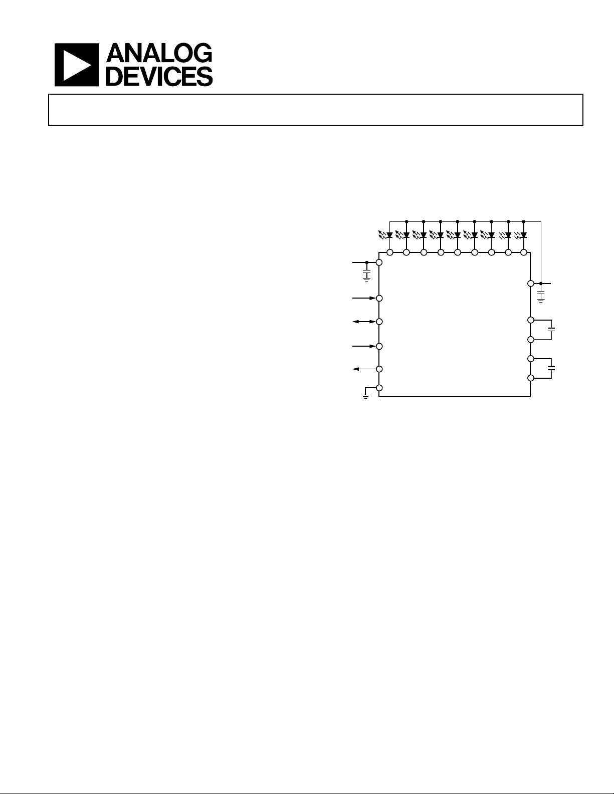
TYPICAL OPERATING CIRCUIT
Figure 1.
GENERAL DESCRIPTION
The ADP8866 combines a programmable backlight LED charge
pump driver with automatic blinking functions. Nine LED drivers
can be independently programmed at currents up to 25 mA.
The current level, fade time, and blinking rate can be programmed
once and executed autonomously on a loop. Separate fade-in
and fade-out times can be set for the backlight LEDs.
Rev. 0
Information furnished by Analog Devices is believed to be accurate and reliable. However, no
responsibility is assumed by Analog Devices for its use, nor for any infringements of patents or other
rights of third parties that may result from its use. Specifications subject to change without notice. No
license is granted by implication or otherwise under any patent or patent rights of Analog Devices.
Trademarks and registered trademarks are the property of th eir respective owners.
Driving all of this is a two-capacitor charge pump with gains of
1×, 1.5×, and 2×. This setup is capable of driving a maximum
I
of 240 mA from a supply of 2.5 V to 5.5 V. A full suite of
OUT
safety features including short-circuit, overvoltage, and overtemperature protection allows easy implementation of a safe
and robust design. Additionally, input inrush currents are
limited via an integrated soft start combined with controlled
input to output isolation.
One Technology Way, P.O. Box 9106, Norwood, MA 02062-9106, U.S.A.
Tel: 781.329.4700 www.analog.com
Fax: 781.461.3113 ©2011 Analog Devices, Inc. All rights reserved.
Page 2

ADP8866
TABLE OF CONTENTS
Features .............................................................................................. 1
Applications ....................................................................................... 1
Typical Operating Circuit ................................................................ 1
General Description ......................................................................... 1
Revision History ............................................................................... 2
Specifications ..................................................................................... 3
Absolute Maximum Ratings ............................................................ 5
Maximum Temperature Ranges ................................................. 5
Thermal Resistance ...................................................................... 5
ESD Caution .................................................................................. 5
Pin Configurations and Function Descriptions ........................... 6
Typical Performance Characteristics ............................................. 7
Theory of Operation ...................................................................... 11
Power Stage.................................................................................. 12
Operating Modes ........................................................................ 13
LED Groups................................................................................. 14
Output Current Settings ............................................................ 14
Output Current Range Selection .............................................. 14
PWM Dimming .......................................................................... 14
Automated Fade-in and Fade-Out ........................................... 14
CABC Fade Disable ................................................................... 15
Independent Sink Control (ISC) .............................................. 15
Advanced Blinking Controls .................................................... 16
Short-Circuit Protection (SCP) Mode ..................................... 17
Overvoltage Protection (OVP) ................................................. 17
Thermal Shutdown (TSD)/Overtemperature Protection ..... 17
Interrupts ..................................................................................... 19
Backlight Off Interrupt .............................................................. 19
Independent Sink Off Interrupt ............................................... 19
Applications Information .............................................................. 20
Layout Guidelines....................................................................... 20
I2C Programming and Digital Control ........................................ 21
Register Descriptions ..................................................................... 22
Backlight Register Descriptions ............................................... 29
Independent Sink Register Descriptions ................................. 34
Outline Dimensions ....................................................................... 50
Ordering Guide .......................................................................... 50
REVISION HISTORY
3/11—Revision 0: Initial Version
Rev. 0 | Page 2 of 52
Page 3

ADP8866
SPECIFICATIONS
VIN = 3.6 V, SCL = 2.7 V, SDA = 2.7 V, nINT = open, nRST = 2.7 V, V
T
= 25°C and are not guaranteed. Minimum and maximum limits are guaranteed from TJ = −40°C to +105°C, unless otherwise noted.
J
Table 1.
Parameter Symbol Test Conditions/Comments Min Typ Max Unit
SUPPLY
Input Voltage
Operating Range VIN 2.5 5.5 V
Startup Level V
Low Level V
V
Hysteresis V
IN (STA RT )
UVLO Noise Filter t
VIN increasing 1.98 2.25 V
IN (STA RT )
VIN decreasing 1.75 1.90 V
IN(STOP)
After startup 80 mV
IN(HYS)
10 μs
UVLO
Quiescent Current IQ
During Standby I
Q(STBY)
= 3.6 V, Bit nSTBY = 0, SCL = SDA =
V
IN
0 V
Current Consumption
During Blinking Off Time
Switching I
I
Q(OFF)
= 3.6 V, Bit nSTBY = 1, I
V
IN
Measured during blinking off time
VIN = 3.6 V, Bit nSTBY = 1, I
Q(ACTIVE)
Gain = 1.0× 1.2 2.0 mA
Gain = 1.5× 3.7 5.4 mA
Gain = 2.0× 4.3 6.2 mA
OSCILLATOR Charge pump gain = 2×
Switching Frequency fSW 0.8 1 1.2 MHz
Duty Cycle D 50 %
OUPUT CURRENT CONTROL
Maximum Drive Current I
D1:D9(MAX)
V
= 0.4 V
D1:D9
TJ = 25°C 23.0 25.0 27.0 mA
TJ = −40°C to +85°C 22.5 27.5 mA
LED Current Source Matching I
All Current Sinks I
D1 to D5 Current Sinks I
Leakage Current on LED Pins I
Equivalent Output Resistance R
Gain = 1× VIN = 3.6 V, I
Gain = 1.5× VIN = 3.1 V, I
Gain = 2× VIN = 2.5 V, I
Regulated Output Voltage V
MAT CH
V
MAT CH9
V
MAT CH5
VIN = 5.5 V, V
D1:D9(LKG)
OUT
VIN = 3 V, gain = 2×, I
OUT(REG)
= 0.4 V 1.4 %
D1:D9
= 0.4 V 1.1 %
D1:D5
= 2.5 V, Bit nSTBY = 1 0.5 μA
D1:D9
= 100 mA 0.5 Ω
OUT
= 100 mA 3.0 Ω
OUT
= 100 mA 3.8 Ω
OUT
AUTOMATIC GAIN SELECTION
Minimum Voltage
Gain Increases V
Minimum Current Sink
Decrease VDX until the gain switches up 145 200 240 mV
HR(UP)
V
HR(MIN)
IDX = I
× 95% 210 mV
DX(MAX)
Headroom Voltage
Gain Delay t
GAIN
The delay after gain has changed and
before gain is allowed to change again
FAULT PROTECTION
Startup Charging Current
VIN = 3.6 V, V
I
SS
= 0.8 × VIN 3.5 7 11 mA
OUT
Source
Output Voltage Threshold V
Exit Soft Start V
Short-Circuit Protection V
Output Overvoltage Protection V
OUT
V
OUT(START)
V
OUT(SC)
OVP
rising 0.92 × VIN V
OUT
falling 0.55 × VIN V
OUT
Activation Level 5.7 6.0 V
OVP Recovery Hysteresis 500 mV
= 0.4 V, C1 = 1 μF, C2 = 1 μF, C
D1:D9
= 1 μF, typical values are at
OUT
0.25 1.0 μA
= 0 mA
OUT
= 0 mA
OUT
= 10 mA 4.4 4.9 5.2 V
OUT
245 325 μA
100 μs
Rev. 0 | Page 3 of 52
Page 4
ADP8866
SDA
SCL
S
S = START CONDITION
Sr = REPEAT E D S TART CONDI TION
P = STOP CONDITION
Sr
P
S
t
LOW
t
R
t
HD, DAT
t
HIGH
t
SU, DAT
t
F
t
F
t
SU, STA
t
HD, STA
t
SP
t
SU, STO
t
BUF
t
R
09478-002
Parameter Symbol Test Conditions/Comments Min Typ Max Unit
Thermal Shutdown
Threshold TSD Increasing temperature 150 °C
Hysteresis TSD
Isolation from Input to
Output During Fault
Time to Validate a Fault t
I2C INTERFACE
V
Voltage Operating Range V
DDIO
Logic Low Input VIL VIN = 2.5 V 0.5 V
Logic High Input VIH VIN = 5.5 V 1.55 V
I2C TIMING SPECIFICATIONS Guaranteed by design
Delay from Reset Deassertion
2
C Access
to I
SCL Clock Frequency f
SCL High Time t
SCL Low Time t
Setup Time
Data t
Repeated Start t
Stop Condition t
Hold Time
Data t
Start/Repeated Start t
Bus Free Time (Stop and Start
Conditions)
Rise Time (SCL and SDA) tR 20 + 0.1 × CB 300 ns
Fall Time (SCL and SDA) tF 20 + 0.1 × CB 300 ns
Pulse Width of Suppressed
Spike
Capacitive Load Per Bus Line C
Timing Diagram
20 °C
(HYS)
VIN = 5.5 V, V
I
OUTLKG
2 μs
FAU LT
5.5 V
DDIO
20 μs
t
RESET
400 kHz
SCL
0.6 μs
HIGH
1.3 μs
LOW
100 ns
SU , DAT
0.6 μs
SU, STA
0.6 μs
SU, STO
0 0.9 μs
HD, DAT
0.6 μs
HD, STA
t
1.3 μs
BUF
0 50 ns
t
SP
B
400 pF
= 0 V, Bit nSTBY = 0 1 μA
OUT
2
Figure 2. I
C Interface Timing Diagram
Rev. 0 | Page 4 of 52
Page 5
ADP8866
ABSOLUTE MAXIMUM RATINGS
Table 2.
Parameter Rating
VIN, VOUT to GND −0.3 V to +6 V
D1, D2, D3, D4, D5, D6, D7, D8, and D9 to
−0.3 V to +6 V
GND
nINT, nRST, SCL, and SDA to GND −0.3 V to +6 V
Output Short-Circuit Duration Indefinite
Operating Ambient Temperature Range −40°C to +85°C1
Operating Junction Temperature Range −40°C to +125°C
Storage Temperature Range −65°C to +150°C
Soldering Conditions JEDEC J-STD-020
ESD (Electrostatic Discharge)
Human Body Model (HBM) ±2.0 kV
Charged Device Model (CDM) ±1.5 kV
1
The maximum operating junction temperature (T
maximum operating ambient temperature (T
Temperature Ranges section for more information.
) supersedes the
J(MAX)
). See the Maximum
A(MAX)
Stresses above those listed under Absolute Maximum Ratings
may cause permanent damage to the device. This is a stress
rating only; functional operation of the device at these or any
other conditions above those indicated in the operational section of
this specification is not implied. Exposure to absolute maximum
rating conditions for extended periods may affect device reliability.
Absolute maximum ratings apply individually only, not in
combination. Unless otherwise specified, all voltages are
referenced to GND.
THERMAL RESISTANCE
The θJA (junction to air) and θJC (junction to case) are
determined according to JESD51-9 on a 4-layer printed circuit
board (PCB) with natural convection cooling. The exposed pad
must be soldered to GND.
Table 3. Thermal Resistance
Package Type θJA θJC Unit
LFCSP 38.6 3.56 °C/W
ESD CAUTION
MAXIMUM TEMPERATURE RANGES
The maximum operating junction temperature (T
supersedes the maximum operating ambient temperature
(T
). Therefore, in situations where the ADP8866 is
A(MAX)
exposed to poor thermal resistance and a high power dissipation
(P
), the maximum ambient temperature may need to be derated.
D
In these cases, the ambient temperature maximum can be
calculated with the following equation:
T
A(MAX)
= T
J(MAX)
− (θJA × P
D(MAX)
).
J(MAX)
)
Rev. 0 | Page 5 of 52
Page 6
ADP8866
PIN CONFIGURATIONS AND FUNCTION DESCRIPTIONS
D4
D5
20
19
D8
D6
D7
16
18
17
1
D3
2
D2
D1
D9
nRST
NOTES
1. CONNECT THE EXPOSED
PADDLE TO GND.
3
4
5
ADP8866
TOP VIEW
(Not to S cale)
8
6
7
SCL
SDA
nINT
9
C1–
10
C2–
15 GND
14
VIN
13
VOUT
12
C2+
11
C1+
09478-003
Figure 3. LFCSP Pin Configuration
Table 4. Pin Function Descriptions
Pin No. Mnemonic Description
14 VIN Battery Voltage 2.5 V to 5.5 V.
3 D1 LED Sink 1 Output.
2 D2 LED Sink 2 Output.
1 D3 LED Sink 3 Output.
20 D4 LED Sink 4 Output.
19 D5 LED Sink 5 Output.
18 D6 LED Sink 6 Output.
17 D7 LED Sink 7 Output.
16 D8 LED Sink 8 Output.
4 D9 LED Sink 9 Output.
13 VOUT Charge Pump Output.
11 C1+ Charge Pump C1+.
9 C1−
Charge Pump C1−.
12 C2+ Charge Pump C2+.
10 C2− Charge Pump C2−.
15 GND Ground. Connect the exposed paddle to GND.
8 nINT
Processor Interrupt (Active Low). Requires an external pull-up resistor. If this pin is not used, it can be left
floating. Alternatively, this pin can be set as the PWM input for implementing cABC dimming (see the
PWM Dimming section).
5 nRST
Hardware Reset Input (Active Low). This bit resets the device to the default conditions. If not used, this pin
must be tied above V
IH(MAX)
.
7 SDA I2C Serial Data Input. Requires an external pull-up resistor.
6 SCL I2C Clock Input. Requires an external pull-up resistor.
Rev. 0 | Page 6 of 52
Page 7
ADP8866
1400
1200
1000
800
600
400
200
0
2.5 3.0 3.5 4.0 4.5 5.0 5.5
V
IN
(V)
I
Q
(µA)
09478-004
+105°C
+85°C
+25°C
–40°C
5.0
4.5
4.0
3.5
3.0
2.5
2.0
1.5
1.0
0.5
0
2.5 3.0 3.5 4.0 4.5 5.0 5.5
V
IN
(V)
I
Q
(mA)
09478-005
+105°C
+85°C
+25°C
–40°C
5.0
4.5
4.0
3.5
3.0
2.5
2.0
1.5
1.0
0.5
0
2.5 3.0 3.5 4.0 4.5 5.0 5.5
V
IN
(V)
I
Q
(mA)
09478-006
+105°C
+85°C
+25°C
–40°C
400
350
300
250
200
150
100
50
0
2.5 3.0 3.5 4.0 4.5 5.0 5.5
V
IN
(V)
I
Q (OFF)
(µA)
09478-007
+105°C
+85°C
+25°C
–40°C
1.0
0.9
0.8
0.7
0.6
0.5
0.4
0.3
0.2
0.1
0
2.5 3.0 3.5 4.0 4.5 5.0 5.5
V
IN
(V)
STANDBY I
Q
(µA)
09478-008
+105°C
+85°C
+25°C
–40°C
SCL = SDA = 0V
27.0
26.5
26.0
25.5
25.0
24.5
24.0
23.5
23.0
2.5 3.0 3.5 4.0 4.5 5.0 5.5
V
IN
(V)
I
LED
(mA)
09478-009
+105°C
+85°C
+25°C
–40°C
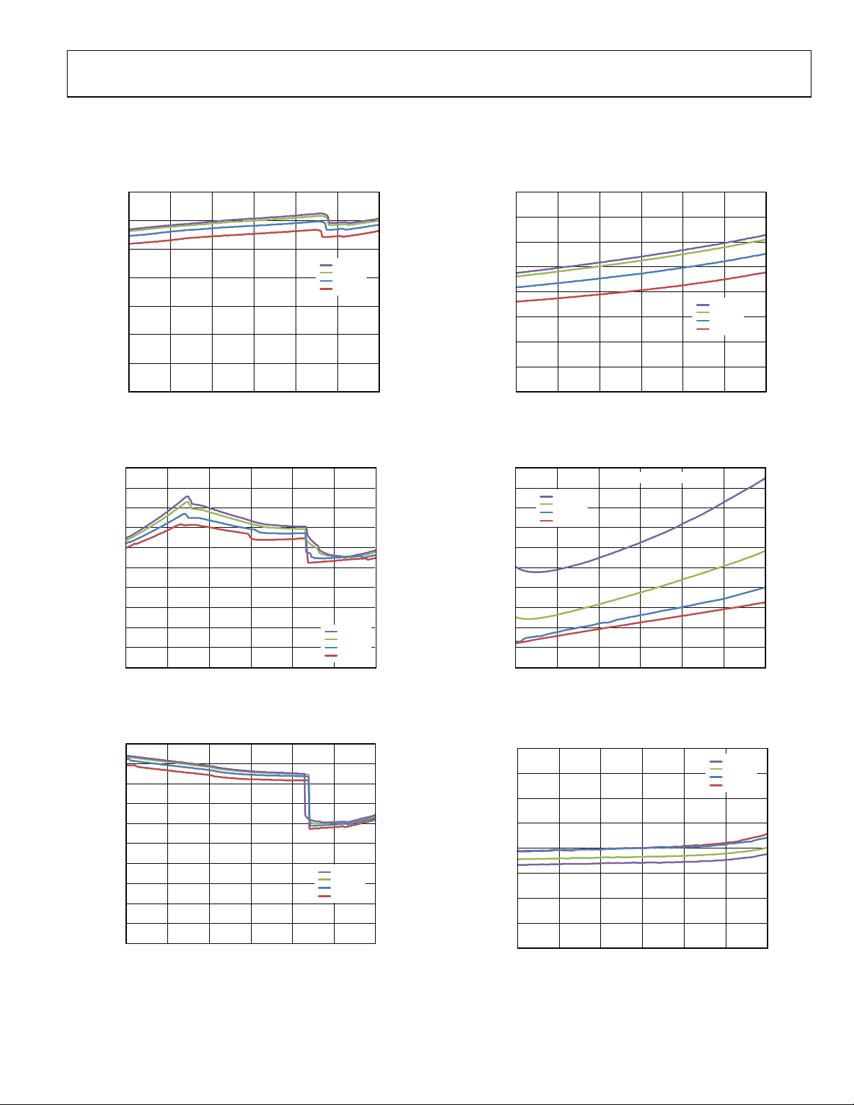
TYPICAL PERFORMANCE CHARACTERISTICS
VIN = 3.6 V, SCL = 2.7 V, SDA = 2.7 V, nRST = 2.7 V, V
unless otherwise noted.
D1:D9
= 0.4 V, I
= 0 mA, CIN = 1 μF, C1 = 1 μF, C2 = 1 μF, C
OUT
= 1 μ F, TA= 25°C,
OUT
Figure 4. Typical Operating Current, G = 1×
Figure 5. Typical Operating Current, G = 1.5×
Figure 7. Typical Off Time Current (I
Q(OFF)
)
Figure 8. Typical Standby IQ
Figure 6. Typical Operating Current, G = 2×
Figure 9. Typical Diode Current vs. VIN
Rev. 0 | Page 7 of 52
Page 8
ADP8866
1.6
1.4
1.2
1.0
0.8
0.6
0.4
0.2
0
2.5 3.0 3.5 4.0 4.5 5.0 5.5
V
IN
(V)
MATCHING ( %)
09478-010
+105°C
+85°C
+25°C
–40°C
I
D1:D9
= 25mA
26.5
26.0
25.5
25.0
24.5
24.0
23.5
27.0
23.0
0.2 0.4 0.6 0.8 1.0 1.2 1.4 1.6 1.8 2.0
V
HR
(V)
I
LED
CURRENT (mA)
09478-011
+105°C
+85°C
+25°C
–40°C
1.4
1.2
1.0
0.8
0.6
0.4
0.2
1.6
0
0.2 0.4 0.6 0.8 1.0 1.2 1.4 1.6 1.8 2.0
V
HR
(V)
MATCHING ( %)
09478-012
+105°C
+85°C
+25°C
–40°C
I
D1:D9
= 25mA
0.1
0
–0.1
–0.2
–0.3
–0.4
–0.5
–0.6
–0.7
–0.8
–40 –15 10 35 60 85 110
TEMPERATURE (°C)
I
OUT
DEVIATI ON (%)
09478-013
I
OUT
= 100mA
1.2
1.0
0.8
0.6
0.4
0.2
0
2.5 3.0 3.5 4.0 4.5 5.0 5.5
V
IN
(V)
R
OUT
(Ω)
09478-014
+105°C
+85°C
+25°C
–40°C
I
OUT
= 100mA
6
5
4
3
2
1
0
2.2 2.4 2.6 2.8 3.0 3.2 3.4
V
IN
(V)
R
OUT
(Ω)
09478-015
+105°C
+85°C
+25°C
–40°C
I
OUT
= 100mA
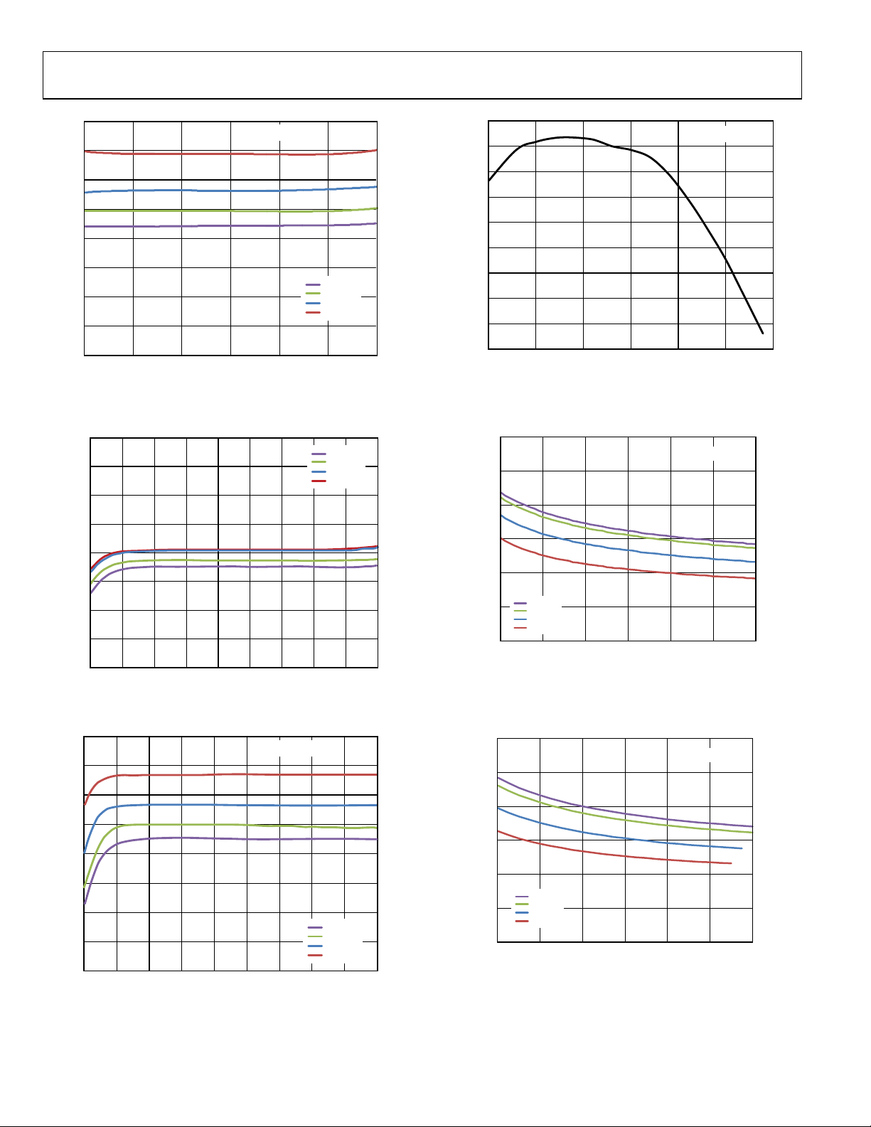
Figure 10. Typical Diode Matching vs. V
IN
Figure 13. Typical Change in Diode Current vs. Temperature
Figure 11. Typical Diode Matching vs. Current Sink Headroom Voltage (VHR)
Figure 12. Typical Diode Current vs. Current Sink Headroom Voltage (VHR)
Figure 14. Typical R
(G = 1×) vs. VIN
OUT
Figure 15. Typical R
(G = 1.5×) vs. VIN
OUT
Rev. 0 | Page 8 of 52
Page 9
ADP8866
6
5
4
3
2
1
0
2.2 2.3 2.4 2.5 2.6 2.7 2.8
V
IN
(V)
R
OUT
(Ω)
09478-016
+105°C
+85°C
+25°C
–40°C
I
OUT
= 100mA
20
18
16
14
12
10
8
6
4
2
0
2.5 3.0 3.5 4.0 4.5 5.0 5.5
V
IN
(V)
I
SS
(mA)
09478-017
+105°C
+85°C
+25°C
–40°C
VOUT = 80% OF VIN
30
25
20
15
10
5
0
0 20 40 60 80 100
PWM DUTY CYCLE (%)
AVERAGE LE D CURRE NT (mA)
09478-018
+85°C
+25°C
–40°C
1.4
1.0
1.2
0.6
0.8
0.2
0.4
0
2.5 3.0 3.5 4.0 4.5 5.0 5.5
V
IN
(V)
THRESHOL D ( V )
09478-019
VIL, +25°C
V
IH
, +25°C
V
IL
, –40°C
V
IH
, –40°C
V
IL
, +85°C
V
IH
, +85°C
V
IL
, +105°C
V
IH
, +105°C
5.3
5.2
5.1
5.0
4.9
4.8
4.7
4.6
–40 –15 10 35 60 85 110
TEMPERATURE (°C)
V
OUT(REG)
(V)
09478-020
6.0
5.9
5.8
5.7
5.6
5.5
5.4
5.3
5.2
5.1
5.0
–40 –15 10 35 60 85 110
TEMPERATURE (°C)
V
OUT
(V)
09478-021
THRESHOLD
RECOVERY
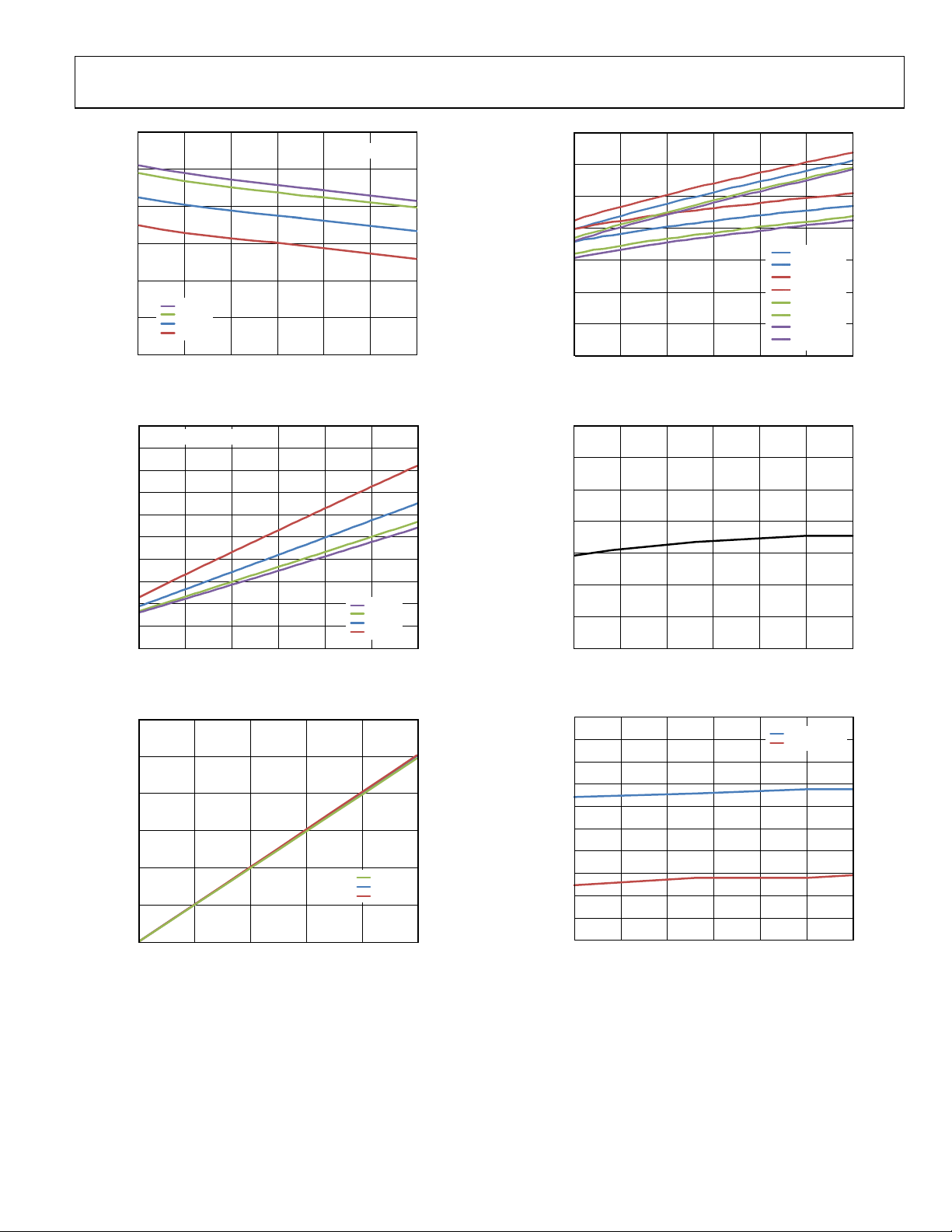
Figure 16. Typical R
(G = 2×) vs. VIN
OUT
Figure 17. Typical Output Soft Start Current, ISS
Figure 19. Typical I2C Thresholds, VIH and VIL
Figure 20. Typical Regulated Output Voltage (V
OUT(REG)
)
Figure 18. Typical Average I
OUT
vs. PWM Duty (f
= 300 Hz)
PWM
Figure 21. Typical Overvoltage Protection (OVP) Threshold
Rev. 0 | Page 9 of 52
Page 10
ADP8866
100
90
80
70
60
50
40
30
20
10
0
2.5 3.0 3.5 4.0 4.5 5.0 5.5
V
IN
(V)
EFFICIENCY (%)
09478-022
V
F
= 3.4V
V
F
= 4.0V
09478-024
1µs/DIV
1
2
3
V
IN
(AC-COUPLE D) 50mV /DIV
V
OUT
(AC-COUPLE D) 50mV /DIV
I
IN
(AC-COUPLE D) 10mA/DIV
T
C
IN
= 1µF, C
OUT
= 1µF, C1 = 1µ F, C2 = 1µF
V
IN
= 3.6V
I
OUT
= 120mA
09478-025
1µs/DIV
1
2
3
VIN (AC-COUPLE D) 50mV /DIV
V
OUT
(AC-COUPLE D) 50mV /DIV
IIN (AC-COUPLE D) 10mA/DIV
T
CIN = 1µF, C
OUT
= 1µF, C1 = 1µ F, C2 = 1µF
V
IN
= 3.0V
I
OUT
= 120mA
09478-026
1µs/DIV
1
2
3
VIN (AC-COUPLE D) 50mV /DIV
V
OUT
(AC-COUPLE D) 50mV /DIV
I
IN
(AC-COUPLE D) 10mA/DIV
T
C
IN
= 1µF, C
OUT
= 1µF, C1 = 1µ F, C2 = 1µF
V
IN
= 2.5V
I
OUT
= 120mA
09478-027
100µs/DIV
2
4
IIN (10mA/DIV)
V
OUT
(1V/DIV)
I
OUT
(10mA/DIV)
T
3
C
IN
= 10µF, C
OUT
= 1µF, C1 = 1µ F, C2 = 1µF
V
IN
= 3.6V
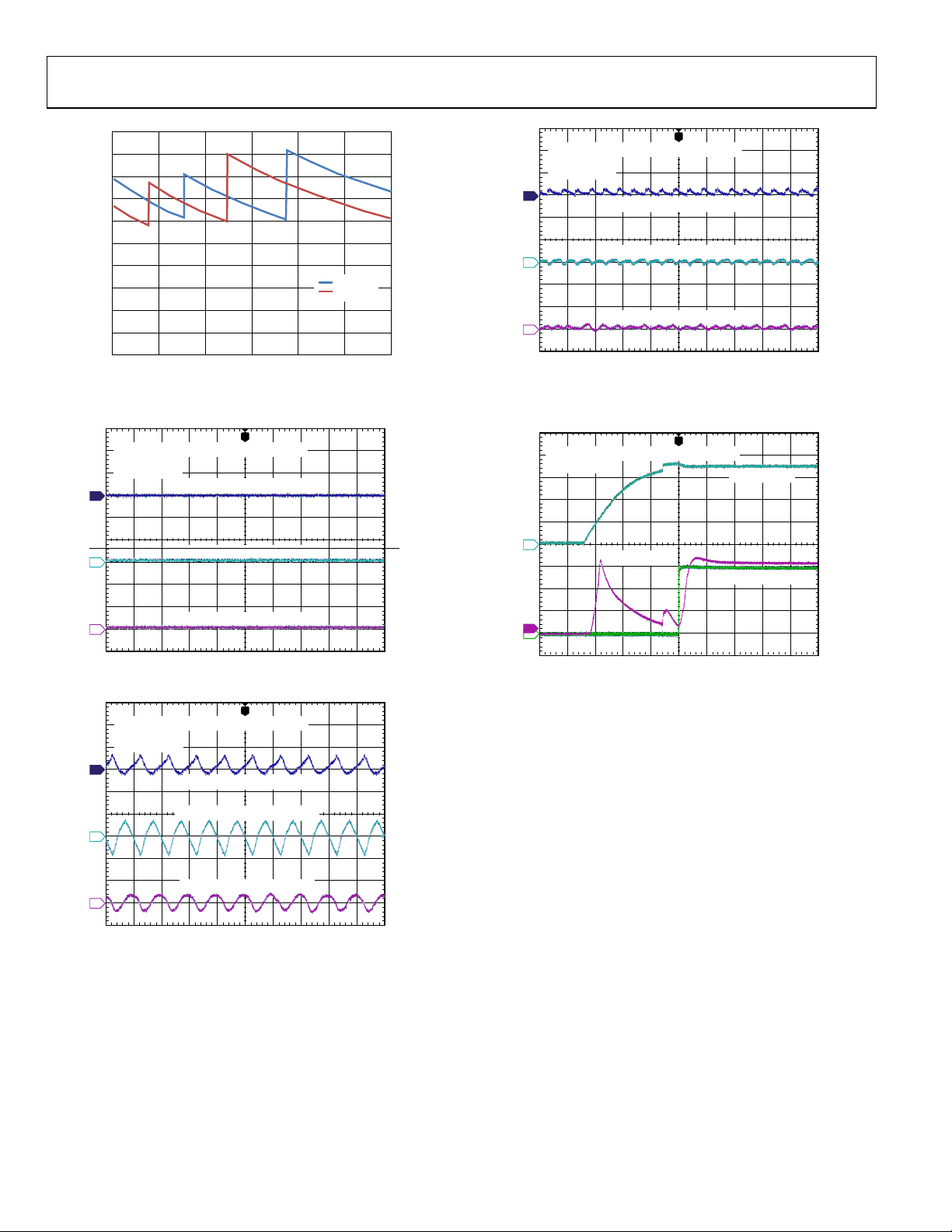
Figure 22. Typical Efficiency (Each LED Set to 25 mA)
Figure 25. Typical Operating Waveforms, G = 2×
Figure 23. Typical Operating Waveforms, G = 1×
Figure 24. Typical Operating Waveforms, G = 1.5×
Figure 26. Typical Startup Waveforms
Rev. 0 | Page 10 of 52
Page 11
ADP8866
09478-028
C1
1µF
C2
1µF
nINT
C
OUT
VOUT
C
IN
VIN
V
REFS
I
REFS
STANDBY
EN
VIN
C1+
SDA
SCL
I2C LOGIC
STANDBY
ILED CONTROL
C1–
C2+
C2–
nRST
NOISE FILTER
50µs
RESET
D2 D3
D4 D5
D6 D7
D1
ID1
ID2
ID3
ID4 ID5
ID6
ID7
GAIN
SELECT
LOGIC
CHARGE
PUMP
LOGIC
GND
CLK
UVLO
CHARGE
PUMP
(1x, 1.5x, 2x)
SOFT
START
LED
OUTPUT
CURRENT
ID1
ID2
ID3
ID4
ID5
ID6
ID7
I
SS
D8 D9
ID8 ID9
ID8
ID9
nINT MUX INT
PWM
VIN
GAIN CONTROL
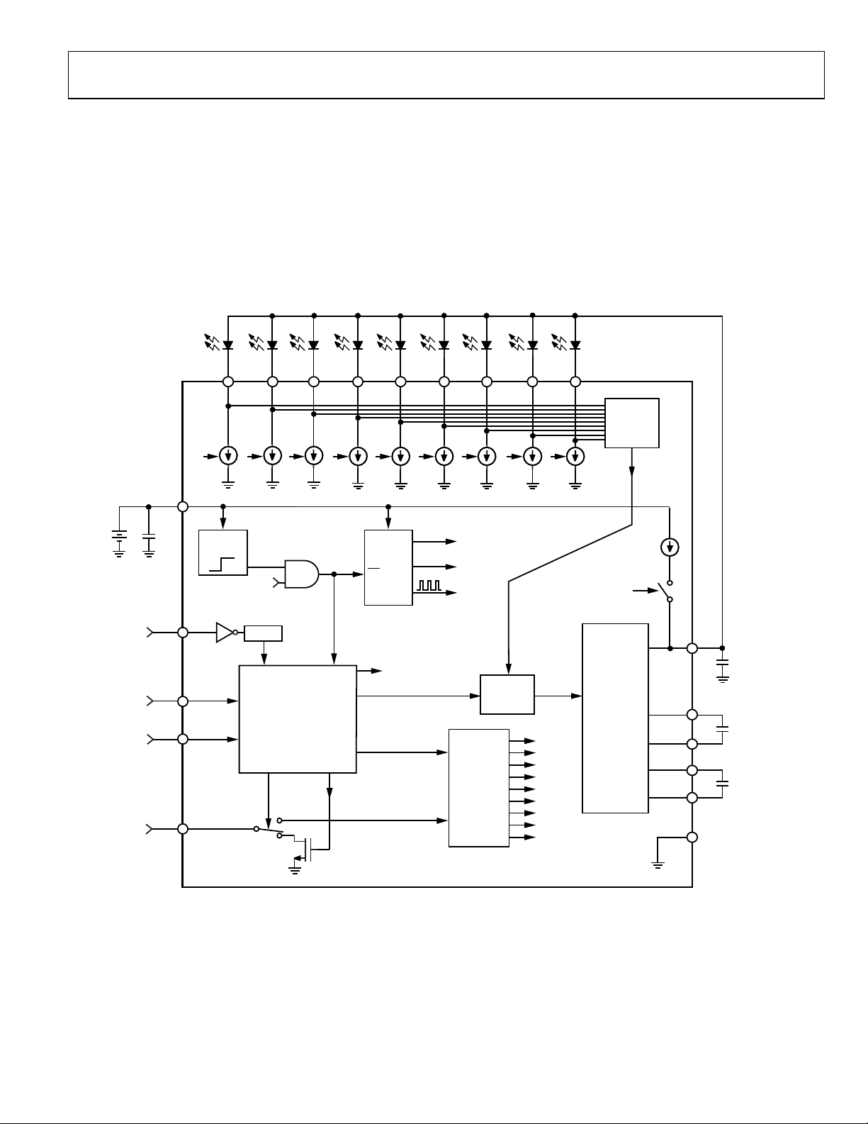
THEORY OF OPERATION
The ADP8866 combines a programmable backlight LED charge
pump driver with automatic blinking functions. Nine LED drivers
can be independently programmed at currents up to 25 mA.
The current level, fade time, and blinking rate can be programmed
once and executed autonomously on a loop. Separate fade-in
and fade-out times can be set for the backlight LEDs.
Driving all of this is a two capacitor charge pump with gains of
1×, 1.5×, and 2×. This setup is capable of driving a maximum
I
of 240 mA from a supply of 2.5 V to 5.5 V. A full suite of
OUT
safety features including short-circuit, overvoltage, and overtemperature protection allows easy implementation of a safe
and robust design. Additionally, input inrush currents are
limited via an integrated soft start combined with controlled
input to output isolation.
Figure 27. Detailed Block Diagram
Rev. 0 | Page 11 of 52
Page 12
ADP8866
09478-029
NOTES
1. V
DMAX
IS THE CAL CULATED GAI N DOWN TRANSITION P OINT.
WAIT
100µs (TYP)
MIN (V
D1:D9
) < V
HR(UP)
0
0
1
1
1
1
0
0
STARTUP:
CHARGE
V
IN
TO V
OUT
EXIT STANDBY
VOUT > V
OUT(START)
1
WAIT
100µs (TYP)
WAIT
100µs (TYP)
MIN (V
D1:D9
) < V
HR(UP)
MIN (V
D1:D9
) > V
DMAX
MIN (V
D1:D9
) < V
DMAX
G = 2
G = 1.5
EXIT
STARTUP
G = 1
STANDBY
0
POWER STAGE
Typical white LEDs require up to 4 V to drive them. Therefore,
some form of boosting is required to cover the typical Li Ion
battery voltage variation. The ADP8866 accomplishes this with
a high efficiency charge pump capable of producing a maximum
I
of 240 mA over the entire input voltage range of 2.5 V to
OUT
5.5 V. Charge pumps use the basic principle that a capacitor
stores charge based on the voltage applied to it, as shown in the
following equation:
Q = C × V (1)
By charging the capacitors in different configurations, the
charge and, therefore, the gain can be optimized to deliver the
voltage required to power the LEDs. Because a fixed charging
and discharging combination must be used, only certain
multiples of gain are available. The ADP8866 is capable of
automatically optimizing the gain (G) from 1×, 1.5×, and 2×.
These gains are accomplished with two capacitors and an
internal switching network.
In G = 1× mode, the switches are configured to pass VIN
directly to VOUT. In this mode, several switches are connected
in parallel to minimize the resistive drop from input to output.
In G = 1.5× and G = 2× modes, the switches alternatively charge
from the battery and discharge into the output. For G = 1.5×,
the capacitors are charged from VIN in series and are discharged to
VOUT in parallel. For G = 2×, the capacitors are charged from
VIN in parallel and are discharged to VOUT in parallel. In
certain fault modes, the switches are opened and the output is
physically isolated from the input.
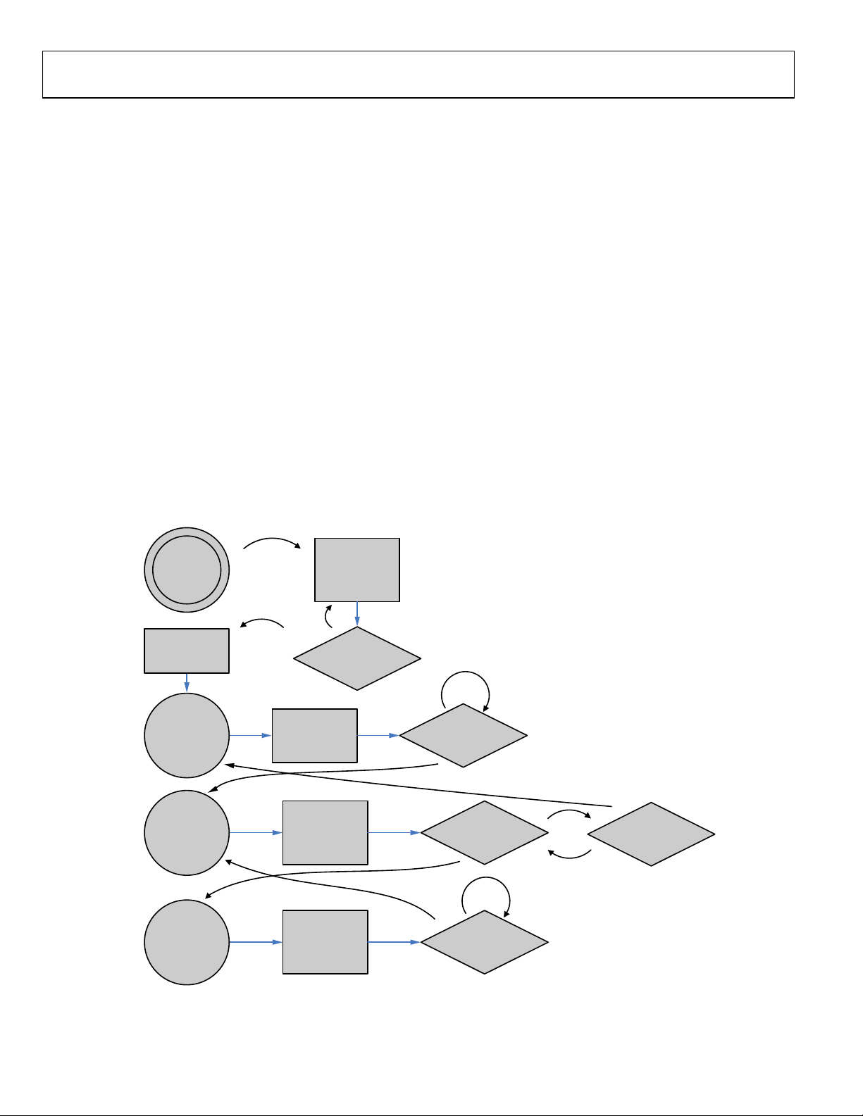
Automatic Gain Selection
Each LED that is driven requires a current source. The voltage
on this current source must be greater than a minimum headroom
voltage (V
) in Tabl e 1) to maintain accurate current
HR(MIN
regulation. The gain is automatically selected based on the
minimum voltage (V
) at all of the current sources. At startup,
DX
the device is placed into G = 1× mode and the output charges to
VIN. If any V
level is less than the required headroom, the
DX
gain is increased to the next step (G = 1.5×). A 100 μs delay is
allowed for the output to stabilize prior to the next gain
switching decision. If there remains insufficient current sink
headroom, the gain is increased again to 2×. Conversely, to
optimize efficiency, it is not desirable for the output voltage to be
too high. Therefore, the gain reduces when the headroom
voltage is too great. This point (labeled V
in Figure 28) is
DMAX
internally calculated to ensure that the lower gain still results in
ample headroom for all the current sinks. The entire cycle is
illustrated in Figure 28.
Figure 28. State Diagram for Automatic Gain Selection
Rev. 0 | Page 12 of 52
Page 13
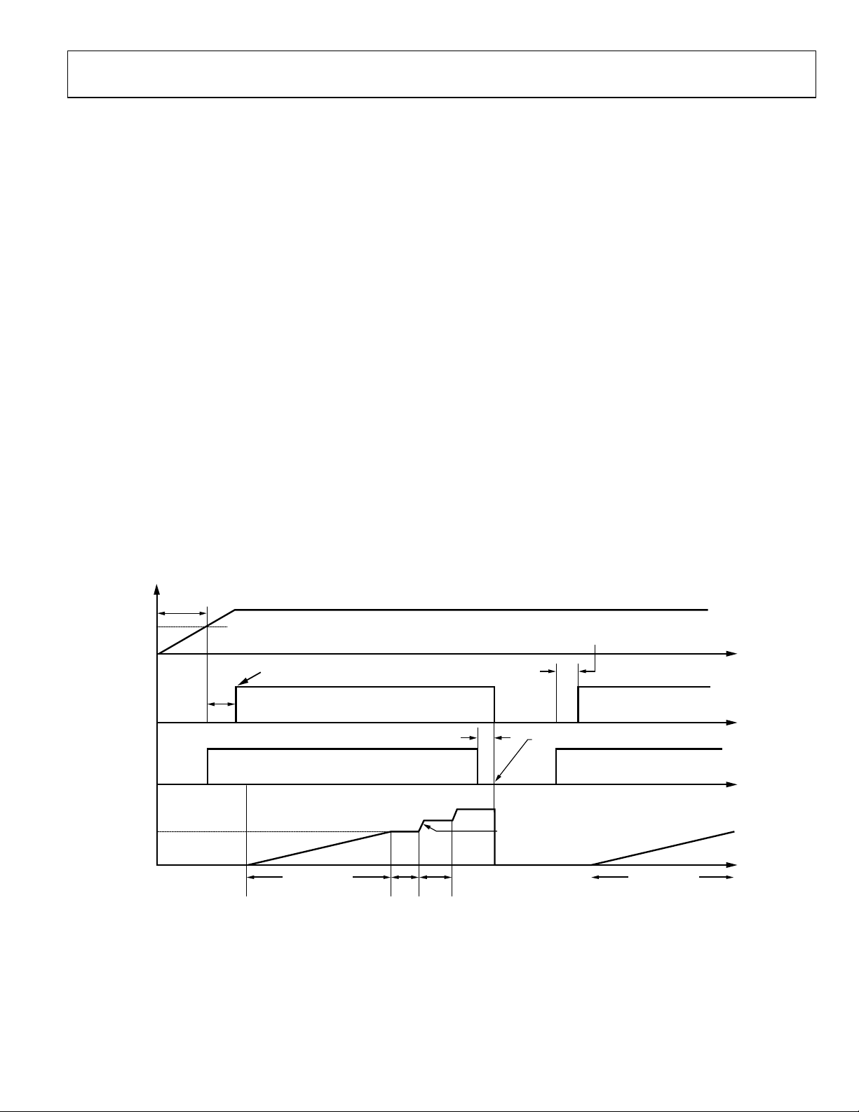
ADP8866
V
IN
nSTBY
nRST
V
OUT
V
IN
SHUTDOWN
VIN CROSSES ~ 2.0V AND TRIGGERS POWER ON RE S E T
BIT nSTBY IN REGISTER
MDCR GOES HIGH
nRST MUS T BE HIGH FOR 20µs (MAX )
BEFORE S E NDING I
2
C COMMANDS
nRST IS LOW, WHICH FORCES nSTBY LOW
AND RESETS ALL I
2
C REGISTERS
GAIN CHANGE S ONLY OCCUR WHEN NECESSARY
BUT HAVE A MI NIMUM TI M E BE FORE
CHANGING
~100µs DELAY BE TWEEN POWER UP AND
WHEN I
2
C COMMANDS CAN BE RE CE IVED
~7.0mA CHARGES
V
OUT
TO VIN LEVEL
25µs TO 100µ s NOISE F ILTER
1×
1.5×
2×
SOFT STARTSOFT START
10µs 100µs
09478-030
Note that the gain selection criteria applies only to active
current sources. If a current source has been deactivated
through an I
2
C command (that is, only five LEDs are used for
an application), the voltages on the deactivated current sources
are ignored.
Soft Start Feature
At startup (either from UVLO activation or fault/standby
recovery), the output is first charged by I
until it reaches about 92% of V
. This soft start feature reduces
IN
(7.0 mA typical)
SS
the inrush current that is otherwise present when the output
capacitance is initially charged to V
. When this point is
IN
reached, the controller enters 1× mode. If the output voltage is
not sufficient, the automatic gain selection determines the
optimal point as defined in the Automatic Gain Selection section.
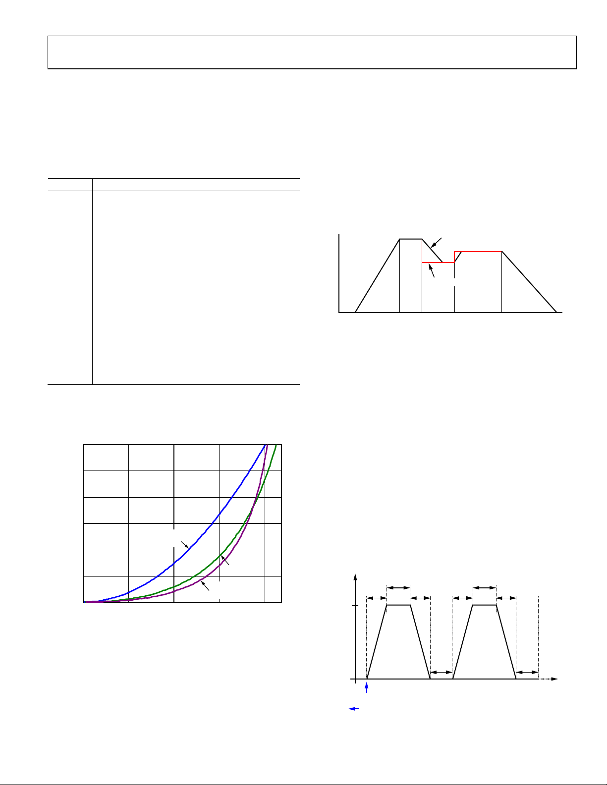
OPERATING MODES
There are four different operating modes: active, standby,
shutdown, and reset.
Active Mode
In active mode, all circuits are powered up and in a fully
operational state. This mode is entered when nSTBY (in
Register MDCR) is set to 1.
Standby Mode
Standby mode disables all circuitry except for the I2C receivers.
Current consumption is reduced to less than 1 μA. This mode is
entered when nSTBY is set to 0 or when the nRST pin is held
low for more than 100 μs (maximum). When standby is exited,
a soft start sequence is performed.
Shutdown Mode
Shutdown mode disables all circuitry, including the I2C receivers.
Shutdown occurs when V
When V
rises above V
IN
is below the undervoltage thresholds.
IN
(2.0 V typical), all registers are
IN(START)
reset and the part is placed into standby mode.
Reset Mode
In reset mode, all registers are set to their default values and the
part is placed into standby. There are two ways to reset the part:
power on reset (POR) and the nRST pin. POR is activated anytime that the part exits shutdown mode. After a POR sequence
is complete, the part automatically enters standby mode.
After startup, the part can be reset by pulling the nRST pin low.
As long as the nRST pin is low, the part is held in a standby state
2
but no I
C commands are acknowledged (all registers are kept
at their default values). After releasing the nRST pin, all registers
remain at their default values, and the part remains in standby;
however, the part does accept I
2
C commands.
The nRST pin has a 50 μs (typical) noise filter to prevent inadvertent activation of the reset function. The nRST pin must be
held low for this entire time to activate reset.
The operating modes function according to the timing diagram
in Figure 29.
Figure 29. Typical Timing Diagram
Rev. 0 | Page 13 of 52
Page 14
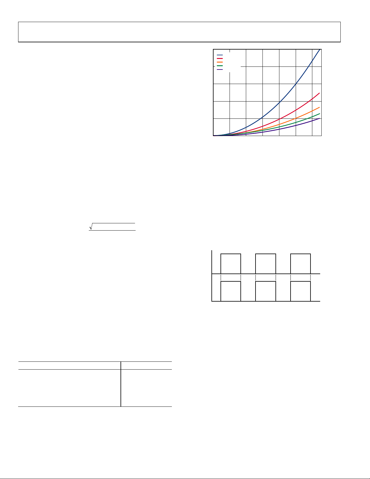
ADP8866
2
127
CurrentScaleFull
Codet(mA)LED_Curren
−
×=
25
20
15
10
5
0
0 12010080604020
OUTPUT CURRE NT (mA)
OUTPUT CURRE NT CODE (0 TO 127)
09478-031
25.00mA
12.50mA
8.33mA
6.25mA
5.00mA
09478-032
TIME
LED OUTP UT
CURRENT
nTNT PIN
(INPUT)
LED GROUPS
The nine LED channels can be separated into two groups: backlight
(BL) and independent sinks (ISC). The group select is done in
Register 0x09 and Register 0x0A, with the default being that all
LEDs are part of the backlight.
Each group has its own fade-in and fade-out times (Register
0x12 for backlight and Register 0x22 for ISCs). Each group also
has its own master enable located in Register 0x01. However,
this master enable is overwritten if any of the SCx_EN bits
(Register 0x1A and Register 0x1B) in a group are set high. This
allows complete independent control of each LED channel in
both groups.
OUTPUT CURRENT SETTINGS
The current setting is determined by a 7-bit code programmed
by the user into diode current control registers (Register 0x13
for the backlight and Register 0x23 to Register 0x2B for the
independent sinks). The 7-bit resolution allows the user to set
the backlight to one of 128 different levels between 0 mA and
25 mA. The ADP8866 implements a square law algorithm to
achieve a nonlinear relationship between input code and
backlight current. The LED output current (in milliamperes) is
determined by the following equation:
(2)
where:
Code is the input code programmed by the user.
Full-Scale Current is the maximum sink current allowed
per LED.
Figure 30. Output Code Effect on Various LEVEL_SET Ranges
The LEDs that receive this alternate current range are determined
by the DxLVL bits in Register 0x07 and Register 0x08.
PWM DIMMING
Setting the LEVEL_SET code to 111111 (binary) allows the
ADP8866 to dim its LEDs based on a PWM signal applied to the
nINT pin. The LED output current is pulse width modulated with
the signal applied to the nINT pin. The typical waveform and
timing are shown in Figure 29. Due to the inherent delays and
rise/fall times of this system, the best accuracy of the average output
current is obtained with PWM frequencies below 1 kHz.
OUTPUT CURRENT RANGE SELECTION
The default maximum current range of each sink of the
ADP8866 is 25.0 mA (typical). However, the ADP8866 also
allows the user to select an alternative maximum current range
to be applied to one or more LEDs. This alternate current range
still has 128 codes for its current setting. This provides
improved resolution when operating at reduced maximum
currents. One of up to 60 alternate current ranges can be
selected. An example of some of the available current ranges is
shown below. For the complete list, see Tab le 23.
Table 5. Example Current Range Options in Register 0x07
LEVEL_SET Code Range
000010 25.00 mA
001100 12.50 mA
010110 8.33 mA
100000 6.25 mA
101010 5.00 mA
In this mode, the nINT pin functions as an input. It no longer
provides notification of the INT_STAT register.
AUTOMATED FADE-IN AND FADE-OUT
The LED drivers are easily configured for automated fade-in
and fade-out. Sixteen fade-in and fade-out rates can be selected
via the I
0.0 sec to 1.75 sec (per full-scale current). Separate fade times are
assigned to the backlight LEDs and the ISC LEDs (see the LED
Groups section). The BLOFF_INT bit in Register 0x02 can be used
to flag the interrupt pin when an automated backlight fade-out has
occurred.
Rev. 0 | Page 14 of 52
Figure 31. PWM Input Waveform and Resultant LED Current
2
C interface. Fade-in and fade-out rates range from
Page 15
ADP8866
30
0
5
10
15
20
25
0 1.000.750.500.25
CURRENT (mA)
UNIT FADE TIME
SQUARE
CUBIC 11
CUBIC 10
09478-033
09478-034
BACKLIGHT CURRE NT
CABCFADE = 0 (DEFAULT)
BL EN = 1 BL EN = 0
TIME
FADE IN
COMPLETE
CHANGE
BL SETTING
CHANGE
BL SETTING
CABCFADE = 1
MAX
SCx_EN
SCx
CURRENT
FADE-IN FADE-OUT FADE-IN FADE-OUT
ON TIME ON TIME
OFF
TIME
OFF
TIME
SET BY USER
09478-035
The fade profile is based on the transfer law selected (square,
Cubic 10, or Cubic 11) and the delta between the actual current
and the target current. Smaller changes in current reduce the
fade time. For square law fades, the fade time is given by
Fade Time = Fade Rate × (Code/127) (4)
where the Fade Rate is shown in Tabl e 6.
Table 6. Available Fade-In and Fade-Out Times
Code Fade Rate (Seconds per 128 Codes)
0000 0.0
0001 0.05
0010 0.10
0011 0.15
0100 0.20
0101 0.25
0110 0.30
0111 0.35
1000 0.40
1001 0.45
1010 0.50
1011 0.75
1100 1.0
1101 1.25
1110 1.50
1111 1.75
The Cubic 10 and Cubic 11 laws also use the square backlight
currents in Equation 3; however, the time between each step is
varied to produce a steeper slope at higher currents and a
shallower slope at lighter currents (see Figure 32).
brightness control) operation, the BLMX register is updated as
often as 60 times per second. And the changes to BLMX must
be implemented as soon as possible. Therefore, the ADP8866
has a unique mode that allows the backlight to have very fast
changes after the initial ramp in and ramp out. This mode is
entered when CABCFADE in Register 0x10 is set high.
In this mode, the backlight fades in when BL_EN and nSTBY in
Register 0x01 are set high, and it fades out when BL_EN or
nSTBY is set low. However, after the fade-in is complete, any
changes to the BLMX register result in near instantaneous
changes to the backlight current. The situation is illustrated in
Figure 33.
Figure 33. Effect of the CABCFADE Bit
INDEPENDENT SINK CONTROL (ISC)
Each of the nine LEDs can be configured (in Register 0x10 and
Register 0x11) to operate as either part of the backlight or an
independent sink current (ISC). Each ISC can be enabled
independently and has its own current level. All ISCs share the
same fade-in rates, fade-out rates, and fade law.
The ISCs have additional timers to facilitate blinking functions.
A shared on timer (SCON), used in conjunction with the off
timers of each ISC (SC1OFF, SC2OFF, SC3OFF, SC4OFF,
SC5OFF, SC6OFF, and SC7OFF; see Register 0x1C through
Register 0x21) allow the LED current sinks to be configured in
various blinking modes. The on and off times are listed in the
Register Descriptions section. Blink mode is activated by setting
the off timers to any setting other than disabled.
Figure 32. Comparison of the Dimming Transfers Law 25 mA Scale Shown
CABC FADE DISABLE
The fade settings applied to the backlight in Register 0x12 are
also used when the BLMX (Register 0x13) current is changed.
This provides a smooth transition to new backlight current
levels.
Howe ver, in some modes of operation, this feature is not
desired. For example, during cABC (content adjustable
Figure 34. LEDx Blink Mode with Fading
Rev. 0 | Page 15 of 52
Page 16
ADP8866
09478-036
EN
SCFI
ISCx CURRENT
ISCx_HB CURRENT
SCFO SCFI SCFO
EVEN PULSE
OFFTIMERx
0 TO 126 SEC
SCON
0 TO 750ms
SCON_HB
0 TO 750ms
OFFTIMERx_HB
0 T
O 126 SEC
CURRENT (mA)
EVEN PULSE
ODD PULSE
ODD PULSE
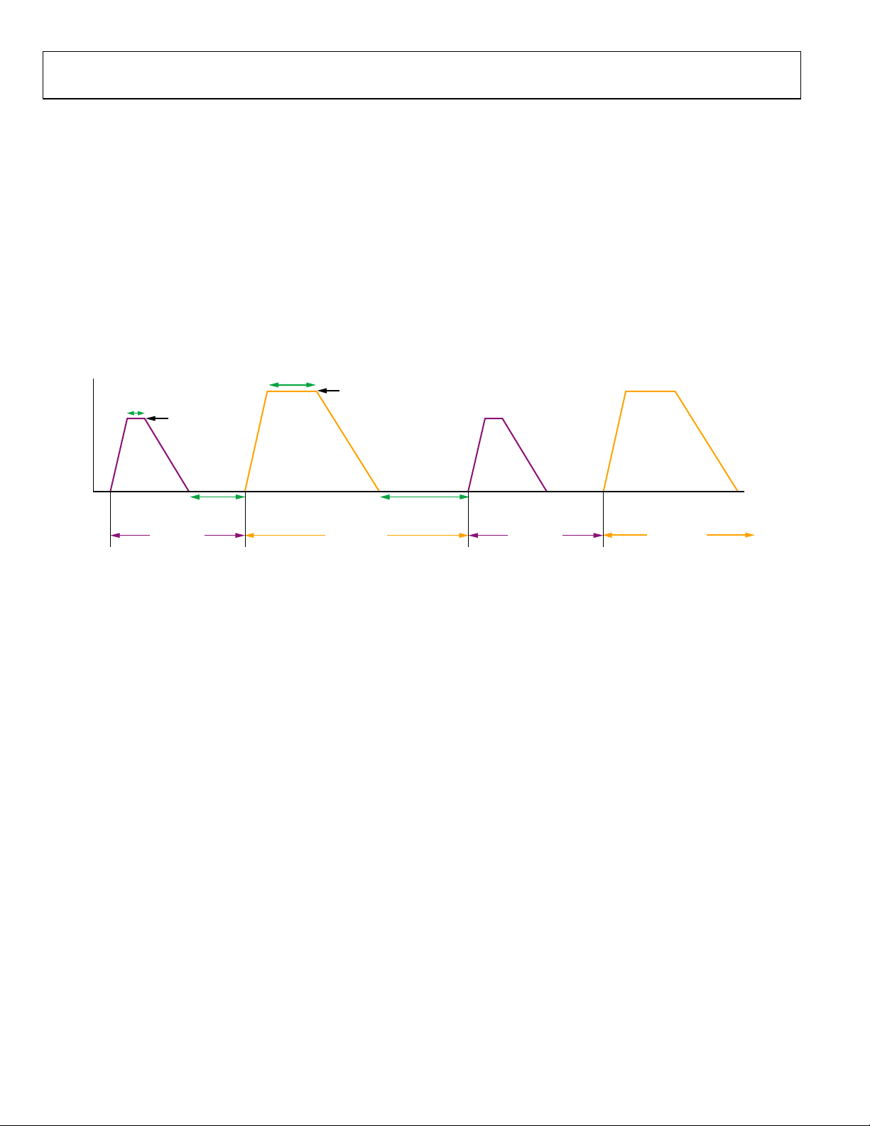
Program all fade-in and fade-out timers before enabling any of
the LED current sinks. If ISCx is on during a blink cycle and
SCx_EN in Register 0x1B is cleared, it turns off (or fades to off
if fade-out is enabled). If ISCx is off during a blink cycle and
SCx_EN is cleared, it stays off.
ADVANCED BLINKING CONTROLS
Diode D1 to Diode D5 have basic blinking controls, while
Channel D6 to Channel D9 have much more advanced
capabilities. These advanced features include
• Programmable delays: Register 0x3C to Register 0x3F set
the individual delays for D6 to D9. Delays are activated
when the individual diode is enabled. Delay times range
from 0 sec to 1.270 sec in 10 ms increments.
• Additional off time selections: D6 to D9 off times that
range from 0 sec to 12.5 sec in 100 ms increments (Register
0x1E to Register 0x21). The off times can also be set to off,
which turns the channel off at the completion of the blink
cycle. The LED turns on again when the enable signal is
toggled.
• Heartbeat mode: This mode allows a double pulse to be
issued in a fully automated and customizable loop. Register
0x2C through Register 0x35 control the heartbeat effect.
Up to four channels (D6 to D9) can be configured to
operate in the heartbeat mode. The approximate shape of
the heartbeat is shown in Figure 35:
Figure 35. Customizable Heartbeat Pulse
Rev. 0 | Page 16 of 52
Page 17

ADP8866
SHORT-CIRCUIT PROTECTION (SCP) MODE
The ADP8866 can protect against short circuits on the output
). Short-circuit protection (SCP) is activated at the point
(V
OUT
when V
< 55% of VIN. Note that this SCP sensing is disabled
OUT
during startup and restart attempts (fault recovery). SCP
sensing is reenabled 4 ms (typical) after activation. During a
short-circuit fault, the device enters a low current consumption
state and an interrupt flag is set. The device can be restarted at
any time after receiving a short-circuit fault by simply rewriting
nSTBY = 1 in Register 0x01. It then repeats another complete
soft start sequence. Note that the value of the output
capacitance (C
reach approximately 55% (typical) of V
(typical) time. If C
) should be small enough to allow V
OUT
within the 4 ms
IN
is too large, the device inadvertently
OUT
OUT
to
enters short-circuit protection.
OVERVOLTAGE PROTECTION (OVP)
Overvoltage protection is implemented on the VOUT pin.
There are two types of overvoltage events: normal (no fault) and
abnormal.
Normal (No Fault) Overvoltage
In this case, the VOUT pin voltage approaches V
typical) during normal operation. This is not caused by a fault
or load change but is simply a consequence of the input voltage
times the gain reaching the clamped output voltage V
prevent this, the ADP8866 detects when the output voltage rises
to V
. It then increases the effective R
OUT(REG)
of the gain stage
OUT
to reduce the voltage that is delivered. This effectively regulates
V
to V
OUT
system can have on regulating V
; however, there is a limit to the effect that this
OUT(REG)
. It is designed only for
OUT
normal operation and is not intended to protect against faults or
sudden load changes. During this mode, no interrupt is set, and
the operation is transparent to the LEDs and overall application.
OUT(REG)
(4.9 V
OUT(REG)
. To
The automatic gain selection equations take into account the
additional drop within R
to maintain optimum efficiency.
OUT
Abnormal (Fault/Sudden Load Change) Overvoltage
Because of the open loop behavior of the charge pump, as well
as how the gain transitions are computed, a sudden load change
or fault can abnormally force V
beyond 6 V. If the event
OUT
happens slowly enough, the system first tries to regulate the
output to 4.9 V as in a normal overvoltage scenario. However, if
this is not sufficient, or if the event happens too quickly, the
ADP8866 enters overvoltage protection mode when V
OUT
exceeds the OVP threshold (typically 5.7 V). In this mode, only
the charge pump is disabled to prevent V
from rising too
OUT
high. The current sources and all other device functionality
remain intact. When the output voltage falls by about 500 mV
(to 5.2 V typical), the charge pump resumes operation. If the
fault or load step recurs, the process may repeat. An interrupt
flag is set at each OVP instance.
THERMAL SHUTDOWN (TSD)/OVERTEMPERATURE PROTECTION
If the die temperature of the ADP8866 rises above a safety limit
(150°C typical), the controllers enter TSD protection mode. In
this mode, most of the internal functions are shut down, the
part enters standby, and the TSD_INT interrupt is set (see
Register 0x02). When the die temperature decreases below
~130°C, the part is allowed to be restarted. To restart the part,
simply remove it from standby. No interrupt is generated when
the die temperature falls below 130°C. However, if the software
clears the pending TSD_INT interrupt and the temperature
remains above 130°C, another interrupt is generated.
The complete state machine for these faults (SCP, OVP, and
TSD) is shown in Figure 36.
Rev. 0 | Page 17 of 52
Page 18

ADP8866
WAIT
100µs (TYP)
G = 2
G = 1.5
0
0
1
1
1
1
0
V
OUT
> V
OUT(REG)
TRY TO
REGULATE
VOUT TO
V
OUT(REG)
VOUT > V
OVP
OVP FAULT
VOUT < V
OVP
–
V
OVP
(HYS)
0
1
0
1
1
0
VOUT > V
OVP
OVP FAULT
0
1
0
1
1
0
EXIT
STARTUP
G = 1
STANDBY
1
0
VOUT < V
OUT(SC)
0
SCP FAULT
EXIT ST ANDBY
STARTUP:
CHARGE
V
IN
TO V
OUT
V
OUT
> V
OUT(START)
DIE TEMP > TSD
0
TSD FAULT
DIE TEMP <
TSD – TSD
(HYS)
MIN (V
D1:D9
)
< V
HR(UP)
MIN (V
D1:D9
)
< V
HR(UP)
MIN (V
D1:D9
)
> V
DMAX
MIN (V
D1:D9
)
> V
DMAX
1
0
EXIT ST ANDBY
WAIT
100µs (TYP)
WAIT
100µs (TYP)
VOUT < V
OVP
–
V
OVP (HYS)
V
OUT
> V
OUT(REG)
TRY TO
REGULATE
VOUT TO
V
OUT(REG)
NOTES
1. V
DMAX
IS THE CALCULATED GAIN DOWN TRANSI TION POINT.
09478-037
1
0
Figure 36. Fault State Machine
Rev. 0 | Page 18 of 52
Page 19

ADP8866
BL_EN = 1 BL_EN = 0
BLOFF_INT SET
BACKLIGHT CURRE NT
MAX
FADE-IN
OFF-TO-MAX
FADE-OUT
MAX-TO-OFF
09478-038
SCx_EN = 1
SCxOFF
ISCOFF_INT SET
ISCOFF_INT SET
ISC CURRENT
FADE-IN FADE-OUT
SCON
09478-039
INTERRUPTS
There are four interrupt sources available on the ADP8866.
• Independent sink off: when all independent sinks that are
assigned with the DxOFFINT bits high in Register 0x04
and Register 0x05 have faded to off, this interrupt
(ISCOFF_INT, Register 0x02) is set.
• Backlight off: at the end of each automated backlight fade-
out, this interrupt (BLOFF_INT, Register 0x02) is set.
• Overvoltage protection: OVP_INT (see Register 0x02) is
generated when the output voltage exceeds 5.7 V (typical).
• Thermal shutdown circuit: an interrupt (TSD_INT,
Register 0x02) is generated when entering
overtemperature protection.
• Short-circuit detection: SHORT_INT (see Register 0x02) is
generated when the device enters short-circuit protection
mode.
The interrupt (if any) that appears on the nINT pin is
determined by the bits mapped in Register INT_EN, 0x03. To
clear an interrupt, write a 1 to the interrupt in the INT_STAT
register, 0x02, or reset the part.
BACKLIGHT OFF INTERRUPT
The backlight off interrupt (BLOFF_INT) is set when the
backlight completes a fade-out. This feature is useful to
synchronize the backlight turn off with the LCD display driver.
Figure 37. Backlight Off Interrupt Timing Diagram
INDEPENDENT SINK OFF INTERRUPT
The independent sink off interrupt (ISCOFF_INT) is generated
when all the independent sinks assigned in Register 0x04 and
Register 0x05 have faded to off. This can happen during a
blinking profile (where SCxOFF does not equal disabled) or
when an ISC is disabled. Note that even with fade-out set to 0,
an ISCOFF_INT is still set.
Figure 38. Independent Sink Off Interrupt Timing Diagram
Rev. 0 | Page 19 of 52
Page 20

ADP8866
09478-040
V
DX
C
OUT
G × V
IN
R
OUT
V
OUT
I
OUT
APPLICATIONS INFORMATION
The ADP8866 allows the charge pump to operate efficiently
with a minimum of external components. Specifically, the user
must select an input capacitor (C
and two charge pump fly capacitors (C1 and C2). C
), output capacitor (C
IN
OUT
should be
IN
),
1 μF or greater. The value must be high enough to produce a
stable input voltage signal at the minimum input voltage and
maximum output load. A 1 μF capacitor for C
is recommended.
OUT
Larger values are permissible, but care must be exercised to ensure
that VOUT charges above 55% (typical) of VIN within 4 ms
(typical). See the Short-Circuit Protection (SCP) Mode section
for more detail.
For best practice, it is recommended that the two charge pump
fly capacitors be 1 μF; larger values are not recommended and
smaller values may reduce the ability of the charge pump to
deliver maximum current. For optimal efficiency, the charge
pump fly capacitors should have low equivalent series resistance
(ESR). Low ESR X5R or X7R capacitors are recommended for
all four components. Minimum voltage ratings should adhere to
the guidelines in Tabl e 7:
Table 7. Capacitor Stress in Each Charge Pump Gain State
Capacitor Gain = 1× Gain = 1.5× Gain = 2×
CIN (Input Capacitor) VIN VIN VIN
C
(Output
OUT
Capacitor)
C1 (Charge Pump
Capacitor)
C2 (Charge Pump
Capacitor)
VIN VIN × 1.5
(Max of 5.5 V)
None VIN ÷ 2 VIN
None VIN ÷ 2 VIN
VIN × 2.0
(Max of 5.5 V)
Any color LED can be used provided that the Vf (forward
voltage) is less than 4.3 V. However, using lower Vf LEDs
reduces the input power consumption by allowing the charge
pump to operate at lower gain states.
The equivalent model for a charge pump is shown in Figure 39.
Figure 39. Charge Pump Equivalent Circuit Model
The input voltage is multiplied by the gain (G) and delivered to
the output through an effective charge pump resistance (R
The output current flows through R
and produces an IR
OUT
OUT
).
drop, which yields
The R
= G × VIN − I
V
OUT
term is a combination of the R
OUT
OUT
× R
(G) (6)
OUT
resistance for the
DSON
switches used in the charge pump and a small resistance that
accounts for the effective dynamic charge pump resistance. The
R
level changes based upon the gain (the configuration of the
OUT
switches). Typical R
values are given in Table 1 and Figure 14
OUT
and Figure 16.
V
is also equal to the largest Vf of the LEDs used plus the
OUT
voltage drop across the regulating current source. This gives
V
OUT
= Vf
+ VDX (7)
(MAX)
Combining Equation 6 and Equation 7 gives
V
= (Vf
IN
(MAX)
+ VDX + I
OUT
× R
(G))/G (8)
OUT
This equation is useful for calculating approximate bounds for
the charge pump design.
Determining the Transition Point of the Charge Pump
Consider the following design example where:
Vf
= 3.7 V
(MAX)
= 140 mA (7 LEDs at 20 mA each)
I
OUT
(G = 1.5×) = 3 Ω (obtained from Figure 12)
R
OUT
At the point of a gain transition, V
typical value of V
as 0.2 V. Therefore, the input voltage
HR(UP)
DX
= V
. Tabl e 1 gives the
HR(UP)
level when the gain transitions from 1.5× to 2× is
V
= (3.7 V + 0.2 V + 140 mA × 3 Ω)/1.5 = 2.88 V
IN
LAYOUT GUIDELINES
• For optimal noise immunity, place the C
capacitors as close to their respective pins as possible.
These capacitors should share a short ground trace. If the
LEDs are a significant distance from the VOUT pin,
another capacitor on VOUT, placed closer to the LEDs, is
advisable.
• For optimal efficiency, place the charge pump fly capacitors
as close to the part as possible.
• The ground pin should be connected at the ground for the
input and output capacitors. The LFCSP exposed pad must
be soldered at the board to the GND pin.
• Unused diode pins [D1:D9] can be connected to ground or
VOUT or remain floating. However, the unused diode
current sinks must be removed from the charge pump gain
calculation by setting the appropriate DxPWR bits high in
Register 0x09 and Register 0x0A.
• If the interrupt pin (nINT) is not used, connect it to
ground or leave it floating. Never connect it to a voltage
supply, except through a ≥1 kΩ series resistor.
• The ADP8866 has an integrated noise filter on the nRST
pin. Under normal conditions, it is not necessary to filter
the reset line. However, if exposed to an unusually noisy
signal, it is beneficial to add a small RC filter or bypass
capacitor on this pin. If the nRST pin is not used, it must
be pulled well above the V
level (see Table 1). Do not
IH(MAX)
allow the nRST pin to float.
and C
IN
OUT
Rev. 0 | Page 20 of 52
Page 21

ADP8866
ST
ACK REGISTER ADDRESS
ACK REGISTER VALUE
ACK
0 1 0 0 1 1 1
START
DEVICE ID
FOR WRITE
OPERATION
ST
B7 B0 B7 B0 B7 B0
STOP
WRITE = 0
FROM POTHOOK
FROM POTHOOK
FROM POTHOOK
SELECT REGISTER TO WRITE 8-BIT VALUE TO WRITE IN THE
ADDRESSED REGISTER
SLAVE TO MASTER
MASTER TO SLAVE
09478-041
R/W
SLAVE TO MASTER
MASTER TO SLAVE
ST
R/W
ACK REGISTER ADDRESS
ACK ACK REGISTER VALUE
ACK0 1 0 0 1 1 1
START
DEVICE ID
FOR WRITE
OPERATION
ST
B7 B0 B7 B0 B7 B0
STOP
WRITE = 0
FROM POTHOOK
FROM POTHOOK
FROM MASTER
SELECT REGISTER TO WRITE 8-BIT VALUE TO WRITE IN THE
ADDRESSED REGISTER
RS 0 1 0 0 1 1 1
REPEATED START
DEVICE ID
FOR READ
OPERATION
B7 B0
READ = 1
09478-042
R/W
FROM POTHOOK
I2C PROGRAMMING AND DIGITAL CONTROL
The ADP8866 provides full software programmability to
facilitate its adoption in various product architectures. The I
2
C
address is 0100111x (x = 0 during write, x = 1 during read).
Therefore, the write address is 0x4E, and the read address is
0x4F.
Notes on the general behavior of registers:
• All registers are set to default values on reset or in case of a
UVLO event.
• All registers are read/write unless otherwise specified
• Unused bits are read-as-zero.
Tabl e 8 through Tab l e 103 provide register and bit descriptions.
The reset value for all bits in the bit map tables is all 0s, except
in Tab l e 9 (see Tabl e 9 for its unique reset value). Wherever the
acronym N/A appears in the tables, it means not applicable.
Figure 40. I
2
C Write Sequence
Figure 41. I
2
C Read Sequence
Rev. 0 | Page 21 of 52
Page 22

ADP8866
REGISTER DESCRIPTIONS
Table 8. Register Map
Address Name Bit 7 Bit 6 Bit 5 Bit 4 Bit 3 Bit 2 Bit 1 Bit 0
0x00 MFDVID Manufacture ID Device ID
0x01 MDCR Reserved INT_CFG NSTBY ALT_GSEL GDWN_DIS SIS_EN Reserved BL_EN
0x02 INT_STAT Reserved ISCOFF_INT BLOFF_INT SHORT_INT TSD_INT OVP_INT Reserved Reserved
0x03 INT_EN Reserved ISCOFF_IEN BLOFF_IEN SHORT_IEN TSD_IEN OVP_IEN Reserved Reserved
0x04 ISCOFF_SEL1 Reserved D9OFFINT
0x05 ISCOFF_SEL2 D8OFFINT D7OFFINT D6OFFINT D5OFFINT D4OFFINT D3OFFINT D2OFFINT D1OFFINT
0x06 GAIN_SEL Reserved 1.5X_LIMIT G_FORCE
0x07 LVL_SEL1 Reserved D9LVL LEVEL_SET
0x08 LVL_SEL2 D8LVL D7LVL D6LVL D5LVL D4LVL D3LVL D2LVL D1LVL
0x09 PWR_SEL1 Reserved D9PWR
0x0A PWR_SEL2 D8PWR D7PWR D6PWR D5PWR D4PWR D3PWR D2PWR D1PWR
0x0B to 0x0F Reserved Reserved
0x10 CFGR Reserved D9SEL CABCFADE BL_LAW Reserved
0x11 BLSEL D8SEL D7SEL D6SEL D5SEL D4SEL D3SEL D2SEL D1SEL
0x12 BLFR BL_FO BL_FI
0x13 BLMX Reserved BL_MC
0x14 to 0x19 Reserved Reserved
0x1A ISCC1 Reserved SC9_EN SC_LAW
0x1B ISCC2 SC8_EN SC7_EN SC6_EN SC5_EN SC4_EN SC3_EN SC2_EN SC1_EN
0x1C ISCT1 SCON Reserved SC5OFF
0x1D ISCT2 SC4OFF SC3OFF SC2OFF SC1OFF
0x1E OFFTIMER6 Reserved SC6OFF
0x1F OFFTIMER7 Reserved SC7OFF
0x20 OFFTIMER8 Reserved SC8OFF
0x21 OFFTIMER9 Reserved SC9OFF
0x22 ISCF SCFO SCFI
0x23 ISC1 Reserved SCD1
0x24 ISC2 Reserved SCD2
0x25 ISC3 Reserved SCD3
0x26 ISC4 Reserved SCD4
0x27 ISC5 Reserved SCD5
0x28 ISC6 Reserved SCD6
0x29 ISC7 Reserved SCD7
0x2A ISC8 Reserved SCD8
0x2B ISC9 Reserved SCD9
0x2C HB_SEL Reserved D9HB_EN D8HB_EN D7HB_EN D6HB_EN
0x2D ISC6_HB Reserved SCD6_HB
0x2E ISC7_HB Reserved SCD7_HB
0x2F ISC8_HB Reserved SCD8_HB
0x30 ISC9_HB Reserved SCD9_HB
0x31 OFFTIMER6_HB Reserved SC6OFF_HB
0x32 OFFTIMER7_HB Reserved SC7OFF_HB
0x33 OFFTIMER8_HB Reserved SC8OFF_HB
0x34 OFFTIMER9_HB Reserved SC9OFF_HB
0x35 ISCT_HB Reserved SCON_HB
0x36 to 0x3B Reserved Reserved
0x3C DELAY6 Reserved DELAY6
0x3D DELAY7 Reserved DELAY7
0x3E DELAY8 Reserved DELAY8
0x3F DELAY9 Reserved DELAY9
Rev. 0 | Page 22 of 52
Page 23

ADP8866
Manufacturer and Device ID (MFDVID)—Register 0x00
Multiple device revisions are tracked by the device ID field. This is a read-only register.
Table 9. MFDVID Manufacturer and Device ID Bit Map
Bit 7 Bit 6 Bit 5 Bit 4 Bit 3 Bit 2 Bit 1 Bit 0
Manufacture ID Device ID
0 1 0 1 0 0 1 1
Mode Control Register (MDCR)—Register 0x01
Table 10. MDCR Bit Map
Bit 7 Bit 6 Bit 5 Bit 4 Bit 3 Bit 2 Bit 1 Bit 0
Reserved INT_CFG NSTBY ALT_GSEL GDWN_DIS SIS_EN Reserved BL_EN
Table 11.
Bit Name Bit No. Description
N/A 7 Reserved.
INT_CFG 6 Interrupt configuration.
1 = processor interrupt deasserts for 50 μs and reasserts with pending events.
0 = processor interrupt remains asserted if the host tries to clear the interrupt while there is a pending event.
NSTBY 5 1 = device is in normal mode.
0 = device is in standby, only I2C is enabled.
ALT_GSEL 4 1 = charge pump gain is automatically set to 1× every time that the BLMX (Register 0x13) is written to.
0 = writing to BLMX (Register 13) has no unique effect on the charge pump gain.
GDWN_DIS 3
SIS_EN 2 Master enable for independent sinks.
N/A 1 Reserved.
BL_EN 0 Master enable for backlight sinks.
1 = the charge pump does not switch down in gain until all LEDs are off. The charge pump switches up in gain
as needed. This feature is useful if the ADP8866 charge pump is used to drive an external load.
0 = the charge pump automatically switches up and down in gain. This provides optimal efficiency but is not
suitable for driving external loads (other than those connected to the ADP8866 diode drivers).
1 = enables all LED current sinks designated as independent sinks. This bit has no effect if any of the SCx_EN
bits that are part of the independent sinks group in Register 0x1A and Register 0x1B are set.
0 = disables all sinks designated as independent sinks. This bit has no effect if any of the SCx_EN bits that are
part of the independent sinks group in Register 0x1A and Register 0x1B are set.
1 = enables all LED current sinks designated as backlight.
0 = disables all sinks designated as backlight.
Rev. 0 | Page 23 of 52
Page 24

ADP8866
Interrupt Status Register (INT_STAT)—Register 0x02
Table 12. INT_STAT Bit Map
Bit 7 Bit 6 Bit 5 Bit 4 Bit 3 Bit 2 Bit 1 Bit 0
Reserved ISCOFF_INT BLOFF_INT SHORT_INT TSD_INT OVP_INT Reserved
Table 13.
Bit Name Bit No. Description1
N/A 7 Reserved.
ISCOFF_INT 6 Independent sink off.
1 = indicates that the controller has ramped all the independent sinks designated in Register 0x04 and
Register 0x05 to off.
0 = the controller has not ramped all designated independent sinks to off.
BLOFF_INT 5 Backlight off.
1 = indicates that the controller has faded the backlight sinks to off.
0 = the controller has not completed fading the backlight sinks to off.
SHORT_INT 4 Short-circuit error.
1 = a short-circuit or overload condition on VOUT or current sinks was detected.
0 = no short-circuit or overload condition was detected.
TSD_INT 3 Thermal shutdown.
1 = device temperature is too high and has been shut down.
0 = no overtemperature condition was detected.
OVP_INT 2 Overvoltage interrupt.
1 = charge-pump output voltage has exceeded V
0 = charge-pump output voltage has not exceeded V
N/A [1:0] Reserved.
1
Interrupt bits are cleared by writing a 1 to the flag; writing a 0 or reading the flag has no effect.
Interrupt Enable (INT_EN)—Register 0x03
OVP
.
.
OVP
Table 14. INT_EN Bit Map
Bit 7 Bit 6 Bit 5 Bit 4 Bit 3 Bit 2 Bit 1 Bit 0
Reserved ISCOFF_IEN BLOFF_IEN SHORT_IEN TSD_IEN OVP_IEN Reserved
Table 15.
Bit Name Bit No. Description
N/A 7 Reserved.
ISCOFF_IEN 6 Automated ISC off indicator.
1 = the automated independent sink off indicator is enabled.
0 = the automated independent sink off indicator is disabled.
BLOFF_IEN 5 Automated backlight off indicator.
1 = the automated backlight off indicator is enabled.
0 = the automated backlight off indicator is disabled.
When this bit is set, an INT is generated anytime that a backlight fade-out is over. This occurs after an automated
fade-out or after the completion of a backlight dimming profile. This is useful to synchronize the complete turn off
for the backlights with other devices in the application.
SHORT_IEN 4
1 = the short-circuit interrupt is enabled.
0 = the short-circuit interrupt is disabled (SHORT_INT flag is still asserted).
TSD_IEN 3
1 = the thermal shutdown interrupt is enabled.
0 = the thermal shutdown interrupt is disabled (TSD_INT flag is still asserted).
Short-circuit interrupt enabled. When the SHORT_INT status bit is set after an error condition, an interrupt is raised
to the host if the SHORT_IEN flag is enabled.
Thermal shutdown interrupt enabled. When the TSD_INT status bit is set after an error condition, an interrupt is
raised to the host if the TSD_IEN flag is enabled.
Rev. 0 | Page 24 of 52
Page 25

ADP8866
Bit Name Bit No. Description
OVP_IEN 2
1 = the overvoltage interrupt is enabled.
0 = the overvoltage interrupt is disabled (OVP_INT flag is still asserted).
N/A [1:0] Reserved.
Independent Sink Interrupt Selection 1 (ISCOFF_SEL1)—Register 0x04
Table 16. ISCOFF_SEL1 Bit Map
Bit 7 Bit 6 Bit 5 Bit 4 Bit 3 Bit 2 Bit 1 Bit 0
Table 17.
Bit Name Bit No. Description
N/A [7:1] Reserved.
D9OFFINT 0 Include Diode 9 in the ISCOFF_INT flag.
0 = Diode 9 is not in the group which triggers an ISCOFF_INT when all diodes in that group are off.
Independent Sink Interrupt Selection 2 (ISCOFF_SEL2)—Register 0x05
Overvoltage interrupt enabled. When the OVP_INT status bit is set after an error condition, an interrupt is raised to
the host if the OVP_IEN flag is enabled.
Reserved D9OFFINT
1 = Diode 9 is in the group which triggers an ISCOFF_INT. When Diode 9 and all other LEDs with
DxOFFINT are set high and go from on to off, ISCOFF_INT is set.
Table 18. ISCOFF_SEL2 Bit Map
Bit 7 Bit 6 Bit 5 Bit 4 Bit 3 Bit 2 Bit 1 Bit 0
D8OFFINT D7OFFINT D6OFFINT D5OFFINT D4OFFINT D3OFFINT D2OFFINT D1OFFINT
Table 19.
Bit Name Bit No. Description
D8OFFINT 7 Include Diode 8 in the ISCOFF_INT flag.
0 = Diode 8 is not in the group that triggers an ISCOFF_INT when all diodes in that group are off.
D7OFFINT 6 Include Diode 7 in the ISCOFF_INT flag.
0 = Diode 7 is not in the group that triggers an ISCOFF_INT when all diodes in that group are off.
D6OFFINT 5 Include Diode 6 in the ISCOFF_INT flag.
0 = Diode 6 is not in the group that triggers an ISCOFF_INT when all diodes in that group are off.
D5OFFINT 4 Include Diode 5 in the ISCOFF_INT flag.
0 = Diode 5 is not in the group that triggers an ISCOFF_INT when all diodes in that group are off.
D4OFFINT 3 Include Diode 4 in the ISCOFF_INT flag.
0 = Diode 4 is not in the group that triggers an ISCOFF_INT when all diodes in that group are off.
D3OFFINT 2 Include Diode 3 in the ISCOFF_INT flag.
0 = Diode 3 is not in the group that triggers an ISCOFF_INT when all diodes in that group are off.
1 = Diode 8 is in the group that triggers an ISCOFF_INT. When Diode 8 and all other LEDs with
DxOFFINT are set high and goes from on to off, ISCOFF_INT is set.
1 = Diode 7 is in the group that triggers an ISCOFF_INT. When Diode 7 and all other LEDs with
DxOFFINT are set high and goes from on to off, ISCOFF_INT is set.
1 = Diode 6 is in the group that triggers an ISCOFF_INT. When Diode 6 and all other LEDs with
DxOFFINT are set high and goes from on to off, ISCOFF_INT is set.
1 = Diode 5 is in the group that triggers an ISCOFF_INT. When Diode 5 and all other LEDs with
DxOFFINT are set high and goes from on to off, ISCOFF_INT is set.
1 = Diode 4 is in the group that triggers an ISCOFF_INT. When Diode 4 and all other LEDs with
DxOFFINT are set high and goes from on to off, ISCOFF_INT is set.
1 = Diode 3 is in the group that triggers an ISCOFF_INT. When Diode 3 and all other LEDs with
DxOFFINT are set high and goes from on to off, ISCOFF_INT is set.
Rev. 0 | Page 25 of 52
Page 26

ADP8866
Bit Name Bit No. Description
D2OFFINT 1 Include Diode 2 in the ISCOFF_INT flag.
0 = Diode 2 is not in the group that triggers an ISCOFF_INT when all diodes in that group are off.
D1OFFINT 0 Include Diode 1 in the ISCOFF_INT flag.
0 = Diode 1 is not in the group that triggers an ISCOFF_INT when all diodes in that group are off.
Charge Pump Gain Selection (GAIN_SEL)—Register 0x06
Table 20. GAIN_SEL Bit Map
Bit 7 Bit 6 Bit 5 Bit 4 Bit 3 Bit 2 Bit 1 Bit 0
Table 21.
Bit Name Bit No. Description
N/A 7:3 Reserved.
1.5X_LIMIT 2 1 = gain is allowed to transition up from 1× to 1.5×. The gain is never allowed to enter 2× mode.
0 = gain is allowed to transition up from 1× to 1.5× to 2× as needed.
G_FORCE [1:0] Selects desired gain state.
00 = auto gain select.
01 = gain is locked into 1× mode.
10 = gain is locked into 1.5× mode.
11 = gain is locked into 2× mode (if 1.5X_LIMIT = 1, gain is locked into 1.5×)
Output Level Selection 1 (LVL_SEL1)—Register 0x07
1 = Diode 2 is in the group that triggers an ISCOFF_INT. When Diode 2 and all other LEDs with
DxOFFINT are set high and goes from on to off, ISCOFF_INT is set.
1 = Diode 1 is in the group that triggers an ISCOFF_INT. When Diode 1 and all other LEDs with
DxOFFINT are set high and goes from on to off, ISCOFF_INT is set.
Reserved 1.5X_LIMIT G_FORCE
Table 22. LVL_SEL1 Bit Map
Bit 7 Bit 6 Bit 5 Bit 4 Bit 3 Bit 2 Bit 1 Bit 0
Reserved D9LVL LEVEL_SET
Table 23.
Bit Name Bit No. Description
N/A 7 Reserved.
D9LVL 6 Diode 9 level select.
1 = control with the LEVEL_SET bits.
0 = normal mode (25 mA full-scale current).
LEVEL_SET [5:0] Output level selection. Sets the mode of operation for all DxLVL bits that are set high.
000000 0.8 25 mA ÷ N = 31.3 mA
000001 0.9 25 mA ÷ N = 27.8 mA
000010 1.0 25 mA ÷ N = 25.0 mA
000011 1.1 25 mA ÷ N = 22.7 mA
… … …
111110 7.0 25 mA ÷ N = 3.6 mA
111111 1.0
Code N Maximum Current Range
PWM current. In this mode, the INT pin functions as a PWM input and directly drives
the selected outputs.
Rev. 0 | Page 26 of 52
Page 27

ADP8866
Table 24.
Code N Maximum Current Range (mA) Code N Maximum Current Range (mA)
000000 0.8 31.3 100000 4 6.25
000001 0.9 27.8 100001 4.1 6.10
000010 1 25.0 100010 4.2 5.95
000011 1.1 22.7 100011 4.3 5.81
000100 1.2 20.8 100100 4.4 5.68
000101 1.3 19.2 100101 4.5 5.56
000110 1.4 17.9 100110 4.6 5.43
000111 1.5 16.7 100111 4.7 5.32
001000 1.6 15.6 101000 4.8 5.21
001001 1.7 14.7 101001 4.9 5.10
001010 1.8 13.9 101010 5 5.00
001011 1.9 13.2 101011 5.1 4.90
001100 2 12.5 101100 5.2 4.81
001101 2.1 11.9 101101 5.3 4.72
001110 2.2 11.4 101110 5.4 4.63
001111 2.3 10.9 101111 5.5 4.55
010000 2.4 10.4 110000 5.6 4.46
010001 2.5 10.0 110001 5.7 4.39
010010 2.6 9.62 110010 5.8 4.31
010011 2.7 9.26 110011 5.9 4.24
010100 2.8 8.93 110100 6 4.17
010101 2.9 8.62 110101 6.1 4.10
010110 3 8.33 110110 6.2 4.03
010111 3.1 8.06 110111 6.3 3.97
011000 3.2 7.81 111000 6.4 3.91
011001 3.3 7.58 111001 6.5 3.85
011010 3.4 7.35 111010 6.6 3.79
011011 3.5 7.14 111011 6.7 3.73
011100 3.6 6.94 111100 6.8 3.68
011101 3.7 6.76 111101 6.9 3.62
011110 3.8 6.58 111110 7.0 3.57
011111 3.9 6.41 111111 1.0 PWM current
Output Level Selection 2 (LVL_SEL2)—Register 0x08
Table 25. LVL_SEL2 Bit Map
Bit 7 Bit 6 Bit 5 Bit 4 Bit 3 Bit 2 Bit 1 Bit 0
D8LVL D7 LVL D6LVL D5LVL D4LVL D 3LVL D2LVL D1 LVL
Table 26.
Bit Name Bit No. Description
D8LVL 7 Diode 8 level select.
1 = control with the LEVEL_SET bits.
0 = normal mode (25 mA full-scale current).
D7LVL 6 Diode 7 level select.
1 = control with the LEVEL_SET bits.
0 = normal mode (25 mA full-scale current).
D6LVL 5 Diode 6 level select.
1 = control with the LEVEL_SET bits.
0 = normal mode (25 mA full-scale current).
Rev. 0 | Page 27 of 52
Page 28

ADP8866
Bit Name Bit No. Description
D5LVL 4 Diode 5 level select.
1 = control with the LEVEL_SET bits.
0 = normal mode (25 mA full-scale current).
D4LVL 3 Diode 4 level select.
1 = control with the LEVEL_SET bits.
0 = normal mode (25 mA full-scale current).
D3LVL 2 Diode 3 level select.
1 = control with the LEVEL_SET bits.
0 = normal mode (25 mA full-scale current).
D2LVL 1 Diode 2 level select.
1 = control with the LEVEL_SET bits.
0 = normal mode (25 mA full-scale current).
D1LVL 0 Diode 1 level select.
1 = control with the LEVEL_SET bits.
0 = normal mode (25 mA full-scale current).
LED Power Source Selection 1 (PWR_SEL1)—Register 0x09
Table 27. PWR_SEL1 Bit Map
Bit 7 Bit 6 Bit 5 Bit 4 Bit 3 Bit 2 Bit 1 Bit 0
Reserved D9PWR
Table 28.
Bit Name Bit No. Description
N/A [7:1] Reserved.
D9PWR 0 Diode 9 LED power source select.
1 = the LED is powered from the battery or other power source.
0 = the LED is powered from the charge pump.
LED Power Source Selection 2 (PWR_SEL2)—Register 0x0A
Table 29. PWR_SEL2 Bit Map
Bit 7 Bit 6 Bit 5 Bit 4 Bit 3 Bit 2 Bit 1 Bit 0
D8PWR D7PWR D6PWR D5PWR D4PWR D3PWR D2PWR D1PWR
Table 30.
Bit Name Bit No. Description
D8PWR 7 Diode 8 LED power source select.
1 = the LED is powered from the battery or other power source.
0 = the LED is powered from the charge pump.
D7PWR 6 Diode 7 LED power source select.
1 = the LED is powered from the battery or other power source.
0 = the LED is powered from the charge pump.
D6PWR 5 Diode 6 LED power source select.
1 = the LED is powered from the battery or other power source.
0 = the LED is powered from the charge pump.
D5PWR 4 Diode 5 LED power source select.
1 = the LED is powered from the battery or other power source.
0 = the LED is powered from the charge pump.
D4PWR 3 Diode 4 LED power source select.
1 = the LED is powered from the battery or other power source.
0 = the LED is powered from the charge pump.
Rev. 0 | Page 28 of 52
Page 29

ADP8866
Bit Name Bit No. Description
D3PWR 2 Diode 3 LED power source select.
1 = the LED is powered from the battery or other power source.
0 = the LED is powered from the charge pump.
D2PWR 1 Diode 2 LED power source select.
1 = the LED is powered from the battery or other power source.
0 = the LED is powered from the charge pump.
D1PWR 0 Diode 1 LED power source select.
1 = the LED is powered from the battery or other power source.
0 = the LED is powered from the charge pump.
BACKLIGHT REGISTER DESCRIPTIONS
Configuration Register (CFGR)—Register 0x10
Table 31. CFGR Bit Map
Bit 7 Bit 6 Bit 5 Bit 4 Bit 3 Bit 2 Bit 1 Bit 0
Reserved D9SEL CABCFADE BL_LAW Reserved
Table 32.
Bit Name Bit No. Description
N/A [7:5] Reserved.
D9SEL 4 Diode 9 backlight select.
1 = selects LED9 as part of the independent sinks group.
0 = selects LED9 as part of the backlight group.
CABCFADE 3
BL_LAW [2:1] Backlight transfer law.
N/A 0 Reserved.
Selects how the backlight current responds to changes in its I
in is complete.
1 = any changes to the backlight current setting (Register 0x13) result in a near instant transition to the new current
level. This is useful when rapid changes to the backlight current are required, such as during cABC control.
0 = any changes to the backlight current setting (Register 0x13) result in a fade to the new current level. The fade
time is determined by the fade rate (set in Register 0x12) and the delta between the old and new current level.
00 = square law DAC, linear time steps.
01 = square law DAC, linear time steps.
10 = square law DAC, nonlinear time steps (Cubic 10).
11 = square law DAC, nonlinear time steps (Cubic 11).
Backlight Select (BLSEL)—Register 0x11
2
C setpoint after the backlight is enabled and the fade-
Table 33. BLSEL Bit Map
Bit 7 Bit 6 Bit 5 Bit 4 Bit 3 Bit 2 Bit 1 Bit 0
D8SEL D7SEL D6SEL D5SEL D4SEL D3SEL D2SEL D1SEL
Table 34.
Bit Name Bit No. Description
D8SEL 7 Diode 8 backlight select.
1 = selects LED8 as part of the independent sinks group.
0 = selects LED8 as part of the backlight group.
D7SEL 6 Diode 7 backlight select.
1 = selects LED7 as part of the independent sinks group.
0 = selects LED7 as part of the backlight group.
D6SEL 5 Diode 6 backlight select.
1 = selects LED6 as part of the independent sinks group.
0 = selects LED6 as part of the backlight group.
Rev. 0 | Page 29 of 52
Page 30

ADP8866
Bit Name Bit No. Description
D5SEL 4 Diode 5 backlight select.
1 = selects LED5 as part of the independent sinks group.
0 = selects LED5 as part of the backlight group.
D4SEL 3 Diode 4 backlight select.
1 = selects LED4 as part of the independent sinks group.
0 = selects LED4 as part of the backlight group.
D3SEL 2 Diode 3 backlight select.
1 = selects LED3 as part of the independent sinks group.
0 = selects LED3 as part of the backlight group.
D2SEL 1 Diode 2 backlight select.
1 = selects LED2 as part of the independent sinks group.
0 = selects LED2 as part of the backlight group.
D1SEL 0 Diode 1 backlight select.
1 = selects LED1 as part of the independent sinks group.
0 = selects LED1 as part of the backlight group.
Backlight Fade (BLFR)—Register 0x12
Table 35. BLFR Bit Map
Bit 7 Bit 6 Bit 5 Bit 4 Bit 3 Bit 2 Bit 1 Bit 0
BL_FO BL_FI
Table 36.
Bit Name Bit No. Description
BL_FO [7:4]
0000 = 0.0 sec (fade-out disabled).
0001 = 0.05 sec.
0010 = 0.10 sec.
0011 = 0.15 sec.
0100 = 0.20 sec.
0101 = 0.25 sec.
0110 = 0.30 sec.
0111 = 0.35 sec.
1000 = 0.40 sec.
1001 = 0.45 sec.
1010 = 0.50 sec.
1011 = 0.75 sec.
1100 = 1.00 sec.
1101 = 1.25 sec.
1110 = 1.50 sec.
1111 = 1.75 sec.
BL_FI [3:0]
0000 = 0.0 sec (fade-in disabled).
0001 = 0.05 sec.
0010 = 0.10 sec.
0011 = 0.15 sec.
…
1111 = 1.75 sec.
Backlight fade-out rate. The backlight fades from its current value to the off value. The times listed for BL_FO
are for a full-scale fade-out. Fades between closer current values reduce the fade time. See the Automated
Fade-in and Fade-Out section for more information.
Backlight fade-in rate. The backlight fades from 0 to its programmed value when the backlight is turned on.
The times listed for BL_FI are for a full-scale fade-in. Fades between closer current values reduce the fade time.
See the Automated Fade-in and Fade -Out section for more information.
Rev. 0 | Page 30 of 52
Page 31

ADP8866
Backlight Maximum Current Register (BLMX)—Register 0x13
Table 37. BLMX Bit Map
Bit 7 Bit 6 Bit 5 Bit 4 Bit 3 Bit 2 Bit 1 Bit 0
Reserved BL_MC
Table 38.
Bit Name Bit No. Description
N/A 7 Reserved.
BL_MC [6:0]
Backlight maximum current. The backlight maximum current can be set according to the square law function. All
values scale with the setting of LEVEL_SET. See Table 39 for a complete list of values.
DAC
Code
Current (mA)
(Full Scale =
25 mA)
LEVEL_SET =
000010
Current (mA)
(Full Scale =
12.5 mA)
LEVEL_SET =
001100
Current (mA)
(Full Scale =
8.25 mA)
LEVEL_SET =
010110
Current (mA)
(Full Scale =
6.25 mA)
LEVEL_SET =
100000
Current (mA)
(Full Scale =
5.0 mA)
LEVEL_SET =
101010
0x00 0.0 0.0 0.0 0.0 0.0
0x01 0.0016 0.0008 0.0005 0.0004 0.0003
0x02 0.0062 0.0031 0.0021 0.0016 0.0012
0x03 0.014 0.0070 0.0047 0.0035 0.0028
… … … … … …
0x7F 25.0 12.5 8.33 6.25 5.0
Table 39. Diode Output Currents per DAC Code
DAC Code
Current (mA)
(Full Scale = 25 mA)
LEVEL_SET = 000010
Current (mA)
(Full Scale = 12.5 mA)
LEVEL_SET = 001100
Current (mA)
(Full Scale = 8.25 mA)
LEVEL_SET = 010110
Current (mA)
(Full Scale = 6.25 mA)
LEVEL_SET = 100000
Current (mA)
(Full Scale = 5.0 mA)
LEVEL_SET = 101010
0x00 0.0 0.0 0.0 0.0 0.0
0x01 0.0016 0.0008 0.0005 0.0004 0.0003
0x02 0.0062 0.0031 0.0021 0.0016 0.0012
0x03 0.014 0.0070 0.0047 0.0035 0.0028
0x04 0.025 0.012 0.0083 0.0062 0.0050
0x05 0.039 0.019 0.013 0.010 0.0078
0x06 0.056 0.028 0.019 0.014 0.011
0x07 0.076 0.038 0.025 0.019 0.015
0x08 0.099 0.050 0.033 0.025 0.020
0x09 0.126 0.063 0.042 0.031 0.025
0x0A 0.155 0.078 0.052 0.039 0.031
0x0B 0.188 0.094 0.063 0.047 0.038
0x0C 0.223 0.112 0.074 0.056 0.045
0x0D 0.262 0.131 0.087 0.065 0.052
0x0E 0.304 0.152 0.101 0.076 0.061
0x0F 0.349 0.174 0.116 0.087 0.070
0x10 0.397 0.198 0.132 0.099 0.079
0x11 0.448 0.224 0.149 0.112 0.090
0x12 0.502 0.251 0.167 0.126 0.100
0x13 0.560 0.280 0.187 0.140 0.112
0x14 0.620 0.310 0.207 0.155 0.124
0x15 0.684 0.342 0.228 0.171 0.137
0x16 0.750 0.375 0.250 0.188 0.150
0x17 0.820 0.410 0.273 0.205 0.164
0x18 0.893 0.446 0.298 0.223 0.179
0x19 0.969 0.484 0.323 0.242 0.194
0x1A 1.05 0.524 0.349 0.262 0.210
0x1B 1.13 0.565 0.377 0.282 0.226
0x1C 1.22 0.608 0.405 0.304 0.243
Rev. 0 | Page 31 of 52
Page 32

ADP8866
Current (mA)
(Full Scale = 25 mA)
DAC Code
0x1D 1.30 0.652 0.435 0.326 0.261
0x1E 1.40 0.698 0.465 0.349 0.279
0x1F 1.49 0.745 0.497 0.372 0.298
0x20 1.59 0.794 0.529 0.397 0.317
0x21 1.69 0.844 0.563 0.422 0.338
0x22 1.79 0.896 0.597 0.448 0.358
0x23 1.90 0.949 0.633 0.475 0.380
0x24 2.01 1.00 0.670 0.502 0.402
0x25 2.12 1.06 0.707 0.530 0.424
0x26 2.24 1.12 0.746 0.560 0.448
0x27 2.36 1.18 0.786 0.589 0.472
0x28 2.48 1.24 0.827 0.620 0.496
0x29 2.61 1.30 0.869 0.651 0.521
0x2A 2.73 1.37 0.911 0.684 0.547
0x2B 2.87 1.43 0.955 0.716 0.573
0x2C 3.00 1.50 1.00 0.750 0.600
0x2D 3.14 1.57 1.05 0.785 0.628
0x2E 3.28 1.64 1.09 0.820 0.656
0x2F 3.42 1.71 1.14 0.856 0.685
0x30 3.57 1.79 1.19 0.893 0.714
0x31 3.72 1.86 1.24 0.930 0.744
0x32 3.88 1.94 1.29 0.969 0.775
0x33 4.03 2.02 1.34 1.01 0.806
0x34 4.19 2.10 1.40 1.05 0.838
0x35 4.35 2.18 1.45 1.09 0.871
0x36 4.52 2.26 1.51 1.13 0.904
0x37 4.69 2.34 1.56 1.17 0.938
0x38 4.86 2.43 1.62 1.22 0.972
0x39 5.04 2.52 1.68 1.26 1.01
0x3A 5.21 2.61 1.74 1.30 1.04
0x3B 5.40 2.70 1.80 1.35 1.08
0x3C 5.58 2.79 1.86 1.40 1.12
0x3D 5.77 2.88 1.92 1.44 1.15
0x3E 5.96 2.98 1.99 1.49 1.19
0x3F 6.15 3.08 2.05 1.54 1.23
0x40 6.35 3.17 2.12 1.59 1.27
0x41 6.55 3.27 2.18 1.64 1.31
0x42 6.75 3.38 2.25 1.69 1.35
0x43 6.96 3.48 2.32 1.74 1.39
0x44 7.17 3.58 2.39 1.79 1.43
0x45 7.38 3.69 2.46 1.84 1.48
0x46 7.60 3.80 2.53 1.90 1.52
0x47 7.81 3.91 2.60 1.95 1.56
0x48 8.04 4.02 2.68 2.01 1.61
0x49 8.26 4.13 2.75 2.06 1.65
0x4A 8.49 4.24 2.83 2.12 1.70
0x4B 8.72 4.36 2.91 2.18 1.74
0x4C 8.95 4.48 2.98 2.24 1.79
0x4D 9.19 4.59 3.06 2.30 1.84
0x4E 9.43 4.72 3.14 2.36 1.89
0x4F 9.67 4.84 3.22 2.42 1.93
LEVEL_SET = 000010
Current (mA)
(Full Scale = 12.5 mA)
LEVEL_SET = 001100
Current (mA)
(Full Scale = 8.25 mA)
LEVEL_SET = 010110
Current (mA)
(Full Scale = 6.25 mA)
LEVEL_SET = 100000
Current (mA)
(Full Scale = 5.0 mA)
LEVEL_SET = 101010
Rev. 0 | Page 32 of 52
Page 33

ADP8866
Current (mA)
(Full Scale = 25 mA)
DAC Code
0x50 9.92 4.96 3.31 2.48 1.98
0x51 10.2 5.08 3.39 2.54 2.03
0x52 10.4 5.21 3.47 2.61 2.08
0x53 10.7 5.34 3.56 2.67 2.14
0x54 10.9 5.47 3.65 2.73 2.19
0x55 11.2 5.60 3.73 2.80 2.24
0x56 11.5 5.73 3.82 2.87 2.29
0x57 11.7 5.87 3.91 2.93 2.35
0x58 12.0 6.00 4.00 3.00 2.40
0x59 12.3 6.14 4.09 3.07 2.46
0x5A 12.6 6.28 4.19 3.14 2.51
0x5B 12.8 6.42 4.28 3.21 2.57
0x5C 13.1 6.56 4.37 3.28 2.62
0x5D 13.4 6.70 4.47 3.35 2.68
0x5E 13.7 6.85 4.57 3.42 2.74
0x5F 14.0 6.99 4.66 3.50 2.80
0x60 14.3 7.14 4.76 3.57 2.86
0x61 14.6 7.29 4.86 3.65 2.92
0x62 14.9 7.44 4.96 3.72 2.98
0x63 15.2 7.60 5.06 3.80 3.04
0x64 15.5 7.75 5.17 3.88 3.10
0x65 15.8 7.91 5.27 3.95 3.16
0x66 16.1 8.06 5.38 4.03 3.23
0x67 16.4 8.22 5.48 4.11 3.29
0x68 16.8 8.38 5.59 4.19 3.35
0x69 17.1 8.54 5.70 4.27 3.42
0x6A 17.4 8.71 5.81 4.35 3.48
0x6B 17.7 8.87 5.92 4.44 3.55
0x6C 18.1 9.04 6.03 4.52 3.62
0x6D 18.4 9.21 6.14 4.60 3.68
0x6E 18.8 9.38 6.25 4.69 3.75
0x6F 19.1 9.55 6.37 4.77 3.82
0x70 19.4 9.72 6.48 4.86 3.89
0x71 19.8 9.90 6.60 4.95 3.96
0x72 20.1 10.1 6.71 5.04 4.03
0x73 20.5 10.2 6.83 5.12 4.10
0x74 20.9 10.4 6.95 5.21 4.17
0x75 21.2 10.6 7.07 5.30 4.24
0x76 21.6 10.8 7.19 5.40 4.32
0x77 21.9 11.0 7.32 5.49 4.39
0x78 22.3 11.2 7.44 5.58 4.46
0x79 22.7 11.3 7.56 5.67 4.54
0x7A 23.1 11.5 7.69 5.77 4.61
0x7B 23.4 11.7 7.82 5.86 4.69
0x7C 23.8 11.9 7.94 5.96 4.77
0x7D 24.2 12.1 8.07 6.05 4.84
0x7E 24.6 12.3 8.20 6.15 4.92
0x7F 25.0 12.5 8.33 6.25 5.00
LEVEL_SET = 000010
Current (mA)
(Full Scale = 12.5 mA)
LEVEL_SET = 001100
Current (mA)
(Full Scale = 8.25 mA)
LEVEL_SET = 010110
Current (mA)
(Full Scale = 6.25 mA)
LEVEL_SET = 100000
Current (mA)
(Full Scale = 5.0 mA)
LEVEL_SET = 101010
Rev. 0 | Page 33 of 52
Page 34

ADP8866
INDEPENDENT SINK REGISTER DESCRIPTIONS
Independent Sink Current Control Register 1 (ISCC1)—Register 0x1A
Table 40. ISCLAW Bit Map
Bit 7 Bit 6 Bit 5 Bit 4 Bit 3 Bit 2 Bit 1 Bit 0
Reserved SC9_EN SC_LAW
Table 41.
Bit Name Bit No. Description
N/A 7:3 Reserved.
SC9_EN 2 This enable acts on LED9.
1 = SC9 is turned on.
0 = SC9 is turned off.
SC_LAW 1:0 SC fade transfer law.
00 = square law DAC, linear time steps.
01 = square law DAC, linear time steps.
10 = square law DAC, nonlinear time steps (Cubic 10).
11 = square law DAC, nonlinear time steps (Cubic 11).
Independent Sink Current Control Register 2 (ISCC2)—Register 0x1B
Table 42. ISCC Bit Map
Bit 7 Bit 6 Bit 5 Bit 4 Bit 3 Bit 2 Bit 1 Bit 0
SC8_EN SC7_EN SC6_EN SC5_EN SC4_EN SC3_EN SC2_EN SC1_EN
Table 43.
Bit Name Bit No. Description
SC8_EN 7 This enable acts on LED8.
1 = SC8 is turned on.
0 = SC8 is turned off.
SC7_EN 6 This enable acts on LED7.
1 = SC7 is turned on.
0 = SC7 is turned off.
SC6_EN 5 This enable acts on LED6.
1 = SC6 is turned on.
0 = SC6 is turned off.
SC5_EN 4 This enable acts on LED5.
1 = SC5 is turned on.
0 = SC5 is turned off.
SC4_EN 3 This enable acts on LED4.
1 = SC4 is turned on.
0 = SC4 is turned off.
SC3_EN 2 This enable acts on LED3.
1 = SC3 is turned on.
0 = SC3 is turned off.
SC2_EN 1 This enable acts on LED2.
1 = SC2 is turned on.
0 = SC2 is turned off.
SC1_EN 0 This enable acts on LED1.
1 = SC1 is turned on.
0 = SC1 is turned off.
Rev. 0 | Page 34 of 52
Page 35

ADP8866
Independent Sink Current Time (ISCT1)—Register 0x1C
Table 44. ISCT1 Bit Map
Bit 7 Bit 6 Bit 5 Bit 4 Bit 3 Bit 2 Bit 1 Bit 0
SCON
Table 45.
Bit Name Bit No. Description
SCON [7:4]
SC on time. If the SCxOFF time is not disabled, then when the independent current sink is enabled (Register 0x1A
and Register 0x1B), it remains on for the on time selected (per the following list) and then turns off.
0000 = 0.00 sec1.
0001 = 0.05 sec.
0010 = 0.10 sec.
0011 = 0.15 sec.
0100 = 0.20 sec.
0101 = 0.25 sec.
0110 = 0.30 sec.
0111 = 0.35 sec.
1000 = 0.40 sec.
1001 = 0.45 sec.
1010 = 0.50 sec.
1011 = 0.55 sec.
1100 = 0.60 sec.
1101 = 0.65 sec.
1110 = 0.70 sec.
1111 = 0.75 sec.
N/A [3:2] Reserved.
SC5OFF [1:0]
SC5 off time. When the SC off time is disabled, the SC remains on while enabled. When the SC off time is set to any
other value, the ISC turns off for the off time (per the following listed times) and then turns on according to the
SCON setting.
00 = off time disabled2.
01 = 0.6 sec.
10 = 1.2 sec.
11 = 1.8 sec.
1
If SCON is set to 0 sec, then after the ISC completes a ramp up, it immediately starts to ramp back down again (if SCxOFF is not disabled). SCON should not be set to 0 if
the fade-in time is also 0 seconds.
2
An independent sink remains on continuously when it is enabled and SCxOFF is disabled.
Independent Sink Current Time (ISCT2)—Register 0x1D
Reserved
SC5OFF
Table 46. ISCT2 Bit Map
Bit 7 Bit 6 Bit 5 Bit 4 Bit 3 Bit 2 Bit 1 Bit 0
SC4OFF SC3OFF SC2OFF SC1OFF
Rev. 0 | Page 35 of 52
Page 36

ADP8866
Table 47.
Designation Bit Description1
SC4OFF [7:6]
SC3OFF [5:4]
SC2OFF [3:2]
SC1OFF [1:0]
1
An independent sink remains on continuously when it is enabled and SCxOFF is 00 (disabled).
Independent Sink 6 Off Timer (OFFTIMER6)—Register 0x1E
SC4 off time. When the SC off time is disabled, the SC remains on while enabled. When the SC off time is set to any
other value, the ISC turns off for the off time (per the following listed times) and then turns on according to the
SCON setting.
00 = off time disabled.
01 = 0.6 sec.
10 = 1.2 sec.
11 = 1.8 sec.
SC3 off time. When the SC off time is disabled, the SC remains on while enabled. When the SC off time is set to any
other value, the ISC turns off for the off time (per the following listed times) and then turns on according to the
SCON setting.
00 = off time disabled.
01 = 0.6 sec.
10 = 1.2 sec.
11 = 1.8 sec.
SC2 off time. When the SC off time is disabled, the SC remains on while enabled. When the SC off time is set to any
other value, the ISC turns off for the off time (per the following listed times) and then turns on according to the
SCON setting.
00 = off time disabled.
01 = 0.6 sec.
10 = 1.2 sec.
11 = 1.8 sec.
SC1 off time. When the SC off time is disabled, the SC remains on while enabled. When the SC off time is set to any
other value, the ISC turns off for the off time (per the following listed times) and then turns on according to the
SCON setting.
00 = off time disabled.
01 = 0.6 sec.
10 = 1.2 sec.
11 = 1.8 sec.
Table 48. OFFTIMER6 Bit Map
Bit 7 Bit 6 Bit 5 Bit 4 Bit 3 Bit 2 Bit 1 Bit 0
Reserved SC6OFF
Table 49.
Bit Name Bit No. Description
N/A 7 Reserved.
SC6OFF [6:0]
SC6 off time. When the SC off time is disabled, the SC remains on while enabled. When the SC off time is set to
any other value, the ISC turns off for the off time (per the following listed times) and then turns on according to
the SCON setting.
0000 = disabled1.
0000001 = 0.0 sec2.
0000010 = 0.1 sec.
0000011 = 0.2 sec.
…
1111110 = 12.5 sec.
1111111 = off3.
1
An independent sink remains on continuously when it is enabled and SCxOFF is 00 (disabled).
2
Setting SCxOFF to 0 seconds is not recommended if the SCFO fade-out time is also set to 0 seconds.
3
Setting SCxOFF to off causes the LED to be held off indefinitely. This is useful for setting up a blink sequence that runs once and then goes to off.
Rev. 0 | Page 36 of 52
Page 37

ADP8866
Independent Sink 7 Off Timer (OFFTIMER7)—Register 0x1F
Table 50. OFFTIMER7 Bit Map
Bit 7 Bit 6 Bit 5 Bit 4 Bit 3 Bit 2 Bit 1 Bit 0
Reserved SC7OFF
Table 51.
Bit Name Bit No. Description
N/A 7 Reserved.
SC7OFF [6:0]
1
An independent sink remains on continuously when it is enabled and SCxOFF is 00 (disabled).
2
Setting SCxOFF to 0 seconds is not recommended if the SCFO fade-out time is also set to 0 seconds.
3
Setting SCxOFF to off causes the LED to be held off indefinitely. This is useful for setting up a blink sequence that runs once and then goes to off.
Independent Sink 8 Off Timer (OFFTIMER8)—Register 0x20
SC7 off time. When the SC off time is disabled, the SC remains on while enabled. When the SC off time is set to
any other value, the ISC turns off for the off time (per the following listed times) and then turns on according to
the SCON setting.
0000 = disabled1.
0000001 = 0.0 sec2.
0000010 = 0.1 sec.
0000011 = 0.2 sec.
…
1111110 = 12.5 sec.
1111111 = off3.
Table 52. OFFTIMER8 Bit Map
Bit 7 Bit 6 Bit 5 Bit 4 Bit 3 Bit 2 Bit 1 Bit 0
Reserved SC8OFF
Table 53.
Bit Name Bit No. Description
N/A 7 Reserved
SC8OFF [6:0]
SC8 off time. When the SC off time is disabled, the SC remains on while enabled. When the SC off time is set to
any other value, the ISC turns off for the off time (per the following listed times) and then turns on according to
the SCON setting.
0000 = disabled1.
0000001 = 0.0 sec2.
0000010 = 0.1 sec.
0000011 = 0.2 sec.
…
1111110 = 12.5 sec.
1111111 = off3.
1
An independent sink remains on continuously when it is enabled and SCxOFF is 00 (disabled).
2
Setting SCxOFF to 0 seconds is not recommended if the SCFO fade-out time is also set to 0 seconds.
3
Setting SCxOFF to off causes the LED to be held off indefinitely. This is useful for setting up a blink sequence that runs once and then goes to off.
Rev. 0 | Page 37 of 52
Page 38

ADP8866
Independent Sink 9 Off Timer (OFFTIMER9)—Register 0x21
Table 54. OFFTIMER9 Bit Map
Bit 7 Bit 6 Bit 5 Bit 4 Bit 3 Bit 2 Bit 1 Bit 0
Reserved SC9OFF
Table 55.
Bit Name Bit No. Description
N/A 7 Reserved.
SC9OFF [6:0]
1
An independent sink remains on continuously when it is enabled and SCxOFF is 00 (disabled).
2
Setting SCxOFF to 0 seconds is not recommended if the SCFO fade-out time is also set to 0 seconds.
3
Setting SCxOFF to off causes the LED to be held off indefinitely. This is useful for setting up a blink sequence that runs once and then goes to off.
Independent Sink Current Fade (ISCF)—Register 0x22
SC9 off time. When the SC off time is disabled, the SC remains on while enabled. When the SC off time is set to
any other value, the ISC turns off for the off time (per the following listed times) and then turns on according to
the SCON setting.
0000 = disabled1.
0000001 = 0.0 sec2.
0000010 = 0.1 sec.
0000011 = 0.2 sec.
…
1111110 = 12.5 sec.
1111111 = off3.
Table 56. ISCF Bit Map
Bit 7 Bit 6 Bit 5 Bit 4 Bit 3 Bit 2 Bit 1 Bit 0
SCFO SCFI
Table 57.
Bit Name Bit No. Description
SCFO [7:4]
Sink current fade-out time. Note that the fade time given is from full scale to zero (the actual full-scale value is
affected by the LEVEL_SET bits). Binary code fade-out times are as follows:
0000 = disabled.
0001 = 0.05 sec.
0010 = 0.10 sec.
0011 = 0.15 sec.
0100 = 0.20 sec.
0101 = 0.25 sec.
0110 = 0.30 sec.
0111 = 0.35 sec.
1000 = 0.40 sec.
1001 = 0.45 sec.
1010 = 0.50 sec.
1011 = 0.75 sec.
1100 = 1.00 sec.
1101 = 1.25 sec.
1110 = 1.50 sec.
1111 = 1.75 sec.
Rev. 0 | Page 38 of 52
Page 39

ADP8866
Bit Name Bit No. Description
SCFI [3:0]
0000 = disabled.
0001 = 0.05 sec.
0010 = 0.10 sec.
0011 = 0.15 sec.
0100 = 0.20 sec.
…
1111 = 1.75 sec.
Sink Current Register LED1(ISC1)—Register 0x23
Table 58. ISC1 Bit Map
Bit 7 Bit 6 Bit 5 Bit 4 Bit 3 Bit 2 Bit 1 Bit 0
Reserved SCD1
Table 59.
Bit Name Bit No. Description
N/A 7 Reserved.
SCD1 [6:0] Sink current. All values scale with the setting of LEVEL_SET. See Table 39 for a complete list of values.
Sink Current Register LED2 (ISC2)—Register 0x24
Sink current fade-in time. Note that the fade time given is from zero to full scale (the actual full-scale value is affected
by the LEVEL_SET bits). Binary code fade-out times are as follows:
Current (mA)
(Full Scale = 25 mA)
DAC
LEVEL_SET =
Code
000010
0.0 0.0 0.0 0.0 0.0
0x00
0.0016 0.0008 0.0005 0.0004 0.0003
0x01
0.0062 0.0031 0.0021 0.0016 0.0012
0x02
0.014 0.0070 0.0047 0.0035 0.0028
0x03
… … … … … …
0x7F 25.0 12.5 8.33 6.25 5.0
Current (mA)
(Full Scale =
12.5 mA)
LEVEL_SET =
001100
Current (mA)
(Full Scale =
8.25 mA)
LEVEL_SET =
010110
Current (mA)
(Full Scale =
6.25 mA)
LEVEL_SET =
100000
Current (mA)
(Full Scale =
5.0 mA)
LEVEL_SET =
101010
Table 60. ISC2 Bit Map
Bit 7 Bit 6 Bit 5 Bit 4 Bit 3 Bit 2 Bit 1 Bit 0
Reserved SCD2
Table 61.
Bit Name Bit No. Description
N/A 7 Reserved.
SCD2 [6:0] Sink current. All values scale with the setting of LEVEL_SET. See Table 39 for a complete list of values.
Current (mA)
(Full Scale =
25 mA)
LEVEL_SET =
DAC Code
0x00 0.0 0.0 0.0 0.0 0.0
0x01 0.0016 0.0008 0.0005 0.0004 0.0003
0x02 0.0062 0.0031 0.0021 0.0016 0.0012
0x03 0.014 0.0070 0.0047 0.0035 0.0028
… … … … … …
0x7F 25.0 12.5 8.33 6.25 5.0
000010
Current (mA)
(Full Scale =
12.5 mA)
LEVEL_SET=001100
Current (mA)
(Full Scale =
8.25 mA)
LEVEL_SET=010110
Current (mA)
(Full Scale =
6.25 mA)
LEVEL_SET=100000
Current (mA)
(Full Scale =
5.0 mA)
LEVEL_SET =
101010
Rev. 0 | Page 39 of 52
Page 40

ADP8866
Sink Current Register LED3 (ISC3)—Register 0x25
Table 62. ISC3 Bit Map
Bit 7 Bit 6 Bit 5 Bit 4 Bit 3 Bit 2 Bit 1 Bit 0
Reserved SCD3
Table 63.
Bit Name Bit No. Description
N/A 7 Reserved.
SCD3 [6:0] Sink current. All values scale with the setting of LEVEL_SET. See Table 39 for a complete list of values.
Current (mA)
(Full Scale =
25 mA)
LEVEL_SET =
DAC Code
0x00 0.0 0.0 0.0 0.0 0.0
0x01 0.0016 0.0008 0.0005 0.0004 0.0003
0x02 0.0062 0.0031 0.0021 0.0016 0.0012
0x03 0.014 0.0070 0.0047 0.0035 0.0028
… … … … … …
0x7F 25.0 12.5 8.33 6.25 5.0
000010
Sink Current Register LED4 (ISC4)—Register 0x26
Current (mA)
(Full Scale =
12.5 mA)
LEVEL_SET =
001100
Current (mA)
(Full Scale =
8.25 mA)
LEVEL_SET =
010110
Current (mA)
(Full Scale =
6.25 mA)
LEVEL_SET =
100000
Current (mA)
(Full Scale =
5.0 mA)
LEVEL_SET =
101010
Table 64. ISC4 Bit Map
Bit 7 Bit 6 Bit 5 Bit 4 Bit 3 Bit 2 Bit 1 Bit 0
Reserved SCD4
Table 65.
Bit Name Bit No. Description
N/A 7 Reserved.
SCD4 [6:0] Sink current. All values scale with the setting of LEVEL_SET. See Table 39 for a complete list of values.
Current (mA)
(Full Scale =
25 mA)
LEVEL_SET =
DAC Code
0x00 0.0 0.0 0.0 0.0 0.0
0x01 0.0016 0.0008 0.0005 0.0004 0.0003
0x02 0.0062 0.0031 0.0021 0.0016 0.0012
0x03 0.014 0.0070 0.0047 0.0035 0.0028
… … … … … …
0x7F 25.0 12.5 8.33 6.25 5.0
000010
Current (mA)
(Full Scale =
12.5 mA)
LEVEL_SET =
001100
Current (mA)
(Full Scale =
8.25 mA)
LEVEL_SET =
010110
Current (mA)
(Full Scale =
6.25 mA)
LEVEL_SET =
100000
Current (mA)
(Full Scale =
5.0 mA)
LEVEL_SET =
101010
Sink Current Register LED5 (ISC5)—Register 0x27
Table 66. ISC5 Bit Map
Bit 7 Bit 6 Bit 5 Bit 4 Bit 3 Bit 2 Bit 1 Bit 0
Reserved SCD5
Rev. 0 | Page 40 of 52
Page 41

ADP8866
Table 67.
Bit Name Bit No. Description
N/A 7 Reserved.
SCD5 [6:0] Sink current. All values scale with the setting of LEVEL_SET. See Table 39 for a complete list of values.
Current (mA)
DAC
Code
0x00 0.0 0.0 0.0 0.0 0.0
0x01 0.0016 0.0008 0.0005 0.0004 0.0003
0x02 0.0062 0.0031 0.0021 0.0016 0.0012
0x03 0.014 0.0070 0.0047 0.0035 0.0028
… … … … … …
0x7F 25.0 12.5 8.33 6.25 5.0
(Full Scale = 25 mA)
LEVEL_SET = 000010
Current (mA)
(Full Scale =
12.5 mA)
LEVEL_SET = 001100
Current (mA)
(Full Scale =
8.25 mA)
LEVEL_SET = 010110
Current (mA)
(Full Scale =
6.25 mA)
LEVEL_SET = 100000
Sink Current Register LED6 (ISC6)—Register 0x28
Table 68. ISC6 Bit Map
Bit 7 Bit 6 Bit 5 Bit 4 Bit 3 Bit 2 Bit 1 Bit 0
Reserved SCD6
Table 69.
Bit Name Bit No. Description
N/A 7 Reserved.
SCD6 [6:0] Sink current. All values scale with the setting of LEVEL_SET. See Table 39 for a complete list of values.
Current (mA)
DAC
Code
0x00 0.0 0.0 0.0 0.0 0.0
0x01 0.0016 0.0008 0.0005 0.0004 0.0003
0x02 0.0062 0.0031 0.0021 0.0016 0.0012
0x03 0.014 0.0070 0.0047 0.0035 0.0028
… … … … … …
0x7F 25.0 12.5 8.33 6.25 5.0
(Full Scale = 25 mA)
LEVEL_SET = 000010
Current (mA)
(Full Scale =
12.5 mA)
LEVEL_SET = 001100
Current (mA)
(Full Scale =
8.25 mA)
LEVEL_SET = 010110
Current (mA)
(Full Scale =
6.25 mA)
LEVEL_SET = 100000
Sink Current Register LED7 (ISC7)—Register 0x29
Current (mA)
(Full Scale =
5.0 mA)
LEVEL_SET =
101010
Current (mA)
(Full Scale =
5.0 mA)
LEVEL_SET =
101010
Table 70. ISC7 Bit Map
Bit 7 Bit 6 Bit 5 Bit 4 Bit 3 Bit 2 Bit 1 Bit 0
Reserved SCD7
Rev. 0 | Page 41 of 52
Page 42

ADP8866
Table 71.
Bit Name Bit No. Description
N/A 7 Reserved.
SCD7 [6:0] Sink current. All values scale with the setting of LEVEL_SET. See Table 39 for a complete list of values.
Current (mA)
(Full Scale = 25 mA)
DAC
Code
LEVEL_SET = 000010
0x00 0.0 0.0 0.0 0.0 0.0
0x01 0.0016 0.0008 0.0005 0.0004 0.0003
0x02 0.0062 0.0031 0.0021 0.0016 0.0012
0x03 0.014 0.0070 0.0047 0.0035 0.0028
… … … … … …
0x7F 25.0 12.5 8.33 6.25 5.0
Current (mA)
(Full Scale =
12.5 mA)
LEVEL_SET = 001100
Current (mA)
(Full Scale =
8.25 mA)
LEVEL_SET = 010110
Sink Current Register LED8 (ISC8)—Register 0x2A
Table 72. ISC8 Bit Map
Bit 7 Bit 6 Bit 5 Bit 4 Bit 3 Bit 2 Bit 1 Bit 0
Reserved SCD8
Table 73.
Bit Name Bit No. Description
N/A 7 Reserved.
SCD8 [6:0] Sink current. All values scale with the setting of LEVEL_SET. See Table 39 for a complete list of values.
Current (mA)
(Full Scale = 25 mA)
DAC Code
0x00 0.0 0.0 0.0 0.0 0.0
0x01 0.0016 0.0008 0.0005 0.0004 0.0003
0x02 0.0062 0.0031 0.0021 0.0016 0.0012
0x03 0.014 0.0070 0.0047 0.0035 0.0028
… … … … … …
0x7F 25.0 12.5 8.33 6.25 5.0
LEVEL_SET =
000010
Current (mA)
(Full Scale =
12.5 mA)
LEVEL_SET =
001100
Current (mA)
(Full Scale =
8.25 mA)
LEVEL_SET =
010110
Sink Current Register LED9 (ISC9)—Register 0x2B
Current (mA)
(Full Scale =
6.25 mA)
LEVEL_SET = 100000
Current (mA)
(Full Scale =
6.25 mA)
LEVEL_SET =
100000
Current (mA)
(Full Scale = 5.0 mA)
LEVEL_SET = 101010
Current (mA)
(Full Scale =
5.0 mA)
LEVEL_SET =
101010
Table 74. ISC9 Bit Map
Bit 7 Bit 6 Bit 5 Bit 4 Bit 3 Bit 2 Bit 1 Bit 0
Reserved SCD9
Table 75.
Bit Name Bit No. Description
N/A 7 Reserved.
SCD9 [6:0] Sink current. All values scale with the setting of LEVEL_SET. See Table 39 for a complete list of values.
Current (mA)
(Full Scale = 25 mA)
LEVEL_SET =
DAC Code
0x00 0.0 0.0 0.0 0.0 0.0
0x01 0.0016 0.0008 0.0005 0.0004 0.0003
0x02 0.0062 0.0031 0.0021 0.0016 0.0012
0x03 0.014 0.0070 0.0047 0.0035 0.0028
… … … … … …
0x7F 25.0 12.5 8.33 6.25 5.0
000010
Current (mA)
(Full Scale =
12.5 mA)
LEVEL_SET =
001100
Rev. 0 | Page 42 of 52
Current (mA)
(Full Scale =
8.25 mA)
LEVEL_SET =
010110
Current (mA)
(Full Scale =
6.25 mA)
LEVEL_SET =
100000
Current (mA)
(Full Scale =
5.0 mA)
LEVEL_SET =
101010
Page 43

ADP8866
Heartbeat Enable Selection (HB_SEL)—Register 0x2C
Table 76. HB_SEL Bit Map
Bit 7 Bit 6 Bit 5 Bit 4 Bit 3 Bit 2 Bit 1 Bit 0
Reserved D9HB_EN D8HB_EN D7HB_EN D6HB_EN
Table 77.
Bit Name Bit No. Description
N/A [7:4] Reserved.
D9HB_EN 3 Diode 9 heartbeat enable.
1 = heartbeat for this channel is enabled (all HB registers apply to every even numbered pulse).
0 = heartbeat for this channel is disabled (all HB registers are ignored).
D8HB_EN 2 Diode 8 heartbeat enable.
1 = heartbeat for this channel is enabled (all HB registers apply to every even numbered pulse).
0 = heartbeat for this channel is disabled (all HB registers are ignored).
D7HB_EN 1 Diode 7 heartbeat enable.
1 = heartbeat for this channel is enabled (all HB registers apply to every even numbered pulse).
0 = heartbeat for this channel is disabled (all HB registers are ignored).
D6HB_EN 0 Diode 6 heartbeat enable.
1 = heartbeat for this channel is enabled (all HB registers apply to every even numbered pulse).
0 = heartbeat for this channel is disabled (all HB registers are ignored).
Independent Sink Current LED6—Even Heartbeat Pulses (ISC6_HB)—Register 0x2D
Table 78. ISC6_HB Bit Map
Bit 7 Bit 6 Bit 5 Bit 4 Bit 3 Bit 2 Bit 1 Bit 0
Reserved SCD6_HB
Table 79.
Bit Name Bit No. Description
N/A 7 Reserved.
SCD6_HB [6:0] Sink current for the even numbered pulses when heartbeat mode for this channel is enabled. Use the following DAC code schedule.
See Table 39 for a complete list of values.
Current (mA)
(Full Scale =
25 mA)
DAC
Code
0x00 0.0 0.0 0.0 0.0 0.0
0x01 0.0016 0.0008 0.0005 0.0004 0.0003
0x02 0.0062 0.0031 0.0021 0.0016 0.0012
0x03 0.014 0.0070 0.0047 0.0035 0.0028
… … … … … …
0x7F 25.0 12.5 8.33 6.25 5.0
LEVEL_SET =
000010
Current (mA)
(Full Scale =
12.5 mA)
LEVEL_SET =
001100
Current (mA)
(Full Scale =
8.25 mA)
LEVEL_SET =
010110
Current (mA)
(Full Scale =
6.25 mA)
LEVEL_SET =
100000
Current (mA)
(Full Scale =
5.0 mA)
LEVEL_SET =
101010
Independent Sink Current LED7—Even Heartbeat Pulses (ISC7_HB)—Register 0x2E
Table 80. ISC7_HB Bit Map
Bit 7 Bit 6 Bit 5 Bit 4 Bit 3 Bit 2 Bit 1 Bit 0
Reserved SCD7_HB
Rev. 0 | Page 43 of 52
Page 44

ADP8866
Table 81.
Bit Name Bit No. Description
N/A 7 Reserved.
SCD7_HB [6:0] Sink current for the even numbered pulses when heartbeat mode for this channel is enabled. Use the following DAC code schedule.
Independent Sink Current LED8—Even Heartbeat Pulses (ISC8_HB)—Register 0x2F
Table 82. ISC8_HB Bit Map
Bit 7 Bit 6 Bit 5 Bit 4 Bit 3 Bit 2 Bit 1 Bit 0
Reserved SCD8_HB
Table 83.
Bit Name Bit No. Description
N/A 7 Reserved.
SCD8_HB [6:0] Sink current for the even numbered pulses when heartbeat mode for this channel is enabled. Use the following DAC code schedule.
Independent Sink Current LED9—Even Heartbeat Pulses (ISC9_HB)—Register 0x30
See Table 39 for a complete list of values.
Current (mA)
(Full Scale = 25 mA)
DAC
Code
0x00 0.0 0.0 0.0 0.0 0.0
0x01 0.0016 0.0008 0.0005 0.0004 0.0003
0x02 0.0062 0.0031 0.0021 0.0016 0.0012
0x03 0.014 0.0070 0.0047 0.0035 0.0028
… … … … … …
0x7F 25.0 12.5 8.33 6.25 5.0
See Table 39 for a complete list of values.
DAC
Code
0x00 0.0 0.0 0.0 0.0 0.0
0x01 0.0016 0.0008 0.0005 0.0004 0.0003
0x02 0.0062 0.0031 0.0021 0.0016 0.0012
0x03 0.014 0.0070 0.0047 0.0035 0.0028
… … … … … …
0x7F 25.0 12.5 8.33 6.25 5.0
LEVEL_SET =
000010
Current (mA)
(Full Scale = 25 mA)
LEVEL_SET = 000010
Current (mA)
(Full Scale =
12.5 mA)
LEVEL_SET =
001100
Current (mA)
(Full Scale =
12.5 mA)
LEVEL_SET = 001100
Current (mA)
(Full Scale =
8.25 mA)
LEVEL_SET =
010110
Current (mA)
(Full Scale =
8.25 mA)
LEVEL_SET = 010110
Current (mA)
(Full Scale =
6.25 mA)
LEVEL_SET =
100000
Current (mA)
(Full Scale =
6.25 mA)
LEVEL_SET = 100000
Current (mA)
(Full Scale =
5.0 mA)
LEVEL_SET =
101010
Current (mA)
(Full Scale =
5.0 mA)
LEVEL_SET =
101010
Table 84. ISC9_HB Bit Map
Bit 7 Bit 6 Bit 5 Bit 4 Bit 3 Bit 2 Bit 1 Bit 0
Reserved SCD9_HB
Rev. 0 | Page 44 of 52
Page 45

ADP8866
Table 85.
Bit Name Bit No. Description
N/A 7 Reserved.
SCD9_HB [6:0] Sink current for the even numbered pulses when heartbeat mode for this channel is enabled. Use the following DAC code schedule.
Independent Sink 6 Off Timer—Even Heartbeat Pulses (OFFTIMER6_HB)—Register 0x31
Table 86. OFFTIMER6_HB Bit Map
Bit 7 Bit 6 Bit 5 Bit 4 Bit 3 Bit 2 Bit 1 Bit 0
Reserved SC6OFF_HB
Table 87.
Bit Name Bit No. Description
N/A 7 Reserved.
SC6OFF_HB [6:0]
1
A disabled setting leaves the LED on. This is useful for setting up a blink sequence that runs once and then stays on.
2
Setting SCxOFF_HB to 0 seconds is not recommended if the SCFO_HB fade-out time is also set to 0 seconds.
3
Setting SCxOFF to off causes the LED to be held off indefinitely. This is useful for setting up a blink sequence that runs once and then goes to off.
Independent Sink 7 Off Timer—Even Heartbeat Pulses (OFFTIMER7_HB)—Register 0x32
See Table 39 for a complete list of values.
Current (mA)
DAC
Code
0x00 0.0 0.0 0.0 0.0 0.0
0x01 0.0016 0.0008 0.0005 0.0004 0.0003
0x02 0.0062 0.0031 0.0021 0.0016 0.0012
0x03 0.014 0.0070 0.0047 0.0035 0.0028
… … … … … …
0x7F 25.0 12.5 8.33 6.25 5.0
(Full Scale = 25 mA)
LEVEL_SET = 000010
Current (mA)
(Full Scale =
12.5 mA)
LEVEL_SET = 001100
Current (mA)
(Full Scale =
8.25 mA)
LEVEL_SET = 010110
Current (mA)
(Full Scale =
6.25 mA)
LEVEL_SET = 100000
Current (mA)
(Full Scale =
5.0 mA)
LEVEL_SET =
101010
SC6 off time for the even numbered pulses when heartbeat mode for this channel is enabled. When the
SC6OFF_HB time is disabled, SC6 goes immediately from the even numbered on time to the odd numbered on
time. When the SC off time is set to any other value, the ISC turns off for the off time (per the following listed
times) and then turns on according to the SCON6_HB setting.
0000 = disabled1.
0000001 = 0.0 sec2.
0000010 = 0.1 sec.
0000011 = 0.2 sec.
…
1111110 = 12.5 sec.
1111111 = off3.
Table 88. OFFTIMER7_HB Bit Map
Bit 7 Bit 6 Bit 5 Bit 4 Bit 3 Bit 2 Bit 1 Bit 0
Reserved SC7OFF_HB
Rev. 0 | Page 45 of 52
Page 46

ADP8866
Table 89.
Bit Name Bit No. Description
N/A 7 Reserved.
SC7OFF_HB [6:0]
1
A disabled setting leaves the LED on. This is useful for setting up a blink sequence that runs once and then stays on.
2
Setting SCxOFF_HB to 0 seconds is not recommended if the SCFO_HB fade-out time is also set to 0 seconds.
3
Setting SCxOFF to off causes the LED to be held off indefinitely. This is useful for setting up a blink sequence that runs once and then goes to off.
Independent Sink 8 Off Timer—Even Heartbeat Pulses (OFFTIMER8_HB)—Register 0x33
Table 90. OFFTIMER8_HB Bit Map
Bit 7 Bit 6 Bit 5 Bit 4 Bit 3 Bit 2 Bit 1 Bit 0
Reserved SC8OFF_HB
SC7 off time for the even numbered pulses when heartbeat mode for this channel is enabled. When the
SC7OFF_HB time is disabled, SC7 goes immediately from the even numbered on time to the odd numbered on
time. When the SC off time is set to any other value, the ISC turns off for the off time (per the following listed
times) and then turns on according to the SCON7_HB setting.
0000 = disabled1.
0000001 = 0.0 sec2.
0000010 = 0.1 sec.
0000011 = 0.2 sec.
…
1111110 = 12.5 sec.
1111111 = off3.
Table 91.
Bit Name Bit No. Description
N/A 7 Reserved.
SC8OFF_HB [6:0]
SC8 off time for the even numbered pulses when heartbeat mode for this channel is enabled. When the
SC8OFF_HB time is disabled, SC8 goes immediately from the even numbered on time to the odd numbered on
time. When the SC off time is set to any other value, the ISC turns off for the off time (per the following listed
times) and then turns on according to the SCON8_HB setting.
0000 = disabled1.
0000001 = 0.0 sec2.
0000010 = 0.1 sec.
0000011 = 0.2 sec.
…
1111110 = 12.5 sec.
1111111 = off3.
1
A disabled setting leaves the LED on. This is useful for setting up a blink sequence that runs once and then stays on.
2
Setting SCxOFF_HB to 0 seconds is not recommended if the SCFO_HB fade-out time is also set to 0 seconds.
3
Setting SCxOFF to off causes the LED to be held off indefinitely. This is useful for setting up a blink sequence that runs once and then goes to off.
Independent Sink 9 Off Timer—Even Heartbeat Pulses (OFFTIMER9_HB)—Register 0x34
Table 92. OFFTIMER9_HB Bit Map
Bit 7 Bit 6 Bit 5 Bit 4 Bit 3 Bit 2 Bit 1 Bit 0
Reserved SC9OFF_HB
Rev. 0 | Page 46 of 52
Page 47

ADP8866
Table 93.
Bit Name Bit No. Description
N/A 7 Reserved.
SC9OFF_HB [6:0]
1
A disabled setting leaves the LED on. This is useful for setting up a blink sequence that runs once and then stays on.
2
Setting SCxOFF_HB to 0 seconds is not recommended if the SCFO_HB fade-out time is also set to 0 seconds.
3
Setting SCxOFF to off causes the LED to be held off indefinitely. This is useful for setting up a blink sequence that runs once and then goes to off.
Heartbeat On Time (ISCT_HB)—Register 0x35
Table 94. ISCTHB1 Bit Map
Bit 7 Bit 6 Bit 5 Bit 4 Bit 3 Bit 2 Bit 1 Bit 0
SC9 off time for the even numbered pulses when heartbeat mode for this channel is enabled. When the
SC9OFF_HB time is disabled, SC9 goes immediately from the even numbered on time to the odd numbered on
time. When the SC off time is set to any other value, the ISC turns off for the off time (per the following listed
times) and then turns on according to the SCON9_HB setting.
0000 = disabled1.
0000001 = 0.0 sec2.
0000010 = 0.1 sec.
0000011 = 0.2 sec.
…
1111110 = 12.5 sec.
1111111 = off3.
Reserved SCON_HB
Table 95.
Bit Name Bit No. Description
N/A [7:4] Reserved.
SCON_HB [3:0] On time for D6 to D9 even numbered pulses, when heartbeat is enabled for those channels.
0000 = 0.00 sec.
0001 = 0.05 sec.
0010 = 0.10 sec.
0011 = 0.15 sec.
0100 = 0.20 sec.
0101 = 0.25 sec.
0110 = 0.30 sec.
0111 = 0.35 sec.
1000 = 0.40 sec.
1001 = 0.45 sec.
1010 = 0.50 sec.
1011 = 0.55 sec.
1100 = 0.60 sec.
1101 = 0.65 sec.
1110 = 0.70 sec.
1111 = 0.75 sec.
Enable Delay Time for SC6 (DELAY6)—Register 0x3C
Table 96. DELAY6 Bit Map
Bit 7 Bit 6 Bit 5 Bit 4 Bit 3 Bit 2 Bit 1 Bit 0
Reserved DELAY6
Rev. 0 | Page 47 of 52
Page 48

ADP8866
Table 97.
Bit Name Bit No. Description
N/A 7 Reserved.
DELAY6 [6:0]
0000 = 0 ms (no delay when SC6 enable is exercised).
0000001 = 10 ms.
0000010 = 20 ms.
0000011 = 30 ms.
…
1111111 = 1270 ms.
Enable Delay Time for SC7 (DELAY7)—Register 0x3D
Table 98. DELAY7 Bit Map
Bit 7 Bit 6 Bit 5 Bit 4 Bit 3 Bit 2 Bit 1 Bit 0
Reserved DELAY7
Table 99.
Bit Name Bit No. Description
N/A 7 Reserved.
DELAY7 [6:0]
0000 = 0 ms (no delay when SC7 enable is exercised).
0000001 = 10 ms.
0000010 = 20 ms.
0000011 = 30 ms.
…
1111111 = 1270 ms.
Enable DelayTime for SC8 (DELAY8)—Register 0x3E
Enable delay time for SC6. When SC6 is enabled, the ADP8866 automatically waits the specified time before starting
the SC6 fade-in.
Enable delay time for SC7. When SC7 is enabled, the ADP8866 automatically waits the specified time before starting
the SC7 fade-in.
Table 100. DELAY8 Bit Map
Bit 7 Bit 6 Bit 5 Bit 4 Bit 3 Bit 2 Bit 1 Bit 0
Reserved DELAY8
Table 101.
Bit Name Bit No. Description
N/A 7 Reserved.
DELAY8 [6:0]
0000 = 0 ms (no delay when SC8 enable is exercised).
0000001 = 10 ms.
0000010 = 20 ms.
0000011 = 30 ms.
…
1111111 = 1270 ms.
Enable delay time for SC8. When SC8 is enabled, the ADP8866 automatically waits the specified time before starting
the SC8 fade-in.
Enable Delay Time for SC9 (DELAY9)—Register 0x3F
Table 102. DELAY9 Bit Map
Bit 7 Bit 6 Bit 5 Bit 4 Bit 3 Bit 2 Bit 1 Bit 0
Reserved DELAY9
Rev. 0 | Page 48 of 52
Page 49

ADP8866
Table 103.
Bit Name Bit No. Description
N/A 7 Reserved.
DELAY9 [6:0]
0000 = 0 ms (no delay when SC9 enable is exercised).
0000001 = 10 ms.
0000010 = 20 ms.
0000011 = 30 ms.
…
1111111 = 1270 ms.
Enable delay time for SC9. When SC9 is enabled, the ADP8866 automatically waits the specified time before starting
the SC9 fade-in.
Rev. 0 | Page 49 of 52
Page 50

ADP8866
0.50
BSC
0.50
0.40
0.30
0.30
0.25
0.20
COMPLIANTTOJEDEC STANDARDS MO-220-WGGD.
061609-B
BOTTOMVIEWTOPVIEW
EXPOSED
PAD
PIN 1
INDICATOR
4.10
4.00 SQ
3.90
SEATING
PLANE
0.80
0.75
0.70
0.05 MAX
0.02 NO
M
0.20 REF
0.25 MIN
COPLANARITY
0.08
PIN 1
INDICATOR
2.65
2.50 SQ
2.35
FOR PROPER CONNECTION OF
THE EXPOSED PAD, REFER TO
THE PIN CONFIGURATION AND
FUNCTION DESCRIPTIONS
SECTION OF THIS DATA SHEET.
1
20
6
10
11
15
16
5
09478-043
DIRECTION OF FEED
OUTLINE DIMENSIONS
Figure 42. 20 Lead Lead Frame Chip Scale Package [LFCSP_WQ]
4 mm × 4 mm Body, Very Very Thin Quad
(CP-20-10)
Dimensions shown in millimeters
Figure 43. Tape and Reel Orientation for LFCSP Units
ORDERING GUIDE
Model1 Temperature Range Package Description Package Option
ADP8866ACPZ-R7 −40°C to +105°C 20-Lead LFCSP_WQ, 7“ Tape and Reel CP-20-10
ADP8866CP-EVALZ ADP8866 Daughter Card and LED Board
1
Z = RoHS Compliant Part.
Rev. 0 | Page 50 of 52
Page 51

ADP8866
NOTES
Rev. 0 | Page 51 of 52
Page 52

ADP8866
NOTES
I2C refers to a communications protocol originally developed by Philips Semiconductors (now NXP Semiconductors).
©2011 Analog Devices, Inc. All rights reserved. Trademarks and
registered trademarks are the property of their respective owners.
D09478-0-3/11(0)
Rev. 0 | Page 52 of 52
 Loading...