

Page 1
Charge Pump, 7-Channel
FEATURES
Automated blinking and funlight timing for each LED driver
16 programmable fade in and fade out times
0.1 sec to 5.5 sec
Selectable linear, square, or cubic fade rates
7 independent and programmable LED drivers
7 drivers capable of 30 mA (maximum)
1 driver also capable of 60 mA (maximum)
Programmable maximum current limit (128 levels)
Separate and independent controls for backlight LEDs
Backlight fade override
Up to two built-in comparator inputs with programmable
modes for ambient light sensing
Charge pump with automatic gain selection of 1×, 1.5×, and
2× for maximum efficiency
Standby mode for <1 μA current consumption
2
I
C-compatible interface for all programming
Dedicated reset pin and built-in power-on reset (POR)
Short-circuit, overvoltage, and overtemperature protection
Internal soft start to limit inrush currents
Input-to-output isolation during faults or shutdown
Operation down to V
(UVLO) at V
IN
Available in a small 20-ball, 2.15 mm × 2.36 mm × 0.6 mm
WLCSP or a 20-lead, 4 mm × 4 mm × 0.75 mm LFCSP
= 2.5 V with undervoltage lockout
IN
= 2.0 V
VIN
nRST
nINT
SDA
SCL
Fun Lighting LED Driver
TYPICAL OPERATING CIRCUIT
D1 D2 D3 D4 D5 D6 D7
C
IN
1µF
VDDIO
GND1 GND2
ADP8863
Figure 1.
ADP8863
V
ALS
PHOTO
CMP_IN
SENSOR
VOUT
C1+
C1–
C2+
C2–
0.1µF
C
OUT
1µF
C1
1µF
C2
1µF
08392-001
APPLICATIONS
LED indication
Funlight indicator lighting
Keypad backlighting
RGB LED color generation and mixing
General backlighting of small format displays
GENERAL DESCRIPTION
The ADP8863 combines a powerful charge pump driver with
advanced autonomous LED lighting features. It allows as
many as seven LEDs to be independently driven up to 30 mA
(maximum). The seventh LED can also be driven to 60 mA
(maximum). All LEDs are programmable for maximum current
and fade in/fade out times via the I
Additionally, automated blinking routines can be independently
programmed and enabled for all seven LED channels. These
LEDs can also be combined into groups to reduce the processor
instructions.
Rev. A
Information furnished by Analog Devices is believed to be accurate and reliable. However, no
responsibility is assumed by Analog Devices for its use, nor for any infringements of patents or other
rights of third parties that may result from its use. Specifications subject to change without notice. No
license is granted by implication or otherwise under any patent or patent rights of Analog Devices.
Trademarks and registered trademarks are the property of their respective owners.
2
C interface.
This entire configuration is driven by a two-capacitor charge pump
with gains of 1×, 1.5×, and 2×. The charge pump is capable of
driving a maximum I
of 240 mA from a supply of 2.5 V to
OUT
5.5 V. The device includes a variety of safety features including
short-circuit, overvoltage, and overtemperature protection.
These features allow easy implementation of a safe and robust
design. Additionally, input inrush currents are limited via an
integrated soft start combined with controlled input-to-output
isolation.
One Technology Way, P.O. Box 9106, Norwood, MA 02062-9106, U.S.A.
Tel: 781.329.4700 www.analog.com
Fax: 781.461.3113 ©2010 Analog Devices, Inc. All rights reserved.
Page 2

ADP8863
TABLE OF CONTENTS
Features .............................................................................................. 1
Applications ....................................................................................... 1
Typical Operating Circuit ................................................................ 1
General Description ......................................................................... 1
Revision History ............................................................................... 2
Specifications ..................................................................................... 3
I2C Timing Diagram .................................................................... 4
Absolute Maximum Ratings ............................................................ 5
Maximum Temperature Ranges ................................................. 5
Thermal Resistance ...................................................................... 5
ESD Caution .................................................................................. 5
Pin Configuration and Function Descriptions ............................. 6
Typical Performance Characteristics ............................................. 7
Theory of Operation ...................................................................... 11
Power Stage.................................................................................. 12
Operating Modes ........................................................................ 13
LED Groupings ........................................................................... 14
LED Current Settings ................................................................. 14
Automated Fade In and Fade Out ............................................ 14
Independent Sink Control ......................................................... 15
RGB Color Generation .............................................................. 15
Automated RGB Color Fades ................................................... 15
Backlight Operating Levels ....................................................... 16
Backlight Turn On/Turn Off/Dim ........................................... 16
Automatic Dim and Turn Off Timers ..................................... 16
Fade Override ............................................................................. 17
Ambient Light Sensing .............................................................. 17
Automatic Backlight Adjustment ............................................. 18
Using the ADP8863 to Drive Additional LEDs ...................... 19
Operating LEDs from Alternative Supplies ............................ 20
Short-Circuit Protection Mode ................................................ 21
Overvoltage Protection .............................................................. 21
Thermal Shutdown/Overtemperature Protection ................. 21
Interrupts ..................................................................................... 21
Applications Information .............................................................. 23
Layout Guidelines....................................................................... 23
I2C Programming and Digital Control ........................................ 24
Backlight Register Descriptions ............................................... 29
Independent Sink Register Descriptions ................................. 36
Comparator Register Descriptions .......................................... 44
Outline Dimensions ....................................................................... 48
Ordering Guide .......................................................................... 49
REVISION HISTORY
6/10—Rev. 0 to Rev. A
Changes to Features Section and General Description Section . 1
Changes to Thermal Resistance Section and Table 3 ................... 5
Added Figure 4; Renumbered Sequentially .................................. 6
Changes to Table 4 ............................................................................ 6
Updated Outline Dimensions ....................................................... 48
Changes to Ordering Guide .......................................................... 49
4/10—Revision 0: Initial Version
Rev. A | Page 2 of 52
Page 3

ADP8863
SPECIFICATIONS
VIN = 3.6 V, SCL = 2.7 V, SDA = 2.7 V, nINT = open, nRST = 2.7 V, CMP_IN = 0 V, V
= 1 F, typical values are at TA = 25°C and are not guaranteed, minimum and maximum limits are guaranteed from TA = −40°C to
C
OUT
+85°C, unless otherwise noted.
Table 1.
Parameter Symbol Test Conditions/Comments Min Typ Max Unit
SUPPLY
Input Voltage
Operating Range VIN 2.5 5.5 V
Start-Up Level V
Low Level V
V
Hysteresis V
IN(START)
UVLO Noise Filter t
VIN increasing 2.05 2.30 V
IN(START)
VIN decreasing 1.75 1.97 V
IN(STOP)
After startup 80 mV
IN(HYS)
10 s
UVLO
Quiescent Current IQ
Prior to V
During Standby I
After Startup and Switching I
I
IN(START)
Q(START)
VIN = 3.6 V, Bit nSTBY = 0, SCL = SDA = 0 V 0.3 1.0 A
Q(STBY)
Q(ACTIVE)
VIN = V
= 3.6 V, Bit nSTBY = 1, I
V
IN
− 100 mV 10 A
IN(START)
OUT
gain = 2×
OSCILLATOR
Switching Frequency fSW 0.8 1 1.32 MHz
Duty Cycle D 50 %
OUTPUT CURRENT CONTROL
Maximum Drive Current I
D1:D7(MAX)
V
D1:D7
= 0.4 V
D1 to D7 Bit SCR = 0 in the ISC7 register
TJ = 25°C 26.2 30 34.1 mA
TJ = −40°C to +85°C 24.4 34.1 mA
D7 Only (60 mA Setting) I
VD7 = 0.4 V, Bit SCR = 1 in the ISC7 register
D7(60 mA)
TJ = 25°C 52.5 60 67 mA
TJ = −40°C to +85°C 48.8 67 mA
LED Current Source Matching1 I
All Current Sinks I
D2 to D7 Current Sinks I
Leakage Current on LED Pins I
Equivalent Output Resistance R
Gain = 1× VIN = 3.6 V, I
Gain = 1.5× VIN = 3.1 V, I
Gain = 2× VIN = 2.5 V, I
Regulated Output Voltage V
MATCH
V
MATCH7
V
MATCH6
VIN = 5.5 V, V
D1:D7(LKG)
OUT
VIN = 3 V, gain = 2×, I
OUT(REG)
= 0.4 V 2.0 %
D1:D7
= 0.4 V 1.5 %
D2:D7
= 2.5 V, Bit nSTBY = 1 0.5 A
D1:D7
= 100 mA 0.5 Ω
OUT
= 100 mA 3.0 Ω
OUT
= 100 mA 3.8 Ω
OUT
= 10 mA 4.3 4.9 5.5 V
OUT
AUTOMATIC GAIN SELECTION
Minimum Voltage
Gain Increases V
Minimum Current Sink Headroom
Decrease V
HR(UP)
IDX = I
V
HR(MIN)
until the gain switches up 162 200 276 mV
D1:D7
× 95% 180 mV
DX(MAX )
Voltage
Gain Delay t
GAIN
The delay after gain has changed and
before gain is allowed to change again
AMBIENT LIGHT SENSING
COMPARATORS
Ambient Light Sensor Current I
CMP_IN = VD6 = 2.8 V, Bit CMP2_SEL = 1 0.70 1.08 1.33 mA
ALS
DAC Bit Step
Threshold L2 Level I
Threshold L3 Level I
I
L2BIT
I
L3BIT
L2BIT
L3BIT
= I
/250 4.3 A
ALS
= I
/2000 0.54 A
ALS
= 0.4 V, Capacitor C1 = 1 F, Capacitor C2 = 1 F,
D1:D7
= 0 mA,
4.5 7.2 mA
100 s
Rev. A | Page 3 of 52
Page 4
ADP8863
SDA
Parameter Symbol Test Conditions/Comments Min Typ Max Unit
FAULT PROTECTION
Start-Up Charging Current Source ISS V
Output Voltage Threshold V
Exit Soft Start V
Short-Circuit Protection V
Output Overvoltage Protection V
OUT
OUT(START)
V
OUT(SC)
OVP
Activation Level 5.8 V
OVP Recovery Hysteresis V
OVP(HYS)
Thermal Shutdown
Threshold TSD 150 °C
Hysteresis TSD
Isolation from Input to Output
(HYS)
VIN = 5.5 V, V
I
OUTLKG
During Fault
Time to Validate a Fault t
2 s
FAULT
I2C INTERFACE
Operating V
Volt age V
DDIO
5.5 V
DDIO
Logic Low Input2 VIL V
Logic High Input3 VIH V
I2C TIMING SPECIFICATIONS Guaranteed by design
20 s
Delay from Reset Deassertion to
2
C Access
I
SCL Frequency f
SCL High Time t
SCL Low Time t
t
RESET
400 kHz
SCL
0.6 s
HIGH
1.3 s
LOW
Setup Time
Data t
Repeated Start t
Stop Condition t
100 ns
SU, DAT
0.6 s
SU, STA
0.6 s
SU, STO
Hold Time
Data t
Start/Repeated Start t
Bus Free Time (Stop and Start
0 0.9 s
HD, DAT
0.6 s
HD, STA
t
1.3 s
BUF
Conditions)
Rise Time (SCL and SDA) tR 20 + 0.1 CB 300 ns
Fall Time (SCL and SDA) tF 20 + 0.1 CB 300 ns
Pulse Width of Suppressed Spike tSP 0 50 ns
Figure 16
B
Capacitive Load per Bus Line C
1
Current source matching is calculated by dividing the difference between the maximum and minimum current from the sum of the maximum and minimum.
2
VIL is a function of the input voltage. See in the section for typical values over operating ranges. Figure 16
3
VIH is a function of the input voltage. See in the section for typical values over operating ranges.
= 3.6 V, V
IN
V
rising 0.92 × VIN V
OUT
falling 0.55 × VIN V
OUT
= 0.8 × VIN 2.5 3.75 5.5 mA
OUT
500 mV
20 °C
= 0 V, Bit nSTBY = 0 1.5 A
OUT
= 3.6 V 0.6 V
IN
= 3.6 V 1.30 V
IN
400 pF
Typical Performance Characteristics
Typical Performance Characteristics
I2C TIMING DIAGRAM
SCL
S
S = START CO NDITION
Sr = REPEATED START CONDITION
P = STOP CONDITION
t
LOW
t
R
t
HD, DAT
t
SU, DAT
t
HIGH
Figure 2. I
t
F
t
F
t
SU, STA
2
C Interface Timing Diagram
Sr
Rev. A | Page 4 of 52
t
HD, STA
t
SP
t
SU, STO
t
R
t
BUF
P S
08392-002
Page 5
ADP8863
ABSOLUTE MAXIMUM RATINGS
Table 2.
Parameter Rating
VIN, VOUT −0.3 V to +6 V
D1, D2, D3, D4, D5, D6, and D7 −0.3 V to +6 V
CMP_IN −0.3 V to +6 V
nINT, nRST, SCL, and SDA −0.3 V to +6 V
Output Short-Circuit Duration Indefinite
Operating Ambient Temperature Range –40°C to +85°C1
Operating Junction Temperature Range –40°C to +125°C
Storage Temperature Range –65°C to +150°C
Soldering Conditions JEDEC J-STD-020
ESD (Electrostatic Discharge)
Human Body Model (HBM) ±3 kV
Charged Device Model (CDM) ±1.5 kV
1
The maximum operating junction temperature (T
over the maximum operating ambient temperature (T
Maximum Temperature Ranges section for more information.
) takes precedence
J(MAX)
). See the
A(MAX)
Stresses above those listed under Absolute Maximum Ratings
may cause permanent damage to the device. This is a stress
rating only; functional operation of the device at these or any
other conditions above those indicated in the operational
section of this specification is not implied. Exposure to absolute
maximum rating conditions for extended periods may affect
device reliability.
Absolute maximum ratings apply individually only, not in
combination. Unless otherwise specified, all voltages are
referenced to ground.
MAXIMUM TEMPERATURE RANGES
The maximum operating junction temperature (T
precedence over the maximum operating ambient temperature
(T
). Therefore, in situations where the ADP8863 is
A(MAX)
exposed to poor thermal resistance and high power dissipation
(P
), the maximum ambient temperature may need to be
D
derated. In these cases, the maximum ambient temperature can
be calculated with the following equation:
T
A(MAX)
= T
J(MAX)
− (θJA × P
D(MAX)
)
J(MAX)
) takes
THERMAL RESISTANCE
θJA (junction to air) is specified for the worst-case conditions,
that is, a device soldered in a circuit board for surface-mount
packages. The θ
, θJB (junction to board), and θJC (junction to case)
JA
are determined according to JESD51-9 on a 4-layer printed
circuit board (PCB) with natural convection cooling. For the
LFCSP package, the exposed pad must be soldered to GND.
Table 3. Thermal Resistance
Package Type θJA θ
θ
JB
Unit
JC
WLCSP 48 9 N/A1 °C/W
LFCSP 49.5 N/A1 5.3 °C/W
1
N/A stands for not applicable.
ESD CAUTION
Rev. A | Page 5 of 52
Page 6
ADP8863
PIN CONFIGURATION AND FUNCTION DESCRIPTIONS
1
_IN
D5
D4
CMP
D6
19
20
1
D3
2
D2
3
D1
4
SCL
5
nRST
NOTES
1. CONNECT THE EXPOSED PADDLE
TO GND1 AND/OR GND2.
TOP VIEW
(Not to Scale)
6
7
SDA
nINT
D7
16
18
17
9
8
10
C1–
C2–
GND2
Figure 3. LFCSP Pin Configuration
15 GND1
14
VIN
13
VOUT
12
C2+
11
C1+
08392-003
A
B
C
GND2
D
nRST
E
Figure 4. WLCSP Pin Configuration
Table 4. Pin Function Descriptions
Pin No.
LFCSP WLCSP
Mnemonic Description
14 A3 VIN Input Voltage, 2.5 V to 5.5 V.
3 D3 D1 LED Sink 1.
2 E3 D2 LED Sink 2.
1 E4 D3 LED Sink 3.
20 D4 D4 LED Sink 4.
19 C4 D5 LED Sink 5.
17 B4 D6 LED Sink 6. This pin can also be selected as a comparator input for the second phototransistor.
16 B3 D7 LED Sink 7.
18 C3 CMP_IN
Comparator Input for Phototransistor. When using this function, a capacitor (0.1 µF recommended)
must be connected from this pin to ground.
13 A2 VOUT Charge Pump Output.
11 A1 C1+ Charge Pump C1+.
9 C1 C1−
Charge Pump C1−.
12 B1 C2+ Charge Pump C2+.
10 B2 C2− Charge Pump C2−.
15 A4 GND1 Ground. Connect the exposed pad to GND1 and/or GND2.
8 D1 GND2 Ground. Connect the exposed pad to GND1 and/or GND2.
6 D2 nINT
Processor Interrupt (Active Low). Requires an external pull-up resistor. If this pin is not used, it
can be left floating.
5 E1 nRST
Hardware Reset (Active Low). This pin resets the device to the default conditions. If not used,
this pin must be tied above V
IH(MIN)
.
7 C2 SDA I2C Serial Data. Requires an external pull-up resistor.
4 E2 SCL I2C Clock. Requires an external pull-up resistor.
21 NA EPAD Exposed Paddle. Connect the exposed paddle to GND1 and/or GND2.
234
C1+
VOUT
C2+
C2–
C1–
SDA
nINT
SCL
TOP VIEW
(BALL SIDE DOWN)
Not to Scale
VIN
D7 D6
CMP_IN
D1
D2
GND1
D5
D4
D3
08392-052
Rev. A | Page 6 of 52
Page 7
ADP8863
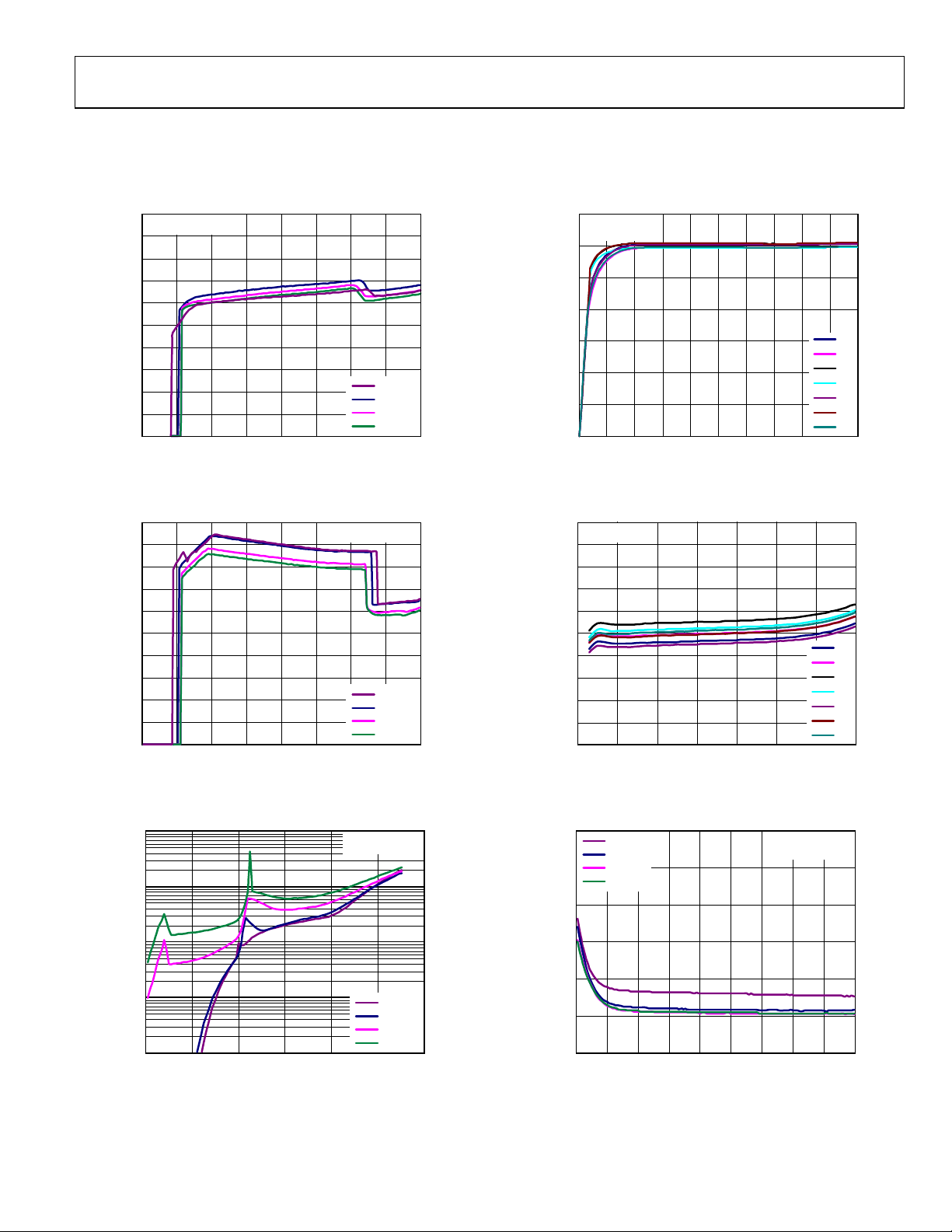
TYPICAL PERFORMANCE CHARACTERISTICS
VIN = 3.6 V, SCL = 2.7 V, SDA = 2.7 V, nRST = 2.7 V, V
T
= 25°C, unless otherwise noted.
A
2.0
I
= NO LOAD
OUT
1.8
1.6
1.4
1.2
1.0
(mA)
Q
I
0.8
0.6
0.4
0.2
0
1.52.02.53.03.54.04.55.05.5
VIN (V)
Figure 5. Typical Quiescent Current, G = 1×
5.0
4.5
4.0
3.5
3.0
2.5
(mA)
Q
I
2.0
1.5
1.0
0.5
0
1.52.02.53.03.54.04.55.05.5
VIN (V)
Figure 6. Typical Quiescent Current, G = 2×, I
10
1
–40°C
+25°C
+85°C
+105°C
I
= NO LOAD
OUT
–40°C
+25°C
+85°C
+105°C
Q(ACTIVE)
SCL = SDA = 0V
nRST = 2. 7V
= 0.4 V, CIN = 1 F, Capacitor C1 = 1 F, Capacitor C2 = 1 F, C
D1:D7
35
VIN = 3.6V
= 30mA
I
D1:D7
30
25
20
(mA)
OUT
I
15
10
5
0
0 0.2 0.4 0.6 0.8 1.0 1.2 1.4 1.6 1.8 2.0
08392-004
VHR (V)
Figure 8. Typical Diode Current vs. Current Sink Headroom Voltage (VHR)
35
V
= 0.4V
D1:D7
34
33
32
31
(mA)
30
OUT
I
29
28
27
26
25
2.0 5.52.5 3.0 3.5 4.0 4.5 5.0
08392-005
VIN (V)
Figure 9. Typical Diode Matching vs. V
6
–40°C
+25°C
+85°C
5
+105°C
4
OUT
IN
VIN = 3.6V
= 30mA
I
D1:D7
= 1 F,
D1
D2
D3
D4
D5
D6
D7
08392-007
D1
D2
D3
D4
D5
D6
D7
08392-008
(µA)
Q
I
0.1
0.01
0.001
–40°C
+25°C
+85°C
+105°C
10 23456
VIN (V)
08392-006
Figure 7. Typical Standby IQ vs. VIN
Rev. A | Page 7 of 52
3
MISMATCH (%)
2
1
0
0.2 2.01.81.61.41.21.00.80.60.4
VHR (V)
08392-009
Figure 10. Typical Diode Matching vs. Current Sink Headroom Voltage (VHR)
Page 8
ADP8863
35
VIN = 3.6V
= 30mA
I
D1:D7
30
25
20
(mA)
OUT
15
I
10
5
0
00.2 2.01.81.61.41.21.00.80.60.4
VHR (V)
–40°C
+25°C
+85°C
+105°C
Figure 11. Typical Diode Current vs. Current Sink Headroom Voltage (VHR)
1
VIN = 3.6V
V
= 0.40V
D1:D7
0
–1
–2
–3
DEVIATIO N ( %)
OUT
I
–4
–5
–6
–40 –10 20 50 80 110
JUNCTION TEM P ERAT URE (°C)
Figure 12. Typical Change In Diode Current vs. Temperature
7
I
= 100mA
OUT
6
5
4
(Ω)
OUT
3
R
2
G = 2× @ V
G = 1.5× @ V
= 2.5V
IN
IN
= 3V
08392-010
08392-011
1.0
0.9
0.8
0.7
0.6
(Ω)
0.5
OUT
R
0.4
0.3
0.2
0.1
0
2.0 2.5 3.0 3.5 4.0 4.5 5.0 5.5
Figure 14. Typical R
VIN (V)
(G = 1×) vs. V
OUT
I
OUT
IN
10
V
= 80% OF V
OUT
9
8
7
6
(mA)
5
OUT
I
4
3
2
1
0
2.0 2.5 3.0 3.5 4.0 4.5 5.0 5.5
IN
VIN (V)
Figure 15. Typical Output Soft Start Current, I
1.4
1.2
1.0
0.8
0.6
THRESHOLD (V)
0.4
VIH @ +25°C
VIH @ +85°C
VIH @ –40°C
= 100mA
–40°C
+25°C
+85°C
+105°C
08392-013
–40°C
+25°C
+85°C
+105°C
08392-014
SS
VIL @ +25°C
VIL @ +85°C
VIL @ –40°C
1
0
–40 –20 0 20 40 60 80 100
G = 1× @ VIN = 3.6V
TEMPERATURE (°C)
Figure 13. R
vs. Temperature
OUT
08392-012
Rev. A | Page 8 of 52
0.2
0
2.5 3.0 3.5 4.0 4.5 5.0 5.5
VIN (V)
Figure 16. Typical I2C Thresholds, VIH and VIL
08392-015
Page 9
ADP8863
1.4
1.3
1.2
1.1
(mA)
ALS
1.0
I
0.9
0.8
0.7
3.02.5 3.5 4.0 4.5 5.0 5.5
VIN (V)
Figure 17. Typical ALS Current, I
5.5
VIN = 3V
GAIN = 2×
5.4
I
= 10mA
OUT
5.3
5.2
5.1
(V)
5.0
OUT
V
4.9
4.8
4.7
4.6
4.5
–10–40 20 50 80 110
JUNCTION TE MPERATURE (° C)
Figure 18. Typical Regulated Output Voltage (V
6.0
5.8
(V)
5.6
OUT
V
OVP THRESHOLD
ALS
–40°C
+25°C
+85°C
+105°C
OUT(REG)
08392-035
08392-016
)
90
80
70
60
50
40
EFFICIENCY (%)
30
20
10
0
2.5 5.55.04.54.03.53.0
100
90
80
70
60
50
40
EFFICIENCY (%)
30
20
10
0
2.5 5.55.04.54.03.53.0
1
2
I
= 140mA, Vf = 3.1V
OUT
I
= 210mA, Vf = 3.2V
OUT
VIN (V)
Figure 20. Typical Efficiency (Low Vf Diode)
I
= 140mA, Vf = 3.85V
OUT
I
= 210mA, Vf = 4.25V
OUT
VIN (V)
Figure 21. Typical Efficiency (High Vf Diode)
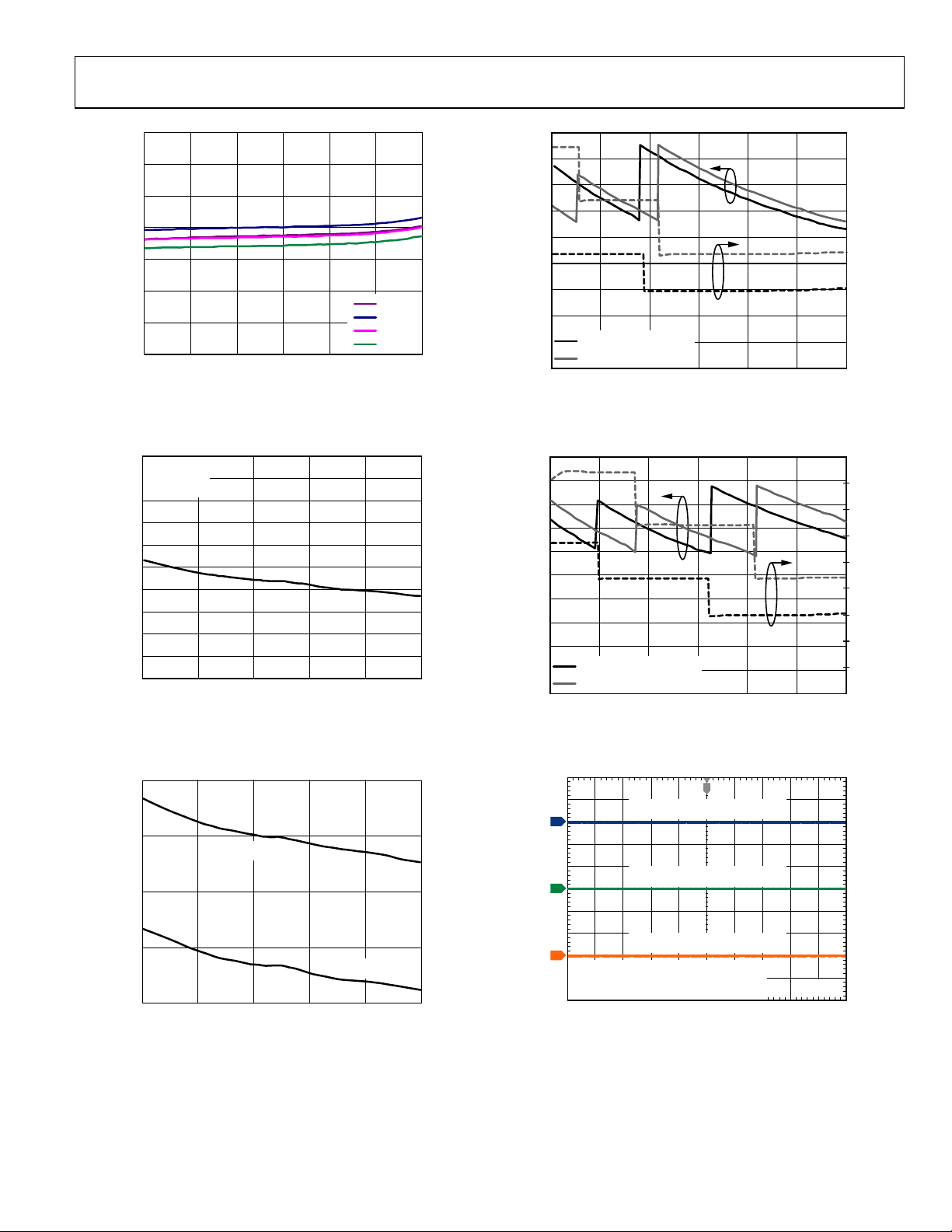
T
VIN (AC-COUPLED) 50 mV /DIV
V
(AC-COUPLED) 50mV/ DI V
OUT
450
400
350
300
250
(mA)
IN
200
I
150
100
50
0
450
400
350
300
250
(mA)
IN
200
I
150
100
50
0
08392-018
08392-019
5.4
OVP RECOVE RY
5.2
–10–40 20 50 80 110
JUNCTION TE MPERATURE (° C)
Figure 19. Typical Overvoltage Protection (OVP) Threshold
08392-017
Rev. A | Page 9 of 52
3
CIN = 1µF, C
V
I
IN
OUT
= 3.6V
= 120mA
IIN (AC-COUPLED) 10mA/DIV
= 1µF, C1 = 1µF, C2 = 1µF
OUT
Figure 22. Typical Operating Waveforms, G = 1×
500ns/DIV
08392-020
Page 10
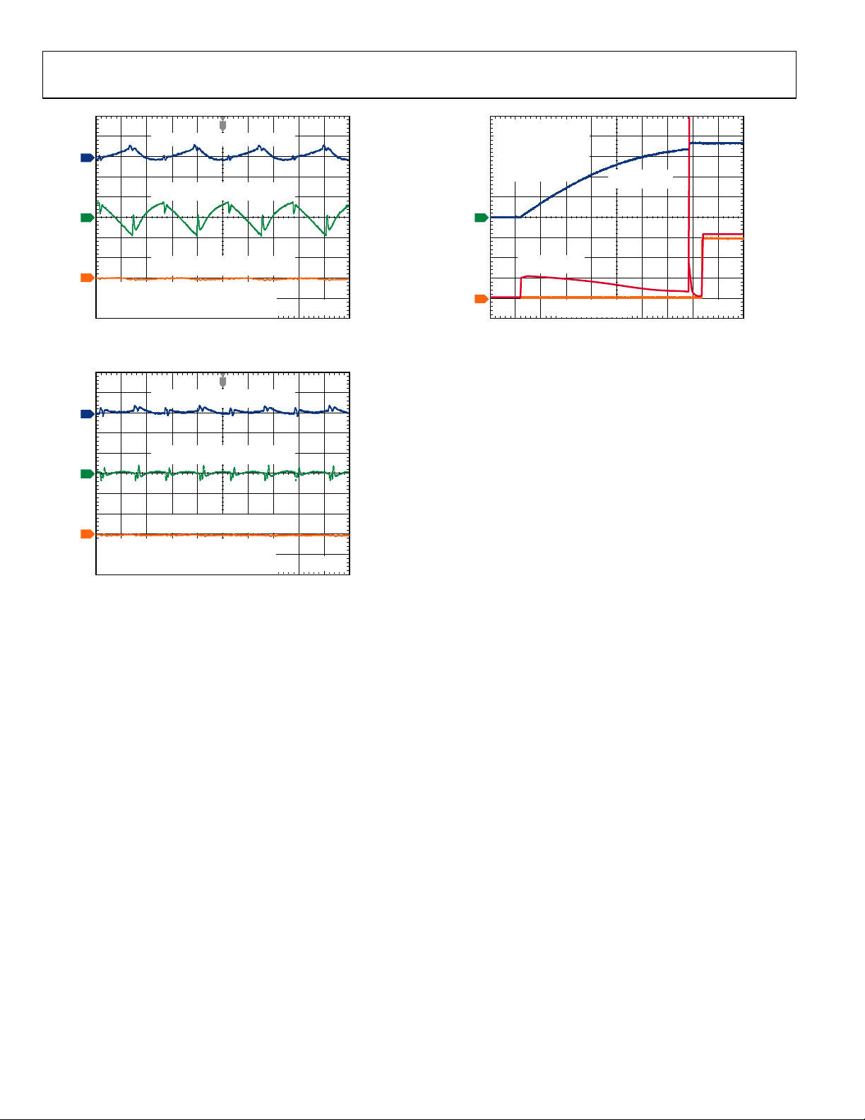
ADP8863
T
VIN (AC-COUPLED) 50mV /DIV
1
V
(AC-COUPLED) 50 mV /DIV
OUT
2
CIN = 10pF, C
C1 = 1µF, C2 = 1µF
= 3.7V
V
IN
= 30mA
I
OUT
(ONE DIODE AT
MAX CURRENT)
2
OUT
= 1µF
V
(1V/DIV)
OUT
3
CIN = 1µF, C
V
I
IN
OUT
= 3.0V
= 120mA
IIN (AC-COUPLED) 10mA/DIV
= 1µF, C1 = 1µF, C2 = 1µF
OUT
Figure 23. Typical Operating Waveforms, G = 1.5×
T
VIN (AC-COUPLED) 50mV /DIV
1
V
(AC-COUPLED) 50 mV /DIV
OUT
2
3
CIN = 1µF, C
V
I
IN
OUT
= 2.5V
= 120mA
IIN (AC-COUPLED) 10mA/DIV
= 1µF, C1 = 1µF, C2 = 1µF
OUT
Figure 24. Typical Operating Waveforms, G = 2×
500ns/DIV
500ns/DIV
IIN (10mA/DIV)
4
08392-021
I
OUT
(10mA/DIV)
100µs/DIV
08392-023
Figure 25. Typical Start-Up Waveform
08392-022
Rev. A | Page 10 of 52
Page 11
ADP8863
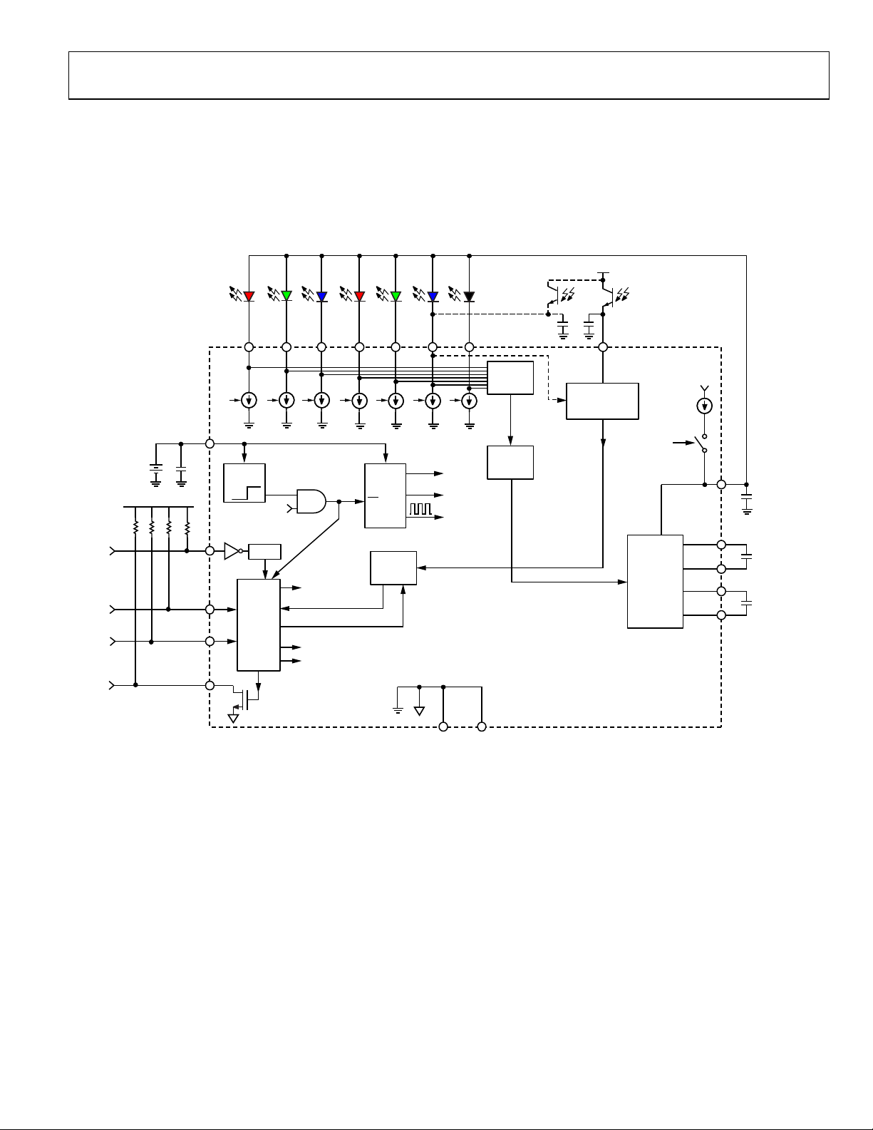
THEORY OF OPERATION
The ADP8863 combines a powerful LED charge pump driver
with independent control of up to seven LEDs. These LED
drivers can sink up to 30 mA (typical) on six channels. The
seventh LED can also be driven to 60 mA (typical). All LEDs
can be individually programmed or combined into a group to
operate backlight LEDs. A full set of safety features, including
short-circuit, overvoltage, and overtemperature protection with
input-to-output isolation, allows for a robust and safe design.
The integrated soft start limits inrush currents at startup, restart
attempts, and gain transitions.
V
ALS
OPTIONAL
PHOTOSENSOR
D4 D5
ID4 ID5
EN
SENSOR
VIN
LIGHT
LOGIC
D6 D7 CMP_IN
GAIN
SELECT
GND2
LOGIC
CHARGE
PUMP
LOGIC
ID6
V
REFS
I
REFS
ID7
CLK
GND1
PHOTOSENSOR
CONVERSION
SOFT ST ART
CHARGE
PUMP
(1×, 1.5×, 2×)
V
IN
I
SS
VOUT
C
OUT
C1+
C1
1µF
C1–
C2+
C2
1µF
C2–
08392-024
VBAT
VDDIO
nRST
SCL
SDA
nINT
VIN
C
IN
D1
ID1
ID2
VIN
STNDBY
NOISE FILTER
50µs
RESET
2
I
C
LOGIC
D2 D3
ID3
UVLO
STANDBY
SWITCH CONTROL
CURRENT SINK CONTROL
Figure 26. Detailed Block Diagram
Rev. A | Page 11 of 52
Page 12

ADP8863
V
POWER STAGE
Because typical white LEDs require up to 4 V to drive them,
some form of boosting is required over the typical variation in
battery voltage. The ADP8863 accomplishes this with a high
efficiency charge pump capable of producing a maximum I
of 240 mA over the entire input voltage range (2.5 V to 5.5 V).
Charge pumps use the basic principle that a capacitor stores
charge based on the voltage applied to it, as shown in the
following equation:
Q = C × V (1)
By charging the capacitors in different configurations, the
charge, and therefore the gain, can be optimized to deliver the
voltage required to power the LEDs. Because a fixed charging
and discharging combination must be used, only certain
multiples of gain are available. The ADP8863 is capable of
automatically optimizing the gain (G) from 1×, 1.5×, and 2×.
These gains are accomplished with two capacitors (labeled C1
and C2 in Figure 26) and an internal switching network.
In G = 1× mode, the switches are configured to pass VIN
directly to VOUT. In this mode, several switches are connected
in parallel to minimize the resistive drop from input to output.
In G = 1.5× and 2× modes, the switches alternatively charge
from the battery and discharge into the output. For G = 1.5×,
the capacitors are charged from V
V
in parallel. For G = 2×, the capacitors are charged from VIN
OUT
in series and are discharged to
IN
OUT
in parallel and are discharged to V
modes, the switches are opened and the output is physically
isolated from the input.
Automatic Gain Selection
Each LED that is driven requires a current source. The voltage
on this current source must be greater than a minimum headroom voltage (200 mV typical) to maintain accurate current
regulation. The gain is automatically selected based on the
minimum voltage (V
) at all of the current sources. At startup,
DX
the device is placed into G = 1× mode and the output charges
to V
. If any VDX level is less than the required headroom
IN
(200 mV), the gain is increased to the next step (G = 1.5×).
A 100 s delay is allowed for the output to stabilize prior to
the next gain switching decision. If there remains insufficient
current sink headroom, then the gain is increased again to 2×.
Conversely, to optimize efficiency, it is not desirable for the
output voltage to be too high. Therefore, the gain reduces when
the headroom voltage is great enough. This point (labeled
V
in Figure 27) is internally calculated to ensure that the
DMAX
lower gain still results in ample headroom for all the current
sinks. The entire cycle is illustrated in Figure 27.
Note that the gain selection criteria apply only to active current
sources. If current sources have been deactivated through an
2
I
C command (for example, only five LEDs are used), then the
voltages on the deactivated current sources are ignored.
in parallel. In certain fault
OUT
STANDBY
EXIT
STARTUP
G = 1
G = 1.5
G = 2
NOTES
1.
IS THE CALCULATED GAIN DOWN TRANSITION PO INT.
DMAX
EXIT ST ANDBY
1
100µs (TYP)
1
WAIT
100µs (TYP)
100µs (TYP)
Figure 27. State Diagram for Automatic Gain Selection
STARTUP:
CHARGE
V
IN
0
VOUT > V
WAIT
WAIT
TO V
OUT
OUT(START)
0
MIN (V
1
1
1
D1:D7
MIN (V
MIN (V
) < V
D1:D7
D1:D7
HR(UP)
) < V
0
) < V
HR(UP)
DMAX
0
MIN (V
0
D1:D7
) > V
DMAX
08392-025
Rev. A | Page 12 of 52
Page 13
ADP8863
Soft Start Feature
At startup (either from UVLO activation or fault/standby
recovery), the output is first charged by I
until it reaches about 92% of V
. This soft start feature reduces
IN
(3.75 mA typical)
SS
the inrush current that is otherwise present when the output
capacitance is initially charged to V
. When this point is
IN
reached, the controller enters G = 1× mode. If the output
voltage is not sufficient, then the automatic gain selection
determines the optimal point as defined in the Automatic Gain
Selection section.
OPERATING MODES
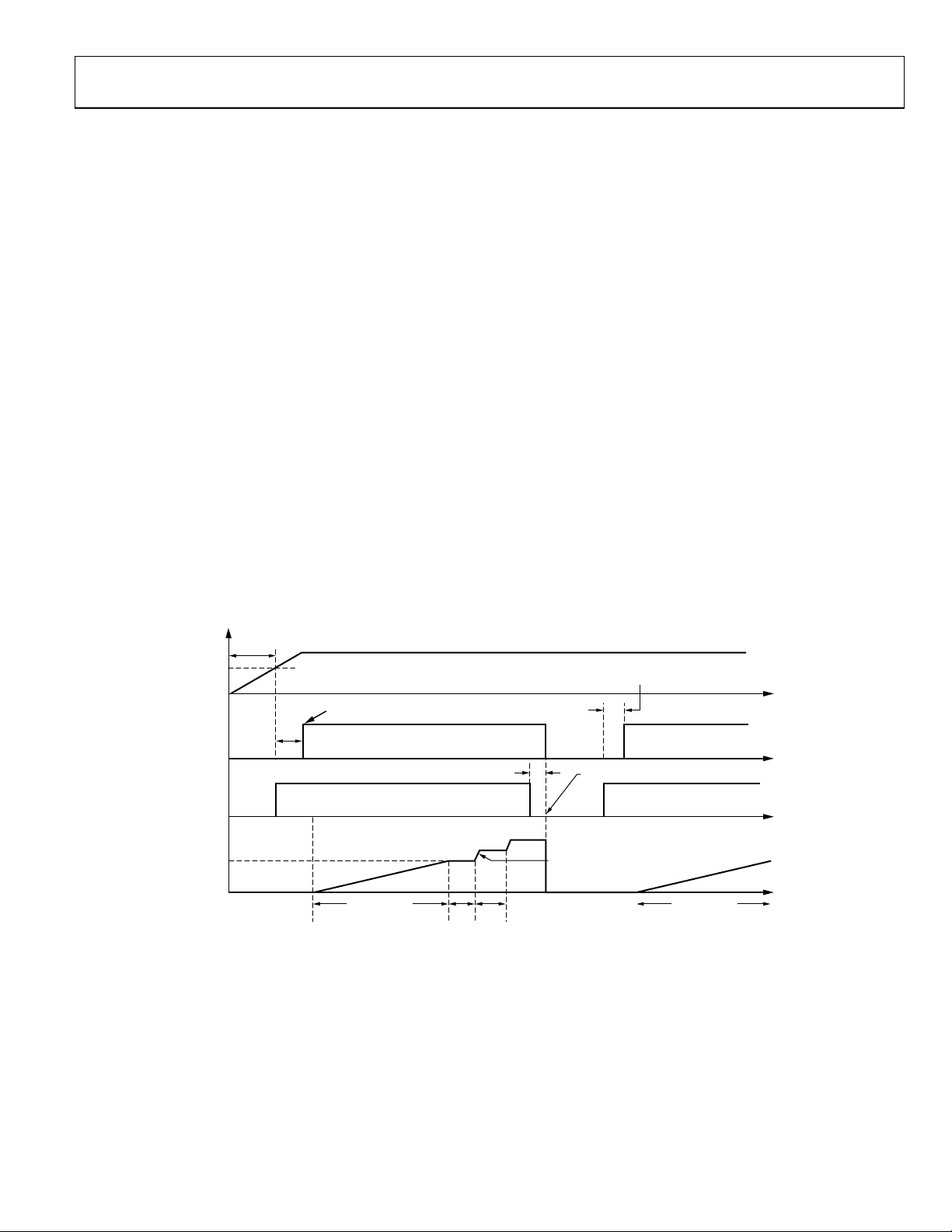
There are four different operating modes: active, standby,
shutdown, and reset.
Active Mode
In active mode, all circuits are powered up and in a fully
operational state. This mode is entered when Bit nSTBY (in
Register MDCR) is set to 1.
Standby Mode
Standby mode disables all circuitry except for the I2C receivers.
Current consumption is reduced to less than 1 A. This mode is
entered when the nSTBY bit is set to 0 or when the nRST pin is
held low for more than 100 s (maximum). When standby is
exited, a soft start sequence is performed.
Shutdown Mode
Shutdown mode disables all circuitry, including the I2C receivers.
Shutdown occurs when V
When V
rises above V
IN
is below the undervoltage thresholds.
IN
(2.05 V typical), all registers are
IN(START)
reset and the part is placed into standby mode.
Reset Mode
In reset mode, all registers are set to their default values and
the part is placed into standby. There are two ways to reset the
part: by power-on reset (POR) or using the nRST pin. POR is
activated any time that the part exits shutdown mode. After a
POR sequence is complete, the part automatically enters
standby mode.
After startup, the part can be reset by pulling the nRST pin low.
As long as the nRST pin is low, the part is held in a standby
state, but no I
2
C commands are acknowledged (all registers are
kept at their default values). After releasing the nRST pin, all
registers remain at their default values, and the part remains in
standby; however, the part does accept I
2
C commands.
The nRST pin has a 50 s (typical) noise filter to prevent inadvertent activation of the reset function. The nRST pin must be
held low for this entire time to activate reset.
The operating modes function according to the timing diagram
in Figure 28.
SHUTDOWN
V
STANDBY
nRST
V
OUT
IN
VINCROSSES ~2.05V AND TRIGGERS POWER-ON RESET
BIT nSTBY IN REGISTER
MDCR GOES LOW
~100µs DELAY BETWEEN POWER-UP AND
2
C COMMANDS CAN BE RECEIVED
WHEN I
25µs TO 100µs NOISE FILTER
~3.75mA CHARGES
V
V
IN
TO VINLEVEL
OUT
1×
10µs 100µs
1.5×
2×
nRST MUST BE HIGH FOR 20µs (MAX)
BEFORE SENDING I
nRST IS LOW, WHICH FORCESSTANDBY
LOW AND RESETS ALL I
GAIN CHANGES OCCUR ONLY W HE N NECESSARY,
BUT HAVE A MIN TIME BEFORE CHANGING
2
CCOMMANDS
2
CREGISTERS
SOFT STARTSOFT START
08392-026
Figure 28. Typical Timing Diagram
Rev. A | Page 13 of 52
Page 14

ADP8863
LED GROUPINGS
Each LED can respond individually or be grouped together
into the backlight controls. By default, all LEDs are set to be
part of the backlight. This is changed by setting Bits[6:0] in
Register 0x05. LEDs that are set up as independent sinks can
be enabled individually in Register 0x10. They can also all be
enabled simultaneously via the SIS_EN bit in Register 0x01.
Any LEDs configured for the backlight can only be enabled
via the BL_EN bit in Register 0x01.
LED CURRENT SETTINGS
Any of the LED outputs (Pin D1 to Pin D7) can be used to
drive any color of LED at 0 mA to 30 mA, provided that the
LED’s Vf is less than 4.1 V. Additionally, the D7 sink can regulate up to 60 mA. The current settings are determined by a
7-bit code programmed by the user into Register 0x14 through
Register 0x1A (for the independent sinks) and Register 0x09 to
Register 0x0E (for the backlight sinks). The 7-bit resolution
allows the user to set the LED to one of 128 different levels.
The ADP8863 can implement two distinct algorithms to
achieve a linear or a nonlinear relationship between input
code and diode output current. The law and SC_LAW bits
in Register 0x04 and Register 0x0F, respectively, are used to
change between these algorithms.
By default, the ADP8863 uses a linear algorithm (law and
SC_LAW = 00), where the LED current increases linearly for
a corresponding increase in input code. LED current (in
milliamperes) is determined by the following equation:
LED Current (mA) = Code × (Full-Scale Current/127) (2)
where:
Code is the input code programmed by the user.
Full-Scale Current is the maximum sink current allowed per
LED (typically 30 mA).
The ADP8863 can also implement a nonlinear (square
approximation) relationship between input code and LED
current. In this case (law and SC_LAW = 01, 10, or 11), the LED
current (in milliamperes) is determined by the following
equation:
2
⎛
⎜
)mA(
×=
CodeCurrentLED
⎜
⎝
−
CurrentScaleFull
127
Figure 29 shows the LED current level vs. input code for both
the linear and square law algorithms.
⎞
⎟
(3)
⎟
⎠
30
25
20
15
10
LED CURRENT (mA)
5
0
0 32 64 96 128
LINEAR
SQUARE
CODE
Figure 29. LED Current vs. Input Code
08392-027
AUTOMATED FADE IN AND FADE OUT
The LED drivers are easily configured for automated fade in
and fade out. Sixteen fade in and fade out rates can be selected
via the I
0.0 sec to 5.5 sec (per full-scale current, either 30 mA or 60 mA).
The backlight LEDs have separate fade in and fade out time
controls from the independent sink LEDs.
Table 5. Available Fade In and Fade Out Rates
Code Fade Rate (in sec per Full-Scale Current)
0000 0.0 (disabled)
0001 0.3
0010 0.6
0011 0.9
0100 1.2
0101 1.5
0110 1.8
0111 2.1
1000 2.4
1001 2.7
1010 3.0
1011 3.5
1100 4.0
1101 4.5
1110 5.0
1111 5.5
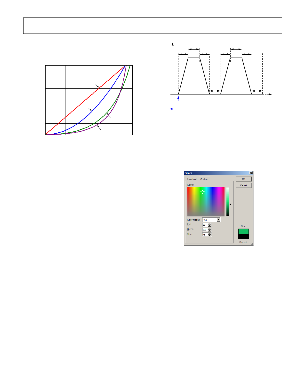
The fade profile is based on the transfer law selected (linear,
square, Cubic 10, or Cubic 11) and the delta between the actual
current and the target current. Smaller changes in current
reduce the fade time. For linear and square law fades, the fade
time is given by
where the Fade Rate is shown in Tabl e 5.
2
C interface. Fade in and fade out rates range from
Fade Time = Fade Rate × (Code/127) (4)
Rev. A | Page 14 of 52
Page 15
ADP8863
The Cubic 10 and Cubic 11 laws also use the square law LED
currents derived from Equation 3; however, the time between
each step is varied to produce a steeper slope at higher currents
and a shallower slope at lower currents (see Figure 30).
30
25
LINEAR
20
15
CURRENT (mA)
10
5
0
00.750.500.25
Figure 30. Comparison of the Dimming Transfers Laws
SQUARE
UNIT FADE TIME
CUBIC 11
CUBIC 10
1.00
08392-028
Each LED can be enabled independently and has its own
current level, but all LEDs share the same fade in rates, fade out
rates, and fade law.
INDEPENDENT SINK CONTROL
Each of the seven LEDs can be configured (in Register 0x05) to
operate as either part of the backlight or to operate as an independent sink current (ISC). Each ISC can be enabled independently
and has its own current level. All ISCs share the same fade in
rates, fade out rates, and fade law.
The ISCs have additional timers to facilitate blinking functions.
A shared on timer (SCON) in conjunction with the off timer of
each ISC (SC1OFF, SC2OFF, SC3OFF, SC4OFF, SC5OFF, SC6OFF,
and SC7OFF) allows the LED current sinks to be configured in
various blinking modes. The on timer can be set to one of four
different settings: 0.2 sec, 0.6 sec, 0.8 sec, or 1.2 sec. The off
timers have four different settings: disabled, 0.6 sec, 1.2 sec, and
1.8 sec. Blink mode is activated by setting the off timers to any
setting other than disabled.
Program all fade, on, and off timers before enabling any of the
LED current sinks. If ISCx is on during a blink cycle and
SCx_EN is cleared, the LED turns off (or fades to off if fade out
is enabled). If ISCx is off during a blink cycle and SCx_EN is
cleared, it stays off.
Rev. A | Page 15 of 52
ISCx
ON TIME ON TIME
FADE-IN FADE-OUT FADE-IN FADE-OUT
MAX
OFF
TIME
SCx_EN
SET BY USER
Figure 31. Independent Sink Blink Mode with Fading
OFF
TIME
RGB COLOR GENERATION
The ADP8863 is easily programmed to generate any color with
an RGB LED. To configure this feature, connect each LED in a
standard RGB diode to a separate driver on the ADP8863.
Because each channel can be programmed for a different
current level, setting the currents for all three LEDs generates
the desired color. To set the current levels, use a simple RGB
color selector (see Figure 32).
08392-036
Figure 32. Standard RGB Color Generator
The example in Figure 32 shows a color of green, which is generated with a red content of 18 (out of 255), a green content of
190, and a blue content of 96. All numbers are out of a maximum
of 255. Thus, the percentage of red is 7.1%, the percentage of
green is 74.5%, and the percentage of blue is 37.6%. To generate
the color with the ADP8863, scale this value to each of the current
drivers.
AUTOMATED RGB COLOR FADES
The ADP8863 is easily programmed to cycle through RGB
generated colors. This can be either a repeating or a random
pattern of one color fading into the other. To execute this cycle
autonomously, set up the RGB LEDs as described in the RGB
Color Generation section and program the on, off, fading times,
and current intensities. Adjusting the fading time in particular
can create any pattern from a fast, striking effect to a soothing
slow color change.
08392-029
Page 16
ADP8863
A
Y
BACKLIGHT OPERATING LEVELS
Backlight brightness control operates at three distinct levels:
daylight (L1), office (L2), and dark (L3). The BLV bits in
Register 0x04 control the specific level at which the backlight
operates. These bits can be changed manually or, if in automatic
mode (CMP_AUTOEN is set high in Register 0x01), by the
ambient light sensor (see the Ambient Light Sensing section).
By default, the backlight operates at daylight level (BLV = 00),
where the maximum brightness is set using Register 0x09
(BLMX1). A daylight dim setting can also be set using Register
0x0A (BLDM1). When operating at office level (BLV = 01), the
backlight maximum and dim brightness settings are set using
Register 0x0B (BLMX2) and Register 0x0C (BLDM2). When
operating at the dark level (BLV = 10), the backlight maximum
and dim brightness settings are set using Register 0x0D (BLMX3)
and Register 0x0E (BLDM3).
D
30mA
BACKLIGHT CURRENT
0
LIGHT (L 1) OFFI CE (L 2) DARK (L 3)
DAYLIGHT_MAX
OFFICE_MAX
DARK_MAX
DAYLIGHT_DIM
OFFICE_DIM
DARK_DIM
BACKLIGHT OPERATING LEVELS
Figure 33. Backlight Operating Levels
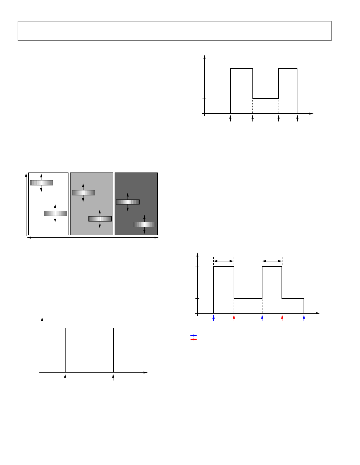
BACKLIGHT TURN ON/TURN OFF/DIM
With the device in active mode (nSTBY = 1), the backlight can
be turned on using the BL_EN bit in Register 0x01. Before
turning on the backlight, select the level (daylight (L1), office
(L2), or dark (L3)) to operate in and ensure that maximum and
dim settings are programmed for that level. The backlight turns
on when BL_EN = 1. The backlight turns off when BL_EN = 0.
BACKLIGHT
CURRENT
MAX
BL_EN = 1 BL_EN = 0
Figure 34. Backlight Turn On/Turn Off
While the backlight is on (BL_EN = 1), the user can change to
the dim setting by programming DIM_EN = 1 in Register 0x01.
If DIM_EN = 0, the backlight reverts to its maximum setting.
8392-038
BACKLIGHT
CURRENT
MAX
DIM
BL_EN = 1
DIM_EN = 1 DIM_EN = 0 BL_ EN = 0
8392-039
Figure 35. Backlight Turn On/Dim/Turn Off
The maximum and dim settings can be set from 0 mA to 30 mA;
therefore, it is possible to program a dim setting that is greater
than a maximum setting. For normal expected operation,
ensure that the dim setting is programmed to be less than the
maximum setting.
AUTOMATIC DIM AND TURN OFF TIMERS
The user can program the backlight to dim automatically by
using the DIMT bits in Register 0x07. The dim timer has 127
settings ranging from 1 sec to 127 sec. Program the dim timer
(DIMT) before turning on the backlight. If BL_EN = 1, the
backlight turns on to its maximum setting and the dim timer
starts counting. When the dim timer expires, the internal state
machine sets DIM_EN = 1, and the backlight enters its dim
08392-037
setting.
BACKLIGHT
CURRENT
MAX
DIM
DIM TIMER
RUNNING
BL_EN = 1 BL_EN = 0DIM_EN = 1 DIM_EN = 0 DIM_E N = 1
SET BY USER
SET BY INTERNAL STATEMACHINE
DIM TIMER
RUNNING
Figure 36. Dim Timer
If the user clears the DIM_EN bit, the backlight reverts to its
maximum setting and the dim timer begins counting again.
When the dim timer expires, the internal state machine again
sets DIM_EN = 1, and the backlight enters its dim setting. The
backlight can be turned off at any point during the dim timer
countdown by clearing BL_EN.
The user can also program the backlight to turn off automatically by using the OFFT bits in Register 0x06. The off timer has
127 settings ranging from 1 sec to 127 sec. Program the off
timer (OFFT) before turning on the backlight. If BL_EN = 1,
the backlight turns on to its maximum setting and the off timer
8392-040
Rev. A | Page 16 of 52
Page 17

ADP8863
starts counting. When the off timer expires, the internal state
machine clears the BL_EN bit, and the backlight turns off.
BACKLIGHT
CURRENT
MAX
SET BY USER
SET BY INTERNAL STATE MACHINE
OFF TIMER
RUNNING
BL_EN = 1 BL_EN = 0
Figure 37. Off Timer
08392-041
The backlight can be turned off at any point during the off
timer countdown by clearing BL_EN.
The dim timer and off timer can be used together for sequential
maximum-to-dim-to-off functionality. With both the dim and
off timers programmed, and BL_EN asserted, the backlight turns
on to its maximum setting, and when the dim timer expires, the
backlight changes to its dim setting. When the off timer expires,
the backlight turns off.
BACKLIGHT
CURRENT
MAX
DIM
SET BY USER
SET BY INTERNA L STATE MACHINE
DIM TIMER
RUNNING
OFF TIMER
RUNNING
BL_EN = 1 BL _E N = 0DIM_EN = 1
Figure 38. Dim and Off Timers Used Together
FADE OVERRIDE
A fade override feature (FOVR in Register CFGR (0x04)) enables
the host to override the preprogrammed fade in or fade out
settings. If FOVR is set and the backlight is enabled in the
middle of a fade out process, the backlight instantly (within
approximately 100 ms) returns to its maximum setting. Alternatively, if the backlight is fading in, reasserting BL_EN overrides
the programmed fade in time, and the backlight instantly goes
to its final fade value. This is useful for situations in which a key
is pressed during a fade sequence. However, if FOVR is cleared
and the backlight is enabled in the middle of a fade process, the
backlight gradually brightens from where it was interrupted (it
does not go down to 0 and then comes back on).
BACKLIGHT
CURRENT
MAX
BL_EN = 1 BL_EN = 0
FADE-IN
OVERRIDDEN
(REASSERTED)
FADE-OUT
OVERRIDDEN
BL_EN = 0BL_EN = 1
BL_EN = 1
08392-043
Figure 39. Fade Override Function (FOVR Is High)
AMBIENT LIGHT SENSING
The ADP8863 integrates two ambient light sensing comparators. One of the ambient light sensing comparator pins
(CMP_IN) is always available. The second pin (D6) has an
ambient light sensor comparator (CMP_IN2) that can be
activated rather than connecting an LED to D6. Activating
the CMP_IN2 function of the pin is accomplished through the
CMP2_SEL bit in Register CFGR. Therefore, when the CMP2_
SEL bit is set to 0, Pin D6 is programmed as a current sink.
When the CMP2_SEL bit is set to 1, Pin D6 becomes the input
for a second phototransistor.
These comparators have two programmable trip points (L2 and
L3) that select one of the three backlight operation modes
(daylight, office, and dark) based on the ambient lighting
conditions.
The L3 comparator controls the dark-to-office mode transition.
The L2 comparator controls the office-to-daylight transition
(see Figure 40). The currents for the different lighting modes
are defined in the BLMXx and BLDMx registers (see the
Backlight Operating Levels Section).
L2_OUT = 1
L3_OUT = 1
08392-042
0 LUX
0A
DARK OFFICE DAYLIGHT
Figure 40. Light Sensor Modes Based on the Detected Ambient Light Level
Each light sensor comparator uses an external capacitor together
with an internal reference current source to form an analog-todigital converter (ADC) that samples the output of the external
photosensor. The ADC result is fed into two programmable trip
comparators. The ADC has an input range of 0 µA to 1080 µA
(typical).
L2_OUT = 1
L3_OUT = 0
L3 L2
BRIGHTNESS
L2_OUT = 0
L3_OUT = 0
08392-044
Rev. A | Page 17 of 52
Page 18

ADP8863
PHOTO
SENSOR
OUTPUT
L2_TRIP
FILTER
SETTINGS
ADC
Figure 41. Ambient Light Sensing and Trip Comparators
L3_TRIP
L2_HYS
L3_HYS
L2_EN
L2_OUT
L3_OUT
L3_EN
The L2 comparator, L2_CMPR, detects when the photosensor
output has dropped below the programmable L2_TRP point
(Register 0x1D). If this event occurs, then the L2_OUT status
signal is set. L2_CMPR contains programmable hysteresis,
meaning that the photosensor output must rise above L2_TRP +
L2_HYS before L2_OUT clears. L2_CMPR is enabled via the
L2_EN bit. The L2_TRP and L2_HYS values of L2_CMPR can
be set between 0 µA and 1080 µA (typical) in steps of 4.3 µA
(typical).
The L3 comparator, L3_CMPR, detects when the photosensor
output drops below the programmable L3_TRP point (Register
0x1F). If this event occurs, the L3_OUT status signal is set.
L3_CMPR contains programmable hysteresis, meaning that the
photosensor output must rise above L3_TRP + L3_HYS before
L3_OUT clears. L3_CMPR is enabled via the L3_EN bit. The
L3_TRP and L3_HYS values of L3_CMPR can be set between
0 µA and 137.7 µA (typical) in steps of 0.54 µA (typical).
L2_TRP
L2_HYS
L3_TRP
L3_HYS
1 10 100 1000
ADC RANGE (µA)
Figure 42. Comparator Ranges
08392-046
Note that the full-scale value of the L2_TRP and L2_HYS
registers is 250 (decimal). Therefore, if the value of L2_TRP +
L2_HYS exceeds 250, the comparator output is unable to
deassert. For example, if L2_TRP is set to 204 (80% of the fullscale value, or approximately 0.80 × 1080 A = 864 A), then
L2_HYS must be set to less than 46 (250 − 204 = 46). If it is not,
then L2_HYS + L2_TRP exceeds 250 and the L2_CMPR
comparator is never allowed to go low.
When both phototransistors are enabled and programmed in
automatic mode (through Bit CMP_AUTOEN in Register
0x01), the user application must determine which comparator
outputs to use, by selecting Bit SEL_AB in Register 0x04 for
automatic light sensing transitions. For example, the user soft-
Rev. A | Page 18 of 52
ware may select the comparator of the phototransistor that is
exposed to higher light intensity to control the transition
between the programmed backlight intensity levels.
The L2_CMPR and L3_CMPR comparators can be enabled
independently of each other, or they can operate simultaneously. A
single conversion from each ADC takes 80 ms (typical). When
CMP_AUTOEN is set for automatic backlight adjustment (see
the Automatic Backlight Adjustment section), the ADC and
comparators run continuously. If the backlight is disabled and
at least one independent sink is enabled, it is possible to use the
light sensor comparators in a single-shot mode. A single-shot read
08392-045
of the photocomparators is performed by setting the FORCE_RD
bit in Register 0x1B. After the single-shot measurement is completed, the internal state machine clears the FORCE_RD bit.
The interrupt flags (CMP_INT and CMP_INT2) can be used to
notify the system when either L2 or L3 changes state. See the
Interrupts section for more information.
AUTOMATIC BACKLIGHT ADJUSTMENT
The ambient light sensor comparators can automatically transition the backlight between one of its three operating levels. To
enable this mode, set the CMP_AUTOEN bit in Register 0x01.
2
When I
control of the BLV bits and changes them based on the L2_OUT
and L3_OUT status bits. When L2_OUT is set high, it indicates
that the ambient light conditions have dropped below the
L2_TRP point and that the backlight should move to its office
(L2) level. When L3_OUT is set high, it indicates that ambient light
conditions have dropped below the L3_TRP point and that the
backlight should move to its dark (L3) level. Ta bl e 6 shows the
relationship between backlight operation and the ambient light
sensor comparator outputs.
The L3_OUT status bit has greater priority; therefore, if
L3_OUT is set, the backlight operates at L3 (dark) even if
L2_OUT is also set.
Filter times from 80 ms to 10 sec can be programmed for the
comparators (Register 0x1B and Register 0x1C) before they
change state.
Table 6. Comparator Output Truth Table
CMP_AUTOEN L3_OUT L2_OUT Backlight Operation
0 X1 X
1 0 0
1 0 1
1 1 X1
1
C selection is enabled, the internal state machine takes
1
BLV can be manually set
by the user
BLV = 00, backlight
operates at L1 (daylight)
BLV = 01, backlight
operates at L2 (office)
BLV = 10, backlight
operates at L3 (dark)
X is the don’t care bit.
Page 19

ADP8863
V
V
USING THE ADP8863 TO DRIVE ADDITIONAL LEDS
In some situations, it may be desirable to drive more than seven
LEDs. This can be done in one of two ways: paralleling LEDs
using ballast resistors, or using the ADP8863 to power
additional LED drivers.
Ballast Resistors
In the first method, multiple LEDs can be attached to any one
LED driver with the use of ballast resistors.
I
1
+
f1
–
Figure 43. Ballast Resistor Arrangement
OUT
I
2
+
Vf2
–
R
BALLASTRBALLASTRBALLAST
V
DX
IDX = I
+
Vf3
–
1 +I2 +I3
I
3
08392-033
Ballast resistors attempt to compensate for the forward voltage
(Vf ) mismatch inherent in any parallel combination of LEDs.
The choice of a ballasting resistor is a trade-off between the
efficiency and the current matching of the LEDs in parallel.
Smaller ballast resistors give better efficiency. Larger ballast
resistors gives better current matching, because the resistor
balances out the current differences for a voltage drop. The
relationship is summarized with the following:
Vf
Δ
R
BALLAST
(5)
≈
I
Δ
where:
ΔVf is the difference between the maximum Vf and the
minimum Vf of the LEDs in parallel.
ΔI is the difference between the parallel LED currents.
The addition of the ballast resistor brings the effective Vf of the
LED to
The I
LED
× R
RILEDVfeffVf ×+= )()(
LED
term forces the charge pump to work a little
BALLAST
(6)
BALLAST
harder for this additional voltage drop. Furthermore, for
guaranteed operation with the ADP8863, the total Vf(eff)
should never exceed V
OUT(REG)
− V
(see Table 1 ).
HR(UP)
VIN
1µF
VDDIO
nRST
VDDIO
SDA
VDDIO
SCL
VDDIO
nINT
Figure 44. Powering Additional LEDs with Ballast Resistors
Adding Additional Parallel Sinks
The ballast resistor’s compromises of efficiency and matching
are not suitable for many applications. Therefore, another
option is to use the ADP8863 charge pump to power additional
current sinks. First, the charge pump must be optimized for this
option by setting the GDWN_DIS bit in Register 0x01, which
prevents the charge pump from switching back down in gain,
and thus stabilizes it against the unknown loads that the
additional current sinks present.
To use the sinks, turn the ADP8863 charge pump on before
activating the additional sinks. If the additional sinks are
activated first, the ADP8863 soft start may not complete.
The ADP8863 can be set up with an ADP8860 or ADP8861. An
example using the ADP8861 is shown in Figure 45.
D2 D3 D4 D5 D6 D7
D1
ADP8863
GND1 GND2
C1+
C1–
C2+
C2–
1µF
VOUT
C1
1µF
C2
1µF
8392-034
Rev. A | Page 19 of 52
Page 20

ADP8863
C
BACKLIGHT
KEYPAD OR
FUN LIGHTING
D2 D3 D4 D5 D6 D7 D1
ADP8863
GNDx
V
MP_IN
nRST
VIN
ALS
SDA
SCL
nINT
1µF
PHOTO
SENSOR
0.1µF
Figure 45. Connecting the ADP8863 to an ADP8861 to Power More LEDs
OPERATING LEDS FROM ALTERNATIVE SUPPLIES
For some applications, it is advantageous to operate the LEDs
from a voltage source other than the ADP8863 charge pump
output. For example, it may be possible to operate a red LED
over the entire battery voltage range without any charge pump
boosting. For a charge pump,
(7)
IN
Therefore, operating the red LEDs directly from the battery
removes output current of the red LEDs from the charge pump
draw. This in turn reduces the total input current by (Gain − 1) ×
I
.
OUT(red)
However, care must be taken when selecting LEDs to operate
from a different voltage input. Specifically, the voltage source
must at least be able to support the maximum forward voltage
(Vf ) of the LED plus the maximum V
Tabl e 1). Additionally, operating an LED from an independent
voltage source may interfere with the ADP8863’s gain selection
algorithm. This algorithm selects the optimal gain for the
charge pump based on all seven diodes. By operating one or
more of the diodes from another supply, the algorithm may not
switch the gain back down to a lower state until the LEDs are
disabled or the part enters standby.
IGainI ×=
OUT
(276 mV, given in
HR(UP)
C1+
C1–
C2+
C2–
VOUT
1µF
C1
1µF
C2
1µF
VIN
nRST
SDA
SCL
nINT
nRST
SDA
SCL
nINT
VIN
1µF
1µF
VDDIO
VDDIO
VDDIO
VDDIO
D2 D3 D4 D5 D6 D7 D1
ADP8861
GNDx
D1 D2 D3 D4 D5 D6 D7
C1+
C1–
C2+
C2–
ADP8863
GND1 GND2
Figure 46. Alternate Schematic for Low Vf LEDs
VOUT
NC
NC
NC
NC
C1+
C1–
C2+
C2–
1µF
08392-047
VOUT
C1
1µF
C2
1µF
8392-030
Rev. A | Page 20 of 52
Page 21

ADP8863
SHORT-CIRCUIT PROTECTION MODE
The ADP8863 can protect against short circuits on the output
(VOUT). Short-circuit protection (SCP) is activated at the point
when VOUT < 55% of V
. Note that SCP sensing is disabled
IN
during both startup and restart attempts (fault recovery). SCP
sensing is reenabled 4 ms (typical) after activation. During a
short-circuit fault, the device enters a low current consumption
state and an interrupt flag is set. The device can be restarted at any
time after receiving a short-circuit fault by rewriting nSTBY = 1.
It then repeats another complete soft start sequence. Note that
the value of the output capacitance (C
) should be small
OUT
enough to allow VOUT to reach approximately 55% (typical) of
V
within the 4 ms (typical) time. If C
IN
is too large, the device
OUT
inadvertently enters short-circuit protection.
OVERVOLTAGE PROTECTION
Overvoltage protection (OVP) is implemented on the output.
There are two types of overvoltage events: normal (no fault) and
abnormal (from a fault or sudden load change).
Normal Overvoltage
In a normal (no fault) overvoltage, the output voltage approaches
V
caused by a fault or load change, but is simply a consequence of
the input voltage times the gain reaching the same level as the
clamped output voltage (V
overvoltage, the ADP8863 detects when the output voltage rises
to V
to reduce the voltage that is delivered. This effectively regulates
V
system can have on regulating V
normal operation and it is not intended to protect against faults
or sudden load changes. When the output voltage is regulated to
V
the LEDs and the overall application.
Abnormal Overvoltage
Because of the open-loop behavior of the charge pump as well
as how the gain transitions are computed, a sudden load change
or fault can abnormally force V
abnormal overvoltage situation. If the event happens slowly
enough, the system first tries to regulate the output to 4.9 V as
in a normal overvoltage scenario. However, if this is not sufficient, or if the event happens too quickly, the ADP8863 enters
overvoltage protection (OVP) mode when V
OVP threshold (typically 5.8 V). In OVP mode, only the charge
pump is disabled to prevent V
(4.9 V typical) during normal operation. This is not
OUT(REG)
). To prevent this type of
OUT(REG)
. It then increases the effective R
OUT(REG)
to V
OUT
, no interrupt is set and the operation is transparent to
OUT(REG)
; however, there is a limit to the effect that this
OUT(REG)
. It is designed only for
OUT
beyond 6 V. This causes an
OUT
from rising too high. The
OUT
of the gain stage
OUT
OUT
exceeds the
current sources and all other device functionality remain intact.
When the output voltage falls by about 500 mV (to 5.3 V
typical), the charge pump resumes operation. If the fault or load
event recurs, the process may repeat. An interrupt flag is set at
each OVP instance.
THERMAL SHUTDOWN/OVERTEMPERATURE PROTECTION
If the die temperature of the ADP8863 rises above a safe limit
(150°C typical), the controllers enter thermal shutdown (TSD)
protection mode. In this mode, most of the internal functions
shut down, the part enters standby, and the TSD_INT interrupt
(Register 0x02) is set. When the die temperature decreases
below ~130°C, the part can be restarted. To restart the part,
remove it from standby. No interrupt is generated when the die
temperature falls below 130°C. However, if the software clears
the pending TSD_INT interrupt and the temperature remains
above 130°C, another interrupt is generated.
The complete state machine for these faults (SCP, OVP, and
TSD) is shown in Figure 47.
INTERRUPTS
There are five interrupt sources available on the ADP8863 in
Register 0x02.
• Main light sensor comparator: The CMP_INT interrupt
sets every time the main light sensor comparator detects a
threshold (L2 or L3) transition (rising or falling condition).
• Sensor Comparator 2: The CMP2_INT interrupt works
the same way as CMP_INT, except that the sensing input
derives from the second light sensor. The programmable
thresh-olds are the same as for the main light sensor
comparator.
• Overvoltage protection: OVP_INT is generated when the
output voltage exceeds 5.8 V (typical).
• Thermal shutdown circuit: an interrupt (TSD_INT) is
generated when entering overtemperature protection.
• Short-circuit detection: SHORT_INT is generated when
the device enters short-circuit protection mode.
The interrupt (if any) that appears on the nINT pin is determined by the bits mapped in Register INTR_EN (0x03). To
clear an interrupt, write a 1 to the interrupt in the MDCR2
register (0x02) or reset the part. Reading the interrupt, or writing a
0, has no effect.
Rev. A | Page 21 of 52
Page 22

ADP8863
VOUT < V
V
OVP(HYS)
OVP FAULT
OVP
STANDBY
EXIT ST ANDBY
0
1
TSD FAULT
0
(HYS)
EXIT STBY
STARTUP:
CHARGE
VIN TO VOUT
SCP FAULT
DIE TEMP > TSD
1
DIE TEMP <
TSD – TSD
0
VOUT > V
OUT(START)
1
0
EXIT
STARTUP
VOUT < V
OUT(SC)
0
–
0
1
VOUT > V
OVP
0
G = 1
WAIT
100µs (TY P )
1
MIN (V
< V
1
D1:D7
HR(UP)
)
1
0
0
MIN (V
> V
D1:D7
DMAX
)
VOUT < V
V
OVP(HYS)
OVP FAULT
1
VOUT > V
OVP
OVP
1
–
0
VOUT > V
0
OUT(REG)
G = 1.5
WAIT
100µs (TYP)
MIN (V
< V
D1:D7
HR(UP)
)
1
0
TRY TO
REGULATE
VOUT TO
V
OUT(REG)
1
1
0
1
VOUT > V
TRY TO
REGULATE
VOUT TO
V
OUT(REG)
OUT(REG)
1
0
G = 2
NOTES
1. V
IS THE CALCULATED GAI N DO WN TRANSIT I ON POINT .
DMAX
Figure 47. Fault State Machine
V
OVP(HYS)
OVP
–
VOUT < V
0
OVP FAULT
0
1
VOUT > V
OVP
WAIT
100µs (TYP)
MIN (V
> V
D1:D7
DMAX
)
08392-031
Rev. A | Page 22 of 52
Page 23

ADP8863
V
APPLICATIONS INFORMATION
The ADP8863 allows the charge pump to operate efficiently with a
minimum of external components. Specifically, the user must
select an input capacitor (C
charge pump fly capacitors (C1 and C2). C
), output capacitor (C
IN
should be 1 F or
IN
), and two
OUT
greater. The value must be high enough to produce a stable input
voltage signal at the minimum input voltage and maximum
output load. A 1 F capacitor for C
is recommended. Larger
OUT
values are permissible, but care must be exercised to ensure that
VOUT charges above 55% (typical) of V
within 4 ms (typical).
IN
See the Short-Circuit Protection Mode section for more details.
For best practice, it is recommended that the two charge pump fly
capacitors be 1 F; larger values are not recommended, and smaller
values may reduce the ability of the charge pump to deliver
maximum current. For optimal efficiency, the charge pump fly
capacitors should have low equivalent series resistance (ESR). Low
ESR X5R or X7R capacitors are recommended for all four components. The use of fly capacitors sized 0402 and smaller is allowed,
but the GDWN_DIS bit in Register 0x01 must be set. Minimum
voltage ratings should adhere to the guidelines in Table 7.
Table 7. Capacitor Stress in Each Charge Pump Gain State
Capacitor Gain = 1× Gain = 1.5× Gain = 2×
CIN V
C
V
OUT
C1 None VIN/2 VIN
C2 None VIN/2 VIN
V
IN
V
IN
V
IN
× 1.5 (max of 5.5 V) VIN × 2.0 (max of 5.5 V)
IN
IN
If one or both ambient light sensor comparator inputs (CMP_IN
and D6) are used, a small capacitor (0.1 F is recommended)
must be connected from the input to ground.
Any color LED can be used if the Vf (forward voltage) is less
than 4.1 V. However, using lower Vf LEDs reduces the input
power consumption by allowing the charge pump to operate at
lower gain states.
The equivalent circuit model for a charge pump is shown in
Figure 48.
OUT
R
OUT
G × V
Figure 48. Charge Pump Equivalent Circuit Model
I
OUT
V
DX
C
OUT
IN
08392-032
The input voltage is multiplied by the gain (G) and delivered to
the output through an effective resistance (R
current flows through R
= G ×VIN − I
V
OUT
The R
term is a combination of the R
OUT
and produces an IR drop to yield
OUT
× R
OUT
(G) (8)
OUT
DSON
). The output
OUT
resistance for the
switches used in the charge pump and a small resistance that accounts
for the effective dynamic charge pump resistance. The R
OUT
level
changes based upon the gain (the configuration of the switches).
Typical R
V
OUT
values are given in Tab l e 1 , Figure 13, and Figure 14.
OUT
is also equal to the largest Vf of the LEDs used plus the
voltage drop across the regulating current source. This gives
V
OUT
= Vf
+ VDX (9)
(MAX)
Combining Equation 8 and Equation 9 gives
V
= (Vf
IN
(MAX)
+ VDX + I
OUT
× R
(G))/G (10)
OUT
Equation 10 is useful for calculating approximate bounds for the
charge pump design.
Determining the Transition Point of the Charge Pump
Consider the following design example, where:
Vf
= 3.7 V
(MAX)
I
= 140 mA (7 LEDs at 20 mA each)
OUT
(G = 1.5×) = 3 Ω (obtained from Figure 13)
R
OUT
At the point of a gain transition, V
typical value of V
as 0.2 V. Therefore, the input voltage
HR(UP)
DX
= V
. Tabl e 1 gives the
HR(UP)
level when the gain transitions from 1.5× to 2× is
V
= (3.7 V + 0.2 V + 140 mA × 3 Ω)/1.5 = 2.88 V
IN
LAYOUT GUIDELINES
Note the following layout guidelines:
• For optimal noise immunity, place the C
tors as close as possible to their respective pins. These
capacitors should share a short ground trace. If the LEDs
are a significant distance from the VOUT pin, another capacitor on VOUT, placed closer to the LEDs, is advisable.
• For optimal efficiency, place the charge pump fly capacitors
(C1 and C2) as close to the part as possible.
• The ADP8863 does not distinguish between power ground
and analog ground. Therefore, both ground pins can be
connected directly together. It is recommended that these
ground pins be connected at the ground for the input and
output capacitors.
• The LFCSP package requires the exposed pad to be
soldered at the board to the GND1 and/or GND2 pin(s).
• Unused diode pins (Pin D1 to Pin D7) can be connected to
ground or to VOUT, or remain floating. However, the
unused diode current sinks must be disabled by setting
them as independent sinks in Register 0x05 and then
disabling them in Register 0x10. If they are not disabled,
the charge pump efficiency may suffer.
• If the CMP_IN phototransistor input is not used, it can be
connected to ground or remain floating.
• If the interrupt pin (nINT) is not used, connect it to ground
or leave it floating. Never connect it to a voltage supply,
except through a ≥1 k series resistor.
• The ADP8863 has an integrated noise filter on the nRST
pin. Under normal conditions, it is not necessary to filter
the reset line. However, if the part is exposed to an unusually
noisy signal, it is beneficial to add a small RC filter or bypass
capacitor on this pin. If the nRST pin is not used, it must
be pulled well above the V
level (see Table 1). Do not
IH(MIN)
allow the nRST pin to float.
and C
IN
OUT
capaci-
Rev. A | Page 23 of 52
Page 24

ADP8863
I2C PROGRAMMING AND DIGITAL CONTROL
The ADP8863 provides full software programmability to facilitate its adoption in various product architectures. The I
2
C address
is 0101011x (x = 0 during write, x = 1 during read). Therefore,
the write address is 0x56 and the read address is 0x57.
Note the following general behavior of registers:
• All registers are set to their default values during reset or
after a UVLO event.
• All registers are read/write unless otherwise specified.
• Unused bits are read as zero.
0101011
ST ACK ACK
R/W
Tabl e 8 to Ta b le 8 4 provide register and bit descriptions. The
reset value for all bits in the bit map tables is all 0s, except in
Tabl e 10 (see Table 1 0 for its unique reset value). Wherever the
acronym N/A appears in the tables, it means not applicable.
B0B7B0B7B0B7
REGISTER VALUEREGISTE R ADDRE SS
ACK
ST
START
SLAVE TO MASTER
MASTER TO SLAVE
DEVICE ID
FOR WRITE
OPERATION
SELECT REGISTER TO WRITE
WRITE = 0
FROM ADP8863
Figure 49. I
2
C Write Sequence
8-BIT VALUE TO WRITE IN THE
ADDRESSED REGISTER
FROM ADP8863
FROM ADP8863
STOP
08392-048
B0B7B0B7B0B7B0B7
ST
DEVICE ID
FOR WRITE
START
OPERATION
SLAVE TO MASTER
MASTER TO SLAVE
R/W
ACK ACK ACK ACK0101011 STRS0101011
REGISTE R ADDRES S REGISTE R VALUE
SELECT REGISTER TO WRITE
WRITE = 0
FROM ADP8863
Figure 50. I
FROM ADP8863
REPEATED START
2
C Read Sequence
DEVICE ID
FOR READ
OPERATION
R/W
8-BIT VALUE TO WRITE IN THE
READ = 1
ADDRESSED REGISTER
FROM ADP8863
STOP
FROM MASTER
08392-049
Rev. A | Page 24 of 52
Page 25

ADP8863
Table 8. Register Set Definitions
Address (Hex) Register Name Description
0x00 MFDVID Manufacturer and device ID
0x01 MDCR Device mode and status
0x02 MDCR2 Device mode and Status Register 2
0x03 INTR_EN Interrupts enable
0x04 CFGR Configuration register
0x05 BLSEN Sink enable, backlight or independent
0x06 BLOFF Backlight off timeout
0x07 BLDIM Backlight dim timeout
0x08 BLFR Backlight fade in and fade out rates
0x09 BLMX1 Backlight (brightness Level 1—daylight) maximum current
0x0A BLDM1 Backlight (brightness Level 1—daylight) dim current
0x0B BLMX2 Backlight (brightness Level 2—office) maximum current
0x0C BLDM2 Backlight (brightness Level 2—office) dim current
0x0D BLMX3 Backlight (brightness Level 3—dark) maximum current
0x0E BLDM3 Backlight (brightness Level 3—dark) dim current
0x0F ISCFR Independent sink current fade control register
0x10 ISCC Independent sink current control register
0x11 ISCT1 Independent sink current timer register, LED[7:5]
0x12 ISCT2 Independent sink current timer register, LED[4:1]
0x13 ISCF Independent sink current fade register
0x14 ISC7 Independent sink current, LED7
0x15 ISC6 Independent sink current, LED6
0x16 ISC5 Independent sink current, LED5
0x17 ISC4 Independent sink current, LED4
0x18 ISC3 Independent sink current, LED3
0x19 ISC2 Independent sink current, LED2
0x1A ISC1 Independent sink current, LED1
0x1B CCFG Comparator configuration
0x1C CCFG2 Second comparator configuration
0x1D L2_TRP L2 comparator reference
0x1E L2_HYS L2 hysteresis
0x1F L3_TRP L3 comparator reference
0x20 L3_HYS L3 hysteresis
0x21 PH1LEVL First phototransistor ambient light level—low byte register
0x22 PH1LEVH First phototransistor ambient light level—high byte register
0x23 PH2LEVL Second phototransistor ambient light level—low byte register
0x24 PH2LEVH Second phototransistor ambient light level—high byte register
Rev. A | Page 25 of 52
Page 26

ADP8863
Table 9. Register Map
Addr
(Hex) Reg. Name Bit 7 Bit 6 Bit 5 Bit 4 Bit 3 Bit 2 Bit 1 Bit 0
0x00 MFDVID Manufacturer ID Device ID
0x01 MDCR Reserved INT_CFG nSTBY DIM_EN GDWN_DIS SIS_EN CMP_AUTOEN BL_EN
0x02 MDCR2 Reserved SHORT_INT TSD_INT OVP_INT CMP2_INT CMP_INT
0x03 INTR_EN Reserved SHORT_IEN TSD_IEN OVP_IEN CMP2_IEN CMP_IEN
0x04 CFGR Reserved SEL_AB CMP2_SEL BLV Law FOVR
0x05 BLSEN Reserved D7EN D6EN D5EN D4EN D3EN D2EN D1EN
0x06 BLOFF Reserved OFFT
0x07 BLDIM Reserved DIMT
0x08 BLFR BL_FO BL_FI
0x09 BLMX1 Reserved BL1_MC
0x0A BLDM1 Reserved BL1_DC
0x0B BLMX2 Reserved BL2_MC
0x0C BLDM2 Reserved BL2_DC
0x0D BLMX3 Reserved BL3_MC
0x0E BLDM3 Reserved BL3_DC
0x0F ISCFR Reserved SC_LAW
0x10 ISCC Reserved SC7_EN SC6_EN SC5_EN SC4_EN SC3_EN SC2_EN SC1_EN
0x11 ISCT1 SCON SC7OFF SC6OFF SC5OFF
0x12 ISCT2 SC4OFF SC3OFF SC2OFF SC1OFF
0x13 ISCF SCFO SCFI
0x14 ISC7 SCR SCD7
0x15 ISC6 Reserved SCD6
0x16 ISC5 Reserved SCD5
0x17 ISC4 Reserved SCD4
0x18 ISC3 Reserved SCD3
0x19 ISC2 Reserved SCD2
0x1A ISC1 Reserved SCD1
0x1B CCFG FILT FORCE_RD L3_OUT L2_OUT L3_EN L2_EN
0x1C CCFG2 FILT2 FORCE_RD2 L3_OUT2 L2_OUT2 L3_EN2 L2_EN2
0x1D L2_TRP L2_TRP
0x1E L2_HYS L2_HYS
0x1F L3_TRP L3_TRP
0x20 L3_HYS L3_HYS
0x21 PH1LEVL PH1LEV_LOW
0x22 PH1LEVH Reserved PH1LEV_HIGH
0x23 PH2LEVL PH2LEV_LOW
0x24 PH2LEVH Reserved PH2LEV_HIGH
Rev. A | Page 26 of 52
Page 27

ADP8863
Manufacturer and Device ID (MFDVID)—Register 0x00
This is a read-only register.
Table 10. MFDVID Bit Map
Bit 7 Bit 6 Bit 5 Bit 4 Bit 3 Bit 2 Bit 1 Bit 0
Manufacturer ID Device ID
0 0 1 0 1 0 1 0
Mode Control Register (MDCR)—Register 0x01
Table 11. MDCR Bit Map
Bit 7 Bit 6 Bit 5 Bit 4 Bit 3 Bit 2 Bit 1 Bit 0
Reserved INT_CFG nSTBY DIM_EN GDWN_DIS SIS_EN CMP_AUTOEN BL_EN
Table 12. Bit Descriptions for the MDCR Register
Bit Name Bit No. Description
N/A 7 Reserved.
INT_CFG 6 Interrupt configuration.
1 = processor interrupt deasserts for 50 s and reasserts with pending events.
0 = processor interrupt remains asserted if the host tries to clear the interrupt while there is a pending event.
nSTBY 5 1 = device is in active mode.
0 = device is in standby mode; only the I2C interface is enabled.
DIM_EN 4
1 = backlight is operating at the dim current level (BL_EN must also be asserted).
0 = backlight is not in dim mode.
GDWN_DIS 3 Gain down disable bit. Setting this bit does not allow the charge pump to switch to lower gains.
SIS_EN 2 Synchronous independent sinks enable.
CMP_AUTOEN 1
BL_EN 0 1 = backlight is enabled (nSTBY must also be asserted).
0 = backlight is disabled.
DIM_EN is set by the hardware after a dim timeout. The user may also force the backlight into dim mode by
asserting this bit. Dim mode can only be entered if BL_EN is also enabled.
1 = the charge pump does not switch down in gain until all LEDs are off. The charge pump switches up in gain as
needed. This feature is useful if the ADP8863 charge pump is used to drive an external load. This feature must be
used when utilizing small fly capacitors (0402 or smaller).
0 = the charge pump automatically switches up and down in gain. This provides optimal efficiency, but is not
suitable for driving loads that are not connected through the ADP8863 diode drivers. Additionally, the charge
pump fly capacitors should be low ESR and sized 0603 or greater.
1 = enables all LED current sinks designated as independent sinks. All of the ISC enable bits must be cleared;
if any of the SCx_EN bits in Register 0x10 are set, this bit has no effect.
0 = disables all sinks designated as independent sinks. All of the ISC enable bits must be cleared; if any of the
SCx_EN bits in Register 0x10 are set, this bit has no effect.
1 = backlight automatically responds to the comparator outputs (L2_OUT and L3_OUT). L2_EN and/or L3_EN
must be set for this to function. BLV values in Register 0x04 are overridden.
0 = backlight does not respond automatically to comparator level changes. The user can manually select
backlight operating levels using Bit BLV in Register 0x04.
Rev. A | Page 27 of 52
Page 28

ADP8863
Mode Control Register 2 (MDCR2)—Register 0x02
Table 13. MDCR2 Bit Map
Bit 7 Bit 6 Bit 5 Bit 4 Bit 3 Bit 2 Bit 1 Bit 0
Reserved SHORT_INT TSD_INT OVP_INT CMP2_INT CMP_INT
Table 14. Bit Descriptions for the MDCR2 Register
Bit Name Bit No. Description1
N/A [7:5] Reserved.
SHORT_INT 4 Short-circuit error interrupt.
1 = a short-circuit or overload condition on VOUT has been detected.
0 = no short-circuit or overload condition has been detected.
TSD_INT 3 Thermal shutdown interrupt.
1 = the device temperature has exceeded 150°C (typical).
0 = no overtemperature condition has been detected.
OVP_INT 2 Overvoltage interrupt.
1 = VOUT has exceeded V
0 = VOUT has not exceeded V
CMP2_INT 1 1 = the second ALS comparator (CMP_IN2) has changed state.
0 = the second sensor comparator has not been triggered.
CMP_INT 0 1 = main ALS comparator (CMP_IN) has changed state.
0 = the main sensor comparator has not been triggered.
1
Interrupt bits are cleared by writing a 1 to the flag; writing a 0 or reading the flag has no effect.
Interrupt Enable (INTR_EN)—Register 0x03
OVP
.
.
OVP
Table 15. INTR_EN Bit Map
Bit 7 Bit 6 Bit 5 Bit 4 Bit 3 Bit 2 Bit 1 Bit 0
Reserved SHORT_IEN TSD_IEN OVP_IEN CMP2_IEN CMP_IEN
Table 16. Bit Descriptions for the INTR_EN Register
Bit Name Bit No. Description
N/A [7:5] Reserved.
SHORT_IEN 4
Short-circuit interrupt is enabled. When the SHORT_INT status bit is set after an error condition, an interrupt is
raised to the host if the SHORT_IEN flag is enabled.
1 = the short-circuit interrupt is enabled.
0 = the short-circuit interrupt is disabled (the SHORT_INT flag continues to assert).
TSD_IEN 3
Thermal shutdown interrupt is enabled. When the TSD_INT status bit is set after an error condition, an interrupt is
raised to the host if the TSD_IEN flag is enabled.
1 = the thermal shutdown interrupt is enabled.
0 = the thermal shutdown interrupt is disabled (the TSD_INT flag continues to assert).
OVP_IEN 2
Overvoltage interrupt enabled. When the OVP_INT status bit is set after an error condition, an interrupt is raised to
the host if the OVP_IEN flag is enabled.
1 = the overvoltage interrupt is enabled.
0 = the overvoltage interrupt is disabled (the OVP_INT flag continues to assert).
CMP2_IEN 1
When the CMP2_INT status bit is set after an enabled comparator trips, an interrupt is raised if the CMP2_IEN flag is
enabled.
1 = the second phototransistor comparator interrupt is enabled.
0 = the second phototransistor comparator interrupt is disabled (the CMP2_INT flag continues to assert).
CMP_IEN 0
When the CMP_INT status bit is set after an enabled comparator trips, an interrupt is raised if the CMP_IEN flag is
enabled.
1 = the main comparator interrupt is enabled.
0 = the main comparator interrupt is disabled (the CMP_INT flag continues to assert).
Rev. A | Page 28 of 52
Page 29

ADP8863
BACKLIGHT REGISTER DESCRIPTIONS
Configuration Register (CFGR)—Register 0x04
Table 17. CFGR Bit Map
Bit 7 Bit 6 Bit 5 Bit 4 Bit 3 Bit 2 Bit 1 Bit 0
Reserved SEL_AB CMP2_SEL BLV Law FOVR
Table 18. Bit Descriptions for the CFGR Register
Bit Name Bit No. Description
N/A 7 Reserved.
SEL_AB 6 1 = selects the second phototransistor (CMP_IN2) to control the backlight.
0 = selects the main phototransistor (CMP_IN) to control the backlight.
CMP2_SEL 5 1 = the second phototransistor is enabled; the current sink on D6 is disabled.
0 = the second phototransistor is disabled.
BLV [4:3]
00 = Level 1 (daylight).
01 = Level 2 (office).
10 = Level 3 (dark).
11 = off (backlight set to 0 mA).
Law [2:1] Backlight transfer law.
00 = linear law DAC, linear time steps.
01 = square law DAC, linear time steps.
10 = square law DAC, nonlinear time steps (Cubic 10).
11 = square law DAC, nonlinear time steps (Cubic 11).
FOVR 0 Backlight fade override.
1 = the backlight fade override is enabled.
0 = the backlight fade override is disabled.
Brightness level. This field indicates the brightness level at which the device is operating. The software may force the
backlight to operate at one of the three brightness levels. Setting CMP_AUTOEN high (Register 0x01) sets these
values automatically and overwrites any previously written values.
Backlight Sink Enable (BLSEN)—Register 0x05
Table 19. BLSEN Bit Map
Bit 7 Bit 6 Bit 5 Bit 4 Bit 3 Bit 2 Bit 1 Bit 0
Reserved D7EN D6EN D5EN D4EN D3EN D2EN D1EN
Table 20. Bit Descriptions for the BLSEN Register
Bit Name Bit No. Description
N/A 7 Reserved
D7EN 6 Diode 7 backlight sink enable
1 = selects LED7 as an independent sink
0 = connects LED7 sink to backlight enable (BL_EN)
D6EN 5 Diode 6 backlight sink enable
1 = selects LED6 as an independent sink
0 = connects LED6 sink to backlight enable (BL_EN)
D5EN 4 Diode 5 backlight sink enable
1 = selects LED5 as an independent sink
0 = connects LED5 sink to backlight enable (BL_EN)
D4EN 3 Diode 4 backlight sink enable
1 = selects LED4 as an independent sink
0 = connects LED4 sink to backlight enable (BL_EN)
D3EN 2 Diode 3 backlight sink enable
1 = selects LED3 as an independent sink
0 = connects LED3 sink to backlight enable (BL_EN)
Rev. A | Page 29 of 52
Page 30

ADP8863
Bit Name Bit No. Description
D2EN 1 Diode 2 backlight sink enable
1 = selects LED2 as an independent sink
0 = connects LED2 sink to backlight enable (BL_EN)
D1EN 0 Diode 1 backlight sink enable
1 = selects LED1 as an independent sink
0 = connects LED1 sink to backlight enable (BL_EN)
Backlight Off Timeout (BLOFF)—Register 0x06
Table 21. BLOFF Bit Map
Bit 7 Bit 6 Bit 5 Bit 4 Bit 3 Bit 2 Bit 1 Bit 0
Reserved OFFT
Table 22. Bit Descriptions for the BLOFF Register
Bit Name Bit No. Description
N/A 7 Reserved.
OFFT [6:0]
0000000 = timeout disabled
0000001 = 1 sec
0000010 = 2 sec
0000011 = 3 sec
…
1111111 = 127 sec
Backlight off timeout. After the off timeout (OFFT) period, the backlight turns off. If the dim timeout (DIMT) is
enabled, the off timeout starts after the dim timeout.
Backlight Dim Timeout (BLDIM)—Register 0x07
Table 23. BLDIM Bit Map
Bit 7 Bit 6 Bit 5 Bit 4 Bit 3 Bit 2 Bit 1 Bit 0
Reserved DIMT
Table 24. Bit Descriptions for the BLDIM Register
Bit Name Bit No. Description
N/A 7 Reserved.
DIMT [6:0]
0000000 = timeout disabled
0000001 = 1 sec
0000010 = 2 sec
0000011 = 3 sec
…
1111111 = 127 sec
Backlight dim timeout. After the dim timeout (DIMT) period, the backlight is set to the dim current value. The dim
timeout starts after the backlight reaches the maximum current.
Rev. A | Page 30 of 52
Page 31

ADP8863
Backlight Fade (BLFR)—Register 0x08
Table 25. BLFR Bit Map
Bit 7 Bit 6 Bit 5 Bit 4 Bit 3 Bit 2 Bit 1 Bit 0
BL_FO BL_FI
Table 26. Bit Descriptions for the BLFR Register
Bit
Name Bit No. Description
BL_FO [7:4]
0000 = 0.1 sec (fade out disabled)1
0001 = 0.3 sec
0010 = 0.6 sec
0011 = 0.9 sec
0100 = 1.2 sec
0101 = 1.5 sec
0110 = 1.8 sec
0111 = 2.1 sec
1000 = 2.4 sec
1001 = 2.7 sec
1010 = 3.0 sec
1011 = 3.5 sec
1100 = 4.0 sec
1101 = 4.5 sec
1110 = 5.0 sec
1111 = 5.5 sec
BL_FI [3:0]
0000 = 0.1 sec (fade in disabled)1
0001 = 0.3 sec
0010 = 0.6 sec
0011 = 0.9 sec
…
1111 = 5.5 sec
1
When fade in and fade out are disabled, the backlight does not instantly fade, but instead, fades rapidly within about 100 ms.
Backlight fade out rate. If fade out is disabled (BL_FO = 0000), the backlight changes instantly (within 100 ms). If the
fade out rate is set, the backlight fades from its current value to the dim or the off value. The times listed for BL_FO are
for a full-scale fade out (30 mA to 0 mA). Fades between closer current values reduce the fade time. See the Automated
Fade In and Fade Out Section for more information.
Backlight fade in rate. If fade in is disabled (BL_FI = 0000), the backlight changes instantly (within 100 ms). If the fade in
rate is set, the backlight fades from its current value to its maximum value when the backlight is turned on. The times
listed for BL_FI are for a full-scale fade in (0 mA to 30 mA). Fades between closer current values reduce the fade time.
See the Automated Fade In and Fade Out Section for more information.
Rev. A | Page 31 of 52
Page 32

ADP8863
Backlight Level 1 (Daylight) Maximum Current Register (BLMX1)—Register 0x09
Table 27. BLMX1 Bit Map
Bit 7 Bit 6 Bit 5 Bit 4 Bit 3 Bit 2 Bit 1 Bit 0
Reserved BL1_MC
Table 28. Bit Descriptions for the BLMX1 Register
Bit Name Bit No. Description
N/A 7 Reserved.
BL1_MC [6:0]
0000000 0 0.000
0000001 0.236 0.002
0000010 0.472 0.007
0000011 0.709 0.017
… … …
1111111 30 30
Table 29. Linear and Square Law Currents Per DAC Code (SCR = 0)
DAC Code Linear Law (mA) Square Law (mA)1
0x00 0 0.000
0x01 0.236 0.002
0x02 0.472 0.007
0x03 0.709 0.017
0x04 0.945 0.030
0x05 1.181 0.047
0x06 1.417 0.067
0x07 1.654 0.091
0x08 1.890 0.119
0x09 2.126 0.151
0x0A 2.362 0.186
0x0B 2.598 0.225
0x0C 2.835 0.268
0x0D 3.071 0.314
0x0E 3.307 0.365
0x0F 3.543 0.419
0x10 3.780 0.476
0x11 4.016 0.538
0x12 4.252 0.603
0x13 4.488 0.671
0x14 4.724 0.744
0x15 4.961 0.820
0x16 5.197 0.900
0x17 5.433 0.984
0x18 5.669 1.071
0x19 5.906 1.163
0x1A 6.142 1.257
0x1B 6.378 1.356
0x1C 6.614 1.458
0x1D 6.850 1.564
0x1E 7.087 1.674
0x1F 7.323 1.787
0x20 7.559 1.905
0x21 7.795 2.026
Backlight Level 1 (daylight) maximum current. The backlight maximum current can be set according to
the linear or square law function (see Table 29 for a complete list of values).
DAC Linear Law (mA) Square Law (mA)
DAC Code Linear Law (mA) Square Law (mA)1
0x22 8.031 2.150
0x23 8.268 2.279
0x24 8.504 2.411
0x25 8.740 2.546
0x26 8.976 2.686
0x27 9.213 2.829
0x28 9.449 2.976
0x29 9.685 3.127
0x2A 9.921 3.281
0x2B 10.157 3.439
0x2C 10.394 3.601
0x2D 10.630 3.767
0x2E 10.866 3.936
0x2F 11.102 4.109
0x30 11.339 4.285
0x31 11.575 4.466
0x32 11.811 4.650
0x33 12.047 4.838
0x34 12.283 5.029
0x35 12.520 5.225
0x36 12.756 5.424
0x37 12.992 5.627
0x38 13.228 5.833
0x39 13.465 6.043
0x3A 13.701 6.257
0x3B 13.937 6.475
0x3C 14.173 6.696
0x3D 14.409 6.921
0x3E 14.646 7.150
0x3F 14.882 7.382
0x40 15.118 7.619
0x41 15.354 7.859
0x42 15.591 8.102
0x43 15.827 8.350
Rev. A | Page 32 of 52
Page 33

ADP8863
DAC Code Linear Law (mA) Square Law (mA)1
0x44 16.063 8.601
0x45 16.299 8.855
0x46 16.535 9.114
0x47 16.772 9.376
0x48 17.008 9.642
0x49 17.244 9.912
0x4A 17.480 10.185
0x4B 17.717 10.463
0x4C 17.953 10.743
0x4D 18.189 11.028
0x4E 18.425 11.316
0x4F 18.661 11.608
0x50 18.898 11.904
0x51 19.134 12.203
0x52 19.370 12.507
0x53 19.606 12.814
0x54 19.842 13.124
0x55 20.079 13.439
0x56 20.315 13.757
0x57 20.551 14.078
0x58 20.787 14.404
0x59 21.024 14.733
0x5A 21.260 15.066
0x5B 21.496 15.403
0x5C 21.732 15.743
0x5D 21.968 16.087
0x5E 22.205 16.435
0x5F 22.441 16.787
0x60 22.677 17.142
0x61 22.913 17.501
0x62 23.150 17.863
0x63 23.386 18.230
DAC Code Linear Law (mA) Square Law (mA)1
0x64 23.622 18.600
0x65 23.858 18.974
0x66 24.094 19.351
0x67 24.331 19.733
0x68 24.567 20.118
0x69 24.803 20.507
0x6A 25.039 20.899
0x6B 25.276 21.295
0x6C 25.512 21.695
0x6D 25.748 22.099
0x6E 25.984 22.506
0x6F 26.220 22.917
0x70 26.457 23.332
0x71 26.693 23.750
0x72 26.929 24.173
0x73 27.165 24.599
0x74 27.402 25.028
0x75 27.638 25.462
0x76 27.874 25.899
0x77 28.110 26.340
0x78 28.346 26.784
0x79 28.583 27.232
0x7A 28.819 27.684
0x7B 29.055 28.140
0x7C 29.291 28.599
0x7D 29.528 29.063
0x7E 29.764 29.529
0x7F 30.000 30.000
1
Cubic 10 and Cubic 11 laws use the square law DAC setting but vary the time
step per DAC code (see the section). Automated Fade In and Fade Out
Rev. A | Page 33 of 52
Page 34

ADP8863
Backlight Level 1 (Daylight) Dim Current Register (BLDM1)—Register 0x0A
Table 30. BLDM1 Bit Map
Bit 7 Bit 6 Bit 5 Bit 4 Bit 3 Bit 2 Bit 1 Bit 0
Reserved BL1_DC
Table 31. Bit Descriptions for the BLDM1 Register
Bit Name Bit No. Description
N/A 7 Reserved.
BL1_DC [6:0]
0000000 0 0.000
0000001 0.236 0.002
0000010 0.472 0.007
0000011 0.709 0.017
… … …
1111111 30 30
Backlight Level 2 (Office) Maximum Current Register (BLMX2)—Register 0x0B
Table 32. BLMX2 Bit Map
Bit 7 Bit 6 Bit 5 Bit 4 Bit 3 Bit 2 Bit 1 Bit 0
Reserved BL2_MC
Backlight Level 1 (daylight) dim current. The backlight is set to the dim current value after a dim timeout or
if the DIM_EN flag is set by the user (see Table 2 9 for a complete list of values).
DAC Linear Law (mA) Square Law (mA)
Table 33. Bit Descriptions for the BLMX2 Register
Bit Name Bit No. Description
N/A 7 Reserved.
BL2_MC [6:0] Backlight Level 2 (office) maximum current (see Table 29 for a complete list of values).
0000000 0 0.000
0000001 0.236 0.002
0000010 0.472 0.007
0000011 0.709 0.017
… … …
1111111 30 30
DAC Linear Law (mA) Square Law (mA)
Rev. A | Page 34 of 52
Page 35

ADP8863
Backlight Level 2 (Office) Dim Current Register (BLDM2)—Register 0x0C
Table 34. BLDM2 Bit Map
Bit 7 Bit 6 Bit 5 Bit 4 Bit 3 Bit 2 Bit 1 Bit 0
Reserved BL2_DC
Table 35. Bit Descriptions for the BLDM2 Register
Bit Name Bit No. Description
N/A 7 Reserved.
BL2_DC [6:0]
0000000 0 0.000
0000001 0.236 0.002
0000010 0.472 0.007
0000011 0.709 0.017
… … …
1111111 30 30
Backlight Level 3 (Dark) Maximum Current Register (BLMX3)—Register 0x0D
Table 36. BLMX3 Bit Map
Bit 7 Bit 6 Bit 5 Bit 4 Bit 3 Bit 2 Bit 1 Bit 0
Reserved BL3_MC
Backlight Level 2 (office) dim current. See Tabl e 29 for a complete list of values. The backlight is set to the
dim current value after a dim timeout or if the DIM_EN flag is set by the user.
DAC Linear Law (mA) Square Law (mA)
Table 37. Bit Descriptions for the BLMX3 Register
Bit Name Bit No. Description
N/A 7 Reserved.
BL3_MC [6:0] Backlight Level 3 (dark) maximum current. See Table 29 for a complete list of values.
0000000 0 0.000
0000001 0.236 0.002
0000010 0.472 0.007
0000011 0.709 0.017
… … …
1111111 30 30
DAC Linear Law (mA) Square Law (mA)
Rev. A | Page 35 of 52
Page 36

ADP8863
Backlight Level 3 (Dark) Dim Current Register (BLDM3)—Register 0x0E
Table 38. BLDM3 Bit Map
Bit 7 Bit 6 Bit 5 Bit 4 Bit 3 Bit 2 Bit 1 Bit 0
Reserved BL3_DC
Table 39. Bit Descriptions for the BLDM3 Register
Bit Name Bit No. Description
N/A 7 Reserved.
BL3_DC [6:0]
0000000 0 0.000
0000001 0.236 0.002
0000010 0.472 0.007
0000011 0.709 0.017
… … …
1111111 30 30
INDEPENDENT SINK REGISTER DESCRIPTIONS
Independent Sink Current Fade Control Register (ISCFR)—Register 0x0F
Backlight Level 3 (dark) dim current. See Table 29 for a complete list of values. The backlight is set to the
dim current value after a dim timeout or if the DIM_EN flag is set by the user.
DAC Linear Law (mA) Square Law (mA)
Table 40. ISCFR Bit Map
Bit 7 Bit 6 Bit 5 Bit 4 Bit 3 Bit 2 Bit 1 Bit 0
Reserved SC_LAW
Table 41. Bit Descriptions for the ISCFR Register
Bit Name Bit No. Description
N/A [7:2] Reserved
SC_LAW [1:0] Independent sink current fade transfer law
00 = linear law DAC, linear time steps
01 = square law DAC, linear time steps
10 = square law DAC, nonlinear time steps (Cubic 10)
11 = square law DAC, nonlinear time steps (Cubic 11)
Independent Sink Current Control (ISCC)—Register 0x10
Table 42. ISCC Bit Map
Bit 7 Bit 6 Bit 5 Bit 4 Bit 3 Bit 2 Bit 1 Bit 0
Reserved SC7_EN SC6_EN SC5_EN SC4_EN SC3_EN SC2_EN SC1_EN
Table 43. Bit Descriptions for the ISCC Register
Bit Name Bit No. Description
N/A 7 Reserved
SC7_EN 6 This enable acts upon LED7
1 = SC7 is turned on
0 = SC7 is turned off
SC6_EN 5 This enable acts upon LED6
1 = SC6 is turned on
0 = SC6 is turned off
SC5_EN 4 This enable acts upon LED5
1 = SC5 is turned on
0 = SC5 is turned off
Rev. A | Page 36 of 52
Page 37

ADP8863
Bit Name Bit No. Description
SC4_EN 3 This enable acts upon LED4.
1 = SC4 is turned on.
0 = SC4 is turned off.
SC3_EN 2 This enable acts upon LED3.
1 = SC3 is turned on.
0 = SC3 is turned off.
SC2_EN 1 This enable acts upon LED2.
1 = SC2 is turned on.
0 = SC2 is turned off.
SC1_EN 0 This enable acts upon LED1.
1 = SC1 is turned on.
0 = SC1 is turned off.
Independent Sink Current Time (ISCT1)—Register 0x11
Table 44. ISCT1 Bit Map
Bit 7 Bit 6 Bit 5 Bit 4 Bit 3 Bit 2 Bit 1 Bit 0
SCON SC7OFF SC6OFF SC5OFF
Table 45. Bit Descriptions for the ISCT1 Register
Bit Name Bit No. Description
SCON [7:6]
SC on time. If the SCxOFF time is not disabled and the independent current sink is enabled (Register 0x10), the LED(s)
1, 2
remains on for the time selected (per the following list) and then turns off.
00 = 0.2 sec
01 = 0.6 sec
10 = 0.8 sec
11 = 1.2 sec
SC7OFF [5:4]
SC7 off time. When the SC off time is disabled, the ISC remains on while enabled. When the SC off time is set to any
other value, the ISC turns off for the off time (per the following listed times) and then turns on according to the SCON
setting.
00 = off time disabled
01 = 0.6 sec
10 = 1.2 sec
11 = 1.8 sec
SC6OFF [3:2]
SC6 off time. When the SC off time is disabled, the ISC remains on while enabled. When the SC off time is set to any
other value, the ISC turns off for the off time (per the following listed times) and then turns on according to the SCON
setting.
00 = off time disabled
01 = 0.6 sec
10 = 1.2 sec
11 = 1.8 sec
SC5OFF [1:0]
SC5 off time. When the SC off time is disabled, the ISC remains on while enabled. When the SC off time is set to any
other value, the ISC turns off for the off time (per the following listed times) and then turns on according to the SCON
setting.
00 = off time disabled
01 = 0.6 sec
10 = 1.2 sec
11 = 1.8 sec
1
An independent sink remains on continuously when SCx_EN = 1 and SCxOFF = 00 (disabled).
2
To enable multiple independent sinks, set the appropriate SCx_EN bits. To create equivalent blinking and fading sequences, enable all independent sinks in one write
cycle to cause a preprogrammed sequence to start simultaneously.
Rev. A | Page 37 of 52
Page 38

ADP8863
Independent Sink Current Time (ISCT2)—Register 0x12
Table 46. ISCT2 Bit Map
Bit 7 Bit 6 Bit 5 Bit 4 Bit 3 Bit 2 Bit 1 Bit 0
SC4OFF SC3OFF SC2OFF SC1OFF
Table 47. Bit Descriptions for the ISCT2 Register
Bit Name Bit No. Description
SC4OFF [7:6]
SC4 off time. When the SC off time is disabled, the ISC remains on while enabled. When the SC off time is set to any
1, 2
other value, the ISC turns off for the off time (per the following listed times) and then turns on according to the
SCON setting.
00 = off time disabled
01 = 0.6 sec
10 = 1.2 sec
11 = 1.8 sec
SC3OFF [5:4]
SC3 off time. When the SC off time is disabled, the ISC remains on while enabled. When the SC off time is set to any
other value, the ISC turns off for the off time (per the following listed times) and then turns on according to the
SCON setting.
00 = off time disabled
01 = 0.6 sec
10 = 1.2 sec
11 = 1.8 sec
SC2OFF [3:2]
SC2 off time. When the SC off time is disabled, the ISC remains on while enabled. When the SC off time is set to any
other value, the ISC turns off for the off time (per the following listed times) and then turns on according to the
SCON setting.
00 = off time disabled
01 = 0.6 sec
10 = 1.2 sec
11 = 1.8 sec
SC1OFF [1:0]
SC1 off time. When the SC off time is disabled, the ISC remains on while enabled. When the SC off time is set to any
other value, the ISC turns off for the off time (per the following listed times) and then turns on according to the
SCON setting.
00 = off time disabled
01 = 0.6 sec
10 = 1.2 sec
11 = 1.8 sec
1
An independent sink remains on continuously when SCx_EN = 1 and SCxOFF = 00 (disabled).
2
To enable multiple independent sinks, set the appropriate SCx_EN bits. To create equivalent blinking and fading sequences, enable all independent sinks in one write
cycle. This causes a preprogrammed sequence to start simultaneously.
Rev. A | Page 38 of 52
Page 39

ADP8863
Independent Sink Current Fade (ISCF)—Register 0x13
Table 48. ISCF Bit Map
Bit 7 Bit 6 Bit 5 Bit 4 Bit 3 Bit 2 Bit 1 Bit 0
SCFO SCFI
Table 49. Bit Descriptions for the ISCF Register
Bit Name Bit No. Description
SCFO [7:4]
0000 = disabled
0001 = 0.30 sec
0010 = 0.60 sec
0011 = 0.90 sec
0100 = 1.2 sec
0101 = 1.5 sec
0110 = 1.8 sec
0111 = 2.1 sec
1000 = 2.4 sec
1001 = 2.7 sec
1010 = 3.0 sec
1011 = 3.5 sec
1100 = 4.0 sec
1101 = 4.5 sec
1110 = 5.0 sec
1111 = 5.5 sec
SCFI [3:0]
0000 = disabled
0001 = 0.30 sec
0010 = 0.60 sec
0011 = 0.90 sec
0100 = 1.2 sec
0101 = 1.5 sec
0110 = 1.8 sec
0111 = 2.1 sec
1000 = 2.4 sec
1001 = 2.7 sec
1010 = 3.0 sec
1011 = 3.5 sec
1100 = 4.0 sec
1101 = 4.5 sec
1110 = 5.0 sec
1111 = 5.5 sec
Sink current fade out rate. The times listed here are for a full-scale fade out (30 mA to 0 mA). Fades between closer
current values reduce the fade time. See the Automated Fade In and Fade Out section for more information.
Sink current fade in rate. The times listed here are for a full-scale fade in (0 mA to 30 mA). Fades between closer
current values reduce the fade time. See the Automated Fade In and Fade Out section for more information.
Rev. A | Page 39 of 52
Page 40

ADP8863
Sink Current Register LED7 (ISC7)—Register 0x14
Table 50. ISC7 Bit Map
Bit 7 Bit 6 Bit 5 Bit 4 Bit 3 Bit 2 Bit 1 Bit 0
SCR SCD7
Table 51. Bit Descriptions for the ISC7 Register
Bit Name Bit No. Description
SCR 7 1 = Sink Current 1.
0 = Sink Current 0.
SCD7 [6:0] For Sink Current 0, use the following DAC code schedule (see Table 29 for a complete list of values).
0000000 0.000 0
0000001 0.236 0.002
0000010 0.472 0.007
0000011 0.709 0.017
… … …
1111111 30 30
For Sink Current 1, use the following DAC code schedule (see Tabl e 52 for a complete list of values).
0000000 0.000 0
0000001 0.472 0.004
0000010 0.945 0.014
0000011 1.42 0.034
… … …
1111111 60 60
DAC Linear Law (mA) Square Law (mA)
DAC Linear Law (mA) Square Law (mA)
Table 52. Linear and Square Law Currents for LED7 (SCR = 1)
DAC Code Linear Law (mA) Square Law (mA)1
0x00 0.000 0
0x01 0.472 0.004
0x02 0.945 0.014
0x03 1.42 0.034
0x04 1.89 0.06
0x05 2.36 0.094
0x06 2.83 0.134
0x07 3.31 0.182
0x08 3.78 0.238
0x09 4.25 0.302
0x0A 4.72 0.372
0x0B 5.20 0.45
0x0C 5.67 0.536
0x0D 6.14 0.628
0x0E 6.61 0.73
0x0F 7.09 0.838
0x10 7.56 0.952
0x11 8.03 1.076
0x12 8.50 1.206
0x13 8.98 1.342
0x14 9.45 1.488
0x15 9.92 1.64
0x16 10.39 1.8
0x17 10.87 1.968
DAC Code Linear Law (mA) Square Law (mA)1
0x18 11.34 2.142
0x19 11.81 2.326
0x1A 12.28 2.514
0x1B 12.76 2.712
0x1C 13.23 2.916
0x1D 13.70 3.128
0x1E 14.17 3.348
0x1F 14.65 3.574
0x20 15.12 3.81
0x21 15.59 4.052
0x22 16.06 4.3
0x23 16.54 4.558
0x24 17.01 4.822
0x25 17.48 5.092
0x26 17.95 5.372
0x27 18.43 5.658
0x28 18.90 5.952
0x29 19.37 6.254
0x2A 19.84 6.562
0x2B 20.31 6.878
0x2C 20.79 7.202
0x2D 21.26 7.534
0x2E 21.73 7.872
0x2F 22.20 8.218
Rev. A | Page 40 of 52
Page 41

ADP8863
DAC Code Linear Law (mA) Square Law (mA)1
0x30 22.68 8.57
0x31 23.15 8.932
0x32 23.62 9.3
0x33 24.09 9.676
0x34 24.57 10.058
0x35 25.04 10.45
0x36 25.51 10.848
0x37 25.98 11.254
0x38 26.46 11.666
0x39 26.93 12.086
0x3A 27.40 12.514
0x3B 27.87 12.95
0x3C 28.35 13.392
0x3D 28.82 13.842
0x3E 29.29 14.3
0x3F 29.76 14.764
0x40 30.24 15.238
0x41 30.71 15.718
0x42 31.18 16.204
0x43 31.65 16.7
0x44 32.13 17.202
0x45 32.60 17.71
0x46 33.07 18.228
0x47 33.54 18.752
0x48 34.02 19.284
0x49 34.49 19.824
0x4A 34.96 20.37
0x4B 35.43 20.926
0x4C 35.91 21.486
0x4D 36.38 22.056
0x4E 36.85 22.632
0x4F 37.32 23.216
0x50 37.80 23.808
0x51 38.27 24.406
0x52 38.74 25.014
0x53 39.21 25.628
0x54 39.69 26.248
0x55 40.16 26.878
0x56 40.63 27.514
0x57 41.10 28.156
DAC Code Linear Law (mA) Square Law (mA)1
0x58 41.57 28.808
0x59 42.05 29.466
0x5A 42.52 30.132
0x5B 42.99 30.806
0x5C 43.46 31.486
0x5D 43.94 32.174
0x5E 44.41 32.87
0x5F 44.88 33.574
0x60 45.35 34.284
0x61 45.83 35.002
0x62 46.30 35.726
0x63 46.77 36.46
0x64 47.24 37.2
0x65 47.72 37.948
0x66 48.19 38.702
0x67 48.66 39.466
0x68 49.13 40.236
0x69 49.61 41.014
0x6A 50.08 41.798
0x6B 50.55 42.59
0x6C 51.02 43.39
0x6D 51.50 44.198
0x6E 51.97 45.012
0x6F 52.44 45.834
0x70 52.91 46.664
0x71 53.39 47.5
0x72 53.86 48.346
0x73 54.33 49.198
0x74 54.80 50.056
0x75 55.28 50.924
0x76 55.75 51.798
0x77 56.22 52.68
0x78 56.69 53.568
0x79 57.17 54.464
0x7A 57.64 55.368
0x7B 58.11 56.28
0x7C 58.58 57.198
0x7D 59.06 58.126
0x7E 59.53 59.058
0x7F 60 60
1
Cubic 10 and Cubic 11 laws use the square law DAC setting but vary the time
step per DAC code (see the section). Automated Fade In and Fade Out
Rev. A | Page 41 of 52
Page 42

ADP8863
Sink Current Register LED6 (ISC6)—Register 0x15
Table 53. ISC6 Bit Map
Bit 7 Bit 6 Bit 5 Bit 4 Bit 3 Bit 2 Bit 1 Bit 0
Reserved SCD6
Table 54. Bit Descriptions for the ISC6 Register
Bit Name Bit No. Description
N/A 7 Reserved.
SCD6 [6:0] Sink current. Use the following DAC code schedule (see Table 29 for a complete list of values).
0000000 0 0.000
0000001 0.236 0.002
0000010 0.472 0.007
0000011 0.709 0.017
… … …
1111111 30 30
DAC Linear Law (mA) Square Law (mA)
Sink Current Register LED5 (ISC5)—Register 0x16
Table 55. ISC5 Bit Map
Bit 7 Bit 6 Bit 5 Bit 4 Bit 3 Bit 2 Bit 1 Bit 0
Reserved SCD5
Table 56. Bit Descriptions for the ISC5 Register
Bit Name Bit No. Description
N/A 7 Reserved.
SCD5 [6:0] Sink current. Use the following DAC code schedule (see Table 29 for a complete list of values).
0000000 0 0.000
0000001 0.236 0.002
0000010 0.472 0.007
0000011 0.709 0.017
… … …
1111111 30 30
DAC Linear Law (mA) Square Law (mA)
Sink Current Register LED4 (ISC4)—Register 0x17
Table 57. ISC4 Bit Map
Bit 7 Bit 6 Bit 5 Bit 4 Bit 3 Bit 2 Bit 1 Bit 0
Reserved SCD4
Table 58. Bit Descriptions for the ISC4 Register
Bit Name Bit No. Description
N/A 7 Reserved.
SCD4 [6:0] Sink current. Use the following DAC code schedule (see Table 29 for a complete list of values):
0000000 0 0.000
0000001 0.236 0.002
0000010 0.472 0.007
0000011 0.709 0.017
… … …
1111111 30 30
DAC Linear Law (mA) Square Law (mA)
Rev. A | Page 42 of 52
Page 43

ADP8863
Sink Current Register LED3 (ISC3)—Register 0x18
Table 59. ISC3 Bit Map
Bit 7 Bit 6 Bit 5 Bit 4 Bit 3 Bit 2 Bit 1 Bit 0
Reserved SCD3
Table 60. Bit Descriptions for the ISC3 Register
Bit Name Bit No. Description
N/A 7 Reserved.
SCD3 [6:0] Sink current. Use the following DAC code schedule (see Table 29 for a complete list of values).
0000000 0 0.000
0000001 0.236 0.002
0000010 0.472 0.007
0000011 0.709 0.017
… … …
1111111 30 30
DAC Linear Law (mA) Square Law (mA)
Sink Current Register LED2 (ISC2)—Register 0x19
Table 61. ISC2 Bit Map
Bit 7 Bit 6 Bit 5 Bit 4 Bit 3 Bit 2 Bit 1 Bit 0
Reserved SCD2
Table 62. Bit Descriptions for the ISC2 Register
Bit Name Bit No. Description
N/A 7 Reserved.
SCD2 [6:0] Sink current. Use the following DAC code schedule (see Table 29 for a complete list of values).
0000000 0 0.000
0000001 0.236 0.002
0000010 0.472 0.007
0000011 0.709 0.017
… … …
1111111 30 30
DAC Linear Law (mA) Square Law (mA)
Sink Current Register LED1 (ISC1)—Register 0x1A
Table 63. ISC1 Bit Map
Bit 7 Bit 6 Bit 5 Bit 4 Bit 3 Bit 2 Bit 1 Bit 0
Reserved SCD1
Table 64. Bit Descriptions for the ISC1 Register
Bit Name Bit No. Description
N/A 7 Reserved.
SCD1 [6:0] Sink current. Use the following DAC code schedule (see Table 29 for a complete list of values).
0000000 0 0.000
0000001 0.236 0.002
0000010 0.472 0.007
0000011 0.709 0.017
… … …
1111111 30 30
DAC Linear Law (mA) Square Law (mA)
Rev. A | Page 43 of 52
Page 44

ADP8863
COMPARATOR REGISTER DESCRIPTIONS
Comparator Configuration (CCFG)—Register 0x1B
Table 65. CCFG Bit Map
Bit 7 Bit 6 Bit 5 Bit 4 Bit 3 Bit 2 Bit 1 Bit 0
FILT FORCE_RD L3_OUT L2_OUT L3_EN L2_EN
Table 66. Bit Descriptions for the CCFG Register
Bit Name Bit No. Description
FILT [7:5] Filter setting for the CMP_IN light sensor.
000 = 80 ms
001 = 160 ms
010 = 320 ms
011 = 640 ms
100 = 1280 ms
101 = 2560 ms
110 = 5120 ms
111 = 10,240 ms
FORCE_RD 4
L3_OUT 3 This bit is the output of the L3 comparator.
L2_OUT 2 This bit is the output of the L2 comparator.
L3_EN 1 1 = the L3 comparator is enabled for the CMP_IN comparator.
0 = the L3 comparator is disabled for the CMP_IN comparator.
L2_EN 0 Note that the L3 comparator has priority over the L2 comparator.
1 = the L2 comparator is enabled for the CMP_IN comparator.
0 = the L2 comparator is disabled for the CMP_IN comparator.
Force a read of the CMP_IN light sensor while independent sinks are running, but the backlight is not. Reset by
chip after the conversion is complete and L2_OUT and L3_OUT are valid. Ignored if the backlight is enabled.
Second Comparator Configuration (CCFG2)—Register 0x1C
Table 67. CCFG2 Bit Map
Bit 7 Bit 6 Bit 5 Bit 4 Bit 3 Bit 2 Bit 1 Bit 0
FILT2 FORCE_RD2 L3_OUT2 L2_OUT2 L3_EN2 L2_EN2
Table 68. Bit Descriptions for the CCFG2 Register
Bit Name Bit No. Description
FILT2 [7:5] Filter setting for the CMP_IN2 light sensor.
000 = 80 ms
001 = 160 ms
010 = 320 ms
011 = 640 ms
100 = 1280 ms
101 = 2560 ms
110 = 5120 ms
111= 10,240 ms
FORCE_RD2 4
L3_OUT2 3 This bit is the output of the L3 comparator for the second light sensor.
L2_OUT2 2 This bit is the output of the L2 comparator for the second light sensor.
L3_EN2 1 1 = the L3 comparator is enabled for the CMP_IN2 comparator.
0 = the L3 comparator is disabled for the CMP_IN2 comparator.
L2_EN2 0 Note that the L3 comparator has priority over the L2 comparator.
1 = the L2 comparator is enabled for the CMP_IN2 comparator.
0 = the L2 comparator is disabled for the CMP_IN2 comparator.
Force a read of the CMP_IN2 light sensor while independent sinks are running, but the backlight is not. Reset by
chip after the conversion is complete and L2_OUT and L3_OUT are valid. Ignored if backlight is enabled.
Rev. A | Page 44 of 52
Page 45

ADP8863
Comparator Level 2 Threshold (L2_TRP)—Register 0x1D
Table 69. L2_TRP Bit Map
Bit 7 Bit 6 Bit 5 Bit 4 Bit 3 Bit 2 Bit 1 Bit 0
L2_TRP
Table 70. Bit Descriptions for the L2_TRP Register
Bit Name Bit No. Description
L2_TRP [7:0]
00000000 = 0 A
00000001 = 4.3 A
00000010 = 8.6 A
00000011 = 12.9 A
…
11111010 = 1080 A
…
11111111 = 1106 A
Comparator Level 2 Hysteresis (L2_HYS)—Register 0x1E
Comparator Level 2 threshold. If the comparator input is below L2_TRP, the comparator trips and the
backlight enters Level 2 (office) mode. The following lists the code settings for the photosensor current:
Although codes above 1111010 (250 decimal) are possible, they should not be used. Furthermore, the
maximum value of L2_TRP + L2_HYS must not exceed 11111010 (250).
Table 71. L2_HYS Bit Map
Bit 7 Bit 6 Bit 5 Bit 4 Bit 3 Bit 2 Bit 1 Bit 0
L2_HYS
Table 72. Bit Descriptions for the L2_HYS Register
Bit Name Bit No. Description
L2_HYS [7:0]
00000000 = 0 A
00000001 = 4.3 A
00000010 = 8.6 A
00000011 = 12.9 A
…
11111010 = 1080 A
…
11111111 = 1106 A
Comparator Level 2 hysteresis. If the comparator input is above L2_TRP + L2_HYS, the comparator trips and
the backlight enters Level 1 (daylight) mode. The following lists the code settings for the photosensor
current hysteresis:
Although codes above 11111010 (250 decimal) are possible, they should not be used. Furthermore, the
maximum value of L2_TRP + L2_HYS must not exceed 11111010 (250).
Rev. A | Page 45 of 52
Page 46

ADP8863
Comparator Level 3 Threshold (L3_TRP)—Register 0x1F
Table 73. L3_TRP Bit Map
Bit 7 Bit 6 Bit 5 Bit 4 Bit 3 Bit 2 Bit 1 Bit 0
L3_TRP
Table 74. Bit Descriptions for the L3_TRP Register
Bit Name Bit No. Description
L3_TRP 7:0
00000000 = 0 A
00000001 = 0.54 A
00000010 = 1.08 A
00000011 = 1.62 A
…
11111111 = 137.7 A
Comparator Level 3 Hysteresis (L3_HYS)—Register 0x20
Table 75. L3_HYS Bit Map
Bit 7 Bit 6 Bit 5 Bit 4 Bit 3 Bit 2 Bit 1 Bit 0
Comparator Level 3 threshold. If the comparator input is below L3_TRP, the comparator trips and the
backlight enters Level 3 (dark) mode. The following lists the code settings for photosensor current:
L3_HYS
Table 76. Bit Descriptions for the L3_HYS Register
Bit Name Bit No. Description
L3_HYS [7:0]
00000000 = 0 A
00000001 = 0.54 A
00000010 = 1.08 A
00000011 = 1.62 A
…
11111111 = 137.7 A
Comparator Level 3 hysteresis. If the comparator input is above L3_TRP + L3_HYS, the comparator trips
and the backlight enters Level 2 (office) mode. The following lists the code settings for photosensor
current hysteresis:
First Phototransistor Register: Low Byte (PH1LEVL)—Register 0x21
Table 77. PH1LEVL Bit Map
Bit 7 Bit 6 Bit 5 Bit 4 Bit 3 Bit 2 Bit 1 Bit 0
PH1LEV_LOW
Table 78. Bit Descriptions for the PH1LEVL Register
Bit Name Bit No. Description
PH1LEV_LOW [7:0]
Lower eight bits of the 13-bit conversion value for the first light sensor (Bit 7 to Bit 0). The value is
updated every 80 ms (when the light sensor is enabled). This is a read-only register.
Rev. A | Page 46 of 52
Page 47

ADP8863
First Phototransistor Register: High Byte (PH1LEVH)—Register 0x22
Table 79. PH1LEVH Bit Map
Bit 7 Bit 6 Bit 5 Bit 4 Bit 3 Bit 2 Bit 1 Bit 0
Reserved PH1LEV_HIGH
Table 80. Bit Descriptions for the PH1LEVH Register
Bit Name Bit No. Description
N/A [7:5] Reserved.
PH1LEV_HIGH [4:0]
Second Phototransistor Register: Low Byte (PH2LEVL)—Register 0x23
Table 81. PH2LEVL Bit Map
Bit 7 Bit 6 Bit 5 Bit 4 Bit 3 Bit 2 Bit 1 Bit 0
Table 82. Bit Descriptions for the PH2LEVL Register
Bit Name Bit No. Description
PH2LEV_LOW [7:0]
Second Phototransistor Register: High Byte (PH2LEVH)—Register 0x24
Upper five bits of the 13-bit conversion value for the first light sensor (Bit 12 to Bit 8). The value is
updated every 80 ms (when the light sensor is enabled). This is a read-only register.
PH2LEV_LOW
Lower eight bits of the 13-bit conversion value for the second light sensor (Bit 7 to Bit 0). The value is
updated every 80 ms (when the light sensor is enabled). This is a read-only register.
Table 83. PH2LEVH Bit Map
Bit 7 Bit 6 Bit 5 Bit 4 Bit 3 Bit 2 Bit 1 Bit 0
Reserved PH2LEV_HIGH
Table 84. Bit Descriptions for the PH2LEVH Register
Bit Name Bit No. Description
N/A [7:5] Reserved
PH2LEV_HIGH [4:0]
Upper five bits of the 13-bit conversion value for the second light sensor (Bit 12 to Bit 8). The value is
updated every 80 ms (when the light sensor is enabled). This is a read-only register.
Rev. A | Page 47 of 52
Page 48

ADP8863
OUTLINE DIMENSIONS
PIN 1
INDICATOR
0.80
0.75
0.70
SEATING
PLANE
4.10
4.00 SQ
3.90
0.50
BSC
0.50
0.40
0.30
0.05 MAX
0.02 NOM
0.20 REF
0.30
0.25
0.20
16
15
11
10
BOTTOM VIEWTOP VIEW
COPLANARITY
0.08
N
1
P
I
D
C
I
A
N
I
20
EXPOSED
1
PAD
5
6
FOR PROPER CONNECTION OF
THE EXPOSED PAD, REFER TO
THE PIN CONFIGURATION AND
FUNCTION DESCRIPTIONS
SECTION OF THIS DATA SHEET.
2.65
2.50 SQ
2.35
0.25 MIN
R
O
T
COMPLIANTTOJEDEC STANDARDS MO-220-WGGD.
061609-B
Figure 51. 20-Lead Lead Frame Chip Scale Package [LFCSP_WQ]
4 mm × 4 mm Body, Very Very Thin Quad
(CP-20-10)
Dimensions shown in millimeters
08392-050
Figure 52. Tape and Reel Orientation for LFCSP Units
Rev. A | Page 48 of 52
Page 49

ADP8863
0.645
(CB-20-6)
0.600
0.555
SEATING
PLANE
0.287
0.267
0.247
0.05 MAX
COPLANARITY
0.230
0.200
0.170
1.60
REF
0.40
REF
3
4
BOTTOM VIEW
(BALL SIDE UP)
2
1
A
B
C
D
E
021009-A
1.995
1.955
1.915
BALL A1
IDENTIFIER
TOP VIEW
(BALL SIDE DOWN )
2.395
2.355
2.315
0.415
0.400
0.385
Figure 53. 20-Ball Wafer Level Chip Scale Package [WLCSP]
Dimensions shown in millimeters
DIRECTIO N OF F E ED
08392-051
Figure 54. Tape and Reel Orientation for WLCSP Units
ORDERING GUIDE
Model1 Temperature Range Package Description Package Option
ADP8863ACPZ-R7 −40°C to +85°C 20-Lead LFCSP_WQ, 7” Tape and Reel CP-20-10
ADP8863ACBZ-R7 −40°C to +85°C 20-Ball WLCSP, 7” Tape and Reel CB-20-6
ADP8863DBCP-EVALZ Daughter Card
ADP886XMB1-EVALZ USB-to-I2C Adapter Board
1
Z = RoHS Compliant Part.
Rev. A | Page 49 of 52
Page 50

ADP8863
NOTES
Rev. A | Page 50 of 52
Page 51

ADP8863
NOTES
Rev. A | Page 51 of 52
Page 52

ADP8863
NOTES
I2C refers to a communications protocol originally developed by Philips Semiconductors (now NXP Semiconductors).
©2010 Analog Devices, Inc. All rights reserved. Trademarks and
registered trademarks are the property of their respective owners.
D08392-0-6/10(A)
Rev. A | Page 52 of 52
 Loading...