

Page 1
4 Channel High Current LED Driver with
Preliminary Technical Data
FEATURES
Highly integrated feature set gives a high brightness LED
driver solution with minimal external components.
Four current sink channels with adjustable currents from 0 to
500 mA.
DC LED dimming for noiseless operation.
2% (max) matching between LED channels.
5% (max) LED current accuracy.
Operates from Vin of 7.5 V to 30 V. Higher voltages easily
accomplished with small external circuit.
Operates with LED anode supply voltages up to 100 Vdc.
Feedback output controls external power source for optimal
efficiency and safety.
Multiple ADP8140 ICs can be operated in parallel and control
one power supply.
Secondary side control of isolated power supplies without
need of a TL431.
Dedicated DIM pin for output current reduction.
Easy connection of a temperature thermister or light sensor.
Provides robust protection of the entire system:
- Power supply overvoltage protection
- LED Over temperature protection
- LED Short protection
- LED Open protection
- IC Over temperature protection
- Shorted ISET protection
- Open ISET and EN protection
Standby mode for low current consumption
Fault indicator output
Available in a thermally enhanced LFCSP package (4x4 mm)
GENERAL DESCRIPTION
The ADP8140 provides high current control of up to four LED
drivers. Each driver can sink up to 500 mA. The sink current
is programmed for all four drivers with one external resistor.
The device features a feedback output which controls an
external power supply for optimal efficiency. The ADP8140
also protects the LEDs, power supply, and itself against thermal
Adaptable Power Control
ADP8140
APPLICATIONS
High brightness LED lighting
Large format LED backlighting
TYPICAL OPERATING CIRCUITS
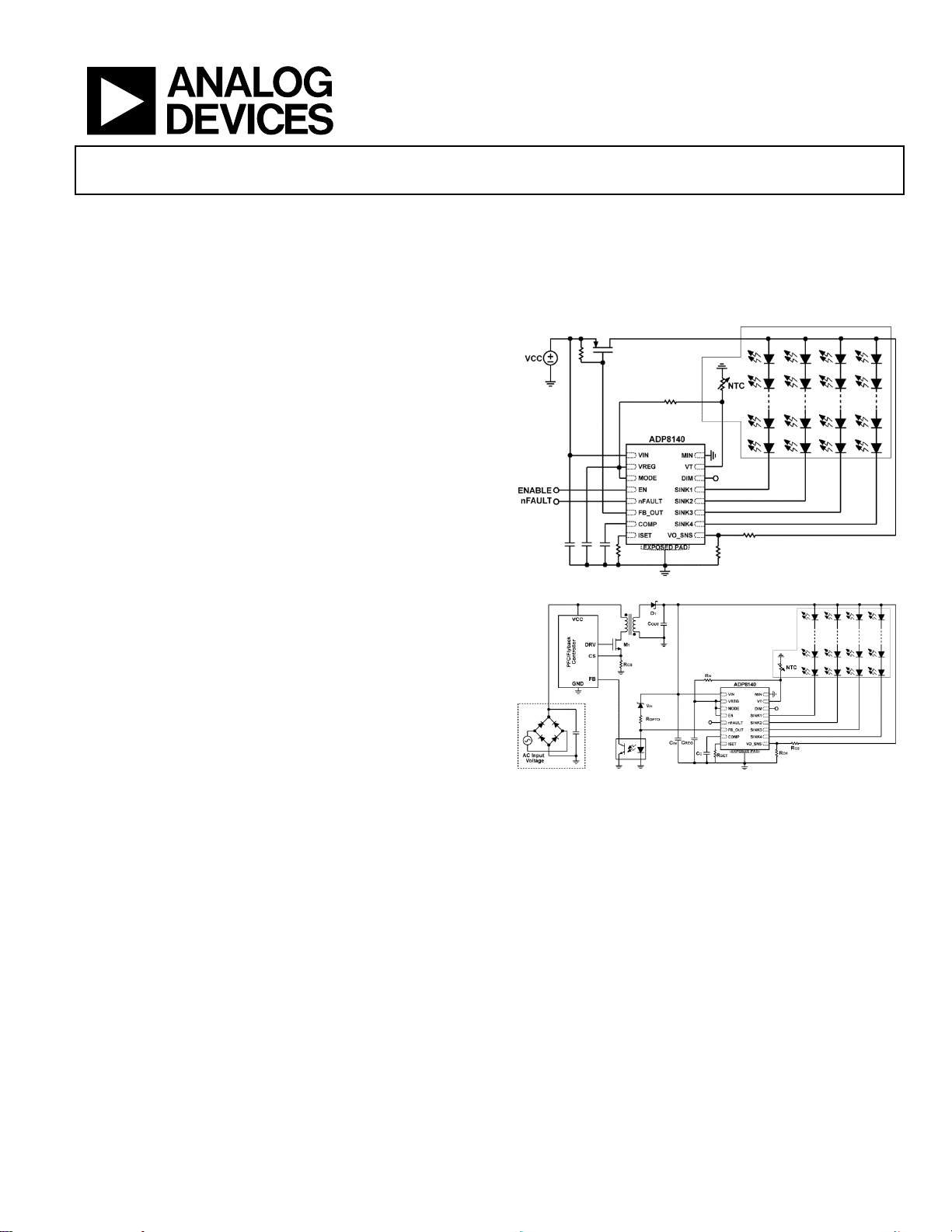
Figure 1. ADP8140 used with Shunt Regulator
Figure 2. ADP8140 used as Secondary Side Controller
events, short circuits, overvoltages, and LED open circuits.
Multiple ADP8140 ICs are easily connected in parallel to drive
additional LED strings, or higher current LEDs. The ADP8140
is available in a small, thermally enhanced, LFCSP (lead frame
chip scale package).
Rev. PrA
Information furnished by Analog Devices is believed to be accurate and reliable. However, no
responsibility is assumed by Analog Devices for its use, nor for any infringements of patents or other
rights of third parties that may result from its use. Specifications subject to change without notice. No
license is granted by implication or otherwise under any patent or patent rights of Analog Devices.
Trademarks and registered trademarks are the property of their respective owners.
One Technology Way, P.O. Box 9106, Norwood, MA 02062-9106, U.S.A.
Tel: 781.329.4700 www.analog.com
Fax: 781.461.3113 © 2012 Analog Devices, Inc. All rights reserved.
Page 2

ADP8140 Preliminary Technical Data
TABLE OF CONTENTS
Features .............................................................................................. 1
Applications ....................................................................................... 1
Typical Operating CircuitS .............................................................. 1
General Description ......................................................................... 1
Revision History .......................... Error! Bookmark not defined.
Specifications ..................................................................................... 3
Absolute Maximum Ratings ............................................................ 6
Maximum Temperature Ranges ................................................. 6
Thermal Resistance ...................................................................... 6
ESD Caution .................................................................................. 6
Pin Configurations and Function Descriptions ........................... 7
Theory of Operation ........................................................................ 8
Current Sinks ................................................................................ 9
Power Control Operation ............................................................ 9
MODE Pin Operation .................................................................. 9
Error Amplifier Power Control .................................................. 9
Low gain Buffer Power Control .................................................. 9
Using Multiple ADP8140 ICs ................................................... 10
Reducing the LED Current with the DIM Pin ....................... 10
Implementing LED Thermal Protection ................................. 10
Effect of LED Vf Mismatch ....................................................... 11
Managing the ADP8140’s Power Dissipation ......................... 12
ADP8140 Fault Protections ...................................................... 13
Startup Sequence ........................................................................ 13
Die Temperature Protection ..................................................... 14
Overvoltage Protection .............................................................. 14
Operating the ADP8140 From Higher Input Voltages ......... 14
Layout Guidelines....................................................................... 15
ADP8140 + 24 Vdc Input .......................................................... 16
ADP8140 Secondary Side Control Design example .............. 16
ADP8140 and 24Vdc Rail Design Example ............................ 17
Multiple ADP8140s With a 24Vdc Rail Design Example ..... 17
Outline Dimensions ....................................................................... 18
Ordering Guide ............................................................................... 18
Rev. PrA | Page 2 of 18
Page 3

ADP8140 Preliminary Technical Data
SPECIFICATIONS
VIN = 12 V, EN=3.0V. Typical values are at TJ = 25°C and are not guaranteed. Minimum and maximum limits are guaranteed from TJ =
−40°C to +125°C, unless otherwise noted.
Table 1.
Parameter Symbol Test Conditions/Comments Min Typ Max Unit
SUPPLY
Input Voltage
Operating Range VIN 7.5 30.0 V
Undervoltage Lockout V
UVLO Hysteresis V
Quiescent Current IQ
During Standby I
During Operation I
During Operation I
During Operation I
REG Output
REG Output Voltage VREG VIN=7.5, 12, 24 V, IREG=1 mA 2.85 3.0 3.15 V
REG Source Current IREG VIN=7.5, 12, 24 V 15 mA
REG Load Regulation VREG1 VIN=7.5, 12, 24 V, IREG=0.1 mA to 15
FEEDBACK OUTPUT
FB_OUT EA Accuracy VEA 430 450 470 mV
FB_OUT NMOS Pulldown FB_PD SINKx=0V, FB_OUT = 5.0V 12.0 15.0 18.0 mA
FB_OUT Fault Current FB_FC Fault activated, FB_OUT = 3.0 V. TBD 1 µA
Amplifier transconductance COMPgm TBD 50 TBD µmho
Transconductance amplifier
output sink/source current
Transconductance amplifier
output sink/source current
Transconductance amplifier
output resistance
Low gain EA Gbuff Gain in buffer mode
Low gain BW Low gain buffer mode 100 kHz
ISET
ISET Accuracy 500mA ILED
ISET Accuracy 350mA ILED
ISET Accuracy 100mA ILED
ISET shorted current ISET = GND TBD 570 TBD mA
ISET open current ISET = OPEN 13 TBD mA
CURRENT SINKS
Current sink headroom
voltage at max current
Sink matching at max current I
7.3 7.5 V
UVLO
150 mV
UVLO_HYS
EN = 0 V, all SINKx Zener clamps and
Q(STBY)
TBD 250 A
VREG remain active, IREG=0µA
EN = 3 V, VIN=7.5 V TBD 8.0 mA
Q(ACTIVE1)
EN = 3 V, VIN=12 V TBD 8.0 mA
Q(ACTIVE2)
EN = 3 V, VIN=28 V TBD 8.0 mA
Q(ACTIVE3)
TBD TBD V/mA
mA
COMP
COMP
COMP pin output source current TBD 500 TBD µA
SOURCE
COMP pin output sink current TBD 2.0 TBD mA
SINK
COMPRO 20 MΩ
-5% 4.0 +5%
Gbuff=Vcomp/MIN(Vsinkx)
RSET=5.11 kΩ, SINK
500
RSET=7.32 kΩ, SINK
350
RSET=25.5 kΩ, SINK
100
V
ILED = 95% * ILED
HR_500
Matching = (MAX ISINK – MIN
MATCH1
=450mV -5% 500 +5% mA
1:4
=450mV -5% 350 +5% mA
1:4
=450mV -5% 100 +5% mA
1:4
VEA
500
mV
MIN
TBD 2 %
ISINK)/(MAX ISINK + MIN ISINK)*100
Rev. PrA | Page 3 of 18
Page 4

ADP8140 Preliminary Technical Data
Parameter Symbol Test Conditions/Comments Min Typ Max Unit
Sink matching at mid current I
SINKx leakage current I
Channel Overvoltage
Threshold
Channel Overvoltage
Hysteresis
Channel Clamp (low) Current
Channel Clamp (high)
Threshold
Channel Clamp (high)
Hysteresis
Channel Clamp (high)
Current
INPUT CONTROLS
Input Threshold (low) VIL EN 0.5 V
Input Threshold (high) VIH EN 1.2 V
EN input resistance REN EN=1.2 V 400 k Ω
Mode pin pullup current IM 0V<Vmode<Vreg 18 20 22 µA
Mode Threshold 1 30.1k VM1 Threshold for increasing mode voltage
Mode Threshold 2 49.9k VM2 Threshold for increasing mode voltage
Mode Threshold 3 VM3 Threshold for increasing mode voltage
LED Scaling Controls
DIM and VT limit voltage VT
Dimming Accuracy VT = 1 V, ILED=350 mA.
DIM pin Frequency Range 140 Hz 40 kHz
MIN comparator hysteresis VMIN
THERMAL FOLDBACK (internal)
Thermal Foldback Threshold TFB
Thermal Shutdown
Hysteresis
FAU LT D ETEC T I O N
Fault Threshold FAULT
VO_SNS Hysteresis VOSNS
Fault Threshold FAULT
Fault Hysteresis FAULT
Fault Filter t
V
bias current I
O_SNS
Matching = (MAX ISINK – MIN
MATCH2
TBD 2 %
ISINK)/(MAX ISINK + MIN ISINK)*100
SINKx pin = 4V. 100 TBD µA
SINK(LKG)
CH
Threshold on SINKx to trigger CH_OVP
CLMP_LO
TBD 5.5 TBD V
fault and Channel Clamp (low)
CH
I
CLMP_LO
CH
Hysteresis after CH
CLMP_HYS
is triggered. TBD 1.0 TBD V
CLMP_LO
Channel pulldown current when
SINKx> CH
Threshold on SINKx to trigger Channel
CLMP_HI
CLMP_LO
-20% ISET +20% mA
13.5 15.0 16.5 V
Clamp (high)
CH
I
CLMP_HI
Hysteresis after CH
CLMP_HYS
is triggered. TBD 2.8 TBD V
CLMP_HI
Channel pulldown current when
SINKx> CH
CLMP_HI
-20% 510 +20% mA
TBD 0.45 TBD V
to enter DC Buffer operation.
TBD 0.75 TBD V
to enter PWM Buffer operation.
TBD 1.25 TBD V
to enter PWM EA operation.
VT (and DIM if MODE=GND) voltage to
LIMIT
TBD 2.0 TBD V
produce 100% Iout
TBD 175 TBD mA
DIM=1V, MODE=GND, ILED=350mA.
DIM=50%, 32kHz, MODE=VREG.
70 mV
HYS
TBD 130 TBD °C
THRES
TSD
TBD 20 TBD °C
HYS
Threshold for VO_SNS comparator -2% 1.2 +2% V
THRESH
Hysteresis for VO_SNS comparator 50 mV
HYS
Threshold for nFAULT comparator -5% 1.2 +5% V
THRESH
Hysteresis for nFAULT comparator 100 mV
HYS
Vo_sns and nFAULT shutdown noise
FAULT
10 Us
filter
0 TBD µA
VOSNS
Rev. PrA | Page 4 of 18
Page 5

ADP8140 Preliminary Technical Data
Parameter Symbol Test Conditions/Comments Min Typ Max Unit
nFAULT pulldown nFAULTPD Fault activated, nFAULT=0.5V TBD 3.0 TBD mA
SINK Fault Threshold SFD
Threshold to remove a sink from the
THRESH
FB loop after a CH_OVP or VOUT_OVP
fault
TBD 75 100 mV
Rev. PrA | Page 5 of 18
Page 6
ADP8140 Preliminary Technical Data
ABSOLUTE MAXIMUM RATINGS
Table 2.
Parameter Rating
VIN, FB_OUT to GND −0.3 V to +31 V
SINK1,2,3,4 to GND −0.3 V to +21 V
VREG, COMP, ISET, VMIN to GND −0.3 V to +3.6 V
DIM, VT to GND −0.3 V to +5.0 V
All other pins to GND −0.3 V to +6.0 V
Operating Ambient Temperature Range –40°C to +105°C1
Operating Junction Temperature Range –40°C to +125°C
Maximum Junction Temperature 150°C
Storage Temperature Range –45°C to +150°C
Soldering Conditions JEDEC J-STD-020
ESD (Electrostatic Discharge)
Human Body Model (HBM) ± 2.0 kV
Machine Model (MM) ± TBD V
Charged Device Model (CDM) ± TBD kV
1
The maximum operating junction temperature (T
maximum operating ambient temperature (T
Temperature Ranges section for more information.
) supersedes the
J(MAX)
). See the Maximum
A(MAX)
Stresses above those listed under Absolute Maximum Ratings
may cause permanent damage to the device. This is a stress
rating only; functional operation of the device at these or any
other conditions above those indicated in the operational
section of this specification is not implied. Exposure to absolute
maximum rating conditions for extended periods may affect
device reliability.
Absolute maximum ratings apply individually only, not in
combination. Unless otherwise specified, all voltages are
referenced to GND.
THERMAL RESISTANCE
θJA (junction to air) is specified for the worst-case conditions,
that is, a device soldered in a circuit board for surface-mount
packages. The θ
and θJC (junction to case) are determined
JA
according to JESD51-9 on a 4-layer printed circuit board (PCB)
with natural convection cooling. The LFCSP exposed pad must
be soldered to GND.
Table 3. Thermal Resistance
Package Type θJA θJB θ
Unit
JC
LFCSP 33.2 12.4 2.4 °C/W
ESD CAUTION
MAXIMUM TEMPERATURE RANGES
The maximum operating junction temperature (T
supersedes the maximum operating ambient temperature
(T
). Therefore, in situations where the ADP8866 is
A(MAX)
exposed to poor thermal resistance and a high power
dissipation (P
), the maximum ambient temperature may need
D
to be derated. In these cases, the ambient temperature
maximum can be calculated with the following equation:
T
A(MAX)
= T
J(MAX)
− (θJA × P
D(MAX)
).
J(MAX)
)
Rev. PrA | Page 6 of 18
Page 7

ADP8140 Preliminary Technical Data
PIN CONFIGURATIONS AND FUNCTION DESCRIPTIONS
Figure 3. LFCSP Pin Configuration
Table 4. Pin Function Descriptions
Pin
Mnemonic Description
No.
1 Vin Supply voltage input (7.5 V to 30 V).
2 VREG Regulated 3.0 V (typ) source. Connect a 2.2 uF capacitor from REG to ground.
3 MODE If MODE = GND, then then the part is placed into DC EA operation.
If MODE=VREG, then the part is placed into PWM EA operation.
If MODE=30.1 kΩ resistor to GND, then the part is placed into DC Low Gain Buffer operation.
If MODE=49.9 kΩ resistor to GND, then the part is placed into PWM Low Gain Buffer operation.
Never leave the MODE pin floating. See the MODE Section for more information.
4 EN Enable input. Pull high (above V
(typical) resistor.
5 nFAULT Fault output. This pin must be connected to an external pullup resistor. If using multiple ADP8140
ICs in parallel, all the nFAULT pins must be connected together.
6 FB_OUT Control signal for external power stage. The action of this pin depends on the MODE setting.
7 COMP Control signal for external power stage. The action of this pin depends on the MODE setting.
8 ISET Connect a resistor to ground to set the output current. If left floating, the current sinks are set to 14
mA.
9 VO_SNS Power stage output voltage sensing input. Connect this pin through a resistor divider to the top of
the LED strings.
10 SINK4 Current sink for LED channel 4.
11 SINK3 Current sink for LED channel 3.
12 SINK2 Current sink for LED channel 2.
13 SINK1 Current sink for LED channel 1.
14 DIM DIM input. This pin takes a PWM or DC voltage and reduces or PWM’s the output current. The
action of this pin depends on the MODE setting.
15 VT Analog current reduction pin. Typically connected to a thermister to reduce the LED output current
as the temperature increases.
16 MIN Sets the minimum voltage threshold for the VT pin. VT voltages below the MIN voltage will turn the
LEDs off
EPAD GND Ground. Connect the exposed paddle of the LFCSP to GND.
) to enable the part. EN is internally pulled low with a 400 kΩ
IH(MIN)
Rev. PrA | Page 7 of 18
Page 8

ADP8140 Preliminary Technical Data
THEORY OF OPERATION
The ADP8140 provides high current control of up to four LED
channels. Each driver can sink up to 500 mA. One external
resistor programs the sink current for all four channels. The
device features a feedback output that controls an external
power supply for optimal efficiency. The ADP8140 also
protects the LEDs, power supply, and itself against thermal
events, short circuits, and LED open circuits. Multiple
ADP8140 ICs are easily connected in parallel to drive additional
LED strings, or higher current LEDs.
Figure 4. Detailed Block Diagram
Rev. PrA | Page 8 of 18
Page 9

ADP8140 Preliminary Technical Data
CURRENT SINKS
The ADP8140 contains four internal current sinks. Each
current sink is capable of delivering 0-500 mA. To ensure
accurate regulation the voltage on the current sinks must be
greater than their maximum headroom voltage given in Table 1.
This headroom voltage varies somewhat with input voltage and
LED output current. The current is set with an external
resistor, Rset, using the following equation:
RsetkΩ
Several sinks can be combined together for higher currents per
string. For example, two sinks can be shorted together to give 2
strings, each at 1 A. Or four sinks combined to give one string
at up to 2.0 A.
Each current sink has a maximum rated voltage of 20V.
However, the maximum output voltage driving all the current
sinks, through the LEDs, is allowed to exceed 20 V. Therefore,
the ADP8140 can be safely used in conjunction with power
supplies that produce over 100 V for their output. An example
is provided at the end of this document.
(eq 1)
indicates that less power is required for the LEDs. This
operation makes the FB_OUT ideal for any power control
application that does not normally have an error amplifier. The
two primary applications for this are:
1. Controlling an optocoupler on the secondary side of
an isolated power supply
2. Controlling a PMOS transistor to regulate power in a
fixed output voltage supply.
POWER CONTROL OPERATION
The ADP8140 controls a power stage with its COMP and
FB_OUT pins. This allows the IC to optimize the efficiency
and protection of the LEDs. There are two power control
modes that the ADP8140 operates in: Error Amplifier and Low
Gain Buffer. The MODE pin is used to select the power control
mode.
MODE PIN OPERATION
The MODE pin is used to set one of four possible modes of
operation. The condition of the MODE pin effects the DIM pin
input (see “Reducing the LED Current with the DIM” Pin
section) and the power mode (see “Power Control Operation”)
MODE DIM Pin Mode Power Control
GND
30.1 k to GND
49.9 k to GND
VREG
Analog Voltage Error Amplifier
Analog Voltage Low Gain Buffer
PWM Signal Low Gain Buffer
PWM Signal Error Amplifier
ERROR AMPLIFIER POWER CONTROL
In the Error Amplifier Power Control mode, the ADP8140
takes the minimum voltage of the 4 current sinks and applies it
to the inverting input of an internal error amplifier. The output
of this error amplifier connects to the FB_OUT inverting buffer.
The FB_OUT pin outputs a current which indicates power
control. A higher FB_OUT sink current indicates that more
power is required to the LEDs. A lower FB_OUT sink current
Rev. PrA | Page 9 of 18
Figure 5. Error Amplifier Power Control
Depending on the power stage used, an RC network will need
to be connected to the COMP pin. The COMP pin connects to
the output of the FB_OUT transconductance amplifier. The
gain of this amplifier is:
∙∙
1∙∙
1∙∙
Placing a capacitor from COMP to ground adds a pole to the
control loop according to:
2∙∙
1
Placing a resistor in series with that capacitor adds a pole and a
zero.
2∙∙
1
where COMP
and COMPgm are given in Table 1
RO
General values and configurations are available for most setups
using the Error Amplifier power control can be seen in the
Applications section of this document.
LOW GAIN BUFFER POWER CONTROL
In the Low Gain Buffer Power Control mode, the ADP8140
takes the minimum voltage of the 4 current sinks, multiplies
that by Gbuff (4.0 typ, see Table 1) and outputs it to the COMP
pin. The COMP pin can then be connected to the input of a
switched mode power supply controller (SMPS). This mode is
Page 10

ADP8140 Preliminary Technical Data
useful for connecting the ADP8140 to power stages that already
have their own error amplifier. The bandwidth of the low gain
buffer is 100kHz (typ), therefore the SMPS IC’s compensation
should be set to give a total loop crossover frequency below this.
Figure 6. Low Gain Buffer Power Control
A voltage of 4.0 * 0.45 V = 1.8V will appear on the COMP pin
when the system is in steady state operation. This 1.8V must be
divided down to match the error amplifier reference of the
SMPS IC. Typically this reference is 1.2 V or 600mV.
In this mode, it is important to connect the nFAULT pin to the
EN of the SMPS IC. This will ensure that the power delivery is
immediately shutdown in the event of a fault. The FB_OUT pin
can be left floating or connected to GND. It should not be tied
to COMP or any other pin.
General values and configurations are available for most setups
using the Low Gain Buffer power control can be seen in the
Applications section of this document.
USING MULTIPLE ADP8140 ICS
Multiple ADP8140 ICs can be combined in parallel to control
the same supply. This is advantageous to control more than 4
strings of LEDs or to drive higher currents. For example, using
two ADP8140 ICs, four LED strings can be driven at 1000 mA
each. Or two strings can be driven at 2.0 A each.
When using multiple ADP8140 ICs in parallel to control one
power supply, all of the nFAULT pins must be connected
together. If any nFAULT pin goes low, all ADP8140 ICs
respond to the event. Most applications will work best if the EN
and DIM pins are also connected amongst the ADP8140 ICs,
though it is not required. The VT pins may also be connected
together, or separate NTC sensors can be used for each
ADP8140.
REDUCING THE LED CURRENT WITH THE DIM PIN
The DIM pin can reduce the output current with either an
analog voltage or a PWM signal. The ADP8140’s response to
the DIM pin depends on the condition of the MODE pin.
If MODE pin voltage is below 0.7V, then the DIM pin
functions as an analog voltage input. A DIM voltage of 2V, or
greater, does not impact the output current. A DIM voltage of
0V, reduces the output current to 0 mA. Any DIM voltage
between 2V and 0V will linearly scale the output current.
Figure 8. Reducing the output current by applying an analog voltage to the
DIM pin.
If MODE is set to a voltage greater than 0.7V, then a PWM
duty cycle applied to the DIM pin is internally filtered and used
to scale the output currents.
Figure 7. Multiple ADP8140 ICs powered off of one supply (Low Gain Buffer
Control shown).
Rev. PrA | Page 10 of 18
Figure 9. Reducing the average output current by pulse width modulating
the current sinks with the DIM pin.
IMPLEMENTING LED THERMAL PROTECTION
The ADP8140 controller has a VT pin which can be connected
to an external NTC (negative temperature coefficient) resistor.
This NTC is typically placed on the LED heat sink. Selecting
the value of the NTC and the resistor in the network shapes the
slope of the VT voltage in response to the LED temperature.
VT voltages above 2V produce no reduction in output current.
Page 11

ADP8140 Preliminary Technical Data
Below 2V, the output current is reduced 1% per 20 mV. The
LED channels are set to 0 mA when the voltage on the VT pin
is below the voltage on the MIN pin. If the VT pin voltage rises
above the MIN threshold, plus some hysteresis, then the
current sinks are re-enabled at their current set by the VT pin.
Figure 10. Using an external NTC to implement LED thermal protection.
In place of an NTC resistor, a light sensor can be used on the
VT pin. This will dim or brighten the LEDs in response to the
lighting conditions.
temperature should be relatively consistent. Given a Vf
distribution, the maximum voltage that will appear on any of
the SINK pins can be statistically calculated. For example,
suppose a mean Vf of 3.5 V and a normal distribution with a
standard deviation of 70 mV (This gives a Vf spread of 3.2 to
3.8 V -- much larger than is normally seen within one lot of
LEDs). A statistical analysis of such a distribution reveals the
following graph of the maximum voltage that may appear on
any of the SINK pins:
Figure 12. Statistical analysis of the voltage on the SINKx Pins given a
normal distribution of Vfs with a standard deviation of 70 mV . Note, the Max
value is the average plus 6 standard deviations of the distribution.
Figure 11. Using a light sensor to dim the LEDs with increasing light
intensity.
EFFECT OF LED VF MISMATCH
The forward voltage (Vf) of each LED varies from unit to unit.
In general, LEDs within the same wafer lot will have a normal
distribution with a standard deviation of about 20 mV. The
electrical specification for Vf given in the LED’s datasheet will
always be much wider than this. It is sometimes necessary to
consult the LED’s manufacturer directly for a more realistic
gauge of the Vf’s variation. Using the information on the Vf
variation, we can calculate two very important parameters in
any multi string LED design:
1. The maximum current sink voltage
2. The maximum current sink power dissipation
The ADP8140 always controls the FB_OUT pin to regulate the
output voltage to provide the minimum amount of headroom
voltage on the current sinks. One of the current sinks will be
regulated to V
three SINK pins will vary based on the distribution of Vfs. For
a given lot of LEDs, the Vf and the change in Vf with
(typ 450 mV). The voltage seen on the other
REFEA
Note that even with 30 LEDs per channel, the average and
maximum (average plus six standard deviations) SINKx
voltages remain relatively small. The value is well below the
ADP8140’s threshold for shorted LED protection (see the
Channel OVP information in the Overvoltage Protection
section below).
The second item impacted by the LED Vf variation, the
maximum current sink power dissipation, derives directly from
the voltages present at each current sink. Specifically, the
ADP8140’s power dissipation can be represented as:
Pdiss = (V
SINK1
+ V
SINK2
+ V
SINK3
+ V
SINK4
) * ILED
Again, a statistical analysis based on the LED’s Vf distribution
can be performed to predict the total power dissipation within
the ADP8140. For the same distribution used above and an
LED current of 350 mA, the following graph gives the average
and maximum power dissipations:
Rev. PrA | Page 11 of 18
Page 12

ADP8140 Preliminary Technical Data
Figure 13. Statistical analysis of the total (all 4 strings) power dissipation
for a normal distribution of Vfs with a standard deviation of 70 mV and an
LED current of 350 mA . Note, the Max value is the average plus 6 standard
MANAGING THE ADP8140’S POWER DISSIPATION
Now that the predicted power dissipation is known, the next
step is to determine if the ADP8140’s package is able to
adequately dissipate that power. The maximum power that the
ADP8140 is able to dissipate is found by following this
procedure:
Maximum ADP8140 Tj (before entering thermal foldback) =
130°C
Maximum Board Temperature = 85°C
Psi_Jb = 12.4 °C/W (Given in Table TBD)
Assume 100% of the power dissipates through the exposed pad
to the board.
Max Pdiss = (Tj – Tboard) / Psi_Jb
= (130 – 85) / 12.4 = 3.6 W
For high power dissipations (Pdiss) it is imperative to follow
the layout guidelines given in the Layout Guidelines section.
deviations of the distribution.
Rev. PrA | Page 12 of 18
Page 13

ADP8140 Preliminary Technical Data
ADP8140 FAULT PROTECTIONS
To ensure the safety of the LEDs, the ADP8140 IC, and the
power source, the ADP8140 includes a comprehensive array of
detection and protection features. These include:
- Power supply overvoltage protection
- LED Over temperature protection
- LED Short protection
- LED Open protection
- IC Over temperature protection
- Shorted ISET protection
- Open ISET and EN protection
The features are summarized on the flow chart of Figure 14.
Figure 14. ADP8140 Fault Flow Chart
STARTUP SEQUENCE
To start the ADP8140 VIN must be applied in excess of the
UVLO threshold and the EN pin must be high. However, even
with EN low, the VREG pin produces a constant 3.0V on its
output. VREG can be used as a low current supply, as needed.
Rev. PrA | Page 13 of 18
In this operation, with EN low, the ADP8140 consumes no
more than 250 μA.
When EN also goes high, then the sinks startup. There is an 8
ms delay, a time necessary for the DIM mode to determine the
PWM state of its input. When the sinks are enabled, the
Page 14

ADP8140 Preliminary Technical Data
nFAULT pin is released and the COMP and FB_OUT pins
begin their normal regulation. When EN goes low, the SINK
pins are left on for another 100us to bleed off any voltage from
the power stage. The part then enters low current consumption
operation.
Figure 15. Startup timing and signals
DIE TEMPERATURE PROTECTION
As explained above, a higher voltage on the ADP8140’s sink
pins creates a higher power dissipation within the ADP8140. If
this increase in power dissipation causes the die temperature on
the ADP8140 to rise above 130°C (typ), then the IC
automatically begins to reduce the output current on all four
sinks. If the die temperature continues to rise, then the
ADP8140 shuts down all the current sinks and releases the
pulldown on the FB_OUT pin. When the temperature drops
below 130°C, the ADP8140 restarts. If the fault or high power
dissipation persists, then the sequence repeats.
OVERVOLTAGE PROTECTION
An LED open circuit can result from a bad solder connection
or damaged LED. An open LED string results in the current
sink headroom falling to a very low level. The feedback loop
naturally interprets this as a request for more power, and so the
FB_OUT current is increased. This can quickly lead to a case
where the output voltage is too high. This increase in output
voltage is detected by either the VO_SNS pin or the SINKx
pins.
The VO_SNS pin senses the output voltage of the power supply
through an external resistor divider. VO_SNS is then
compared to an internal threshold (1.2 V typical). If the
output voltage rises such that the VO_SNS pin is greater than
1.2 V, then an output overvoltage fault (VOUT_OVP) is
declared. During a VOUT_OVP fault, the FB_OUT pulldown
NMOS is released, causing the power stage to shutdown. The
LED current sinks are left enabled during this event. When
VO_SNS drops to 1.15 V (typical), the FB_OUT function
resumes its normal operation.
Alternatively, the output voltage may not rise high enough to
trigger VO_SNS, but it may rise high enough to cause one of
the SINKx pins to exceed 5.0V (typical). Or a shorted LED may
cause the SINKx pins to exceed this level. To prevent excessive
power dissipation and damage to the IC, when a SINKx pin
rises above 5.0 V, a channel over voltage (CH_OVP) fault is
declared. During a CH_OVP fault, the FB_OUT pulldown
NMOS is released, causing the power stage to shutdown. The
LED current sinks are left enabled during this event. When the
SINKx voltage drops to 5.0 V (typical), the FB_OUT function
resumes its normal operation.
Continued output overvoltage operation degrades efficiency
and can affect the lifetime of passive components. Therefore,
when an overvoltage condition is detected (either VOUT_OVP
or CH_OVP), then any open LED current sinks are identified
and removed from the feedback loop.
During a VOUT_OVP or CH_OVP event, the nFAULT pin is
pulled low. nFAULT is released high when the overvoltage
condition has ended.
OPERATING THE ADP8140 FROM HIGHER INPUT
VOLTAGES
The ADP8140 is capable of operating from an input voltage
(Vin) range of 7.5 to 30 V. However, higher voltages can be
used to power the ADP8140, as long as an appropriate current
limiting circuit is used.
It is sometimes sufficient to limit the voltage on VIN by placing
a Zener diode on VIN and limiting the current with a resistor
from the input voltage to the VIN pin. This method could be
used if standby power dissipation is not an issue.
Alternatively, if the supply voltage range is small, an additional
Zener between the supply and VIN will shift the voltage at the
VIN pin below 30 V. This method adds minimal power
dissipation in both standby and active modes.
However, a more robust voltage limiter uses a Zener, an NPN,
and two resistors. This simple circuit gives the required
operating Iq during normal operation, but also reduces the
standby current when the ADP8140 is disabled. The circuit is
shown in Figure 16.
Rev. PrA | Page 14 of 18
Page 15

ADP8140 Preliminary Technical Data
RLIM limits the maximum current during transients. A value
of a few hundred ohms is sufficient. When the ADP8140 is
active, the additional, worst case, power dissipation from this
limit circuitry is given by:
Figure 16. VIN current limiting circuit for high input voltages
VZ is selected to be below the minimum value of the ADP8140’s
active VIN clamp (given in Table 1). The VIN voltage will be
regulated to V
– 0.7 V. The resistor, RZ, should be selected to
Z
limit the current when the ADP8140 is disabled, yet still
provide enough current to reverse bias the Zener and drive the
NPN when the ADP8140 is active. The current through R
is
Z
given by:
IRZ = (Vcc – VZ) / RZ
A value of 100 μA at the minimum expected Vcc is generally
sufficient. Even at maximum Vcc, this will only contribute a
few mW of power dissipation during standby.
∆
0.7∙
48 24 0.7∙374
LAYOUT GUIDELINES
1. The exposed pad of the ADP8140 must be properly
connected to a heat sink. This includes soldered to the board
and connected to a large plane of ground metal with an array of
thermal vias.
2. The ADP8140 has been designed for easy layout with single
sided metal core substrates. If FR4 substrate used, thermal vias
must be used between the LFCSP exposed pad and a large
ground trace on the opposite side of the board.
Rev. PrA | Page 15 of 18
Page 16

ADP8140 Preliminary Technical Data
ADP8140 + 24 VDC INPUT
Figure 17.
ADP8140 SECONDARY SIDE CONTROL DESIGN EXAMPLE
Figure 18.
Rev. PrA | Page 16 of 18
Page 17

ADP8140 Preliminary Technical Data
ADP8140 AND 24VDC RAIL DESIGN EXAMPLE
Figure 19.
MULTIPLE ADP8140S WITH A 24VDC RAIL DESIGN EXAMPLE
Figure 20.
Rev. PrA | Page 17 of 18
Page 18

ADP8140 Preliminary Technical Data
OUTLINE DIMENSIONS
Figure 21. Lead Frame Chip Scale Package (LFCSP)
ORDERING GUIDE
Model1 Temperature Range Package Description Package Option
ADP8140ACPZ_TBD -40 to +125°C LFCSP, Tape and Reel LFCSP
1
Z = RoHS Compliant Part.
©
2012
Analog Devices, Inc. All rights reserved. Trademarks and
registered trademarks are the property of their respective owners.
PR10935-0-7/12(PrA)
Rev. PrA | Page 18 of 18
 Loading...