

Page 1
A
V
Keypad Decoder and I/O Expansion
FEATURES
16-element FIFO for event recording
19 configurable I/Os allowing functions such as
Keypad decoding for matrix up to 11 × 8
Key press/release interrupts
Key pad lock/unlock
GPIO functions
GPI with selectable interrupt level
100 kΩ or 300 kΩ pull-up resistors
300 kΩ pull-down resistors
GPO with push-pull or open drain
Dual programmable logic blocks
PWM generator
Internal PWM generation
External PWM with internal PWM AND function
Clock divider
Reset generators
2
I
C interface with fast-mode plus (Fm+) support up to 1 MHz
Open-drain interrupt output
24-lead LFCSP 3.5 mm × 3.5 mm
25-ball WLCSP 1.99 mm × 1.99 mm
APPLICATIONS
Devices requiring keypad entry and I/O expansion
capabilities
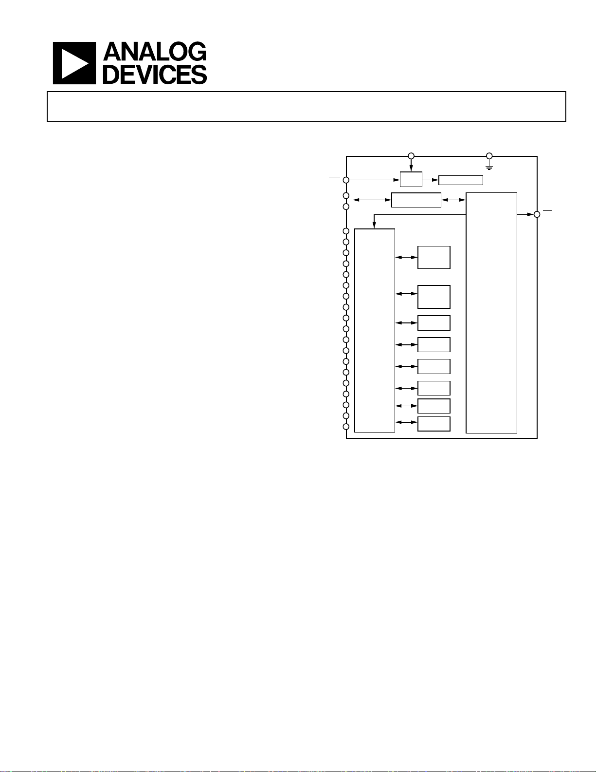
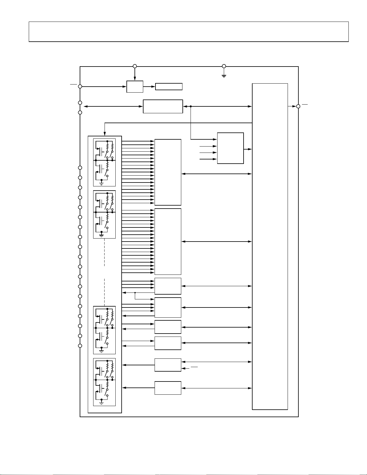
GENERAL DESCRIPTION
The ADP5589 is a 19 I/O port expander with built-in keypad
matrix decoder, programmable logic, reset generator, and
PWM generator. I/O expander ICs are used in portable devices
(phones, remote controls, and cameras) and nonportable
applications (healthcare, industrial, and instrumentation). I/O
expanders can be used to increase the number of I/Os available
to a processor or to reduce the number of I/Os required
through interface connectors for front panel designs.
The ADP5589, which handles all key scanning and decoding,
can flag the main processor via an interrupt line when new key
events have occurred. In addition, GPI changes and logic
changes can be tracked as events via the FIFO, eliminating the
ADP5589
FUNCTIONAL BLOCK DIAGRAM
DD
ADP5589
RST
SD
SCL
C10
UVLO
POR
I2C INTERFACE
R0
R1
R2
R3
R4
R5
R6
R7
C0
C1
C2
C3
C4
C5
C6
C7
C8
C9
I/O
CONFIG
KEY SCAN
AND
DECODE
GPI SCAN
AND
DECODE
LOGIC 1
LOGIC 2
CLK DIV
PWM
RESET 1
GEN
RESET 2
GEN
OSCILLAT OR
Figure 1.
need to monitor different registers for event changes. The
ADP5589 is equipped with a FIFO to store up to 16 events.
Events can be read back by the processor via an I
interface.
The ADP5589 frees up the main processor from having to
monitor the keypad, thereby reducing power consumption
and/or increasing processor bandwidth for performing other
functions.
The programmable logic functions allow common logic
requirements to be integrated as part of the GPIO expander,
saving board area and cost.
GND
REGISTERS
2
C compatible
INT
09714-001
Rev. A
Information furnished by Analog Devices is believed to be accurate and reliable. However, no
responsibility is assumed by Anal og Devices for its use, nor for any infringements of patents or ot her
rights of third parties that may result from its use. Specifications subject to change without notice. No
license is granted by implication or otherwise under any patent or patent rights of Analog Devices.
Trademarks and registered trademarks are the property of their respective owners.
One Technology Way, P.O. Box 9106, Norwood, MA 02062-9106, U.S.A.
Tel: 781.329.4700 www.analog.com
Fax: 781.461.3113 ©2011 Analog Devices, Inc. All rights reserved.
Page 2

ADP5589
TABLE OF CONTENTS
Features.............................................................................................. 1
Applications....................................................................................... 1
Functional Block Diagram .............................................................. 1
General Description ......................................................................... 1
Revision History ............................................................................... 2
Specifications..................................................................................... 3
Absolute Maximum Ratings............................................................ 5
Thermal Resistance ...................................................................... 5
ESD Caution.................................................................................. 5
Pin Configuration and Function Descriptions............................. 6
Quick Device Overview................................................................... 7
Device Enable................................................................................ 8
Device Overview .......................................................................... 8
Detailed Description ........................................................................9
Event FIFO.....................................................................................9
Key Scan Control...........................................................................9
GPO Output................................................................................ 15
Logic Blocks ................................................................................ 16
PWM Block................................................................................. 17
Clock Divider Block................................................................... 17
Reset Blocks ................................................................................ 17
Interrupts..................................................................................... 18
Register Interface............................................................................ 19
Register Map ................................................................................... 21
Detailed Register Descriptions................................................. 23
Application Diagram...................................................................... 47
Outline Dimensions....................................................................... 48
Ordering Guide .......................................................................... 48
REVISION HISTORY
8/11—Revision A: Initial Version
Rev. A | Page 2 of 48
Page 3

ADP5589
SPECIFICATIONS
VDD = 1.8 V to 3.3 V, TA = −40°C to +85C, unless otherwise noted.1
Table 1.
Parameter Symbol Test Conditions/Comments Min Typ Max Unit
SUPPLY VOLTAGE
VDD Input Voltage Range VDD 1.65 3.6 V
Undervoltage Lockout Threshold UVLO
SUPPLY CURRENT
Standby Current I
VDD = 3.3 V 1 10 µA
Operating Current (One Key Press) I
I
I
I
PULL-UP, PULL-DOWN RESISTANCE
Pull-Up Option 1 50 100 150 kΩ
Pull-Up Option 2 150 300 450 kΩ
Pull-Down 150 300 450 kΩ
INPUT LOGIC LEVEL (
R5, R6, R7, C0, C1, C2, C3, C4, C5, C6, C7, C8, C9, C10)
RST
, SCL, SDA, R0, R1, R2, R3, R4,
Logic Low Input Voltage VIL 0.3 × VDD V
Logic High Input Voltage VIH 0.7 × VDD V
Input Leakage Current (Per Pin) V
PUSH-PULL OUTPUT LOGIC LEVEL (R0, R1, R2, R3, R4,
R5, R6, R7, C0, C1, C2, C3, C4, C5, C6, C7, C8, C9, C10)
Logic Low Output Voltage2 V
Logic Low Output Voltage3 V
Logic High Output Voltage VOH Source current = 5 mA 0.7 × VDD V
Logic High Leakage Current (Per Pin) V
INT
INT
, SDA)
)
OPEN-DRAIN OUTPUT LOGIC LEVEL (
Logic Low Output Voltage (
Logic Low Output Voltage (SDA) VOL I
Logic High Leakage Current (Per Pin) V
Logic Propagation Delay 125 300 ns
FF1 Hold Time4 0 ns
FF1 Setup Time4 175 ns
FF2 Hold Time
4
FF2 Setup Time4 175 ns
GPIO Debounce4 70 µs
Internal Oscillator Frequency5 OSC
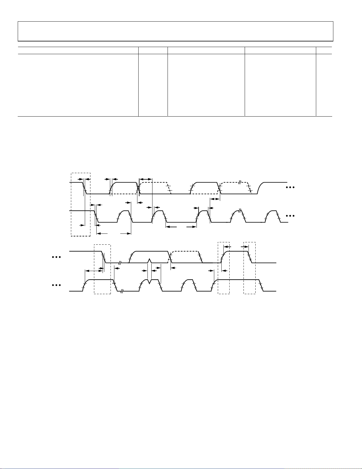
I2C TIMING SPECIFICATIONS
Delay from UVLO/Reset Inactive to I2C Access 60 µs
SCL Clock Frequency f
SCL High Time t
SCL Low Time t
Data Setup Time t
Data Hold Time t
Setup Time for Repeated Start t
UVLO active, VDD falling 1.2 1.3 V
VDD
UVLO inactive, VDD rising 1.4 1.6 V
VDD = 1.65 V 1 4 A
STNBY
CORE_FREQ = 50 kHz, scan active,
SCAN = 10 ms
30 40 µA
300 kΩ pull-up, VDD = 1.65 V
CORE_FREQ = 50 kHz, scan active,
SCAN = 10 ms
35 45 µA
100 kΩ pull-up, VDD = 1.65 V
CORE_FREQ = 50 kHz, scan active,
SCAN = 10 ms
75 85 A
300 kΩ pull-up, VDD = 3.3 V
CORE_FREQ = 50 kHz, scan active,
SCAN = 10 ms
80 90 A
100 kΩ pull-up, VDD = 3.3 V
0.1 1 µA
I-Leak
Sink current = 10 mA 0.4 V
OL
Sink current = 10 mA 0.5 V
OL
0.1 1 µA
OH-Leak
I
V
OL
0.1 1 µA
OH-Leak
= 10 mA 0.4 V
SINK
= 20 mA 0.4 V
SINK
0 ns
900 1000 1100 kHz
FREQ
0 1000 kHz
SCL
0.26 µs
HIGH
0.5 µs
LOW
50 ns
SU; DAT
0
HD; DAT
0.26 µs
SU; STA
µs
Rev. A | Page 3 of 48
Page 4
ADP5589
Parameter Symbol Test Conditions/Comments Min Typ Max Unit
Hold Time for Start/Repeated Start t
Bus Free Time for Stop and Start Condition t
Setup Time for Stop Condition t
Data Valid Time t
Data Valid Acknowledge t
Rise Time for SCL and SDA tR 120 ns
Fall Time for SCL and SDA tF 120 ns
Pulse Width of Suppressed Spike tSP 0 50 ns
Capacitive Load for Each Bus Line C
1
All limits at temperature extremes are guaranteed via correlation using standard statistical quality control (SQC). Typical values are at TA = 25°C, VDD = 1.8 V.
2
Maximum of five GPIOs active simultaneously.
3
All GPIOs active simultaneously.
4
Guaranteed by design.
5
All timers are referenced from the base oscillator and have the same ±10% accuracy.
6
CB is the total capacitance of one bus line in picofarads.
SDA
SCL
SDA
70%
30%
t
F
S
t
R
t
t
F
HD; DAT
70%
30%
t
HD; STA
f
1/
SCL
FIRST CL OCK CYCLE
70%
30%
70%
30%
0.26 µs
HD; STA
0.5 µs
BUF
0.26 µs
SU; STO
0.45 µs
VD; DAT
0.45 µs
VD; ACK
B
t
SU; DAT
6
550 pF
t
70%
30%
VD; DAT
NINTH CLOCK
t
BUF
t
t
R
70%
30%
t
LOW
HIGH
SCL
VIL = 0.3VDD
V
= 0.7VDD
IH
t
SU; STA
t
HD; STA
t
SP
Sr PS
Figure 2. I
2
C Interface Timing Diagram
70%
30%
t
VD; ACK
t
SU; STO
NINTH CLOCK
09714-002
Rev. A | Page 4 of 48
Page 5
ADP5589
ABSOLUTE MAXIMUM RATINGS
Table 2.
Parameter Rating
VDD to Ground –0.3 V to 4 V
SCL, SDA, RST, INT, R0, R1, R2,
–0.3 V to (VDD + 0.3 V)
R3, R4, R5, R6, R7, C0, C1, C2,
C3, C4, C5, C6, C7, C8, C9, C10
to Ground
1
Operating Ambient
−40°C to +85°C
Temperature Range
Operating Junction
−40°C to +125°C
Temperature Range
Storage Temperature Range −65°C to +150°C
Soldering Conditions JEDEC J-STD-020
1
In applications where high power dissipation and poor thermal resistance
are present, the maximum ambient temperature may have to be derated.
Maximum ambient temperature (T
operating junction temperature (T
dissipation of the device (P
resistance of the part/package in the application (θ
equation: T
A(MAX)
= T
J(MAXOP)
D(MAX)
− (θJA × P
) is dependent on the maximum
A(MAX)
= 125°C), the maximum power
J(MAXOP)
), and the junction-to-ambient thermal
).
D(MAX)
), using the following
JA
Stresses above those listed under Absolute Maximum Ratings
may cause permanent damage to the device. This is a stress
rating only; functional operation of the device at these or any
other conditions above those indicated in the operational
section of this specification is not implied. Exposure to absolute
maximum rating conditions for extended periods may affect
device reliability.
Absolute maximum ratings apply individually only, not in
combination. Unless otherwise specified, all other voltages are
referenced to ground.
THERMAL RESISTANCE
θJA is specified for the worst-case conditions, that is, a device
soldered in a circuit board for surface-mount packages.
Table 3.
Thermal Resistance θJA Unit
24-Lead LFCSP 43.83 C/W
Maximum Power Dissipation 120 mW
25-Ball WLCSP 43 C/W
Maximum Power Dissipation 120 mW
ESD CAUTION
Rev. A | Page 5 of 48
Page 6
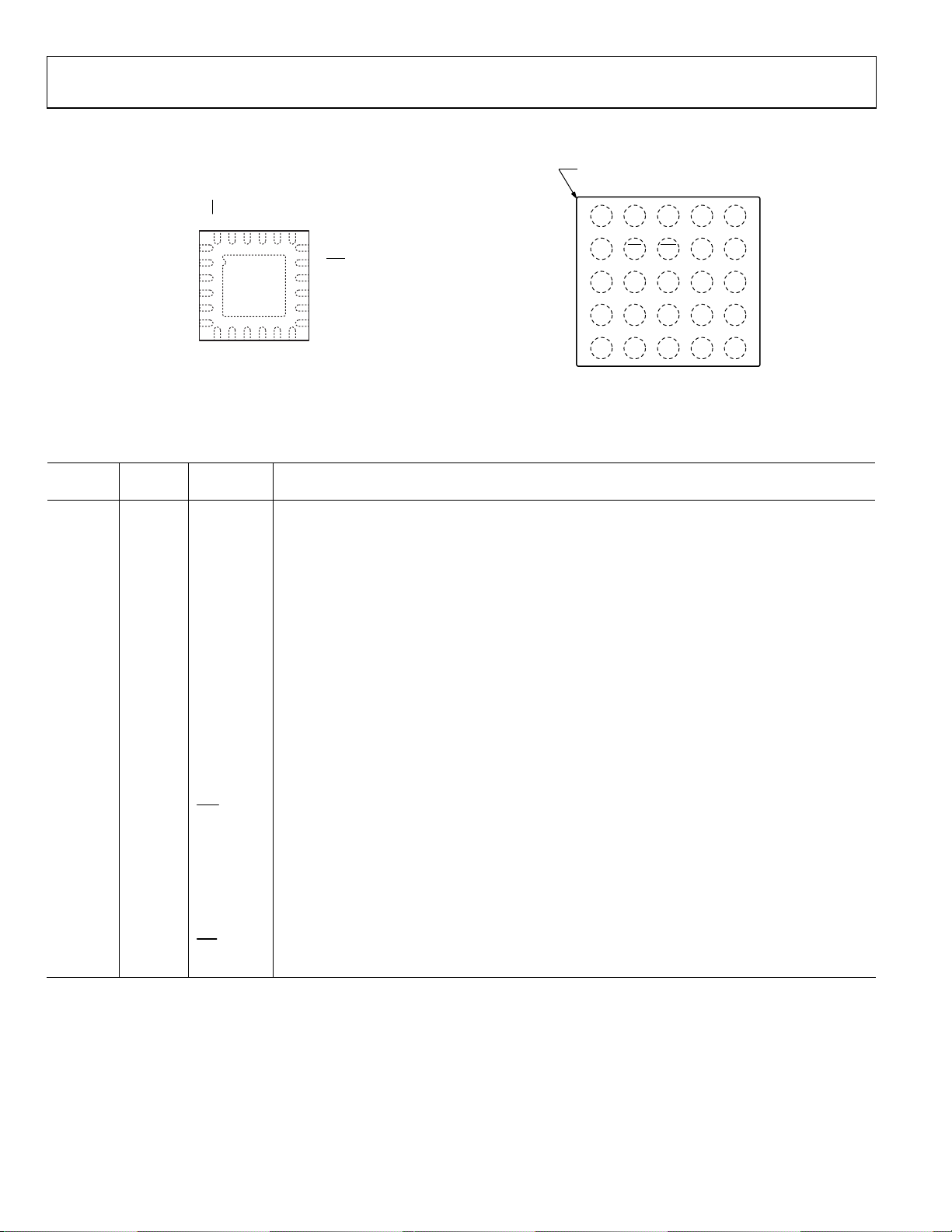
ADP5589
PIN CONFIGURATION AND FUNCTION DESCRIPTIONS
DA
INT
SCL
S
C10
C8
24
1
R7
2
R6
3
R5
R4
R3
R2
NOTES
1. THE EXPOSED
ADP5589
TOP VIEW
4
(Not to Scale)
5
6
7
R1
PAD MUST BE CONN
Figure 3. LFCSP Pin Configuration
Table 4. Pin Function Descriptions
Pin No.
(LFCSP)
Pin No.
(WLCSP) Mnemonic Description
1 E3 R7
2 E2 R6
3 E1 R5
4 D1 R4
5 D2 R3
6 C1 R2
7 C2 R1
8 B1 R0
9 B4 C0
10 C3 C1
11 C4 C2
12 D3 C3
13 D4 C4
14 E4 C5
15 E5 C6
16 D5 C7
17 B3
RST
18 A1 VDD
19 C5 C8
20 B5 C9
21 A5 C10
22 A2 SDA
23 A3 SCL
24 B2
INT
EP (pad) A4 GND
C9
23
22
21
20
19
18
VDD
ST
17
R
16
C7
15
C6
14
C5
C4
13
9
8
11
12
10
C3
C2
C1
C0
R0
ECTED
09714-003
TO GROUND.
GPIO 8. This pin functions as Row 7 if used as keypad.
GPIO 7. This pin functions as Row 6 if used as keypad.
GPIO 6. This pin functions as Row 5 if used as keypad.
GPIO 5 (GPIO alternate function: RESET1). This pin functions as Row 4 if used as keypad.
GPIO 4 (GPIO alternate function: LC1, PWM_OUT, or CLK_OUT. This pin functions as Row 3 if used as keypad.
GPIO 3 (GPIO alternate function: LB1). This pin functions as Row 2 if used as a keypad.
GPIO 2 (GPIO alternate function: LA1). This pin functions as Row 1 if used as a keypad.
GPIO 1 (GPIO alternate function: LY1). This pin functions as Row 0 if used as a keypad.
GPIO 9. This pin functions as Column 0 if used as keypad.
GPIO 10. This pin functions as Column 1 if used as keypad.
GPIO 11. This pin functions as Column 2 if used as keypad.
GPIO 12. This pin functions as Column 3 if used as keypad.
GPIO 13 (GPIO alternate function: RESET2). This pin functions as Column 4 if used as keypad.
GPIO 14. This pin functions as Column 5 if used as keypad.
GPIO 15 (GPIO alternate function: LC2, PWM_IN, or CLK_IN). This pin functions as Column 6 if used as keypad.
GPIO 16 (GPIO alternate function: LB2). This pin functions as Column 7 if used as keypad.
Input Reset Signal.
Supply Voltage Input.
GPIO 17 (GPIO alternate function: LA2). This pin functions as Column 8 if used as keypad.
GPIO 18 (GPIO alternate function: LY2). This pin functions as Column 9 if used as keypad.
GPIO 19. This pin functions as Column 10 if used as keypad.
I2C Data Input/Output.
I2C Clock Input.
Open-Drain Interrupt Output.
Ground. The exposed pad of the LFCSP package must be connected to ground.
BALLA1
CORNER
1
234
VDD SDA SCL GND C
A
R0
B
C
D
E
INT
R2 R1 C1 C2 C8
R4
R3
R5 R6 R7 C5
TOP VIEW
(BALL SI DE DOWN)
Not to Scale
C0 C9
RST
C3 C4 C7
Figure 4. WLCSP Pin Configuration
5
10
C6
09714-104
Rev. A | Page 6 of 48
Page 7
ADP5589
V
QUICK DEVICE OVERVIEW
ADP5589
RST
SDA
SCL
R0
R1
R2
R3
R4
R5
R6
R7
C0
C1
C2
C3
C4
C5
C6
C7
C8
C9
C10
I/O
CONFIGURATION
(R0)
(R1)
(R2)
(R3)
(R4)
(R5)
(R6)
(R7)
(C0)
(C1)
(C2)
(C3)
(C4)
(C5)
(C6)
(C7)
(C8)
(C9)
(C10)
(R0)
(R1)
(R2)
(R3)
(R4)
(R5)
(R6)
(R7)
(C0)
(C1)
(C2)
(C3)
(C4)
(C5)
(C6)
(C7)
(C8)
(C9)
(C10)
(R1)
(R2)
(R3)
(R0)
(C8)
(C7)
(C6)
(C9)
(C6)
(R3)
(C6)
(R3)
DD
UVLO
POR
I2C INTERFACE
ROW 0
ROW 1
ROW 2
ROW 3
ROW 4
ROW 5
ROW 6
ROW 7
COL 0
COL 1
COL 2
COL 3
COL 4
COL 5
COL 6
COL 7
COL 8
COL 9
COL 10
GPIO 1
GPIO 2
GPIO 3
GPIO 4
GPIO 5
GPIO 6
GPIO 7
GPIO 8
GPIO 9
GPIO 10
GPIO 11
GPIO 12
GPIO 13
GPIO 14
GPIO 15
GPIO 16
GPIO 17
GPIO 18
GPIO 19
LA1
LB1
LC1
LY1
LA2
LB2
LC2
LY2
CLK_IN
CLK_OUT
PWM_IN
PWM_OUT
OSCILLATOR
KEY SCAN
AND
DECODE
GPI SCAN
AND
DECODE
LOGIC 1
LOGIC 2
CLK DIV
PWM
2
C BUSY?
I
KEY EVENT
GPI EVENT
LOGIC EVENT
GND
UPDATE
INT
FIFO
REGISTERS
(R4)
RESET1
(C4)
RESET2
RESET1
GEN
RESET2
GEN
RST
9714-004
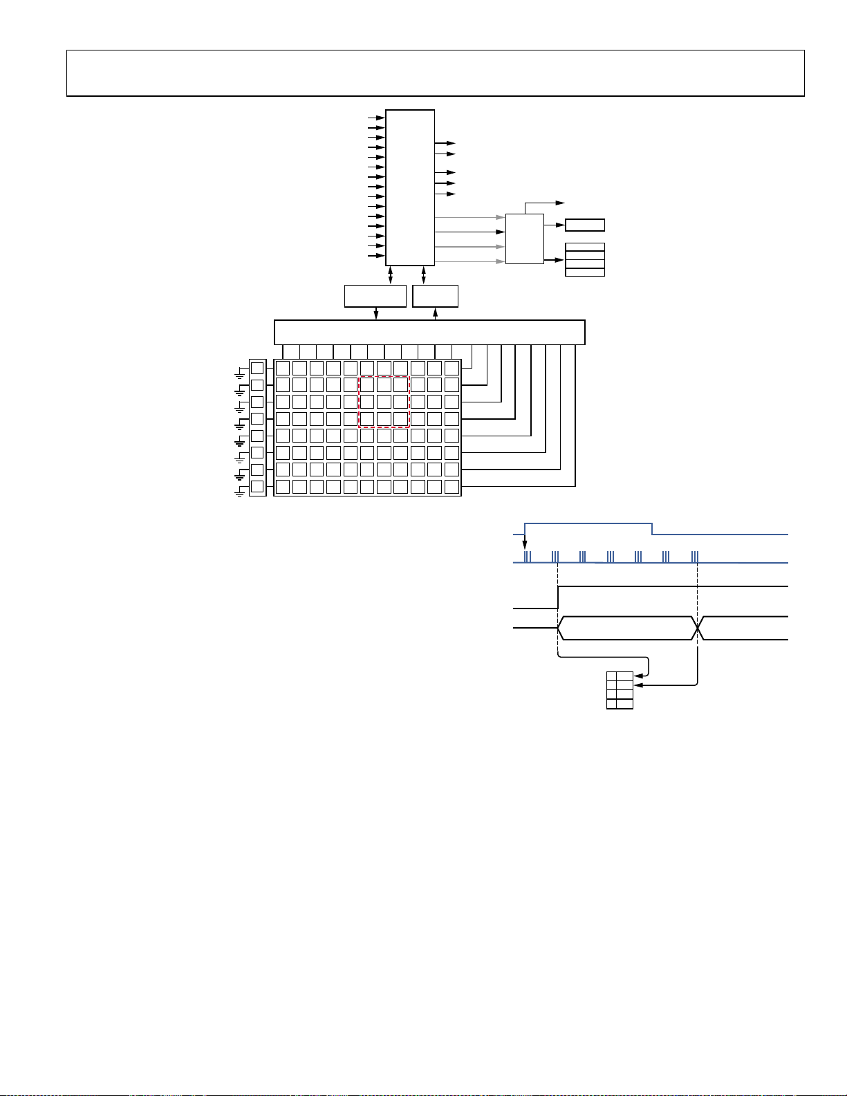
Figure 5. Internal Block Diagram
Rev. A | Page 7 of 48
Page 8
ADP5589
V
DEVICE ENABLE
I/O
RST
pin is
When sufficient voltage is applied to VDD and the
driven with a logic high level, the starts up in standby
ADP5589
mode with all settings at default. The user can configure the
device via the I
ADP5589
The
enters a reset state and all settings return to default.
RST
pin features a debounce filter.
2
C interface. When the
RST
pin is low, the
DEVICE OVERVIEW
The ADP5589 contains 19 multiconfigurable input/output pins.
Each pin can be programmed to enable the device to carry out
its various functions, as follows:
• Keypad matrix decoding (11-column by 8-row matrix
maximum).
• General-purpose I/O expansion (up to 19 inputs/outputs).
• PWM generation.
• Clock division of externally supplied source.
• Dual logic function building blocks (up to three inputs,
one output).
• Two re s et generators.
All 19 input/output pins have an I/O structure, as shown in
Figure 6.
DD
100kΩ
300kΩ
I/O
DRIVE
300kΩ
Each I/O can be pulled up with a 100 kΩ or 300 kΩ resistor or
pulled down with a 300 kΩ resistor. For logic output drive, each
I/O has a 5 mA PMOS source and a 10 mA NMOS sink for
push-pull type output. For open-drain output situations, the
5 mA PMOS source is not enabled. For logic input applications,
each I/O can be sampled directly or, alternatively, sampled
through a debounce filter.
The I/O structure shown in Figure 6 allows for all GPI and GPO
functions, as well as PWM and clock divide functions. For key
matrix scan and decode, the scanning circuit uses the 100 kΩ or
300 kΩ resistor for pulling up keypad row pins and the 10 mA
NMOS sinks for grounding keypad column pins (see the Key
Scan Control section for details about key decoding).
Configuration of the device is carried out by programming an
array of internal registers via the I
2
C interface. Feedback of
device status and pending interrupts can be flagged to an
external processor via the
INT
pin.
The ADP5589 is offered with three feature sets. Ta b le 5 lists the
options that are available for each model of the ADP5589.
Table 5. Available Options
Models Description
ADP5589ACPZ-00-R7
All GPIOs pulled up (default option)
ADP5589ACBZ-00-R7
ADP5589ACPZ-01-R7
Reset pass-through1
ADP5589ACBZ-01-R7
ADP5589ACPZ-02-R7
ADP5589ACBZ-02-R7
1
Reset pass-through implies that the RESET1 output (R4) follows the logic
level of the reset input pin,
2
Special function pins are defined as R0 (Row 0), R3 (Row 3), R4 (Row 4), C4
(Column 4), C6 (Column 6), and C9 (Column 9).
Pull-down on special function pins
RST
, after the oscillator has been enabled.
2
DEBOUNCE
Figure 6. I/O Structure
09714-005
Rev. A | Page 8 of 48
Page 9
ADP5589
DETAILED DESCRIPTION
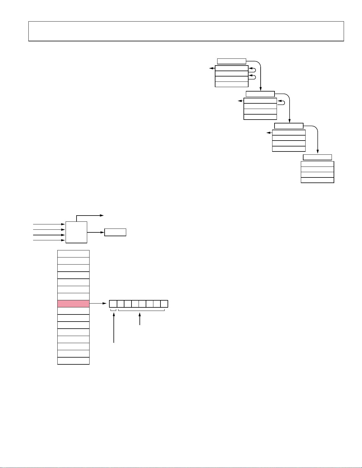
EVENT FIFO
It is important to understand the function of the event FIFO.
The ADP5589 features an event FIFO that can record as many
as 16 events. By default, the FIFO primarily records key events,
such as key press and key release. However, it is possible to
configure the general-purpose input (GPI) and logic activity
to generate event information on the FIFO as well. An event
count, EC[4:0], is composed of five bits and works in tandem
with the FIFO so that the user knows how much of the FIFO
must be read back at any given time.
The FIFO is composed of 16 eight-bit sections that the user
accesses by reading the FIFO_x registers. The actual FIFO
is not in user accessible registers until a read occurs. The
FIFO can be thought of as a “first in, first out” buffer used
to fill Register 0x03 to Register 0x12.
The event FIFO is made up of 16 eight-bit registers. In each
register, Bits[6:0] hold the event identifier, and Bit 7 holds the
event state. With seven bits, 127 different events can be identified.
See Tab le 1 1 for event decoding.
OVRFLOW_INT
KEY EVENTS
GPI EVENTS
LOGIC EVENTS
When events are available on the FIFO, the user should first
read back the event count, EC[4:0], to determine how many
events must be read back. Events can be read from the top of
the FIFO only. When an event is read back, all remaining events
in the FIFO are shifted up one location, and the EC[4:0] count
is decremented.
FIFO
UPDATE
EVENT1[7:0]
EVENT2[7:0]
EVENT3[7:0]
EVENT4[7:0]
EVENT5[7:0]
EVENT6[7:0]
EVENT7[7:0]
EVENT8[7:0]
EVENT9[7:0]
EVENT10[7:0]
EVENT11[7:0]
EVENT12[7:0]
EVENT13[7:0]
EVENT14[7:0]
EVENT15[7:0]
EVENT16[7:0]
Figure 7. Breakdown of Eventx[7:0] Bits
EC[4:0]
7
6543210
EVENT8_ID ENTIF IER[6:0]
EVENT8_STATE
FIRST
READ
The FIFO registers (0x03 to 0x12) always point to the top of the
FIFO (that is, the location of EVENT1[7:0]). If the user tries to
read back from any location in a FIFO, data is always obtained
from the top of that FIFO. This ensures that events can only be
read back in the order in which they occurred, thus ensuring
the integrity of the FIFO system.
Some of the onboard functions of ADP5589 can be programmed to generate events on the FIFO. A FIFO update control
block manages updates to the FIFO. If an I
accessing any of the FIFO address locations, updates are paused
until the I
A FIFO overflow event occurs when more than 16 events are
generated prior to an external processor reading a FIFO and
clearing it.
If an overflow condition occurs, the overflow status bit is set.
An interrupt is generated if overflow interrupt is enabled,
signaling to the processor that more than 16 events have
occurred.
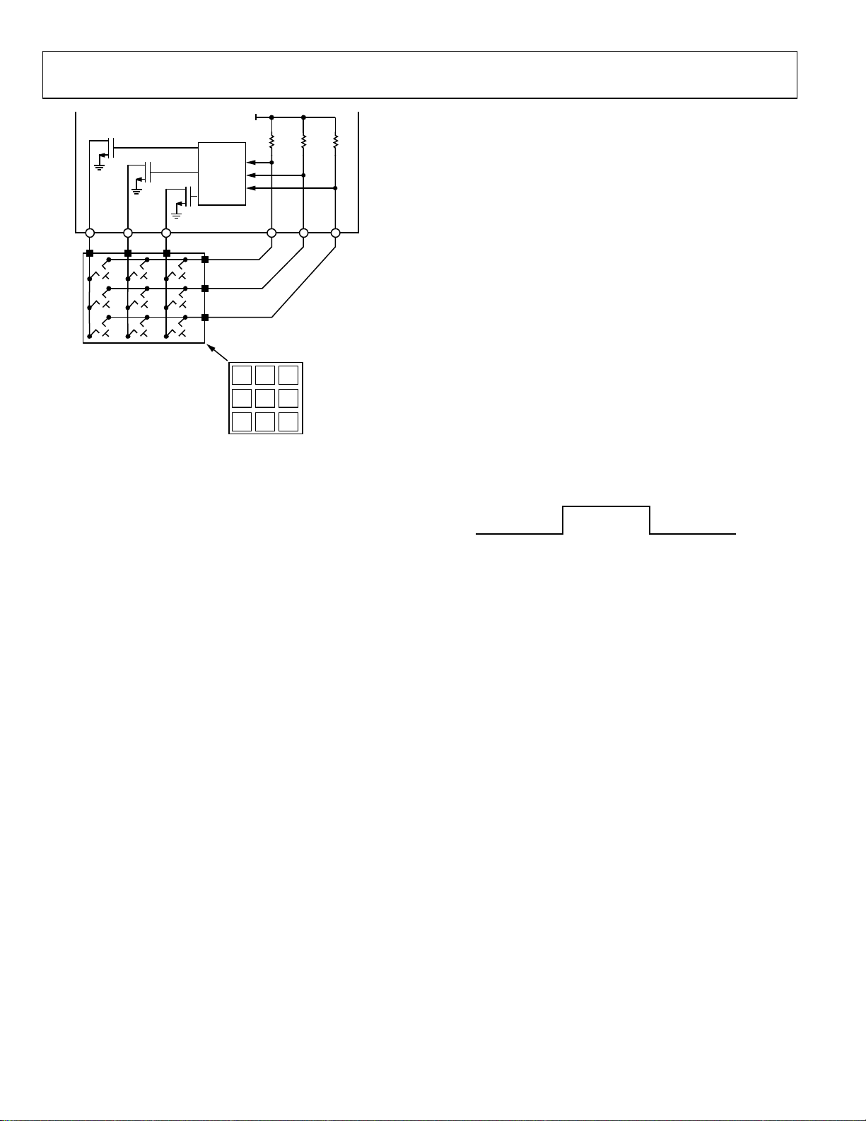
KEY SCAN CONTROL
General
The 19 input/output pins can be configured to decode a keypad
09714-006
matrix up to a maximum size of 88 switches (11 × 8 matrix).
Smaller matrices can also be configured, freeing up the unused
row and column pins for other I/O functions.
The R0 through R7 I/O pins comprise the rows of the keypad
matrix. The C0 through C10 I/O pins comprise the columns of
the keypad matrix. Pins used as rows are pulled up via the internal
300 k (or 100 k) resistors. Pins used as columns are driven
low via the internal NMOS current sink.
EC = 3
KEY 3 PRESSED
KEY 3 RELEASED
GPI 7 ACTIVE
SECOND
READ
2
C transaction has completed.
EC = 2
KEY 3 RELEASED
GPI 7 ACTIVE
THIRD
READ
Figure 8. FIFO Operation
EC = 1
GPI 7 ACTIVE
2
C transaction is
EC = 0
09714-007
Rev. A | Page 9 of 48
Page 10
ADP5589
1
23
4
56
7
89
Figure 9. Simplified Key Scan Block
VDD
KEY
SCAN
CONTROL
R0 R1 R2C2C0 C1
3 × 3 KEYPAD MATRIX
09714-008
Figure 9 shows a simplified representation of the key scan block
using three row and three column pins connected to a small
3 × 3, nine-switch keypad matrix. When the key scanner is idle,
the row pins are pulled high and the column pins are driven
low. The key scanner operates by checking the row pins to see
if they are low.
If Switch 6 in the matrix is pressed, R1 connects to C2. The key
scan circuit senses that one of the row pins is pulled low, and a
key scan cycle begins. Key scanning involves driving all column
pins high, then driving each column pin, one at a time, low and
sensing whether a row pin is low or not. All row/column pairs are
scanned; therefore, if multiple keys are pressed, they are
detected.
To prevent glitches or narrow press times being registered as a
valid key press, the key scanner requires the key be pressed for
two scan cycles. The key scanner has a wait time between each
scan cycle; therefore, the key must be pressed and held for at
least this wait time to register as being pressed. If the key is
continuously pressed, the key scanner continues to scan, wait,
scan, wait, and so forth.
If Switch 6 is released, the connection between R1 and C2
breaks, and R1 is pulled up high. The key scanner requires that
the key be released for two scan cycles because the release of a
key is not necessarily in sync with the key scanner, it may take
up to two full wait/scan cycles for a key to register as released.
When the key is registered as released, and no other keys are
pressed, the key scanner returns to idle mode.
For the remainder of this document, the press/release status of a
key is represented as simply a logic signal in the figures. A logic
high level represents the key status as pressed, and a logic low
represents released. This eliminates the need to draw individual
row/column signals when describing key events.
KEY PRESSED
KEY x KEY RELEASED KEY RELEASE D
Figure 10. Logic Low: Released; Logic High: Pressed
9714-009
Figure 11 shows a detailed representation of the key scan block
and its associated control and status signals. When all row and
column pins are used, a matrix of 88 unique keys can be
scanned.
Rev. A | Page 10 of 48
Page 11
ADP5589
PIN_CONF IG_A[7:0]
PIN_CONF IG_B[7:0]
PIN_CONF IG_C[2:0]
RESET_TRIGGER_TIME[2:0]
RESET1_EVENT _A[7:0]
RESET1_EVENT _B[7:0]
RESET1_EVENT _C[7:0]
RESET2_EVENT _A[7:0]
RESET2_EVENT _B[7:0]
EXT_LOCK_EVENT[7:0]
UNLOCK1[7:0]
UNLOCK2[7:0]
UNLOCK_TIMER[2: 0]
INT_MASK_TIMER[4:0]
89
90
91
92
93
94
95
96
LOCK_EN
SINK ON/OFF
16 17 18 19 20 21 2215141312
27 28 29 30 31 32 3326252423
38 39 40 41 42 43 4437363534
49 50 51 52 53 54 5548474645
60 61 62 63 64 65 6659585756
71 72 73 74 75 76 7770696867
82 83 84 85 86 87 8881807978
COLUMN
I/O CONFIG URATION
5678910114321
KEY SCAN
CONTROL
Figure 11. Detailed Key Scan Block
Use Registers PIN_CONFIG_A[7:0] (0x49),
PIN_CONFIG_B[7:0] (0x4A), and PIN_CONFIG_C[2:0]
(0x4B) to configure I/Os for keypad decoding. The number
label on each key switch represents the event identifier that
is recorded if that switch is pressed. If all row/column pins
are configured, it is possible to observe all 88 key identifiers on
the FIFO.
If a smaller 3 × 3 matrix is configured, for example, using the
C5, C6, and C7 column pins and the R1, R2, and R3 row pins,
only the nine event identifiers (17, 18, 19, 28, 29, 30, 39, 40,
and 41) can possibly be observed on the FIFO, as shown in
Figure 11.
By default, the ADP5589 records key presses and releases on the
FIFO. Figure 12 illustrates what happens when a single key is
pressed and released. Initially, the key scanner is idle. When
Key 32 is pressed, the scanner begins scanning through all
configured row/column pairs. After the scan wait time, the
scanner again scans through all configured row/column pairs
and detects that Key 32 has remained pressed, which sets the
EVENT_INT interrupt. The event counter, EC[4:0], is incremented to 1, EVENT1[7:0] of the FIFO is updated with its event
identifier set to 32, and its Event1_State bit is set to 1, indicating
a press.
RESET 1_INITIATE
RESET 2_INITIATE
LOCK_STAT
LOCK_INT
I
KEY EVENT
GPI EVENT
LOGIC EVENT
ROW
SENSE
EVENT_INT
2
C BUSY?
R0 R3R1 R2 R4 R7R5 R6C0 C1 C2 C3 C4 C5 C6 C7 C8 C9 C10
KEY 32
KEY SCAN
EVENT_INT
EC[4:0]
FIFO
UPDATE
OVRFLOW_INT
EC[4:0]
FIFO
KEY 32 PRESS
KEY 32 RELEAS E
09714-010
1 2
FIFO
1
32
0
32
0
0
0
0
Figure 12. Press and Release Event
The key scanner continues the scan/wait cycles while the key
remains pressed. If the scanner detects that the key has been
released for two consecutive scan cycles, the event counter
EC[4:0] is incremented to 2, and EVENT2[7:0] of the FIFO is
updated with its event identifier set to 32. Its Event2_State bit is
set to 0, indicating a release. The key scanner goes back to idle
mode because no other keys are pressed.
The EVENT_INT interrupt can be triggered by both press and
release key events. As shown in Figure 13, if Key 32 is pressed,
EVENT_INT is asserted, EC[4:0] is updated, and the FIFO is
updated. During the time that the key is still pressed, it is
possible for the FIFO to be read, the event counter decremented
to 0, and EVENT_INT cleared. When the key is finally released,
EVENT_INT is asserted, the event counter incremented, and
the FIFO updated with the release event information.
09714-011
Rev. A | Page 11 of 48
Page 12

ADP5589
KEY 32
KEY SCAN
EVENT_INT
EC[4:0]
KEY 32 PRESS KEY 32 RELEASE
Figure 13. Asserting the EVENT_INT Interrupt
101
FIFO
1
32
0
0
0
0
FIFO
READ
0
0
EVENT_INT CLEARED
FIFO
0
0
0
0
0
0
0
0
FIFO
0
0
0
0
32
0
0
0
Key Pad Extension
As shown in Figure 11, the keypad can be extended if each row
is connected directly to ground by a switch. If the switch placed
between R0 and ground is pressed, the whole row is grounded.
When the key scanner completes scanning, it normally detects
Key 1 to Key 11 as being pressed; however, this unique condition is decoded by the ADP5589, and Key Event 89 is assigned
to it. Up to eight more key event assignments are possible, allowing
the keypad size to extend up to 96. However, if one of the
extended keys is pressed, none of the keys on that row is
detectable. Activation of a ground key causes all other keys
sharing that row to be undetectable.
Ghosting
Ghosting is an occurrence where, given certain key press combinations on a keypad matrix, a false positive reading of an
additional key is detected. Ghosting is created when three or
more keys are pressed simultaneously on multiple rows or
columns (see Figure 14). Key combinations that form a right
angle on the keypad matrix can cause ghosting.
The solution to ghosting is to select a keypad matrix layout that
takes into account three key combinations that are most likely
to be pressed together. Multiple keys pressed across one row or
across one column do not cause ghosting. Staggering keys so that
they do not share a column also avoids ghosting. The most
common practice is to place keys that are likely to be pressed
together in the same row or column. Some examples of keys
that are likely to be pressed together are as follows:
• The navigation keys in combination with Select.
• The navigation keys in combination with the space bar.
• The reset combination keys, such as CTRL + ALT + DEL.
COL0
ROW0
ROW1
ROW2
09714-012
Figure 14. COL0-ROW3 is a Ghost Key Due to Short Between ROW0, COL0,
ROW3
PRESS
GHOST
COL2 and ROW3 During Key Press
COL1 COL2
PRESS
PRESS
09714-013
FIFO Lock/Unlock
The ADP5589 features a lock mode, whereby events are prevented from updating the FIFO or the event counter or from
generating EVENT_INT interrupts until an unlock event is
detected.
The lock feature is enabled by setting the LOCK_EN (0x37[0])
bit or, alternatively, by a user programmable key or GPI event
(set via EXT_LOCK_EVENT[7:0], Address 0x35). If the lock
feature is enabled by the LOCK_EN bit, the LOCK_STAT
(0x02[5]) bit is set. If the lock feature is enabled by an external
event, then the LOCK_STAT bit is set, and a LOCK_INT
interrupt is generated.
Unlock events are programmed via the UNLOCK1[7:0] (0x33)
and UNLOCK2[7:0] (0x34) registers. Bits[6:0] comprise the
even number. Bit 7 determines the active/inactive event (see the
UNLOCK1 Register 0x33 (Tabl e 59 ) and the UNLOCK2
Register 0x34 (Tabl e 60 ).
If the user chooses to use only one unlock event, only the
UNLOCK1[7:0] register should be programmed. Unlock events
can be key press events (Event 1 to Event 88). Key release events
are ignored when the keypad is locked and should not be used as
unlock events.
GPIs configured to generate FIFO updates can also be used as
unlock events (Event 97 to Event 115, either active or inactive).
If either UNLOCKx register is programmed with Value 127
(Event 127), this means that any allowable event (key or
GPI) is the unlock event. For example, if UNLOCK1[6:0] is
programmed with 17, and UNLOCK2[6:0] is programmed with
127, the unlock sequence is Key 17 press followed by any other
allowable event.
If the first unlock event is detected, partial unlock has occurred.
If the next event after the first unlock event is not the second
unlock event, then a full lock state is entered again. If the next
event after the first unlock event is the second unlock event,
then LOCK_STAT is cleared, and a LOCK_INT interrupt is
generated. The user can at any stage clear LOCK_EN. This
clears the LOCK_STAT bit but does not cause a LOCK_INT
interrupt to be generated.
Rev. A | Page 12 of 48
Page 13
ADP5589
When full unlock is achieved, FIFO and event count updates
resume. Note that if a key press is used as the second unlock
event, the release of that key is captured on the FIFO after
unlocking is completed.
The ADP5589 features an unlock timer, UNLOCK_TIMER[2:0]
(0x36[2:0]). When enabled, after the first unlock event occurs,
the unlock timer begins counting, and the second unlock event
must occur before the unlock timer expires. If the unlock timer
expires, the first unlock event must occur again to restart the
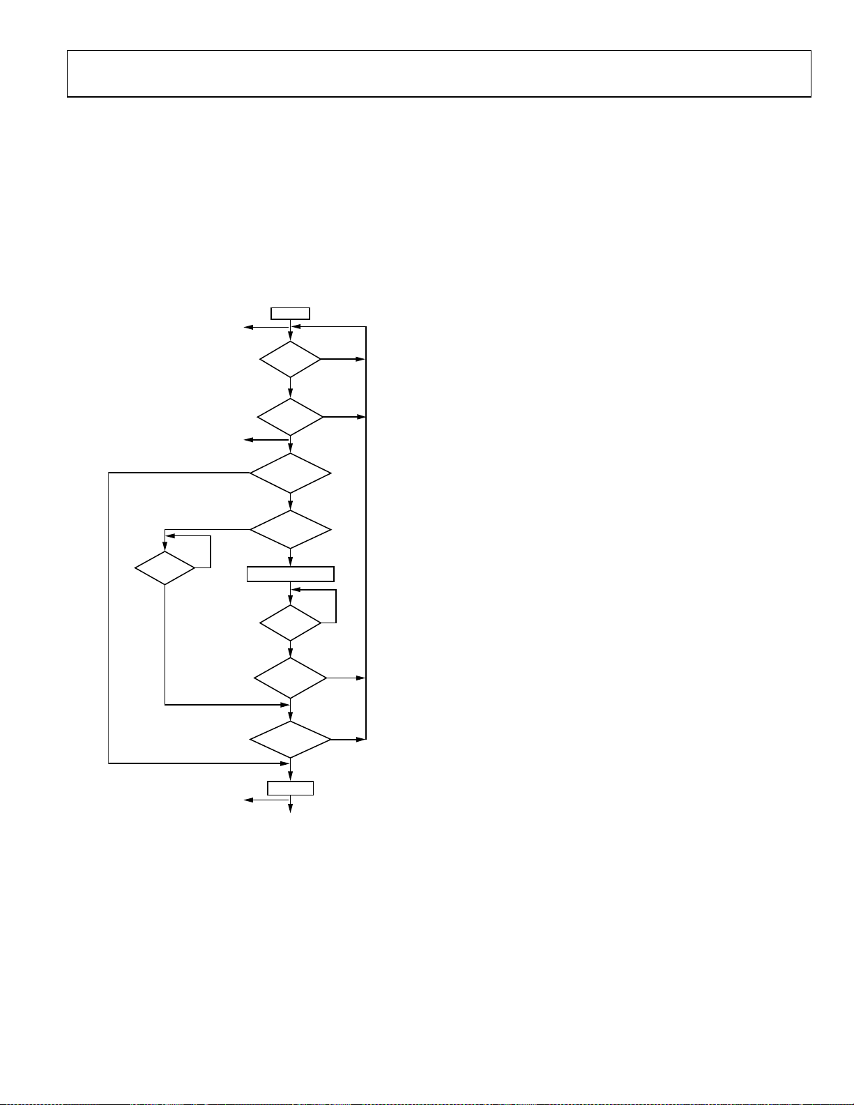
unlock process. Figure 15 shows a simple state diagram of the
unlocking process.
NO
UNLOCK EVENT
LOCKED
EVENT
DETECTED?
YES
FIRST
UNLOCK
EVENT?
YES
SECOND
REQUIR ED?
YES
NO
NO
LOCK_STAT = 1
LOCK_STAT = 1
When lock mode is enabled, no EVENT_INT interrupts can be
generated until the unlock events occur.
The ADP5589 features an interrupt mask timer, INT_MASK_
TIMER[4:0] (0x36[7:3]). When this timer and lock mode are
enabled, a single EVENT_INT is generated if any key is pressed
or any GPI (programmed to update the FIFO) is active. When
the EVENT_INT is generated, the mask timer begins counting.
No additional EVENT_INT interrupts are generated until
the mask timer expires and a new key is pressed or any GPI
(programmed to update the FIFO) is active, unless the unlock
events occur, in which case, normal operation is resumed.
Allowing a single EVENT_INT interrupt is useful to alert the
processor to turn on its screen and display an unlock message
to the user. Blanking out additional key presses ensures that the
processor is not unnecessarily interrupted until the unlock
events occur. Figure 16 shows the unlock sequence when the
interrupt mask timer is enabled.
UNLOCK
NO
TIMER
ENABLED?
EVENT
DETECTED?
YES
NO
LOCK_STAT = 0
START UNLOCK TIMER
YES
EVENT
DETECTED?
YES
UNLOCK
TIMER
EXPIRED?
NO
SECOND
UNLOCK EVEN T?
YES
UNLOCK
NO
YES
NO
09714-014
Figure 15. State Diagram of Unlocking Process
Rev. A | Page 13 of 48
Page 14
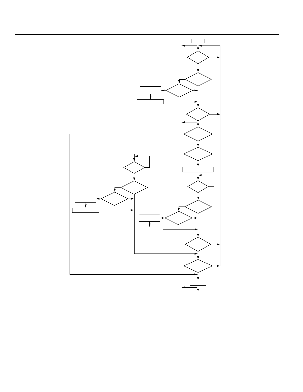
ADP5589
LOCKED
EVENT
DETECTED?
YES
MASK
TIMER ENABLED?
NO
NO
FIRST
UNLOCK
EVENT?
YES
SECOND
NO
UNLOCK EVENT
REQUIRED ?
YES
UNLOCK
NO
TIMER
ENABLED?
YES
START UNLOCK TIMER
NO
NO
EVENT
DETECTED?
YES
SET
EVENT_INT = 1
START MASK TIMER
NO
LOCK_STAT = 1
YES
YES
MASK
TIMER EXPI RED?
LOCK_STAT = 1
SET
EVENT_INT = 1
START MASK TIMER
YES
YES NO
TIMER EX PIRED?
TIMER E NABLED?
MASK
Figure 16. Unlock Sequence
MASK
NO
EVENT_INT = 1
START MASK TIM ER
YES NO
SET
LOCK_STAT = 0
YES
MASK
TIMER E XPIRED?
EVENT
DETECTED?
YES
MASK
TIMER ENABLED?
NO
UNLOCK
TIMER
EXPIRED?
NO
SECOND
UNLOCK EVENT ?
YES
UNLOCK
NO
YES
NO
09714-015
Rev. A | Page 14 of 48
Page 15

ADP5589
G
GPI Input
Each of the 19 I/O lines can be configured as a general-purpose
logic input line. Figure 17 shows a detailed representation of the
GPI scan and detect block and all its associated control and
status signals.
PIN_CONFIG _A[7:0]
PIN_CONFIG _B[7:0]
PIN_CONFIG _C[2:0]
EXT_LOCK_EVENT[7:0]
INT_MASK_TIMER[4:0]
GPIO_DIRECTION_A[7:0]
GPIO_DIRECTION_B[7:0]
GPIO_DIRECTION_C[2:0]
GPI_INT_LEVEL_A[7:0]
GPI_INT_LEVEL_B[7:0]
GPI_INT_LEVEL_C[2:0]
GPI_I NTERRUPT_EN_A[7:0]
GPI_I NTERRUPT_EN_B[7:0]
GPI_I NTERRUPT_EN_C[2:0]
GPI_EVENT_EN_A[ 7:0]
GPI_EVENT_EN_B[ 7:0]
GPI_EVENT_EN_C[ 2:0]
RESET_TRIGGER_TIME[2:0]
RESET1_EVENT_A[7: 0]
RESET1_EVENT_B[7: 0]
RESET1_EVENT_C[7: 0]
RESET2_EVENT_A[7: 0]
RESET2_EVENT_B[7: 0]
LOCK_EN
UNLOCK1[7:0]
UNLOCK2[7:0]
UNLOCK_T IMER[2:0 ]
LCK_TRK_GPI
GPIO 1
(R0)
GPIO 2
(R1)
GPIO 3
(R2)
GPIO 4
(R3)
GPIO 5
(R4)
GPIO 6
(R5)
GPIO 7
(R6)
GPIO 8
(R7)
GPIO 9
(C0)
GPIO 10
(C1)
GPIO 11
(C2)
GPIO 12
(C3)
GPIO 13
(C4)
GPIO 14
(C5)
GPIO 15
(C6)
GPIO 16
(C7)
GPIO 17
(C8)
GPIO 18
(C9)
GPIO 19
(C10)
GPI SCAN
CONTROL
LOCK_STAT
LOCK_INT
EVENT_INT
GPI_INT
GPI_INT_STAT_A[7:0]
GPI_INT_STAT_B[7:0]
GPI_INT_STAT_C[2:0]
GPI_ STATUS_A[7:0 ]
GPI_ STATUS_B[7:0 ]
GPI_ STATUS_C[2:0 ]
2
I
C BUSY?
KEY EVENT
GPI EVENT
LOGI C EVENT
FIFO
UPDATE
OVRFLOW_INT
EC[4:0]
FIFO
Figure 17. GPI Scan and Detect Block
The current input state of each GPI can be read back using the
GPI_STATUS_x registers. Each GPI can be programmed to
generate an interrupt via the GPI_INTERRUPT_EN_x registers.
The interrupt status is stored in the GPI_INT_STAT_x registers.
GPI interrupts can be programmed to trigger on inputs being
high or on inputs being low via the GPI_INT_LEVEL_x
registers. If any of the GPI interrupts is triggered, the master
GPI_INT interrupt is also triggered.
Figure 18 demonstrates a single GPI and how it affects its
corresponding status and interrupt status bits.
GPI 6
GPI_INT_LEVEL_A[5]
PI_INTERRUPT_ EN_A[5]
GPI_STATUS_A[ 5]
GPI_INT_STAT_A[5]
GPI_INT
CLEARED
BY READ
CLEARED
BY WRITE ‘1’
09714-017
Figure 18. Single GPI Example
GPIs can be programmed to generate FIFO events via the
GPI_EVENT_EN_x registers. GPIs in this mode do not generate GPI_INT interrupts and instead generate EVENT_INT
interrupts. Figure 19 shows several GPI lines and their effects
on the FIFO and event count, EC[4:0].
GPI 6
GPI 14
GPI 2
GPI SCAN
EVENT_INT
EC[4:0]
GPI 2 ACTIVE
GPI 6 ACTIVE
GPI 14 ACTIVE
GPI 14 INACT IVE
GPI 6 ACTIVE
GPI 2 ACTIVE
16
FIFO
1
101
105
1
113
1
113
0
105
0
101
0
234 5
09714-018
Figure 19. Multiple GPI Lines Example
The GPI scanner is idle until it detects a level transition. It scans
the GPI inputs and updates accordingly. It then returns to idle
immediately; it does not scan/wait, like the key scanner. As
such, the GPI scanner can detect narrow pulses once they get
past the 50 s input debounce filter.
09714-016
GPIs (programmed for FIFO updating) can be used as keypad
unlock events via the UNLOCKx registers (see the FIFO
Lock/Unlock section). The LCK_TRK_GPI bit can be used to
allow GPIs (programmed for FIFO updating) to be tracked
when the keypad is locked.
GPO OUTPUT
Each of the 19 I/O lines can be configured as a general-purpose
output (GPO) line. Figure 6 shows a detailed diagram of the I/O
structure. See the Detailed Register Descriptions section for
GPO configuration and usage.
Rev. A | Page 15 of 48
Page 16

ADP5589
LOGIC BLOCKS
Several of the ADP5589 I/O lines can be used as inputs and
outputs for implementing some common logic functions.
The R1, R2, and R3 I/O pins can be used as inputs, and the R0
I/O pin can be used as an output for Logic Block 1.
The C8, C7, and C6 I/O pins can be used as inputs, and the C9
I/O pin can be used as an output, for Logic Block 2. It is also
possible to cascade the output of Logic Block 1 as an alternate
input for Logic Block 2 (LY1 is used instead of LA2).
LOGIC BLOCK1
(R1) LA1
(R2)
LB1
(R3)
LC1
LA1_INV
LB1_INV
LC1_INV
LY1_INV
FF1_SET
FF1_CLR
LOGIC1_SEL[2:0]
R3_EXTEND_CFG[1:0]
LOGIC1_INT_LEVEL
LOGIC2_INT_LEVEL
LOGIC1_EVENT_EN
LOGIC2_EVENT_EN
RESET_TRIGGER_TI ME[2:0]
RESET1_EVENT_A[7:0]
RESET1_EVENT_B[7:0]
RESET1_EVENT_C[7:0]
RESET2_EVENT_A[7:0]
RESET2_EVENT_B[7:0]
LA1
0
IN_LA1
LB1
LB1
LC1
LC1
LA1
OUT
1
SEL
LA1_INV
0
OUT
1
SEL
LB1_INV
0
OUT
1
SEL
LC1_INV
IN_LB1
IN_LC1
LA1
LB1
LC1
R3_EXTEND_CFG[1:0] = 01
SET
D
Q
CLR
LCK_TRK_LOGIC
Figure 20. Logic Blocks Overview
IN_LA1
AND
IN_LB1
IN_LC1
IN_LA1
OR
IN_LB1
IN_LC1
IN_LA1
XOR
IN_LB1
IN_LC1
FF1_SET
IN_LA1
IN_LB1
FF1_CLR
IN_LC1
0
1
Figure 21. Logic Block 1
LY1 (R0)
LOGIC2_SEL[2:0]
C6_EXTEND_CFG
LOGIC
EVENT/INT
GENERATOR
AND
OR
XOR
OUT
SEL
The outputs from the logic blocks can be configured to generate
interrupts. They can also be configured to generate events on
the FIFO. The LCK_TRK_LOGIC (0x4D[4]) bit can be used
to allow logic events (programmed for FIFO updating) to be
tracked when the keypad is locked.
Figure 21 and Figure 22 show detailed diagrams of the internal
make-up of each logic block, illustrating the possible logic
functions that can be implemented.
LOGIC BLO CK2
(C8) LA2
(C7)
LB2
LC2
(C6)
LA2_INV
LB2_INV
0
OUT
1
SEL
0
OUT
1
SEL
0
OUT
1
SEL
SET
D
CLR
LC2_INV
LY2_INV
FF2_SET
FF2_CLR
2
I
C BUSY?
KEY EVENT
GPI EVENT
LOGIC EV ENT
AND1
OR1
XOR1
Q
FF1
SET
D
CLR
EVENT_INT
LOGIC1_INT
LOGIC2_INT
GND
AND1
OR1
XOR1
FF1
IN_LA1
IN_LB1
IN_LC1
LY2 (C9)
Q
OVRFLOW_INT
FIFO
UPDATE
MUX
000
001
010
011
OUT
100
101
110
111
SEL[2:0]
LOGIC1_SEL[2:0]
EC[4:0]
FIFO
LY1
LY1
09714-019
0
OUT
1
SEL
LY1_INV
LY1
09714-020
Rev. A | Page 16 of 48
Page 17

ADP5589
LA2
0
1
LY1
LY1_CASCADE
OUT
SEL
LB2
LC2
C6_EXTEND_CFG = 1
(LY1)
LA2
LA2
(LY1)
LB2
LB2
LC2
LC2
0
OUT
1
SEL
LA2_INV
0
OUT
1
SEL
LB2_INV
0
OUT
1
SEL
LC2_INV
(IN_LY1)
IN_LA2
IN_LB2
IN_LC2
(IN_LY1)
IN_LA2
IN_LB2
IN_LC2
(IN_LY1)
IN_LA2
IN_LB2
IN_LC2
(IN_LY1)
IN_LA2
IN_LB2
IN_LC2
IN_LA2
IN_LB2
FF2_CLR
IN_LC2
AND
OR
XOR
FF2_SET
0
AND2
OUT
1
AND
SEL
0
OR2
OUT
1
OR
SEL
0
OUT
1
XOR
SEL
SET
D
0
1
CLR
OUT
SEL
IN_LA2
XOR2
IN_LB2
IN_LC2
Q
FF2
GND
AND2
OR2
XOR2
FF2
MUX
000
001
010
011
OUT
100
101
110
111
SEL[2:0]
LOGIC2_SEL
LY2
LY2
0
OUT
1
SEL
LY2_INV
LY2
9714-021
Figure 22. Logic Block 2
PWM_EN
PWM_MODE
PWM_OFFT_LOW_BYTE[7:0]
PWM_OF FT_HIG H_BYTE[7: 0]
PWM_ONT_LOW_BYTE[7:0]
PWM_ONT_HIGH_BYTE[7:0]
(C6) PWM_IN
PWM_IN_AND
OFF TIME[15:0]
ON TIME[15:0]
PWM
GENERATO R
Figure 23. PWM Block Diagram
0
1
AND
OUT
SEL
(R3)
PWM_OUT
09714-022
PWM BLOCK
The ADP5589 features a PWM generator whose output can be
configured to drive out on I/O Pin R3. PWM on/off times are
programmed via four 8-bit registers.
Newly programmed values are not latched until the final byte,
PWM_ONT_HIGH_BYTE (Address 0x41, Bits[7:0]), is written
to (see Figure 23).
The highest frequency obtainable from the PWM is performed
by setting the least significant bit (LSB) of both the on and off
bit patterns, resulting in a 500 kHz signal with a 50% duty cycle.
Each LSB respresents 1 µs of on or off time.
The PWM block provides support for continuous PWM
mode as well as a one-shot mode (see Tab l e 7 4 ). Additionally,
an external signal can be AND’ed with the internal PWM signal.
This option can be selected by writing a 1 to PWM_IN_AND,
PWM_CFG[2]. The input to the external AND is the C6 I/O
pin. C6 should be set to GPI (GPIO15). Note that the debounce
for C6 will result in a delay of the AND’ing, and can be
controlled using register GPI_15_DEB_DIS (Address 0x28,
Bit[6]).
Newly programmed values are not latched until the final byte,
PWM_ONT_HIGH_BYTE (Address 0x41, Bits[7:0]), is written.
CLOCK DIVIDER BLOCK
The ADP5589 features a clock divider block that divides down
the frequency of an externally supplied source via I/O Pin C6.
The output of the divider is driven out on I/O Pin R3.
CLK_DIV_EN
CLK_DIV[4:0]
CLK_IN
(C6)
CLK_INV
CLK
DIVIDER
0
1
OUT
SEL
Figure 24. Clock Divider Block
(R3)CLK_OUT
09714-023
RESET BLOCKS
The ADP5589 features two reset blocks that can generate reset
conditions if certain events are detected at the same time. Up to
three reset trigger events can be programmed for RESET1. Up
to two reset trigger events can be programmed for RESET2. The
event scan control blocks monitor whether these events are present
for the duration of RESET_TRIGGER_TIME[2:0] (0x3D[4:2]).
If they are, reset-initiate signals are sent to the reset generator
blocks. The generated reset signal pulse width is programmable.
Rev. A | Page 17 of 48
Page 18

ADP5589
RST
RESET1_
INITIATE
RESET_PULSE_WIDTH[1:0]
RESET2_
INITIATE
RESET
GEN 1
RESET
GEN 2
RESET1
RESET2
(R4)
(C4)
RESET_TRIGGER_TIME[2:0]
RESET1_EVENT _A[7:0]
RESET1_EVENT _B[7:0]
RESET1_EVENT _C[7:0]
RESET2_EVENT _A[7:0]
RESET2_EVENT _B[7:0]
RST_PASSTHRU_EN
KEY
SCAN
CONTROL
GPI
SCAN
CONTROL
LOGIC
BLOCK
CONTROL
Figure 25. Reset Blocks
The RESET1 signal uses I/O Pin R4 as its output. A passthrough mode allows the main
RST
pin to be output on the
R4 pin also.
The RESET2 signal uses I/O Pin C4 as its output.
The reset generation signals are useful in situations where the
system processor has locked up and the system is unresponsive
to input events. The user can press one of the reset event combinations and initiate a system-wide reset. This alleviates the need
for removing the battery from the system and performing a
hard reset.
It is not recommended to use the immediate trigger time (see
the details of the RESET_CFG Register, 0x3D, in Tab l e 69 )
because this setting may cause false triggering.
INTERRUPTS
INT
The
sources is active. The user can select which internal interrupts
interact with the external interrupt pin in register INT_EN
(Address 0x4E, Bits[7:0]) (refer to ). allows the user to
choose whether the external interrupt pin remains asserted, or
deasserts for 50 µs, then reasserts, in the case that there are
multiple internal interrupts asserted, and one is cleared (refer
to ).
9714-024
pin can be asserted low if any of the internal interrupt
Tabl e 86
Tabl e 85
EVENT_INT
EVENT_IEN
GPI_INT
GPI_IEN
LOGIC1_INT
LOGIC1_IEN
LOGI C2_INT
LOGIC2_IEN
OVRFLOW_INT
OVRFLOW_IEN
LOCK_INT
LOCK_IEN
Figure 26. Asserting
INT DRIVE
INT_CFG
INT
INT
09714-025
Low
Rev. A | Page 18 of 48
Page 19

ADP5589
E
E
REGISTER INTERFACE
Register access of the ADP5589 is acquired via its I2C-compatible
serial interface. The interface can support clock frequencies of
up to 1 MHz. If the user is accessing the FIFO or key event
counter (KEC), FIFO/KEC updates are paused. If the clock
frequency is very low, events may not be recorded in a timely
manner. FIFO or KEC updates can happen up to 23 µs after an
interrupt is asserted because of the number of I
to perform an I
2
C read or write. This delay should not present
2
C cycles required
an issue to the user.
Figure 27 shows a typical write sequence for programming an
internal register. The cycle begins with a start condition, followed
by the hard coded 7-bit device address, which for the ADP5589
is 0x34, followed by the R/
ADP5589
acknowledges the address byte by pulling the data line
W
bit set to 0 for a write cycle. The
low. The address of the register to which data is to be written is
sent next. The acknowledges the register pointer byte
ADP5589
by pulling the data line low. The data byte to be written is sent
next. The acknowledges the data byte by pulling the
ADP5589
data line low. A stop condition completes the sequence.
Figure 28 shows a typical multibyte write sequence for programming internal registers. The cycle begins with a start condition
followed by the 7-bit device address (0x34), followed by the
START
0 = WRIT
W
R/
bit set to 0 for a write cycle. The acknowledges
ADP5589
the address byte by pulling the data line low. The address of the
register to which data is to be written is sent next. The
ADP5589
acknowledges the register pointer byte by pulling the data line
low. The data byte to be written is sent next. The
ADP5589
acknowledges the data byte by pulling the data line low. The
pointer address is then incremented to write the next data byte,
until it finishes writing the n data byte. The pulls the
ADP5589
data line low after every byte, and a stop condition completes
the sequence.
Figure 29 shows a typical byte read sequence for reading internal
registers. The cycle begins with a start condition followed by the
7-bit device address (0x34), followed by the R/
a write cycle. The acknowledges the address byte by
ADP5589
W
bit set to 0 for
pulling the data line low. The address of the register from which
data is to be read is sent next. The acknowledges the
ADP5589
register pointer byte by pulling the data line low. A start condition is repeated, followed by the 7-bit device address (0x34),
followed by the R/
W
bit set to 1 for a read cycle. The
ADP5589
acknowledges the address byte by pulling the data line low. The
8-bit data is then read. The host pulls the data line high (no
acknowledge), and a stop condition completes the sequence.
STOP
7-BIT DEVICE ADDRESS
ADP5589 ACK
8-BIT REG ISTER POINTER 8-BI T WRITE DATA00 0 0
ADP5589 ACK
Figure 27. I
2
C Single-Byte Write Sequence
ADP5589 ACK
09714-026
START
7-BIT DEVICE ADDRESS
0 = WRIT
ADP5589 ACK
8-BIT REGISTER POINTER WRITE BYTE 1 WRITE BYTE 2 WRITE BYTE n00 0 0 0 0 0
ADP5589 ACK ADP5589 ACK ADP5589 ACK ADP5589 ACK
Figure 28. I
2
C Multibyte Write Sequence
STOP
ADP5589 ACK
09714-028
START
7-BIT DEVICE ADDRESS 7-BIT DEVICE ADDRESS
0 = WRITE
8-BIT REGISTER POI NTER 8-BIT READ DATA00 0 1 0 1
ADP5589 ACK
Figure 29. I
REPEAT START 1 = READ
ADP5589 ACK ADP5589 ACK
2
C Single-Byte Read Sequence
STOP
NO ACK
09714-027
Rev. A | Page 19 of 48
Page 20

ADP5589
Figure 30 shows a typical multibyte read sequence for reading
internal registers. The cycle begins with a start condition, followed
by the 7-bit device address (0x34), followed by the R/
to 0 for a write cycle. The acknowledges the address
ADP5589
byte by pulling the data line low. The address of the register
from which data is to be read is sent next. The acknowl-
ADP5589
edges the register pointer byte by pulling the data line low. A start
condition is repeated, followed by the 7-bit device address (0x34),
START
0 = WRITE
W
bit set
REPEAT START 1 = READ
followed by the R/
W
bit set to 1 for a read cycle. The
ADP5589
acknowledges the address byte by pulling the data line low. The
8-bit data is then read. The address pointer is then incremented
to read the next data byte, and the host continues to pull the data
line low for each byte (master acknowledge) until the n data
byte is read. The host pulls the data line high (no acknowledge)
after the last byte is read, and a stop condition completes the
sequence.
STOP
7-BIT DEVI CE ADDRESS 7- BIT DEVICE ADDRESS
8-BIT REG ISTER POI NTER READ BYTE 1 READ BYTE 2 READ BYTE n00 0 10 0 0 0 1
ADP5589 ACK
ADP5589 ACK ADP5589 ACK MASTER ACK MASTER ACK MASTER ACK
Figure 30. I
2
C Multibyte Read Sequence
NO ACK
09714-029
Rev. A | Page 20 of 48
Page 21

ADP5589
REGISTER MAP
Table 6.
Addr. R/W Bit 7 Bit 6 Bit 5 Bit 4 Bit 3 Bit 2 Bit 1 Bit 0
0x00 R MAN_ID REV_ID
0x01 R/W Reserved LOGIC2_INT LOGIC1_
INT
0x02 R LOGIC2_STAT LOGIC1_STAT LOCK_STAT EC[4:0]
0x03 R Event1_State EVENT1_IDENTIFIER[6:0]
0x04 R Event2_State EVENT2_IDENTIFIER[6:0]
0x05 R Event3_State EVENT3_IDENTIFIER[6:0]
0x06 R Event4_State EVENT4_IDENTIFIER[6:0]
0x07 R Event5_State EVENT5_IDENTIFIER[6:0]
0x08 R Event6_State EVENT6_IDENTIFIER[6:0]
0x09 R Event7_State EVENT7_IDENTIFIER[6:0]
0x0A R Event8_State EVENT8_IDENTIFIER[6:0]
0x0B R Event9_State EVENT9_IDENTIFIER[6:0]
0x0C R Event10_State EVENT10_IDENTIFIER[6:0]
0x0D R Event11_State EVENT11_IDENTIFIER[6:0]
0x0E R Event12_State EVENT12_IDENTIFIER[6:0]
0x0F R Event13_State EVENT13_IDENTIFIER[6:0]
0x10 R Event14_State EVENT14_IDENTIFIER[6:0]
0x11 R Event15_State EVENT15_IDENTIFIER[6:0]
0x12 R Event16_State EVENT16_IDENTIFIER[6:0]
0x13 R GPI_INT_STAT_A[7:0]
0x14 R GPI_INT_STAT_B[7:0]
0x15 R Reserved GPI_INT_STAT_C[2:0]
0x16 R GPI_STATUS_A[7:0]
0x17 R GPI_STATUS_B[7:0]
0x18 R Reserved GPI_STATUS_C[2:0]
0x19 R/W RPULL_CONFIG_A[7:0]
0x1A R/W RPULL_CONFIG_B[7:0]
0x1B R/W RPULL_CONFIG_C[7:0]
0x1C R/W RPULL_CONFIG_D[7:0]
0x1D R/W Reserved RPULL_CONFIG_E[5:0]
0x1E R/W GPI_INT_LEVEL_A[7:0]
0x1F R/W GPI_INT_LEVEL_B[7:0]
0x20 R/W Reserved GPI_INT_LEVEL_C[2:0]
0x21 R/W GPI_EVENT_EN_A[7:0]
0x22 R/W GPI_EVENT_EN_B[7:0]
0x23 R/W Reserved GPI_EVENT_EN_C[2:0]
0x24 R/W GPI_INTERRUPT_EN_A[7:0]
0x25 R/W GPI_INTERRUPT_EN_B[7:0]
0x26 R/W Reserved GPI_INTERRUPT_EN_C[2:0]
0x27 R/W DEBOUNCE_DIS_A[7:0]
0x28 R/W DEBOUNCE_DIS_B[7:0]
0x29 R/W Reserved DEBOUNCE_DIS_C[2:0]
0x2A R/W GPO_DATA_OUT_A[7:0]
0x2B R/W GPO_DATA_OUT_B[7:0]
0x2C R/W Reserved GPO_DATA_OUT_C[2:0]
0x2D R/W GPO_OUT_MODE_A[7:0]
0x2E R/W GPO_OUT_MODE_B[7:0]
0x2F R/W Reserved GPO_OUT_MODE_C[2:0]
0x30 R/W GPIO_DIRECTION_A[7:0]
0x31 R/W GPIO_DIRECTION_B[7:0]
0x32 R/W Reserved GPIO_DIRECTION_C[2:0]
LOCK_INT OVRFLOW_
INT
GPI_INT EVENT_INT
Rev. A | Page 21 of 48
Page 22

ADP5589
Addr. R/W Bit 7 Bit 6 Bit 5 Bit 4 Bit 3 Bit 2 Bit 1 Bit 0
0x33 R/W UNLOCK1_
0x34 R/W UNLOCK2_
0x35 R/W EXT_LOCK_
0x36 R/W INT_MASK_TIMER[4:0] UNLOCK_TIMER[2:0]
0x37 R/W Reserved LOCK_EN
0x38 R/W RESET1_
0x39 R/W RESET2_
0x3A R/W RESET1_
0x3B R/W RESET1_
0x3C R/W RESET1_
0x3D R/W RESET2_POL RESET1_POL
0x3E R/W PWM_OFFT_LOW_BYTE[7:0]
0x3F R/W PWM_OFFT_HIGH_BYTE[7:0]
0x40 R/W PWM_ONT_LOW_BYTE[7:0]
0x41 R/W PWM_ONT_HIGH_BYTE[7:0]
0x42 R/W Reserved PWM_IN_AND PWM_MODE PWM_EN
0x43 R/W Reserved CLK_INV CLK_DIV[4:0] CLK_DIV_EN
0x44 R/W Reserved LY1_INV LC1_INV LB1_INV LA1_INV LOGIC1_SEL[2:0]
0x45 R/W LY1_CASCADE LY2_INV LC2_INV LB2_INV LA2_INV LOGIC2_SEL[2:0]
0x46 R/W Reserved FF2_SET FF2_CLR FF1_SET FF1_CLR
0x47 R/W Reserved LY2_DBNC_DIS LOGIC2_
0x48 R/W Reserved KEY_POLL_TIME[1:0]
0x49 R/W PIN_CONFIG_A[7:0]
0x4A R/W PIN_CONFIG_B[7:0]
0x4B R/W Reserved PIN_CONFIG_C[2:0]
0x4C R/W PULL_SELECT C4_EXTEND_
0x4D R/W OSC_EN CORE_FREQ[1:0] LCK_TRK_
0x4E R/W Reserved LOGIC2_IEN LOGIC1_
STATE
STATE
STATE
EVENT_A Level
EVENT_B Level
EVENT_B Level
EVENT_B Level
EVENT_B Level
CFG
RST_
PASSTHRU_EN
R4_EXTEND_
CFG
EVENT_EN
C6_
EXTEND_CFG
LOGIC
IEN
UNLOCK1[6:0]
UNLOCK2[6:0]
EXT_LOCK_EVENT[6:0]
RESET1_EVENT_A[6:0]
RESET1_EVENT_B[6:0]
RESET1_EVENT_C[6:0]
RESET2_EVENT_A[6:0]
RESET2_EVENT_B[6:0]
RESET_TRIGGER_TIME[2:0] RESET_PULSE_WIDTH[1:0]
LOGIC2_INT_
LEVEL
R3_EXTEND_CFG[1:0] C9_EXTEND_
LCK_TRK_GPI
LOCK_IEN OVRFLOW_
LY1_DBNC_
DIS
IEN
LOGIC1_
EVENT_EN
CFG
LOGIC1_INT_
LEVEL
R0_EXTEND_
CFG
INT_CFG RST_CFG
GPI_IEN EVENT_IEN
Rev. A | Page 22 of 48
Page 23

ADP5589
DETAILED REGISTER DESCRIPTIONS
ID Register 0x00
Table 7. ID Bit Descriptions
Bits Name R/W Description
[7: 4] MAN_ID R Manufacturer ID, default = 0001.
[3:0] REV_ID R Rev ID.
INT_STATUS Register 0x01
Table 8. INT_STATUS Bit Descriptions
Bits Name R/W Description
[7: 6] N/A Reserved.
5 LOGIC2_INT R/W 0 = no interrupt.
1 = interrupt due to a general Logic 2 condition.
Write a 1 to this bit to clear it.
4 LOGIC1_INT R/W 0 = no interrupt.
1 = interrupt due to a general Logic 1 condition.
Write a 1 to this bit to clear it.
3 LOCK_INT R/W 0 = no interrupt.
1 = interrupt due to a lock/unlock condition.
The user can read LOCK_STAT (0x02[5]) to determine if LOCK_INT is due to a lock or unlock event.
If LOCK_STAT = 1, LOCK_INT is due to a lock event.
If LOCK_STAT = 0, LOCK_INT is due to an unlock event.
Write a 1 to this bit to clear it.
If lock mode is enabled via the software bit LOCK_EN (0x37[0]), a LOCK_INT is not generated
because the processor knows it just enabled lock mode.
If lock mode is disabled (while locked) via the software bit LOCK_EN, a LOCK_INT is not generated
because the processor knows it just disabled lock mode.
2 OVRFLOW_INT R/W 0 = no interrupt.
1 = interrupt due to an overflow condition.
Write a 1 to this bit to clear it.
1 GPI_INT R/W 0 = no interrupt.
1 = interrupt due to a general GPI condition.
This bit is not set by a GPI that has been configured to update the FIFO and event count.
Write a 1 to this bit to clear it.
This bit cannot be cleared until all GPI_x_INT bits are cleared.
0 EVENT_INT R/W 0 = no interrupt.
1 = interrupt due to key event (press/release), GPI event (GPI programmed for FIFO updates), or
Logic 1/Logic 2 event (programmed for FIFO updates).Write a 1 to this bit to clear it.
Status Register 0x02
Table 9. Status Bit Descriptions
Bits Name R/W Description
7 LOGIC2_STAT R 0 = output from Logic Block 2. (LY2) is low.
1 = output from
6 LOGIC1_STAT R 0 = output from Logic Block 1 (LY1) is low.
1 = output from Logic Block 1 (LY1) is high.
5 LOCK_STAT R 0 = unlocked.
1 = locked.
[4:0] EC[4:0] R Event count value. Indicates how many events are currently stored on the FIFO.
Logic Block 2. (LY2) is high.
Rev. A | Page 23 of 48
Page 24

ADP5589
FIFO_1 Register 0x03
Table 10. FIFO_1 Bit Descriptions
Bits Name R/W Description
7 Event1_State R
[6:0] EVENT1_IDENTIFIER[6:0] This bit represents the state of the event that is recorded in EVENT1_IDENTIFIER[6:0].
Table 11. Event Decoding
Event No. Meaning Event No. Meaning Event No. Meaning Event No. Meaning
0 No event 32 Key 32 (R2, C9) 64 Key 64 (R5, C8) 96 Key 96 (R7, GND)
1 Key 1 (R0, C0) 33 Key 33 (R2, C10) 65 Key 65 (R5, C9) 97 GPI 1 (R0)
2 Key 2 (R0, C1) 34 Key 34 (R3, C0) 66 Key 66 (R5, C10) 98 GPI 2 (R1)
3 Key 3 (R0, C2) 35 Key 35 (R3, C1) 67 Key 67 (R6, C0) 99 GPI 3 (R2)
4 Key 4 (R0, C3) 36 Key 36 (R3, C2) 68 Key 68 (R6, C1) 100 GPI 4 (R3)
5 Key 5 (R0, C4) 37 Key 37 (R3, C3) 69 Key 69 (R6, C2) 101 GPI 5 (R4)
6 Key 6 (R0, C5) 38 Key 38 (R3, C4) 70 Key 70 (R6, C3) 102 GPI 6 (R5)
7 Key 7 (R0, C6) 39 Key 39 (R3, C5) 71 Key 71 (R6, C4) 103 GPI 7 (R6)
8 Key 8 (R0, C7) 40 Key 40 (R3, C6) 72 Key 72 (R6, C5) 104 GPI 8 (R7)
9 Key 9 (R0, C8) 41 Key 41 (R3, C7) 73 Key 73 (R6, C6) 105 GPI 9 (C0)
10 Key 10 (R0, C9) 42 Key 42 (R3, C8) 74 Key 74 (R6, C7) 106 GPI 10 (C1)
11 Key 11 (R0, C10) 43 Key 43 (R3, C9) 75 Key 75 (R6, C8) 107 GPI 11 (C2)
12 Key 12 (R1, C0) 44 Key 44 (R3, C10) 76 Key 76 (R6, C9) 108 GPI 12 (C3)
13 Key 13 (R1, C1) 45 Key 45 (R4, C0) 77 Key 77 (R6, C10) 109 GPI 13 (C4)
14 Key 14 (R1, C2) 46 Key 46 (R4, C1) 78 Key 78 (R7, C0) 110 GPI 14 (C5)
15 Key 15 (R1, C3) 47 Key 47 (R4, C2) 79 Key 79 (R7, C1) 111 GPI 15 (C6)
16 Key 16 (R1, C4) 48 Key 48 (R4, C3) 80 Key 80 (R7, C2) 112 GPI 16 (C7)
17 Key 17 (R1, C5) 49 Key 49 (R4, C4) 81 Key 81 (R7, C3) 113 GPI 17 (C8)
18 Key 18 (R1, C6) 50 Key 50 (R4, C5) 82 Key 82 (R7, C4) 114 GPI 18 (C9)
19 Key 19 (R1, C7) 51 Key 51 (R4, C6) 83 Key 83 (R7, C5) 115 GPI 19 (C10)
20 Key 20 (R1, C8) 52 Key 52 (R4, C7) 84 Key 84 (R7, C6) 116 Logic 1
21 Key 21 (R1, C9) 53 Key 53 (R4, C8) 85 Key 85 (R7, C7) 117 Logic 2
22 Key 22 (R1, C10) 54 Key 54 (R4, C9) 86 Key 86 (R7, C8) 118 Unused
23 Key 23 (R2, C0) 55 Key 55 (R4, C10) 87 Key 87 (R7, C9) 119 Unused
24 Key 24 (R2, C1) 56 Key 56 (R5, C0) 88 Key 88 (R7, C10) 120 Unused
25 Key 25 (R2, C2) 57 Key 57 (R5, C1) 89 Key 89 (R0, GND) 121 Unused
26 Key 26 (R2, C3) 58 Key 58 (R5, C2) 90 Key 90 (R1, GND) 122 Unused
27 Key 27 (R2, C4) 59 Key 59 (R5, C3) 91 Key 91 (R2, GND) 123 Unused
28 Key 28 (R2, C5) 60 Key 60 (R5, C4) 92 Key 92 (R3, GND) 124 Unused
29 Key 29 (R2, C6) 61 Key 61 (R5, C5) 93 Key 93 (R4, GND) 125 Unused
30 Key 30 (R2, C7) 62 Key 62 (R5, C6) 94 Key 94 (R5, GND) 126 Unused
31 Key 31 (R2, C8) 63 Key 63 (R5, C7) 95 Key 95 (R6, GND) 127 Wildcard for unlock
The seven lower bits of each FIFO location contain the event identifier, which can be
decoded to reveal the event recorded.
Table 11 outlines each event number, what it represents, and the I/O pins associated with it.
Bit 7 is the Event 1 state.
For key events (Event 1 to Event 96).
1 = key is pressed.
0 = key is released.
For GPI and logic events (Event 97 to Event 117).
1 = GPI/logic is active.
0 = GPI/logic is inactive.
Active and inactive states are programmable.
Rev. A | Page 24 of 48
Page 25

ADP5589
FIFO_2 Register 0x04
Table 12. FIFO_2 Bit Descriptions
Bits Name R/W Description
7 Event2_State R Refer to Table 10.
[6:0] EVENT2_IDENTIFIER[6:0] R Refer to Table 10.
FIFO_3 Register 0x05
Table 13. FIFO_3 Bit Descriptions
Bits Name R/W Description
7 Event3_State R Refer to Table 10.
[6: 0] EVENT3_IDENTIFIER[6:0] R Refer to Table 10.
FIFO_4 Register 0x06
Table 14. FIFO_4 Bit Descriptions
Bits Name R/W Description
7 Event4_State R Refer to Table 10.
[6:0] EVENT4_IDENTIFIER[6:0] R Refer to Table 1 0.
FIFO_5 Register 0x07
Table 15. FIFO_5 Bit Descriptions
Bits Name R/W Description
7 Event5_State R Refer to Table 10.
[6:0] EVENT5_IDENTIFIER[6:0] R Refer to Table 1 0.
FIFO_6 Register 0x08
Table 16. FIFO_6 Bit Descriptions
Bits Name R/W Description
7 Event6_State R Refer to Table 10.
[6:0] EVENT6_IDENTIFIER[6:0] R Refer to Table 1 0.
FIFO_7 Register 0x09
Table 17. FIFO_7 Bit Descriptions
Bits Name R/W Description
7 Event7_State R Refer to Table 10.
[6:0] EVENT7_IDENTIFIER[6:0] R Refer to Table 1 0.
FIFO_8 Register 0x0A
Table 18. FIFO_8 Bit Descriptions
Bits Name R/W Description
7 Event8_State R Refer to Table 10.
[6:0] EVENT8_IDENTIFIER[6:0] R Refer to Table 1 0.
FIFO_9 Register 0x0B
Table 19. FIFO_9 Bit Descriptions
Bits Name R/W Description
7 Event9_State R Refer to Table 10.
[6:0] EVENT9_IDENTIFIER[6:0] R Refer to Table 1 0.
Rev. A | Page 25 of 48
Page 26

ADP5589
FIFO_10 Register 0x0C
Table 20. FIFO_10 Bit Descriptions
Bits Name R/W Description
7 Event10_State R Refer to Table 10.
[6:0] EVENT10_IDENTIFIER[6:0] R Refer to Table 10.
FIFO_11 Register 0x0D
Table 21. FIFO_11 Bit Descriptions
Bits Name R/W Description
7 Event11_State R Refer to Table 10.
[6:0] EVENT11_IDENTIFIER[6:0] R Refer to Table 10.
FIFO_12 Register 0x0E
Table 22. FIFO_12 Bit Descriptions
Bits Name R/W Description
7 Event12_State R Refer to Table 10.
[6:0] EVENT12_IDENTIFIER[6:0] R Refer to Table 10.
FIFO_13 Register 0x0F
Table 23. FIFO_13 Bit Descriptions
Bits Name R/W Description
7 Event13_State R Refer to Table 10.
[6:0] EVENT13_IDENTIFIER[6:0] R Refer to Table 10.
FIFO_14 Register 0x10
Table 24. FIFO_14 Bit Descriptions
Bits Name R/W Description
7 Event14_State R Refer to Table 10.
[6: 0] EVENT14_IDENTIFIER[6:0] R Refer to Table 1 0.
FIFO_15 Register 0x11
Table 25. FIFO_15 Bit Descriptions
Bits Name R/W Description
7 Event15_State R Refer to Table 10.
[6: 0] EVENT15_IDENTIFIER[6:0] R Refer to Table 1 0.
FIFO_16 Register 0x12
Table 26. FIFO_16 Bit Descriptions
Bits Name R/W Description
7 Event16_State R Refer to Table 10.
[6: 0] EVENT16_IDENTIFIER[6:0] R Refer to Table 1 0.
Rev. A | Page 26 of 48
Page 27

ADP5589
GPI_INT_STAT_A Register 0x13
Table 27. GPI_INT_STAT_A Bit Descriptions
Bits Name R/W Description
7 GPI_8_INT R 0 = no interrupt.
1 = interrupt due to GPI_8 (R7 pin). Cleared on read.
6 GPI_7_INT R 0 = no interrupt.
1 = interrupt due to GPI_7 (R6 pin). Cleared on read.
5 GPI_6_INT R 0 = no interrupt.
1 = interrupt due to GPI_6 (R5 pin). Cleared on read.
4 GPI_5_INT R 0 = no interrupt.
1 = interrupt due to GPI_5 (R4 pin). Cleared on read.
3 GPI_4_INT R 0 = no interrupt.
1 = interrupt due to GPI_4 (R3 pin). Cleared on read.
2 GPI_3_INT R 0 = no interrupt.
1 = interrupt due to GPI_3 (R2 pin). Cleared on read.
1 GPI_2_INT R 0 = no interrupt.
1 = interrupt due to GPI_2 (R1 pin). Cleared on read.
0 GPI_1_INT R 0 = no interrupt.
1 = interrupt due to GPI_1 (R0 pin). Cleared on read.
GPI_INT_STAT_B Register 0x14
Table 28. GPI_INT_STAT_B Bit Descriptions
Bits Name R/W Description
7 GPI_16_INT R 0 = no interrupt.
1 = interrupt due to GPI_16 (C7 pin). Cleared on read.
6 GPI_15_INT R 0 = no interrupt.
1 = interrupt due to GPI_15 (C6 pin). Cleared on read.
5 GPI_14_INT R 0 = no interrupt.
1 = interrupt due to GPI_14 (C5 pin). Cleared on read.
4 GPI_13_INT R 0 = no interrupt.
1 = interrupt due to GPI_13 (C4 pin). Cleared on read.
3 GPI_12_INT R 0 = no interrupt.
1 = interrupt due to GPI_12 (C3 pin). Cleared on read.
2 GPI_11_INT R 0 = no interrupt.
1 = interrupt due to GPI_11 (C2 pin). Cleared on read.
1 GPI_10_INT R 0 = no interrupt.
1 = interrupt due to GPI_10 (C1 pin). Cleared on read.
0 GPI_9_INT R 0 = no interrupt.
1 = interrupt due to GPI_9 (C0 pin). Cleared on read.
GPI_INT_STAT_C Register 0x15
Table 29. GPI_INT_STAT_C Bit Descriptions
Bits Name R/W Description
[7: 3] Reserved.
2 GPI_19_INT R 0 = no interrupt.
1 = interrupt due to GPI_19 (C10 pin). Cleared on read.
1 GPI_18_INT R 0 = no interrupt.
1 = interrupt due to GPI_18 (C9 pin). Cleared on read.
0 GPI_17_INT R 0 = no interrupt.
1 = interrupt due to GPI_17 (C8 pin). Cleared on read.
Rev. A | Page 27 of 48
Page 28

ADP5589
GPI_STATUS_A Register 0x16
Table 30. GPI_STATUS_A Bit Descriptions
Bits Name R/W Description
7 GPI_8_STAT R 0 = GPI_8 (R7 pin) is low.
1 = GPI_8 (R7 pin) is high.
6 GPI_7_STAT R 0 = GPI_7 (R6 pin) is low.
1 = GPI_7 (R6 pin) is high.
5 GPI_6_STAT R 0 = GPI_6 (R5 pin) is low.
1 = GPI_6 (R5 pin) is high.
4 GPI_5_STAT R 0 = GPI_5 (R4 pin) is low.
1 = GPI_5 (R4 pin) is high.
3 GPI_4_STAT R 0 = GPI_4 (R3 pin) is low.
1 = GPI_4 (R3 pin) is high.
2 GPI_3_STAT R 0 = GPI_3 (R2 pin) is low.
1 = GPI_3 (R2 pin) is high.
1 GPI_2_STAT R 0 = GPI_2 (R1 pin) is low.
1 = GPI_2 (R1 pin) is high.
0 GPI_1_STAT R 0 = GPI_1 (R0 pin) is low.
1 = GPI_1 (R0 pin) is high.
GPI_STATUS_B Register 0x17
Table 31. GPI_STATUS_B Bit Descriptions
Bits Name R/W Description
7 GPI_16_STAT R 0 = GPI_16 (C7 pin) is low.
1 = GPI_16 (C7 pin) is high.
6 GPI_15_STAT R 0 = GPI_15 (C6 pin) is low.
1 = GPI_15 (C6 pin) is high.
5 GPI_14_STAT R 0 = GPI_14 (C5 pin) is low.
1 = GPI_14 (C5 pin) is high.
4 GPI_13_STAT R 0 = GPI_13 (C4 pin) is low.
1 = GPI_13 (C4 pin) is high.
3 GPI_12_STAT R 0 = GPI_12 (C3 pin) is low.
1 = GPI_12 (C3 pin) is high.
2 GPI_11_STAT R 0 = GPI_11 (C2 pin) is low.
1 = GPI_11 (C2 pin) is high.
1 GPI_10_STAT R 0 = GPI_10 (C1 pin) is low.
1 = GPI_10 (C1 pin) is high.
0 GPI_9_STAT R 0 = GPI_9 (C0 pin) is low.
1 = GPI_9 (C0 pin) is high.
GPI_STATUS_C Register 0x18
Table 32. GPI_STATUS_C Bit Descriptions
Bits Name R/W Description
[7: 3] Reserved.
2 GPI_19_STAT R 0 = GPI_19 (C10 pin) is low.
1 = GPI_19 (C10 pin) is high.
1 GPI_18_STAT R 0 = GPI_18 (C9 pin) is low.
1 = GPI_18 (C9 pin) is high.
0 GPI_17_STAT R 0 = GPI_17 (C8 pin) is low.
1 = GPI_17 (C8 pin) is high.
Rev. A | Page 28 of 48
Page 29

ADP5589
RPULL_CONFIG_A Register 0x19
Table 33. RPULL_CONFIG_A Bit Descriptions
Bits Name R/W Description
[7:6] R3_PULL_CFG R/W 00 = enable 300 kΩ pull-up.
01 = enable 300 kΩ pull-down.
10 = enable 100 kΩ pull-up.
11 = disable all pull-up/pull-down resistors.
[5:4] R2_PULL_CFG R/W 00 = enable 300 kΩ pull-up.
01 = enable 300 kΩ pull-down.
10 = enable 100 kΩ pull-up.
11 = disable all pull-up/pull-down resistors.
[3:2] R1_PULL_CFG R/W 00 = enable 300 kΩ pull-up.
01 = enable 300 kΩ pull-down.
10 = enable 100 kΩ pull-up.
11 = disable all pull-up/pull-down resistors.
[1: 0] R0_PULL_CFG R/W 00 = enable 300 kΩ pull-up.
01 = enable 300 kΩ pull-down.
10 = enable 100 kΩ pull-up.
11 = disable all pull-up/pull-down resistors.
RPULL_CONFIG_B Register 0x1A
Table 34. RPULL_CONFIG_B Bit Descriptions
Bits Name R/W Description
[7 :6] R7_PULL_CFG R/W 00 = enable 300 kΩ pull-up.
01 = enable 300 kΩ pull-down.
10 = enable 100 kΩ pull-up.
11 = disable all pull-up/pull-down resistors.
[5: 4] R6_PULL_CFG R/W 00 = enable 300 kΩ pull-up.
01 = enable 300 kΩ pull-down.
10 = enable 100 kΩ pull-up.
11 = disable all pull-up/pull-down resistors.
[3: 2] R5_PULL_CFG R/W 00 = enable 300 kΩ pull-up.
01 = enable 300 kΩ pull-down.
10 = enable 100 kΩ pull-up.
11 = disable all pull-up/pull-down resistors.
[1: 0] R4_PULL_CFG R/W 00 = enable 300 kΩ pull-up.
01 = enable 300 kΩ pull-down.
10 = enable 100 kΩ pull-up.
11 = disable all pull-up/pull-down resistors.
Rev. A | Page 29 of 48
Page 30

ADP5589
RPULL_CONFIG_C Register 0x1B
Table 35. RPULL_CONFIG_C Bit Descriptions
Bits Name R/W Description
[7 :6] C3_PULL_CFG R/W 00 = enable 300 kΩ pull-up.
01 = enable 300 kΩ pull-down.
10 = enable 100 kΩ pull-up.
11 = disable all pull-up/pull-down resistors.
[5: 4] C2_PULL_CFG R/W 00 = enable 300 kΩ pull-up.
01 = enable 300 kΩ pull-down.
10 = enable 100 kΩ pull-up.
11 = disable all pull-up/pull-down resistors.
[3: 2] C1_PULL_CFG R/W 00 = enable 300 kΩ pull-up.
01 = enable 300 kΩ pull-down.
10 = enable 100 kΩ pull-up.
11 = disable all pull-up/pull-down resistors.
[1: 0] C0_PULL_CFG R/W 00 = enable 300 kΩ pull-up.
01 = enable 300 kΩ pull-down.
10 = enable 100 kΩ pull-up.
11 = disable all pull-up/pull-down resistors.
RPULL_CONFIG_D Register 0x1C
Table 36. RPULL_CONFIG_D Bit Descriptions
Bits Name R/W Description
[7: 6] C7_PULL_CFG R/W 00 = enable 300 kΩ pull-up.
01 = enable 300 kΩ pull-down.
10 = enable 100 kΩ pull-up.
11 = disable all pull-up/pull-down resistors.
[5:4] C6_PULL_CFG R/W 00 = enable 300 kΩ pull-up.
01 = enable 300 kΩ pull-down.
10 = enable 100 kΩ pull-up.
11 = disable all pull-up/pull-down resistors.
[3: 2] C5_PULL_CFG R/W 00 = enable 300 kΩ pull-up.
01 = enable 300 kΩ pull-down.
10 = enable 100 kΩ pull-up.
11 = disable all pull-up/pull-down resistors.
[1: 0] C4_PULL_CFG R/W 00 = enable 300 kΩ pull-up.
01 = enable 300 kΩ pull-down.
10 = enable 100 kΩ pull-up.
11 = disable all pull-up/pull-down resistors.
RPULL_CONFIG_E Register 0x1D
Table 37. RPULL_CONFIG_E Bit Descriptions
Bits Name R/W Description
[7: 6] Reserved.
[5:4] C10_PULL_CFG R/W 00 = enable 300 kΩ pull-up.
01 = enable 300 kΩ pull-down.
10 = enable 100 kΩ pull-up.
11 = disable all pull-up/pull-down resistors.
[3: 2] C9_PULL_CFG R/W 00 = enable 300 kΩ pull-up.
01 = enable 300 kΩ pull-down.
10 = enable 100 kΩ pull-up.
11 = disable all pull-up/pull-down resistors.
[1: 0] C8_PULL_CFG R/W 00 = enable 300 kΩ pull-up.
01 = enable 300 kΩ pull-down.
10 = enable 100 kΩ pull-up.
11 = disable all pull-up/pull-down resistors.
Rev. A | Page 30 of 48
Page 31

ADP5589
GPI_INT_LEVEL_A Register 0x1E
Table 38. GPI_INT_LEVEL_A Bit Descriptions
Bits Name R/W Description
7 GPI_8_INT_LEVEL R/W 0 = GPI_8 interrupt is active low.
1 = GPI_8 interrupt is active high.
6 GPI_7_INT_LEVEL R/W 0 = GPI_7 interrupt is active low.
1 = GPI_7 interrupt is active high.
5 GPI_6_INT_LEVEL R/W 0 = GPI_6 interrupt is active low.
1 = GPI_6 interrupt is active high.
4 GPI_5_INT_LEVEL R/W 0 = GPI_5 interrupt is active low.
1 = GPI_5 interrupt is active high.
3 GPI_4_INT_LEVEL R/W 0 = GPI_4 interrupt is active low.
1 = GPI_4 interrupt is active high.
2 GPI_3_INT_LEVEL R/W 0 = GPI_3 interrupt is active low.
1 = GPI_3 interrupt is active high.
1 GPI_2_INT_LEVEL R/W 0 = GPI_2 interrupt is active low.
1 = GPI_2 interrupt is active high.
0 GPI_1_INT_LEVEL R/W 0 = GPI_1 interrupt is active low (GPI_1_INT is set whenever R0 is low).
1 = GPI_1 interrupt is active high (GPI_1_INT is set whenever R0 is high).
GPI_INT_LEVEL_B Register 0x1F
Table 39. GPI_INT_LEVEL_B Bit Descriptions
Bits Name R/W Description
7 GPI_16_INT_LEVEL R/W 0 = GPI_16 interrupt is active low.
1 = GPI_16 interrupt is active high.
6 GPI_15_INT_LEVEL R/W 0 = GPI_15 interrupt is active low.
1 = GPI_15 interrupt is active high.
5 GPI_14_INT_LEVEL R/W 0 = GPI_14 interrupt is active low.
1 = GPI_14 interrupt is active high.
4 GPI_13_INT_LEVEL R/W 0 = GPI_13 interrupt is active low.
1 = GPI_13 interrupt is active high.
3 GPI_12_INT_LEVEL R/W 0 = GPI_12 interrupt is active low.
1 = GPI_12 interrupt is active high.
2 GPI_11_INT_LEVEL R/W 0 = GPI_11 interrupt is active low.
1 = GPI_11 interrupt is active high.
1 GPI_10_INT_LEVEL R/W 0 = GPI_10 interrupt is active low.
1 = GPI_10 interrupt is active high.
0 GPI_9_INT_LEVEL R/W 0 = GPI_9 interrupt is active low.
1 = GPI_9 interrupt is active high.
GPI_INT_LEVEL_C Register 0x20
Table 40. GPI_INT_LEVEL_C Bit Descriptions
Bits Name R/W Description
[7: 3] Reserved.
2 GPI_19_INT_LEVEL R/W 0 = GPI_19 interrupt is active low.
1 = GPI_19 interrupt is active high.
1 GPI_18_INT_LEVEL R/W 0 = GPI_18 interrupt is active low.
1 = GPI_18 interrupt is active high.
0 GPI_17_INT_LEVEL R/W 0 = GPI_17 interrupt is active low.
1 = GPI_17 interrupt is active high.
Rev. A | Page 31 of 48
Page 32

ADP5589
GPI_EVENT_EN_A Register 0x21
Table 41. GPI_EVENT_EN_A Bit Descriptions
Bits Name R/W Description
7 GPI_8_EVENT_EN R/W 0 = disable GPI events.
1 = allow GPI 8 activity to generate events on the FIFO.
6 GPI_7_EVENT_EN R/W 0 = disable GPI events.
1 = allow GPI 7 activity to generate events on the FIFO.
5 GPI_6_EVENT_EN R/W 0 = disable GPI events.
1 = allow GPI 6 activity to generate events on the FIFO.
4 GPI_5_EVENT_EN R/W 0 = disable GPI events.
1 = allow GPI 5 activity to generate events on the FIFO.
3 GPI_4_EVENT_EN R/W 0 = disable GPI events.
1 = allow GPI 4 activity to generate events on the FIFO.
2 GPI_3_EVENT_EN R/W 0 = disable GPI events.
1 = allow GPI 3 activity to generate events on the FIFO.
1 GPI_2_EVENT_EN R/W 0 =disable GPI events.
1 = allow GPI 2 activity to generate events on the FIFO.
0 GPI_1_EVENT_EN R/W 0 = disable GPI events.
1 = allow GPI 1 activity to generate events on the FIFO.
GPIs in this mode are considered FIFO events and can be used for unlock purposes.
GPI activity in this mode causes EVENT_INT interrupts.
GPIs in this mode do not generate GPI_INT interrupts.
GPI_EVENT_EN_B Register 0x22
Table 42. GPI_EVENT_EN_B Bit Descriptions
Bits Name R/W Description
7 GPI_16_EVENT_EN R/W 0 = disable GPI events.
1 = allow GPI 16 activity to generate events on the FIFO.
6 GPI_15_EVENT_EN R/W 0 = disable GPI events.
1 = allow GPI 15 activity to generate events on the FIFO.
5 GPI_14_EVENT_EN R/W 0 = disable GPI events.
1 = allow GPI 14 activity to generate events on the FIFO.
4 GPI_13_EVENT_EN R/W 0 = disable GPI events.
1 = allow GPI 13 activity to generate events on the FIFO.
3 GPI_12_EVENT_EN R/W 0 = disable GPI events.
1 = allow GPI 12 activity to generate events on the FIFO.
2 GPI_11_EVENT_EN R/W 0 = disable GPI events.
1 = allow GPI 11 activity to generate events on the FIFO.
1 GPI_10_EVENT_EN R/W 0 = disable GPI events.
1 = allow GPI 10 activity to generate events on the FIFO.
0 GPI_9_EVENT_EN R/W 0 = disable GPI events.
1 = allow GPI 9 activity to generate events on the FIFO.
GPI_EVENT_EN_C Register 0x23
Table 43. GPI_EVENT_EN_C Bit Descriptions
Bits Name R/W Description
[7: 3] Reserved.
2 GPI_19_EVENT_EN R/W 0 = disable GPI events.
1 = allow GPI 19 activity to generate events on the FIFO.
1 GPI_18_EVENT_EN R/W 0 = disable GPI events.
1 = allow GPI 18 activity to generate events on the FIFO.
0 GPI_17_EVENT_EN R/W 0 = disable GPI events.
1 = allow GPI 17 activity to generate events on the FIFO.
Rev. A | Page 32 of 48
Page 33

ADP5589
GPI_INTERRUPT_EN_A Register 0x24
Table 44. GPI_INTERRUPT_EN_A Bit Descriptions
Bits Name R/W Description
7 GPI_8_INT_EN R/W 0 = GPI_8_INT is disable.
1 = GPI_8_INT enable. Assert the GPI_INT bit (Register 0x01, Bit 1) if GPI_8_INT is set and the GPI
interrupt condition is met.
6 GPI_7_INT_EN R/W 0 = GPI_7_INT is disable.
1 = GPI_7_INT enable. Assert the GPI_INT bit (Register 0x01, Bit 1) if GPI_7_INT is set and the GPI
interrupt condition is met.
5 GPI_6_INT_EN R/W 0 = GPI_6_INT is disable.
1 = GPI_6_INT enable. Assert the GPI_INT bit (Register 0x01, Bit 1) if GPI_6_INT is set and the GPI
interrupt condition is met.
4 GPI_5_INT_EN R/W 0 = GPI_5_INT is disable.
1 = GPI_5_INT enable. Assert the GPI_INT bit (Register 0x01, Bit 1) if GPI_5_INT is set and the GPI
interrupt condition is met.
3 GPI_4_INT_EN R/W 0 = GPI_4_INT is disable.
1 = GPI_4_INT enable. Assert the GPI_INT bit (Register 0x01, Bit 1) if GPI_4_INT is set and the GPI
interrupt condition is met.
2 GPI_3_INT_EN R/W 0 = GPI_3_INT is disable.
1 = GPI_3_INT enable. Assert the GPI_INT bit (Register 0x01, Bit 1) if GPI_3_INT is set and the GPI
interrupt condition is met.
1 GPI_2_INT_EN R/W 0 = GPI_2_INT is disable.
1 = GPI_2_INT enable. Assert the GPI_INT bit (Register 0x01, Bit 1) if GPI_2_INT is set and the GPI
interrupt condition is met.
0 GPI_1_INT_EN R/W 0 = GPI_1_INT is disable.
1 = GPI_1_INT enable. Assert the GPI_INT bit (Register 0x01, Bit 1) if GPI_2_INT is set and the GPI
interrupt condition is met.
GPI_INTERRUPT_EN_B Register 0x25
Table 45. GPI_INTERRUPT_EN_B Bit Descriptions
Bits Name R/W Description
7 GPI_16_INT_EN R/W 0 = GPI_16_INT is disabled.
1 = GPI_16_INT enable. Assert the GPI_INT bit (Register 0x01, Bit 1) if GPI_16_INT is set and the GPI
interrupt condition is met.
6 GPI_15_INT_EN R/W 0 = GPI_15_INT is disabled.
1 = GPI_15_INT enable. Assert the GPI_INT bit (Register 0x01, Bit 1) if GPI_15_INT is set and the GPI
interrupt condition is met.
5 GPI_14_INT_EN R/W 0 = GPI_14_INT is disabled.
1 = GPI_14_INT enable. Assert the GPI_INT bit (Register 0x01, Bit 1) if GPI_14_INT is set and the GPI
interrupt condition is met.
4 GPI_13_INT_EN R/W 0 = GPI_13_INT is disabled.
1 = GPI_13_INT enable. Assert the GPI_INT bit (Register 0x01, Bit 1) if GPI_13_INT is set and the GPI
interrupt condition is met.
3 GPI_12_INT_EN R/W 0 = GPI_12_INT is disabled.
1 = GPI_12_INT enable. Assert the GPI_INT bit (Register 0x01, Bit 1) if GPI_12_INT is set and the GPI
interrupt condition is met.
2 GPI_11_INT_EN R/W 0 = GPI_11_INT is disabled.
1 = GPI_11_INT enable. Assert the GPI_INT bit (Register 0x01, Bit 1) if GPI_11_INT is set and the GPI
interrupt condition is met.
1 GPI_10_INT_EN R/W 0 = GPI_10_INT is disabled.
1 = GPI_10_INT enable. Assert the GPI_INT bit (Register 0x01, Bit 1) if GPI_10_INT is set and the GPI
interrupt condition is met.
0 GPI_9_INT_EN R/W 0 = GPI_9_INT is disabled.
1 = GPI_9_INT enable. Assert the GPI_INT bit (Register 0x01, Bit 1) if GPI_9_INT is set and the GPI
interrupt condition is met.
Rev. A | Page 33 of 48
Page 34

ADP5589
GPI_INTERRUPT_EN_C Register 0x26
Table 46. GPI_INTERRUPT_EN_C Bit Descriptions
Bits Name R/W Description
[7: 3] Reserved.
2 GPI_19_INT_EN R/W 0 = GPI_19_INT is disabled.
1 = GPI_19_INT enable. Assert the GPI_INT bit (Register 0x01, Bit 1) if GPI_19_INT is set and the GPI
interrupt condition is met.
1 GPI_18_INT_EN R/W 0 = GPI_18_INT is disabled.
1 = GPI_18_INT enable. Assert the GPI_INT bit (Register 0x01, Bit 1) if GPI_18_INT is set and the GPI
interrupt condition is met.
0 GPI_17_INT_EN R/W 0 = GPI_17_INT is disabled.
1 = GPI_17_INT enable. Assert the GPI_INT bit (Register 0x01, Bit 1) if GPI_17_INT is set and the GPI
interrupt condition is met.
DEBOUNCE_DIS_A Register 0x27
Table 47. DEBOUNCE_DIS_A Bit Descriptions
Bits Name R/W Description
7 GPI_8_DEB_DIS R/W 0 = debounce enabled on GPI 8.
1 = debounce disabled on GPI 8.
6 GPI_7_DEB_DIS R/W 0 = debounce enabled on GPI 7.
1 = debounce disabled on GPI 7.
5 GPI_6_DEB_DIS R/W 0 = debounce enabled on GPI 6.
1 = debounce disabled on GPI 6.
4 GPI_5_DEB_DIS R/W 0 = debounce enabled on GPI 5.
1 = debounce disabled on GPI 5.
3 GPI_4_DEB_DIS R/W 0 = debounce enabled on GPI 4.
1 = debounce disabled on GPI 4.
2 GPI_3_DEB_DIS R/W 0 = debounce enabled on GPI 3.
1 = debounce disabled on GPI 3.
1 GPI_2_DEB_DIS R/W 0 = debounce enabled on GPI 2.
1 = debounce disabled on GPI 2.
0 GPI_1_DEB_DIS R/W 0 = debounce enabled on GPI 1.
1 = debounce disabled on GPI 1.
DEBOUNCE_DIS_B Register 0x28
Table 48. DEBOUNCE_DIS_B Bit Descriptions
Bits Name R/W Description
7 GPI_16_DEB_DIS R/W 0 = debounce enabled on GPI 16.
1 = debounce disabled on GPI 16.
6 GPI_15_DEB_DIS R/W 0 = debounce enabled on GPI 15.
1 = debounce disabled on GPI 15.
5 GPI_14_DEB_DIS R/W 0 = debounce enabled on GPI 14.
1 = debounce disabled on GPI 14.
4 GPI_13_DEB_DIS R/W 0 = debounce enabled on GPI 13.
1 = debounce disabled on GPI 13.
3 GPI_12_DEB_DIS R/W 0 = debounce enabled on GPI 12.
1 = debounce disabled on GPI 12.
2 GPI_11_DEB_DIS R/W 0 = debounce enabled on GPI 11.
1 = debounce disabled on GPI 11.
1 GPI_10_DEB_DIS R/W 0 = debounce enabled on GPI 10.
1 = debounce disabled on GPI 10.
0 GPI_9_DEB_DIS R/W 0 = debounce enabled on GPI 9.
1 = debounce disabled on GPI 9.
Rev. A | Page 34 of 48
Page 35

ADP5589
DEBOUNCE_DIS_C Register 0x29
Table 49. DEBOUNCE_DIS_C Bit Descriptions
Bits Name R/W Description
[7:3] Reserved.
2 GPI_19_DEB_DIS R/W 0 = debounce enabled on GPI 19.
1 = debounce disabled on GPI 19.
1 GPI_18_DEB_DIS R/W 0 = debounce enabled on GPI 18.
1 = debounce disabled on GPI 18.
0 GPI_17_DEB_DIS R/W 0 = debounce enabled on GPI 17.
1 = debounce disabled on GPI 17.
GPO_DATA_OUT_A Register 0x2A
Table 50. GPO_DATA_OUT_A Bit Descriptions
Bits Name R/W Description
7 GPO_8_DATA R/W 0 = low.
1 = high.
6 GPO_7_DATA R/W 0 = low.
1 = high.
5 GPO_6_DATA R/W 0 = low.
1 = high.
4 GPO_5_DATA R/W 0 = low.
1 = high.
3 GPO_4_DATA R/W 0 = low.
1 = high.
2 GPO_3_DATA R/W 0 = low.
1 = high.
1 GPO_2_DATA R/W 0 = low.
1 = high.
0 GPO_1_DATA R/W 0 = low.
1 = high.
GPO_DATA_OUT_B Register 0x2B
Table 51. GPO_DATA_OUT_B Bit Descriptions
Bits Name R/W Description
7 GPO_16_DATA R/W 0 = low.
1 = high.
6 GPO_15_DATA R/W 0 = low.
1 = high.
5 GPO_14_DATA R/W 0 = low.
1 = high.
4 GPO_13_DATA R/W 0 = low.
1 = high.
3 GPO_12_DATA R/W 0 = low.
1 = high.
2 GPO_11_DATA R/W 0 = low.
1 = high.
1 GPO_10_DATA R/W 0 = low.
1 = high.
0 GPO_9_DATA R/W 0 = low.
1 = high.
Rev. A | Page 35 of 48
Page 36

ADP5589
GPO_DATA_OUT_C Register 0x2C
Table 52. GPO_DATA_OUT_C Bit Descriptions
Bits Name R/W Description
[7: 3] Reserved.
2 GPO_19_DATA R/W 0 = low.
1 = high.
1 GPO_18_DATA R/W 0 = low.
1 = high.
0 GPO_17_DATA R/W 0 = low.
1 = high.
GPO_OUT_MODE_A Register 0x2D
Table 53. GPO_OUT_MODE_A Bit Descriptions
Bits Name R/W Description
7 GPO_8_OUT_MODE R/W 0 = push/pull.
1 = open drain.
6 GPO_7_OUT_MODE R/W 0 = push/pull.
1 = open drain.
5 GPO_6_OUT_MODE R/W 0 = push/pull.
1 = open drain.
4 GPO_5_OUT_MODE R/W 0 = push/pull.
1 = open drain.
3 GPO_4_OUT_MODE R/W 0 = push/pull.
1 = open drain.
2 GPO_3_OUT_MODE R/W 0 = push/pull.
1 = open drain.
1 GPO_2_OUT_MODE R/W 0 = push/pull.
1 = open drain.
0 GPO_1_OUT_MODE R/W 0 = push/pull.
1 = open drain.
GPO_OUT_MODE_B Register 0x2E
Table 54. GPO_OUT_MODE_B Bit Descriptions
Bits Name R/W Description
7 GPO_16_OUT_MODE R/W 0 = push/pull.
1 = open drain.
6 GPO_15_OUT_MODE R/W 0 = push/pull.
1 = open drain.
5 GPO_14_OUT_MODE R/W 0 = push/pull.
1 = open drain.
4 GPO_13_OUT_MODE R/W 0 = push/pull.
1 = open drain.
3 GPO_12_OUT_MODE R/W 0 = push/pull.
1 = open drain.
2 GPO_11_OUT_MODE R/W 0 = push/pull.
1 = open drain.
1 GPO_10_OUT_MODE R/W 0 = push/pull.
1 = open drain.
0 GPO_9_OUT_MODE R/W 0 = push/pull.
1 = open drain.
Rev. A | Page 36 of 48
Page 37

ADP5589
GPO_OUT_MODE_C Register 0x2F
Table 55. GPO_OUT_MODE_C Bit Descriptions
Bits Name R/W Description
[7: 3] Reserved.
2 GPO_19_DIR R/W 0 = push/pull.
1 = open drain.
1 GPO_18_DIR R/W 0 = push/pull.
1 = open drain.
0 GPO_17_DIR R/W 0 = push/pull.
1 = open drain.
GPIO_DIRECTION_A Register 0x30
Table 56. GPIO_DIRECTION_A Bit Descriptions
Bits Name R/W Description
7 GPIO_8_DIR R/W 0 = GPIO 8 is an input.
1 = GPIO 8 is an output.
6 GPIO_7_DIR R/W 0 = GPIO 7 is an input.
1 = GPIO 7 is an output.
5 GPIO_6_DIR R/W 0 = GPIO 6 is an input.
1 = GPIO 6 is an output.
4 GPIO_5_DIR R/W 0 = GPIO 5 is an input.
1 = GPIO 5 is an output.
3 GPIO_4_DIR R/W 0 = GPIO 4 is an input.
1 = GPIO 4 is an output.
2 GPIO_3_DIR R/W 0 = GPIO 3 is an input.
1 = GPIO 3 is an output.
1 GPIO_2_DIR R/W 0 = GPIO 2 is an input.
1 = GPIO 2 is an output.
0 GPIO_1_DIR R/W 0 = GPIO 1 is an input.
1 = GPIO 1 is an output.
GPIO_DIRECTION_B Register 0x31
Table 57. GPIO_DIRECTION_B Bit Descriptions
Bits Name R/W Description
7 GPIO_16_DIR R/W 0 = GPIO 16 is an input.
1 = GPIO 16 is an output.
6 GPIO_15_DIR R/W 0 = GPIO 15 is an input.
1 = GPIO 15 is an output.
5 GPIO_14_DIR R/W 0 = GPIO 14 is an input.
1 = GPIO 14 is an output.
4 GPIO_13_DIR R/W 0 = GPIO 13 is an input.
1 = GPIO 13 is an output.
3 GPIO_12_DIR R/W 0 = GPIO 12 is an input.
1 = GPIO 12 is an output.
2 GPIO_11_DIR R/W 0 = GPIO 11 is an input.
1 = GPIO 11 is an output.
1 GPIO_10_DIR R/W 0 = GPIO 10 is an input.
1 = GPIO 10 is an output.
0 GPIO_9_DIR R/W 0 = GPIO 9 is an input.
1 = GPIO 9 is an output.
Rev. A | Page 37 of 48
Page 38

ADP5589
GPIO_DIRECTION_C Register 0x32
Table 58. GPIO_DIRECTION_C Bit Descriptions
Bits Name R/W Description
[7:3] Reserved.
2 GPIO_19_DIR R/W 0 = GPIO 19 is an input.
1 = GPIO 19 is an output.
1 GPIO_18_DIR R/W 0 = GPIO 18 is an input.
1 = GPIO 18 is an output.
0 GPIO_17_DIR R/W 0 = GPIO 17 is an input.
1 = GPIO 17 is an output.
UNLOCK1 Register 0x33
Table 59. UNLOCK1 Bit Descriptions
Bits Name R/W Description
7 UNLOCK1_STATE R/W Defines which state the first unlock event should be
For key events:
0 = not applicable; releases not used for unlock.
1 = press is used as unlock event.
For GPIs and logic outputs configured for FIFO updates:
0 = inactive event used as reset condition.
1 = active event used as reset condition.
[6:0] UNLOCK1[6:0] R/W Defines the first event that must be detected to unlock the keypad after LOCK_EN has been set.
UNLOCK2 Register 0x34
Table 60. UNLOCK2 Bit Descriptions
Bits Name R/W Description
7 UNLOCK2_STATE R/W Defines which state the second unlock event should be.
For key events:
0 = not applicable; releases not used for unlock.
1 = press is used as unlock event.
For GPIs and logic outputs configured for FIFO updates:
0 = inactive event used as reset condition.
1 = active event used as reset condition.
[6:0] UNLOCK2[6:0] R/W Defines the second event that must be detected to unlock the keypad after LOCK_EN has been set.
EXT_LOCK_EVENT Register 0x35
Table 61. EXT_LOCK_EVENT Bit Descriptions
Bits Name R/W Description
7 EXT_LOCK_STATE R/W Defines which state the lock event should be.
For key events:
0 = not applicable; releases not used for unlock.
1 = press is used as unlock event.
For GPIs and logic outputs configured for FIFO updates:
0 = inactive event used as reset condition.
1 = active event used as reset condition.
[6:0] EXT_LOCK_EVENT[6:0] R/W Defines an event that can lock the keypad.
When this event is detected, LOCK_INT is set.
Rev. A | Page 38 of 48
Page 39

ADP5589
UNLOCK_TIMERS Register 0x36
Table 62. UNLOCK_TIMERS Bit Descriptions
Bits Name R/W Description
[7: 3] INT_MASK_TIMER[4:0] R/W
[2: 0] UNLOCK_TIMER[2:0] R/W
If the keypad is locked and this timer is set, any key event (or GPI/logic event
programmed to FIFO update) is allowed to generate an EVENT_INT interrupt. This timer
then begins counting, and no further events generate an interrupt until this timer has
expired (or both unlock events have occurred).
00000 = disabled.
00001 = 1 sec.
00010 = 2 sec.
11110 = 30 sec.
11111 = 31 sec.
Defines the time in which the second unlock event must occur after the first unlock
event has occurred. If the second unlock event does not occur within this time (or any
other event occurs), the keypad goes back to full lock mode.
000 = disabled.
001 = 1 sec.
010 = 2 sec.
011 = 3 sec.
100 = 4 sec.
101 = 5 sec.
110 = 6 sec.
111 = 7 sec.
LOCK_CFG Register 0x37
Table 63. LOCK_CFG Bit Descriptions
Bits Name R/W Description
[7:1] Reserved.
0 LOCK_EN R/W Enable the lock function.
RESET1_EVENT_A Register 0x38
Table 64. RESET1_EVENT_A Bit Descriptions
Bits Name R/W Description
7 RESET1_EVENT_A Level R/W Defines which level the first reset event should be.
For key events:
0 = not applicable; releases not used for reset generation.
1 = press is used as reset event.
For GPIs and logic outputs configured for FIFO updates:
0 = inactive event used as reset condition.
1 = active event used as reset condition.
[6:0] RESET1_EVENT_A[6:0] R/W Defines an event that can be used to generate the RESET1 signal.
Up to three events can be defined for generating the RESET1 signal, using
RESET1_EVENT_A[6:0], RESET1_EVENT_B[6:0], and RESET1_EVENT_C[6:0].
If one of the registers is 0, that register is not used for reset generation.
All reset events must be detected at the same time to trigger the reset.
RESET1_EVENT_B Register 0x39
Table 65. RESET1_EVENT_B Bit Descriptions
Bits Name R/W Description
7 RESET1_EVENT_B Level R/W Defines which level the second reset event should be.
[6: 0] RESET1_EVENT_B[6:0] R/W Defines an event that can be used to generate the RESET1 signal.
Rev. A | Page 39 of 48
Page 40

ADP5589
RESET1_EVENT_C Register 0x3A
Table 66. RESET1_EVENT_C Bit Descriptions
Bits Name R/W Description
7 RESET1_EVENT_B Level R/W Defines which level the third reset event should be.
[6: 0] RESET1_EVENT_C[6:0] R/W Defines an event that can be used to generate the RESET1 signal.
RESET2_EVENT_A Register 0x3B
Table 67. RESET2_EVENT_A Bit Descriptions
Bits Name R/W Description
7 RESET1_EVENT_B Level R/W Defines which level the first reset event should be.
For key events:
0 = not applicable; releases not used for reset generation.
1 = press is used as reset event.
For GPIs and logic outputs configured for FIFO updates:
0 = inactive event used as reset condition.
1 = active event used as reset condition.
[6:0] RESET2_EVENT_A[6:0] R/W Defines an event that can be used to generate the RESET2 signal.
Up to two events can be defined for generating the RESET2 signal, using
RESET2_EVENT_A[6:0] and RESET2_EVENT_B[6:0].
If one of the registers is 0, that register is not used for reset generation. All reset events
must be detected at the same time to trigger the reset.
RESET2_EVENT_B Register 0x3C
Table 68. RESET2_EVENT_B Bit Descriptions
Bits Name R/W Description
7 RESET1_EVENT_B Level R/W Defines which level the second reset event should be.
[6:0] RESET2_EVENT_B[6:0] R/W Defines an event that can be used to generate the RESET2 signal.
RESET_CFG Register 0x3D
Table 69. RESET_CFG Bit Descriptions
Bits Name R/W Description
7 RESET2_POL R/W Sets the polarity of RESET2.
0 = RESET2 is active low.
1 = RESET2 is active high.
6 RESET1_POL R/W Sets the polarity of RESET1.
0 = RESET1 is active low.
1 = RESET1 is active high.
5
[4:2] RESET_TRIGGER_TIME[2:0] R/W
_PASSTHRU_EN
RST
R/W
Allows the RST pin to override (OR with) the RESET1signal.
Function not applicable to RESET2.
Defines the length of time that the reset events must be active before a reset signal is
generated.
All events must be active at the same time for the same duration. Parameter common
to both RESET1 and RESET2.
000 = immediate.
001 = 1.0 sec.
010 = 1.5 sec.
011 = 2.0 sec.
100 = 2.5 sec.
101 = 3.0 sec.
110 = 3.5 sec.
111 = 4.0 sec.
Rev. A | Page 40 of 48
Page 41

ADP5589
Bits Name R/W Description
[1:0] RESET_PULSE_WIDTH[1:0] R/W Defines the pulse width of the reset signals.
Parameter common to both RESET1 and RESET2.
00 = 500 µs.
01 = 1 ms.
10 = 2 ms.
11 = 10 ms.
PWM_OFFT_LOW Register 0x3E
Table 70. PWM_OFFT_LOW Bit Descriptions
Bits Name R/W Description
[7: 0] PWM_OFFT_LOW_BYTE[7:0] R/W Lower eight bits of PWM off time.
PWM_OFFT_HIGH Register 0x3F
Table 71. PWM_OFFT_HIGH Bit Descriptions
Bits Name R/W Description
[7: 0] PWM_OFFT_HIGH_BYTE[7:0] R/W Upper eight bits of PWM off time.
PWM_ONT_LOW Register 0x40
Table 72. PWM_ONT_LOW Bit Descriptions
Bits Name R/W Description
[7:0] PWM_ONT_LOW_BYTE[7:0] R/W Lower eight bits of PWM on time.
PWM_ONT_HIGH Register 0x41
Table 73. PWM_ONT_HIGH Bit Descriptions
Bits Name R/W Description
[7:0] PWM_ONT_HIGH_BYTE[7:0] R/W
Upper eight bits of PWM on time. Note that updated PWM times are not latched until this
byte is written to. PWM count times are referenced from the internal oscillator. The fastest
oscillator setting is 500 kHz (1 µs increments). Therefore, maximum on/off time is
1 µs × (2
This gives PWM frequencies from 500 kHz down to 7.6 Hz.
16
−1) = 65.5 ms
PWM_CFG Register 0x42
Table 74. PWM_CFG Bit Descriptions
Bits Name R/W Description
[7:3] Reserved.
2 PWM_IN_AND R/W AND the internally generated PWM signal with an externally supplied PWM signal (C6).
1 PWM_MODE R/W Defines PWM mode.
0 = continuous.
1 = one shot.
If a one-shot is performed, the PWM_EN bit is automatically cleared.
If a second one-shot must be performed, the user must set PWM_EN again.
0 PWM_EN R/W Enable PWM generator.
Rev. A | Page 41 of 48
Page 42

ADP5589
CLOCK_DIV_CFG Register 0x43
Table 75. CLOCK_DIV_CFG Bit Descriptions
Bits Name R/W Description
7 Reserved.
6 CLK_INV R/W Inverts the divided down clock signal.
[5: 1] CLK_DIV[4:0] R/W Defines the divide down scale of the externally supplied clock.
00000 = divide by 1 (pass-through).
00001 = divide by 2.
00010 = divide by 3.
00011 = divide by 4.
11111 = divide by 32.
0 CLK_DIV_EN R/W Enables the clock divider circuit to divide down the externally supplied clock signal.
LOGIC_1_CFG Register 0x44
Table 76. LOGIC_1_CFG Bit Descriptions
Bits Name R/W Description
7 Reserved.
6 LY1_INV R/W 0 = LY1 output not inverted before passing into Logic Block 1.
1 = inverts output LY1 from Logic Block 1.
5 LC1_INV R/W 0 = LC1 input not inverted before passing into Logic Block 1.
1 = inverts input LC1 before passing it into Logic Block 1.
4 LB1_INV R/W 0 = LB1 input not inverted before passing into Logic Block 1.
1 = inverts input LB1 before passing it into Logic Block 1.
3 LA1_INV R/W 0 = LA1 input not inverted before passing into Logic Block 1.
1 = inverts input LA1 before passing it into Logic Block 1.
[2: 0] LOGIC1_SEL[2:0] R/W Configures the digital mux for Logic Block 1.
000 = off/disable.
001 = AND1.
010 = OR1.
011 = XOR1.
100 = FF1.
101 = IN_LA1.
110 = IN_LB1.
111 = IN_LC1.
LOGIC_2_CFG Register 0x45
Table 77. LOGIC_2_CFG Bit Descriptions
Bits Name R/W Description
7 LY1_CASCADE R/W 0 = use Input LA2 for Logic Block 2.
1 = use Output LY1 from Logic Block 1 instead of LA2 as the input for Logic Block 2.
The R0 pin can be used as GPIO or key when cascade is in use.
6 LY2_INV R/W 0 = LY2 input not inverted before passing into Logic Block 2.
1 = inverts Output LY2 from Logic Block 2.
5 LC2_INV R/W 0 = LC2 input not inverted before passing into Logic Block 2.
1 = inverts Input LC2 before passing it into Logic Block 2.
4 LB2_INV R/W 0 = LB2 input not inverted before passing into Logic Block 2.
1 = inverts Input LB2 before passing it into Logic Block 2.
3 LA2_INV R/W 0 = LA2 input not inverted before passing into Logic Block 2.
1 = inverts Input LA2 before passing it into Logic Block 2.
Rev. A | Page 42 of 48
Page 43

ADP5589
Bits Name R/W Description
[2: 0] LOGIC2_SEL[2:0] R/W Configures the digital mux for Logic Block 2.
000 = off/disable.
001 = AND2.
010 = OR2.
011 = XOR2.
100 = FF2.
101 = IN_LA2.
110 = IN_LB2.
111 = IN_LC2.
LOGIC_FF_CFG Register 0x46
Table 78. LOGIC_FF_CFG Bit Descriptions
Bits Name R/W Description
[7: 4] R/W Reserved.
3 FF2_SET R/W 0 = FF2 not set in Logic Block 2.
1 = set FF2 in Logic Block 2.
2 FF2_CLR R/W 0 = FF2 not cleared in Logic Block 2.
1 = clear FF2 in Logic Block 2.
1 FF1_SET R/W 0 = FF1 not set in Logic Block 1.
1 = set FF1 in Logic Block 1.
0 FF1_CLR R/W 0 = FF1 not cleared in Logic Block 1.
1 = clear FF1 in Logic Block 1.
LOGIC_INT_EVENT_EN Register 0x47
Table 79. LOGIC_INT_EVENT_EN Bit Descriptions
Bits Name R/W Description
[7: 6] R/W Reserved.
5 LY2_DBNC_DIS R/W 0 = output of Logic Block 2 is debounced before entering the event/interrupt block.
1 = output of Logic Block 2 is not debounced before entering the event/interrupt block. Use
with caution because glitches may generate interrupts prematurely.
4 LOGIC2_EVENT_EN R/W 0 = LY2 cannot generate interrupt.
1 = allow LY2 activity to generate events on the FIFO.
3 LOGIC2_INT_LEVEL R/W Configure the logic level of LY2 that generates an interrupt.
0 = LY2 is active low.
1 = LY2 is active high.
2 LY1_DBNC_DIS R/W 0 = output of Logic Block 1 is debounced before entering the event/interrupt block.
1 = output of Logic Block 1 is not debounced before entering the event/interrupt block. Use
with caution because glitches may generate interrupts prematurely.
1 LOGIC1_EVENT_EN R/W 0 = LY1 cannot generate interrupt.
1 = allow LY1 activity to generate events on the FIFO.
0 LOGIC1_INT_LEVEL R/W Configure the logic level of LY1 that generates an interrupt.
0 = LY1 is active low.
1 = LY1 is active high.
POLL_TIME_CFG Register 0x48
Table 80. POLL_TIME_CFG Bit Descriptions
Bits Name R/W Description
[7: 2] Reserved.
[1: 0] KEY_POLL_TIME[1:0] R/W Configure time between consecutive scan cycles.
00 = 10 ms.
01 = 20 ms.
10 = 30 ms.
11 = 40 ms.
Rev. A | Page 43 of 48
Page 44

ADP5589
PIN_CONFIG_A Register 0x49
Table 81. PIN_CONFIG_A Bit Descriptions
Bits Name R/W Description
7 R7_CONFIG R/W 0 = GPIO 8.
1 = Row 7.
6 R6_CONFIG R/W 0 = GPIO 7.
1 = Row 6.
5 R5_CONFIG R/W 0 = GPIO 6.
1 = Row 5.
4 R4_CONFIG R/W
3 R3_CONFIG R/W
2 R2_CONFIG R/W 0 = GPIO 3.
1 R1_CONFIG R/W 0 = GPIO 2.
0 R0_CONFIG R/W
0 = GPIO 5 (see R4_EXTEND_CFG in
Table 84
1 = Row 4.
0 = GPIO 4 (see R3_EXTEND_CFG[1:0] in
Table 84
1 = Row 3.
1 = Row 2.
1 = Row 1.
0 = GPIO 1 (see R0_EXTEND_CFG in
Table 84
1 = Row 0.
for alternate configuration, RESET1).
for alternate configuration, LC1/PWM_OUT/CLK_OUT).
for alternate configuration, LY1).
PIN_CONFIG_D Register 0x4C
PIN_CONFIG_D Register 0x4C
PIN_CONFIG_D Register 0x4C
PIN_CONFIG_B Register 0x4A
Table 82. PIN_CONFIG_B Bit Descriptions
Bits Name R/W Description
7 C7_CONFIG R/W 0 = GPIO 16.
1 = Column 7.
6 C6_CONFIG R/W
5 C5_CONFIG R/W 0 = GPIO 14.
4 C4_CONFIG R/W
3 C3_CONFIG R/W 0 = GPIO 12.
2 C2_CONFIG R/W 0 = GPIO 11.
1 C1_CONFIG R/W 0 = GPIO 10.
0 C0_CONFIG R/W 0 = GPIO 9.
0 = GPIO 15 (see C6_EXTEND_CFG in
Table 84
1 = Column 6.
1 = Column 5.
0 = GPIO 13 (see C4_EXTEND_CFG in
Table 84
1 = Column 4.
1 = Column 3.
1 = Column 2.
1 = Column 1.
1 = Column 0.
for alternate configuration, LC2).
for alternate configuration, RESET2).
PIN_CONFIG_C Register 0x4B
Table 83. PIN_CONFIG_C Bit Descriptions
Bits Name R/W Description
[7: 3] Reserved.
2 C10_CONFIG R/W 0 = GPIO 19.
1 = Column 10.
1 C9_CONFIG R/W
0 C8_CONFIG R/W 0 = GPIO 17.
0 = GPIO 18 (see C9_EXTEND_CFG in
Table 84
1 = Column 9.
1 = Column 8.
for alternate configuration, LY2).
PIN_CONFIG_D Register 0x4C
PIN_CONFIG_D Register 0x4C
PIN_CONFIG_D Register 0x4C
Rev. A | Page 44 of 48
Page 45

ADP5589
PIN_CONFIG_D Register 0x4C
Table 84. PIN_CONFIG_D Bit Descriptions
Bits Name R/W Description
7 PULL_SELECT R/W 0 = 300 kΩ used for row pull-up during key scanning.
1 = 100 kΩ used for row pull-up during key scanning.
6 C4_EXTEND_CFG R/W 0 = C4 remains configured as GPIO 13.
1 = C4 reconfigured as RESET2 output.
5 R4_EXTEND_CFG R/W 0 = R4 remains configured as GPIO 5.
1 = R4 reconfigured as RESET1 output.
4 C6_EXTEND_CFG R/W 0 = C6 remains configured as GPIO 15.
1 = C6 reconfigured as LC2 input for Logic Block 2.
[3:2] R3_EXTEND_CFG[1:0] R/W 00 = R3 remains configured as GPIO 4.
01 = R3 reconfigured as LC1 input for Logic Block 1.
10 = R3 reconfigured as PWM_OUT/CLK_OUT outputs from PWM and clock divider blocks.
11 = unused.
1 C9_EXTEND_CFG R/W 0 = C9 remains configured as GPIO 18.
1 = C9 reconfigured as LY2 output from Logic Block 2.
0 R0_EXTEND_CFG R/W 0 = R0 remains configured as GPIO 1.
1 = R0 reconfigured as LY1 output from Logic Block 1.
GENERAL_CFG_B Register 0x4D
Table 85. GENERAL_CFG_B Bit Descriptions
Bits Name R/W Description
7 OSC_EN R/W 0 = disable internal 1 MHz oscillator.
1 = enable internal 1 MHz oscillator.
[6:5] CORE_FREQ[1:0] R/W Sets the input clock frequency fed from the base 1 MHz oscillator to the digital core. Slower
4 LCK_TRK_LOGIC R/W 0 = allow logic outputs (programmed for FIFO updates) to be tracked on the FIFO if the keypad is
3 LCK_TRK_GPI R/W 0 = allow GPIs (programmed for FIFO updates) to be tracked on the FIFO if the keypad is locked.
2 Unused
1
0
INT
RST
_CFG
_CFG
frequencies result in less I
00 = 50 kHz.
01 = 100 kHz.
10 = 200 kHz.
11 = 500 kHz.
locked.
1 = do not track.
1 = do not track.
R/W
Configure the behavior of the
INT
0 =
pin remains asserted if an interrupt is pending.
INT
1 =
pin deasserts for 50 µs and reasserts if an interrupt is pending.
R/W
Configure the response ADP5589 has to the
0 = ADP5589 resets if
1 = ADP5589 does not reset if
. However, key and GPI scan times increase.
DD
INT
pin if the user tries to clear it while an interrupt is pending.
RST
pin.
RST
is low.
RST
is low.
Rev. A | Page 45 of 48
Page 46

ADP5589
INT_EN Register 0x4E
Table 86. INT_EN Bit Descriptions
Bits Name R/W Description
[7: 6] Reserved.
5 LOGIC2_IEN R/W 0 = Logic 2 interrupt is disabled.
INT
1 = assert the
4 LOGIC1_IEN R/W 0 = Logic 1 interrupt is disabled.
1 = assert the
3 LOCK_IEN R/W 0 = lock interrupt is disabled.
1 = assert the
2 OVRFLOW_IEN R/W 0 = overflow interrupt is disabled.
1 = assert the
1 GPI_IEN R/W 0 = GPI interrupt is disabled.
1 = assert the
0 EVENT_IEN R/W 0 = event interrupt is disabled.
1 = assert the
pin if LOGIC2_INT is set.
INT
pin if LOGIC1_INT is set.
INT
pin if LOCK_INT is set.
INT
pin if OVRFLOW_INT is set.
INT
pin if GPI_INT is set.
INT
pin if EVENT_INT is set.
Rev. A | Page 46 of 48
Page 47

ADP5589
APPLICATION DIAGRAM
INT
HOST PROCESSOR
VDD
KP/LOGIC1 OUTPUT/GPI/GPO
KP/LOGIC1 INPUT/GPI/GPO
KP/LOGIC1 INPUT/GPI/GPO
KP/LOGIC1 INPUT/GPI/GPO/PWM/CLK
KP/RESET1 OUTPUT/GPI/GPO
5678910114321
16 17 18 19 20 21 2215141312
27 28 29 30 31 32 3326252423
38 39 40 41 42 43 4437363534
49 50 51 52 53 54 5548474645
60 61 62 63 64 65 6659585756
71 72 73 74 75 76 7770696867
82 83 84 85 86 87 8881807978
RST
SCL
SDA
SDA SCL RST
INTERFACE
R0
R1
R2
R3
R4
R5
R6
R7
C10
C9
C8
C7
C6
C5
C4
C3
C2
C1
C0
I2C
I/O
CONFI G
VDD
VDD
UVLO
POR
KEY SCAN
AND
DECODE
GPI SCAN
AND
DECODE
LOGIC1
LOGIC2
CLK DIV
PWM
RESET1
GEN
RESET2
GEN
ADP5589
OSCILLATOR
INT
REGISTERS
GND
09714-030
Figure 31. Typical Configuration
Rev. A | Page 47 of 48
Page 48

ADP5589
OUTLINE DIMENSIONS
INDICATOR
SEATING
PLANE
IDENTIFIER
PIN 1
0.80
0.75
0.70
BALL 1
3.60
3.50 SQ
3.40
0.40
BSC
0.50
0.40
0.30
0.05 MAX
0.02 NOM
0.203 REF
COMPLIANTTOJEDEC STANDARDS MO-220-WFFE.
0.25
0.20
0.15
19
18
13
12
BOTTOM VIEWTOP VIEW
COPLANARITY
0.08
P
N
I
D
I
N
I
24
1
EXPOSED
PAD
6
7
0.20 MIN
FOR PROPER CONNECTION OF
THE EXPOSED PAD, REFER TO
THE PIN CONFIGURATION AND
FUNCTION DESCRIPTIONS
SECTION OF THIS DATA SHEET.
Figure 32. 24-Lead Lead Frame Chip Scale Package [LFCSP_WQ]
3.5 mm × 3.5 mm Body, Very Very Thin Quad
(CP-24-11)
Dimensions shown in millimeters
2.030
1.990 SQ
1.950
TOP VIEW
(BALL SI DE DOWN)
0.40
REF
1.60
REF
3
45
BOTTOM VIEW
(BALL SIDE UP)
2
1
1
O
C
A
T
2.30
2.20 SQ
2.10
A
B
C
D
E
R
04-12-2010-A
0.560
0.500
0.440
SEATING
PLANE
SIDE VIEW
0.300
0.260
0.220
COPLANARITY
0.05
0.230
0.200
0.170
03-01-2011-A
Figure 33. 25-Ball Wafer Level Chip Scale Package [WLCSP]
(CB-25-5)
Dimensions shown in millimeters
ORDERING GUIDE
Model1 Temperature Range Package Description Package Option
ADP5589ACPZ-00-R7 −40°C to +85°C 24-Lead Lead Frame Chip Scale Package[LFCSP_WQ] CP-24-11
ADP5589ACPZ-01-R7 −40°C to +85°C 24-Lead Lead Frame Chip Scale Package[LFCSP_WQ] CP-24-11
ADP5589ACPZ-02-R7 −40°C to +85°C 24-Lead Lead Frame Chip Scale Package[LFCSP_WQ]
ADP5589ACBZ-00-R7 −40°C to +85°C 25-Ball Wafer Level Chip Scale Package[WLCSP]
ADP5589ACBZ-01-R7 −40°C to +85°C 25-Ball Wafer Level Chip Scale Package[WLCSP]
ADP5589ACBZ-02-R7 −40°C to +85°C 25-Ball Wafer Level Chip Scale Package[WLCSP]
ADP5589CP-EVALZ Evaluation Board
1
Z = RoHS Compliant Part.
2
C refers to a communications protocol originally developed by Philips Semiconductors (now NXP Semiconductors).
I
©2011 Analog Devices, Inc. All rights reserved. Trademarks and
registered trademarks are the property of their respective owners.
D09714-0-8/11(A)
CP-24-11
CB-25-5
CB-25-5
CB-25-5
Rev. A | Page 48 of 48
 Loading...