

Page 1
www.BDTIC.com/ADI
Backlight Driver with I/O Expander
FEATURES
Efficient asynchronous boost converter for driving up to
6 white LEDs
2.7 V to 5.5 V input voltage range
128 programmable backlight LED current levels (30 mA
maximum)
Ambient light sensing with autonomous backlight
adjustment
Programmable backlight fade-in/fade-out times
Programmable backlight dim and off times
8 configurable GPIO pins (input, output, up to 4 × 4 keypad)
Up to 3 auxiliary LED current sinks (1 dedicated, 2 configurable)
64 programmable auxiliary LED current levels (14 mA
maximum)
Programmable auxiliary LED fade-in/fade-out times
Programmable auxiliary LED on and off times (allows
blinking)
2
I
C-compatible serial interface
Interrupt line for signaling an external processor (nINT)
Hard reset (nRST)
Current limit protection
Thermal overload protection
Available in small 4.0 mm × 4.0 mm, 24-lead LFCSP package
I/O RAIL
10kΩ
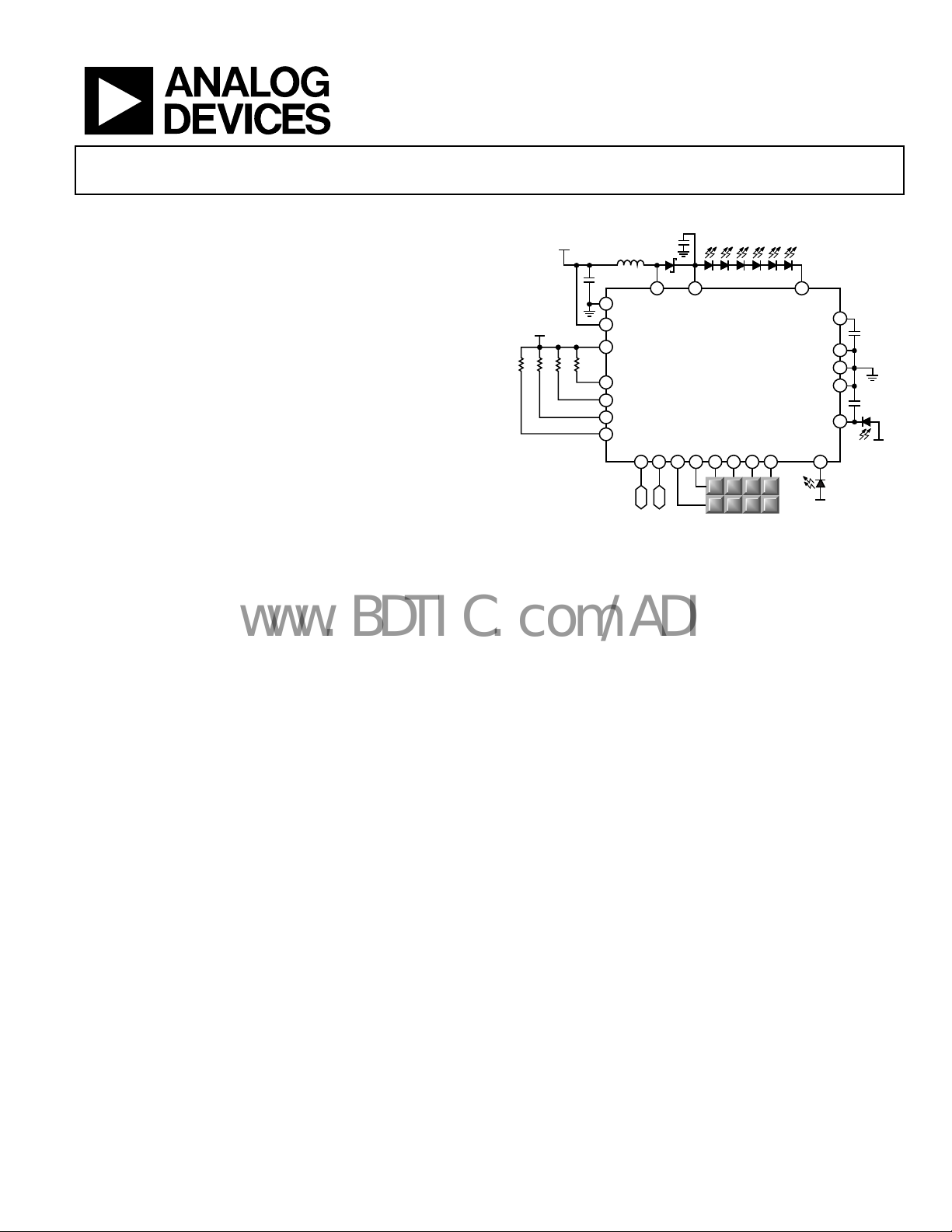
TYPICAL OPERATING CIRCUIT
VBAT
10kΩ
1µF
1
21
16
2.2kΩ
2.2kΩ
5
4
3
15
1µF
4.7µH
2SW22
PGND
VBAT
VDDIO
SCL
SDA
nINT
nRST
13R36R27R18R09C010C111C212
BST
ADP5520
I/O
I/O
ABCD
EFGH
Figure 1.
ADP5520
23
BL_SNK
GND
GND
GND
CMP_IN
ILED
14
VBAT
20
19
18
24
17
CAP_OUT
C3
1µF
100nF
VBAT
7445-001
APPLICATIONS
Display backlight driver for phones that require slider or flip
keypad functions with single or multiple LED indicators
GENERAL DESCRIPTION
The ADP5520 is a versatile single-chip, white LED backlight
driver with a user configurable I/O expander. This device fits
handset applications where the flip or slider section of the phone
requires backlighting, I/O signaling and detecting, auxiliary LED
lighting, and keypad functions. By incorporating an I
compatible serial interface and a single line interrupt, the
ADP5520 significantly reduces the total number of lines
required to interface with the baseband processor across the
hinge flex.
2
C®-
The ADP5520 can detect ambient light levels and adjust the
backlight brightness accordingly, resulting in extended battery
operation.
Once configured, the ADP5520 is capable of controlling the
flip/slider backlight intensity, on/off timing, dimming, and
fading without the intervention of the main processor, which
results in valuable battery power saving.
Rev. 0
Information furnished by Analog Devices is believed to be accurate and reliable. However, no
responsibility is assumed by Analog Devices for its use, nor for any infringements of patents or other
rights of third parties that may result from its use. Specifications subject to change without notice. No
license is granted by implication or otherwise under any patent or patent rights of Analog Devices.
Trademarks and registered trademarks are the property of their respective owners.
One Technology Way, P.O. Box 9106, Norwood, MA 02062-9106, U.S.A.
Tel: 781.329.4700 www.analog.com
Fax: 781.461.3113 ©2008 Analog Devices, Inc. All rights reserved.
Page 2

ADP5520
www.BDTIC.com/ADI
TABLE OF CONTENTS
Features .............................................................................................. 1
Applications ....................................................................................... 1
Typical Operating Circuit ................................................................ 1
General Description ......................................................................... 1
Revision History ............................................................................... 2
Specifications ..................................................................................... 3
I2C Timing Specifications ............................................................ 4
Absolute Maximum Ratings ............................................................ 5
Thermal Resistance ...................................................................... 5
ESD Caution .................................................................................. 5
Pin Configuration and Function Descriptions ............................. 6
Typical Performance Characteristics ............................................. 7
Theory of Operation ........................................................................ 9
Backlight Drive and Control ....................................................... 9
Backlight Operating Levels ....................................................... 10
Backlight Maximum and Dim Settings ................................... 10
Backlight Turn On/Off/Dim ..................................................... 11
Automatic Dim and Turn Off Timers ..................................... 11
Linear Backlight Fade In and Fade Out ................................... 12
Fade Override ............................................................................. 13
Advanced Fading (Square) ........................................................ 13
Advanced Fading (Cubic 1 and Cubic 2) ................................ 14
Ambient Light Sensing .............................................................. 14
Automatic Backlight Adjustment ............................................. 15
I/O Expansion Pins (GPIOs) .................................................... 15
I/O Expansion Pins (Keypad Matrix) ...................................... 15
I/O Expansion Pins and ILED Pin (Auxiliary LED Current
Sinks) ............................................................................................ 17
Interrupt Output (nINT) ........................................................... 19
Reset Input (nRST) .................................................................... 19
Communication Interface ............................................................. 20
Register Map ................................................................................... 21
Detailed Register Descriptions ..................................................... 22
Applications Information .............................................................. 34
Converter Topology ................................................................... 34
PCB Layout ................................................................................. 35
Example Circuits ............................................................................ 36
Outline Dimensions ....................................................................... 38
Ordering Guide .......................................................................... 38
REVISION HISTORY
7/08—Revision 0: Initial Version
Rev. 0 | Page 2 of 40
Page 3

ADP5520
www.BDTIC.com/ADI
SPECIFICATIONS
VBAT = 2.7 V to 4.8 V, TJ = −40°C to +125°C, unless otherwise noted.1
Table 1.
Parameter Symbol Conditions Min Typ Max Unit
SUPPLY VOLTAGE
VBAT Input Voltage Range V
VDDIO Input Voltage Range V
Undervoltage Lockout Threshold UVLO
UVLO
UVLO
UVLO
SW leakage SW
SUPPLY CURRENT
Shutdown Current3 I
Standby Current4 I
BACKLIGHT LED DRIVER (SW, BST)
Current Limit (Peak Inductor Current) 450 600 750 mA
Switch On Resistance 100 200 400 mΩ
Overvoltage Limit 24.5 27 29.5 V
Boost Startup Time 1 ms
BACKLIGHT LED CURRENT SINK (BL_SNK)
Full-Scale Backlight Current 26 30 32 mA
Backlight Current Ramp Rate Fade timers disabled 0.3 mA/ms
AMBIENT LIGHT SENSOR (CMP_IN)
Full-Scale Current BL
INPUT LOGIC LEVELS (SCL, SDA, nRST, C0, C1, C2, C3, R0, R1, R2, R3)5
Logic Low Input Voltage VIL 1.8 V ≤ VDDIO ≤ 3.3 V2 0.3 × VDDIO V
Logic High Input Voltage VIH 1.8 V ≤ VDDIO ≤ 3.3 V2 0.7 × VDDIO V
Input Leakage Current V
INPUT LOGIC DEBOUNCE (nRST, C0, C1, C2, C3, R0, R1, R2, R3)6 V
PUSH-PULL OUTPUT LOGIC LEVELS (C0, C1, C2, C3, R0, R1, R2, R3)7
Logic Low Output Voltage VOL I
Logic High Output Voltage VOH I
OPEN-DRAIN OUTPUT LOGIC LEVELS (nINT, SDA)
Logic Low Output Voltage VOL I
Logic High Leakage Current V
AUX LED CURRENT SINK (ILED, C3, R3)8
Leakage LED
Full-scale Current Sink LED
GPIO PULL-UP RESISTANCE (C0, C1, C2, C3, R0, R1, R2, R3)9 50 65 80 kΩ
THERMAL SHUTDOWN
Thermal Shutdown Threshold TS TJ rising 150 °C
Thermal Shutdown Hysteresis TS
1
All limits at temperature extremes are guaranteed via correlation using standard statistical quality control (SQC). Typical values are at T
2
3.3 V or VBAT, whichever is smaller.
3
Internal LDO powered down, digital blocks inactive, I2C inactive, boost inactive.
4
Internal LDO powered up, digital blocks active, I2C active, boost inactive.
5
C0, C1, C2, C3, R0, R1, R2, and R3 are configured as digital inputs.
6
C0, C1, C2, C3, R0, R1, R2, and R3 are configured as digital inputs, with debounce enabled.
7
C0, C1, C2, C3, R0, R1, R2, and R3 are configured as digital outputs.
8
C3 and R3 are configured as digital inputs with pull-up.
9
C0, C1, C2, C3, R0, R1, R2, and R3 are configured as digital inputs with pull-up.
2.7 5.5 V
BAT
1.8 3.32 V
VDDIO
VBAT falling 1.7 2.1 V
VBAT
VBAT rising 2.4 2.7 V
VBAT
VDDIO falling 1.1 1.3 V
VDDIO
VDDIO rising 1.4 V
VDDIO
0.1 1 A
LEAKAGE
VDDIO = 0 V 0.1 1 A
SD
1.8 V ≤ VDDIO ≤ 3.3 V2,
STNBY
25 45 A
nSTNBY = 0
0.7 1 1.2 mA
FULLSCALE
1.8 V ≤ VDDIO ≤ 3.3 V2 0.1 1 µA
I-LEAKAGE
50 75 100 µs
IL-DBNC
= 1 mA 0.4 V
SINK
= 1 mA VDDIO − 0.2 V
SOURCE
= 1 mA 0.4 V
SINK
1.8 V ≤ VDDIO ≤ 3.3 V2 0.1 1 µA
OH-LEAKAGE
Sink disabled 0.1 1 µA
LEAKAGE
Applied pin voltage = 1 V 10.5 14 16.5 mA
FULLSCALE
T
HYS
falling 10 °C
J
= 25⁰C, VBAT = 3.6 V.
A
Rev. 0 | Page 3 of 40
Page 4
ADP5520
www.BDTIC.com/ADI
I2C TIMING SPECIFICATIONS
Table 2.
Parameter Description Min Max Unit
Delay from Reset Deassertion to I2C Access 60 s
f
SCL clock frequency 400 kHz
SCL
t
SCL high time 0.6 s
HIGH
t
SCL low time 1.3 s
LOW
t
Data setup time 100 ns
SU, DAT
t
Data hold time 0 0.9 s
HD, DAT
t
Setup time for repeated start 0.6 s
SU, STA
t
Hold time for start/repeated start 0.6 s
HD, STA
t
Bus free time for stop and start condition 1.3 s
BUF
t
Setup time for stop condition 0.6 s
SU, STO
tR Rise time for SCL and SDA 20 + 0.1 CB 300 ns
tF Fall time for SCL and SDA 20 + 0.1 CB 300 ns
tSP Pulse width of suppressed spike 0 50 s
1
C
Capacitive load for each bus line 400 pF
B
1
CB is the total capacitance of one bus line in picofarads.
SDA
t
t
LOW
SCL
S
S = START CONDI TION
Sr = REPEATED START CONDITION
P = STOP CO NDITION
t
R
t
HD, DAT
t
SU, DAT
t
HIGH
Figure 2. I
t
F
t
F
t
SU, STA
2
C Interface Timing Diagram
Sr P S
t
HD, STA
t
SP
t
SU, STO
BUF
t
R
07445-002
Rev. 0 | Page 4 of 40
Page 5

ADP5520
www.BDTIC.com/ADI
ABSOLUTE MAXIMUM RATINGS
Table 3.
Parameter Rating
VBAT to GND −0.3 V to +6 V
VDDIO to GND −0.3 V to VBAT
SW, BST to GND −0.3 V to +30 V
ILED, R0, R1, R2, R3, C0, C1, C2, C3, CMP_IN,
−0.3 V to +6 V
SCL, SDA, nINT, nRST, CAP_OUT, BL_SNK
to GND
PGND to GND −0.3 V to +0.3 V
Operating Ambient Temperature Range −40°C to +85°C1
Operating Junction Temperature Range −40°C to +125°C
Storage Temperature Range −65°C to +150°C
Soldering Conditions JEDEC J-STD-020
1
In applications where high power dissipation and poor thermal resistance
are present, the maximum ambient temperature may have to be derated.
Maximum ambient temperature (T
operating junction temperature (T
dissipation of the device (PD
resistance of the part/package in the application (θ
equation: T
A(MAX)
= T
J(MAXOP)
(MAX)
− (θJA × P
) is dependent on the maximum
A(MAX)
= 125°C), the maximum power
J(MAXOP)
), and the junction-to-ambient thermal
).
D(MAX)
), using the following
JA
THERMAL RESISTANCE
θJA is specified for the worst-case conditions, that is, a device
soldered in a circuit board for surface-mount packages.
Table 4. Thermal Resistance
Package Type θJA Unit
24-Lead LFCSP (CP-24-2) 50 °C/W
ESD CAUTION
Stresses above those listed under Absolute Maximum Ratings
may cause permanent damage to the device. This is a stress
rating only; functional operation of the device at these or any
other conditions above those indicated in the operational
section of this specification is not implied. Exposure to absolute
maximum rating conditions for extended periods may affect
device reliability.
Absolute maximum ratings apply individually only, not in
combination. Unless otherwise specified, all other voltages are
referenced to GND.
Rev. 0 | Page 5 of 40
Page 6

ADP5520
www.BDTIC.com/ADI
PIN CONFIGURATION AND FUNCTION DESCRIPTIONS
VBAT
BST
BL_SNK
GND
CAP_OUT
GND
20
19
21
22
23
24
PIN 1
INDICATOR
1PGND
2SW
3nINT
ADP5520
4SDA
TOP VIEW
5SCL
(Not to Scal e)
6R2
9
7
8
R0
C0
NOTES
1. EXPOSED PAD MUST BE CONNE CTED
TO GROUND.
R1
Figure 3. Pin Configuration
Table 5. Pin Function Descriptions
Pin No. Mnemonic Description
1 PGND Power Switch Output to Ground.
2 SW Power Switch Input.
3 nINT Processor Interrupt. This pin is active low, open drain, and should be pulled up to VDDIO.
4 SDA I2C-Compatible Serial Data Line. Open drain requires external pull-up to VDDIO.
5 SCL I2C-Compatible Serial Clock Line. Open drain requires external pull-up to VDDIO.
6 R2 Row 2 when configured in a keypad matrix, D2 when configured as an I/O.
7 R1 Row 1 when configured in a keypad matrix, D1 when configured as an I/O.
8 R0 Row 0 when configured in a keypad matrix, D0 when configured as an I/O.
9 C0 Column 0 when configured in a keypad matrix, D4 when configured as an I/O.
10 C1 Column 1 when configured in a keypad matrix, D5 when configured as an I/O.
11 C2 Column 2 when configured in a keypad matrix, D6 when configured as an I/O.
12 C3 Column 3 when configured in a keypad matrix, D7 when configured as an I/O, LED 2 when configured as a current sink.
13 R3 Row 3 when configured in a keypad matrix, D3 when configured as an I/O, LED 3 when configured as a current sink.
14 ILED LED 1 Current Sink.
15 nRST
Reset Input, Active Low. This input signal resets the device to the power-up default conditions. Must be driven low
for 75 µs (typical) to be valid.
16 VDDIO
Supply Voltage for the I/O Pins. Voltage is 1.8 V to 3.3 V (or VBAT, whichever is smaller). If VDDIO = 0, the device goes
into full shutdown mode.
17 CMP_IN Input for Ambient Light Sensing.
18 GND Ground.
19 GND Ground.
20 CAP_OUT
Capacitor for Internal 2.7 V LDO. A 1 F capacitor must be connected between this pin and GND. Do not use this
pin to supply external loads.
21 VBAT Main Supply Voltage for the IC (2.7 V to 5.5 V).
22 BST Overvoltage Monitor Input for the Boost Converter.
23 BL_SNK Backlight Current Sink.
24 GND Ground.
18 G ND
17 CMP_IN
16 V DDIO
15 n RST
14 ILE D
13 R3
11
12
10
C2
C3
C1
07445-003
Rev. 0 | Page 6 of 40
Page 7

ADP5520
www.BDTIC.com/ADI
TYPICAL PERFORMANCE CHARACTERISTICS
VBAT = 3.6 V, TA = 25°C, unless otherwise noted. Inductor = LPS4012-472MLB. Schottky rectifier = MBR140SFT1G.
90
85
80
75
70
65
60
EFFICIE NCY (%)
55
50
45
40
024681012141618202224262830
BACKLIGHT CURRENT (mA)
6 LEDs, VBAT = 3. 0V
6 LEDs, VBAT = 3. 6V
6 LEDs, VBAT = 4. 2V
6 LEDs, VBAT = 5. 5V
Figure 4. Efficiency vs. Backlight Current (6 LEDS)
07445-047
48
40
TEMP = +25°C
32
24
16
8
STANDBY SUPPLY CURRENT (µA)
0
2.5 3.0 3.5 4.0 4.5 5.0 5.5 6.0
TEMP = –40°C
TEMP = +85°C
VBAT (V)
Figure 7. Standby Supply Current vs. VBAT
07445-050
90
85
80
75
70
65
60
EFFICIE NCY (%)
55
50
45
40
024681012141618202224262830
BACKLIGHT CURRENT (mA)
6 LEDs, VBAT = 3. 6V
5 LEDs, VBAT = 3. 6V
4 LEDs, VBAT = 3. 6V
Figure 5. Efficiency vs. Backlight Current (4, 5, and 6 LEDS)
90
85
80
75
70
65
60
EFFICIE NCY (%)
55
50
45
40
024681012141618202224262830
BACKLIGHT CURRENT (mA)
6 LEDs, VBAT = 4.2V
6 LEDs, VBAT = 4.2V,
AUTOLOAD-ENABLED
Figure 6. Efficiency vs. Backlight Current (Autoload On/Off)
16
14
12
10
8
6
4
2
AUX LED FULL -SCALE SINK CURRENT (mA)
0
0 0.5 1.0 1.5 2.0 2.5 3.0
07445-048
AUX LED PIN VO LTAGE (V)
07445-051
Figure 8. Typical Auxiliary LED Pin (R3, C3, or ILED), Full-Scale Sink Current vs.
Applied Pin Voltage
07445-049
Rev. 0 | Page 7 of 40
Page 8
ADP5520
www.BDTIC.com/ADI
SW
1
INDUCTOR CURRENT
2
BST
BL_SNK
3
4
CH1 20.0V
CH3 10.0V
CH2 500mA
CH4 1.0V
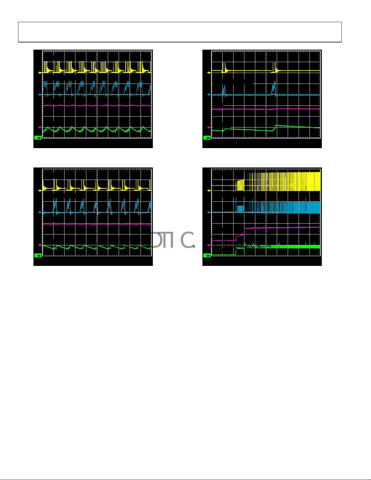
Figure 9. Boost Operation (Backlight = 30 mA)
SW
1
INDUCTOR CURRENT
2
BST
TIME (4µs/DIV)
SW
1
INDUCTOR CURRENT
2
BST
BL_SNK
3
4
CH1 20.0V
07445-052
CH3 10.0V
CH2 500mA
CH4 1.0V
TIME (4µs/DIV)
07445-054
Figure 11. Boost Operation (Backlight = 2 mA)
SW
1
INDUCTOR CURRENT
2
BST
BL_SNK
3
4
CH1 20.0V
CH3 10.0V
CH2 500mA
CH4 1.0V
Figure 10. Boost Operation (Backlight = 15 mA)
TIME (4µs/DIV)
07445-053
3
4
BL_SNK
CH1 10.0V
CH3 10.0V
CH2 500mA
CH4 1.0V
TIME (1ms/DIV)
Figure 12. Boost Startup
07445-055
Rev. 0 | Page 8 of 40
Page 9
ADP5520
www.BDTIC.com/ADI
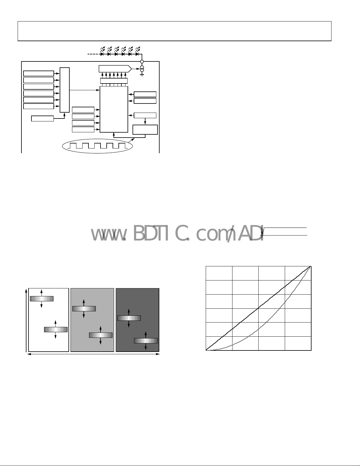
THEORY OF OPERATION
VBAT
1µF
4.7µH
1µF
PGND
VBAT
VDDIO
CAP_OUT
1µF
SCL
SDA
nINT
nRST
1
21
16
20
5
4
3
15
GND GND GND
2
POR
INTERFACE
ADP5520
1918 24
SW
I-LIMIT
BOOST
CONTROL
IN
EN
LDO
OUT
2.7V
BIAS/CLOCK
I/O CONF IG
GPIO/KEYPAD
6R27R18R09C010C111
27V
THERMAL S/D
Figure 13. Internal Block Diagram
The ADP5520 is a backlight white LED driver with an I/O port
expander. It is ideal for cell phone designs and other portable
devices, where keypad and/or extended I/O functionality is
needed. Programmable fade-in, fade-out, dim, and off timers
provide the backlight with flexible control features. Using an
external photodiode, the ADP5520 can perform ambient light
sensing, and adjust the backlight brightness according to
varying lighting conditions.
The I/O port expander has eight configurable GPIO pins. The
I/Os can be configured as a keypad matrix, digital inputs, or
digital outputs. Additionally, two of the I/Os (R3 and C3) can be
configured as current sink lines and, paired with a dedicated
sink line (ILED), can be used to drive up to three auxiliary LEDs.
Programmable fading is also available for auxiliary LEDs.
Once programmed through its I
2
C-compatible interface, the
ADP5520 can run autonomously. An interrupt line (nINT) is
available to alert an external microprocessor of the status of its
I/Os, keypad presses and releases, ambient light sensor comparator
states, and overvoltage conditions.
BST BL_SNK
22
AUTO
LOAD
OVP
STATE MACHINE
REGISTER MAP
INTERRUPT/ RESET
CONTROL
13
R3
C2
FB
BACKLIGHT
CURRENT
CONTROL
12
C3
ILED
14
BACKLIGHT DRIVE AND CONTROL
White LEDs are common in backlighting the displays of modern
portable devices such as cell phones. White LEDs require a high
forward voltage, V
Display panels, depending on their size, can be backlit with
single or multiple white LEDs. In panels that require multiple
LEDs, the LEDs are commonly connected in a series string to
achieve uniform brightness in each LED by passing a common
current through all of them. The LED string needs to be biased
with a voltage greater than the sum of the V
before it conducts.
The ADP5520 is an asynchronous boost converter capable of
driving an LED string with 24.5 V (minimum). For detailed
information about the boost device, see the Applications
Information section. With sufficient forward voltage created,
the ADP5520 controls the current (and thus the brightness)
of the LED string via an adjustable internal current sink. An
internal state machine, in conjunction with programmable
timers, dynamically adjusts the current sink between 0 mA
and 30 mA to achieve impressive backlight control features.
23
0.65V
VBAT
100nF
07445-004
of each LED
F
LIGHT
SENSOR
LED
CURRENT
CONTROL
, before they conduct current and emit light.
F
17
CMP_IN
Rev. 0 | Page 9 of 40
Page 10
ADP5520
A
Y
www.BDTIC.com/ADI
BACKLIGHT MAXIMUM AND DIM SETTINGS
The backlight maximum and dim current settings are determined by a 7-bit code programmed by the user into the registers
listed in the Backlight Operating Levels section. This 7-bit
resolution allows the user to set the backlight to 1 of 128
different levels between 0 mA and 30 mA. The ADP5520 can
implement two distinct algorithms to achieve a linear and a
nonlinear relationship between input code and backlight
current. The BL_LAW bits in Register 0x02 are used to swap
between algorithms.
By default, the ADP5520 uses a linear algorithm (BL_LAW =
00), where backlight current increases linearly for a corresponding increase of input code. Backlight current (in mA) is determined
by the following equation:
Backlight Current = Code × (Fullscale_Current/127) (1)
where:
Code is the input code programmed by the user.
Fullscale_Current is the maximum sink current allowed
(typically 30 mA).
The ADP5520 can also implement a nonlinear (square approximation) relationship between input code and backlight current level.
In this case (BL_LAW = 01), the backlight current (in mA) is
determined by the following equation:
2
⎞
⎟
⎟
⎠
07445-007
Backlight Current =
⎛
⎜
×
Code (2)
⎜
⎝
127
CurrentFullscale
_
Figure 16 shows the backlight current level vs. input code for
both the linear and square law algorithms.
30
25
20
15
10
BACKLIGHT CURRENT (mA)
5
0
0 32 64 96 128
LINEAR
SQUARE
SINK CODE
Figure 16. Backlight Current vs. Sink Code
DAYLIGHT_MAX
DAYLIGHT_DIM
OFFICE_MAX
OFFICE_DIM
DARK_MAX
DARK_DIM
BL_LVL
MUX
BST
BL_OFFT
BL_DIMT
BL_FI
BL_FO
BL_VALUE
COUNTERS
AND
CONTROL
LOGIC
BL_SNK
BL_EN
DIM_EN
BL_LAW
CLOCK
GENERATOR
Figure 14. Backlight Brightness Control
BACKLIGHT OPERATING LEVELS
Backlight brightness control can operate in three distinct levels:
daylight (L1), office (L2), and dark (L3). The BL_LVL bits in
Register 0x02 control the level in which the backlight operates.
The BL_LVL bits can be changed manually, or if in automatic
mode, by the ambient light sensor (see the Ambient Light Sensing
section). By default, the backlight operates at daylight level
(BL_LVL = 00), where the maximum brightness is set using
Register 0x05 (DAYLIGHT_MAX). A daylight dim setting can
also be set using Register 0x06 (DAYLIGHT_DIM). When operating at office level (BL_LVL = 01), the backlight maximum and
dim brightness settings are set by Register 0x07 (OFFICE_MAX)
and Register 0x08 (OFFICE_DIM). When operating at dark
level (BL_LVL = 10), the backlight maximum and dim brightness
settings are set by Register 0x09 (DARK_MAX) and Register 0x0A
(DARK_DIM).
D
30mA
BACKLIGHT CURRENT
0
LIGHT ( L1) OFFICE (L2) DARK (L3)
DAYLIGHT_MAX
OFFICE_MAX
DARK_MAX
DAYLIGHT_DIM
OFFICE_DIM
DARK_DIM
BACKLIGHT OPERATING LEVELS
Figure 15. Backlight Operating Levels
07445-005
07445-006
Rev. 0 | Page 10 of 40
Page 11
ADP5520
www.BDTIC.com/ADI
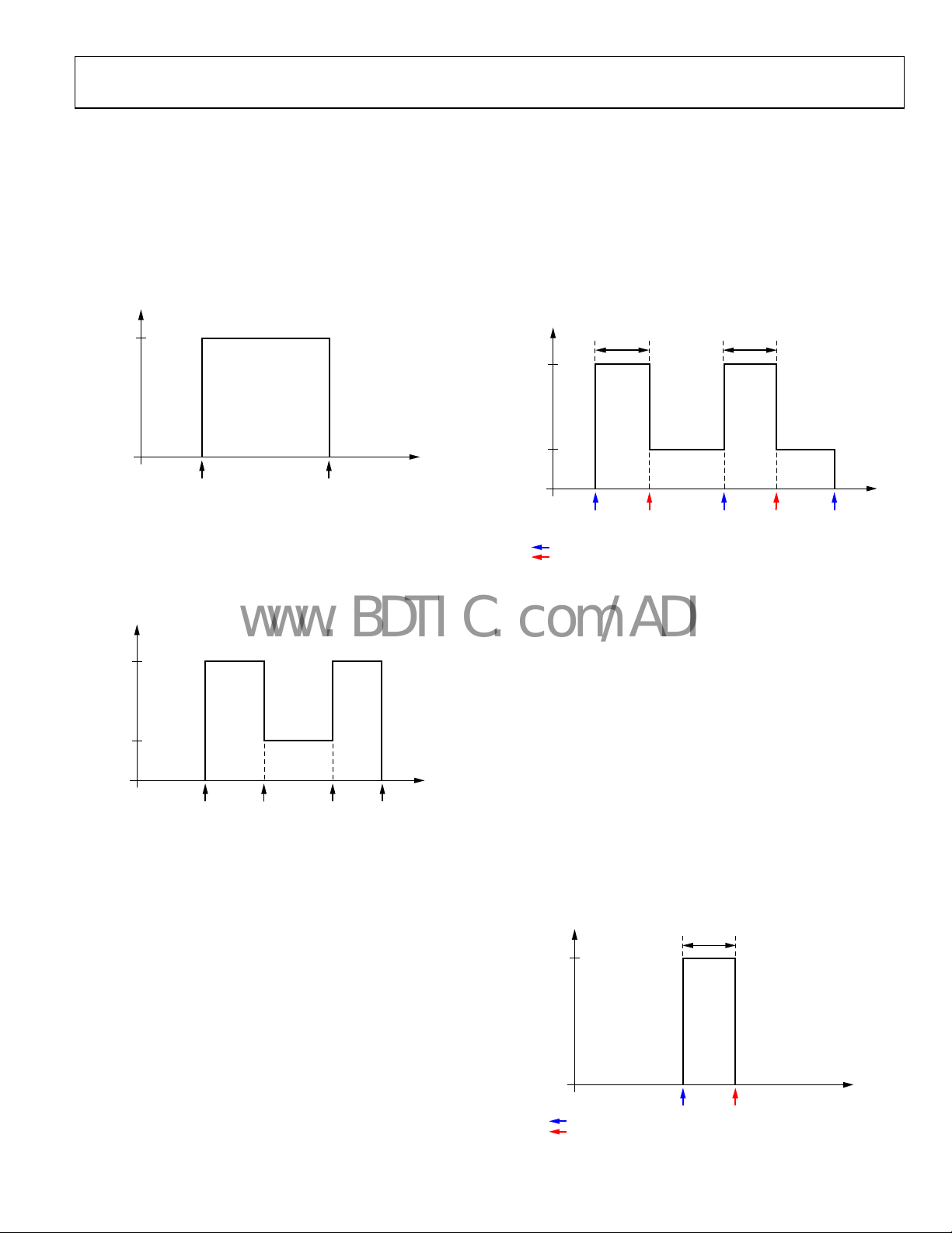
BACKLIGHT TURN ON/OFF/DIM
With the device in operating mode (nSTNBY = 1), the backlight
can be turned on using the BL_EN bit in Register 0x00. Before
turning on the backlight, the user should choose which level
(daylight (L1), office (L2), or dark (L3)) to operate in, and ensure
that maximum and dim settings are programmed for that level.
The backlight turns on when BL_EN = 1. The backlight turns
off when BL_EN = 0.
BACKLIGHT
CURRENT
MAX
AUTOMATIC DIM AND TURN OFF TIMERS
The user can program the backlight to dim automatically by
using the BL_DIMT timer in Register 0x03. The dim timer has
15 settings ranging from 10 sec to 2 min. The user should
program the dim timer before turning on the backlight. If
BL_EN = 1, the backlight turns on to its maximum setting, and
the dim timer starts counting. When the dim timer expires, the
internal state machine sets DIM_EN = 1, and the backlight goes
to its dim setting.
BACKLIGHT
CURRENT
MAX
DIM
DIM TIME R
RUNNING
DIM TIMER
RUNNING
BL_EN = 1 BL_EN = 0
Figure 17. Backlight Turn On/Off
07445-008
While the backlight is on (BL_EN = 1), the user can make it
change to a dim setting by programming DIM_EN = 1 in
Register 0x00. If DIM_EN = 0, the backlight reverts to its
maximum setting.
BACKLIGHT
CURRENT
MAX
DIM
BL_EN = 1
Figure 18. Backlight Turn On/Dim/Off
DIM_EN = 1 DIM_EN = 0 BL_EN = 0
07445-009
The maximum and dim settings can be set between 0 mA and
30 mA; therefore, it is possible to program a dim setting that is
greater than a maximum setting. For normal expected operation,
users should ensure that the dim setting is programmed to be less
than the maximum setting.
It is also possible to activate the backlight automatically when a
key press is detected. With the row and column pins configured as
a keypad matrix, and the KP_BL_EN bit asserted in Register 0x02,
the internal state machine asserts BL_EN and turns on the backlight if a key is pressed. See the I/O Expansion Pins (Keypad
Matrix) section for more information on using keypad
functionality.
BL_EN = 1
SET BY USER
SET BY INTERNAL STATEMACHINE
Figure 19. Dim Timer
BL_EN = 1
OR
DIM_EN = 1
BL_EN = 0DIM_EN = 1 DIM_EN = 0
If the user clears the DIM_EN bit (or reasserts the BL_EN bit),
the backlight reverts to its maximum setting and the dim timer
begins counting again. When the dim timer expires, the internal
state machine again sets DIM_EN = 1, and the backlight goes to
its dim setting. Reasserting BL_EN at any point during the dim
timer countdown causes the timer to reset and begin counting
again. The backlight can be turned off at any point during the
dim timer countdown by clearing BL_EN.
The user can also program the backlight to turn off automatically by using the BL_OFFT timer in Register 0x03. The off
timer has 15 settings ranging from 10 sec to 2 min. The user
should program the off timer before turning on the backlight.
If BL_EN = 1, the backlight turns on to its maximum setting,
and the off timer starts counting. When the off timer expires,
the internal state machine clears the BL_EN bit, and the
backlight turns off.
BACKLIGHT
CURRENT
MAX
OFF TIMER
RUNNING
07445-010
Rev. 0 | Page 11 of 40
SET BY USER
SET BY INTERNAL STATE MACHINE
BL_EN = 1 BL_EN = 0
Figure 20. Off Timer
07445-011
Page 12

ADP5520
A
www.BDTIC.com/ADI
Reasserting BL_EN at any point during the off timer countdown
causes the timer to reset and begin counting again. The backlight
can be turned off at any point during the off timer countdown
by clearing BL_EN.
The dim timer and off timer can be used together for sequential
maximum-to-dim-to-off functionality. With both the dim and
off timers programmed, if BL_EN is asserted, the backlight turns
on to its maximum setting. When the dim timer expires, the
backlight changes to its dim setting. When the off timer expires,
the backlight turns off.
BACKLIGHT
CURRENT
MAX
DIM
SET BY USER
SET BY INTERNAL STATE MACHINE
DIM TIMER
RUNNING
OFF TIMER
RUNNING
BL_EN = 1 BL _EN = 0DIM_EN = 1
Figure 21. Dim and Off Timers Used Together
LINEAR BACKLIGHT FADE IN AND FADE OUT
To counteract the abrupt visual effect of near instant turn-on
and turn-off of the backlight, the ADP5520 contains timers to
facilitate the smooth fading between off, on, and dim states. By
default (BL_LAW = 00), the ADP5520 implements a fading
scheme using the linear backlight code algorithm (see Equation 1).
The BL_FI timer in Register 0x04 can be used for smooth fade-in
transitions from low to high backlight settings, such as off-to-dim,
off-to-maximum, and dim-to-maximum. The BL_FI timer can be
programmed to one of 15 settings ranging from 0.3 sec to 5.5 sec.
The BL_FI timer should be programmed before asserting BL_EN.
30.0
27.5
25.0
22.5
20.0
17.5
15.0
12.5
10.0
7.5
BACKLIGHT CURRENT (mA)
5.0
2.5
0
0 0.5 1.0 1.5 2.0 2.5 3.0 3.5 4.0 4.5 5.0 5.5
FADE-IN TIME (s)
Figure 22. Linear Fade-In Times
0.3 SEC
0.6 SEC
0.9 SEC
1.2 SEC
1.5 SEC
1.8 SEC
2.1 SEC
2.4 SEC
2.7 SEC
3.0 SEC
3.5 SEC
4.0 SEC
4.5 SEC
5.0 SEC
5.5 SEC
07445-013
Rev. 0 | Page 12 of 40
07445-012
The time programmed in BL_FI represents the time it takes the
backlight current to go from 0 mA to 30 mA. Fading between
intermediate settings is shorter.
The BL_FO timer in Register 0x04 can be used for smooth fadeout transitions from high to low backlight settings such as
maximum-to-dim and dim-to-off. The BL_FO timer can be
programmed to one of 15 settings ranging from 0.3 sec to 5.5 sec.
The BL_FO timer should be programmed before asserting BL_EN.
30.0
27.5
25.0
22.5
20.0
17.5
15.0
12.5
10.0
7.5
BACKLIGHT CURRENT (mA)
5.0
2.5
0
0 0.51.01.52.02.53.03.54.04.55.05.5
FADE-OUT TI ME (s)
Figure 23. Linear Fade-out Times
0.3 SEC
0.6 SEC
0.9 SEC
1.2 SEC
1.5 SEC
1.8 SEC
2.1 SEC
2.4 SEC
2.7 SEC
3.0 SEC
3.5 SEC
4.0 SEC
4.5 SEC
5.0 SEC
5.5 SEC
07445-014
The time programmed in BL_FO represents the time it takes
the backlight current to go from 30 mA to 0 mA. Fading
between intermediate settings is shorter.
Figure 24 shows the fade timers in use. With BL_FI and BL_FO
programmed, if BL_EN is asserted, then the backlight fades in
to its maximum setting. If DIM_EN is asserted, then the backlight
fades out to its dim setting. If BL_EN is cleared, the backlight
fades out to off.
F
BACKLIGHT
CURRENT
FADE -IN
OFF-TO-MAX
MAX
DIM
BL_EN = 1 BL_EN = 0 BL_EN = 0 BL_EN = 0
DIM_EN = 1
SET BY USER
DE-OUT
MAX-TO-DIM
FADE-OUT
DIM-TO-OF F
FADE-OUT FADE-I N
FADE -OU TFADE-IN
BL_EN = 1 BL_EN = 1
Figure 24. Backlight Turn On/Off/Dim with Fade Timers
During any point in a fade-out, if BL_EN is asserted, then the
backlight stops at its current fade-out position and begins
fading in.
The fade-in and fade-out timers can be used independently of each
other, that is, fade-in can be enabled while fade-out is disabled.
The fade timers can also be used with the off and dim timers.
07445-015
Page 13

ADP5520
www.BDTIC.com/ADI
Figure 25 shows the fade timers used with the dim and off timers.
BACKLIGHT
CURRENT
MAX
DIM
BL_EN = 1 BL_EN = 0
SET BY USER
SET BY INTERNAL STATE MACHINE
FADE -IN
DIM TIMER
RUNNING
DIM_EN = 1
FADE-OUT
OFF TIMER
RUNNING
FADE-OUT
DIM_EN = 0
Figure 25. Fade/Dim/Off Timers Used Together
FADE OVERRIDE
A fade override feature allows the BL_FI and BL_FO timers to
be overridden if the BL_EN bit is reasserted (either by the user
or due to a key press) during a fade-in or fade-out period, and
sets the backlight to its maximum setting. Fade override can be
activated by setting the FOVR bit in Register 0x02.
BACKLIGHT
CURRENT
MAX
BL_EN = 1 BL_EN = 0 BL_EN = 0
SET BY USER
FADE-IN
OVERRIDDEN
BL_EN = 1
(REASSERTED BY
USER OR A KEY PRESS)
Figure 26. Fade Override
FADE-OUT
OVERRIDDEN
BL_EN = 1
(REASSERTED BY
USER OR A KEY PRESS)
07445-016
07445-017
ADVANCED FADING (SQUARE)
Although the default linear fade algorithm gives a smooth increase
and decrease in backlight current, the resulting increase and
decrease in brightness still appears visually abrupt. For example,
for a given fade-in time, the eye can notice an initial increase in
brightness as backlight current is increased, but cannot perceive
much more of an increase in brightness as backlight current is
increased to maximum.
The reason for this is that the eye, like all human senses, perceives
changes in light when the brightness of the light source is changed
logarithmically (Weber-Fechner law). To achieve a more natural
fading experience to the user, the fade timers can be used in
conjunction with the square law approximation backlight codes
(see Equation 2) by setting BL_LAW = 01.
30.0
27.5
25.0
22.5
20.0
17.5
15.0
12.5
10.0
7.5
BACKLIGHT CURRENT (mA)
5.0
2.5
0
0 0.5 1.0 1.5 2.0 2.5 3.0 3.5 4.0 4.5 5.0 5.5
FADE-IN TIME (s)
0.3 SEC
0.6 SEC
0.9 SEC
1.2 SEC
1.5 SEC
1.8 SEC
Figure 27. Square Law Fade-In Times
30.0
27.5
25.0
22.5
20.0
17.5
15.0
12.5
10.0
7.5
BACKLIGHT CURRENT (mA)
5.0
2.5
0
0 0.51.01.52.02.53.03.54.04.55.05.5
FADE-O UT TI ME (s)
Figure 28. Square Law Fade-Out Times
2.1 SEC
2.4 SEC
2.7 SEC
3.0 SEC
3.5 SEC
4.0 SEC
4.5 SEC
5.0 SEC
5.5 SEC
0.3 SEC
0.6 SEC
0.9 SEC
1.2 SEC
1.5 SEC
1.8 SEC
2.1 SEC
2.4 SEC
2.7 SEC
3.0 SEC
3.5 SEC
4.0 SEC
4.5 SEC
5.0 SEC
5.5 SEC
07445-018
07445-019
Rev. 0 | Page 13 of 40
Page 14

ADP5520
www.BDTIC.com/ADI
ADVANCED FADING (CUBIC 1 AND CUBIC 2)
Two additional advanced techniques are available for fading the
backlight brightness levels, Cubic 1 (BL_LAW = 10) and Cubic 2
(BL_LAW = 11). Referring to the backlight brightness control
block diagram shown in Figure 14, linear and square fading is
implemented by ramping the 128 linear/square algorithm codes
at a fixed frequency over the duration of a given fade-in/fadeout time.
Cubic fading is implemented by reusing the square algorithm
codes, but by ramping them with a clock source whose frequency
output increases as the sink current code increases (see Figure 29).
Cubic 1 and Cubic 2 differ by having separate frequency vs.
code characteristics.
BST
DAYLIGHT_MAX
DAYLIGHT_DIM
OFFICE _MAX
OFFICE_DIM
DARK_MAX
DARK_DIM
BL_LVL
MUX
BL_OFFT
BL_DIMT
BL_FI
BL_FO
BL_VALUE
COUNTERS
AND
CONTROL
LOGIC
Figure 29. Backlight Brightness Control (Cubic)
Figure 30 shows a comparison of fade law techniques. Cubic
fades complete faster than linear or square fades for a given fade
time setting. Cubic 1 completes approximately 30% faster, and
Cubic 2 completes approximately 10% faster than an equivalent
linear or square fade time.
With four fade laws and 15 fade time settings, users have tremendous flexibility to find the right fade experience for their application.
30
25
20
15
10
BACKLIGHT CURRENT (mA)
5
0
0 0.2 0.4 0.6 0.8 1.0
LINEAR
Figure 30. Fade Law Comparison Over a Unit Fade Time
CUBIC 1
CUBIC 2
UNIT FADE TIME
BL_EN
DIM_EN
BL_LAW
CLOCK
GENERATOR
SQUARE
BL_SNK
07445-021
07445-020
AMBIENT LIGHT SENSING
The ADP5520 can be used in conjunction with an external
photosensor to detect when ambient light conditions have
dropped below programmable set points. An ADC samples the
output of the external photosensor. The ADC result is fed into
two programmable trip comparators. The ADC has an input
range of 0 µA to 1000 µA (typical).
L2_EN
L2_TRIP
L2_HYS
FILTER
PHOTO
SENSOR
OUTPUT
ADC
SETTINGS
L3_TRIP
L3_HYS
L3_EN
Figure 31. Ambient Light Sensing and Trip Comparators
The Level 2 (office) light sensor comparator, L2_CMPR, is used
to detect when the photosensor output has dropped below the
programmable L2_TRIP point. If this event occurs, the
L2_OUT status signal is set. L2_CMPR contains programmable
hysteresis, meaning that the photosensor output must rise above
L2_TRIP + L2_HYS before L2_OUT is cleared. L2_CMPR is
enabled in Register 0x0C via the L2_EN bit. The L2_TRIP and
L2_HYS values of L2_CMPR can be set between 0 µA and 1000 µA
(typical) in steps of 4 µA (typical).
L3_CMPR is used to detect when the photosensor output
has dropped below the programmable L3_TRIP point. If this
event occurs, the L3_OUT status signal is set. L3_CMPR contains
programmable hysteresis, meaning that the photosensor output
must rise above L3_TRIP + L3_HYS before L3_OUT is cleared.
L3_CMPR is enabled in Register 0x0C via the L3_EN bit. The
L3_TRIP and L3_HYS values of L3_CMPR can be set between 0
µA and 127 µA (typical) in steps of 0.5 µA (typical).
L2_TRIP
L2_HYS
L3_TRIP
L3_HYS
1 10 100 1000
ADC RANGE (µA)
Figure 32. Comparator Ranges
The L2_CMPR and L3_CMPR comparators can be enabled
independently of each other. The ADC and comparators run
continuously when L2_EN and/or L3_EN are set, during
automatic backlight adjustment mode. A single conversion
L2_OUT
L3_OUT
07445-023
07445-022
Rev. 0 | Page 14 of 40
Page 15

ADP5520
V
G
www.BDTIC.com/ADI
takes 80 ms (typical). Filter times of between 80 ms and 10 sec
can be programmed for the comparators before they change state.
It is also possible to use the light sensor comparators in a single
shot mode. After the single shot measurement is completed, the
internal state machine clears the FORCE_RD bit.
The interrupt flag, CMPR_INT, is set in Register 0x00 if either
of the L2_OUT or L3_OUT status bits change state, meaning
interrupts can be generated if ambient light conditions transition
between any of the programmed trip points. CMPR_INT can
cause the nINT pin to be asserted if the CMPR_IEN bit is set in
Register 0x00. The CMPR_INT flag can be cleared only by
writing a 1 to it.
AUTOMATIC BACKLIGHT ADJUSTMENT
The ambient light sensor comparators can be used to automatically transition the backlight between one of its three operating
levels. To enable this mode, the BL_AUTO_ADJ bit is set in
Register 0x02.
Once enabled, the internal state machine takes control of the
BL_LVL bits and changes them based on the L2_OUT and
L3_OUT status bits. The L2_OUT status bit indicates that ambient
light conditions have dropped below the L2_TRIP point and the
backlight should be moved to its office (L2) level. The L3_OUT
status bit indicates that ambient light conditions have dropped
below the L3_TRIP point and the backlight should be moved
to its dark (L3) level. Table 6 shows the relationship between
backlight operation and the ambient light sensor comparator
outputs.
The L3_OUT status bit has greater priority, so the backlight
operates at L3 (dark) even if L2_OUT is set.
Table 6. Comparator Output Truth Table (X = Don’t Care)
BL_AUTO_ADJ L3_OUT L2_OUT Backlight Operation
0 X X
BL_LVL can be manually
set by the user
1 0 0
BL_LVL = 00, backlight
operates at L1 (daylight)
1 0 1
BL_LVL = 01, backlight
operates at L2 (office)
1 1 0
BL_LVL = 10, backlight
operates at L3 (dark)
1 1 1
BL_LVL = 10, backlight
operates at L3 (dark)
I/O EXPANSION PINS (GPIOs)
The eight I/O expansion pins (R0, R1, R2, R3, C0, C1, C2, and
C3) can be configured as general-purpose digital inputs, digital
inputs with pull-up, or digital outputs. Two of the I/O pins (R3
and C3) are LED current sinks by default. To use them as GPIOs,
set Bit 4 and Bit 5 in Register 0x11. Register 0x17 to Register 0x1F
are used to configure the I/O pins in GPIO mode. Figure 33
shows the typical makeup of a GPIO block, where Rx/Cx
represents any one of the eight I/O lines.
DDIO
Dx_PULL
Dx_IN_DBNC
Dx_IN
Dx_OUT
Dx_DIR
DEBOUNCE
VDDIO
Figure 33. Typical GPIO Block
GPIO (Rx/Cx)
07445-024
When configured as an output, a digital buffer drives the GPIO
Rx and Cx pins to 0 V for a Logic 0 and to the VDDIO rail for a
Logic 1. Output data for each I/O is set using Register 0x1A.
Each I/O has a pull-up resistor that can be enabled when used
as an input. This can be useful for interfacing to an external
signal that has only pull-down capabilities. Pull-ups can be
enabled and disabled using Register 0x1F.
Each I/O has a debounce circuit that effectively filters out glitches
and pulses less than 75 µs (typical) to prevent false triggering
when configured as an input. By default, debounce is enabled
but can be disabled using Register 0x1E.
I/Os configured as inputs store the digital state sensed at each
pin in Register 0x19. Interrupts can be generated by digital
inputs if enabled in Register 0x1B. The input interrupt level
can be selected using Register 0x1D. Interrupts generated are
stored in Register 0x1C. The master GPI_INT bit is set if any
interrupt bits are set in Register 0x1C, and the nINT pin is
asserted.
To deassert the nINT pin and clear the GPI_INT bit, the 0x1C
register must be cleared by reading it twice (assuming the interrupt
condition has gone away), and then a 1 must be written to the
GPI_INT bit in Register 0x00. Figure 34 shows the interrupt
generation scheme, where Dx represents any one of the eight
digital input lines.
RE
0x19
REG
0x1D
REG
0x1B
Dx_IN
Dx_ILVL
Dx_IN_IEN
INTERRUPT
CONDITIO N
DECODE
Figure 34. GPIO Interrupt generation
AND
REG 0x1C
READ TWICE
TO CLEAR
Dx_IN_ISTAT
REG 0x00
WRITE 1
TO CLEAR
GPI_INT
nINT
DRIVE
I/O EXPANSION PINS (KEYPAD MATRIX)
The eight I/O expansion pins (R0, R1, R2, R3, C0, C1, C2, and
C3) can be configured to decode a keypad matrix, consisting of
up to 16 switches (4 × 4 matrix). See the Example Circuits
section for other possible matrix configurations.
Two of the I/O pins (R3 and C3) are LED current sinks by
default. To use them as keypad decoders, set Bit 4 and Bit 5 in
Register 0x11. The R0, R1, R2, and R3 I/O pins make up the
rows of the keypad matrix. The C0, C1, C2, and C3 I/O pins
make up the columns of the keypad matrix.
07445-025
Rev. 0 | Page 15 of 40
Page 16

ADP5520
V
www.BDTIC.com/ADI
To configure the device for key scanning and decoding, the R0,
R1, R2, and R3 pull-ups must be enabled in Register 0x1F. Key
scanning and decoding is then enabled by programming the
row and column bits in Register 0x17. The row pull-ups must
be enabled before enabling key scanning.
Figure 35 shows the row and column pins connected to a typical
4 × 4, 16-switch keypad matrix. When key scanning is idle, the
row pins are pulled high and the column pins are pulled low.
The key scanner operates by checking if the row pins are low. If
the A button in the matrix is pressed, the switch connects R0 to
C0. The key scan circuit senses that the R0 pin has been pulled low
and begins a key scan cycle. To prevent glitches or narrow press
times registering as valid key presses, the key scanner requires
the key to be pressed for two scan cycles. The key scanner has a
sampling period of 25 ms, so the key must be pressed and held
for at least 25 ms to register as being pressed. If the key is continuously pressed, the key scanner continues to sample every 25 ms.
DDIO
If the A button is released, the switch opens the connection
between R0 and C0, and R0 is pulled up high. The key scanner
requires that the key be released for two scan cycles. Because the
release of a key is not necessarily in sync with the key scanning
sampling period, it may take between 25 ms and 50 ms for a key
to register as being released. Once the key is registered as being
released, the key scanner returns to idle mode.
1
2
3
R0
C0
nINT
D0_PULL
D1_PULL
D2_PULL
D3_PULL
KEYPAD
SCAN
AND
DECODE
C0 C1 C2 C3 R0 R1 R2 R3
A
B
C
D
E
F
G
H
I
J
K
L
M
N
O
4 × 4 KEYPAD MATRIX
P
Figure 35. Keypad Decode Configuration
R0
1
CH1 2.0V
CH3 2.0V
C0
nINT
CH2 2.0V
TIME (10ms/ DIV)
2
3
Figure 36. Key Press(R0,C0)
CH1 2.0V
CH3 2.0V
CH2 2.0V
TIME (10ms/ DIV)
07445-057
Figure 37. Key Press (R0, C0)
Key press/release status and interrupt information is recorded
in Register 0x20 through Register 0x25. When a key is pressed,
an interrupt is generated and stored. Key press interrupts for A
through H are stored in Register 0x20, and key press interrupts for
I through P are stored in Register 0x21. The master KP_INT flag is
set if any interrupt bits are set in Register 0x20 or Register 0x21.
The nINT pin is asserted if KP_INT is set and if KP_IEN is
enabled in Register 0x01.
To deassert the nINT pin and clear the KP_INT flag, Register 0x20
07445-026
and Register 0x21 must be cleared by reading them once, and
then a 1 must be written to the KP_INT bit in Register 0x00.
Figure 38 shows the interrupt generation scheme, where
KP_x_ISTAT represents any one of the 16 key press interrupt
status bits.
REG 0x00
WRITE 1
TO CLEAR
AND
nINT
DRIVE
07445-027
REGISTERS
0x20 AND 0x21
REG 0x01
READ ONCE
TO CLEAR
KP_x_ISTAT KP_I NT
KP_IEN
Figure 38. Key Press Interrupt Generation
It is possible to clear key press interrupts (KP_INT = 1) and
deassert nINT while a key is still pressed.
When a key is released, an interrupt is also generated and
stored. Key release interrupts for A through H are stored in
07445-056
Register 0x22, and key release interrupts for I through P are
stored in Register 0x23. The master KR_INT flag is set if any
interrupt bits are set in Register 0x22 or Register 0x23. The
nINT pin is asserted if KR_INT is set and if KR_IEN is enabled
in Register 0x01.
Rev. 0 | Page 16 of 40
Page 17

ADP5520
VBA
VBA
VBA
www.BDTIC.com/ADI
To deassert the nINT pin and clear the KR_INT flag, Register 0x22
and Register 0x23 must be cleared by reading them once, and then
a 1 must be written to the KR_INT bit in Register 0x00. Figure 39
shows the interrupt generation scheme, where KR_x_ISTAT
represents any one of the 16-key release interrupt status bits.
REG 0x00
WRITE 1
TO CLEAR
AND
nINT
DRIVE
07445-028
REGISTERS
0x22 AND 0x23
REG 0x01
READ ONCE
TO CLEAR
KP_x_ISTAT KR_INT
KP_IEN
Figure 39. Key Release Interrupt Generation
The backlight can be programmed to turn on as a consequence
of a key press, using the KP_BL_EN bit in Register 0x02. To
enable this feature, the following sequence should be observed:
1.
Enable the row pull-ups using Register 0x1F.
2.
Enable key scanning on rows and columns using
Register 0x17.
3.
Enable backlight turn-on due to key press by setting
KP_BL_EN in Register 0x02.
4.
Set device to operating mode (nSTNBY = 1) in Register 0x00.
When a key is pressed, the backlight turns on. If the off timer is
programmed, the backlight turns off, or the user can turn off
the backlight by clearing BL_EN.
If the user wants the backlight to turn on again with a subsequent key press, the KP_INT and KR_INT bits in Register 0x00
must be cleared.
T
I/O EXPANSION PINS AND ILED PIN (AUXILIARY LED CURRENT SINKS)
The ILED pin and two of the I/O expansion pins (R3 and C3)
can be used as auxiliary LED current sinks. Each LED current
sink is programmable up to 14 mA (typical) and can be
independently turned on and off.
The ILED pin is the current sink for LED 1. Its sink current can
be set using LED1_CURRENT in Register 0x14. The LED 1
sink can be enabled with LED1_EN in Register 0x11.
The C3 pin is the current sink for LED 2. Its sink current can be
set using LED2_CURRENT in Register 0x15. The LED 2 sink
can be enabled with LED2_EN in Register 0x11.
The R3 pin is the current sink for LED 3. Its sink current can be
set using LED3_CURRENT in Register 0x16. The LED 3 sink
can be enabled with LED3_EN in Register 0x11.
The LEDx_CURRENT registers are six bits wide, allowing the
user to set the LED sink current to one of 64 different levels
between 0 mA and 14 mA. The ADP5520 can implement two
distinct algorithms, to achieve a linear and a nonlinear
relationship between input code and sink current.
By default, the ADP5520 uses a linear algorithm (LED_LAW = 0),
where the LED sink current increases linearly for a corresponding
increase of input code. LED sink current (in milliamps) is determined by the following equation:
LED Sink Current = Code × (Fullscale_Current/63) (3)
where:
Code is the input code programmed by the user.
Fullscale_Current is the maximum sink current allowed
(typically 14 mA).
T
T
ILED
LED1_EN
LED1_CURRENT
LED1_OFF T
LED_ONT
LED_FI
LED_FO
LED_LAW
LED 1
DIGITAL
COUNTERS
AND
CONTROL
LED2_EN
LED2_CURR ENT
LED2_OFFT
Figure 40. LED Current Sinks
Rev. 0 | Page 17 of 40
LED 2
DIGITAL
COUNTERS
AND
CONTROL
C3
LED3_EN
LED3_CURRENT
LED3_OFF T
LED 3
DIGITAL
COUNTERS
AND
CONTRO L
R3
07445-029
Page 18

ADP5520
www.BDTIC.com/ADI
The ADP5520 can also implement a nonlinear (square approximation) relationship between input code and LED sink current
level. In this case (LED_LAW = 1), the LED sink current (in
milliamps) is determined by the following equation:
2
LED Sink Current =
⎛
⎜
×
Code (4)
⎜
⎝
63
_
CurrentFullscale
⎞
⎟
⎟
⎠
Figure 41 shows the auxiliary LED sink current levels vs. input
code for both the linear and square law algorithms.
14
12
10
8
6
4
LED SINK CURRENT ( mA)
2
0
016324864
LINEAR
CODE
SQUARE
07445-030
Figure 41. LED Sink Current vs. Code
Similar to the backlight current sink, the ADP5520 contains
timers to facilitate the smooth fading between off and on states
of the LED current sinks. All three LED sinks share a common
fade-in (LED_FI) timer as well as a common fade-out (LED_FO)
timer. The fade-in and fade-out timers are located in Register 0x13,
and can be programmed to one of 15 settings ranging from 0.3 sec
to 5.5 sec. Fade-in times represent the time it takes to fade from
0 mA to 14 mA. Fade-out times represent the time it takes to
fade from 14 mA to 0 mA. Fading between intermediate settings
is shorter. The fade timers should be programmed before
asserting LEDx_EN.
By default (LED_LAW = 0), the ADP5520 implements a fading
scheme using the linear algorithm (see Equation 3).
14
12
10
8
6
4
LED SINK CURRENT (mA)
2
0
0 0.5 1.0 1.5 2.0 2.5 3.0 3.5 4.0 4.5 5.0 5.5
FADE-IN TI ME (s)
Figure 42. Linear Fade-In Times
0.3 SEC
0.6 SEC
0.9 SEC
1.2 SEC
1.5 SEC
1.8 SEC
2.1 SEC
2.4 SEC
2.7 SEC
3.0 SEC
3.5 SEC
4.0 SEC
4.5 SEC
5.0 SEC
5.5 SEC
07445-031
14
12
10
8
6
4
LED SINK CURRENT (mA)
2
0
0 0.51.01.52.02.53.03.54.04.55.05.5
FADE-OUT T IME (s)
0.3 SEC
0.6 SEC
0.9 SEC
1.2 SEC
1.5 SEC
1.8 SEC
2.1 SEC
2.4 SEC
2.7 SEC
3.0 SEC
3.5 SEC
4.0 SEC
4.5 SEC
5.0 SEC
5.5 SEC
07445-032
Figure 43. Linear Fade-Out Times
To achieve a more natural fading experience to the eye, the fade
timers can be used in conjunction with the square law approximation codes (see Equation 4) by setting LED_LAW = 1.
14
12
10
8
6
4
LED SINK CURRENT (mA)
2
0
0 0.5 1.0 1.5 2.0 2.5 3.0 3.5 4.0 4.5 5.0 5.5
FADE-IN TIME (s)
0.3 SEC
0.6 SEC
0.9 SEC
1.2 SEC
1.5 SEC
1.8 SEC
Figure 44. Square Law Fade-In Times
14
12
10
8
6
4
LED SINK CURRENT (mA)
2
0
0 0.5 1.0 1.5 2.0 2.5 3.0 3.5 4.0 4.5 5.0 5.5
FADE-OUT T IME (s)
Figure 45. Square Law Fade-Out Times
2.1 SEC
2.4 SEC
2.7 SEC
3.0 SEC
3.5 SEC
4.0 SEC
4.5 SEC
5.0 SEC
5.5 SEC
0.3 SEC
0.6 SEC
0.9 SEC
1.2 SEC
1.5 SEC
1.8 SEC
2.1 SEC
2.4 SEC
2.7 SEC
3.0 SEC
3.5 SEC
4.0 SEC
4.5 SEC
5.0 SEC
5.5 SEC
07445-033
07445-034
Rev. 0 | Page 18 of 40
Page 19

ADP5520
V
www.BDTIC.com/ADI
The LED current sinks have additional timers to facilitate
blinking functions. A shared on timer (LED_ONT) used in
conjunction with three off timers (LED1_OFFT, LED2_OFFT,
and LED3_OFFT) allow the LED current sinks to be configured
in various blinking modes. The on timer can be set to four
different settings: 0.2 sec, 0.6 sec, 0.8 sec, and 1.2 sec. The off
timers have four different settings: disabled, 0.6 sec, 0.8 sec, and
1.2 sec. Blink mode is activated by setting the off timers to any
setting other than disabled.
All fade, on, and off timers should be programmed before
enabling any of the LED current sinks. If LEDx is on during a
blink cycle and LEDx_EN is cleared, it turns off (or fades to off
if fade-out is enabled). If LEDx is off during a blink cycle and
LEDx_EN is cleared, then it stays off.
LEDx
CURRENT
ON TIME ON TIME
FADE-IN FADE-OUT FADE-IN FADE-OUT
MAX
INTERRUPT OUTPUT (nINT)
The ADP5520 can generate interrupts to an external processor
via its interrupt output, nINT. nINT is an active low open-drain
pin that should be pulled up to VDDIO. nINT can be asserted
by one of several internal blocks, as shown in Figure 47.
DDIO
ALS COMPARATOR INTERRUPTS
GPIO INTERRUPTS
KEY PRESS INT ERRUPTS
KEY RELEASE I NTERRUPTS
OVERVOLTAGE INTERRUPT
Figure 47. nINT Pin Drive
OR
nINT
07445-036
RESET INPUT (nRST)
The ADP5520 can be restored to a power-on reset state if the
nRST pin is held low. nRST contains a debounce circuit, so the
pin must be held low for greater than 75 µs (typical) before a
reset occurs.
LEDx_EN = 1
SET BY USER
OFF
TIME
Figure 46. LEDx Blink Mode with Fading
OFF
TIME
07445-035
Rev. 0 | Page 19 of 40
Page 20

ADP5520
www.BDTIC.com/ADI
COMMUNICATION INTERFACE
Communication to the ADP5520 is done via its I2C-compatible
serial interface. Figure 48 shows a typical write sequence for
programming an internal register.
1.
The cycle begins with a start condition, followed by the
chip write address (0x64).
2.
The ADP5520 acknowledges the chip write address byte by
pulling the data line low.
3.
The address of the register to which data is to be written is
sent next.
4.
The ADP5520 acknowledges the register address byte by
pulling the data line low.
5.
The data byte to be written is sent next.
6.
The ADP5520 acknowledges the data byte by pulling the
data line low.
7.
A stop condition completes the sequence.
0 = WRITE
ST SP
10101000 000
Figure 49 shows a typical read sequence for reading back an
internal register.
1.
The cycle begins with a start condition, followed by the
chip write address (0x64).
2.
The ADP5520 acknowledges the chip write address byte by
pulling the data line low.
3.
The address of the register from which data is to be read is
sent next.
4.
The ADP5520 acknowledges the register address byte by
pulling the data line low.
5.
The cycle continues with a repeat start, followed by the
chip read address (0x65).
6.
The ADP5520 acknowledges the chip read address byte by
pulling the data line low.
7.
The ADP5520 places the contents of the previously
addressed register on the bus for readback.
8.
There is a no acknowledge following the readback data
byte, and the cycle is completed with a stop condition.
CHIP ADDRESS
REGISTE R ADDRESS ADP 5520 RECEIVES D ATA
ADP5520 ACK
Figure 48. I
2
C Write Sequence
ADP5520 ACK
07445-037
ADP5520 ACK
0 = WRITE
ST ST
10101000 1 010100000
CHIP ADDRESS REGIST ER ADDRESS CHIP ADDRESS ADP5520 SENDS D ATA
ADP5520 ACK
Figure 49. I
ADP5520 ACK
2
C Read Sequence
1 = READ
SP
1
NO ACK
ADP5520 ACK
07445-038
Rev. 0 | Page 20 of 40
Page 21

ADP5520
www.BDTIC.com/ADI
REGISTER MAP
All registers are 0 on reset. Unused bits are read as 0.
Table 7.
Register
Address
0x00 MODE_STATUS
0x01 INTERRUPT_ENABLE Contains enables for allowing interrupts to assert nINT.
0x02 BL_CONTROL Sets parameters relating to backlight control.
0x03 BL_TIME Contains backlight off and dim timers.
0x04 BL_FADE Contains backlight fade-in and fade-out timers.
0x05 DAYLIGHT_MAX Sets daylight (L1) maximum current.
0x06 DAYLIGHT_DIM Sets daylight (L1) dim current.
0x07 OFFICE_MAX Sets office (L2) maximum current.
0x08 OFFICE_DIM Sets office (L2) dim current.
0x09 DARK_MAX Sets dark (L3) maximum current.
0x0A DARK_DIM Sets dark (L3) dim current.
0x0B BL_VALUE Read-only register of what the backlight is presently set to.
0x0C ALS_CMPR_CFG Sets enables and filters for ambient light sensor comparators. Contains comparator output status bits.
0x0D L2_TRIP Sets the light sensor comparator (L2_CMPR) threshold point.
0x0E L2_HYS Sets the light sensor comparator (L2_CMPR hysteresis.
0x0F L3_TRIP Sets the light sensor comparator (L3_CMPR) threshold point.
0x10 L3_HYS Sets the light sensor comparator (L3_CMPR) hysteresis.
0x11 LED_CONTROL Contains enables and configuration for the three auxiliary LED current sinks.
0x12 LED_TIME Contains the on and off timers for the three auxiliary LED current sinks.
0x13 LED_FADE Contains the fade-in and fade-out timers for the three auxiliary LED current sinks.
0x14 LED1_CURRENT Sets the LED 1 (ILED) sink current.
0x15 LED2_CURRENT Sets the LED 2 (C3) sink current.
0x16 LED3_CURRENT Sets the LED 3 (R3) sink current.
0x17 GPIO_CFG_1 Configuration for I/O pins. (GPIOs or keypad matrix)
0x18 GPIO_CFG_2 Configuration for I/O pins. (GPIO direction, input or output)
0x19 GPIO_IN Read-only register. Reflects the logic state of GPIO inputs.
0x1A GPIO_OUT Sets GPIO output logic drive level.
0x1B GPIO_INT_EN GPIO input interrupt enable.
0x1C GPIO_INT_STAT GPIO input interrupt status.
0x1D GPIO_INT_LVL Configures the GPIO input interrupt level that causes an interrupt (active high or low).
0x1E GPIO_DEBOUNCE GPIO input debounce enable/disable.
0x1F GPIO_PULLUP GPIO pull-up enable/disable.
0x20 KP_INT_STAT_1 Read only register. Contains interrupt status information for key presses on Key A through Key H.
0x21 KP_INT_STAT_2 Read-only register. Contains interrupt status information for key presses on Key I through Key P.
0x22 KR_INT_STAT_1 Read-only register. Contains interrupt status information for key releases on Key A through Key H.
0x23 KR_INT_STAT_2 Read-only register. Contains interrupt status information for key releases on Key I through Key P.
0x24 KEY_STAT_1 Read-only register. Reflects the present state of Key A through Key H.
0x25 KEY_STAT_2 Read-only register. Reflects the present state of Key I through Key P.
Register Name Register Description
Sets device operating mode. Contains enables for backlight on/dim. Contains top-level interrupt
status bits.
Rev. 0 | Page 21 of 40
Page 22

ADP5520
www.BDTIC.com/ADI
DETAILED REGISTER DESCRIPTIONS
If one of the interrupt bits in Table 8 is cleared and there is a pending interrupt, nINT deasserts for 50 µs and reasserts, but the status of
the pending interrupt stays set.
Table 8. Register 0x00, Device Mode and Status (MODE_STATUS)
Bit Mnemonic R/W Description
7 nSTNBY R/W
6 BL_EN R/W 0 = backlight driver is disabled.
1 = backlight driver is enabled.
5 DIM_EN 0 = dim mode is disabled.
4 OVP_INT R/W 0 = no overvoltage protection (OVP) condition.
1 = OVP condition detected. Once set, this bit can be cleared by writing a 1 to it.
3 CMPR_INT 0 = no ambient light sensor comparators have triggered.
2 GPI_INT 0 = no GPIO input interrupt detected.
1 KR_INT 0 = no key release interrupt present.
0 KP_INT 0 = no key press interrupt present.
0 = device is in standby mode. If 1.8 V ≤ VDDIO ≤ 3.3 V, then I
functions are available.
1 = device is in operating mode. Additional functions, such as backlight driver, auxiliary
LED sinks, and ambient light sensor functions, can be enabled.
1 = dim mode is enabled. Dim mode can be enabled in two ways. One is by manually
setting this bit, in which case the backlight stays at a dim level until this bit is manually
cleared. The second method is by setting the BL_DIMT timer, in which case an internal
state machine sets this bit when the timer expires.
1 = One of the ambient light sensor comparators has triggered. Once set, this bit can be
cleared by writing a 1 to it.
1 = GPIO input interrupt condition has occurred. To clear this interrupt bit, the GPIO
interrupt status (Register 0x1C) must be cleared first. Then this bit can be cleared by
writing a 1 to it.
1 = key release detected. To clear this interrupt bit, Key Release Interrupt Status 1
(Register 0x22) and Key Release Interrupt Status 2 (Register 0x23) must be cleared first.
Then this bit can be cleared by writing a 1 to it.
1 = key press detected. To clear this interrupt bit, Key Press Interrupt Status 1 (Register
0x20) and Key Press Interrupt Status 2 (Register 0x21) must be cleared first. Then this bit
can be cleared by writing a 1 to it.
2
C, GPIO, and key scanning
Table 9. Register 0x01, Interrupt Enable (INTERRUPT_ENABLE)
Bit Mnemonic R/W Description
7 to 5 Unused.
4 AUTO_LD_EN R/W 0 = autoload disabled.
3 CMPR_IEN R/W 0 = ambient light sensor comparators interrupt disabled.
1 = ambient light sensor comparators interrupt enabled.
2 OVP_IEN R/W 0 = OVP interrupt disabled.
1 = OVP interrupt enabled.
1 KR_IEN R/W 0 = key release interrupt disabled.
1 = key release interrupt enabled.
0 KP_IEN R/W 0 = key press interrupt disabled.
1 = key press interrupt enabled.
1 = autoload enabled. A 1 mA dummy load turns on when the backlight code is less than 8
(linear law) or less than Code 32 (square law).
Rev. 0 | Page 22 of 40
Page 23

ADP5520
www.BDTIC.com/ADI
Table 10. Register 0x02, Backlight Control (BL_CONTROL)
Bit Mnemonic R/W Description
7 to 6 BL_LVL R/W Brightness level control for the backlight.
00 = daylight (L1).
01 = office (L2).
10 = dark (L3).
See the description for the BL_AUTO_ADJ bit.
5 to 4 BL_LAW R/W Backlight fade-on/fade-off transfer characteristic.
00 = linear.
01 = square.
10 = Cubic 1.
11 = Cubic 2.
3 BL_AUTO_ADJ R/W
2 OVP_EN R/W 0 = backlight ramp-down during OVP disabled.
1 = backlight ramp-down during OVP enabled.
1 FOVR R/W 0 = backlight fade override disabled.
1 = backlight fade override enabled.
0 KP_BL_EN R/W 0 = key press has no effect on the backlight.
0 = ambient light sensor comparators have no effect on the backlight operating level. The user
can manually adjust backlight operating level using the BL_LVL bits.
1 = ambient light sensor comparators automatically adjust the backlight operating level. The
internal state machine takes control of the BL_LVL bits.
1 = key press causes internal state machine to assert BL_EN and turn on the backlight. If this
function is used, this bit should be asserted before asserting nSTNBY = 1.
Table 11. Register 0x03, Backlight Off and Dim Timers (BL_TIME)
Bit Mnemonic R/W Description
7 to 4 BL_OFFT R/W Backlight off timer (timer should be set before BL_EN is set).
0000 = timer disabled.
0001 = 10 sec.
0010 = 15 sec.
0011 = 20 sec.
0100 = 25 sec.
0101 = 30 sec.
0110 = 35 sec.
0111 = 40 sec.
1000 = 50 sec.
1001 = 60 sec.
1010 = 70 sec.
1011 = 80 sec.
1100 = 90 sec.
1101 = 100 sec.
1110 = 110 sec.
1111 = 120 sec.
3 to 0 BL_DIMT R/W Backlight dim timer (timer should be set before BL_EN is set).
0000 = timer disabled.
0001 = 10 sec.
0010 = 15 sec.
0011 = 20 sec.
0100 = 25 sec.
0101 = 30 sec.
0110 = 35 sec.
0111 = 40 sec.
1000 = 50 sec.
1001 = 60 sec.
Rev. 0 | Page 23 of 40
Page 24

ADP5520
www.BDTIC.com/ADI
Bit Mnemonic R/W Description
1010 = 70 sec.
1011 = 80 sec.
1100 = 90 sec.
1101 = 100 sec.
1110 = 110 sec.
1111 = 120 sec.
Table 12. Register 0x04, Backlight Fade-In and Fade-Out Timers (BL_FADE)
Bit Mnemonic R/W Description
7 to 4 BL_FO R/W Backlight fade-out timer (timer should be set before BL_EN is set).
0000 = timer disabled.
0001 = 0.3 sec.
0010 = 0.6 sec.
0011 = 0.9 sec.
0100 = 1.2 sec.
0101 = 1.5 sec.
0110 = 1.8 sec.
0111 = 2.1 sec.
1000 = 2.4 sec.
1001 = 2.7 sec.
1010 = 3.0 sec.
1011 = 3.5 sec.
1100 = 4.0 sec.
1101 = 4.5 sec.
1110 = 5.0 sec.
1111 = 5.5 sec.
3 to 0 BL_FI R/W Backlight fade-in timer (timer should be set before BL_EN is set).
0000 = timer disabled.
0001 = 0.3 sec.
0010 = 0.6 sec.
0011 = 0.9 sec.
0100 = 1.2 sec.
0101 = 1.5 sec.
0110 = 1.8 sec.
0111 = 2.1 sec.
1000 = 2.4 sec.
1001 = 2.7 sec.
1010 = 3.0 sec.
1011 = 3.5 sec.
1100 = 4.0 sec.
1101 = 4.5 sec.
1110 = 5.0 sec.
1111 = 5.5 sec.
Table 13. Register 0x05, Level 1 (Daylight) Maximum Current (DAYLIGHT_MAX)
Bit Mnemonic R/W Description
7 Unused.
6 to 0 DAYLIGHT_MAX R/W
Maximum current setting for the backlight when BL_LVL is at Level 1 (daylight). See Figure 16 for
backlight current vs. sink code relationship.
Rev. 0 | Page 24 of 40
Page 25

ADP5520
www.BDTIC.com/ADI
Table 14. Register 0x06, Level 1 (Daylight) Dim Current (DAYLIGHT_DIM)
Bit Mnemonic R/W Description
7 Unused.
6 to 0 DAYLIGHT_DIM R/W
Table 15. Register 0x07, Level 2 (Office) Maximum Current (OFFICE_MAX)
Bit Mnemonic R/W Description
7 Unused.
6 to 0 OFFICE_MAX R/W
Table 16. Register 0x08, Level 2 (Office) Dim Current (OFFICE_DIM)
Bit Mnemonic R/W Description
7 Unused.
6 to 0 OFFICE_DIM R/W
Table 17. Register 0x09, Level 3 (Dark) Maximum Current (DARK_MAX)
Bit Mnemonic R/W Description
7 Unused.
6 to 0 DARK_MAX R/W
Dim current setting for the backlight when BL_LVL is at Level 1 (daylight). See Figure 16 for
backlight current vs. sink code relationship.
Maximum current setting for the backlight when BL_LVL is at Level 2 (office). See Figure 16 for
backlight current vs. sink code relationship.
Dim current setting for the backlight when BL_LVL is at Level 2 (office). See Figure 16 for
backlight current vs. sink code relationship.
Maximum current setting for the backlight when BL_LVL is at Level 3 (dark). See Figure 16 for
backlight current vs. sink code relationship.
Table 18. Register 0x0A, Level 3 (Dark) Dim Current (DARK_DIM)
Bit Mnemonic R/W Description
7 Unused.
6 to 0 DARK_DIM R/W
Table 19. Register 0x0B, Backlight Current Value (BL_VALUE)
Bit Mnemonic R/W Description
7 Unused.
6 to 0 BL_VALUE R Read-only register. Contains the present value to which the backlight is programmed.
Table 20. Register 0x0C, Light Sensor Comparator Configuration (ALS_CMPR_CFG)
Bit Mnemonic R/W Description
7 to 5 FILT R/W Light sensor filter time.
000 = 0.08 sec.
001 = 0.16 sec.
010 = 0.32 sec.
011 = 0.64 sec.
100 = 1.28 sec.
101 = 2.56 sec.
110 = 5.12 sec.
111 = 10.24 sec.
4 FORCE_RD R/W
3 L3_OUT R 0 = ambient light is greater than Level 3 (dark).
2 L2_OUT R 0 = ambient light is greater than Level 2 (office).
1 L3_EN R/W 0 = disable Comparator L3_CMPR.
Dim current setting for the backlight when BL_LVL is at Level 3 (dark). See Figure 16 for
backlight current vs. sink code relationship.
Forces the light sensor comparator to perform a single conversion. This bit is cleared by the
internal state machine when the conversion is complete.
1 = L3_CMPR comparator has detected a change in ambient light from Level 2 (office) to Level 3
(dark).
1 = L2_CMPR comparator has detected a change in ambient light from Level 1 (daylight) to
Level 2 (office).
1 = enable Comparator L3_CMPR. If automatic backlight adjustment is required, BL_AUTO_ADJ
must be set also.
Rev. 0 | Page 25 of 40
Page 26

ADP5520
www.BDTIC.com/ADI
Bit Mnemonic R/W Description
0 L2_EN R/W 0 = disable Comparator L2_CMPR.
Table 21. Register 0x0D, Level 2 (Office) Comparator Trip Point (L2_TRIP)
Bit Mnemonic R/W Description
7 to 0 L2_TRIP R/W
Table 22. Register 0x0E, Level 2 (Office) Comparator Hysteresis (L2_HYS)
Bit Mnemonic R/W Description
7 to 0 L2_HYS R/W
Table 23. Register 0x0F, Level 3 (Dark) Comparator Trip Point (L3_TRIP)
Bit Mnemonic R/W Description
7 to 0 L3_TRIP R/W
Table 24. Register 0x10, Level 3 (Dark) Comparator Hysteresis (L3_HYS)
Bit Mnemonic R/W Description
7 to 0 L3_HYS R/W
1 = enable Comparator L2_CMPR. If automatic backlight adjustment is required, BL_AUTO_ADJ
must be set also.
Sets the trip value for Comparator L2_CMPR. If ambient light levels fall below this trip point,
L2_OUT is set. Each code is equal to 4 µA (typical). Full scale is 1000 µA (typical).
Sets the hysteresis value for Comparator L2_CMPR. If ambient light levels increase above L2_TRIP +
L2_HYS, then L2_OUT is cleared. Each code is equal to 4 µA (typical). Full scale is 1000 µA (typical).
Sets the trip value for Comparator L3_CMPR. If ambient light levels fall below this trip point,
L3_OUT is set. Each code is equal to 0.5 µA (typical). Full scale is 127 µA (typical).
Sets the hysteresis value for Comparator L3_CMPR. If ambient light levels increase above L3_TRIP +
L3_HYS, then L3_OUT is cleared. Each code is equal to 0.5 µA (typical). Full scale is 127 µA (typical).
Table 25. Register 0x11, LED Control (LED_CONTROL)
Bit Mnemonic R/W Description
7 to 6 Unused.
5 R3_MODE R/W 0 = R3 is configured as a current sink (LED 3).
1 = R3 is configured as a GPIO (D3).
4 C3_MODE R/W 0 = C3 is configured as a current sink (LED 2).
1 = C3 is configured as a GPIO (D7).
3 LED_LAW R/W LED current sink fade-on/fade-off transfer characteristic.
0 = linear.
1 = square.
2 LED3_EN 0 = LED 3 is disabled.
1 = LED 3 is enabled.
1 LED2_EN 0 = LED 2 is disabled.
1 = LED 2 is enabled.
0 LED1_EN 0 = LED 1 is disabled.
1 = LED 1 is enabled.
Table 26. Register 0x12, Auxiliary LED On and Off Timers (LED_TIME)
Bit Mnemonic R/W Description
7 to 6 LED_ONT R/W
00 = 0.2 sec.
01 = 0.6 sec.
10 = 0.8 sec.
11 = 1.2 sec.
5 to 4 LED3_OFFT R/W
00 = LED 3 timer disabled.
01 = 0.6 sec.
10 = 0.8 sec.
11 = 1.2 sec.
Sets the LED on time when used in conjunction with the LEDx_OFFT timer to perform LED
blinking. All three LED sinks share this common timer.
Sets the LED 3 off time when used in conjunction with the LED_ONT timer to perform LED
blinking. LED 3 stays on continuously if the timer is disabled.
Rev. 0 | Page 26 of 40
Page 27

ADP5520
www.BDTIC.com/ADI
Bit Mnemonic R/W Description
3 to 2 LED2_OFFT R/W
00 = LED 2 timer disabled.
01 = 0.6 sec.
10 = 0.8 sec.
11 = 1.2 sec.
1 to 0 LED1_OFFT R/W
00 = LED 1 timer disabled.
01 = 0.6 sec.
10 = 0.8 sec.
11 = 1.2 sec.
Table 27. Register 0x13, LED Fade-In and Fade-Out Timers (LED_FADE)
Bit Mnemonic R/W Description
7 to 4 LED_FO R/W LED fade-out timer (timer should be set before LED x_EN is enabled).
0000 = timer disabled.
0001 = 0.3 sec.
0010 = 0.6 sec.
0011 = 0.9 sec.
0100 = 1.2 sec.
0101 = 1.5 sec.
0110 = 1.8 sec.
0111 = 2.1 sec.
1000 = 2.4 sec.
1001 = 2.7 sec.
1010 = 3.0 sec.
1011 = 3.5 sec.
1100 = 4.0 sec.
1101 = 4.5 sec.
1110 = 5.0 sec.
1111 = 5.5 sec.
3 to 0 LED_FI R/W LED fade-in timer (timer should be set before LED x_EN is enabled).
0000 = timer disabled.
0001 = 0.3 sec.
0010 = 0.6 sec.
0011 = 0.9 sec.
0100 = 1.2 sec.
0101 = 1.5 sec.
0110 = 1.8 sec.
0111 = 2.1 sec.
1000 = 2.4 sec.
1001 = 2.7 sec.
1010 = 3.0 sec.
1011 = 3.5 sec.
1100 = 4.0 sec.
1101 = 4.5 sec.
1110 = 5.0 sec.
1111 = 5.5 sec.
Sets the LED 2 off time when used in conjunction with the LED_ONT timer to perform LED
blinking. LED 2 stays on continuously if the timer is disabled.
Sets the LED 1 off time when used in conjunction with the LED _ONT timer to perform LED
blinking. LED 1 stays on continuously if the timer is disabled.
Rev. 0 | Page 27 of 40
Page 28

ADP5520
www.BDTIC.com/ADI
Table 28. Register 0x14, LED 1 Sink Current (LED1_CURRENT)
Bit Mnemonic R/W Description
7 to 6 Unused.
5 to 0 LED1_CURRENT R/W Sink current setting for LED 1. See Figure 41 for LED sink current vs. code relationship.
Table 29. Register 0x15, LED 2 Sink Current (LED2_CURRENT)
Bit Mnemonic R/W Description
7 to 6 Unused.
5 to 0 LED2_CURRENT R/W Sink current setting for LED 2. See Figure 41 for LED sink current vs. code relationship.
Table 30. Register 0x16, LED 3 Sink Current (LED3_CURRENT)
Bit Mnemonic R/W Description
7 to 6 Unused.
5 to 0 LED3_CURRENT R/W Sink current setting for LED 3. See Figure 41 for LED sink current vs. code relationship.
Table 31. Register 0x17, GPIO Configuration 1 (Pin Configuration) (GPIO_CFG_1)
Bit Mnemonic R/W Description
7 C3_CONFIG R/W 0 = C3 is configured as a GPIO (D7).
6 C2_CONFIG R/W 0 = C2 is configured as a GPIO (D6).
1 = C2 is configured as a keypad column (Column 2).
5 C1_CONFIG R/W 0 = C1 is configured as a GPIO (D5).
1 = C1 is configured as a keypad column (Column 1).
4 C0_CONFIG R/W 0 = C0 is configured as a GPIO (D4).
1 = C0 is configured as a keypad column (Column 0).
3 R3_CONFIG R/W 0 = R3 is configured as a GPIO (D3).
2 R2_CONFIG R/W 0 = R2 is configured as a GPIO (D2).
1 = R2 is configured as a keypad row (Row 2).
1 R1_CONFIG R/W 0 = R1 is configured as a GPIO (D1).
1 = R1 is configured as a keypad row (Row 1).
0 R0_CONFIG R/W 0 = R0 is configured as a GPIO (D0).
1 = R0 is configured as a keypad row (Row 0).
1 = C3 is configured as a keypad column (Column 3). Ensure that C3_MODE = 1 when C3 is to be
used as a GPIO or a keypad column.
1 = R3 is configured as a keypad row (Row 3). Ensure that R3_MODE = 1 when R3 is to be used as a
GPIO or a keypad row.
Table 32. Register 0x18, GPIO Configuration 2 (GPIO Direction) (GPIO_CFG_2)
Bit Mnemonic R/W Description
7 D7_DIR R/W 0 = D7 is configured as an input.
1 = D7 is configured as an output.
6 D6_DIR R/W 0 = D6 is configured as an input.
1 = D6 is configured as an output.
5 D5_DIR R/W 0 = D5 is configured as an input.
1 = D5 is configured as an output.
4 D4_DIR R/W 0 = D4 is configured as an input.
1 = D4 is configured as an output.
3 D3_DIR R/W 0 = D3 is configured as an input.
1 = D3 is configured as an output.
2 D2_DIR R/W 0 = D2 is configured as an input.
1 = D2 is configured as an output.
1 D1_DIR R/W 0 = D1 is configured as an input.
1 = D1 is configured as an output.
0 D0_DIR R/W 0 = D0 is configured as an input.
1 = D0 is configured as an output.
Rev. 0 | Page 28 of 40
Page 29

ADP5520
www.BDTIC.com/ADI
Table 33. Register 0x19, GPIO Input Status (GPIO_IN)
Bit Mnemonic R/W Description
7 D7_IN R 0 = D7 input is low.
1 = D7 input is high.
6 D6_IN R 0 = D6 input is low.
1 = D6 input is high.
5 D5_IN R 0 = D5 input is low.
1 = D5 input is high.
4 D4_IN R 0 = D4 input is low.
1 = D4 input is high.
3 D3_IN R 0 = D3 input is low.
1 = D3 input is high.
2 D2_IN R 0 = D2 input is low.
1 = D2 input is high.
1 D1_IN R 0 = D1 input is low.
1 = D1 input is high.
0 D0_IN R 0 = D0 input is low.
1 = D0 input is high.
Table 34. Register 0x1A, GPIO Output Drive (GPIO_OUT)
Bit Mnemonic R/W Description
7 D7_OUT R/W 0 = D7 output is driven low.
1 = D7 output is driven high.
6 D6_OUT R/W 0 = D6 output is driven low.
1 = D6 output is driven high.
5 D5_OUT R/W 0 = D5 output is driven low.
1 = D5 output is driven high.
4 D4_OUT R/W 0 = D4 output is driven low.
1 = D4 output is driven high.
3 D3_OUT R/W 0 = D3 output is driven low.
1 = D3 output is driven high.
2 D2_OUT R/W 0 = D2 output is driven low.
1 = D2 output is driven high.
1 D1_OUT R/W 0 = D1 output is driven low.
1 = D1 output is driven high.
0 D0_OUT R/W 0 = D0 output is driven low.
1 = D0 output is driven high.
Table 35. Register 0x1B, GPIO Interrupt Enable (GPIO_INT_EN)
Bit Mnemonic R/W Description
7 D7_IN_IEN R/W 0 = prevents D7 input from generating interrupts on nINT.
1 = allows D7 input to generate interrupts on nINT.
6 D6_IN_IEN R/W 0 = prevents D6 input from generating interrupts on nINT.
1 = allows D6 input to generate interrupts on nINT.
5 D5_IN_IEN R/W 0 = prevents D5 input from generating interrupts on nINT.
1 = allows D5 input to generate interrupts on nINT.
4 D4_IN_IEN R/W 0 = prevents D4 input from generating interrupts on nINT.
1 = allows D4 input to generate interrupts on nINT.
3 D3_IN_IEN R/W 0 = prevents D3 input from generating interrupts on nINT.
1 = allows D3 input to generate interrupts on nINT.
2 D2_IN_IEN R/W 0 = prevents D2 input from generating interrupts on nINT.
1 = allows D2 input to generate interrupts on nINT.
Rev. 0 | Page 29 of 40
Page 30

ADP5520
www.BDTIC.com/ADI
Bit Mnemonic R/W Description
1 D1_IN_IEN R/W 0 = prevents D1 input from generating interrupts on nINT.
1 = allows D1 input to generate interrupts on nINT.
0 D0_IN_IEN R/W 0 = prevents D0 input from generating interrupts on nINT.
1 = allows D0 input to generate interrupts on nINT.
Table 36. Register 0x1C, GPIO Interrupt Status (GPIO_INT_STAT)
Bit Mnemonic R/W Description
7 D7_IN_ISTAT R 0 = no interrupt detected.
1 = interrupt condition detected on D7_IN. Bit cleared when read twice.
6 D6_IN_ISTAT R 0 = no interrupt detected.
1 = interrupt condition detected on D6_IN. Bit cleared when read twice.
5 D5_IN_ISTAT R 0 = no interrupt detected.
1 = interrupt condition detected on D5_IN. Bit cleared when read twice.
4 D4_IN_ISTAT R 0 = no interrupt detected.
1 = interrupt condition detected on D4_IN. Bit cleared when read twice.
3 D3_IN_ISTAT R 0 = no interrupt detected.
1 = interrupt condition detected on D3_IN. Bit cleared when read twice.
2 D2_IN_ISTAT R 0 = no interrupt detected.
1 = interrupt condition detected on D2_IN. Bit cleared when read twice.
1 D1_IN_ISTAT R 0 = no interrupt detected.
1 = interrupt condition detected on D1_IN. Bit cleared when read twice.
0 D0_IN_ISTAT R 0 = no interrupt detected.
1 = interrupt condition detected on D0_IN. Bit cleared when read twice.
Table 37. Register 0x1D, GPIO Interrupt Level Configuration (GPIO_INT_LVL)
Bit Mnemonic R/W Description
7 D7_ILVL R/W 0 = interrupt generated when D7_IN is low.
1 = interrupt generated when D7_IN is high.
6 D6_ILVL R/W 0 = interrupt generated when D6_IN is low.
1 = interrupt generated when D6_IN is high.
5 D5_ILVL R/W 0 = interrupt generated when D5_IN is low.
1 = interrupt generated when D5_IN is high.
4 D4_ILVL R/W 0 = interrupt generated when D4_IN is low.
1 = interrupt generated when D4_IN is high.
3 D3_ILVL R/W 0 = interrupt generated when D3_IN is low.
1 = interrupt generated when D3_IN is high.
2 D2_ILVL R/W 0 = interrupt generated when D2_IN is low.
1 = interrupt generated when D2_IN is high.
1 D1_ILVL R/W 0 = interrupt generated when D1_IN is low.
1 = interrupt generated when D1_IN is high.
0 D0_ILVL R/W 0 = interrupt generated when D0_IN is low.
1 = interrupt generated when D0_IN is high.
Rev. 0 | Page 30 of 40
Page 31

ADP5520
www.BDTIC.com/ADI
Table 38. Register 0x1E, GPIO Input Debounce Enable/Disable (GPIO_DEBOUNCE)
Bit Mnemonic R/W Description
7 D7_ IN_ DBNC R/W 0 = D7_IN debounce enabled.
1 = D7_IN debounce disabled.
6 D6_ IN_ DBNC R/W 0 = D6_IN debounce enabled.
1 = D6_IN debounce disabled.
5 D5_ IN_ DBNC R/W 0 = D5_IN debounce enabled.
1 = D5_IN debounce disabled.
4 D4_ IN_ DBNC R/W 0 = D4_IN debounce enabled.
1 = D4_IN debounce disabled.
3 D3_ IN_ DBNC R/W 0 = D3_IN debounce enabled.
1 = D3_IN debounce disabled.
2 D2_ IN_ DBNC R/W 0 = D2_IN debounce enabled.
1 = D2_IN debounce disabled.
1 D1_ IN_ DBNC R/W 0 = D1_IN debounce enabled.
1 = D1_IN debounce disabled.
0 D0_ IN_ DBNC R/W 0 = D0_IN debounce enabled.
1 = D0_IN debounce disabled.
Table 39. Register 0x1F, GPIO Pull-Up Enable/Disable (GPIO_PULLUP)
Bit Mnemonic R/W Description
7 D7_PULL R/W 0 = D7_IN pull-up disabled.
1 = D7_IN pull-up enabled.
6 D6_PULL R/W 0 = D6_IN pull-up disabled.
1 = D6_IN pull-up enabled.
5 D5_PULL R/W 0 = D5_IN pull-up disabled.
1 = D5_IN pull-up enabled.
4 D4_PULL R/W 0 = D4_IN pull-up disabled.
1 = D4_IN pull-up enabled.
3 D3_PULL R/W 0 = D3_IN pull-up disabled.
1 = D3_IN pull-up enabled.
2 D2_PULL R/W 0 = D2_IN pull-up disabled.
1 = D2_IN pull-up enabled.
1 D1_PULL R/W 0 = D1_IN pull-up disabled.
1 = D1_IN pull-up enabled.
0 D0_PULL R/W 0 = D0_IN pull-up disabled.
1 = D0_IN pull-up enabled.
Table 40. Register 0x20, Key Press Interrupt Status 1 (KP_INT_STAT_1)
Bit Mnemonic R/W Description
7 KP_A_ISTAT R 0 = no interrupt detected.
1 = interrupt due to Key A press. Bit cleared on read.
6 KP_B_ISTAT R 0 = no interrupt detected.
1 = interrupt due to Key B press. Bit cleared on read.
5 KP_C_ISTAT R 0 = no interrupt detected.
1 = interrupt due to Key C press. Bit cleared on read.
4 KP_D_ISTAT R 0 = no interrupt detected.
1 = interrupt due to Key D press. Bit cleared on read.
3 KP_E_ISTAT R 0 = no interrupt detected.
1 = interrupt due to Key E press. Bit cleared on read.
Rev. 0 | Page 31 of 40
Page 32

ADP5520
www.BDTIC.com/ADI
Bit Mnemonic R/W Description
2 KP_F_ISTAT R 0 = no interrupt detected.
1 = interrupt due to Key F press. Bit cleared on read.
1 KP_G_ISTAT R 0 = no interrupt detected.
1 = interrupt due to Key G press. Bit cleared on read.
0 KP_H_ISTAT R 0 = no interrupt detected.
1 = interrupt due to Key H press. Bit cleared on read.
Table 41. Register 0x21, Key Press Interrupt Status 2 (KP_INT_STAT_2)
Bit Mnemonic R/W Description
7 KP_I_ISTAT R 0 = no interrupt detected.
1 = interrupt due to Key I press. Bit cleared on read.
6 KP_J_ISTAT R 0 = no interrupt detected.
1 = interrupt due to Key J press. Bit cleared on read.
5 KP_K_ISTAT R 0 = no interrupt detected.
1 = interrupt due to Key K press. Bit cleared on read.
4 KP_L_ISTAT R 0 = no interrupt detected.
1 = interrupt due to Key L press. Bit cleared on read.
3 KP_M_ISTAT R 0 = no interrupt detected.
1 = interrupt due to Key M press. Bit cleared on read.
2 KP_N_ISTAT R 0 = no interrupt detected.
1 = interrupt due to Key N press. Bit cleared on read.
1 KP_O_ISTAT R 0 = no interrupt detected.
1 = interrupt due to Key O press. Bit cleared on read.
0 KP_P_ISTAT R 0 = no interrupt detected.
1 = interrupt due to Key P press. Bit cleared on read.
Table 42. Register 0x22, Key Release Interrupt Status 1 (KR_INT_STAT_1)
Bit Mnemonic R/W Description
7 KR_A_ISTAT R 0 = no interrupt detected.
1 = interrupt due to Key A release. Bit cleared on read.
6 KR_B_ISTAT R 0 = no interrupt detected.
1 = interrupt due to Key B release. Bit cleared on read.
5 KR_C_ISTAT R 0 = no interrupt detected.
1 = interrupt due to Key C release. Bit cleared on read.
4 KR_D_ISTAT R 0 = no interrupt detected.
1 = interrupt due to Key D release. Bit cleared on read.
3 KR_E_ISTAT R 0 = no interrupt detected.
1 = interrupt due to Key E release. Bit cleared on read.
2 KR_F_ISTAT R 0 = no interrupt detected.
1 = interrupt due to Key F release. Bit cleared on read.
1 KR_G_ISTAT R 0 = no interrupt detected.
1 = interrupt due to Key G release. Bit cleared on read.
0 KR_H_ISTAT R 0 = no interrupt detected.
1 = interrupt due to Key H release. Bit cleared on read.
Table 43. Register 0x23, Key Release Interrupt Status 2 (KR_INT_STAT_2)
Bit Mnemonic R/W Description
7 KR_I_ISTAT R 0 = no interrupt detected.
1 = interrupt due to Key I release. Bit cleared on read.
6 KR_J_ISTAT R 0 = no interrupt detected.
1 = interrupt due to Key J release. Bit cleared on read.
5 KR_K_ISTAT R 0 = no interrupt detected.
1 = interrupt due to Key K release. Bit cleared on read.
Rev. 0 | Page 32 of 40
Page 33

ADP5520
www.BDTIC.com/ADI
Bit Mnemonic R/W Description
4 KR_L_ISTAT R 0 = no interrupt detected.
1 = interrupt due to Key L release. Bit cleared on read.
3 KR_M_ISTAT R 0 = no interrupt detected.
1 = interrupt due to Key M release. Bit cleared on read.
2 KR_N_ISTAT R 0 = no interrupt detected.
1 = interrupt due to Key N release. Bit cleared on read.
1 KR_O_ISTAT R 0 = no interrupt detected.
1 = interrupt due to Key O release. Bit cleared on read.
0 KR_P_ISTAT R 0 = no interrupt detected.
1 = interrupt due to Key P release. Bit cleared on read.
Table 44. Register 0x24, Key Status 1 (KEY_STAT_1)
Bit Mnemonic R/W Description
7 KEY_A_STAT R 0 = Key A is currently released.
1 = Key A is currently pressed.
6 KEY_B_STAT R 0 = Key B is currently released.
1 = Key B is currently pressed.
5 KEY_C_STAT R 0 = Key C is currently released.
1 = Key C is currently pressed.
4 KEY_D_STAT R 0 = Key D is currently released.
1 = Key D is currently pressed.
3 KEY_E_STAT R 0 = Key E is currently released.
1 = Key E is currently pressed.
2 KEY_F_STAT R 0 = Key F is currently released.
1 = Key F is currently pressed.
1 KEY_G_STAT R 0 = Key G is currently released.
1 = Key G is currently pressed.
0 KEY_H_STAT R 0 = Key H is currently released.
1 = Key H is currently pressed.
Table 45. Register 0x25, Key Status 2 (KEY_STAT_2)
Bit Mnemonic R/W Description
7 KEY_I_STAT R 0 = Key I is currently released.
1 = Key I is currently pressed.
6 KEY_J_STAT R 0 = Key J is currently released.
1 = Key J is currently pressed.
5 KEY_K_STAT R 0 = Key K is currently released.
1 = Key K is currently pressed.
4 KEY_L_STAT R 0 = Key L is currently released.
1 = Key L is currently pressed.
3 KEY_M_STAT R 0 = Key M is currently released.
1 = Key M is currently pressed.
2 KEY_N_STAT R 0 = Key N is currently released.
1 = Key N is currently pressed.
1 KEY_O_STAT R 0 = Key O is currently released.
1 = Key O is currently pressed.
0 KEY_P_STAT R 0 = Key P is currently released.
1 = Key P is currently pressed.
Rev. 0 | Page 33 of 40
Page 34

ADP5520
VINV
www.BDTIC.com/ADI
APPLICATIONS INFORMATION
27V
I-LIMIT
BOOST
CONTROL
1µF
22
OVP
THERMAL S/D
BST
AUTO
LOAD
BL_SNK
FB
BACKLIGHT
CURRENT
CONTROL
23
0.65V
CONVERTER TOPOLOGY
The ADP5520 backlight driver utilizes a dc-to-dc step-up
(boost) converter to achieve the high voltage levels required to
drive up to six white LEDs in series. Figure 50 shows the basic
asynchronous boost converter topology.
OUT
07445-058
Figure 50. Basic Asynchronous Boost Converter Topology
Assuming an initial steady state condition where the switch has
been open for a long time, then the output voltage (VOUT) is
equal to the input voltage (VIN), minus a diode drop.
If the switch is closed, the output voltage maintains its value as
the diode blocks its path to ground. The inductor, however, has
a voltage differential across its terminals. Current in an inductor
cannot change instantaneously, so it increases linearly at a rate of
di/dt = VIN/L
where L is the inductance value in Henrys.
If the switch is kept closed, the current increases until the inductor
reaches its saturation limit, at which point the inductor becomes
a dc path to ground. Therefore, the switch should be kept closed
only long enough to build some transient energy in the inductor,
but not so long that the inductor becomes saturated.
When the switch is opened, the current that has built up in the
inductor continues to flow (as previously mentioned, the current
in an inductor cannot change instantaneously), so the voltage
at the top of the switch increases and forward biases the diode,
allowing the inductor current to charge the capacitor, and,
therefore, increase the overall output voltage level. If the switch
is continuously opened and closed, the output voltage continues
to increase.
Figure 51 shows the boost configuration as used in the ADP5520.
A Schottky diode is used due to its fast turn-on time and low
forward voltage drop. An input capacitor is added to reduce ripple
voltage that is generated on the input supply due to charging/
discharging of the inductor. An integrated power switch is used
to control current levels in the inductor. A control loop consisting
of a feedback signal, some safety limiting features, and a switch
drive signal complete the boost converter topology.
VBAT
1µF
PGND
VBAT
4.7µH
1
21
SW
2
Figure 51. Boost Configuration
The ADP5520 uses a current-limiting PFM control scheme. For
medium to large output currents, the converter operates in
pseudo continuous conduction mode (CCM). It generates
bursts of peak current limited pulses (600 mA typical) in the
inductor, as shown in Figure 9.
For light output currents, the converter operates in pseudo
discontinuous conduction mode (DCM). It generates bursts of
small (200 mA typical) and medium (400 mA typical) current
pulses in the inductor, as shown in Figure 11.
To maintain reasonable burst frequencies during very light
load conditions, an automatic dummy load feature is available.
When enabled, the 1 mA dummy load is activated if the backlight sink current code drops below 8 while in linear law mode,
or if the backlight sink current code drops below 32 while in
square law mode.
Safety Features
The ADP5520 utilizes an overvoltage protection (OVP) circuit
that monitors the boosted voltage on the output capacitor. If the
LED string becomes open (due to a broken LED), the control
circuit continually commands the boost voltage to increase.
If the boost level exceeds the maximum process rating for the
ADP5520, damage to the device can occur. The ADP5520 boost
converter has an OVP limit of 27 V (typical).
The ADP5520 also has a feature that ramps down the backlight
code when an OVP condition is detected. This may be useful in
conditions where LEDs with marginally high forward voltages
are used in low ambient conditions. The feature can be enabled
by setting the OVP_EN bit in Register 0x02.
The ADP5520 also features a thermal shutdown circuit. When
the die junction temperature reaches 150°C (typical), the boost
converter shuts down. It remains shut down until the die
temperature falls by 10°C (typical).
07445-059
Rev. 0 | Page 34 of 40
Page 35

ADP5520
www.BDTIC.com/ADI
Component Selection
The ADP5520 boost converter is designed for use with a 4.7 H
inductor. Choose an inductor with a sufficient current rating to
prevent it from going into saturation. The peak current limit of
the ADP5520 is 750 mA (maximum), so choose an inductor
with a greater saturation rating. To maximize efficiency, choose
an inductor with a low series resistance (DCR).
The ADP5520 is an asynchronous boost and, as such, requires
an external Schottky diode to conduct the inductor current to
the output capacitor and LED string when the power switch is
off. Ensure that the Schottky diode peak current rating is greater
than the maximum inductor current. Choose a Schottky diode
with an average current rating that is significantly larger than
the maximum LED current. To prevent thermal runaway, derate
the Schottky diode to ensure reliable operation at high junction
temperatures. To maximize efficiency, select a Schottky diode
with a low forward voltage. When the power switch is on, the
Schottky diode blocks the dc path from the output capacitor to
ground. Therefore, choose a Schottky diode with a reverse
breakdown greater than the maximum boost voltage. A 40 V,
1 A Schottky diode is recommended.
The input capacitor carries the input ripple current, allowing
the input power source to supply only the dc current. Use an
GND
input capacitor with sufficient ripple current rating to handle
the inductor ripple. A 1 F X5R/X7R ceramic capacitor rated
for 16 V dc bias is recommended for the input capacitance.
The output capacitor maintains the output voltage when the
Schottky diode is not conducting. Due to the high levels of
boost voltage required, a 1 F X5R/X7R ceramic capacitor rated
for 50 V dc bias is recommended for output capacitance.
Note that dc bias characterization data is available from
capacitor manufacturers and should be taken into account
when selecting input and output capacitors.
PCB LAYOUT
Good PCB layout is important to maximize efficiency and to
minimize noise and electromagnetic interference (EMI). To
minimize large current loops, place the input capacitor, inductor,
Schottky diode, and output capacitor as close as possible to each
other and to the ADP5520 using wide tracks (use shapes where
possible). For thermal relief, the exposed pad of the LFCSP
package should be connected ground (GND).
PGND and GND should be connected to each other at the
bottom of the output capacitor.
Figure 52 shows an example PCB layout with the main power
components required for backlight driving.
VBAT
SOLUTION SIZE
APPROXIMATELY 47mm
PGND
SW
nINT
2
SDA
SCL
R2
Figure 52. Example PCB Layout
BST
BL_SNK
ADP5520
R1R0C0C1C2
VBAT
GNDGND
GND
CMP_IN
CAP_OUT
VDDIO
nRST
ILED
R3
C3
TOP OF LED STRING
BOTTOM OF LED STRING
CONNECT EXPO SED
PAD TO GND
07445-061
Rev. 0 | Page 35 of 40
Page 36

ADP5520
www.BDTIC.com/ADI
EXAMPLE CIRCUITS
1µF
4.7µH
2SW22
PGND
BST
VBAT
VDDIO
SCL
ADP5520
SDA
nINT
nRST
13R36R27R18R09C010C111C212
ABCD
EFGH
IJKL
MNOP
C3
23
BL_SNK
CAP_OUT
GND
GND
GND
CMP_IN
ILED
VBAT
VBAT
1µF
20
1µF
19
18
24
I/O RAIL
10kΩ
10kΩ
100nF
17
VBAT
14
1
21
16
2.2kΩ
2.2kΩ
5
4
3
15
1µF
4.7µH
2SW22
PGND
VBAT
VDDIO
SCL
SDA
nINT
nRST
6R27R18R09C010C111
BST
ADP5520
23
BL_SNK
CAP_OUT
20
1µF
19
GND
18
GND
24
GND
100nF
17
CMP_IN
R3
C2
C3
13
ILED
12
14
VBAT
ABC
I/O
EFG
07445-039
Figure 55. I/O Configuration Example 3
IJK
I/O
VBAT
I/O RAIL
10kΩ
VBAT
10kΩ
1µF
1
21
16
2.2kΩ
2.2kΩ
5
4
3
15
Figure 53. I/O Configuration Example 1
07445-041
I/O RAIL
10kΩ
VBAT
10kΩ
1µF
4.7µH
1µF
1
21
16
2.2kΩ
2.2kΩ
5
4
3
15
2SW22
PGND
VBAT
VDDIO
SCL
SDA
nINT
nRST
6R27R18R09C010C111
BST
ADP5520
ABC
EFG
IJK
Figure 54. I/O Configuration Example 2
VBAT
23
BL_SNK
GND
GND
GND
20
1µF
19
18
24
I/O RAIL
10kΩ
10kΩ
CAP_OUT
100nF
17
CMP_IN
R3
C2
C3
ILED
13
12
14
VBAT
1µF
1
21
16
2.2kΩ
2.2kΩ
5
4
3
15
1µF
4.7µH
2SW22
PGND
BST
VBAT
VDDIO
SCL
ADP5520
SDA
nINT
nRST
13R36R27R18R09C010C111C212
C3
23
BL_SNK
CAP_OUT
GND
GND
GND
CMP_IN
ILED
20
1µF
19
18
24
100nF
17
VBAT
14
ABCD
I/O
VBAT
I/O
07445-040
Figure 56. I/O Configuration Example 4
EFGH
VBAT
7445-042
Rev. 0 | Page 36 of 40
Page 37

ADP5520
www.BDTIC.com/ADI
VBAT
1µF
VBAT
1µF
I/O RAIL
10kΩ
I/O RAIL
10kΩ
10kΩ
VBAT
10kΩ
4.7µH
1µF
1
21
16
2.2kΩ
2.2kΩ
5
4
3
15
2
SW22BST
PGND
VBAT
VDDIO
SCL
ADP5520
SDA
nINT
nRST
13R36R27R18R09C010C111C212
I/O
I/O
I/O
I/O
Figure 57. I/O Configuration Example 5
1µF
4.7µH
1µF
1
21
16
2.2kΩ
2.2kΩ
5
4
3
15
2
SW22BST
PGND
VBAT
VDDIO
SCL
ADP5520
SDA
nINT
nRST
13R36R27R18R09C010C111C212
AB
EF
IJ
MN
Figure 58. I/O Configuration Example 6
I/O
I/O
I/O
C3
I/O
BL_SNK
CAP_OUT
CMP_IN
I/O
BL_SNK
CAP_OUT
CMP_IN
C3
23
23
GND
GND
GND
ILED
14
VBAT
GND
GND
GND
ILED
14
VBAT
4.7µH
1µF
20
1µF
19
18
24
I/O RAIL
10kΩ
10kΩ
100nF
17
1
21
16
2.2kΩ
2.2kΩ
5
4
3
15
VBAT
07445-043
2SW22
PGND
BST
VBAT
VDDIO
SCL
SDA
nINT
nRST
6R27R18R09C010C111
I/O
I/O
I/O
ADP5520
C2
I/O
I/O
I/O
23
BL_SNK
CAP_OUT
CMP_IN
ILED
13R312C314
VBAT
GND
GND
GND
20
1µF
19
18
24
100nF
17
VBAT
07445-045
Figure 59. I/O Configuration Example 7
VBAT
20
1µF
19
18
24
I/O RAIL
100nF
17
10kΩ
VBAT
07445-044
1µF
1
21
16
10kΩ
2.2kΩ
2.2kΩ
5
4
3
15
1µF
4.7µH
2SW22
PGND
VBAT
VDDIO
SCL
SDA
nINT
nRST
R3
6R27R18R09C010C111
13
BST
ADP5520
23
BL_SNK
CAP_OUT
CMP_IN
C2
C3
12
I/O PORT UNUSED
GND
GND
GND
ILED
14
20
1µF
19
18
24
100nF
17
VBAT
07445-046
Figure 60. I/O Configuration Example 8
Rev. 0 | Page 37 of 40
Page 38

ADP5520
www.BDTIC.com/ADI
OUTLINE DIMENSIONS
4.00
PIN 1
INDICATOR
1.00
0.85
0.80
SEATING
PLANE
12° MAX
BSC SQ
TOP
VIEW
0.80 MAX
0.65 TYP
*
COMPLIANT TO JE DEC STANDARDS MO-220-VGGD-2
EXCEPT FOR E XPOSED PAD DIMENSION
0.30
0.23
0.18
3.75
BSC SQ
0.20 REF
0.05 MAX
0.02 NOM
COPLANARITY
0.60 MAX
0.50
BSC
0.50
0.40
0.30
0.08
Figure 61. 24-Lead Lead Frame Chip Scale Package [LFCSP_VQ]
4 mm × 4 mm Body, Very Thin Quad
(CP-24-2)
Dimensions shown in millimeters
ORDERING GUIDE
Model Temperature Range Package Description Package Option
ADP5520ACPZ-RL1 −40°C to +85°C 24-Lead Lead Frame Chip Scale Package [LFCSP_VQ] CP-24-2
1
Z = RoHS Compliant Part.
0.60 MAX
1
19
18
13
24
EXPOSED
PA D
(BOTTOMVIEW)
12
2.50 REF
6
7
FOR PROPER CONNECTION OF
THE EXPOSED PAD, REFER TO
THE PIN CONF IGURATIO N AND
FUNCTION DESCRI PTIONS
SECTION OF THIS DATA S HEET.
PIN 1
INDICATOR
*
2.45
2.30 SQ
2.15
0.23 MIN
071708-A
Rev. 0 | Page 38 of 40
Page 39

ADP5520
www.BDTIC.com/ADI
NOTES
Rev. 0 | Page 39 of 40
Page 40

ADP5520
www.BDTIC.com/ADI
NOTES
©2008 Analog Devices, Inc. All rights reserved. Trademarks and
registered trademarks are the property of their respective owners.
D07445-0-7/08(0)
Rev. 0 | Page 40 of 40
 Loading...