

Page 1
Tiny I2C Programmable Linear Battery Charger
with Power Path and USB Mode Compatibility
ADP5061
Rev. 0
Information furnished by Analog Devices is believed to be accurate and reliable. However, no
Trademarks and registered trademarks are the property of their respective owners.
Fax: 781.461.3113 ©2012 Analog Devices, Inc. All rights reserved.
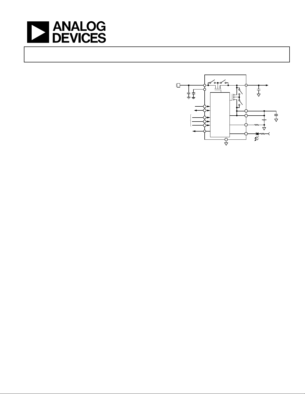
VIN
VBUS
AC OR
USB
SCL
SDA
DIG_IO1
DIG_IO2
DIG_IO3
AGND
+
Li-ion
THR
C3
47µF
C2
10nF
C1
10µF
C4
22µF
ISO_S
ISO_B
BAT_SNS
ADP5061
SYS_EN
SYSTEM
PROGRAMMABLE
ILED
VLED
CBP
CHARGER
CONTROL
BLOCK
10544-001
Data Sheet
FEATURES
2.6 mm × 2 mm WLCSP package
Fully programmable via I
Flexible digital control inputs
Up to 2.1 A current from an ac charger in LDO mode
Operating input voltage from 4.0 V to 6.7 V
Tolerant input voltage from −0.5 V to +20 V (USB VBUS)
Fully compatible with USB 3.0 and USB Battery Charging
Specification 1.2
Built-in current sensing and limiting
As low as 30 mΩ battery isolation FET between battery and
charger output
Thermal regulation prevents over heating
Compliant with JEITA 1 and JEITA 2 Li-Ion battery charging
temperature specifications
SYS_EN flag permits the system to be disabled until battery is at
minimum required level for guaranteed system start-up
2
C
TYPICAL APPLICATION CIRCUIT
Figure 1.
APPLICATIONS
Digital still cameras
Digital video cameras
Single cell Li-Ion portable equipment
PDAs, audio, and GPS devices
Portable medical devices
Mobile phones
GENERAL DESCRIPTION
The ADP5061 charger is fully compliant with USB 3.0 and the
USB Battery Charging Specification 1.2 and enables charging
via the mini USB VBUS pin from a wall charger, car charger, or
USB host port.
The ADP5061 operates from a 4 V to 6.7 V input voltage range
but is tolerant of voltages up to 20 V. The 20 V voltage tolerance
alleviates the concerns about the USB bus spiking during disconnect or connect scenarios.
The ADP5061 features an internal FET between the linear
charger output and the battery. This permits battery isolation
and, hence, system powering under a dead battery or no battery
scenario, which allows for immediate system function on connection to a USB power supply.
Based on the type of USB source, which is detected by an external
USB detection chip, the ADP5061 can be set to apply the correct
current limit for optimal charging and USB compliance.
The ADP5061 has three factory programmable digital input/output
pins that provide maximum flexibility for different systems.
These digital input/output pins permit combinations of features
such as, input current limits, charging enable and disable,
charging current limits, and a dedicated interrupt output pin.
responsibility is assumed by Analog Devices for its use, nor for any infringements of patents or other
rights of third parties that may result from its use. Specifications subject to change without notice. No
license is granted by implication or otherwise under any patent or patent rights of Analog Dev ices.
One Technology Way, P.O. Box 9106, Norwood, MA 02062-9106, U.S.A.
Tel: 781.329.4700
www.analog.com
Page 2

ADP5061 Data Sheet
TABLE OF CONTENTS
Features .............................................................................................. 1
Applications ....................................................................................... 1
Typical Application Circuit ............................................................. 1
General Description ......................................................................... 1
Revision History ............................................................................... 2
Specifications ..................................................................................... 3
Recommended Input and Output Capacitances ...................... 6
I2C-Compatible Interface Timing Specifications ..................... 6
Absolute Maximum Ratings ....................................................... 7
Thermal Resistance ...................................................................... 7
ESD Caution .................................................................................. 7
Pin Configuration and Function Descriptions ............................. 8
Typical Performance Characteristics ............................................. 9
Temperature Characteristics ..................................................... 11
Typical Waveforms ..................................................................... 13
Theory of Operation ...................................................................... 14
Summary of Operation Modes ................................................. 14
Introduction ................................................................................ 15
Charger Modes............................................................................ 17
Thermal Management ............................................................... 20
Battery Isolation FET ................................................................. 20
Battery Detection ....................................................................... 20
Battery Pack Temperature Sensing .......................................... 21
I2C Interface ................................................................................ 25
I2C Register Map ......................................................................... 26
Register Bit Descriptions ........................................................... 27
Applications Information .............................................................. 35
External Components ................................................................ 35
PCB Layout Guidelines.............................................................. 37
Power Dissipation and Thermal Considerations ....................... 38
Charger Power Dissipation ....................................................... 38
Junction Temperature ................................................................ 38
Factory Programmable Options ................................................... 39
Charger Options ......................................................................... 39
I2C Register Defaults .................................................................. 40
Digital Input and Output Options ........................................... 40
Packaging and Ordering Information ......................................... 42
Outline Dimensions ................................................................... 42
Ordering Guide .......................................................................... 42
REVISION HISTORY
6/12—Revision 0: Initial Version
Rev. 0 | Page 2 of 44
Page 3

Data Sheet ADP5061
Parameter
Symbol
Min
Typ
Max
Unit
Test Conditions/Comments
Hysteresis
50
100
150
mV
Hysteresis, higher of V
and V
rising1
VINx Current Consumption
I
2 mA
Charging or LDO mode
−65 +35
mA
I
= 1000 mA to 1300 mA
Hysteresis
ΔV
100 mV
On BAT_SNS2
Termination Voltage Accuracy
−0.25
+0.25
%
On BAT_SNS, TJ = 25°C, I
= 52.5 mA2
−1.15
+1.20
%
TJ = −40°C to +125°C
Battery Short Detection Current
I
20 mA
I
= I
Charging Soft Start Current
I
185
260
365
mA
V
> V
3.3
3.5
3.7 VTRM[5:0] programming < 4.00 V
SPECIFICATIONS
−40°C < TJ < +125°C, V
C
= 10 nF, all registers at default values, unless otherwise noted.
CBP
Table 1.
= 5.0 V, V
VIN
HOT
< V
THR
< V
COLD
, V
BAT_ SNS
= 3.6 V, V
ISO_B
= V
BAT_ SNS
, C
VIN
= 10 µF, C
= 22 µF, C
ISO_S
ISO_B
= 22 µF,
GENERAL PARAMETERS
Undervoltage Lockout V
Total Input Current I
2.25 2.35 2.5 V Falling threshold, higher of V
UVLO
VIN
74 92 100 mA Nominal USB initialized current level2
LIM
VIN
BAT_SNS
and V
BAT_SNS
1
114 150 mA USB super speed
300 mA USB enumerated current level (specification for China)
425 470 500 mA USB enumerated current level
900 mA Dedicated charger input
1500 mA Dedicated wall charger
QVIN
I
Battery Current Consumption I
5 µA Standby, includes ISO_Sx pin leakage, V
280 450 µA DIS_IC1 = high, V
QVIN_D IS
20 µA LDO mode, V
QBATT
= −40°C to +85°C
T
J
ISO_S
ISO_B
> V
< VINx < 5.5 V
BAT_SNS
= 0 V,
VIN
0.5 0.9 mA Standby, battery monitor active
CHARGER
Fast Charge Current CC Mode I
Fast Charge Current Accuracy −40 +30 mA I
−50 +30 mA I
Trickle Charge Current2 I
Weak Charge Current
2, 3
I
715 750 775 mA V
CHG
16 20 25 mA
TRK_DEAD
CHG_WEAK
I
TRK_DEAD
+ I
mA
CHG
= 3.9 V; fast charge current accuracy is
ISO_B
guaranteed at temperatures from T
J
isothermal regulation limit (typically T
= 50 mA to 550 mA
CHG
= 600 mA to 950 mA
CHG
CHG
= −40°C to
= +115°C)
J
Trickle to Weak Charge Threshold
Dead Battery V
2.4 2.5 2.6 V V
TRK_DEA D
TRK_DEAD
TRK_DEA D
< V
BAT_SNS
< V
WEAK
2, 4
Weak Battery Threshold
Weak to Fast Charge Threshold V
ΔV
Battery Termination Voltage V
2.89 3.0 3.11 V On BAT_SNS
WEAK
100 mV
WEAK
4.200 V
TRM
2, 4
END
−0.96 +0.89 % TJ = 0°C to 115°C2
2, 3
Battery Overvoltage Threshold V
Charge Complete Current I
Charging Complete Current Threshold
Accuracy
59 123 I
Recharge Voltage Differential V
Battery Node Short Threshold Voltage2 V
Charging Start Voltage Limit V
Charging Soft Start Timer t
BATTERY ISOLATION FET
Bump to Bump Resistance Between
ISO_Sx and ISO_Bx
Regulated System Voltage: V
Battery Supplementary Threshold V
Low V
BAT
VIN −
BATOV
V Relative to VINx voltage, BAT_SNS rising
0.075
15 52.5 98 mA V
END
17 83 mA I
160 260 390 mV Relative to V
RCH
2.2 2.4 2.5 V
BAT_S HR
TRK_SHORT
3.6 3.7 3.8 V Voltage limit is not active by default
CHG_VLIM
CHG_START
3 ms
CHG_START
R
30 49 mΩ On battery supplement mode, VINx = 0 V, V
DSONISO
3.6 3.8 4.0 V VTRM[5:0] programming ≥ 4.00 V
ISO_SFC
0 5 12 mV V
THISO
Rev. 0 | Page 3 of 44
= V
< V
TRM
, BAT_SNS falling2
TRM
2
TRK_DEAD
TRK_DEAD
, V
rising
ISO_B
SYS
BAT_SNS
= 52.5 mA, TJ = 0°C to 115°C2
END
= 92.5 mA, TJ = 0°C to 115°C
END
TRK_SHORT
BAT_SNS
= 500 mA
I
ISO_B
ISO_S
ISO_B
= 4.2 V,
Page 4

ADP5061 Data Sheet
VINx Transition Timing
T
10
µs
Minimum rise time for VINx from 5 V to 20 V
Thermal Early Warning Temperature
T
130 °C
110 °C
TJ falling
100,000 NTC
I
40
μA
Resistance Thresholds
Cold to Cool Resistance
R
24,400
Ω
JEITA Typical Temperature
T
°C
Normal battery charging occurs at default/programmed
Resistance Thresholds
Typical to Warm Resistance
R
4260
5200
6140 Ω
Hot to Warm Resistance
R
3700 Ω
JEITA Hot Temperature
T
60 °C
No battery charging occurs
Parameter Symbol Min Typ Max Unit Test Conditions/Comments
LDO AND HIGH VOLTAGE BLOCKING
Regulated System Voltage V
Load Regulation −0.28 %/A I
High Voltage Blocking FET (LDO FET)
On Resistance
Maximum Output Current 2.1 A V
VINx Input Voltage, Good Threshold
Rising
VINx Falling V
VINx Input Overvoltage Threshold V
Hysteresis ΔV
T
THERMAL CONTROL
Isothermal Charging Temperature T
Thermal Shutdown Temperature TSD 140 °C TJ rising
THERMISTOR CONTROL
Thermistor Current
10,000 NTC I
Thermistor Capacitance C
Cold Temperature Threshold T
Resistance Thresholds
Cool to Cold Resistance R
Cold to Cool Resistance R
Hot Temperature Threshold T
4.214 4.3 4.386 V VSYSTEM[2:0] = 000 (binary) = 4.3 V, I
ISO_STRK
LDO mode
ISO_S
R
330 485 mΩ I
DS(ON)HV
V
3.75 3.9 4.0 V
VIN_OK_RISE
3.6 3.7 V
VIN_OK_FALL
6.7 6.9 7.2 V
VIN_OV
0.1 V
VIN_OV
VIN_RISE
10 µs Minimum fall time for VINx from 4 V to 0 V
VIN_FALL
115 °C
LIM
SDL
400 μA
NTC_10k
NTC_100k
100 pF
NTC
0 °C No battery charging occurs
NTC_COLD
20,500 25,600 30,720 Ω
COLD_FA LL
24,400 Ω
COLD_R ISE
60 °C No battery charging occurs
NTC_HOT
VIN
ISO_S
2
= 0 m A to 1500 mA
= 500 mA
= 4.3 V, LDO mode
= 100 mA,
ISO_S
Hot to Typical Resistance R
Typical to Hot Resistance R
JEITA1 Li-ION BATTERY CHARGING
SPECIFICATION DEFAULTS
5
JEITA Cold Temperature T
3700 Ω
HOT_FALL
HOT_RIS E
2750 3350 3950 Ω
0 °C No battery charging occurs
JEITA_C OLD
Resistance Thresholds
Cool to Cold Resistance R
JEITA Cool Temperature T
20,500 25,600 30,720 Ω
COLD_FA LL
COLD_R ISE
10 °C Battery charging occurs at 50% of programmed level
JEITA_ COOL
Resistance Thresholds
Typical to Cool Resistance R
Cool to Typical Resistance R
Warm to Typical Resistance R
JEITA Warm Temperature T
13,200 16,500 19,800 Ω
TYP_FALL
15,900 Ω
TYP_RISE
JEITA_TY P
5800 Ω
WARM_FALL
WARM_RISE
45 °C Battery termination voltage (V
JEITA_WARM
Resistance Thresholds
HOT_FALL
Warm to Hot Resistance R
HOT_RIS E
JEITA_H OT
2750 3350 3950 Ω
levels
) is reduced by 100 mV
TRM
Rev. 0 | Page 4 of 44
Page 5

Data Sheet ADP5061
JEITA Cool Temperature
T
10 °C
Battery termination voltage (V
) is reduced by 100 mV
JEITA Warm Temperature
T
45 °C
Battery termination voltage (V
) is reduced by 100 mV
Battery Detection
High
V
3.4 V
Battery Detection Timer
t
333 ms
Fast Charge
t
600 min
Deglitch
tDG 31 ms
Applies to V
, V
, I
, V
, V
Battery Short2
t
30 sec
ILED OUTPUT PINS
Maximum Voltage on Digital Inputs
V
5.5 V Applies to SCL, SDA, DIG_IO1, DIG_IO2, DIG_IO3
Minimum Logic High Input Voltage
VIH
1.2 V Applies to SCL, SDA, DIG_IO1, DIG_IO2, DIG_IO3
Parameter Symbol Min Typ Max Unit Test Conditions/Comments
JEITA2 Li-ION BATTERY CHARGING
SPECIFICATION DEFAULTS
5
JEITA Cold Temperature T
Resistance Thresholds
Cool to Cold Resistance R
Cold to Cool Resistance R
Resistance Thresholds
Typical to Cool Resistance R
Cool to Typical Resistance R
JEITA Typical Temperature T
Resistance Thresholds
Warm to Typical Resistance R
Typical to Warm Resistance R
Resistance Thresholds
Hot to Warm Resistance R
Warm to Hot Resistance R
JEITA Hot Temperature T
BATTERY DETECTION
0 °C No battery charging occurs
JEITA_C OLD
20,500 25,600 30,720 Ω
COLD_FA LL
24,400 Ω
COLD_R ISE
JEITA_ COOL
13,200 16,500 19,800 Ω
TYP_FALL
15,900 Ω
TYP_RISE
°C Normal battery charging occurs at
JEITA_TY P
default/programmed levels
5800 Ω
WARM_FALL
WARM_RISE
JEITA_WARM
HOT_FALL
HOT_RIS E
JEITA_H OT
4260 5200 6140 Ω
3700 Ω
2750 3350 3950 Ω
60 °C No battery charging occurs
TRM
TRM
Sink Current I
Source Current I
13 20 34 mA
SINK
7 10 13 mA
SOUR CE
Battery Threshold
Low V
1.8 1.9 2.0 V
BATL
BATH
BATOK
TIMERS
Clock Oscillator Frequency f
Start Charging Delay t
Trickle Charge t
Charge Complete t
Watchdog2 tWD 32 sec
Safety t
Voltage Drop over ILED V
Maximum Operating Voltage over
2.7 3 3.3 MHz
CLK
1 sec
START
60 min
TRK
CHG
7.5 min V
END
36 40 44 min
SAFE
BAT_S HR
200 mV I
ILED
V
5.5 V
MAXILED
BAT_SNS
= 20 mA
ILED
= V
TRM
, I
< I
CHG
END
TRK
RCH
END
DEAD
VIN_OK
ILED
SYS_EN OUTPUT PIN
SYS_EN FET On Resistance R
10 Ω I
ON_SYS_EN
SYS_EN
= 20 mA
LOGIC INPUT PIN
DIN_MAX
Maximum Logic Low Input Voltage VIL 0.5 V Applies to SCL, SDA, DIG_IO1, DIG_IO2, DIG_IO3
Pull-Down Resistance 215 350 610 kΩ Applies to DIG_IO1, DIG_IO2, DIG_IO3
1
Undervoltage lockout generated normally from ISO_Sx or ISO_Bx; in certain transition cases, it can be generated from VINx.
2
These values are programmable via I2C. Values are given with default register values.
3
The output current during charging may be limited by the input current limit or by the isothermal charging mode.
4
During weak charging mode, the charger provides at least 20 mA of charging current via the trickle charge branch to the battery unless trickle charging is disabled.
Any residual current, which is not required by the system, is also used to charge the battery.
5
Either JEITA1 (default) or JEITA2 can be selected in I2C, or both JEITA functions can enabled or disabled in I2C.
Rev. 0 | Page 5 of 44
Page 6
ADP5061 Data Sheet
CAPACITANCES
Hold Time for Start/Repeated Start
t
0.6
µs
Pulse Width of Suppressed Spike
tSP 0
50
ns
SD
RECOMMENDED INPUT AND OUTPUT CAPACITANCES
Table 2.
Parameter Symbol Min Typ Max Unit Test Conditions/Comments
VINx C
CBP C
ISO_Sx C
ISO_Bx C
4 10 μF Effective capacitance
VIN
BP
20 47 100 μF Effective capacitance
ISO_S
10 22 μF Effective capacitance
ISO_B
6 10 14 nF Effective capacitance
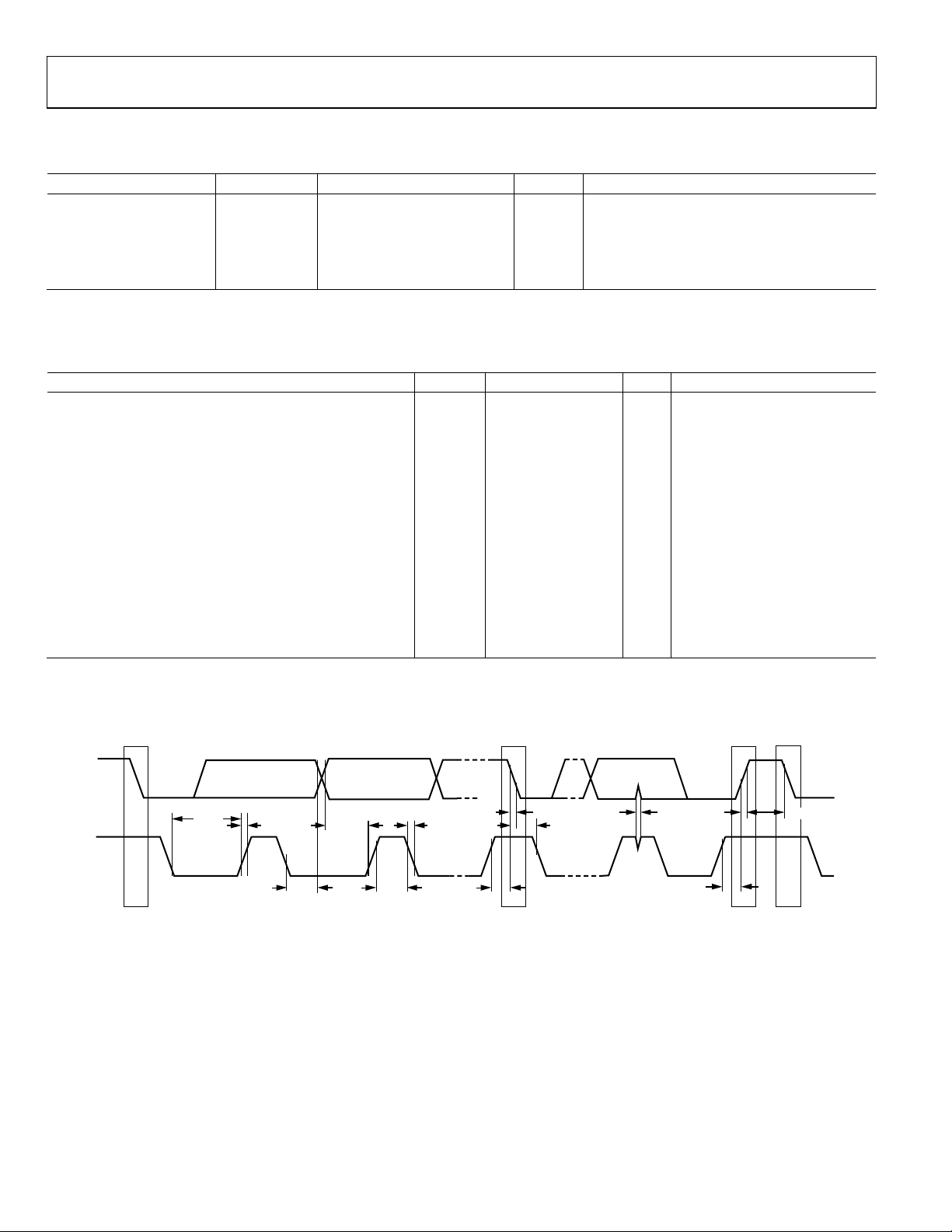
I2C-COMPATIBLE INTERFACE TIMING SPECIFICATIONS
Table 3.
Parameter1 Symbol Min Typ Max Unit Test Conditions/Comments
I2C-COMPATIBLE INTERFACE2
Capacitive Load for Each Bus Line CS 400 pF
SCL Clock Frequency f
SCL High Time t
SCL Low Time t
Data Setup Time t
Data Hold Time t
Setup Time for Repeated Start t
Bus Free Time Between a Stop and a Start Condition t
Setup Time for Stop Condition t
Rise Time of SCL/SDA tR 20 300 ns
Fall Time of SCL/SDA tF 20
1
Guaranteed by design.
2
A master device must provide a hold time of at least 300 ns for the SDA signal to bridge the undefined region of the falling edge of SCL (see Figure 2).
Timing Diagram
400 kHz
SCL
0.6 µs
HIGH
1.3 µs
LOW
100 ns
SU, DAT
0 0.9 µs
HD, DAT
0.6 µs
SU, STA
HD, STA
1.3 µs
BUF
0.6 µs
SU, STO
300 ns
A
SCL
S Sr P S
S = START CONDITION
Sr = REPEATED START CONDITION
P = STOP CONDITION
t
LOW
t
HD, DAT
t
SU, DAT
t
t
HIGH
Figure 2. I
Rev. 0 | Page 6 of 44
F
t
2
C Timing Diagram
t
R
t
BU, STA
F
t
HD, STA
t
SP
t
BU, STO
t
R
t
BUF
10544-002
Page 7
Data Sheet ADP5061
VIN1, VIN2, VIN3 to AGND
–0.5 V to +20 V
Stresses a bove those l isted under Absolute Maximum Ratings
may cause permanent damage to the device. This is a stress
rating only; functional operation of the device at these or any
other conditions above those indicated in the operational
section of this specification is not implied. Exposure to absolute
maximum rating conditions fo r extended periods may affect
device reliability.
ABSOLUTE MAXIMUM RATINGS
Table 4. Absolute Maximum Ratings
Parameter Rating
All Other Pins to AGND –0.3 V to +6 V
Continuous Drain Current, Battery Supple-
mentary Mode, from ISO_Bx to ISO_Sx
Storage Temperature Range –65°C to +150°C
Operating Junction Temperature Range –40°C to +125°C
Soldering Conditions JEDEC J-STD-020
2.1 A
THERMAL RESISTANCE
θJA is specified for the worst-case conditions, that is, θJA is
specified for a device soldered in a circuit board for surfacemount packages.
Table 5. Thermal Resistance
Package Type θJA θJC θJB Unit
20-Lead WLC SP1 46.8 0.7 9.2 °C/W
1
5 × 4 array, 0.5 mm pitch (2.6 mm × 2.0 mm); based on a JEDEC 2S2P, 4-layer
board with 0 m/sec airflow.
Maximum Power Dissipation
The maximum safe power dissipation in the ADP5061 package
is limited by the associated rise in junction temperature (T
the die. At a die temperature of approximately 150°C (the glass
transition temperature), the properties of the plastic change.
Even temporarily exceeding this temperature limit may change
the stresses that the package exerts on the die, thereby permanently shifting the parametric performance of the ADP5061.
Exceeding a junction temperature of 175°C for an extended
period can result in changes in the silicon devices, potentially
causing failure.
) on
J
ESD CAUTION
Rev. 0 | Page 7 of 44
Page 8
ADP5061 Data Sheet
TOP VIEW
(BALL SI DE DOWN)
Not to Scale
1
A
B
C
D
E
2 3 4
BALL A1 CORNER
ILED
AGND
ISO_B3
ISO_B2
SDA
CBP
VIN3
VIN2
SCL
DIG_IO3
DIG_IO2
BAT_SNS
SYS_EN
THR
ISO_S3
ISO_S2
ISO_B1 VIN1 DIG_IO1ISO_S1
10544-003
PIN CONFIGURATION AND FUNCTION DESCRIPTIONS
Figure 3. Pin Configuration
Table 6. Pin Function Descriptions
Pin No. Name Type1 Description
E2, D2, C2 ISO_S1, ISO_S2,
ISO_S3
I/O Linear Charger Supply Side Input to the Internal Isolation FET/Battery Current Regulation FET.
High current input/output.
E3, D3, C3 VIN1, VIN2, VIN3 I/O Power Connections to USB VBUS. These pins are high current inputs when in charging mode.
B1 AGND G Analog Ground.
E1, D1, C1 ISO_B1, ISO_B2,
I/O Battery Supply Side Input to Internal Isolation FET/Battery Current Regulation FET.
ISO_B3
A4 SCL I I2C-Compatible Interface Serial Clock.
A3 SDA I/O I2C-Compatible Interface Serial Data.
E4 DIG_IO1 GPIO Set Input Current Limit. This pin sets the input current limit directly. When DIG_IO1 = low or
high-Z, the input limit is 100 mA. When DIG_IO1 = high, the input limit is 500 mA.
2, 3
C4 DIG_IO2 GPIO Disable IC1. This pin sets the charger to the low current mode. When DIG_IO2 = low or high-Z, the
charger operates in normal mode. When DIG_IO2 = high, the LDO and the charger are disabled
and VINx current consumption is 280 µA (typical). 20 V VINx input protection is disabled and VINx
B4 DIG_IO3 GPIO Enable Charging. When DIG_IO3 = low or high-Z, charging is disabled. When DIG_IO3 = high,
B2 THR I Battery Pack Thermistor Connection. If this pin is not used, connect a dummy 10 kΩ resistor from THR
voltage level must be equal to or lower than 5.5 V.
charging is enabled.
2, 3
to GND.
2, 3
D4 BAT _ SNS I Battery Voltage Sense Pin.
A1 ILED O Open-Drain Output to Indicator LED.
A2 SYS_EN O System Enable. This is the battery OK flag/open-drain pull-down FET pin to enable the system
B3 CBP I/O Bypass Capacitor Input.
1
I is input, O is output, I/O is input/output, G is ground, and GPIO is factory programmable general-purpose input/output.
2
See the Digital Input and Output Options section for details.
3
DIG_IOx setting defines the initial state of the ADP5061. When the parameter or the mode that is related to each DIG_IOx pin setting is changed (by programming the
equivalent I
when the battery level reaches the V
2
C register bit or bits), the I2C register setting dominates over the DIG_IOx pin setting. VINx connection or disconnection resets control to the DIG_IOx pin.
Rev. 0 | Page 8 of 44
WEAK
level.
Page 9
Data Sheet ADP5061
4.35
SYSTEM VOLTAGE (V)
4.5
4.0 4.4 4.8 5.2 5.6 6.0 6.4 6.8
SYSTEM VOLTAGE (V)
INPUT VOLTAGE (V)
LOAD = 100mA
LOAD = 500mA
LOAD = 1000mA
10544-005
0
100
200
300
400
500
600
700
800
900
1000
2.7 3.2 3.7 4.2
CHARGE CURRENT (mA)
BATTERY VOLTAGE (V)
LIMIT = 900mA
LIMIT = 500mA
LIMIT = 100mA
10544-006
4.95
4.96
4.97
4.98
4.99
5.00
5.01
5.02
5.03
5.04
5.05
0.01 0.1 1
SYSTEM VOLTAGE (V)
SYSTEM OUTPUT CURRENT ( A)
10544-007
5.4
4.0 4.4 4.8 5.2 5.6 6.0 6.4 6.8
SYSTEM VOLTAGE (V)
INPUT VOLTAGE (V)
LOAD = 100mA
LOAD = 500mA
LOAD = 1000mA
10544-008
0
100
200
300
400
500
600
700
2.3 2.8 3.3 3.8 4.3
CHARGE CURRENT (mA)
BATTERY VOLTAGE (V)
WEAK
CHARGE
FAST CHARGE
TRICKLE CHARGE
10544-009
TYPICAL PERFORMANCE CHARACTERISTICS
V
= 5.0 V, C
VIN
4.34
4.33
4.32
4.31
4.30
4.29
4.28
4.27
4.26
4.25
0.01 0.1 1
Figure 4. System Voltage vs. System Output Current, LDO Mode,
= 10 µF, C
VIN
SYSTEM OUTPUT CURRENT ( A)
= 44 µF, C
ISO_S
VSYSTEM[2:0] = 000 (Binary) = 4.3 V
= 22 µF, CBP = 10 nF, all registers at default values, unless otherwise noted.
ISO_B
10544-004
Figure 7. System Voltage vs. System Output Current, LDO Mode, V
VSYSTEM[2:0] = 111 (Binary) = 5.0 V
= 6.0 V,
VIN
4.4
4.3
4.2
4.1
4.0
3.9
3.8
3.7
3.6
3.5
Figure 5. Output Voltage vs. Input Voltage (In Dropout), LDO Mode,
VSYSTEM[2:0] = 000 (Binary) = 4.3 V
Figure 6. Input Current-Limited Charge Current vs. Battery Voltage
5.2
5.0
4.8
4.6
4.4
4.2
4.0
3.8
3.6
3.4
Figure 8. Output Voltage vs. Input Voltage (In Dropout), LDO Mode,
VSYSTEM[2:0] = 111 (Binary) = 5.0 V
Figure 9. Battery Charge Current vs. Battery Voltage, ICHG[4:0] = 01001
(Binary) = 500 mA, ILIM[3:0] = 1111 (Binary) = 2100 mA
Rev. 0 | Page 9 of 44
Page 10
ADP5061 Data Sheet
20
22
24
26
28
30
32
34
36
38
40
2.7 3.2 3.7 4.2
ISOLATION FET RESISTANCE (mΩ)
BATTERY VOLTAGE (V)
10544-010
0
0.5
1.0
1.5
2.0
2.5
3.0
3.5
4.0
0 2 4 6 8
VINx CURRENT (mA)
INPUT VOLTAGE (V)
DEFAULT STARTUP
DIS_LDO = HIGH
DIS_IC1 = HIGH
10544-011
20
22
24
26
28
30
32
34
36
38
40
0 0.5 1.0 1.5 2.0
ISOLATION FET RESISTANCE (mΩ)
LOAD CURRENT ( A)
10544-012
0
0.1
0.2
0.3
0.4
0.5
0.6
0.7
3.0
3.2
3.4
3.6
3.8
4.0
4.2
4.4
0 50 100 150
CHARGE CURRENT (A)
BATTERY VOLTAGE (A)
CHARGE TIM E ( min)
V
BAT_SNS
I
ISO_B
10544-013
Figure 10. Ideal Diode RON vs. Battery Voltage, I
Figure 11. VINx Current vs. VINx Voltage
= 500 mA, VINx Open
ISO_S
Figure 12. Ideal Diode RON vs. Load Current, V
ISO_B
= 3.6 V
Figure 13. Charge Profile, ILIM[3:0] = 0110 (Binary) = 500 mA, Battery
Capacity = 925 mAh
Rev. 0 | Page 10 of 44
Page 11
Data Sheet ADP5061
0
0.1
0.2
0.3
0.4
0.5
0.6
0.7
0.8
0.9
1.0
1.1
1.2
1.3
1.4
1.5
–40 –15 10 35 60 85
STANDBY CURRENT (µA)
AMBIENT TEMPERATURE (°C)
V
ISO_B
= 3.6V
V
ISO_B
= 4.2V
V
ISO_B
= 5.5V
10544-014
0
0.05
0.10
0.15
0.20
0.25
0.30
0.35
0.40
0.45
0.50
–40 –25 –10 5 20 35 50 65 80 95 110 125
VINx QUIE S CE NT CURRENT (mA)
AMBIENT TEMPERATURE (°C)
V
IN
= 4.0V
V
IN
= 5.0V
V
IN
= 5.5V
10544-015
–0.5
–0.4
–0.3
–0.2
–0.1
0
0.1
0.2
0.3
0.4
0.5
–40 –25 –10 5 20 35 50 65 80 95 110 125
SYSTEM VOLTAGE ACCURACY (%)
AMBIENT TEMPERATURE (°C)
V
ISO_S
= 4.3V
V
ISO_S
= 5.0V
10544-016
–0.5
–0.4
–0.3
–0.2
–0.1
0
0.1
0.2
0.3
0.4
0.5
–40 –25 –10 5 20 35 50 65 80 95 110 125
SYSTEM VOLTAGE ACCURACY (%)
AMBIENT TEMPERATURE (°C)
V
ISO_S
= 4.3V
V
ISO_S
= 5.0V
10544-017
0
0.5
1.0
1.5
2.0
2.5
3.0
3.5
4.0
4.5
5.0
–40 –25 –10 5 20 35 50 65 80 95 110 125
VINx QUIE S CE NT CURRENT (mA)
AMBIENT TEMPERATURE (°C)
VIN = 4.0V
V
IN
= 5.0V
VIN = 6.7V
10544-018
–0.5
–0.4
–0.3
–0.2
–0.1
0
0.1
0.2
0.3
0.4
0.5
–40 –25 –10 5 20 35 50 65 80 95 110 125
VTRM VOLTAGE ACCURACY (%)
AMBIENT TEMPERATURE (°C)
V
TRM
= 3.8V
V
TRM
= 4.2V
V
TRM
= 4.5V
10544-019
TEMPERATURE CHARACTERISTICS
Figure 14. Battery Leakage Current vs. Ambient Temperature
Figure 15. VINx Quiescent Current vs. Ambient Temperature, DIS_IC1 = High
Figure 17. System Voltage vs. Temperature, Trickle Charge Mode,
V
= 4.3 V and VINx = 5.0 V, or V
ISO_S
= 5.0 V and VINx = 6.0 V
ISO_S
Figure 18. VINx Quiescent Current vs. Ambient Temperature, LDO Mode
Figure 16. LDO Mode Voltage vs. Ambient Temperature,
Load = 100 mA, V
= 5.5 V
VIN
Figure 19. Termination Voltage vs. Ambient Temperature
Rev. 0 | Page 11 of 44
Page 12
ADP5061 Data Sheet
1.4
–40 –15 10 35
60 85 110
CHARGE CURRENT (A)
AMBIENT TEMPERATURE (°C)
I
CHG
= 750mA
I
CHG
= 500mA
I
CHG
= 1300mA
10544-020
AMBIENT TEMPERATURE (°C)
6.80
6.85
6.90
6.95
7.00
–40 –25 –10 5 20 35 50 65 80 95 110 125
VIN OVERVOLTAGE THRESHOL D ( V )
10544-021
1.6
–40 –25 –10 5 20 35 50 65 80 95 110 125
INPUT CURRENT LIMIT ( A)
AMBIENT TEMPERATURE (°C)
I
LIM
= 1500mA
I
LIM
= 900mA
I
LIM
= 500mA
I
LIM
= 100mA
10544-022
1.3
1.2
1.1
1.0
0.9
0.8
0.7
0.6
0.5
0.4
Figure 20. Fast Charge CC Mode Current vs. Ambient Temperature
1.5
1.4
1.3
1.2
1.1
1.0
0.9
0.8
0.7
0.6
0.5
0.4
0.3
0.2
0.1
0
Figure 22. Input Current Limit vs. Ambient Temperature
Figure 21. VINx Overvoltage Threshold vs. Ambient Temperature
Rev. 0 | Page 12 of 44
Page 13
Data Sheet ADP5061
I
VIN
I
ISO_B
V
VIN
V
ISO_S
10544-023
I
ISO_S
V
ISO_S
10544-024
I
ISO_B
V
ISO_S
V
VIN
I
VIN
10544-025
I
VIN
I
ISO_B
V
VIN
V
ISO_S
10544-026
I
ISO_S
I
ISO_B
V
ISO_S
10544-027
I
ISO_B
V
ISO_B
10544-028
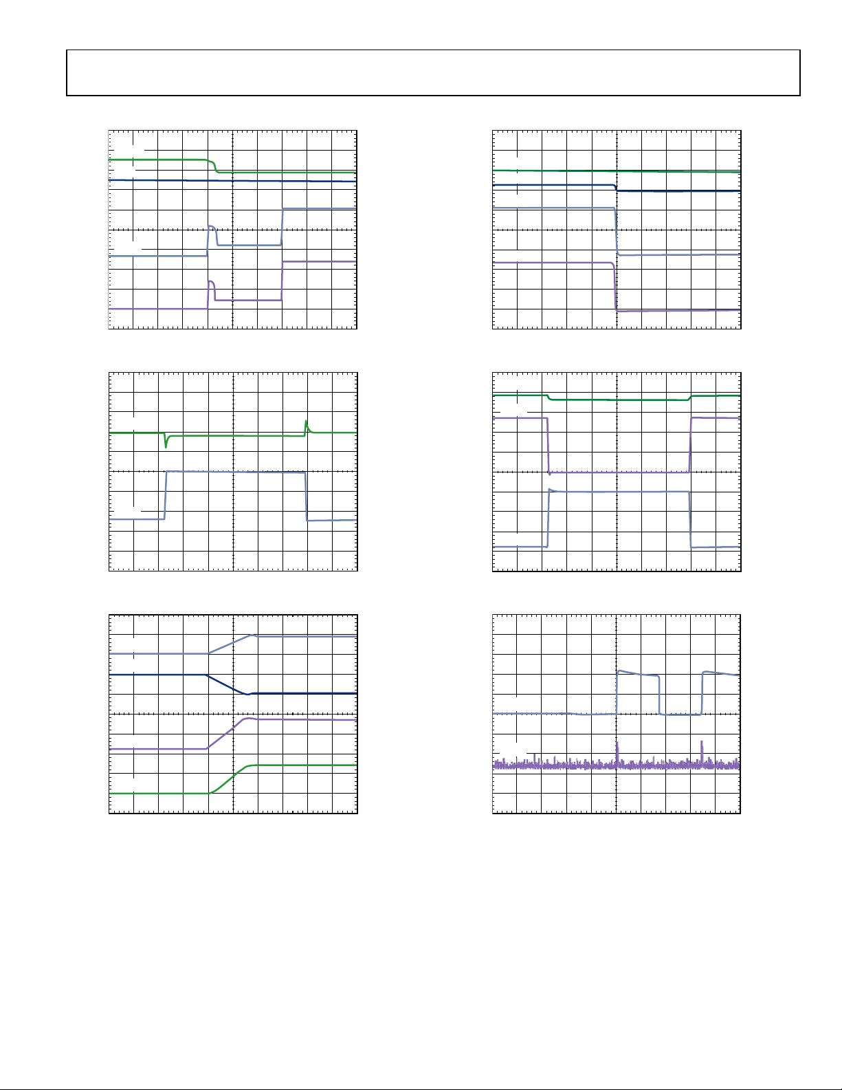
TYPICAL WAVEFORMS
Figure 23. Charging Startup, V
ICHG[4:0] = 01110 (Binary) = 750 mA
Figure 24. Load Transient, I
= 5.0 V, ILIM[3:0] = 0110 (Binary) = 500 mA,
VIN
Load = 300 mA to 1500 mA to 300 mA
ISO_Sx
Figure 26. VBUS Disconnect
Figure 27. Load Transient. I
Load = 300 mA to 1500 mA to 300 mA,
ISO_Sx
EN_CHG = High, ILIM[3:0] = 0110 (Binary) = 500 mA
Figure 25. Input Current-Limit Transition from 100 mA to 900 mA,
ISO_Sx Load = 66 Ω, Charging = 750 mA
Figure 28. Battery Detection Waveform, VSYSTEM[2:0] = 000 (Binary) = 4.3 V,
No Battery
Rev. 0 | Page 13 of 44
Page 14

ADP5061 Data Sheet
High = all charging modes enabled (fast, weak, trickle).
Yes
CHG
CHG
THEORY OF OPERATION
SUMMARY OF OPERATION MODES
Table 7. Summary of the ADP5061 Operation Modes
LDO
Mode Name
VINx
Condition
Battery Condition
Trickle
Charge
FET
State
IC Off, Standby 0 V Any battery condition Off Off On/Off Battery voltage
IC Off, Suspend 5 V Any battery condition Off Off On Battery voltage Disable IC1
LDO Mode Off, Isolation
5 V Any battery condition Off Off On Battery voltage Disable LDO and
FET On
LDO Mode Off, Isolation
5 V Any battery condition Off Off Off 0 V Enable battery
FET Off (System Off)
LDO Mode, Charger Off 5 V Any battery condition Off LDO Off 5.0 V Enable battery
Trickle Charge Mode 5 V Battery < V
Weak Charge Mode 5 V V
TRK_DEA D
≤ battery < V
Fast Charge Mode 5 V Battery ≥ V
On LDO Off 5.0 V Enable battery
TRK_DEAD
On CHG CHG 3.8 V Enable battery
WEAK
Off CHG CHG 3.8 V (min) Enable battery
WEAK
Charge Mode, No Battery 5 V Open Off LDO Off 5.0 V Enable battery
Charge Mode, Battery
5 V Short On LDO Off 5.0 V Enable battery
(ISO_Bx) Short
1
See Table 8 for details.
Battery
Isolation
FET
System
Voltage
ISO_Sx
or 0 V
Additional
Conditions
1
Disable IC1
enable isolation FET
charging
charging
charging
charging
charging
charging
charging
Table 8. Operation Mode Controls
2
C
Pin Configuration DIG_IOx
Equivalent I
Address, Data Description
Enable Battery Charging DIG_IO3 0x07, D0 Low = all charging modes disabled (fast, weak, trickle).
Disable IC1 DIG_IO2 0x07, D6
Disable IC1
1
VINx
Supply
Connected
LDO_FET ISO_FET
Low No Off On
High No Off On
Yes Off On
Disable LDO and Enable Isolation FET 0x07, D3, D0 Low = LDO enabled.
High = LDO disabled. In addition, when EN_CHG = low, the
battery isolation FET is on; when EN_CHG = high, the battery
isolation FET is off.
1
When disable IC1 mode is active and the VINx supply is connected, the supply voltage level must fulfill the following condition: V
< VIN < 5.5 V.
ISO_B
Rev. 0 | Page 14 of 44
Page 15

Data Sheet ADP5061
INTRODUCTION
The ADP5061 is a fully programmable I2C charger for single
cell lithium-ion or lithium-polymer batteries suitable for a wide
range of portable applications.
The linear charger architecture enables up to 2.1 A output
current at 4.3 V to 5.0 V (I
power supply, and up to 1.3 A charge current into the battery
from a dedicated charger.
The ADP5061 operates from an input voltage of 4 V up to 6.7 V
but is tolerant of voltages of up to 20 V. The 20 V voltage tolerance
alleviates the concerns of the USB bus spiking during disconnection or connection scenarios.
The ADP5061 features an internal FET between the linear charger
output and the battery. This feature permits battery isolation
and, hence, system powering under a dead battery or no battery
scenario, which allows for immediate system function upon
connection to a USB power supply.
The ADP5061 is fully compliant with USB 3.0 and the USB
Battery Charging Specification 1.2. The ADP5061 is chargeable
via the mini USB VBUS pin from a wall charger, car charger, or
USB host port. Based on the type of USB source, which is detected
2
C programmable) on the system
by an external USB detection device, the ADP5061 can be set to
apply the correct current limit for optimal charging and USB
compliance. The USB charger permits correct operation under
all USB-compliant sources such as wall chargers, host chargers,
hub chargers, and standard host and hubs.
A processor can control the USB charger using the I
2
C to
program the charging current and numerous other parameters,
including
• Trickle charge current level
• Trickle charge voltage threshold
• Weak charge (constant current) current level
• Fast charge (constant current) current level
• Fast charge (constant voltage) voltage level at 1% accuracy
• Fast charge safety timer period
• Watchdog safety timer parameters
• Weak battery threshold detection
• Charge complete threshold
• Recharge threshold
• Charge enable/disable
• Battery pack temperature detection and automatic charger
shutdown
Rev. 0 | Page 15 of 44
Page 16

ADP5061 Data Sheet
E3
D3
D3
E3
ISO_S1
ISO_S2
ISO_S3
VIN1
VIN2
C3
C1
ISO_B2
B2
THR
+
–
0.5V
NTC CURRENT
CONTROL
COLD
COOL
WARM
HOT
NTC
TRICKLE
CURRENT
SOURCE
B3
BATTERY
DETECTION
SINK
D4
BAT_SNS
BATTERY DETECTION
BATTERY:
OPEN
SHORT
TRICKLE
WEAK
CV-MODE
RECHARGE
CHARGE CONTROL
EOC
TO SYSTEM
LOAD
+
–
6.85V
3.9V
+
–
+
–
+
–
+
–
+
–
+
–
+
–
+
–
VIN
OVERVOLTAGE
VIN LIMIT
BATTERY
ISOLATION FET
VIN GOOD
BATTERY OVERVOLTAGE
A4
A3
SCL
SDA
TO USB VBUS
OR WALL
ADAPTER
B1
AGND
E4
C4
B4
DIG_IO1
DIG_IO2
DIG_IO3
A2
SYS_EN
3MHz OSC
SINGLE
CELL
Li-Ion
TSD 140°C
SYS_EN OUTPUT
LOGIC
THERMAL CO NTROL
C3
VIN3
CBP
ISO_B3
D1
E1
A1
ILED
ILED OUTPUT
LOGIC
HIGH VOLTAGE
BLOCKING
LDO-FET
+
–
LDO-FET
CONTROL
3.4V
I
2
C INTERFACE
AND
CONTROL LOGIC
VIN – 150mV
ISO_B1
1.9V
WARNING 130° C
ISOTHE RM AL 115°C
TSD DOWN 110°C
10544-029
Figure 29. Block Diagram
Rev. 0 | Page 16 of 44
Page 17

Data Sheet ADP5061
The ADP5061 includes a number of significant features to
optimize charging and functionality including
Thermal regulation for maximum performance
USB host current-limit accuracy: ±5%.
Termination voltage accuracy: ±1%.
Battery thermistor input with automatic charger shutdown
in the event that the battery temperature exceeds limits
(compliant with the JEITA Li-Ion battery charging
temperature specification).
Three external pins (DIG_IO1, DIG_IO2, and DIG_IO3)
that directly control a number of parameters. These pins
are factory programmable for maximum flexibility. They
can be factory programmed for functions such as
Enable/disable charging.
Control of 100 mA or 500 mA input current limit.
Control of 1500 mA input current limit.
Control of the battery charge current.
Interrupt output pin.
See the Digital Input and Output Options section for details.
CHARGER MODES
Input Current Limit
The VINx input current limit is controlled via the internal I2C
ILIM bits. The input current limit can also be controlled via the
DIG_IO1 pin (if factory programmed to do so) as outlined in
Table 9. Any change in the I
over the pin setting.
2
C default from 100 mA dominates
Table 9. DIG_IO1 Operation
DIG_IO1 Function
0
100 mA input current limit or I
2
C programmed
value
1
500 mA input current limit or I
value (or reprogrammed I
2
C programmed
2
C value from 100 mA
default)
USB Compatibility
The ADP5061 features an I2C programmable input current limit
to ensure compatibility with the requirements listed in Table 10.
The current limit defaults to 100 mA to allow compatibility
with a USB host or hub that is not configured.
2
The I
C register default is 100 mA. An I2C write command to
the ILIM bits override the DIG_IOx pins, and the I
2
C register
default value can be reprogrammed for alternative
requirements.
When the input current-limit feature is used, the available input
current may be too low for the charger to meet the programmed
charging current, I
, thereby reducing the rate of charge and
CHG
setting the VIN_ILIM flag.
When connecting voltage to VINx without the proper voltage
level on the battery side, the high voltage blocking mechanism
is in a state wherein it draws only the current of <1 mA until
V
reaches the VIN_OK level.
IN
The ADP5061 charger provides support for the following connections through the single connector VINx pin (see Table 10).
Table 10. Input Current Compatibility with Standard USB Limits
Mode Standard USB Limit ADP5061 Func tion
USB (China Only) 100 mA limit for standard USB host or hub 100 mA input current limit or I2C programmed value
300 mA limit for Chinese USB specification 300 mA input current limit or I2C programmed value
USB 2.0 100 mA limit for standard USB host or hub 100 mA input current limit or I2C programmed value
500 mA limit for standard USB host or hub 500 mA input current limit or I2C programmed value
USB 3.0 150 mA limit for superspeed USB 3.0 host or hub 150 mA input current limit or I2C programmed value
900 mA limit for superspeed, high speed USB host or hub
900 mA input current limit or I
2
C programmed value
charger
Dedicated Charger
1500 mA limit for dedicated charger or low/full speed USB
1500 mA input current limit or I
2
C programmed value
host or hub charger
Rev. 0 | Page 17 of 44
Page 18

ADP5061 Data Sheet
Trickle Charge Mode
A deeply discharged Li-Ion cell can exhibit a very low cell
voltage, making it unsafe to charge the cell at high current rates.
The ADP5061 charger uses a trickle charge mode to reset the
battery pack protection circuit and lift the cell voltage to a safe
level for fast charging. A cell with a voltage below V
charged with the trickle mode current, I
TRK_DEAD
. During trickle
TRK_DEAD
is
charging mode, the CHARGER_STATUS bits are set.
During trickle charging, the ISO_Sx node is regulated to
V
by the LDO and the battery isolation FET is off, which
ISO_STRK
means that the battery is isolated from the system power supply.
Trickle Charge Mode Timer
The duration of trickle charge mode is monitored to ensure that
the battery is revived from its deeply discharged state. If trickle
charge mode runs for longer than 60 minutes without the cell
voltage reaching V
, a fault condition is assumed and
TRK_DEAD
charging stops. The fault condition is asserted on the
CHARGER_STATUS bits, allowing the user to initiate the fault
recovery procedure specified in the Fault Recovery section.
Weak Charge Mode (Constant Current)
When the battery voltage exceeds V
V
, the charger switches to intermediate charge mode.
WEAK
but is less than
TRK_DEAD
During the weak charge mode, the battery voltage is too low to
allow the full system to power-up. Because of the low battery
level, the USB transceiver cannot be powered and, therefore,
cannot enumerate for more current from a USB host. Consequently, the USB limit remains at 100 mA.
The system microcontroller may or may not be powered by the
charger output voltage (V
), depending upon the amount
ISO_SFC
of current required by the microcontroller and/or the system
architecture. When the ISO_Sx pins power the microcontroller,
the battery charge current (I
CHG_W EAK
) cannot be increased above
20 mA to ensure the microcontroller operation (if doing so),
nor can I
CHG_W EAK
be increased above the 100 mA USB limit.
Thus, set the battery charging current as follows:
• Set the default 20 mA via the linear trickle charger branch (to
ensure that the microprocessor remains alive if powered by
the main charger output, ISO_Sx). Any residual current on
the main charger output, ISO_Sx, is used to charge the
bat t e r y.
• During weak current mode, other features may prevent the
weak charging current from reaching its full programmed
value. Isothermal charging mode or input current limiting
for USB compatibility can affect the programmed weak
charging current value under certain operating conditions.
During weak charging, the ISO_Sx node is regulated to
V
by the battery isolation FET.
ISO_SFC
Fast Charge Mode (Constant Current)
When the battery voltage exceeds V
TRK_DEAD
and V
WEAK
, the
charger switches to fast charge mode, charging the battery with
the constant current, I
. During fast charge mode (constant
CHG
current), the CHARGER_STATUS bits are set to 010.
During constant current mode, other features may prevent the
current, I
, from reaching its full programmed value.
CHG
Isothermal charging mode or input current limiting for USB
compatibility can affect the value of I
under certain oper-
CHG
ating conditions. The voltage on ISO_Sx is regulated to stay at
V
by the battery isolation FET when V
ISO_SFC
ISO_B
< V
ISO_SFC
.
Fast Charge Mode (Constant Voltage)
As the battery charges, its voltage rises and approaches the termination voltage, V
. The ADP5061 charger monitors the voltage
TRM
on the BAT_SNS pin to determine when charging should end.
Howeve r, the internal ESR of the battery pack, combined with
the printed circuit board (PCB) and other parasitic series
resistances creates a voltage drop between the sense point at the
BAT_SNS pin and the cell terminal. To compensate for this and
ensure a fully charged cell, the ADP5061 enters a constant voltage
charging mode when the termination voltage is detected on the
BAT_SNS pin. The ADP5061 reduces charge current gradually as
the cell continues to charge, maintaining a voltage of V
TRM
on the
BAT_SNS pin. During fast charge mode (constant voltage), the
CHARGER_ STATUS register is set.
Fast Charge Mode Timer
The duration of fast charge mode is monitored to ensure that
the battery is charging correctly. If the fast charge mode runs for
longer than t
reaching V
without the voltage at the BAT_SNS pin
CHG
, a fault condition is assumed and charging stops.
TRM
The fault condition is asserted on the CHARGER_STATUS bits
allowing the user to initiate the fault recovery procedure as
specified in the Fault Recovery section.
If the fast charge mode runs for longer than t
CHG
, and V
TRM
has
been reached on the BAT_SNS pin but the charge current has
not yet fallen below I
, charging stops. No fault condition is
END
asserted in this circumstance and charging resumes as normal if
the recharge threshold is breached.
Watchdog Timer
The ADP5061 charger features a programmable watchdog timer
function to ensure charging is under the control of the processor.
The watchdog timer starts running when the
ADP5061 cha
rger
determines that the processor should be operational, that is,
when the processor sets the RESET_WD bit for the first time or
when the battery voltage is greater than the weak battery threshold,
V
. When the watchdog timer has been triggered, it must be
WEAK
reset regularly within the watchdog timer period, t
WD
.
While in charger mode, if the watchdog timer expires without
being reset, the ADP5061 charger assumes that there is a software
problem and triggers the safety timer, t
. For more information,
SAFE
see the Safety Timer section.
Rev. 0 | Page 18 of 44
Page 19

Data Sheet ADP5061
Selection
charger is
SYS_EN is active in charging mode when ISO_Bx ≥
ADP5061 Mode
ILED Mode
On/Off Time
Safety Timer
While in charger mode, if the watchdog timer expires, the
ADP5061 charger initiates the safety timer, t
SAFE
(see the
Watchdog Timer section). If the processor has programmed
charging parameters by the time the charger initiates the safety
timer, the I
a period of t
is set to the default value. Charging continues for
LIM
, and then the charger switches off and sets the
SAFE
CHARGER_STATUS bits.
Charge Complete
The ADP5061 charger monitors the charging current while
in constant voltage fast charge mode. If the current falls
below I
and remains below I
END
END
for t
END
, charging stops
and the CHDONE flag is set. If the charging current falls below
I
for less than t
END
and then rises above I
END
again, the t
END
END
timer resets.
Recharge
After the detection of charge complete, and the cessation of
charging, the ADP5061 charger monitors the BAT_SNS pin as
the battery discharges through normal use. If the BAT_SNS pin
voltage falls to V
, the charger reactivates charging. Under
RCH
most circumstances, triggering the recharge threshold results in
the charger starting directly into fast charge constant voltage
mode.
The recharge function can be disabled in I
2
C, but a status bit
(Register 0x0C, Bit D3) informs the system that a recharge cycle
is required.
IC Enable/Disable
The ADP5061 IC can be disabled by the DIG_IO2 digital input
pin (if factory programmed to do so) or by the I
2
C registers. All
internal control circuits are disabled when the IC is disabled.
Disabling the IC1 option can also control the states of the LDO
FET and the battery isolation FET.
It is critical to note that during the disable IC1 mode, a high
voltage at VINx passes to the internal supply voltage because all
of the internal control circuits are disabled. The VINx supply
voltage must fulfill the following condition:
V
< VINx < 5.5 V
ISO_B
Battery Charging Enable/Disable
The ADP5061 charging function can be disabled by setting the
2
I
C EN_CHG bit to low. The LDO to the system still operates
under this circumstance and can be set in I
2
I
C programmed system voltage from 4.3 V to 5.0 V (see the
relevant I
2
C register description for full details).
2
C to the default or
The ADP5061 charging function can also be controlled via one
of the external DIG_IOx pins (if factory programmed to do so).
Any change in the I
2
C EN_CHG bit takes precedence over the
pin setting.
Battery Voltage Limit to Prevent Charging
The battery monitor of the ADP5061 charger can be configured
to monitor battery voltage and prevent charging when the battery
voltage is higher than V
(typically 3.7 V) during charging
CHG_VLIM
start-up (enabled by EN_CHG or DIG_IO3). This function can
prevent unnecessary charging of a half discharged battery and,
as such, can extend the lifetime of the Li-Ion battery cell. Charging
starts automatically when the battery voltage drops below V
CHG_ VLIM
and continues through full charge cycle until the battery voltage
reaches V
(typically 4.2 V).
TRM
By default, the charging voltage limit is disabled and it can be
enabled from I
2
C Register 0x08, Bit EN_CHG_VLIM.
SYS_EN Output
The ADP5061 features a SYS_EN open-drain FET to enable the
system until the batter y is at the minimum required level for
guaranteed system start-up. When there are minimum battery
voltage and/or minimum battery charge level requirements, the
operation of SYS_EN can be set by I
2
C programming. The SYS_EN
operation can be factory programmed to four different operating
conditions as described in
Tabl e 11.
Table 11. SYS_EN Mode Descriptions
SYS_EN Mode
Description
00
SYS_EN is activated when LDO is active and
system voltage is available.
01
SYS_EN is activated by the ISO_Bx voltage,
battery charging mode.
10
SYS_EN is activated and the isolation FET is
disabled when the battery drops below V
WEAK
This option is active, when VINx = 0 V and the
.
battery monitor is activated from Register 0x07,
Bit D5 (EN_BMON).
11
SYS_EN is active in LDO mode when the
disabled.
V
.
WEAK
Indicator LED Output (ILED)
The ILED is an open-drain output for indicator LED connection.
Optionally, the ILED output can be used as a status output for a
microcontroller. Indicator LED modes are shown in Tabl e 12.
Table 12. Indicator LED Operation Modes
IC Off Off
LDO Mode Off Off
LDO Mode On Off
Charge Mode Continuously on
Timer Error (t
TRK
, t
, t
) Blinking 167 ms/833 ms
CHG
SAFE
Overtemperature (TSD) Blinking 1 sec/1 sec
Rev. 0 | Page 19 of 44
Page 20

ADP5061 Data Sheet
THERMAL MANAGEMENT
Isothermal Charging
The ADP5061 includes a thermal feedback loop that limits the
charge current when the die temperature exceeds T
115°C). As the on-chip power dissipation and die temperature
increase, the charge current is automatically reduced to maintain
the die temperature within the recommended range. As the die
temperature decreases due to lower on-chip power dissipation
or ambient temperature, the charge current returns to the programmed level. During isothermal charging, the THERM_LIM
2
I
C flag is set to high.
This thermal feedback control loop allows the user to set the
programmed charge current based on typical rather than worst
case conditions.
The ADP5061 does not include a thermal feedback loop to limit
ISO_Sx load current in LDO mode. If the power dissipated on
chip during LDO mode causes the die temperature to exceed
130°C, an interrupt is generated. If the die temperature
continues to rise beyond 140°C, the device enters into thermal
shutdown.
Thermal Shutdown and Thermal Early Warning
The ADP5061 charger features a thermal shutdown threshold
detector. If the die temperature exceeds T
, the ADP5061
SD
charger is disabled, and the TSD 140°C bit is set. The ADP5061
charger can be reenabled when the die temperature drops below
the T
falling limit and the TSD 140°C bit is reset. To reset the
SD
TSD 140°C bit, write to the I
2
C Fault Register 0x0D or cycle the
power.
Before die temperature reaches T
is exceeded. This allows the system to accommodate power
T
SDL
, the early warning bit is set if
SD
consumption before thermal shutdown occurs.
Fault Recovery
Before performing the following operation, it is important to
ensure that the cause of the fault has been rectified.
To recover from a charger fault (when the CHARGER_STATUS =
110), cycle power on VINx or write high to reset the I
bits in the fault register.
(typically
LIM
2
C fault
BATTERY ISOLATION FET
The ADP5061 charger features an integrated batter y isolation
FET for power path control. The battery isolation FET isolates a
deeply discharged Li-Ion cell from the system power supply in
both trickle and fast charge modes, thereby allowing the system
to be powered at all times.
When VINx is below V
, the battery isolation FET is in full
VIN_OK
conducting mode.
The battery isolation FET is off during trickle charge mode.
When the battery voltage exceeds V
, the battery isolation
TRK
FET switches to the system voltage regulation mode. During
system voltage regulation mode, the battery isolation FET
maintains the V
battery voltage exceeds V
voltage on the ISO_Sx pins. When the
ISO_SFC
, the battery isolation FET is in
ISO_SFC
full conducting mode.
The battery isolation FET supplements the battery to support
high current functions on the system power supply. When
voltage on ISO_Sx drops below ISO_Bx, the battery isolation
FET enters into full conducting mode. When voltage on ISO_Sx
rises above ISO_Bx, the isolation FET enters regulating mode or
full conduction mode, depending on the Li-Ion cell voltage and
the linear charger mode.
BATTERY DETECTION
Battery Voltage Level Detection
The ADP5061 charger features a battery detection mechanism to
detect an absent battery. The charger actively sinks and sources
current into the ISO_Bx/BAT_SNS node, and voltage vs. time is
detected. The sink phase is used to detect a charged battery,
whereas the source phase is used to detect a discharged battery.
The sink phase (see Figure 30) sinks I
ISO_Bx/ BAT_SNS pins for a time period, t
BAT_SNS pin is below V
when the t
BATL
charger assumes no battery is present, and starts the source phase.
If the BAT_SNS exceeds the V
BATL
expires, the charger assumes the battery is present and begins a
new charge cycle.
The source phase sources I
SOURCE
BAT_SNS pin for a time period, t
V
before the t
BATH
timer expires, the charger assumes that
BATOK
no battery is present. If the BAT_SNS does not exceed the V
voltage when the t
timer expires, the charger assumes that a
BATOK
battery is present and begins a new charge cycle.
current from the
SINK
. If the
BATOK
timer expires, the
BATOK
voltage when the t
BATOK
timer
current to ISO_Bx and the
. If BAT_SNS pin exceeds
BATOK
BATH
Rev. 0 | Page 20 of 44
Page 21

Data Sheet ADP5061
VINx
V
I
SINK
ISO_Bx
OPEN
OPEN
LOGIC
STATUS
SOURCE PHASE
t
BAT_OK
V
BATH
I
SOURCE
10544-030
I
SOURCE
SHORT
SINK PHASE
SOURCE PHASE
TRICKLE CHARGE
ISO_Bx
SHORT
ISO_Bx
SHORT
ISO_Bx
LOGIC
STATUS
OPEN
OR
SHORT
t
BAT_OK
LOGIC
STATUS
SHORT
OR
LOW
BATTERY
t
BAT_OK
LOGIC
STATUS
SHORT
t
BAT_SHR
V
BATL
V
BATH
V
BAT_SHR
I
TRK_DEAD
I
SINK
10544-031
SINK PHASE
V
BATL
ISO_Bx
OPEN
t
BAT_OK
LOGIC
STATUS
OPEN
OR
SHORT
Figure 30. Sink Phase
Battery (ISO_Bx) Short Detection
A battery short occurs under a damaged battery condition or
when the battery protection circuitry is enabled.
On commencing trickle charging, the ADP5061 charger monitors the battery voltage. If this battery voltage does not exceed
V
within the specified timeout period, t
BAT_ SHR
BAT_ SHR
, a fault is
declared and the charger is stopped by turning the battery
isolation FET off, but the system voltage is maintained at
V
by the linear regulator.
ISO_STRK
After source phase, if the ISO_Bx or BAT_SNS level remains
below V
, either the battery voltage is low or the battery node
BATH
can be shorted. Because the battery voltage is low, trickle charging
mode is initiated (see Figure 31). If the BAT_SNS level remains
below V
BAT_ SHR
after t
has elapsed, the ADP5061 assumes
BAT_ SHR
that the battery node is shorted.
The trickle charge branch is active during the battery short
scenario, and trickle charge current to the battery is maintained
until the 60-minute trickle charge mode timer expires.
BATTERY PACK TEMPERATURE SENSING
Battery Thermistor Input
The ADP5061 charger features battery pack temperature
sensing that precludes charging when the battery pack
temperature is outside the specified range. The THR pin
provides an on and off switching current source that should be
connected directly to the battery pack thermistor terminal. The
activation interval of the THR current source is 167 ms.
Figure 31. Trickle Charge
Rev. 0 | Page 21 of 44
The battery pack temperature sensing can be controlled by I
using the conditions shown in Table 13 . Note that the I
2
2
C register
C,
default setting for EN_THR (Register 0x07) is 0 = temperature
sensing off.
Table 13. THR Input Function
Conditions
ISO_B
THR Function
Open or VIN = 0 V to 4.0 V <2.5 V Off
Open or VIN = 0 V to 4.0 V >2.5 V Off, controlled by I2C
4.0 V to 6.7 V Don't care Always on
If the battery pack thermistor is not connected directly to the
THR pin, a 10 kΩ (tolerance ±20%) dummy resistor must be
connected between the THR input and GND. Leaving the THR
pin open results in a false detection of the battery temperature
being <0°C and charging is disabled.
The ADP5061 charger monitors the voltage in the THR pin and
suspends charging if the current is outside the range of less than
0°C or greater than 60°C.
The ADP5061 charger is designed for use with an NTC thermistor
in the battery pack with a nominal room temperature value of
either 10 kΩ at 25°C or 100 kΩ at 25°C, which is selected by
factory programming.
The ADP5061 charger is designed for use with an NTC thermistor
in the battery pack with a temperature coefficient curve (beta).
Factory programming supports eight beta values covering a
range from 3150 to 4400 (see Table 44).
Page 22

ADP5061 Data Sheet
JEITA1 Cold Temperature Limits
I
No battery charging occurs
0 °C
01001 = 500 mA
250 mA
10101 = 1100 mA
550 mA
JEITA Li-Ion Battery Temperature Charging Specification
The ADP5061 is compliant with the JEITA1 and JEITA2 Li-Ion
battery charging temperature specifications as outlined in Ta ble 14
and in Table 16, respectively.
JEITA function can be enabled via the I
2
C interface and,
optionally, the JEITA1 or JEITA2 function can be selected in
2
I
C. Alternatively, the JEITA1 or JEITA2 can be set as enabled
to default by factory programming.
When the ADP5061 identifies a hot or cold battery condition,
the ADP5061 takes the following actions:
• Stops charging the battery.
• Connects or enables the battery isolation FET such that the
ADP5061 continues in LDO mode.
Table 14. JEITA1 Specifications
Parameter Symbol Conditions Min Max Unit
JEITA_COLD
JEITA1 Cool Temperature Limits I
Battery charging occurs at approximately 50% of programmed level—
JEITA_COOL
0 10 °C
see Table 15 for specific charging current reduction levels
JEITA1 Typical Temperature
I
Normal battery charging occurs at default/programmed levels 10 45 °C
JEITA_TYP
Limits
JEITA1 Warm Temperature
Limits
JEITA1 Hot Temperature Limits I
I
Battery termination voltage (V
JEITA_WARM
) is reduced by 100 mV from
TRM
45 60 °C
programmed value
No battery charging occurs 60 °C
JEITA_HOT
Table 15. JEITA1 Reduced Charge Current Levels, Battery Cool Temperature
ICHG[4:0] (Default) ICHG JEITA1 ICHG[4:0] (Default) ICHG JEITA1
00000 = 50 mA 50 mA 01100 = 650 mA 300 mA
00001 = 100 mA 50 mA 01101 = 700 mA 350 mA
00010 = 150 mA 50 mA 01110 = 750 mA 350 mA
00011 = 200 mA 100 mA 01111 = 800 mA 400 mA
00100 = 250 mA 100 mA 10000 = 850 mA 400 mA
00101 = 300 mA 150 mA 10001 = 900 mA 450 mA
00110 = 350 mA 150 mA 10010 = 950 mA 450 mA
00111 = 400 mA 200 mA 10011 = 1000 mA 500 mA
01000 = 450 mA 200 mA 10100 = 1050 mA 500 mA
01010 = 550 mA 250 mA 10110 = 1200 mA 600 mA
01011 = 600 mA 300 mA 10111 = 1300 mA 650 mA
Table 16. JEITA2 Specifications
Parameter Symbol Conditions Min Max Unit
JEITA2 Cold Temperature
I
No battery charging occurs 0 °C
JEITA_COLD
Limits
JEITA2 Cool Temperature
Limits
JEITA2 Typical Temperature
I
Battery termination voltage (V
JEITA_COOL
) is reduced by 100 mV from
TRM
0 10 °C
programmed value
I
Normal battery charging occurs at default/programmed levels 10 45 °C
JEITA_TYP
Limits
JEITA2 Warm Temperature
Limits
JEITA2 Hot Temperature Limits I
I
Battery termination voltage (V
JEITA_WARM
) is reduced by 100 mV from
TRM
45 60 °C
programmed value
No battery charging occurs 60 °C
JEITA_HOT
Rev. 0 | Page 22 of 44
Page 23

Data Sheet ADP5061
RESET ALL
REGISTERS
POWER-ON RESET
VINOK
NO
NO
NO
NO
NO
IC OFF
ENABLE
LDO
TO
CHARGING-MODE
ENABLE
CHARGER
LOW
BATTERY
CHG
LDO MODE
SYSTEM
OFF
YES
YES
YES
YES
YES
YES
NO
ENABLE
CHARGER
V
BAT_SNS
< V
CHG_VLIM
10544-032
Figure 32. Simplified Battery and VIN Connect Flowchart
Rev. 0 | Page 23 of 44
Page 24

ADP5061 Data Sheet
TO CHARGING
MODE
TO IC OFF
WATCHDOG
EXPIRED
START
t
SAFE
I
= 100 mA
BUS
YES
RUN
BATTERY
DETECTION
YES NO
V
BAT_SNS
< V
TRK
TRICKLE
CHARGE
VINOK VINOK
V
BAT_SNS
< V
TRK
t
EXPIRED
WD
NO NO
NO
YES
NO
FAST CHARGE
TEMP < T
YES
t
START
EXPIRED
POWER-DOWN
YESYES
LIM
YES
YES
LIM
NO
NO
I
< I
VIN
IBUSLI M = HI GH
I
= I
VIN
LIM
THERMLIM = HIGH
TEMP = T
NO
LIM
TFAULT
OR
BAD BATTERY
RUN
BATTERY
DETECTION
YES
V
BAT_SNS
V
RCH
NO
YES
t
OR
t
SAFE
TRK
EXPIRED
NO
=
CHARGE
COMPLETE
YES
Figure 33. Simplified Charging Mode Flowchart
t
EXPIRED
WD
t
SAFE
EXPIRED
V
BAT_SNS
I
OUT
YES
NO
1
NO
YES
END
t
CHG
=
YES
NO
NO
OR
V
TRM
< I
WATCHDOG
EXPIRED
START
t
SAFE
I
= 100 mA
BUS
TFAULT OR
BAD BATTERY
1
SEE TIMER SPECS
CC MODE
CHARGING
CV MODE
CHARGING
10544-033
Rev. 0 | Page 24 of 44
Page 25

Data Sheet ADP5061
I2C INTERFACE
The ADP5061 includes an I2C-compatible serial interface for
control of the charging and LDO functions, as well as for a
readback of system status registers. The I
in write mode and 0x29 in read mode.
Registers values are reset to the default values when the VINx
supply falls below the V
falling voltage threshold. The I2C
VIN_OK
registers also reset when the battery is disconnected and V
The subaddress content selects which of the ADP5061 registers
is written to first. The ADP5061 sends an acknowledgement to
ST
0010100 0 0 0
2
C chip address is 0x28
is 0 V.
IN
0 = WRITE
0
SUBADDRESSCHIP ADDRESS
the master after the 8-bit data byte has been written (see Figure 34
for an example of the I
2
C write sequence to a single register).
The ADP5061 increments the subaddress automatically and
starts receiving a data byte at the next register until the master
sends an I
Figure 36 shows the I
2
C stop as shown in Figure 35.
2
C read sequence of a single register.
ADP5061 sends the data from the register denoted by the
subaddress and increments the subaddress automatically,
sending data from the next register until the master sends an
2
I
C stop condition as shown in Figure 37.
MASTER STOP
SP
ADP5061 RECEIVE S
DATA
ADP5061 ACK
2
C Single Register Write Sequence
ADP5061 RECEIVES
DATA TO REG ISTER N
ADP5061 ACK
2
C Multiple Register Write Sequence
0010100 0
STST SP
CHIP ADDRESS
ADP5061 ACK
2
C Single Register Read Sequence
0 = WRITE
ST
0010100 0 0
CHIP ADDRESS
0
SUBADDRESS
REGISTER N
ADP5061 ACK
0 = WRITE
0010100 0 0 1
CHIP ADDRESS
0
ADP5061 ACK
Figure 34. I
Figure 35. I
SUBADDRESS
Figure 36. I
0 = WRITE
0010100 0 0 0
CHIP ADDRESS
0
SUBADDRESS
REGISTER N
0010100 01
STST
CHIP ADDRESS
1 = READ
0
DATA OF RE GISTER N
ADP5061 SENDS
ADP5061 ACK
0
ADP5061 RECEIVE S
DATA TO REGISTER N + 1
ADP5061 ACK
1 = READ
1
0
ADP5061 ACK
ADP5061 SENDS
DATA OF RE GISTER
ADP5061 ACK
0
DATA TO LAST REGISTER
ADP5061 ACK
ADP5061 SENDS
DATA
N + 1
10544-034
ADP5061 RECEIVES
MASTER
STOP
MASTER ACK
0
ADP5061 SENDS
DATA OF LAST
REGISTER
MASTER STOP
0
10544-036
SP
ADP5061 ACK
MASTER
STOP
1
10544-035
SP
ADP5061 ACK
ADP5061 ACK
Figure 37. I
2
ADP5061 ACK
C Multiple Register Read Sequence
Rev. 0 | Page 25 of 44
MASTER ACK
MASTER ACK
10544-037
MASTER ACK
Page 26

ADP5061 Data Sheet
Addr.
Name
Charging
1, 2
1, 3
Interrupt
0x10
Battery
TBAT_SHR1
VBAT_SHR1
I2C REGISTER MAP
See the Factory Programmable Options section for programming option details. Note that a blank cell indicates a bit that is not used.
2
Table 17. I
0x00
0x01
0x02
0x03
0x04
0x05
0x06
0x07
0x08
0x09
0x0A
0x0B
0x0C
0x0D
C Register Map
Register
Manufacturer and
model ID
Silicon
revision
VINx pins
settings
Termination
settings
current
Voltage
thresholds
Timer
settings
Functional
Settings 1
Functional
Settings 2
enable
Interrupt
active
Charger
Status 1
Charger
Status 2
Fault
register
D7 D6 D5 D4 D3 D2 D1 D0
MANUF Model
REV
ILIM1
1, 2
VTRM
CHG_VLIM[1:0]
ICHG
1, 3
DIS_RCH
VRCH1 VTRK_DEAD
ITRK_DEAD1
1, 3
EN_TEND1 EN_CHG_TIMER1 CHG_TMR_PERIOD1 EN_WD
VWEAK1
WD_PERIOD1 RESET_WD
1, 2
DIS_IC11 EN_BMON1 EN_THR1 DIS_LDO1 EN_EOC1 EN_CHG1
EN_JEITA
1, 3
JEITA_SELECT
1, 3
EN_CHG_VLIM
1, 3
IDEAL_DIODE[1:0]
1, 3
VSYSTEM[2:0]
1, 3
EN_THERM_LIM_INT EN_WD_INT EN_TSD_INT EN_THR_INT EN_BAT_INT EN_CHG_INT EN_VIN_INT
THERM_LIM_INT WD_INT TSD_INT THR_INT BAT_INT CHG_INT VIN_INT
VIN_OV VIN_OK VIN_ILIM THERM_LIM CHDONE CHARGER_STATUS
THR_STATUS RCH_LIM_INFO BATTERY_STATUS
BAT_SHR1 TSD 130°C1 TSD 140°C1
short
0x11 IEND IEND
1
These bits reset to default I2C values when VINx is connected or disconnected.
2
The default I2C values of these bits are partially factory programmable.
3
The default I2C values of these bits are fully factory programmable.
1, 3
C/20 EOC1 C/10 EOC1 C/5 EOC1 SYS_EN_SET
Rev. 0 | Page 26 of 44
1, 3
Page 27

Data Sheet ADP5061
1100 = 1200 mA.
REGISTER BIT DESCRIPTIONS
In Table 18 through Table 33, the following abbreviations are used: R is read only, W is write only, R/W is read/write, and N/A means not
applicable.
Table 18. Manufacturer and Model ID, Register Address 0x00
Bit No. Bit Name Access Default Description
[7:4] MANUF[3:0] R 0001 The 4-bit manufacturer identification bus
[3:0] MODEL[3:0] R 1001 The 4-bit model identification bus
Table 19. Silicon Revision Register, Register Address 0x01
Bit No. Bit Name Access Default Description
[7:4] Not used R
[3:0] REV[3:0] R 0100 The 4-bit silicon revision identification bus
Table 20. VINx Settings Register, Register Address 0x02
Bit No. Bit Name Access Default Description
[7:5] Not used R
4 RFU R/W 0 Reserved for future use.
[3:0] ILIM[3:0] R/W 0000 = 100 mA VINx input current-limit programming bus. The current into VINx can
be limited to the following programmed values:
0000 = 100 mA.
0001 = 150 mA.
0010 = 200 mA.
0011 = 250 mA.
0100 = 300 mA.
0101 = 400 mA.
0110 = 500 mA.
0111 = 600 mA.
1000 = 700 mA.
1001 = 800 mA.
1010 = 900 mA.
1011 = 1000 mA.
1101 = 1500 mA.
1110 = 1800 mA.
1111 = 2100 mA.
Rev. 0 | Page 27 of 44
Page 28

ADP5061 Data Sheet
010110 = 3.94 V.
100111 = 4.28 V.
Table 21. Termination Settings, Register Address 0x03
Bit No. Bit Name Access Default Description
[7:2] VTRM[5:0] R/W 100011 = 4.20 V Termination voltage programming bus. The values of the float voltage can be
programmed to the following values:
001111 = 3.80 V.
010000 = 3.82 V.
010001 = 3.84 V.
010010 = 3.86 V.
010011 = 3.88 V.
010100 = 3.90 V.
010101 = 3.92 V.
010111 = 3.96 V.
011000 = 3.98 V.
011001 = 4.00 V.
011010 = 4.02 V.
011011 = 4.04 V.
011100 = 4.06 V.
011101 = 4.08 V.
011110 = 4.10 V.
011111 = 4.12 V.
100000 = 4.14 V.
100001 = 4.16 V.
100010 = 4.18 V.
100011 = 4.20 V.
100100 = 4.22 V.
100101 = 4.24 V.
100110 = 4.26 V.
101000 = 4.30 V.
101001 = 4.32 V.
101010 = 4.34 V.
101011 = 4.36 V.
101100 = 4.38 V.
101101 = 4.40 V.
101110 = 4.42 V.
101111 = 4.44 V.
110000 = 4.44 V.
110001 = 4.46 V.
110010 = 4.48 V.
110011 to 111111 = 4.50 V.
[1:0] CHG_VLIM[1:0] R/W 10 = 3.7 V Charging voltage limit programming bus. The values of the charging voltage
limit can be programmed to the following values:
00 = 3.2 V.
01 = 3.4 V.
10 = 3.7 V.
11 = 3.8 V.
Rev. 0 | Page 28 of 44
Page 29

Data Sheet ADP5061
00101 = 300 mA.
10000 = 850 mA.
10110 = 1200 mA.
Table 22. Charging Current Settings, Register Address 0x04
Bit No. Bit Name Access Default Description
7 Not used R
6 Not used R
[5:2] ICHG[4:0] R/W 01110 = 750 mA Fast charge current programming bus. The values of the constant
current charge can be programmed to the following values:
00000 = 50 mA.
00001 = 100 mA.
00010 = 150 mA.
00011 = 200 mA.
00100 = 250 mA.
00110 = 350 mA.
00111 = 400 mA.
01000 = 450 mA.
01001 = 500 mA.
01010 = 550 mA.
01011 = 600 mA.
01100 = 650 mA.
01101 = 700 mA.
01110 = 750 mA.
01111 = 800 mA.
10001 = 900 mA.
10010 = 950 mA.
10011 = 1000 mA.
10100 = 1050 mA.
10101 = 1100 mA.
10111 to 11111 = 1300 mA.
[1:0] ITRK_DEAD[1:0] R/W 10 = 20 mA Trickle and weak charge current programming bus. The values of
the trickle and weak charge currents can be programmed to the
following values:
00 = 5 mA.
01 = 10 mA.
10 = 20 mA.
11 = 80 mA.
Table 23. Voltage Thresholds, Register Address 0x05
Bit No. Bit Name Access Default Description
7 DIS_RCH R/W 0 = recharge
1 = recharge disabled.
[6:5] VRCH[1:0] R/W 11 = 260 mV Recharge voltage programming bus. The values of the recharge
enabled
0 = recharge enabled.
threshold can be programmed to the following values (note that
the recharge cycle can be disabled in I
00 = 80 mV.
01 = 140 mV.
10 = 200 mV.
11 = 260 mV.
2
C by the DIS_RCH bit):
Rev. 0 | Page 29 of 44
Page 30

ADP5061 Data Sheet
01 = 2.5 V.
Bit No. Bit Name Access Default Description
[4:3] VTRK_DEAD[1:0] R/W 01 = 2.5 V Trickle to fast charge dead battery voltage programming bus. The
values of the trickle to fast charge threshold can be programmed to
the following values:
00 = 2.0 V.
10 = 2.6 V.
11 = 2.9 V.
[2:0] VWEAK[2:0] R/W 011 = 3.0 V Weak battery voltage rising threshold.
000 = 2.7 V.
001 = 2.8 V.
010 = 2.9 V.
011 = 3.0 V.
100 = 3.1 V.
101 = 3.2 V.
110 = 3.3 V.
111 = 3.4 V.
Table 24. Timer Settings, Register Address 0x06
Bit No. Bit Name Access Default Description
[7:6] Not used
5 EN_TEND R/W 1 0 = charge complete timer, t
remains on.
1 = charge complete timer enabled.
4 EN_CHG_TIMER R/W 1 0 = trickle/fast charge timer disabled.
1 = trickle/fast charge timer enabled.
3 CHG_TMR_PERIOD R/W 1 Trickle and fast charge timer period.
0 = 30 sec trickle charge timer and 300 minute fast charge timer.
1 = 60 sec trickle charge timer and 600 minute fast charge timer.
2 EN_WD R/W 0 0 = watchdog timer is disabled even when BAT_SNS exceeds V
1 = watchdog timer safety timer is enabled.
1 WD_PERIOD R/W 0 Watchdog safety timer period.
0 = 32 sec watchdog timer and 40 minute safety timer.
1 = 64 sec watchdog timer and 40 minute safety timer.
0 RESET_WD W 0 When RESET_WD is set to logic high by I2C, the watchdog safety
timer is reset.
, disabled. A 31 ms deglitch timer
END
DEAD
.
Table 25. Functional Settings 1, Register Address 0x07
Bit No. Bit Name Access Default Description
7 Not used
6 DIS_IC1 R/W 0 0 = normal operation.
1 = the ADP5061 is disabled, V
5 EN_BMON R/W 0 0 = when V
1 = the battery monitor is enabled even when the voltage at the
4 EN_THR R/W 0 0 = when V
1 = THR current source is enabled even when the voltage at the
3 DIS_LDO R/W 0 0 = LDO is enabled.
1 = LDO is off. In addition, If EN_CHG = low, the battery isolation
4.0 to 6.7 V, the battery monitor is enabled regardless of the
EN_BMON state.
VINx pins is below V
V
= 4.0 V to 6.7 V, the THR current source is enabled regardless of
VIN
the EN_THR state.
VINx pins is below V
FET is on. If EN_CHG = high, the battery isolation FET is off.
Rev. 0 | Page 30 of 44
VIN
VIN
< V
< V
must be V
VIN
, the battery monitor is disabled. When V
VIN_OK
.
VIN_OK
, the THR current source is disabled. When
VIN_OK
.
VIN_OK
ISO_B
< V
< 5.5 V.
VIN
VIN
=
Page 31

Data Sheet ADP5061
5
EN_CHG_VLIM
R/W 0 0 = charging voltage limit disabled.
voltage programming bus. The values of the system voltage
1 = isothermal charging interrupt is enabled.
Bit No. Bit Name Access Default Description
2 EN_EOC R/W 1 0 = end of charge not allowed.
1 = end of charge allowed.
1 Not used
0 EN_CHG R/W 0 0 = battery charging is disabled.
1 = battery charging is enabled.
Table 26. Functional Settings 2, Register Address 0x08
Bit No. Bit Name Access Default Description
7 EN_JEITA R/W 0 = JEITA disabled 0 = JEITA compliance of the Li-Ion temperature battery charging
specifications is disabled.
1 = JEITA compliance enabled.
6 JEITA_SELECT R/W 0 = JEITA1 0 = JEITA1 is selected.
1 = JEITA2 is selected.
1 = voltage limit activated. The charger prevents charging until the
battery voltage drops below the V
[4:3] IDEAL_DIODE[1:0] R/W 00 00 = ideal diode operates always when V
01 = ideal diode operates when V
10 = ideal diode is disabled.
11 = ideal diode is disabled.
[2:0] VSYSTEM[2:0] R/W 000 = 4.3 V System
can be programmed to the following values:
000 = 4.3 V.
001 = 4.4 V.
010 = 4.5 V.
011 = 4.6 V.
100 = 4.7 V.
101 = 4.8 V.
110 = 4.9 V.
111 = 5.0 V.
CHG_VLIM
< V
ISO_S
threshold.
< V
ISO_S
ISO_B
and V
ISO_B
.
BAT _S NS
> V
WEAK
.
Table 27. Interrupt Enable Register, Register Address 0x09
Bit No. Mnemonic Access Default Description
7 Not used
6 EN_THERM_LIM_INT R/W 0 0 = isothermal charging interrupt is disabled.
5 EN_WD_INT R/W 0 0 = watchdog alarm interrupt is disabled.
1 = watchdog alarm interrupt is enabled.
4 EN_TSD_INT R/W 0 0 = overtemperature interrupt is disabled.
1 = overtemperature interrupt is enabled.
3 EN_THR_INT R/W 0 0 = THR temperature thresholds interrupt is disabled.
1 = THR temperature thresholds interrupt is enabled.
2 EN_BAT_INT R/W 0 0 = battery voltage thresholds interrupt is disabled.
1 = battery voltage thresholds interrupt is enabled.
1 EN_CHG_INT R/W 0 0 = charger mode change interrupt is disabled.
1 = charger mode change interrupt is enabled.
0 EN_VIN_INT R/W 0 0 = VINx pin voltage thresholds interrupt is disabled.
1 = VINx pin voltage thresholds interrupt is enabled.
Rev. 0 | Page 31 of 44
Page 32

ADP5061 Data Sheet
programmed I
but is limited by the die temperature.
is breached.
111 = battery detection.
Table 28. Interrupt Active Register, Register Address 0x0A
Bit No. Mnemonic Access Default Description
7 Not used
6 THERM_LIM_INT R 0 1 = indicates an interrupt caused by isothermal charging.
5 WD_INT R 0 1 = indicates an interrupt caused by the watchdog alarm. The
watchdog timer expires within 2 sec or 4 sec, depending on the
watch dog period setting of 32 sec or 64 sec, respectively.
4 TSD_INT R 0 1 = indicates an interrupt caused by an overtemperature fault.
3 THR_INT R 0 1 = indicates an interrupt caused by THR temperature thresholds.
2 B AT_INT R 0 1 = indicates an interrupt caused by battery voltage thresholds.
1 CHG_INT R 0 1 = indicates an interrupt caused by a charger mode change.
0 VIN_INT R 0 1 = indicates an interrupt caused by VIN voltage thresholds.
Table 29. Charger Status Register 1, Register Address 0x0B
Bit No. Mnemonic Access Default Description
7 VIN_OV R N/A 1 = indicates that the voltage at the VINx pins exceeds V
6 VIN_OK R N/A 1 = indicates that the voltage at the VINx pins exceeds V
5 VIN_ILIM R N/A 1 = indicates that the current into a VINx pin is limited by the high
voltage blocking FET and the charger is not running at the full
programmed I
CHG
.
4 THERM_LIM R N/A 1 = indicates that the charger is not running at the full
CHG
3 CHDONE R N/A 1 = indicates the end of charge cycle has been reached. This bit
latches on, in that it does not reset to low when the V
VIN_OV
VIN_OK
threshold
RCH
.
.
[2:0] CHAGER_STATUS[2:0] R N/A Charger status bus.
000 = off.
001 = trickle charge.
010 = fast charge (CC mode).
011 = fast charge (CV mode).
100 = charge complete.
101 = LDO mode.
110 = trickle or fast charge timer expired.
Rev. 0 | Page 32 of 44
Page 33

Data Sheet ADP5061
100 = 30 sec.
101 = 2.5 V.
Table 30. Charger Status Register 2, Register Address 0x0C
Bit No. Mnemonic Access Default Description
[7:5] THR_STATUS[2:0] R N/A THR pin status.
000 = off.
001 = battery cold.
010 = battery cool.
011 = battery warm.
100 = battery hot.
111 = thermistor OK.
4 Not used R N/A
3 RCH_LIM_INFO R N/A The recharge limit information function is activated when DIS_RCH
is logic high and the CHARGER_STATUS[2:0] = 100 (binary). The
status bit informs the system that a recharge cycle is required.
0 = V
1 = V
2:0 BATTERY_STATUS[2:0] R Battery status bus.
000 = battery monitor off.
001 = no battery.
010 = V
011 = V
100 = V
BAT _S NS
BAT _S NS
BAT _S NS
TRK
BAT _S NS
> V
< V
≤ V
RCH
RCH
< V
BAT _S NS
≥ V
.
.
TRK
WEAK
.
< V
.
WEAK
.
Table 31. Fault Register1, Register Address 0x0D
Bit No. Mnemonic Access Default Description
[7:4] Not used
3 B AT_SHR R/W 0 1 = indicates detection of a battery short.
2 Not used R/W
1 TSD 130°C R/W 0 1 = indicates an overtemperature (lower) fault.
0 TSD 140°C R/W 0 1 = indicates an overtemperature fault.
1
To reset the fault bits in the fault register, cycle power on VINx or write high to the corresponding I2C bit.
Table 32. Battery Short, Register Address 0x10
Bit No. Mnemonic Access Default Description
[7:5] TBAT_SHR[2:0] R/W 100 = 30 sec Battery short timeout timer.
000 = 1 sec.
001 = 2 sec.
010 = 4 sec.
011 = 10 sec.
101 = 60 sec.
110 = 120 sec.
111 = 180 sec.
[4:3] Not used R/W
[2:0] VBAT_SHR[2:0] R/W 100 = 2.4 V Battery short voltage threshold level.
000 = 2.0 V.
001 = 2.1 V.
010 = 2.2 V.
011 = 2.3 V.
100 = 2.4 V.
110 = 2.6 V.
111 = 2.7 V.
Rev. 0 | Page 33 of 44
Page 34

ADP5061 Data Sheet
111 = 170.0 mA.
11 = SYS_EN is active in LDO mode when the charger is disabled. SYS_EN is active
Table 33. IEND Register, Register Address 0x11
Bit No. Mnemonic Access Default Description
[7:5] IEND[2:0] R/W 010 = 52.5 mA Termination current programming bus. The values of the termination current can
be programmed to the following values:
000 = 12.5 mA.
001 = 32.5 mA.
010 = 52.5 mA.
011 = 72.5 mA.
100 = 92.5 mA.
101 = 117.5 mA.
110 = 142.5 mA.
4 C/20 EOC R/W The C/20 EOC bit has priority over the other settings (C/10 EOC, C/5 EOC, and IEND).
1 = the termination current is ICHG/20 with the following limitations:
Minimum value = 12.5 mA.
Maximum value = 170 mA.
3 C/10 EOC R/W The C/10 EOC bit has priority over the other termination current settings (IEND),
but does not have priority over the C/20 EOC setting.
1 = the termination current is ICHG/10 unless C/20 EOC is high. The termination
current is limited to the following values:
Minimum value = 12.5 mA.
Maximum value = 170 mA.
2 C/5 EOC R/W The C/5 bit has priority over the other termination current settings (IEND), but
does not have priority over the C/20 EOC setting or the C/10 EOC setting.
1 = the termination current is ICHG / 5 unless the C/20 or the C/10 EOC is high.
The termination current is limited to the following values:
Minimum value = 12.5 mA.
Maximum value = 170 mA.
1:0 SYS_EN_SET[1:0] R/W 0 Selects the operation of the system enable pin (SYS_EN).
00 = SYS_EN is activated when LDO is active and the system voltage is available.
01 = SYS_EN activated by ISO_Bx voltage, the battery charging mode.
10 = SYS_EN is activated and the isolation FET is disabled when the battery drops
below V
WEAK
.1
in the charging mode when V
1
This option is active when VINx = 0 V and the battery monitor is activated from Register 0x07, Bit D5 (EN_BMON).
ISO_B
≥ V
Rev. 0 | Page 34 of 44
WEAK
.
Page 35

Data Sheet ADP5061
20
25
30
35
40
45
50
55
60
0 1 2 3 4 5
CAPACITANCE (µF)
DC BIAS VOLTAGE (V)
10544-041
ADP5061
IC1
IC2
ISO_Sx
VIN1
VIN2
C
IN1
C
IN2
C
ISO_S
≥10µF
C
ISO_B
≥10µF
SUM OF EFFECTIVE
CAPACITANCES
ON ISO_Sx NODE ≥ 20µF
+
ISO_Bx
10544-038
APPLICATIONS INFORMATION
EXTERNAL COMPONENTS
ISO_Sx (V
To obtain stable operation of the ADP5061 in a safe way, the
combined effective capacitance of the ISO_Sx capacitor and the
system capacitance must not be less than 20 µF and must not
exceed 100 µF at any point during operation.
When choosing the capacitor value, it is also important to
account for the loss of capacitance due to the output voltage
dc bias. Ceramic capacitors are manufactured with a variety of
dielectrics, each with a different behavior over temperature and
applied voltage. Capacitors must have a dielectric that is adequate
to ensure the minimum capacitance over the necessary
temperature range and dc bias conditions. X5R or X7R dielectrics
with a voltage rating of 6.3 V or higher are recommended for best
performance. Y5V and Z5U dielectrics are not recommended
for use with any dc-to-dc converter because of their poor
temperature and dc bias characteristics.
The worst-case capacitance accounting for capacitor variation
over temperature, component tolerance, and voltage is calculated using the following equation:
C
where:
C
is the effective capacitance at the operating voltage.
EFF
TEMPCO is the worst-case capacitor temperature coefficient.
TOL is the worst-case component tolerance.
In this example, the worst-case temperature coefficient
(TEMPCO) over the −40°C to +85°C temperature range is
assumed to be 15% for an X7R dielectric. The tolerance of the
capacitor (TOL) is assumed to be 20%, and C
5.0 V, as shown in Figure 38.
Figure 38. Murata GRM32ER61A476ME20C Capacitance vs. Bias Voltage
) Capacitor Selection
OUT
= C
EFF
× (1 − TEMPCO) × (1 − TOL)
OUT
OUT
is 30.4 μF at
Substituting these values in the equation yields
To guarantee the performance of the charger in various operation
modes including trickle charge, constant current charge, and
constant voltage charge, it is imperative that the effects of dc
bias, temperature, and tolerances on the behavior of the capacitors be evaluated for each application.
Splitting ISO_Sx Capacitance
In many applications, the total ISO_Sx capacitance consists of a
number of capacitors. The system voltage node (ISO_Sx) usually
supplies a single regulator or a number of ICs and regulators,
each of which requires a capacitor close to its power supply
input (see Figure 39).
The capacitance close to the ADP5061 ISO_Sx output should be
at least 10 µF, as long as the total effective capacitance is at least
20 µF at any point during operation.
ISO_Bx Capacitor Selection
The ISO_Bx effective capacitance (including temperature and
dc bias effects) must not be less than 10 µF at any point during
operation. Typically, a nominal capacitance of 22 µF is required
to fulfill the condition at all points of operation. Suggestions for
an ISO_Bx capacitor are listed in Ta b l e 35.
CBP Capacitor Selection
The internal supply voltage of the ADP5061 is equipped with a
noise suppressing capacitor at the CBP terminal. Do not allow CBP
capacitance to exceed 14 nF at any point during operation. Do
not connect any external voltage source, any resistive load, or
any other current load to the CBP terminal. Suggestions for a
CBP capacitor are listed in Tabl e 36.
Rev. 0 | Page 35 of 44
C
= 34.3 μF × (1 − 0.15) × (1 − 0.2) ≈ 20.7 μF
EFF
Figure 39. Splitting ISO_Sx Capacitance
Page 36

ADP5061 Data Sheet
VINx Capacitor Selection
According to the USB 2.0 specification, USB peripherals have a
detectable change in capacitance on VBUS when they are attached
to a USB port. The peripheral device VBUS bypass capacitance
must be at least 1 µF but not larger than 10 µF.
The VINx input of the ADP5061 is tolerant of voltages as high
as 20 V; however, if an application requires exposing the VINx
input to voltages of up to 20 V, the voltage range of the capacitor
must also be above 20 V. Suggestions for a VINx capacitor are
given in Table 37.
When using ceramic capacitors, a higher voltage range is usually
achieved by selecting a component with larger physical dimensions. In applications where lower than 20 V at VINx input
voltages can be guaranteed, smaller output capacitors can be
used accordingly.
Table 34. ISO_Sx Capacitor Suggestions
Vendor Part Number Value Voltage Size
Murata GRM32ER61A476ME20 47 µF 10 V 1210
TDK C3225X5R1A476M 47 µF 10 V 1210
Table 35. ISO_Bx Capacitor Suggestions
Vendor Part Number Value Voltage Size
Murata GRM31CR61A226KE19 22 μF 10 V 1206
Murata GRM31CR60J226ME19 22 μF 6.3 V 1206
TDK C3216X5R0J226M 22 µF 6.3 V 1206
Taiyo-
Yuden
JMK316ABJ226KL 22 µF 6.3 V 1206
Table 36. CBP Capacitor Suggestions
Vendor Part Number Value Voltage Size
Murata GRM15XR71C103KA86 10 nF 16 V 0402
TDK C1005X7R1C103K 10 nF 16 V 0402
Table 37. VINx Capacitor Suggestions
Vendor Part Number Value Voltage Size
Murata GRM21BR61E106MA73 10 µF 25 V 0805
TDK C2012X5R1E106K 10 µF 25 V 0805
Rev. 0 | Page 36 of 44
Page 37

Data Sheet ADP5061
C2
VDDIO
D2
E2
D1
E1
B3
D3C3
A4
A3
B1
E4
C4
B2
VIN1:3
CBP
SCL
SDA
ISO_S1:3
ISO_B1:3
SYS_EN
AGND
DIG_IO1
DIG_IO2
DIG_IO3
THR
D4
BAT_SNS
TO MCU
TO MCU
TO MCU
TO MCU/NC
TO MCU/NC
CHARGER
CONTROL
BLOCK
R5 NTC 10kΩ
(OPTIONAL)
CONNECT
CLOSE TO
BATTERY +
E3
C1
B4
TO MCU/NC
A1
ILED
VLED
A2
VDDIO
R4
10kΩ
R2
1.5kΩ
R1
1.5kΩ
C4
10µF
GRM21BR61E106MA73
C1
10nF
GRM15XR71C103KA86
VIN = 4V TO 6.7V
ADP5061 WLCSP20
C3
47µF
GRM32ER61A476ME20
C2
22µF
GRM31CR60J226ME19
10544-039
C
BP
10nF
C
ISO_S
47µF
C
ISO_B
22µF
PGND
ISO_B
ISO_S
ADP5061
C
VIN
10µF
VIN
8mm
5.5mm
PGND
10544-042
PCB LAYOUT GUIDELINES
Figure 40. Reference Circuit Diagram
Figure 41. Reference PCB Floor Plan
Rev. 0 | Page 37 of 44
Page 38

ADP5061 Data Sheet
POWER DISSIPATION AND THERMAL CONSIDERATIONS
P
CHARGER POWER DISSIPATION
When the ADP5061 charger operates at high ambient temperatures and at maximum current charging and loading conditions,
the junction temperature can reach the maximum allowable
operating limit of 125°C.
When the junction temperature exceeds 140°C, the ADP5061
turns off, allowing the device to cool down. When the die
temperature falls below 110°C and the TSD 140°C fault bit in
Register 0x0D is cleared by an I
normal operation.
This section provides guidelines to calculate the power dissipated in the device to ensure that the ADP5061 operates below
the maximum allowable junction temperature.
To determine the available output current in different operating
modes under various operating conditions, the user can reference
the following equations:
P
D
= P
LDOFET
+ P
ISOFE T
where:
P
is the power dissipated in the input LDO FET.
LDOFET
P
is the power dissipated in the battery isolation FET.
ISOFET
Calculate the power dissipation in the LDO FET and the battery
isolation FET using Equation 2 and Equation 3.
P
= (VIN – V
LDOFET
P
ISOFET
= (V
ISO_S
ISO_S
– V
where:
V
is the input voltage at the VINx pins.
IN
V
is the system voltage at the ISO_Sx pins.
ISO_S
V
is the battery voltage at the ISO_Bx pins.
ISO_B
I
is the battery charge current.
CHG
I
is the system load current from the ISO_Sx pins.
LOAD
LDO Mode
The system regulation voltage is user programmable from 4.3 V
to 5.0 V. In LDO mode (charging disabled, EN_CHG = low),
calculation of the total power dissipation is simplified, assuming
that all current is drawn from the VINx pins and the battery is
not shared with ISO_Sx.
P
= (VIN – V
D
ISO_S
) × I
Charging Mode
In charging mode, the voltage at the ISO_Sx pins depends on
the battery level. When the battery voltage is lower than V
(typically 3.8 V), the voltage drop over the battery isolation FET
is higher and the power dissipation must be calculated using
Equation 3. When the battery voltage level reaches V
power dissipation can be calculated using Equation 4.
ISO_B
2
C write, the ADP5061 resumes
) × (I
LOAD
+ I
) (2)
LOAD
(3)
) × I
CHG
CHG
ISO_SFC
(1)
ISO_SFC
, the
= R
ISOFET
where:
R
is the on resistance of the battery isolation FET
DSON_ISO
(typically 110 mΩ during charging).
The thermal control loop of the ADP5061 automatically limits
the charge current to maintain a die temperature below T
(typically 115°C).
The most intuitive and practical way to calculate the power
dissipation in the ADP5061 device is to measure the power
dissipated at the input and all of the outputs. Perform the
measurements at the worst-case conditions (voltages, currents,
and temperature). The difference between input and output
power is the power that is dissipated in the device.
JUNCTION TEMPERATURE
In cases where the board temperature, TA, is known, the
thermal resistance parameter, θ
junction temperature rise. T
the formula
T
= TA + (PD × θJA) (5)
J
The typical θ
Tabl e 5). A very important factor to consider is that θ
on a 4-layer, 4 in × 3 in, 2.5 oz. copper board as per JEDEC
standard, and real applications may use different sizes and
layers. It is important to maximize the copper to remove the heat
from the device. Copper exposed to air dissipates heat better
than copper used in the inner layers.
If the case temperature can be measured, the junction temperature
is calculated by
T
J
where T
thermal resistance provided in Table 5.
For a WLCSP device, where possible, remove heat from every
current carrying bump (VINx, ISO_Sx, and ISO_Bx). For
example, thermal vias to the board power planes can be placed
close to these pins, where available.
The reliable operation of the charger can be achieved only if the
estimated die junction temperature of the ADP5061 (Equation 5)
is less than 125°C. Reliability and mean time between failures
(MTBF) are greatly affected by increasing the junction temperature.
Additional information about product reliability can be found in
the ADI Reliability Handbook located at the following URL:
www.analog.com/reliability_handbook.
value for the 20-bump WLCSP is 46.8°C/W (see
JA
= TC + (PD × θJC) (6)
is the case temperature and θJC is the junction-to-case
C
DSON_ISO
× I
(4)
CHG
, can be used to estimate the
JA
is calculated from TA and PD using
J
LIM
is based
JA
Rev. 0 | Page 38 of 44
Page 39

Data Sheet ADP5061
110 = 4.10 V
111 = 4.40 V
100 = 142.5 mA
101 = 167.5 mA
0 = DIC_IC1 mode select, VINx current = 280 µA,
0
FACTORY PROGRAMMABLE OPTIONS
CHARGER OPTIONS
Tabl e 38 to Tabl e 50 list the factory programmable options of the ADP5061. In each of these tables, the selection column represents the
default setting of Model ADP5061ACBZ-2-R7.
Table 38. Default Termination Voltage
Option Selection
000 = 4.20 V 000 = 4.20 V
010 = 3.70 V
011 = 3.80 V
100 = 3.90 V
101 = 4.00 V
Table 39. Default Fast Charge Current
Option Selection
000 = 500 mA
001 = 300 mA
010 = 550 mA
011 = 600 mA
100 = 750 mA 100 = 750 mA
101 = 900 mA
110 = 1300 mA
111 = 1300 mA
Table 40. Default End of Charge Current
Option Selection
000 = 52.5 mA 000 = 52.5 mA
001 = 72.5 mA
010 = 12.5 mA
011 = 32.5 mA
Table 42. Default System Voltage
Option Selection
000 = 4.3 V
001 = 4.4 V
010 = 4.5 V
011 = 4.6 V
100 = 4.7 V
101 = 4.8 V
110 = 4.9 V
111 = 5.0 V 111 = 5.0 V
Table 43. Thermistor Resistance
Option Selection
0 = 10 kΩ 0 = 10 kΩ
1 = 100 kΩ
Table 44. Thermistor Beta Value
Option Selection
0100 = 3150 0100 = 3150
0101 = 3350
0110 = 3500
0111 = 3650
1000 = 3850
1001 = 4000
1010 = 4200
1011 = 4400
Table 45. DIS_IC1 Mode Select
Option Selection
110 = 92.5 mA
111 = 117.5 mA
Table 41. Default Trickle to Fast Charge Threshold
Option Selection
00 = 2.5 V 00 = 2.5 V
01 = 2.0 V
10 = 2.9 V
11 = 2.6 V
1 = DIC_IC1 mode select, VINx current = 110 µA,
Table 46. Trickle or Fast Charge Timer Fault Operation
Option Selection
0 = after timeout LDO off, charging off
1 = after timeout LDO mode active, charging
Rev. 0 | Page 39 of 44
ISO_B can float, no leak to ISO_Bx
supply switch leaks from VINx to ISO_Bx
off
1 = LDO mode
active
Page 40

ADP5061 Data Sheet
CHG_VLIM
Address 0x03, Bits[D1:D0]
0 = limit 3.2 V, 1 = limit 3.7 V
0 = limit 3.2 V
I2C REGISTER DEFAULTS
Table 47. I2C Register Default Settings
Bit Name I2C Register Address, Bit Location Option Selection
DIS_RCH Address 0x05, Bit D7 0 = recharge enabled, 1 = recharge disabled 0 = recharge
enabled
EN_WD Address 0x06, Bit D2 0 = watchdog disabled, 1 = watchdog enabled 0 = disabled
DIS_IC1 Address 0x07, Bit D6 0 = not activated, 1 = activated 0 = not activated
EN_CHG Address 0x07, Bit D0 0 = charging disabled, 1 = charging enabled 0 = charging
disabled
EN_JEITA Address 0x08, Bit D7 0 = JEITA disabled, 1 = JEITA enabled 0 = JEITA disabled
JEITA_SELECT Address 0x08, Bit D6 0 = JEITA1 charging, 1= JEITA2 charging 0 = JEITA1
charging
EN_CHG_VLIM Address 0x08, Bit D5 0 = limit disabled, 1 = limit enabled 0 = limit disabled
IDEAL_DIODE[1:0] Address 0x08, Bits[D4:D3] 00 = ideal diode operates when V
01 = ideal diode operates when V
V
> V
BAT_SNS
WEAK
10 = ideal diode is disabled
11 = ideal diode is disabled
DIGITAL INPUT AND OUTPUT OPTIONS
ISO_S
ISO_S
< V
< V
ISO_B
ISO_B
00
and
Table 48. I2C Address 0x11, Bits[D1:D0] SYS_EN Output Default
Option Selection
00 = SYS_EN is activated when LDO is active and system voltage is available 00
01 = SYS_EN is activated by ISO_Bx voltage; battery charging mode
10 = SYS_EN is activated and isolation FET is disabled when battery drops below V
11 = SYS_EN is active in LDO mode when charger is disabled. SYS_EN is active in charging mode when V
1
This option is active when VINx = 0 V and battery monitor is activated from Register 0x07, Bit D5 (EN_BMON).
1
WEAK
≥ V
ISO_B
WEAK
Rev. 0 | Page 40 of 44
Page 41

Data Sheet ADP5061
0110
I
limit, low = 100 mA,
Disable recharge
Low = charging disabled, high =
DIG_IO1, DIG_IO2, and DIG_IO3 Options
Table 49. DIG_IO1 Polarity
Option Selection
0 = DIG_IO1 polarity, high active operation 0 = high active
1 = DIG_IO1 polarity, low active operation
Table 50.
DIG_IOx Options
Option DIG_IO1 Function DIG_IO2 Function DIG_IO3 Function Selection
0000 I
0010 I
0011 I
0100 I
0101 I
0111 low = charging disabled,
1000 I
limit, low = 100 mA,
VIN
high = 500 mA
limit, low = 100 mA,
VIN
high = 500 mA
limit, low = 100 mA,
VIN
high = 500 mA
limit, low = 100 mA,
VIN
high = 500 mA
limit, low = 100 mA,
VIN
high = 500 mA
VIN
high = 500 mA
high = charging enabled
limit, low = 100 mA,
VIN
Disable IC1, low = not activated,
high = activated
High = I
High = I
High = I
High = I
limit 1500 mA Disable IC1, low = not activated,
VIN
limit 1500 mA Fast charge current, low = ICHG,
VIN
limit 1500 mA Low = LDO active, high = LDO
VIN
limit 1500 mA Low = charging disabled, high =
VIN
Disable IC1, low = not activated,
high = activated
High = I
limit 1500 mA Interrupt output
VIN
Low = charging disabled, high =
charging enabled
high = activated
high = ICHG/2
disabled
charging enabled
charging enabled
High = disable recharge
0000
high = 500 mA
1001 I
1010 I
1011 I
limit, low = 100 mA,
VIN
high = 500 mA
limit, low = 100 mA,
VIN
high = 500 mA
limit, low = 100 mA,
VIN
Low = charging disabled,
Interrupt output
high = charging enabled
Disable IC1, low = not activated,
Interrupt output
high = activated
High = disable recharge Interrupt output
high = 500 mA
1100 I
1101 I
1110 High = I
limit, low = 100 mA,
VIN
high = 500 mA
limit, low = 100 mA,
VIN
high = 500 mA
limit 1500 mA Low = charging disabled,
VIN
Fast charge current, low = ICHG,
high = ICHG/2
Low = LDO active, high = LDO
disabled
Interrupt output
Interrupt output
Interrupt output
high = charging enabled
1111 Disable IC1, low = not activated,
high = activated
Low = charging disabled,
high = charging enabled
Interrupt output
Rev. 0 | Page 41 of 44
Page 42

ADP5061 Data Sheet
A
B
C
D
E
2.635
2.595
2.555
2.035
1.995
1.955
1
23
4
BOTTOM VIEW
(BALL SIDE UP)
TOP VIEW
(BALL SIDE DOWN)
BALL A1
IDENTIFIER
0.50
REF
0.660
0.600
0.540
SIDE VIEW
0.270
0.240
0.210
0.360
0.320
0.280
2.00 REF
1.50 REF
COPLANARITY
0.04
SEATING
PLANE
0.390
0.360
0.330
04-18-2012-A
PACKAGING AND ORDERING INFORMATION
OUTLINE DIMENSIONS
Figure 42. 20-Ball Wafer Level Chip Scale Package [WLCSP]
(CB-20-9)
Dimensions shown in millimeters
ORDERING GUIDE
1, 2
Model
ADP5061ACBZ-2-R7 –40°C to +125°C 20-Ball WLCSP CB-20-9
ADP5061CB-EVALZ Evaluation Board
1
Z = RoHS Compliant Part.
2
For additional factory programmable options, contact a local Analog Devices, Inc., sales or distribution representative.
Temperature Range Package Description Package Option
Rev. 0 | Page 42 of 44
Page 43

Data Sheet ADP5061
NOTES
Rev. 0 | Page 43 of 44
Page 44

ADP5061 Data Sheet
©2012 Analog Devices, Inc. All rights reserved. Trademarks and
registered
respective owners.
NOTES
trademarks are the proper ty of their
D10544-0-6/12(0)
www.analog.com/ADP5061
Rev. 0 | Page 44 of 44
 Loading...