

Page 1
Micro PMU with 800 mA Buck, 300 mA LDO,
Supervisory, Watchdog, and Manual Reset
ADP5043
Rev. A
rights of third parties that may result from its use. Specifications subject to change without notice. No
Tra demarks and registered trademarks a re the property of their respec tive owners.
Fax: 781.461.3113 ©2011 Analog Devices, Inc. All rights reserved.
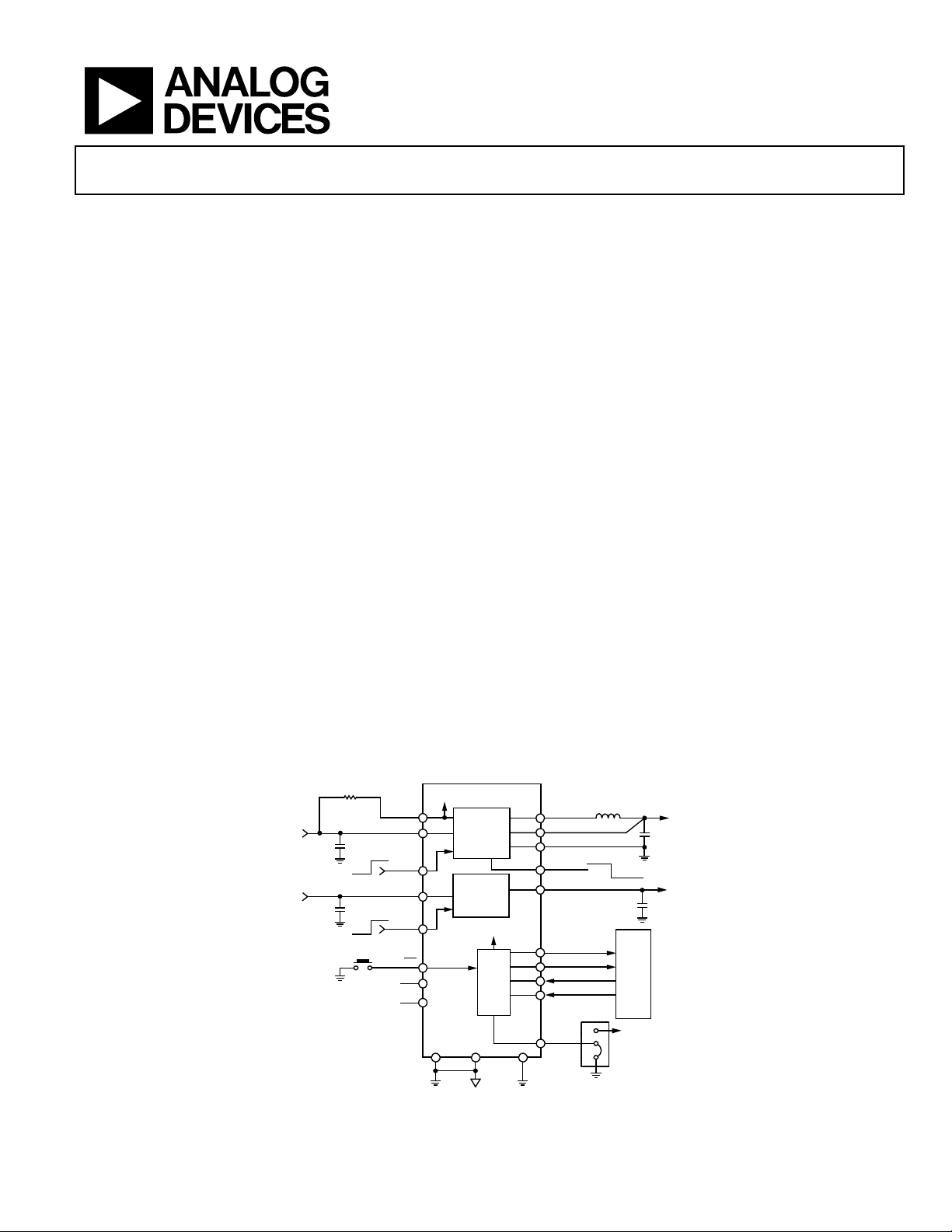
VIN
WD1 MODE
SELECTION
FPWM
PSM/PWM
MODE
SW
VOUT1
PGND
C6
10µF
L1
1µH
EN_BK
BUCK
EN_LDO
LDO
VIN1
EN1
VIN2
EN2
C2
1µF
VOUT2
GND GND
C5
4.7µF
ON
OFF
ON
OFF
NC
VIN1 = 2.3V
TO 5.5V
AVIN
R
FILT
30Ω
VIN2 = 1.7V
TO 5.5V
MR
C1
1µF
MICROPROCESSOR
SUPERVISOR
WSTAT
WMOD
WDI1
WDI2
nRSTO
NC
AGND
AVIN
AVIN
ADP5043
V
OUT1
@
800mA
V
OUT2
@
300mA
09682-001
Data Sheet
FEATURES
Input voltage range: 2.3 V to 5.5 V
One 800 mA buck regulator
One 300 mA LDO
20-lead, 4 mm × 4 mm LFCSP package
Initial regulator accuracy: ±1%
Overcurrent and thermal protection
Soft start
Undervoltage lockout
Open-drain processor reset with threshold monitoring
±1.5% threshold accuracy over the full temperate range
Guaranteed reset output valid to V
Dual watchdog for secure systems
Watchdog 1 controls reset
Watchdog 2 controls reset and regulators power cycle
Buck regulator key specifications
Current-mode topology for excellent transient response
3 MHz operating frequency
Uses tiny multilayer inductors and capacitors
Mode pin selects forced PWM or auto PFM/PSM modes
100% duty cycle low dropout mode
LDO key specifications
Low V
from 1.7 V to 5.5 V
IN
Stable with1 µF ceramic output capacitors
High PSRR, 60 dB up to 1 kHz/10 kHz
Low output noise
Low dropout voltage: 150 mV at 300 mA load
−40°C to +125°C junction temperature range
= 1 V
CC
GENERAL DESCRIPTION
The ADP5043 combines one high performance buck regulator
and one low dropout regulator (LDO) in a small 20-lead LFCSP
to meet demanding performance and board space requirements.
The high switching frequency of the buck regulator enables use
of tiny multilayer external components and minimizes board space.
The MODE pin selects the buck’s mode of operation. When set
to logic high, the buck regulator operates in forced PWM mode.
When the MODE pin is set to logic low, the buck regulator
operates in PWM mode when the load is around the nominal
value. When the load current falls below a predefined threshold,
the regulator operates in power save mode (PSM) improving
the light-load efficiency.
The low quiescent current, low dropout voltage, and wide input
voltage range of the ADP5043 LDO extend the battery life of
portable devices. The LDO maintains a power supply rejection
of greater than 60 dB for frequencies as high as 10 kHz while
operating with a low headroom voltage.
Each regulator is activated by a high level on the respective
enable pin. The ADP5043 is available with factory programmable
default output voltages and can be set to a wide range of options.
The ADP5043 contains supervisory circuits that monitor
power supply voltage levels and code execution integrity in
microprocessor-based systems. The ADP5043 also provides
power-on reset signals. An on-chip dual watchdog timer can
reset the microprocessor or power cycle the system (Watchdog 2)
if it fails to strobe within a preset timeout period.
Information furnished by Analog Devices is believed to be accurate and reliable. However, no
responsibility is assumed by Analog Devices for its use, nor for any infringements of patents or other
license is granted by implication or otherwise under any patent or patent rights of Analog Devices.
HIGH LEVEL BLOCK DIAGRAM
Figure 1.
One Technology Way, P.O. Box 9106, Norwood, MA 02062-9106, U.S.A.
Tel: 781.329.4700 www.analog.com
Page 2

ADP5043 Data Sheet
TABLE OF CONTENTS
Features .............................................................................................. 1
General Description ......................................................................... 1
High Level Block Diagram .............................................................. 1
Revision History ............................................................................... 2
Specifications ..................................................................................... 3
General Specifications ................................................................. 3
Supervisory Specifications .......................................................... 3
Buck Specifications ....................................................................... 5
LDO Specifications ...................................................................... 5
Input and Output Capacitor, Recommended Specifications .. 6
Absolute Maximum Ratings ............................................................ 7
Thermal Data ................................................................................ 7
Thermal Resistance ...................................................................... 7
ESD Caution .................................................................................. 7
Pin Configuration and Function Descriptions ............................. 8
Typical Performance Characteristics ............................................. 9
Theory of Operation ...................................................................... 16
Power Management Unit ........................................................... 16
Buck Section ................................................................................ 17
LDO Section ............................................................................... 18
Supervisory Section ................................................................... 18
Applications Information .............................................................. 21
Buck External Component Selection ....................................... 21
LDO Capacitor Selection .......................................................... 22
Supervisory Section ................................................................... 23
PCB Layout Guidelines .............................................................. 24
Power Dissipation/Thermal Considerations ............................. 25
Evaluation Board Schematics and Artwork ............................ 27
Suggested Layout ........................................................................ 27
Bill of Materials ........................................................................... 28
Application Diagram ................................................................. 28
Factory Programmable Options ................................................... 29
Outline Dimensions ....................................................................... 30
Ordering Guide .......................................................................... 30
REVISION HISTORY
10/11—Rev. 0 to Re v. A
Updated Outline Dimensions ....................................................... 30
Changes to Ordering Guide .......................................................... 30
11—Revision 0: Initial Version
4/
Rev. A | Page 2 of 32
Page 3

Data Sheet ADP5043
Option A
2.25
V
mV
SPECIFICATIONS
GENERAL SPECIFICATIONS
AVIN, VIN1 = (V
are enabled.
Table 1.
Parameter Symbol Test Conditions/Comments Min Typ Max Unit
AVIN UNDERVOLTAGE LOCKOUT UVLO
Input Voltage Rising UVLO
Option B 3.9 V
Input Voltage Falling UVLO
Option A 1.95 V
Option B 3.1 V
SHUTDOWN CURRENT I
ENx = GND, TJ = −40°C to +125°C 2 µA
Thermal Shutdown Threshold TSSD TJ rising 150 °C
Thermal Shutdown Hysteresis TS
ENx, WDIx, MODE, WMOD,
Input Logic High VIH 2.5 V ≤ AVIN ≤ 5.5 V 1.2 V
Input Logic Low VIL 2.5 V ≤ AVIN ≤ 5.5 V 0.4 V
Input Leakage Current (WMOD Excluded) V
ENx = AVIN or GND, TJ = −40°C to +125°C 1 µA
WMOD Input Leakage Current V
OPEN-DRAIN OUTPUTS
nRSTO, WSTAT Output Voltage VOL AVIN = 2.3 V to 5.5 V, I
Open-Drain Reset Output Leakage Current 1 µA
+ 0.5 V) or 2.3 V, whichever is greater, AVIN, VIN1 ≥ VIN2, TA = 25°C, unless otherwise noted. Regulators
OUT1
TJ = −40°C to +125°C
AVIN
AVINRISE
AVI NFAL L
ENx = GND 0.1 µA
GND-SD
20 °C
SD-HYS
MR
INPUTS
ENx = AVIN or GND 0.05 µA
I-LEAKAGE
I-LKG-WMOD
VWMOD = 3.6 V, TJ = −40°C to +125°C 50 µA
nRSTO/WSTAT
= 3 mA 30
SUPERVISORY SPECIFICATIONS
AVIN, VIN1 = full operating range, TJ = −40°C to +125°C, unless otherwise noted.
Table 2.
Parameter Min Typ Max Unit Test Conditions/Comments
SUPPLY
Supply Current (Supervisory Circuit Only) 45 55 µA AVIN = 5.5 V, EN1 = EN2 = VIN1
43 52 µA AVIN = 3.6 V, EN1 = EN2 = VIN1
RESET THRESHOLD ACCURACY VTH − 0.8% VTH VTH + 0.8% V TA = 25°C, sensed on VOUTx
VTH − 1.5% VTH VTH + 1.5% V TJ = −40°C to +125°C, sensed on V
RESET THRESHOLD TO OUTPUT DELAY
GLITCH IMMUNITY (t
UOD
)
RESET TIMEOUT PERIOD WATCHDOG1 (t
RP1
50 125 400 µs VTH = V
)
Option A 24 30 36 ms
Option B 160 200 240 ms
RESET TIMEOUT PERIOD WATCHDOG2 (t
) 3.5 5 7 ms
RP2
VCC TO RESET DELAY (tRD) 150 µs VIN1 falling at 1 mV/µs
REGULATORS SEQUENCING DELAY (tD1, tD2) 2 ms
WATCHDOG INPUTS
Watchdog 1 Timeout Period (t
)
WD1
Option A 81.6 102 122.4 ms
Option B 1.28 1.6 1.92 sec
− 50 mV
OUT
OUTx
Rev. A | Page 3 of 32
Page 4
ADP5043 Data Sheet
Option D
6.4 8 9.6
min
Option A
210 ms
MANUAL RESET INPUT
Parameter Min Typ Max Unit Test Conditions/Comments
Watchdog 2 Timeout Period (t
Option A 6 7.5 9 sec
Option B Watchdog 2 disabled
Option C 3.2 4 4.8 min
Option E 11.2 16 19.2 min
Option F 25.6 32 38.4 min
Option G 51.2 64 76.8 min
Option H 102.4 128 153.8 min
Watchdog 2 Power Off Period (t
Option B 400 ms
WDI1 Pulse Width 80 ns VIL = 0.4 V, VIH = 1.2 V
WDI2 Pulse Width 8 µs VIL = 0.4 V, VIH = 1.2 V
Watchdog Status Timeout Period (t
WDI1 Input Current (Source) 8 15 20 µA V
WDI1 Input Current (Sink) −30 −25 −14 µA V
WDI2 Internal Pull-Down 45 kΩ
)
WD2
)
POFF
) 11.2 sec
WDCLEAR
= VCC, time average
WDI1
= 0, time average
WDI1
MR Input Pulse Width
MR Glitch Rejection
MR Pull-Up Resistance
MR to Reset Delay
1 µs
220 ns
25 52 80 kΩ
280 ns V
= 5 V
CC
Rev. A | Page 4 of 32
Page 5

Data Sheet ADP5043
NFET, AVIN = VIN1 = 5 V
150
210
mΩ
OPERATING SUPPLY CURRENT (per LDO)
I
I
= 0 µA, VOUT = 3.3 V
15 µA
100 µA < I
< 300 mA
−2 +2
%
BUCK SPECIFICATIONS
AVIN, VIN1 = 3.6 V, V
for typical specifications, unless otherwise noted.
Table 3.
Parameter Test Conditions/Comments Min Ty p Max Unit
INPUT CHARACTERISTICS
Input Voltage Range (VIN1) 2.3 5.5 V
OUTPUT CHARACTERISTICS
Output Voltage Accuracy PWM mode, I
PSM mode −2 +2 %
PWM TO POWER SAVE MODE CURRENT THRESHOLD 100 mA
INPUT CURRENT CHARACTERISTICS
DC Operating Current I
Shutdown Current ENx = 0 V, TA = TJ = −40°C to +125°C 0.2 1.0 μA
SW CHARACTERISTICS
SW On Resistance PFET 180 240 mΩ
PFET, AVIN = VIN1 = 5 V 140 190 mΩ
NFET 170 235 mΩ
= 1.8 V, TJ = −40°C to +125°C for minimum/maximum specifications, L = 1 µH, C
OUT1
1
= 100 mA −1 +1 %
LOAD
VIN1 = 2.3 V to 5.5 V, PWM mode,
= 1 mA to 800 mA
I
LOAD
= 0 mA, device not switching 21 35 μA
LOAD
−3 +3 %
= 10 µF, and TA = 25°C
OUT
Current Limit PFET switch peak current limit 1100 1360 1600 mA
ACTIVE PULL-DOWN EN1 = 0 V 75 Ω
OSCILLATOR FREQUENCY 2.5 3.0 3.5 MHz
STA RT-UP TIME 250 μs
1
All limits at temperature extremes are guaranteed via correlation using standard statistical quality control (SQC).
LDO SPECIFICATIONS
AVIN = 3.6 V, VIN2 = (VOUT2 + 0.2 V) or 2.3 V, whichever is greater; AVIN, VIN1 ≥ VIN2; I
T
= 25°C, unless otherwise noted.
A
Table 4.
Parameter Symbol Test Conditions/Comments Min Typ Max Unit
INPUT VOLTAGE RANGE V
I
I
I
I
FIXED OUTPUT VOLTAGE ACCURACY V
TJ = −40°C to +125°C 1.7 5.5 V
IN2
GND
I
OUT2
OUT
= 0 µA, VOUT = 3.3 V,
I
OUT
= −40°C to +125°C
T
J
= 10 mA 67 µA
OUT
= 10 mA, TJ = −40°C to +125°C 105 µA
OUT
= 200 mA 100 µA
OUT
= 200 mA, TJ = −40°C to +125°C 245 µA
OUT
= 10 mA −1 +1 %
OUT
OUT
VIN2 = (VOUT2 + 0.5 V) to 5.5 V
100 µA < I
< 300 mA −3 +3 %
OUT
VIN2 = (VOUT2 + 0.5 V) to 5.5 V
TJ = −40°C to +125°C
= 10 mA; CIN = C
OUT
= 1 µF;
OUT
50 µA
Rev. A | Page 5 of 32
Page 6

ADP5043 Data Sheet
Load Regulation1
∆V
/∆I
= 1 mA to 200 mA
0.002
%/mA
DROPOUT VOLTAGE2
V
VOUT2 = 3.3 V
CAPACITOR ESR
R
TJ = −40°C to +125°C
0.001
1 Ω
Parameter Symbol Test Conditions/Comments Min Typ Max Unit
REGULATION
Line Regulation ∆V
I
TJ = −40°C to +125°C
I
TJ = −40°C to +125°C
I
I
I
I
ACTIVE PULL-DOWN R
STA RT-UP TIME T
CURRENT-LIMIT THRESHOLD3 I
OUTPUT NOISE OUT
POWER SUPPLY REJECTION RATIO PSRR
1
Based on an end-point calculation using 1 mA and 100 mA loads.
2
Dropout voltage is defined as the input-to-output voltage differential when the input voltage is set to the nominal output voltage. This applies only for output
voltages above 2.3 V.
3
Current-limit threshold is defined as the current at which the output voltage drops to 90% of the specified typical value. For example, the current limit for a 3.0 V
output voltage is defined as the current that causes the output voltage to drop to 90% of 3.0 V, or 2.7 V.
/∆V
OUT2
OUT2
DROPOUT
EN2 = 0 V 600 Ω
PDLDO
VOUT2 = 3.3 V 85 µs
STA RT-UP
TJ = −40°C to +125°C 335 470 mA
LIMIT
LDONOISE
VIN2= (VOUT2 + 0.5 V) to 5.5 V −0.03 +0.03 %/V
IN2
= 1 mA
OUT2
OUT2 IOUT2
= 1 mA to 200 mA 0.0075 %/mA
OUT2
= 10 mA 4 mV
OUT2
= 10 mA, TJ = −40°C to +125°C 5 mV
OUT2
= 200 mA 60 mV
OUT2
= 200 mA, TJ = −40°C to +125°C 100 mV
OUT2
10 Hz to 100 kHz, VIN2 = 5 V,
123 µV rms
VOUT2 = 3.3 V
10 Hz to 100 kHz, VIN2 = 5 V,
110 µV rms
VOUT2 = 2.8 V
10 Hz to 100 kHz, VIN2 = 5 V,
59 µV rms
VOUT2 = 1.5 V
1 kHz, VIN2 = 3.3 V, VOUT2 = 2.8 V,
I
= 100 mA
OUT
100 kHz, VIN2 = 3.3 V, VOUT2 = 2.8 V,
= 100 mA
I
OUT
1 MHz, VIN2 = 3.3 V, VOU T2 = 2.8 V,
= 100 mA
I
OUT
66 dB
57 dB
60 dB
INPUT AND OUTPUT CAPACITOR, RECOMMENDED SPECIFICATIONS
Table 5.
Parameter Symbol Test Conditions/Comments Min Ty p Max Unit
OUTPUT CAPACITANCE (BUCK)1 C
MINIMUM INPUT AND OUTPUT CAPACITANCE2 (LDO) C
1
The minimum output capacitance should be greater than 4.7 µF over the full range of operating conditions. The full range of operating conditions in the application
must be considered during device selection to ensure that the minimum capacitance specification is met.
2
The minimum input and output capacitance should be greater than 0.70 µF over the full range of operating conditions. The full range of operating conditions in the
application must be considered during device selection to ensure that the minimum capacitance specification is met. X7R and X5R type capacitors are recommended,
Y5V and Z5U capacitors are not recommended for use with LDOs or the buck.
TJ = −40°C to +125°C 7 40 µF
MIN1
TJ = −40°C to +125°C 0.70 µF
MIN2
ESR
Rev. A | Page 6 of 32
Page 7
Data Sheet ADP5043
ESD Machine Model
100 V
ABSOLUTE MAXIMUM RATINGS
Table 6.
Parameter Rating
AVIN, VINx, VOUTx, ENx, MODE, MR, WDIx,
WMOD, WSTAT, nRSTO to GND
Storage Temperature Range −65°C to +150°C
Operating Junction Temperature Range −40°C to +125°C
Soldering Conditions JEDEC J-STD-020
ESD Human Body Model 3000 V
ESD Charged Device Model 1500 V
−0.3 V to +6 V
Junction-to-ambient thermal resistance (θ
based on modeling and calculation using a 4-layer board. The
junction-to-ambient thermal resistance is highly dependent on
the application and board layout. In applications where high
maximum power dissipation exists, close attention to thermal
board design is required. The value of θ
PCB material, layout, and environmental conditions. The specified
value of θ
is based on a four-layer, 4” × 3”, 2.5 oz copper board,
JA
as per JEDEC standard. For additional information, see the
AN-772 Application Note, A Design and Manufacturing Guide
for the Lead Frame Chip Scale (LFCSP).
) of the package is
JA
may vary, depending on
JA
Stresses above those listed under absolute maximum ratings
may cause permanent damage to the device. This is a stress
rating only and functional operation of the device at these or
any other conditions above those indicated in the operational
section of this specification is not implied. Exposure to absolute
maximum rating conditions for extended periods may affect
device reliability.
THERMAL DATA
Absolute maximum ratings apply individually only, not in
combination.
The ADP5043 can be damaged when the junction temperature
limits are exceeded. Monitoring ambient temperature does not
guarantee that the junction temperature is within the specified
temperature limits. In applications with high power dissipation
and poor thermal resistance, the maximum ambient temperature may have to be derated. In applications with moderate
power dissipation and low PCB thermal resistance, the maximum
ambient temperature can exceed the maximum limit as long
as the junction temperature is within specification limits. The
junction temperature of the device is dependent on the ambient
temperature, the power dissipation of the device (P
junction-to-ambient thermal resistance of the package. Maximum junction temperature is calculated from the ambient
temperature and power dissipation using the formula
T
= TA + (PD × θJA)
J
), and the
D
THERMAL RESISTANCE
θJA is specified for the worst-case conditions, that is, a device
soldered in a circuit board for surface-mount packages.
Table 7. Thermal Resistance
Package Type θJA θJC Unit
20-Lead, 0.5 mm pitch LFCSP 38 4.2 °C/W
ESD CAUTION
Rev. A | Page 7 of 32
Page 8
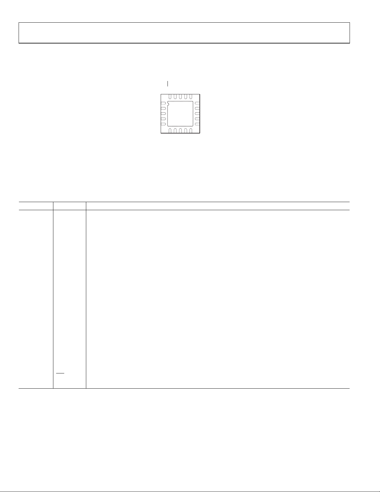
ADP5043 Data Sheet
NOTES
1. EXPOS E D P AD S HOULD BE CONNECT E D TO AGND.
2. NC = NO CONNECT. DO NOT CONNECT T O THIS PIN.
THE PIN SHOULD BE LEFT FLOATING.
14
13
12
1
3
4
NC
15
WSTAT
GND
WDI2
11
VOUT1
NC
VIN2
2
VOUT2
EN2
5
nRSTO
7
VIN1
6
AVIN
8
SW
9
PGND
10
EN1
19
WDI1
20
18 WMOD
17
MODE
16
GND
ADP5043
MR
TOP VIEW
(Not to S cale)
09682-002
5
nRSTO
Open-Drain Reset Output, Active Low.
11
VOUT1
Buck Sensing Node.
19
WDI1
Watchdog 1 Refresh Input from Processor. If WDI1 is in high-Z and WMOD is low, Watchdog 1 is disabled.
PIN CONFIGURATION AND FUNCTION DESCRIPTIONS
Figure 2. Pin Configuration
Table 8. Pin Function Descriptions
Pin No. Mnemonic Description
1 NC Do not connect to this pin. The pin should be left floating.
2 VOUT2 LDO Output Voltage and Sensing Input.
3 VIN2 LDO Input Supply (1.7 V to 5.5 V).
4 EN2 Enable LDO. EN2 = high: turn on the LDO; EN2 = low: turn off the LDO.
6 AVIN Regulators Housekeeping and Supervisory Input Supply (2.3 V to 5.5 V).
7 VIN1 Buck Input Supply (2.3 V to 5.5 V).
8 SW Buck Switching Node.
9 PGND Dedicated Power Ground for Buck Regulator.
10 EN1 Enable Buck. EN1 = high: turn on buck; EN1 = low: turn off buck.
12 WDI2 Watchdog 2 (Long Timeout) Refresh Input from Processor. This pin can be disabled only by a factory option.
13 GND Connect to the ground plane.
14 NC Do not connect to this pin. The pin should be left floating.
15 WS TAT
Open-Drain Watchdog Timeout Status. WSTAT = high: Watchdog 1 timeout or power-on reset; WSTAT = low:
Watchdog 2 timeout. Auto cleared after one second.
16 GND Connect to the ground plane.
17 MODE
Buck Mode. MODE = high: buck regulator operates in fixed PWM mode; MODE = low: (auto mode) buck
regulator operates in power save mode (PSM) at light load and in constant PWM at higher load.
18 WMOD
Watchdog Mode. WMOD = low: Watchdog 1 normal mode; WMOD = high: Watchdog 1 cannot be disabled by a
three-state condition applied on WDI1. WMOD has an internal 200 kΩ pull-down resistor connected to AGND.
20
MR
Manual Reset Input, Active Low.
TP AGND Analog Ground (TP = Exposed Thermal Pad). Exposed pad should be connected to AGND.
Rev. A | Page 8 of 32
Page 9
Data Sheet ADP5043
CH1 2.0V/DIV 1MΩ
B
W
20.0M
CH2 2.0V/DIV 1MΩ
B
W
20.0M
A CH1 1.76V 200µs/DIV
20.0ns/pt
1
2
VOUT1
VOUT2
09682-003
0
0.1
0.2
0.3
0.4
0.5
0.6
1.0
0.9
0.8
0.7
2.3 2.8 3.3 3.8 4.3 4.8 5.3
SYSTEM QUIESCENT CURRE NT (mA)
INPUT VOLTAGE (V)
V
OUT1
= 1.5V,
V
OUT2
= 3.3V
09682-004
CH1 2.0V/DIV 1MΩ
B
W
20.0M
CH2 2.0V/DIV 1MΩ
B
W
500M
CH3 100mA/DIV 1MΩ
B
W
20.0M
CH4 5.0V/DIV 1MΩ
B
W
500M
A CH1 2.92V 50µs/DIV
50.0MS/s
20.0ns/pt
2
4
1
3
SW
VOUT1
EN
IIN
09682-005
3.22
3.24
3.26
3.28
3.30
3.32
3.34
OUTPUT VOLTAGE (V)
OUTPUT CURRE NT (A)
0 0.1 0.2 0.3 0.4 0.5 0.6 0.7 0.8 0.9 1.0
+25°C
–40°C
+85°C
09682-007
1.775
1.780
1.785
1.790
1.795
1.800
1.805
1.810
1.815
1.820
1.825
1.830
0 0.1 0.2 0.3 0.4 0.5 0.6 0.7 0.8
OUTPUT CURRE NT (A)
OUTPUT VOLTAGE (V)
+25°C
–40°C
+85°C
09682-008
1.784
1.785
1.786
1.787
1.788
1.789
1.790
1.791
1.792
1.793
1.794
1.795
0 0.
1 0.2 0.3 0.4 0.5 0.6 0.7 0.8
–40°C
+25
°C
+85°C
OUTPUT CURRE NT (A)
OUTPUT VOLTAGE (V)
09682-009
TYPICAL PERFORMANCE CHARACTERISTICS
VIN1 = VIN2 = AVIN = 5.0 V, TA = 25°C, unless otherwise noted.
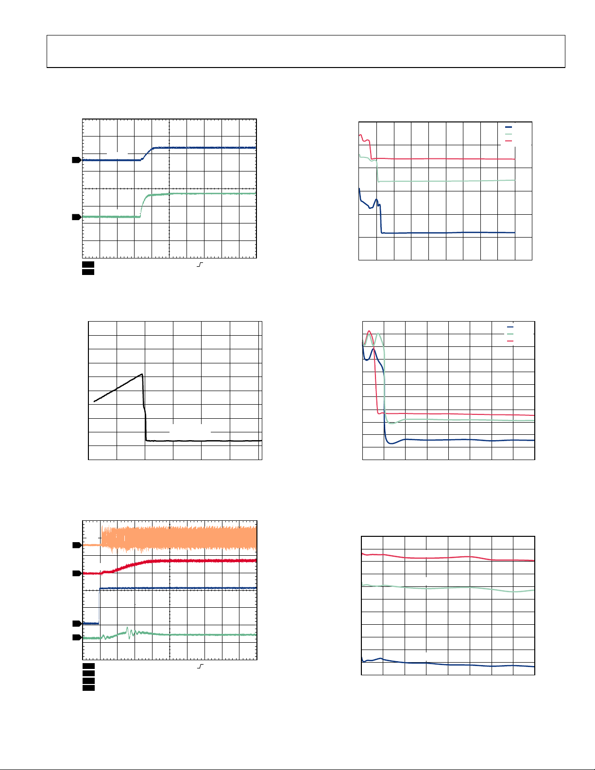
Figure 3. 3-Channel Start-Up Waveforms
Figure 4. System Quiescent Current (Sum of All the Input Currents) vs. Input
Voltage, V
OUT1
= 1.5 V, V
OUT2
= 3.3 V
Figure 6. Buck Load Regulation Across Temperature, V
Figure 7. Buck Load Regulation Across Temperature, V
= 3.3 V, Auto Mode
OUT1
= 1.8 V, Auto Mode
OUT1
Figure 5. Buck Startup, V
OUT1
= 1.8 V, I
OUT1
= 20 mA
Rev. A | Page 9 of 32
Figure 8. Buck Load Regulation Across Temperature, V
PWM Mode
OUT1
= 1.8 V,
Page 10
ADP5043 Data Sheet
1.790
1.791
1.792
1.793
1.794
1.795
1.796
1.797
0 0.
1 0.2 0.3 0.4 0.5 0.6 0.7 0.8
OUTPUT CURRE NT (A)
OUTPUT VOLTAGE (V)
VIN = 5.5V
VIN = 4.5V
V
IN
= 3.6V
09682-010
0
10
20
30
40
50
60
70
80
90
100
0.0001 0.001 0.01 0.1 1
EFFICIENCY (%)
OUTPUT CURRE NT (A)
3.6V
4.5V
5.5V
09682-011
0
10
20
30
40
50
60
70
80
90
100
0.001 0.01 0.1 1
EFFICIENCY (%)
OUTPUT CURRE NT (A)
3.6V
4.5V
5.5V
09682-012
0
10
20
30
40
50
60
70
80
90
100
0.0001 0.001 0.01 0.1 1
EFFICIENCY (%)
OUTPUT CURRE NT (A)
2.4V
3.6V
4.5V
5.5V
09682-013
0
10
20
30
40
50
60
70
80
90
100
0.001 0.
01 0.1 1
EFFICIENCY (%)
OUTPUT CURRE NT (A)
2.4V
3.6V
4.5V
5.5V
09682-014
0
10
20
30
40
50
60
70
80
90
100
0.001 0.01 0.1 1
EFFICIENCY (%)
OUTPUT CURRE NT (A)
+25°C
–40°C
+85°C
09682-015
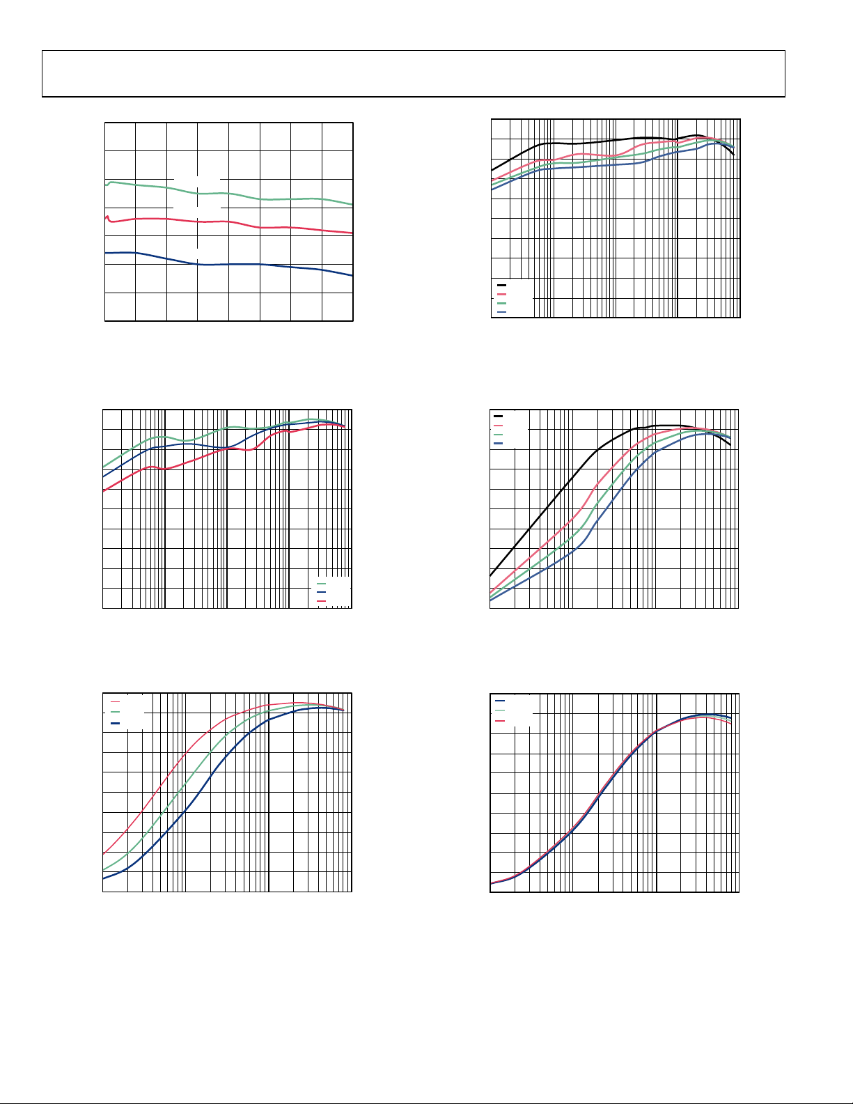
Figure 9. Buck Load Regulation Across Input Voltage, V
OUT1
= 1.8 V,
PWM Mode
Figure 10. Buck Efficiency vs. Load Current, Across Input Voltage,
= 3.3 V, Auto Mode
V
OUT1
Figure 12. Buck Efficiency vs. Load Current, Across Input Voltage,
= 1.8 V, Auto Mode
V
OUT1
Figure 13. Buck Efficiency vs. Load Current, Across Input Voltage,
= 1.8 V, PWM Mode
V
OUT1
Figure 11. Buck Efficiency vs. Load Current, Across Input Voltage,
= 3.3 V, PWM Mode
V
OUT1
Figure 14. Buck Efficiency vs. Load Current, Across Temperature, V
OUT1
= 1.8 V,
PWM Mode
Rev. A | Page 10 of 32
Page 11

Data Sheet ADP5043
0
10
20
30
40
50
60
70
80
90
100
0.0001 0.001 0.01 0.1 1
EFFICIENCY (%)
OUTPUT CURRE NT (A)
+25°C
–40°C
+85°C
09682-016
0
10
20
30
40
50
60
70
80
90
100
0.0001 0.001 0.01 0.
1 1
EFFICIENCY (%)
OUTPUT CURRE NT (A)
+25°C
–40°C
+85°C
09682-017
1.7
1.6
1.5
1.4
1.3
1.2
1.1
1.0
2.6 3.6 4.6 5.6
INPUT VOLTAGE (V)
OUTPUT CURRE NT (A)
09682-018
2.85
2.90
2.95
3.00
3.05
3.10
0 0.1 0.2 0.3 0.4 0.5 0.6 0.7 0.8
FREQUENCY (MHz)
+25°C
–40°C
+85°C
OUTPUT CURRE NT (A)
09682-019
CH1 20.0mV/ DIV
B
W
20.0M
CH2 200mA/DIV 1MΩ
B
W
20.0M
CH3 2.0V/ DIV 1MΩ
B
W
20.0M
A CH1 2.4mV 5.0µs/DIV
20.0MS/s
50.0ns/pt
1
2
3
VOUT
I
SW
SW
09682-020
CH1 2.0V/DIV 1MΩ
B
W
20.0M
CH2 50.0mV/ DIV
B
W
20.0M
CH3 500mA/DIV
B
W
20.0M
A CH1 1.56mV 5.0µs/DIV
200MS/s
5.0ns/pt
2
3
1
VOUTx
I
SW
SW
09682-021
Figure 15. Buck Efficiency vs. Load Current, Across Temperature, V
Auto Mode
Figure 16. Buck Efficiency vs. Load Current, Across Temperature, V
Auto Mode
OUT1
OUT1
= 3.3 V,
= 1.8 V,
Figure 18. Buck Switching Frequency vs. Output Current, Across
Temperature, V
Figure 19. Typical Waveforms, V
= 1.8 V, PWM Mode
OUT1
= 3.3 V, I
OUT1
= 30 mA, Auto Mode
OUT1
Figure 17. Buck DC Current Capability vs. Input Voltage, V
OUT1
= 1.8 V
Figure 20. Typical Waveforms, V
OUT1
= 1.8 V, I
= 30 mA, Auto Mode
OUT1
Rev. A | Page 11 of 32
Page 12

ADP5043 Data Sheet
CH1 2.0V/DIV 1MΩ
B
W
20.0M
CH2 50.0mV/ DIV
B
W
20.0M
CH3 500mA/DIV
B
W
20.0M
A CH1 1.56mV 500ns/DIV
200MS/s
5.0ns/pt
2
3
1
VOUTx
I
SW
SW
09682-022
CH1 20.0mV/ DIV
B
W
20.0M
CH2 200mA/DIV 1MΩ
B
W
20.0M
CH3 2.0V/DIV 1MΩ
B
W
20.0M
A CH1 2.4mV 200ns/DIV
500MS/s
2.0ns/pt
1
2
3
VOUTx
I
SW
SW
09682-023
CH1 3V/DI V
B
W
20.0M
CH2 50mV/DI V
B
W
20.0M
CH3 900mV/DIV 1MΩ
B
W
20.0M
A CH3 4.79V 100µs/DIV
10.0MS/s
100ns/pt
1
3
VINx
VOUTx
SW
2
09682-024
CH2 50mV/DI V
B
W
20.0M
CH3 1V/DI V 1MΩ
B
W
20.0M
CH4 2V/DI V 1MΩ
B
W
20.0M
A CH3 4.96mV 100µs/DIV
20MS/s
100ns/pt
2
3
4
VINx
VOUTx
SW
09682-025
CH1 4V/DI V
B
W
20.0M
CH2 50mV/DI V 1MΩ
B
W
20.0M
CH3 50mA/DIV 1M Ω
B
W
20.0M
A CH3 44mA 200µ
s/DIV
10MS/s
100ns/pt
2
3
1
SW
VOUTx
IOUT
09682-026
CH1 4V/DI V
B
W
20.0M
CH2 50mV/DI V
B
W
20.0M
CH3 50mA/DIV 1M Ω
B
W
20.0M
A CH3 28mA 200µs/DIV
5MS/s
200ns/pt
2
3
1
VOUTx
SW
V
OUT
LOAD
09682-027
Figure 21. Typical Waveforms, V
Figure 22. Typical Waveforms, V
OUT1
OUT1
= 1.8 V, I
= 3.3 V, I
= 30 mA, PWM Mode
OUT1
= 30 mA, PWM Mode
OUT1
Figure 24. Buck Response to Line Transient, VIN = 4.5 V to 5.0 V, V
PWM Mode
Figure 25. Buck Response to Load Transient, I
= 3.3 V, Auto Mode
V
OUT1
from 1 mA to 50 mA,
OUT1
OUT1
= 1.8 V,
Figure 23. Buck Response to Line Transient, Input Voltage from 4.5 V to 5.0 V,
= 3.3 V, PWM Mode
V
OUT1
Figure 26. Buck Response to Load Transient, I
= 1.8 V, Auto Mode
V
OUT1
from 1 mA to 50 mA,
OUT2
Rev. A | Page 12 of 32
Page 13

Data Sheet ADP5043
A CH3 86mA
2
3
1
VOUTx
SW
LOAD
CH1 4V/DI V
B
W
20.0M
CH2 50mV/DIV
B
W
20.0M
CH3 50mA/DI V 1MΩ
B
W
20.0M
200µs/DIV
10MS/s
100ns/pt
09682-028
3
4
2
VOUT1
LOAD
SW
CH2 4V/DI V 1MΩ
B
W
20.0M
CH3 50mV/DI V 1MΩ
B
W
20.0M
CH4 50mA/DIV 1MΩ
B
W
20.0M
200µs/DIV
50MS/s
20ns/pt
A CH3 145mA
09682-029
1
2
3
VOUTx
I
IN
EN
A CH2 1.14V
CH1 1V/DI V 1MΩ
B
W
500M
CH2 3V/DIV 1MΩ
B
W
500M
CH3 50mA/DI V 1MΩ
B
W
20.0M
100µs/DIV
1MS/s
1.0µs/pt
09682-031
3.25
3.26
3.27
3.28
3.29
3.30
3.31
3.
32
3.33
3.34
3.35
0.0001 0.001 0.01 0.1
OUTPUT VOLTAGE (V)
OUTPUT CURRE NT (A)
3.6V
4.5V
5.0V
5.5V
09682-035
3.25
3.26
3.27
3.28
3.29
3.30
3.31
3.32
3.33
3.34
3.35
0.0001 0.001 0.01 0.1
OUTPUT VOLTAGE (V)
OUTPUT CURRE NT (A)
+85°C
+25°C
–40°C
09682-036
3.280
3.285
3.290
3.295
3.300
3.305
3.310
3.315
3.320
3.325
3.5 4.5 5.0 5.5
OUTPUT VOLTAGE (V)
INPUT VOLTAGE (V)
100µA
1mA
10mA
100mA
150mA
09682-037
Figure 27. Buck Response to Load Transient, I
= 3.3 V, Auto Mode
V
OUT1
Figure 28. Buck Response to Load Transient, I
= 1.8 V, PWM Mode
V
OUT1
from 20 mA to 140 mA,
OUT1
= 20 mA to 180 mA,
OUT1
Figure 30. LDO Load Regulation Across Input Voltage, V
Figure 31. LDO Load Regulation Across Temperature, V
= 3.3 V
V
OUT2
= 3.3 V
OUT2
= 3.6 V,
IN2
Figure 29. LDO Startup, V
OUT2
= 3.3 V, I
OUT2
= 5 mA
Rev. A | Page 13 of 32
Figure 32. LDO Line Regulation Across Output Load, V
OUT2
= 3.3 V
Page 14

ADP5043 Data Sheet
0 0.05 0.10 0.15
LOAD (A)
CURRENT (µA)
0
50
100
150
200
250
09682-038
0
0.05
0.10
0.15
0.20
0.25
0.30
0.35
0.40
0.45
0.50
2.3 2.8 3.3 3.8 4.3 4.8 5.3 5.8
GROUND CURRENT ( mA)
INPUT VOLTAGE (V)
1µA
100µA
1mA
10mA
100mA
150mA
09682-039
3
1
VOUT
IOUT
CH1 50mV/DI V 1MΩ
B
W
500M
CH3 50mA/DIV 1M Ω
B
W
20.0M
200µs/DIV
500kS/s
2.0µs/pt
A CH3 28mA
09682-040
21
2
2
CH1 10.0mV/DIV
CH2 800mV/DIV
A CH2 5.33V
1MΩ
B
W
20.0M
VOUT
VIN
B
W
20.0M
09682-042
LOAD CURRENT ( A)
OUTPUT VOLTAGE (V)
0 0.1 0.2 0.3
0.5
0
1.0
1.5
2.0
2.5
3.0
0.4 0.5 0.6 0.7 0.8
5.5V
4.5V
3.6V
09682-056
LOAD (mA)
RMS NOISE (µV)
100
10
V
OUT
= 3.3V; VIN = 5V
V
OUT
= 3.3V; VIN = 3.6V
V
OUT
= 2.8V; VIN = 3.1V
V
OUT
= 1.5V; V
IN
= 5V
V
OUT
= 1.5V; V
IN
= 1.8V
0.0001 0.001 0.01 0.1 1 10 100 1k
09682-045
Figure 33. LDO Ground Current vs. Output Load, V
OUT2
= 2.8 V
Figure 34. LDO Ground Current vs. Input Voltage, Across Output Load,
= 2.8 V
V
OUT2
Figure 36. LDO Response to Line Transient, V
= 4.5 V to 5.5 V, V
IN2
Figure 37. LDO Output Current Capability vs. Output Voltage
OUT2
= 3.3 V
Figure 35. LDO Response to Load Transient, I
= 3.3 V
V
OUT2
from 1 mA to 80 mA,
OUT2
Figure 38. LDO Output Noise vs. Load Current, Across Input and Output Voltage
Rev. A | Page 14 of 32
Page 15

Data Sheet ADP5043
V
OUT2
= 3.3V, V
IN2
= 3.6V, I
LOAD
= 300mA
V
OUT2
= 1.5V, V
IN2
= 1.8V, I
LOAD
= 300mA
V
OUT2
= 2.8V, V
IN2
= 3.1V, I
LOAD
= 300mA
NOISE (µV/√Hz)
100
10
1
0.1
0.01
1 10 100 1k
FREQUENCY ( Hz )
10k 100k 1M
09682-055
–10
–20
–30
–40
–50
–60
–70
–80
–90
–100
10 100 1k
10k 100k 1M 10M
F
REQUENCY (Hz)
PSRR (dB)
1mA
10mA
100mA
200mA
300mA
09682-049
–10
–20
–30
–40
–50
–60
–70
–80
–90
–100
10 100 1k 10k 100k
1M 10M
F
REQUENCY (Hz)
PSRR (dB)
1mA
10mA
100mA
200mA
300mA
09682-050
–10
–20
–30
–40
–50
–60
–70
–80
–90
–100
10 100 1k
10k 100k 1M 10M
F
REQUENCY (Hz)
PSRR (dB)
1mA
10mA
100mA
200mA
09682-051
Figure 39. LDO Output Noise Spectrum, Across Input and Output Voltage
Figure 40. LDO PSRR Across Output Load, V
= 3.3 V, V
IN2
OUT2
= 2.8 V
Figure 41. LDO PSRR vs. Frequency, V
Figure 42. LDO PSRR vs. Frequency, V
= 3.1 V, V
IN2
= 5 V, V
IN2
OUT2
OUT2
= 2.8 V
= 3.3 V
Rev. A | Page 15 of 32
Page 16

ADP5043 Data Sheet
SOFT START
PWM/PSM
CONTROL
BUCK1
DRI
VER
AND
ANTISHOOT
THROUGH
OSCILLATOR
V
REF
THERMAL
SHUTDOWN
SYSTEM
UNDERVOLTAGE
LOCK OUT
RESET
GENERATOR
DEBOUNCE
PWM
COMP
VDDA
VDDA
GM ERROR
AMP
PSM
COMP
LOW
CURRENT
I
LIMIT
ADP5043
VOUT1 WMOD
ENWD1 E
NWD2
VIN1
AVIN
SW
PGND
EN1
ENBK
ENLDO
MODE
MODE
EN2
SEL
OPMODE_FUSES
AGND VIN2
LDO
CONTROL
R1
R2
ENBK
75Ω
ENLDO
600Ω
C
B Y
A
VDDA
R0 R1
MR
WDI1
200kΩ
VDDA
52kΩ
40kΩ
WATCHDOG
STATUS
MONITOR
WDI2
POFF
POFF
VOUT2
nRSTO
WSTAT
ENABLE
AND MODE
CONTROL
WATCHDOG
DETECTOR1
WATCHDOG
DETECTOR2
09682-057
THEORY OF OPERATION
POWER MANAGEMENT UNIT
The ADP5043 is a micro power management unit (micro PMU)
Figure 43. Functional Block Diagram
combing one step-down (buck) dc-to-dc regulator, one low
dropout linear regulator (LDO), and a supervisory circuit, with
dual watchdog, for processor control. The regulators are activated
by a logic level high applied to the respective EN pins. EN1
controls the buck regulator while EN2 controls the LDO. The
ADP5043 has factory programmed output voltages and reset
voltage threshold. Other features available in this device are the
MODE pin to control the buck switching operation, a status pin
(WSTAT) informing the external processor which watchdog
caused a reset, and a push-button reset input (nRSTO).
When a regulator is turned on, the output voltage is controlled
through a soft start circuit, which prevents a large inrush current
due to the discharged output capacitors.
The buck regulator can operate in forced PWM mode if the
MODE pin is at a logic high level. In forced PWM mode, the
switching frequency of the buck is always constant and does not
change with the load current. If the MODE pin is at a logic low
level, the switching regulator operates in auto PWM/PSM mode.
In this mode, the regulator operates at fixed PWM frequency
when the load current is above the power saving current threshold.
When the load current falls below the power saving current
threshold, the regulator enters power saving mode where the
switching occurs in bursts. The burst repetition rate is a
function of the current load and the output capacitor value.
This operating mode reduces the switching and quiescent
current losses.
Rev. A | Page 16 of 32
Page 17

Data Sheet ADP5043
Thermal Protection
In the event that the junction temperature rises above 150°C,
the thermal shutdown circuit turns off the buck and LDO.
Extreme junction temperatures can be the result of high current
operation, poor circuit board design, or high ambient temperature.
A 20°C hysteresis is included in the thermal shutdown circuit
so that if thermal shutdown occurs, the buck and LDO do not
return to normal operation until the on-chip temperature drops
below 130°C. When coming out of thermal shutdown, a soft
start is initiated.
Undervoltage Lockout
To protect against battery discharge, undervoltage lockout
(UVLO) circuitry is integrated in the ADP5043. If the input
voltage on AVIN drops below a typical 2.15 V UVLO threshold,
all channels shut down. In the buck channel, both the power
switch and the synchronous rectifier turn off. When the voltage
on AVIN rises above the UVLO threshold, the part is enabled
once more.
Alternatively, the user can select device models with a UVLO
set at a higher level, suitable for 5 V applications. For these
models, the device hits the turn-off threshold when the input
supply drops to 3.65 V typical.
Enable/Shutdown
The ADP5043 has individual control pins for each regulator. A
logic level high applied to the ENx pin activates a regulator; a
logic level low turns off a regulator.
When regulators are turned off after a Watchdog 2 event (see
the Watchdog 2 Input section), the reactivation of the regulator
occurs with a factory programmed order (see Tabl e 9). The
delay between the regulator activation (
Table 9. ADP5043 Regulators Sequencing
REGSEQ[1:0] Regulators Sequence (First to Last)
0 0 LDO to buck
0 1 Buck to LDO
1 0 Buck to LDO
1 1 No sequence, all regulators start at same time
t
, tD2) is 2 ms.
D1
BUCK SECTION
The buck uses a fixed frequency and high speed current-mode
architecture. The buck operates with an input voltage of 2.3 V
to 5.5 V.
Control Scheme
The buck operates with a fixed frequency current-mode PWM
control at medium to high loads for high efficiency; operation
shifts to a power save mode (PSM) control scheme at light loads
to lower the regulation power losses. When operating in fixed
frequency PWM mode, the duty cycle of the integrated switch is
adjusted to regulate the output voltage. When operating in PSM
at light loads, the output voltage is controlled in a hysteretic
manner that produces a higher output voltage ripple. During
part of this time, the converter is able to stop switching and
enters an idle mode, which improves conversion efficiency.
PWM Mode
In PWM mode, the buck operates at a fixed frequency of 3 MHz,
set by an internal oscillator. At the start of each oscillator cycle,
the high-side PFET switch is turned on, sending a positive
voltage across the inductor. Current in the inductor increases
until the current sense signal crosses the peak inductor current
threshold that turns off the PFET switch and turns on the lowside NFET synchronous rectifier. This sends a negative voltage
across the inductor, causing the inductor current to decrease.
The synchronous rectifier stays on for the rest of the cycle. The
buck regulates the output voltage by adjusting the peak inductor
current threshold.
Power Save Mode (PSM)
The buck smoothly transitions to PSM operation when the load
current decreases below the PSM current threshold. When the
buck enters power save mode, an offset is induced in the PWM
regulation level, which makes the output voltage rise. When the
output voltage reaches a level that is approximately 1.5% above
the PWM regulation level, PWM operation is turned off. At this
point, both power switches are off, and the buck enters an idle
state. The output capacitor discharges until the output voltage
falls to the PWM regulation voltage, at which point the device
drives the inductor to make the output voltage rise again to the
upper threshold. This process is repeated while the load current
stays below the PSM current threshold.
PSM Current Threshold
The PSM current threshold is set to 100 mA. The buck employs
a scheme that enables this current to remain accurately controlled, independent of input and output voltage levels. This
scheme also ensures that there is very little hysteresis between
the PSM current threshold for entry to, and exit from, the PSM
mode. The PSM current threshold is optimized for high
efficiency over all load currents.
Short-Circuit Protection
The buck includes frequency foldback to prevent current
runaway with a hard short on the output. When the voltage
at the feedback pin falls below half the target output voltage,
indicating the possibility of a hard short at the output, the
switching frequency is reduced to half the internal oscillator
frequency. The reduction in the switching frequency allows
more time for the inductor to discharge, preventing a runaway
of output current.
Soft Start
The buck has an internal soft start function that ramps the
output voltage in a controlled manner upon startup, thereby
limiting the inrush current. This prevents possible input
voltage drops when a battery or a high impedance power
source is connected to the input of the converter.
Rev. A | Page 17 of 32
Page 18

RSTO
nRSTO
t
RD
t
RD
t
RP1
t
RP1
VOUT2
V
TH
V
TH
0V
1V
0V
1V
0V
09682-058
ADP5043 Data Sheet
Current Limit
The buck has protection circuitry to limit the amount of
positive current flowing through the PFET switch and the
amount of negative current flowing through the synchronous
rectifier. The positive current limit on the power switch limits
the amount of current that can flow from the input to the
output. The negative current limit prevents the inductor
current from reversing direction and flowing out of the load.
100% Duty Operation
With a dropping input voltage or with an increase in load
current, the buck may reach a limit where, even with the PFET
switch on 100% of the time, the output voltage drops below the
desired output voltage. At this limit, the buck transitions to a
mode where the PFET switch stays on 100% of the time. When
the input conditions change again and the required duty cycle
falls, the buck immediately restarts PWM regulation without
allowing overshoot on the output voltage.
LDO SECTION
The ADP5043 contains one LDO with a low quiescent current
that provides an output current up to 300 mA. The low, 15 μA
typical, quiescent current at no load makes the LDO ideal for
battery-operated portable equipment.
The LDO operates with an input voltage range of 1.7 V to
5.5 V. The wide operating range makes this LDO suitable for
a cascade configuration where the LDO supply voltage is
provided from the buck regulator.
The LDO also provides high power supply rejection ratio (PSRR),
low output noise, and excellent line and load transient response
with a small 1 µF ceramic input and output capacitors.
The LDO is optimized to supply analog circuits by offering
better noise performance than the buck regulator.
Inter n a l l y, an LDO consists of a reference, an error amplifier,
a feedback voltage divider, and a PMOS pass transistor. Output
current is delivered via the PMOS pass device, which is controlled by the error amplifier. The error amplifier compares
the reference voltage with the feedback voltage from the output
and amplifies the difference. If the feedback voltage is lower
than the reference voltage, the gate of the PMOS device is
pulled lower, allowing more current to flow and increasing
the output voltage. If the feedback voltage is higher than the
reference voltage, the gate of the PMOS device is pulled higher,
reducing the current flowing to the output.
SUPERVISORY SECTION
The ADP5043 provides microprocessor supply voltage supervision by controlling the reset input of the microprocessor.
Code execution errors are avoided during power-up, powerdown, and brownout conditions by asserting a reset signal when
the supply voltage is below a preset threshold and by allowing
supply voltage stabilization with a fixed timeout reset pulse
after the supply voltage rises above the threshold. In addition,
Rev. A | Page 18 of 32
problems with microprocessor code execution can be monitored
and corrected with a dual-watchdog timer.
Reset Output
The ADP5043 has an active-low, open-drain reset output. This
output structure requires an external pull-up resistor to connect
the reset output to a voltage rail that is no higher than 6 V. The
resistor should comply with the logic low and logic high voltage
level requirements of the microprocessor while supplying input
current and leakage paths on the nRSTO pin. A 10 kΩ pull-up
resistor is adequate in most situations.
The reset output is asserted when the monitored rail is below
the reset threshold (V
within the watchdog timeout period (t
), when WDI1 or WDI2 is not serviced
TH
WD1
and t
). Reset remains
WD2
asserted for the duration of the reset active timeout period (t
after the monitored rail rises above the reset threshold or after
the watchdog timer times out. Figure 44 illustrates the behavior
of the reset output, nRSTO, and it assumes that VOUT2 is
selected as the rail to be monitored and supplies the external pullup connected to the nRSTO output.
Figure 44. Reset Timing Diagram
The reset threshold voltage and the sensed rail (VOUT1, VOUT2,
or AVI N ) are factory programmed. Refer to Ta b le 16 for a
complete list of the reset thresholds available for the ADP5043.
When monitoring the input supply voltage, AVIN, if the
selected reset threshold is below the UVLO level (factory
programmable to 2.25 V or 3.6 V) the reset output, nRSTO,
is asserted low as soon as the input voltage falls below the
UVLO threshold. Below the UVLO threshold, the reset output
is maintained low down to ~1 V VIN. This is to ensure that the
reset output is not released when there is sufficient voltage on the
rail supplying a processor to restart the processor operations.
Manual Reset Input
The ADP5043 features a manual reset input (MR) which, when
driven low, asserts the reset output. When
MR
transitions from
low-to-high, reset remains asserted for the duration of the reset
active timeout period before deasserting. The
MR
input has a
52 kΩ, internal pull-up, connected to AVIN, so that the input
is always high when unconnected. An external push-button
switch can be connected between
MR
and ground so that the
user can generate a reset. Debounce circuitry for this purpose is
integrated on chip. Noise immunity is provided on the
MR
input,
and fast, negative-going transients of up to 100 ns (typical) are
ignored. A 0.1 µF capacitor between
MR
and ground provides
additional noise immunity.
)
RP
Page 19

Data Sheet ADP5043
WDI1
n
RSTO
t
RP1
t
RP1
t
WD1
V
SENSED
V
TH
1V
0V
0V
0V
09682-059
AVIN/VINx/ENx
VOUT1
VOUT2
nRSTO
WDI2
WSTAT
V
TH
0V
0V
0V
0V
t
POFF
t
D1
t
D2
t
D1
t
RP1
t
RP2
t
RP1
t
WDCLEAR
t
D2
t
WD2
09682-060
Watchdog 1 Input
The ADP5043 features a watchdog timer that monitors
microprocessor activity. The watchdog timer circuit is cleared
with every low-to-high or high-to-low logic transition on the
watchdog input pin (WDI1), which detects pulses as short as
80 ns. If the timer counts through the preset watchdog timeout
period (t
), an output reset is asserted. The microprocessor is
WD1
required to toggle the WDI1 pin to avoid being reset. Failure of
the microprocessor to toggle WDI1 within the timeout period,
therefore, indicates a code execution error, and the reset pulse
generated restarts the microprocessor into a known state.
As well as logic transitions on WDI1, the watchdog timer is also
cleared by a reset assertion due to an undervoltage condition on
the monitored rail. When reset is asserted, the watchdog timer
is cleared and does not begin counting again until reset deasserts.
Watchdog 1 timer can be disabled by leaving WDI1 floating or
by three-stating the WDI1 driver. The pin WMOD controls the
Watchdog 1 operating mode. If WMOD is set to logic level low,
Watchdog 1 is enabled as long as WDI1 is not in three-state. If
WMOD is set to logic level high, Watchdog 1 is always active
and cannot be disabled by a three-state condition. WMOD
input has an internal 200 kΩ pull-down resistor.
Watchdog 1 timeout is factory set to two possible values, as
indicated in Table 18.
Watchdog 2 Input
The ADP5043 features an additional watchdog timer that
monitors microprocessor activity in parallel with the first watchdog
but with a much longer timeout. This provides additional security
and safety in case Watchdog 1 is incorrectly strobed. A timer
circuit is cleared with every low-to-high or high-to-low logic
transition on the watchdog input pin (WDI2), which detects pulses
as short as 8 µs. If the timer counts through the preset watchdog
timeout period (t
), reset is asserted, followed by a power
WD2
cycle of all regulators. The microprocessor is required to toggle
the WDI2 pin to avoid being reset and powered down. Failure
of the microprocessor to toggle WDI2 within the timeout period,
therefore, indicates a code execution error, and the reset output
nRSTO is forced low for
off for the t
time. After the t
POFF
t
. Then, all the regulators are turned
RP2
period, the regulators are
POFF
reactivated according to a predefined sequence (see Tab le 9).
Finally, the reset line (nRSTO) is asserted for
t
. This guaran-
RP1
tees a clean power-up of the system and proper reset.
As well as logic transitions on WDI2, the watchdog timer is
also cleared by a reset assertion due to an undervoltage condition
on the V
monitored rail which can be factory programmable
TH
between VOUT1, VOUT2, and AV I N (see Ta b l e 21). When
reset is asserted, the watchdog timer is cleared and does not
begin counting again until reset deasserts.
Watchdog 2 timeout is factory set to seven possible values as
indicated in Table 19. One additional option allows Watchdog 2
to be factory disabled.
Figure 45. Watchdog 1 Timing Diagram
Figure 46. Watchdog 2 Timing Diagram (Assuming That VOUT2 Is the Monitored Rail)
Rev. A | Page 19 of 32
Page 20

ADP5043 Data Sheet
NO POWER APPLIED TO AVIN.
ALL REGULATORS AND SUPERVISORY
TURNED OFF
NO POWER
POR
STANDBY
WSTAT = HIGH
WSTAT = HIGH
RESET
NORMAL
WSTAT = LOW
AVIN < VUVLO
ALL ENx = LOW
AVIN > VUVLO
TRANSITION
STATE
TRANSITION
STATE
TRANSITION
STATE
END OF POR
WSTAT
TIMEOUT
(t
WDCLEAR
)
WSTAT = 1
TRANSITION
STATE
ALL REGULATORS AND
SUPERVISOR ACTIVATED
WDOG2
TIMEOUT
(t
WD2
)
WSTAT = 0
END OF (t
POFF
)
PULSE
WDOG1 TIMEOUT
(t
WD1
) AND
WSTAT TIMEOUT
WSTAT = 1
WDOG1 TIMEOUT
(t
WD1
)
ALL ENx = HIGH
ACTIVE
POWER OFF
RESET SHORT
AVIN < VUVLO
END OF RESET
PULSE (t
RP2
)
INTERNAL CIRCUIT BIASED
REGULATORS AND
SUPERVISORY NOT ACTIVATED
AVIN < VUVLO
AVIN < VUVLO
VMON < VTH
END OF RESET
PULSE (t
RP1
)
09682-061
Watchdog Status Indicator
In addition to the dual watchdog function, the ADP5043
features a watchdog status monitor available on the WSTAT pin.
This pin can be queried by the external processor to determine
the origin of a reset. WSTAT is an open-drain output.
WSTAT outputs a logic level depending on the condition
that has generated a reset. WSTAT is forced low if the reset
was generated because of a Watchdog 2 timeout. WSTAT is
pulled high, through external pull-up, for any other reset cause
(Wat c hdog 1 timeout, power failure or monitored voltage be
low threshold). The status monitor is automatically cleared
(set to logic level high) 10 seconds after the nRSTO low-to-high
transition (t
to read the WSTAT flag before t
). The processor firmware must be designed
WDCLEAR
expiration after a
WDCLEAR
Watch d og 2 reset.
The WSTAT flag is not updated in the event of a reset due to a
low voltage threshold detection or Watchdog 1 event occurring
within 10 seconds after an nRSTO low-to-high transition. In
this situation, WSTAT maintains the previous state (see the state
flow in Figure 47).
The external processor can further distinguish a reset caused
by a Watchdog 1 timeout from a power failure, status monitor
WSTAT indicating a high level, by implementing a RAM check
or signature verification after reset. A RAM check or signature
failure indicates that a power failure has occurred, whereas a
RAM check or signature validation indicates that a Watchdog 1
timeout has occurred.
Tabl e 10 shows the possible watchdog decoded statuses.
Table 10. Watchdog Status Decoding
WSTAT RAM Checksum Reset Origin
High Failed Power failure
High Ok Watchdog 1
Low Don't care Watchdog 2
Figure 47. ADP5043 State Flow
Rev. A | Page 20 of 32
Page 21

Data Sheet ADP5043
ADP5043
MICROPROCESSOR
V
CC
VOUT1
VOUT2
nRSTO
WDI1
RESET
WDI2
VIN1
I/O
I/O
VCORE
VDDIO
09682-067
−×
2
I
Murata
LQM2MPN1R0NG0B
2.0 × 1.6 × 0.9
1400
85
0
2
4
6
8
10
12
0 1 2 3 4 5 6
DC BIAS VOLTAGE (V)
CAPACITANCE (µ F)
09682-062
APPLICATIONS INFORMATION
BUCK EXTERNAL COMPONENT SELECTION
Trade -offs between performance parameters such as efficiency
and transient response are made by varying the choice of
external components in the applications circuit, as shown in
Figure 48.
I
SAT
(mA)
DCR
(mΩ)
Figure 48. Typical Applications Circuit
Inductor
The high switching frequency of the buck regulator of the
ADP5043 allows for the selection of small chip inductors. For
best performance, use inductor values between 0.7 μH and
3 μH. Suggested inductors are shown in Tabl e 11.
The peak-to-peak inductor current ripple is calculated using
the following equation:
VVV
I
RIPPLE
OUT
=
IN
IN
SW
)(
OUT
LfV
××
where:
f
is the switching frequency.
SW
L is the inductor value.
The minimum dc current rating of the inductor must be greater
than the inductor peak current. The inductor peak current is
calculated using the following equation:
RIPPLE
PEAK
II +=
)(
MAXLOAD
Table 11. Suggested 1.0 μH Inductors
Vendor Model
Dimensions
(mm)
Because the buck is a high switching frequency dc-to-dc converter,
shielded ferrite core material is recommended for its low core
losses and low EMI.
Output Capacitor
Higher output capacitor values reduce the output voltage
ripple and improve load transient response. When choosing
the capacitor value, it is also important to account for the loss
of capacitance due to output voltage dc bias.
Ceramic capacitors are manufactured with a variety of dielectrics, each with a different behavior over temperature and
applied voltage. Capacitors must have a dielectric adequate
to ensure the minimum capacitance over the necessary temperature range and dc bias conditions. X5R or X7R dielectrics
with a voltage rating of 6.3 V or 10 V are highly recommended
for best performance. Y5V and Z5U dielectrics are not
recommended for use with any dc-to-dc converter because
of their poor temperature and dc bias characteristics.
The worst-case capacitance accounting for capacitor variation
over temperature, component tolerance, and voltage is calculated using the following equation:
C
= C
EFF
× (1 − TEMPCO) × (1 − TOL)
OUT
where:
C
is the effective capacitance at the operating voltage.
EFF
TEMPCO is the worst-case capacitor temperature coefficient.
TOL is the worst-case component tolerance.
In this example, the worst-case temperature coefficient (TEMPCO)
over −40°C to +85°C is assumed to be 15% for an X5R dielectric.
The tolerance of the capacitor (TOL) is assumed to be 10%,
and C
is 9.2481 μF at 1.8 V, as shown in Figure 49.
OUT
Substituting these values in the equation yields
= 9.2481 μF × (1 − 0.15) × (1 − 0.1) = 7.0747 μF
C
EFF
To guarantee the performance of the buck regulator, it is
imperative that the effects of dc bias, temperature, and
tolerances on the behavior of the capacitors be evaluated
for each application.
Murata LQM18FN1R0M00B 1.6 × 0.8 × 0.8 150 26
Taiyo Yuden CBMF1608T1R0M 1.6 × 0.8 × 0.8 290 90
Coilcraft EPL2014-102ML 2.0 × 2.0 × 1.4 900 59
TDK GLFR1608T1R0M-LR 1.6 × 0.8 × 0.8 230 80
Coilcraft 0603LS-102 1.8 × 1.69 × 1.1 400 81
Toko MDT2520-CN 2.5 × 2.0 × 1.2 1350 85
Inductor conduction losses are caused by the flow of current
through the inductor, which has an associated internal dc
resistance (DCR). Larger sized inductors have smaller DCR,
which may decrease inductor conduction losses. Inductor core
losses are related to the magnetic permeability of the core material.
Rev. A | Page 21 of 32
Figure 49. Typical Capacitor Performance
Page 22

ADP5043 Data Sheet
I
V
RIPPLE
V
Taiyo Yuden
X5R
JMK107BJ475
0603
6.3
SW
VIN1
VIN2
VOUT1
VOUT2
nRSTO
PGND
L1
1µH
C6
4.7µF
C4
1µF
R1
100kΩ
C2
4.7µF
C3
1µF
AVIN
R
FILT
30Ω
MICRO PMU
ADP5043
PROCESSOR
VCORE
VDDIO
RESET
GPIO1
MODE
WDIx
GPIO2
ENx
GPIO[x:y]
2
V
IN
2.3V TO 5.5V
09682-063
Murata
X5R
GRM155R61A105ME15
0402
10.0
The peak-to-peak output voltage ripple for the selected output
capacitor and inductor values is calculated using the following
equation:
V
RIPPLE
=
( )
SW
IN
CLf
××××π
OUT
RIPPLE
=
822
SW
Cf
××
OUT
Capacitors with lower equivalent series resistance (ESR) are
preferred to guarantee low output voltage ripple, as shown in
the following equation:
RIPPLE
ESR ≤
COUT
I
The effective capacitance needed for stability, which includes
temperature and dc bias effects, is a minimum of 7 µF and a
maximum of 40 µF.
Table 12. Suggested 10 μF Capacitors
Vendor Type Model
Case
Size
Voltage
Rating (V)
Murata X5R GRM188R60J106 0603 6.3
TDK X5R C1608JB0J106K 0603 6.3
Panasonic X5R ECJ1VB0J106M 0603 6.3
The buck regulator requires 10 µF output capacitors to guarantee stability and response to rapid load variations and to transition
in and out the PWM/PSM modes. In certain applications, where
the buck regulator powers a processor, the operating state is
known because it is controlled by software. In this condition,
the processor can drive the MODE pin according to the operating
state; consequently, it is possible to reduce the output capacitor
from 10 µF to 4.7 µF because the regulator does not expect a
large load variation when working in PSM mode (see Figure 50).
Input Capacitor
Higher value input capacitors help to reduce the input voltage
ripple and improve transient response. Maximum input
capacitor current is calculated using the following equation:
VVV
)(
−
IN
CIN
II
≥
OUT
MAXLOAD
)(
OUT
V
IN
To minimize supply noise, place the input capacitor as close
to the VIN pin of the buck as possible. As with the output
capacitor, a low ESR input capacitor is recommended.
The effective capacitance needed for stability, which includes
temperature and dc bias effects, is a minimum of 3 µF and a
maximum of 10 µF. Suggested capacitors are shown in Ta b le 13.
Table 13. Suggested 4.7 μF Capacitors
Vendor Type Model
Size
Murata X5R GRM188R60J475ME19D 0603 6.3
Taiyo Yuden X5R JMK107BJ475 0603 6.3
Panasonic X5R ECJ-0EB0J475M 0402 6.3
Case
Voltage
Rating
(V)
LDO CAPACITOR SELECTION
Output Capacitor
The ADP5043 LDO is designed for operation with small, spacesaving ceramic capacitors but functions with most commonly
used capacitors as long as care is taken with the
ESR value. The ESR of the output capacitor affects stability of
the LDO control loop. A minimum of 0.70 µF capacitance
with an ESR of 1 Ω or less is recommended to ensure stability
of the LDO. Transient response to changes in load current is
also affected by output capacitance. Using a larger value of
output capacitance improves the transient response of the
LDO to large changes in load current.
Input Bypass Capacitor
Connecting a 1 µF capacitor from VIN2 to GND reduces
the circuit sensitivity to printed circuit board (PCB) layout,
especially when long input traces or high source impedance
is encountered. If greater than 1 µF of output capacitance is
required, increase the input capacitor to match it.
Figure 50. Processor System Power Management with PSM/PWM Control
Table 14. Suggested 1.0 μF Capacitors
Voltage
Case
Vendor Type Model
Size
Rating
(V)
TDK X5R C1005JB0J105KT 0402 6.3
Panasonic X5R ECJ0EB0J105K 0402 6.3
Taiyo Yuden X5R LMK105BJ105MV-F 0402 10.0
Rev. A | Page 22 of 32
Page 23

Data Sheet ADP5043
1.2
1.0
0.8
0.6
0.4
0.2
0
0 1 2 3 4 5 6
DC BIAS VOLTAGE (V)
CAPACITANCE (µ F)
09682-064
1000
900
800
700
600
500
400
300
200
100
0
0.1 1 10 100
COMP
ARATOR OVERDRIVE (% OF V
TH
)
TRANSIENT DURATION (µs)
09682-065
Input and Output Capacitor Properties
Use any good quality ceramic capacitors with the ADP5043 as
long as they meet the minimum capacitance and maximum ESR
requirements. Ceramic capacitors are manufactured with a variety
of dielectrics, each with a different behavior over temperature
and applied voltage. Capacitors must have a dielectric adequate
to ensure the minimum capacitance over the necessary temperature range and dc bias conditions. X5R or X7R dielectrics
with a voltage rating of 6.3 V or 10 V are highly recommended
for best performance. Y5V and Z5U dielectrics are not
recommended for use with any LDO because of their poor
temperature and dc bias characteristics.
Figure 51
depicts the capacitance vs. voltage bias characteristic
of a 0402 1 µF, 10 V, X5R capacitor. The voltage stability of a
capacitor is strongly influenced by the capacitor size and voltage
rating. In general, a capacitor in a larger package or higher voltage
rating exhibits better stability. The temperature variation of the
X5R dielectric is about ±15% over the −40°C to +85°C temperature range and is not a function of package or voltage rating.
Figure 51. Capacitance vs. Voltage Characteristic
Use the following equation to determine the worst-case capacitance accounting for capacitor variation over temperature,
component tolerance, and voltage.
C
= C
EFF
× (1 − TEMPCO) × (1 − TOL)
BIAS
where:
C
is the effective capacitance at the operating voltage.
BIAS
TEMPCO is the worst-case capacitor temperature coefficient.
TOL is the worst-case component tolerance.
In this example, the worst-case temperature coefficient
(TEMPCO) over −40°C to +85°C is assumed to be 15% for an
X5R dielectric. The tolerance of the capacitor (TOL) is assumed
to be 10%, and C
is 0.94 μF at 1.8 V as shown in Figure 51.
BIAS
Substituting these values into the following equation yields:
= 0.94 μF × (1 − 0.15) × (1 − 0.1) = 0.719 μF
C
EFF
Therefore, the capacitor chosen in this example meets the
minimum capacitance requirement of the LDO over
temperature and tolerance at the chosen output voltage.
To guarantee the performance of the ADP5043, it is imperative
that the effects of dc bias, temperature, and tolerances on the
behavior of the capacitors be evaluated for each application.
SUPERVISORY SECTION
Watchdog 1 Input Current
To minimize watchdog input current (and minimize overall
power consumption), leave WDI1 low for the majority of the
watchdog timeout period. When driven high, WDI1 can draw
as much as 25 µA. Pulsing WDI1 low-to-high-to-low at a low
duty cycle reduces the effect of the large input current. When
WDI1 is unconnected and WMOD is set to logic level low, a
window comparator disconnects the watchdog timer from the
reset output circuitry so that reset is not asserted when the
watchdog timer times out.
Negative-Going VCC Transients
To av o id unnecessary resets caused by fast power supply transients,
the ADP5043 is equipped with glitch rejection circuitry. The typical
performance characteristic in Figure 52 plots the monitored rail
voltage, V
curve shows combinations of transient magnitude and duration
for which a reset is not generated for a 2.93 V reset threshold
part. For example, with the 2.93 V threshold, a transient that
goes 100 mV below the threshold and lasts 8 µs typically does
not cause a reset, but if the transient is any larger in magnitude
or duration, a reset is generated.
, transient duration vs. the transient magnitude. The
TH
Figure 52. Maximum V
Rev. A | Page 23 of 32
Transient Duration vs. Reset
TH
Threshold Overdrive
Page 24

ADP5043 Data Sheet
START
SET WDI
HIGH
PROGRAM
CODE
SUBROUTINE
SET WDI
LOW
RETURN
INFINITE LOOP:
WATCHDOG
TIMES OUT
RESET
09682-066
Watchdog Software Considerations
In implementing the watchdog strobe code of the
microprocessor, quickly switching WDI1 low-to-high and
then high-to-low (minimizing WDI1 high time) is desirable
for current consumption reasons. However, a more effective
way of using the watchdog function can be considered.
A low-to-high-to-low WDI1 pulse within a given subroutine
prevents the watchdog from timing out. However, if the subroutine becomes stuck in an infinite loop, the watchdog cannot
detect this because the subroutine continues to toggle WDI1. A
more effective coding scheme for detecting this error involves
using a slightly longer watchdog timeout. In the program that
calls the subroutine, WDI1 is set high. The subroutine sets
WDI1 low when it is called. If the program executes without error,
WDI1 is toggled high and low with every loop of the program.
If the subroutine enters an infinite loop, WDI1 is kept low, the
watchdog times out, and the microprocessor is reset (see
Figure 53).
The second watchdog, refreshed through the WDI2 pin, is
useful in applications where safety is a very critical factor and
the system must recover from unexpected operations, for example,
a processor stuck in a continuous loop where Watchdog 1 is
kept refreshed or environmental conditions that may unset or
damage the processor port controlling the WDI1 pin. In the
event of a Watchdog 2 timeout, the ADP5043 power cycles all
the supplied rails to guarantee a clean processor start.
PCB LAYOUT GUIDELINES
Poor layout can affect the ADP5043 performance, causing
electro-magnetic interference (EMI) and electromagnetic
compatibility (EMC) problems, ground bounce, and voltage
losses. Poor layout can also affect regulation and stability. A
good layout is implemented using the following guidelines:
• Place the inductor, input capacitor, and output capacitor
close to the IC using short tracks. These components carry
high switching frequencies, and large tracks act as antennas.
• Route the output voltage path away from the inductor and
SW node to minimize noise and magnetic interference.
• Maximize the size of ground metal on the component side
to help with thermal dissipation.
• Use a ground plane with several vias connecting to the
component side ground to further reduce noise interference
on sensitive circuit nodes.
Figure 53. Watchdog Flow Diagram
Rev. A | Page 24 of 32
Page 25

Data Sheet ADP5043
IN
P
RMSOUT1
)(
POWER DISSIPATION/THERMAL CONSIDERATIONS
The ADP5043 is a highly efficient micro PMU, and in most
cases the power dissipated in the device is not a concern.
However, if the device operates at high ambient temperatures
and with maximum loading conditions, the junction
temperature can reach the maximum allowable operating
limit (125°C).
When the junction temperature exceeds 150°C, the ADP5043
turns off all the regulators, allowing the device to cool down.
Once the die temperature falls below 135°C, the ADP5043
resumes normal operation.
This section provides guidelines to calculate the power dissipated in the device and to make sure the ADP5043 operates
below the maximum allowable junction temperature.
The efficiency for each regulator on the ADP5043 is given by
OUT
P
where:
η is efficiency.
P
is the input power.
IN
is the output power.
P
OUT
Power loss is given by
P
= PIN − P
LOSS
or
P
= P
LOSS
OUT
The power dissipation of the supervisory function is small and
can be neglected.
Power dissipation can be calculated in several ways. The most
intuitive and practical is to measure the power dissipated at
the input and all the outputs. The measurements should be
performed at the worst-case conditions (voltages, currents,
and temperature). The difference between input and output
power is dissipated in the device and the inductor. Use
Equation 4 to derive the power lost in the inductor, and from
this use Equation 3 to calculate the power dissipation in the
ADP5043 buck regulator.
A second method to estimate the power dissipation uses the
efficiency curves provided for the buck regulator, while the
power lost on the LDO is calculated using Equation 12. Once
the buck efficiency is known, use Equation 2b to derive the total
power lost in the buck regulator and inductor, use Equation 4
to derive the power lost in the inductor, and thus calculate the
power dissipation in the buck converter using Equation 3. Add
the power dissipated in the buck and in the LDO to find the
total dissipated power.
It should be noted that the buck efficiency curves are typical
values and may not be provided for all possible combinations
of V
, V
, and I
IN
OUT
necessary to include a safety margin when calculating the
power dissipated in the buck.
(1)
100%×=η
(2a)
OUT
(1-η)/η (2b)
. To account for these variations, it is
OUT
Rev. A | Page 25 of 32
A third way to estimate the power dissipation is analytical and
involves modeling the losses in the buck circuit provided by
Equation 8 to Equation 11 and the losses in the LDO provided
by Equation 12.
Buck Regulator Power Dissipation
The power loss of the buck regulator is approximated by
= P
P
LOSS
+ PL (3)
DBUCK
where:
P
is the power dissipation on the ADP5043 buck regulator.
DBUCK
P
is the inductor power losses.
L
The inductor losses are external to the device and they don’t
have any effect on the die temperature.
The inductor losses are estimated (without core losses) by
where I
L
OUT1(RMS)
RMSOUT1
2
is the RMS load current of the buck regulator.
OUT1
(4)
DCRIP ×≅
L
(5)
/12+1)(rII
×=
where r is the inductor ripple current.
r ≈ V
D = V
is switching frequency.
f
SW
× (1-D)/(I
OUT1
OUT1/VIN1
(7)
× L × fSW) (6)
OUT1
L is inductance.
is the inductor series resistance.
DCR
L
D is duty cycle.
The ADP5043 buck regulator power dissipation, P
DBUCK
,
includes the power switch conductive losses, the switch losses,
and the transition losses of each channel. There are other
sources of loss, but these are generally less significant at high
output load currents, where the thermal limit of the application
will be. Equation 8 shows the calculation made to estimate the
power dissipation in the buck regulator.
P
= P
DBUCK
COND
+ PSW + P
(8)
TRAN
The power switch conductive losses are due to the output current,
I
, flowing through the PMOSFET and the NMOSFET power
OUT1
switches that have internal resistance, R
DSON-P
and R
DSON-N
. The
amount of conductive power loss is found by:
P
COND
= [R
DSON-P
× D + R
× (1 − D)] × I
DSON-N
2
(9)
OUT1
For the ADP5043, at 125°C junction temperature and VIN =
3.6 V, R
is approximately 0.2 Ω, and R
DSON-P
DSON-N
is
approximately 0.16 Ω. At VIN = 2.3 V, these values change to
0.31 Ω and 0.21 Ω respectively, and at VIN = 5.5 V, the values
are 0.16 Ω and 0.14 Ω.
Page 26

ADP5043 Data Sheet
Switching losses are associated with the current drawn by the
driver to turn on and turn off the power devices at the switching
frequency. The amount of switching power loss is given by:
P
SW
= (C
GATE-P
+ C
GATE-N
) × V
2
× fSW (10)
IN1
where:
C
is the PMOSFET gate capacitance.
GAT E-P
is the NMOSFET gate capacitance.
C
GAT E-N
For the ADP5043, the total of (C
GAT E-P
+ C
) is ~150 pF.
GAT E-N
The transition losses occur because the PMOSFET cannot be
turned on or off instantaneously, and the SW node takes some
time to slew from near ground to near V
(and from V
OUT1
OUT1
to
ground). The amount of transition loss is calculated by:
P
= V
× I
× (t
+ t
) × fSW (11)
FALL
where t
TRAN
RISE
and t
IN1
OUT1
RISE
are the rise time and the fall time of the
FALL
switching node, SW. For the ADP5043, the rise and fall times of
SW are in the order of 5 ns.
If the equations and parameters previously given are used for
estimating the converter efficiency, it must be noted that the
equations do not describe all of the converter losses, and the
parameter values given are typical numbers. The converter
performance also depends on the choice of passive components
and board layout, so a sufficient safety margin should be
included in the estimate.
LDO Regulator Power Dissipation
The power loss of a LDO regulator is given by:
P
DLDO
= [(VIN − V
OUT
) × I
] + (VIN × I
LOAD
) (12)
GND
where:
I
is the load current of the LDO regulator.
LOAD
V
and V
IN
are input and output voltages of the LDO,
OUT
respectively.
I
is the ground current of the LDO regulator.
GND
Power dissipation due to the ground current is small and it
can be ignored.
Junction Temperature
The total power dissipation in the ADP5043 simplifies to:
= {[P
P
D
In cases where the board temperature (T
thermal resistance parameter, θ
junction temperature rise. T
DBUCK
+ P
DLDO1
+ P
]} (13)
DLDO2
) is known, the
A
, can be used to estimate the
JA
is calculated from TA and PD using
J
the formula:
T
= TA + (PD × θJA) (14)
J
The typical θ
value for the 20-lead, 4 mm × 4 mm LFCSP is
JA
38°C/W, see Tab l e 7. A very important factor to consider is that
θ
is based on a four-layer 4” × 3”, 2.5 oz copper, as per Jedec
JA
standard, and real applications may use different sizes and
layers. It is important to maximize the copper used to remove
the heat from the device, and copper exposed to air dissipates heat
better than copper used in the inner layers. The thermal pad
(TP) should be connected to the ground plane with several vias
as shown in
Figure 55
.
If the case temperature can be measured, the junction
temperature is calculated by:
= TC + (PD × θJC) (15)
T
J
where:
T
is the case temperature.
C
θ
is the junction-to-case thermal resistance provided in
JC
Tabl e 7.
When designing an application for a particular ambient
temperature range, calculate the expected ADP5043 power
dissipation (P
) due to the losses of all channels by using
D
Equation 8 to Equation 13. From this power calculation, the
junction temperature, T
, can be estimated using Equation 14.
J
The reliable operation of the buck regulator and the LDO
regulator can be achieved only if the estimated die junction
temperature of the ADP5043 (Equation 14) is less than 125°C.
Reliability and mean time between failures (MTBF) is highly
affected by increasing the junction temperature. Additional
information about product reliability can be found in the
Analog Devices, Inc., Reliability Handbook.
Rev. A | Page 26 of 32
Page 27

Data Sheet ADP5043
09682-068
SW
VOUT1
PGND
MODE
C6
10µF
L1
1µH
VIN1
TP1
TP2
T
P6
TP5
NC
E
N1
VIN2
EN2
C2
1µF
VOUT2
TP12
NC
C5
4.7µF
VIN1 = 2.3V
TO 5.5V
AVIN
R
FILT
30Ω
VIN2 = 1.7V
TO 5.5V
C1
1µF
TP4
TP11
WSTAT
WMOD
WDI1
WDI2
nRSTO
TP9
TP10
TP7
TP3
TP8
EN_BK
BUCK
EN_LDO
LDO
SUPERVISOR
AVIN
AVIN
GND
GND
AGND
MR
V
OUT1
@
800mA
V
OUT2
@
300mA
0.5
0.5 1
1.5
2 2.5
3
3.5 4
4.5
5
1
1.5
2
2.5
3
3.5
mm
C3 - 1uF
6.3V /XR5
0402
L1 – 1uH
0603
C4 - 1uF
10V/XR5
0402
mm
5.5 6 6.5
N.C
.
VOUT 2
VIN 2
EN2
AVIN
VIN 1
SW
PGND
MR
WDI 1
WMOD
MODE
WSTAT
N.C.
GND
WDI 2
AGND
nRSTO
EN1
VOUT 1
GND
4
4.5
5
5.5
6
C6 - 10uF
6.3V/XR 5 0603
C5 - 4.7uF
10V/XR 5 0603
3.3V
1.5V
/
XR
402
EN
2
RSTO
OUT
1
STAT
7
TOP LAYER
2ND LAYER
ADP5043
R
10 ohms
0402
G
G
VIAs LEG E ND:
PPL = POWER PLANE (+4V)
GPL = GROUND PLANE
09682-069
EVALUATION BOARD SCHEMATICS AND ARTWORK
Figure 54. Evaluation Board Schematic
SUGGESTED LAYOUT
Figure 55. Layout
Rev. A | Page 27 of 32
Page 28

ADP5043 Data Sheet
C1, C2
1 µF, X5R, 6.3 V
LMK105BJ105MV-F
Taiyo Yude n
0402
BILL OF MATERIALS
Table 15.
Reference Value Part Number Vendor Package
C5 4.7 µF, X5R, 10 V LMK107BJ475MA-T Taiyo Yuden 0603
C6 10 µF, X5R, 6.3 V JMK107BJ106MA-T Taiyo Yuden 0603
R
30 Ω 0201/0402
FI LT
L1 1 µH, 0.09 Ω, 290 mA BRC1608T1R0M Taiyo Yuden 0603
1 µH, 0.08 Ω, 230 mA GLFR1608T1R0M-LR TDK 0603
IC1 Dual regulator micro PMU ADP5043 Analog Devices 20-Lead LFCSP
APPLICATION DIAGRAM
AVIN
VIN1
EN1
VIN2
EN2
MR
6
7
10
3
4
20
AGND
AVIN
TP
AVIN
POFF
BUCK
EN_BK
LDO
EN_LDO
SUPERVISOR
IC1
13
GND16GND
RESET
WDOG2
WDOG1
8
11
9
17
2
15
5
12
19
18
1
14
SW
VOUT1
PGND
MODE
VOUT2
WSTAT
nRSTO
WDI2
WDI1
WMOD
NC
NC
L1
1µH
FPWM
R1 R2
V
DD
PWM/PSM
V
DD
ON
OFF
C6
10µF
C2
1µF
V
OUT1
800mA
V
OUT2
300mA
MAIN
MICROCONTROLLER
@
@
09682-070
TO 5.5V
TO 5.5V
PUSH-BUTTON
4.7µF
OFF
C1
1µF
OFF
RESET
R
30Ω
C5
FILT
ON
ON
Figure 56. Application Diagram
Rev. A | Page 28 of 32
Page 29

Data Sheet ADP5043
000 (For V
= 1.8 V − 6%)
1.692
1.717
V
111
102.4
128
153.6
min
Buck
3.3 V, 3.0 V, 2.8 V, 2.5 V, 2.3 V, 2.0 V, 1.82 V, 1.8 V, 1.6 V, 1.5 V, 1.4 V, 1.3 V, 1.2 V, 1.1 V, 1.0 V, 0.9 V
FACTORY PROGRAMMABLE OPTIONS
Table 16. Reset Voltage Threshold Options1
T
= +25°C TA = −40°C to +85°C
A
Selection
111 (For VIN = 5 V − 6%) 4.630 4.700 V
110 (For V
101 (For V
100 (For V
011 (For V
010 (For V
001 (For V
1
When monitoring AVIN, the reset threshold selected, by fuse option or by the external resistor divided, must be higher than the UVLO threshold (2.25 V or 3.6 V).
= 3.3 V) 3.034 3.080 3.126 3.003 3.157 V
OUT
= 3.3 V) 2.886 2.930 2.974 2.857 3.000 V
OUT
= 2.8 V) 2.591 2.630 2.669 2.564 2.696 V
OUT
= 2.8 V) 2.463 2.500 2.538 2.438 2.563 V
OUT
= 2.5 V − 6%) 2.350 2.385 V
OUT
= 2.2 V − 6%) 2.068 2.099 V
OUT
OUT
Table 17. Reset Timeout Options
Selection Min Typ Max Unit
0 24 30 36 ms
1 160 200 240 ms
Table 18. Watchdog 1 Timer Options
Selection Min Typ Max Unit
0 81.6 102 122.4 ms
1 1.12 1.6 1.92 sec
Min Ty p Max Min Max
Unit
Table 19. Watchdog 2 Timer Options
Selection Min Typ Max Unit
000 6 7.5 9 sec
001 Watchdog 2 disabled
010 3.2 4 4.8 min
011 6.4 8 9.6 min
100 12.8 16 19.2 min
101 25.6 32 38.4 min
110 51.2 64 76.8 min
Table 20. Power-Off Timing Options
Selection Min Typ Max Unit
0 140 200 280 ms
1 280 400 560 ms
Table 21. Reset Sensing Options
Selection Monitored Rail
00 VOUT1 pin
01 Reserved
10 VOUT2 pin
11 AVIN1 pin
1
When monitoring AVIN, the reset threshold selected, by fuse option or by the external resistor divided, must be higher than the UVLO threshold (2.25 V or 3.6 V).
Table 22. BUCK and LDO Output Voltage Options
Selection Output Voltage
LDO 3.3 V, 3.0 V, 2.8 V, 2.5 V, 2.25 V, 2.0 V, 1.8 V, 1.7 V, 1.6 V, 1.5 V, 1.2 V, 1.1 V, 1 V, 0.9 V, 0.8 V
Rev. A | Page 29 of 32
Page 30

ADP5043 Data Sheet
OUTLINE DIMENSIONS
PIN 1
INDICATOR
0.80
0.75
0.70
SEATING
PLANE
4.10
4.00 SQ
3.90
0.50
BSC
0.50
0.40
0.30
0.05 MAX
0.02 NOM
0.20 REF
COPLANARITY
0.08
0.30
0.25
0.20
16
15
EXPOSED
11
10
BOTTOM VIEWTOP VIEW
20
PAD
1
5
6
FORPROPERCONNECTIONOF
THE EXPOSED PAD, REFER TO
THE PIN CONFIGURATION AND
FUNCTION DESCRIPTIONS
SECTION OF THIS DATA SHEET.
1
P
N
I
C
I
N
I
D
2.65
2.50 SQ
2.35
0.25 MIN
R
O
A
T
COMPLIANTTOJEDEC STANDARDS MO-220-WGGD.
061609-B
Figure 57. 20-Lead, Lead Frame Chip Scale Package [LFCSP_WQ]
4 mm × 4 mm Body, Very Very Thin Quad
(CP-20-10)
Dimensions shown in millimeters
ORDERING GUIDE
1, 2
Model
ADP5043ACPZ-1-R7 V
V
UVLO = 2.25 V Reset t
Sequencing: LDO, buck POFF = 200 ms
ADP5043CP-1-EVALZ Evaluation Board
1
Z = RoHS Compliant Part.
2
Monitoring ambient temperature does not guarantee that the junction temperature (TJ) is within the specified temperature limits. See the Power Dissipation/Thermal
Considerations section for more information.
Regulator Settings Supervisory Settings Temperature Range Package Description Package Option
= 1.5 V WD1 t
OUT1
= 1.6 sec TJ = −40°C to +125°C 20-Lead, Lead Frame Scale
OUT
CP-20-10
Package [LFCSP_WQ]
= 3.3 V WD2 t
OUT2
V
= 128 min
OUT
= 200 ms
OUT
sensing = VOUT2, 2.93 V
TH
Rev. A | Page 30 of 32
Page 31

Data Sheet ADP5043
NOTES
Rev. A | Page 31 of 32
Page 32

ADP5043 Data Sheet
©2011 Analog Devices, Inc. All rights reserved. Trademarks and
NOTES
registered trademarks are the property of their respective owners.
D09682-0-10/11(A)
Rev. A | Page 32 of 32
 Loading...