

Page 1
Dual 3 MHz, 600 mA Buck
FEATURES
Input voltage range: 2.4 V to 5.5 V
Tiny 16-ball, 2 mm × 2 mm WLCSP package
Overcurrent and thermal protection
Soft start
Factory programmable undervoltage lockout on VDDA
system supply of either 2.2 V or 3.9 V
Factory programmable default output voltages for all
3 channels
Buck1 and Buck2 key specifications
Current mode architecture for excellent transient response
3 MHz operating frequency
Uses tiny multilayer inductors and capacitors
Forced PWM and auto PWM/PSM modes
Out-of-phase operation for reduced input filtering
100% duty cycle low dropout mode
24 μA typical quiescent current per channel, no switching
LDO key specifications
Stable with 1 μF ceramic output capacitors
High PSRR
60 dB up to 10 KHz
Low output noise
65 μV rms output noise at VOUT3 = 3.3 V
Low dropout voltage: 150 mV @ 150 mA load
11 μA typical ground current at no load
APPLICATIONS
USB devices
Handheld products
Multivoltage power for processors, ASICS, FPGAs,
and RF chipsets
Regulator with 150 mA LDO
ADP5022
GENERAL DESCRIPTION
The ADP5022 is a micro power management unit (micro PMU)
that combines two high performance buck regulators and a low
dropout regulator (LDO) in a tiny 16-ball 2.08 mm × 2.08 mm
WLCSP to meet demanding performance and board space
requirements.
The high switching frequency of the buck regulators enables
tiny multilayer external components and minimizes the board
space required. When the MODE pin is set high, the buck regulators operate in forced PWM mode. When the MODE pin is
set low, the buck regulators automatically switch operating
modes, depending on the load current level. At higher output
loads, the buck regulators operate in PWM mode. When the
load current falls below a predefined threshold, the regulators
operate in power save mode (PSM), improving the light-load
efficiency.
The two bucks operate out-of-phase to reduce the input
capacitor requirement and noise.
The low quiescent current, low dropout voltage, and wide input
voltage range of the ADP5022 LDO extends the battery life of
portable devices. The LDO maintains power supply rejection
greater than 60 dB for frequencies as high as 10 kHz while
operating with a low headroom voltage.
Each regulator in the ADP5022 has a dedicated, independent
enable pin. A high voltage level applied to the enable pin activates
the respective regulator. The default output voltages are factory
programmable and can be set to a wide range of options.
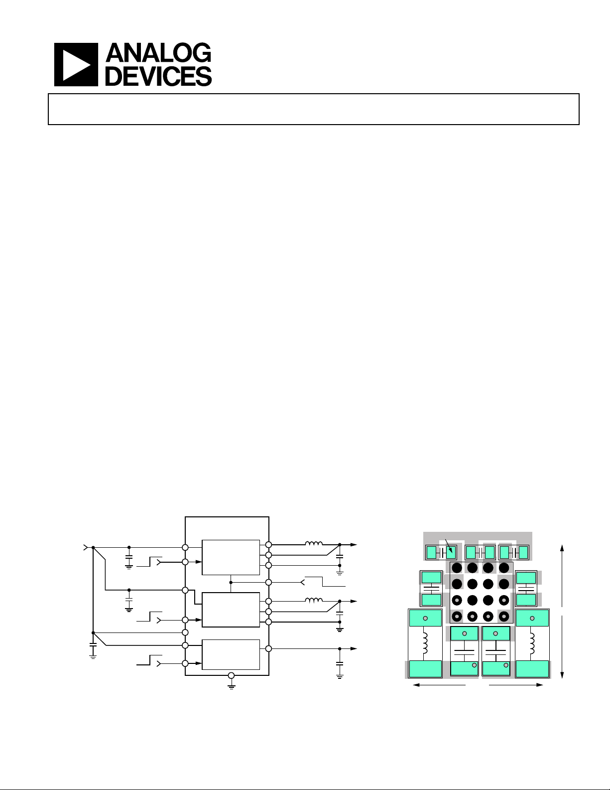
ADP5022
VIN = 2.4V
TO 5.5V
1µF
VIN1
OFF
OFF
OFF
ON
ON
ON
EN1
VIN2
EN2
VDDA
VIN3
EN3
C2
4.7µF
C3
4.7µF
C1
BUCK1
EN_BK1
MODE
MODE
BUCK2
EN_BK2
LDO1
EN_LDO1
AGND
SW1
VOUT1
PGND1
MODE
SW2
VOUT2
PGND2
VOUT3
Figure 1. Typical Applications Circuit Figure 2. Typical PCB Layout
Rev. B
Information furnished by Analog Devices is believed to be accurate and reliable. However, no
responsibility is assumed by Analog Devices for its use, nor for any infringements of patents or other
rights of third parties that may result from its use. Specifications subject to change without notice. No
license is granted by implication or otherwise under any patent or patent rights of Analog Devices.
Trademarks and registered trademarks are the property of their respective owners.
L1
1µH
PWM
L2
1µH
PWM/PSM
V
@
OUT1
600mA
C4
10µF
V
@
OUT2
600mA
C5
10µF
V
@
OUT3
150mA
C6
1µF
08253-001
One Technology Way, P.O. Box 9106, Norwood, MA 02062-9106, U.S.A.
Tel: 781.329.4700 www.analog.com
Fax: 781.461.3113 ©2009–2010 Analog Devices, Inc. All rights reserved.
C1
L1
COUT_3
C4C3
INDUCTOR
COUT_1 COUT_2
4.7mm
C2
5.0mm
INDUCTOR
08253-061
Page 2

ADP5022
TABLE OF CONTENTS
Features .............................................................................................. 1
Applications ....................................................................................... 1
General Description ......................................................................... 1
Revision History ............................................................................... 2
Specifications ..................................................................................... 3
Buck1 and Buck2 Specifications ................................................. 4
LDO Specifications ...................................................................... 5
Absolute Maximum Ratings ............................................................ 6
Thermal Data ................................................................................ 6
Thermal Resistance ...................................................................... 6
ESD Caution .................................................................................. 6
Pin Configuration and Function Descriptions ............................. 7
Typical Performance Characteristics ............................................. 8
REVISION HISTORY
6/10—Rev. A to Rev. B
Changes to Ordering Guide .......................................................... 25
11/09—Revision A: Initial Version
Theory of Operation ...................................................................... 16
Power Management Unit ........................................................... 16
Buck Section ................................................................................ 17
LDO Section ............................................................................... 18
Applications Information .............................................................. 19
Buck External Component Selection ....................................... 19
LDO Capacitor Selection .......................................................... 20
PCB Layout Guidelines .................................................................. 22
Evaluation Board schematics and Artwork ................................ 23
Suggested Layout ........................................................................ 23
Outline Dimensions ....................................................................... 25
Ordering Guide .......................................................................... 25
Rev. B | Page 2 of 28
Page 3

ADP5022
SPECIFICATIONS
VDDA = VIN1 = VIN2 = 3.6 V, VIN3 = (VOUT3 + 0.5 V) or 2.4 V, whichever is greater, VIN3 ≤ VIN1, TJ = −40°C to +125°C, unless
otherwise noted.
Table 1.
Parameter Symbol Test Conditions/Comments Min Typ Max Unit
INPUT VOLTAGE RANGE
System and Buck Input Supplies Voltage Range
High UVLO level models 4.5 5.5 V
LDO Input Supply Voltage Range V
SHUTDOWN CURRENT
I
THERMAL SHUTDOWN
Thermal Shutdown Threshold TSDTH T
Thermal Shutdown Hysteresis TSD
EN1, EN2, EN3, MODE INPUTS
EN1, EN2, EN3, MODE Input Logic High VIH VDDA = VIN1 = VIN2 1.2 V
EN1, EN2, EN3, MODE Input Logic Low VIL VDDA = VIN1 = VIN2 0.4 V
EN1, EN2, EN3, MODE Input Leakage Current V
STANDBY CURRENT
All Channels Enabled, No Load I
All Channels Enabled, No Load, No Buck Switching I
VIN3 UNDERVOLTAGE LOCKOUT
Input Voltage Rising UVLO
Input Voltage Falling UVLO
VDDA UNDERVOLTAGE LOCKOUT
Input Voltage Rising UVLO
Low UVLO level (factory programmed) 2.35 V
Input Voltage Falling UVLO
Low UVLO level (factory programmed) 2.00 V
1
All limits at temperature extremes are guaranteed via correlation using standard statistical quality control.
1
, V
V
DDA
IN1
and V
IN2
2.3 5.5 V
IN3
EN1 = EN2 = EN3 = GND 0.5 µA
GND-SD
20 °C
HYS
Pin at (VDDA = VIN1 = VIN2) or GND 0.05 1 µA
I-LEAKAGE
80 µA
STBY
59 85 µA
STBY-NOSW
VIN3RISE
VIN3FALL
VDDARISE
VDDAFALL
Low UVLO level models 2.4 5.5 V
,
EN1 = EN2 = EN3 = GND
= −40°C to +85°C
T
J
rising 150 °C
J
2 µA
2.20 V
1.45 V
High UVLO level (factory programmed) 4.15 V
High UVLO level (factory programmed) 3.40 V
Rev. B | Page 3 of 28
Page 4

ADP5022
BUCK1 AND BUCK2 SPECIFICATIONS
VDDA = VIN1 = VIN2 = 3.6 V, VIN3 = (VOUT3 + 0.5 V) or 2.4 V, whichever is greater, VIN3 ≤ VIN1, TJ = −40°C to +125°C, unless
otherwise noted.
Table 2.
Parameter Symbol Test Conditions/Comments Min Typ Max Unit
OPERATING SUPPLY CURRENT
Buck1 Only I
Buck2 Only I
Buck1 and Buck2 Only I
OUTPUT VOLTAGE ACCURACY V
POWER SAVE MODE TO PWM CURRENT
THRESHOLD
PWM TO POWER SAVE MODE CURRENT
THRESHOLD
SW CHARACTERISTICS, BUCK1 and BUCK2
PFET On Resistance R
Typical at VIN1 = VIN2 = 5.0 V 125 mΩ
NFET On Resistance R
Typical at VIN1 = VIN2 = 5.0 V 100 mΩ
Current Limit I
OSCILLATOR FREQUENCY FSW 2.5 3.0 3.5 MHz
START-UP TIME2
From Shutdown State T
1
All limits at temperature extremes are guaranteed via correlation using standard statistical quality control.
2
Start-up time is defined as the time from a rising edge on EN1/EN2 to VOUT1/VOUT2 reaching 90% of their nominal value.
1
GND1
= 0 mA, device not switching, EN1
I
LOAD 1
24 A
= VDDA, EN2 = EN3 = GND
GND2
= 0 mA, device not switching, EN2
I
LOAD 2
32 A
= VDDA, EN1 = EN3 = GND
GND1-2
I
LOAD 1
= I
= 0 mA, device not switch-
LOAD 1
48 64 A
ing, EN1 = EN2 = VDDA, EN3 = GND
, V
OUT1
I
PSM-PWM
I
PWM-PSM
PFET
NFET
LIMIT1
STARTUP12-SD
OUT2
PWM mode, VIN1 = VIN2 = 2.4 V to 5.5 V,
= I
I
LOAD 1
= 0 mA − 600 mA
LOAD 2
−3 +3 %
105 mA
100 mA
Typical at VIN1 = VIN2 = 3.6 V 165 275 mΩ
Typical at VIN1 = VIN2 = 3.6 V 125 220 mΩ
, I
PFET switch peak current limit 750 950 1050 mA
LIMIT2
250 s
Rev. B | Page 4 of 28
Page 5
ADP5022
LDO SPECIFICATIONS
VDDA = VIN1 = VIN2 = 3.6 V, VIN3 = (VOUT3 + 0.5 V) or 2.3 V, whichever is greater, VIN3 ≤ VIN1, I
1 µF, T
= −40°C to +125°C, unless otherwise noted.1
J
Table 3.
Parameter Symbol Test Conditions/Comments Min Typ Max Unit
OPERATING SUPPLY CURRENT2 I
I
I
I
OUTPUT VOLTAGE ACCURACY V
VIN3-GND
= 0 µA 11 21 µA
OUT3
= 10 mA 16 29 µA
OUT3
= 150 mA 31 43 µA
OUT3
OUT3
100 µA < I
< 150 mA,
OUT3
VIN3 = (VOUT3 + 0.5 V) to 5.5 V
REGULATION
Line Regulation VOUT3/V
Load Regulation3 VOUT3/I
VIN3 = (VOUT3 + 0.5 V) to 5.5 V, I
IN3
I
OUT3
= 1 mA to 150 mA 0.002 0.0075 %/mA
OUT3
= 1 mA −0.03 +0.03 %/ V
OUT
DROPOUT VOLTAGE4
V
VOUT3 = 3.0 V, I
VOUT3 = 3.0 V, I
DROPOUT
= 10 mA 7 mV
OUT3
= 150 mA 110 150 mV
OUT3
START-UP TIME5
From Shutdown State T
CURRENT-LIMIT THRESHOLD6 I
STARTUP3-SD
LIMIT3
OUTPUT NOISE OUT
200 µs
160 240 350 mA
NOISE
10 Hz to 100 kHz, VIN3 = 5 V, VOUT3 = 3.3 V 65 µV rms
10 Hz to 100 kHz, VIN3= 5 V, VOUT3 = 2.4 V 52 µV rms
10 Hz to 100 kHz, VIN3 = 5 V, VOUT3 = 1.2 V 40 µV rms
POWER SUPPLY REJECTION RATIO PSRR
10 kHz, VIN3 = 5 V, VOUT3 = 3.3 V 60 dB
10 kHz, VIN3 = 5 V, VOUT3 = 2.3 V 66 dB
10 kHz, VIN3 = 5 V, VOUT3 = 1.2 V 70 dB
1
All limits at temperature extremes are guaranteed via correlation using standard statistical quality control.
2
LDO operating supply current is the current drawn from VIN3 to AGND when the LDO is enabled. Whenever any regulator channel is enabled, current is drawn from
VIN1 to AGND. This current is 8 µA typical and is included in the I
3
Based on an end-point calculation using 1 mA and 150 mA loads.
4
Dropout voltage is defined as the input-to-output voltage differential when the input voltage is set to the nominal output voltage. This applies only for output
voltages above 2.3 V.
5
Start-up time is defined as the time between the rising edge of EN3 to VOUT3 being at 90% of its nominal value.
6
Current-limit threshold is defined as the current at which VOUT3 drops to 90% of the specified typical value. For example, the current limit for a 3.0 V output voltage is
defined as the current that causes the output voltage to drop to 90% of 3.0 V or 2.7 V.
GND1
, I
GND2
, and I
specifications.
GND1-2
= 10 mA; C
OUT3
IN3
= C
OUT3
=
−2 +2 %
Rev. B | Page 5 of 28
Page 6
ADP5022
ABSOLUTE MAXIMUM RATINGS
of the package is based on modeling and calculation using a
θ
Table 4.
Parameter Rating
VDDA, VIN1, VIN2, VIN3, VOUT1, VOUT2,
VOUT3, EN1, EN2, EN3, MODE to GND
Storage Temperature Range −65°C to +150°C
Operating Junction Temperature Range −40°C to +125°C
Soldering Conditions JEDEC J-STD-020
−0.3 V to +6 V
Stresses above those listed under Absolute Maximum Ratings
may cause permanent damage to the device. This is a stress
rating only; functional operation of the device at these or any
other conditions above those indicated in the operational
section of this specification is not implied. Exposure to absolute
maximum rating conditions for extended periods may affect
device reliability.
THERMAL DATA
Absolute maximum ratings apply individually only, not in
combination.
The ADP5022 can be damaged when the junction temperature
limits are exceeded. Monitoring ambient temperature (T
not guarantee that the junction temperature (T
) is within the
J
specified temperature limits. In applications with high power
dissipation and poor thermal resistance, the maximum ambient
temperature may have to be derated. In applications with
moderate power dissipation and low PCB thermal resistance,
the maximum ambient temperature may exceed the maximum
limit as long as the junction temperature is within specification
limits. T
dissipation (P
thermal resistance (θ
calculated from T
of the device is dependent on TA, the power
J
) of the device, and the junction-to-ambient
D
) of the package. Maximum TJ is
JA
and PD using the following formula:
A
= TA + (PD × θJA)
T
J
) does
A
JA
4-layer board. The junction-to-ambient thermal resistance is
highly dependent on the application and board layout. In
applications where high maximum power dissipation exists,
close attention to thermal board design is required. The value
of θ
may vary, depending on PCB material, layout, and envi-
JA
ronmental conditions. The specified values of θ
are based on a
JA
4-layer, 4” × 3” circuit board. Refer to JEDEC JESD 51-9 for
detailed information on the board construction. For additional
information, see the AN-617 Application Note, MicroCSP
TM
Wafer L ev e l Chi p Scal e Pa ck ag e.
THERMAL RESISTANCE
θJA is specified for the worst-case conditions, that is, a device
soldered on a circuit board.
Table 5. Thermal Resistance
Package Type θJA Unit
16-Ball, 0.5 mm Pitch WLCSP 65 °C/W
ESD CAUTION
Rev. B | Page 6 of 28
Page 7
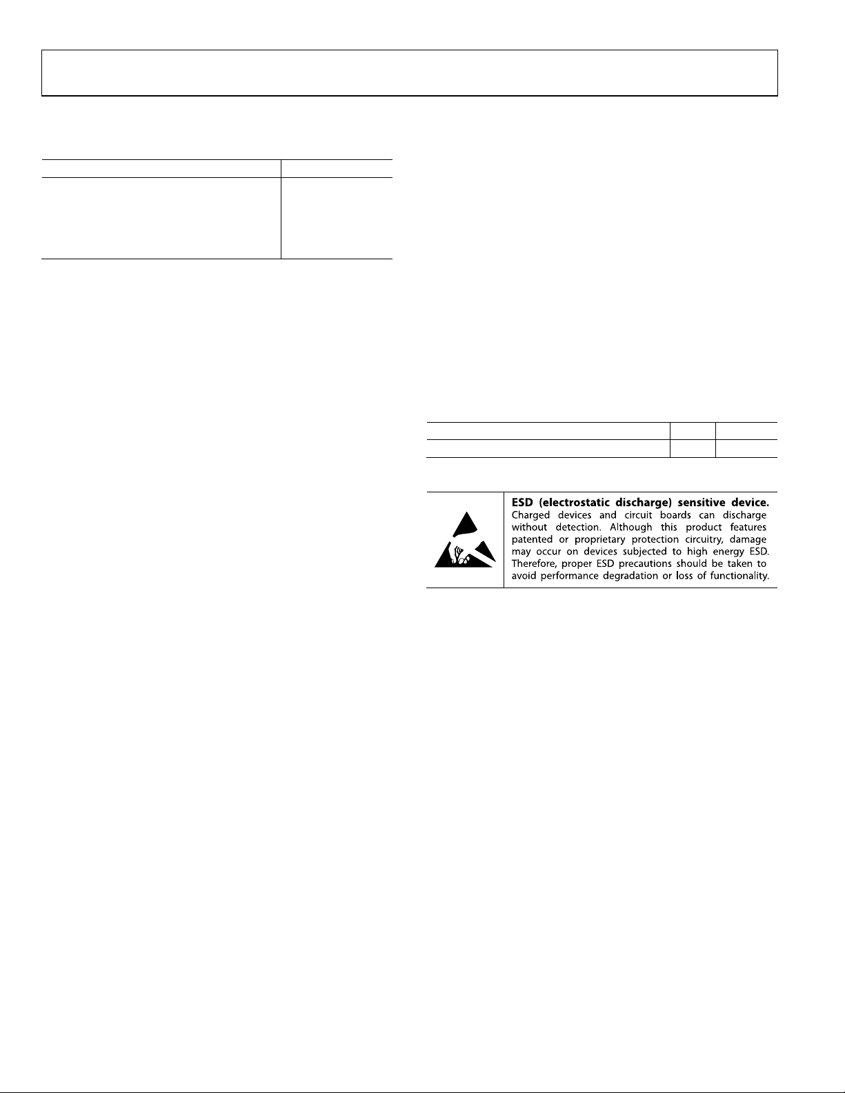
ADP5022
PIN CONFIGURATION AND FUNCTION DESCRIPTIONS
BALLA1
INDICATOR
VOUT3
A
B
C
PGND1
D
Figure 3. Pin Configuration
Table 6. Pin Function Descriptions
Pin No. Mnemonic Description
A1 VOUT3 LDO Output Voltage and Sensing Input.
A2 AGND Analog Ground.
A3 VIN3 LDO Input Supply (VIN3 ≤ VIN1 = VIN2 = VDDA).
A4 VDDA Supply Input for the Housekeeping Block and UVLO Sensing.
B1 VIN1 Buck1 Input Supply (VIN1 = VIN2 = VDDA).
B2 EN1 Buck1 Activation. Set EN1 = high: turn on Buck1. Set EN1 = low: turn off Buck1.
B3 EN2 Buck2 Activation. Set EN2 = high: turn on Buck2. Set EN2 = low: turn off Buck2.
B4 VIN2 Buck2 Input Supply (VIN2 = VIN1 = VDDA).
C1 SW1 Buck1 Switching Node.
C2 EN3 LDO Activation. Set EN3 = high: turn on LDO. EN3 = low: turn off LDO.
C3 MODE Buck1/Buck2 Operating Mode: MODE = high: forced PWM operation. MODE = low: auto PWM/PSM operation.
C4 SW2 Buck2 Switching Node.
D1 PGND1 Dedicated Power Ground for Buck1.
D2 VOUT1 Buck1 Output Voltage Sensing Input.
D3 VOUT2 Buck2 Output Voltage Sensing Input.
D4 PGND2 Dedicated Power Ground for Buck2.
234
1
AGND
VIN1
EN1
SW1
EN3
VOUT1
TOP VIEW
(BALL SIDE DOW N)
Not to Scal e
VIN3
EN2
MODE
VOUT2
VDDA
VIN2
SW2
PGND2
08253-002
Rev. B | Page 7 of 28
Page 8
ADP5022
TYPICAL PERFORMANCE CHARACTERISTICS
VIN1 = VIN2 = VIN3 = VDDA = 5.0 V, TA = 25°C, unless otherwise noted.
T
1
2
VOUT1
VOUT2
VOUT3
3
CH1 2.00V M 200µ s A CH1 1.92V
CH3 2.00V
B
W
B
W
CH2 2.00V
B
W
T 45.40%
08253-023
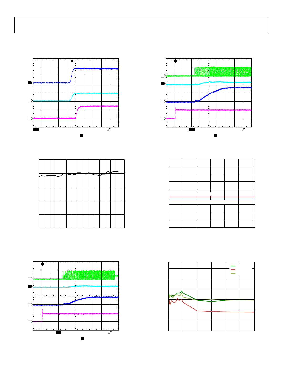
Figure 4. 3-Channel Start-Up Waveforms, VIN3 Cascaded from VOUT1
0.00010
0.00008
0.00006
A (A)
IN
I
0.00004
0.00002
0
2.82.62.4 3.0 3.2 3.4 3.6 3.8 4.0 4.2 4.4 4.6 4.8 5.0 5.2 5.4
(V)
V
IN
Figure 5. System Quiescent Current vs. Input Voltage, VOUT1 = 0.8 V,
VOUT2 = 2.5 V, VIN3 = VOUT2, VOUT3 = 1.2 V, All Channels Unloaded
T
4
2
1
3
CH1 2.00V
CH3 5.00V
SW
VOUT
EN
I
IN
B
CH2 50.0mA Ω
W
B
CH4 5.00V
W
B
M 40.0µs A CH3 2. 2V
W
B
W
T 11.20%
Figure 7. Buck2 Startup, VOUT2 = 1.8 V, I
OUT2
08253-020
= 5 mA
0.15
0.14
0.13
0.12
0.11
0.10
0.09
OUTPUT CURRENT (A)
PSM TO PWM
PWM TO PSM
0.08
0.07
0.06
2.4 2. 9 3. 4 3. 9 4. 4 4.9 5.4
08253-064
INPUT VOLTAGE (V)
08253-067
Figure 8. Buck 2 PSM to PWM Transition, VOUT2 = 1.8 V
T
4
2
1
3
CH1 2.00V
CH3 5.00V
SW
VOUT
EN
I
IN
B
B
W
W
CH2 50.0mA Ω
CH4 5.00V
B
W
B
W
Figure 6. Buck1 Startup, VOUT1 = 3.3 V, I
M 40.0µs A CH3 2.2V
T 11.20%
= 10 mA
OUT1
08253-021
Rev. B | Page 8 of 28
3.354
TA= +25°C
T
= –40°C
A
T
= +85°C
A
3.334
3.314
A (V)
3.294
OUT
V
3.274
3.254
3.234
0 0.1 0.2 0.3 0.4 0.6
I
(A)
OUT
0.5
Figure 9. Buck1 Load Regulation Across Temperature, VOUT1 = 3.3 V,
Auto Mode
08253-058
Page 9
ADP5022
1.834
1.824
1.814
1.804
B (V)
OUT
1.794
V
1.784
1.774
1.764
0 0.1 0.2 0.3 0.4 0.6
I
OUT
(A)
TA= +25°C
T
= –40°C
A
T
= +85°C
A
0.5
Figure 10. Buck2 Load Regulation Across Temperature, VOUT2 = 1.8 V,
Auto Mode
08253-057
100
90
80
70
(A)
VIN = 3.6V
V
= 4.5V
IN
V
= 5.5V
IN
60
50
40
EFFICIENCY (%)
30
20
10
0
0.0001 0.001 0.01 0.1 1
I
OUT
Figure 13. Buck1 Efficiency vs. Load Current, Across Input Voltage,
VOUT1 = 3.3 V, Auto Mode
08253-038
1.834
1.824
1.814
1.804
B (V)
OUT
V
1.794
1.784
1.774
1.764
0 0.1 0.2 0.3 0.4 0.60.5
I
OUT
(A)
VIN = 5.5V
V
= 4.5V
IN
V
= 3.6V
IN
V
= 2.4V
IN
Figure 11. Buck 2 Load Regulation Across Input Voltage, VOUT1 = 1.8 V,
PWM Mode
3.354
3.334
3.314
A (V)
3.294
OUT
V
3.274
3.254
3.234
0 0.1 0.2 0.3 0.4 0.60.5
I
OUT
(A)
VIN = 3.6V
V
= 4.5V
IN
V
= 5.5V
IN
Figure 12. Buck1 Load Regulation Across Input Voltage, VOUT2 = 3.3 V,
PWM Mode
100
90
80
70
60
50
40
EFFICIENCY (%)
30
20
10
0
08253-054
0.001 0.01 0. 1 1
I
OUT
(A)
VIN = 3.6V
V
= 4.5V
IN
V
= 5.5V
IN
08253-039
Figure 14. Buck1 Efficiency vs. Load Current, Across Input Voltage,
VOUT1 = 3.3 V, PWM Mode
100
90
80
70
60
50
40
EFFICIENCY (%)
30
20
10
0
08253-055
0.0001 0.001 0.01 0.1 1
I
OUT
(A)
VIN = 5.5V
V
= 4.5V
IN
V
= 3.6V
IN
V
= 2.4V
IN
08253-036
Figure 15. Buck2 Efficiency vs. Load Current, Across Input Voltage,
VOUT2 = 1.8 V, Auto Mode
Rev. B | Page 9 of 28
Page 10

ADP5022
100
90
80
70
60
50
40
EFFICIENCY (%)
30
20
10
0
0.001 0.01 0. 1 1
I
OUT
(A)
VIN = 5.5V
V
= 4.5V
IN
V
= 3.6V
IN
V
= 2.4V
IN
Figure 16. Buck2 Efficiency vs. Load Current, Across Input Voltage,
VOUT2 = 1.8 V, PWM Mode
100
90
80
70
60
50
40
EFFICIENCY (%)
30
20
10
0
0.0001 0.001 0.01 0. 1 1
I
OUT
(A)
VIN = 2.4V
V
= 3.6V
IN
V
= 4.5V
IN
V
= 5.5V
IN
Figure 17. Buck1 Efficiency vs. Load Current, Across Input Voltage,
VOUT1 = 0.8 V, Auto Mode
08253-035
08253-034
100
90
80
70
60
50
40
EFFICIENCY (%)
30
20
10
0
0.0001 0.001 0.01 0.1 1
I
OUT
(A)
TA= –40°C
T
= +25°C
A
T
= +85°C
A
Figure 19. Buck1 Efficiency vs. Load Current, Across Temperature,
VOUT1 = 3.3 V, Auto Mode
100
90
80
70
60
50
40
EFFICIENCY (%)
30
20
10
0
0.0001 0.001 0.01 0.1 1
I
OUT
(A)
TA= +25°C
T
= –40°C
A
T
= +85°C
A
Figure 20. Buck2 Efficiency vs. Load Current, Across Temperature,
VOUT2 = 1.8 V, Auto Mode
08253-062
08253-063
100
90
80
70
60
50
40
EFFICIENCY (%)
30
20
10
0
0.001 0.01 0. 1 1
I
OUT
(A)
VIN = 2.4V
V
= 3.6V
IN
V
= 4.5V
IN
V
= 5.5V
IN
Figure 18. Buck1 Efficiency vs. Load Current, Across Input Voltage,
VOUT1 = 0.8 V, PWM Mode
08253-065
Rev. B | Page 10 of 28
3.5
3.4
3.3
3.2
3.1
3.0
2.9
FREQUENCY (MHz)
2.8
2.7
2.6
2.5
0 0.1 0.2 0.3 0.4 0.60.5
OUTPUT CURRENT (A)
TA= +25°C
T
= –40°C
A
T
= +85°C
A
Figure 21. Buck2 Switching Frequency vs. Output Current, Across
Temperature, VOUT2 = 1.8 V, PWM Mode
08253-040
Page 11

ADP5022
T
VOUT
1
1
T
VOUT
I
SW
2
SW
4
CH1 50.0V M 4. 00µs A CH2 240mA
Figure 22. Typical Waveforms, VOUT1 = 3.3 V, I
B
CH2 500mA Ω
W
CH4 2.00V
B
W
T 28.40%
OUT1
T
VOUT
1
I
2
SW
SW
4
CH1 50.0V M 4. 00µs A CH2 220mA
Figure 23. Typical Waveforms, VOUT2 = 1.8 V, I
B
CH2 500mA Ω
W
CH4 2.00V
B
W
T 28.40%
OUT2
08253-025
= 30 mA, Auto Mode
08253-024
= 30 mA, Auto Mode
I
SW
2
SW
4
CH1 50mV M 400ns A CH2 220mA
Figure 25. Typical Waveforms, VOUT2 = 1.8 V, I
B
CH2 500mA Ω
W
CH4 2.00V
B
W
T 28.40%
= 30 mA, PWM Mode
OUT2
08253-026
T
VIN
1
VOUT
SW
3
CH1 50.0mV
CH3 1.00V CH4 2.00V
B
W
B
W
M 1.00ms A CH3 4.80V
B
W
T 30.40%
08253-012
Figure 26. Buck1 Response to Line Transient, Input Voltage from 4.5 V to
5.0 V, VOUT1 = 3.3 V, PWM Mode
T
VOUT
1
I
SW
2
SW
4
CH1 50mV M 400ns A CH2 220mA
Figure 24. Typical Waveforms, VOUT1 = 3.3 V, I
B
CH2 500mA Ω
W
CH4 2.00V
B
W
T 28.40%
OUT1
08253-027
= 30 mA, PWM Mode
Rev. B | Page 11 of 28
T
VIN
1
VOUT
SW
4
3
CH1 50.0mV
CH3 1.00V CH4 2.00V
B
W
B
W
M 1.00ms A CH3 4.80V
B
W
T 30.40%
Figure 27. Buck2 Response to Line Transient, VIN = 4.5 V to 5.0 V,
VOUT2 = 1.8 V, PWM Mode
08253-013
Page 12

ADP5022
T
SW
4
VOUT
1
I
OUT
2
CH1 50.0mV
B
CH2 50.0mA Ω
W
CH4 5.00V
B
M 20.0µs A CH2 356mA
W
B
T 60.000µs
W
Figure 28. Buck1 Response to Load Transient, I
VOUT1 = 3.3 V, Auto Mode
T
SW
4
VOUT
1
from 1 mA to 50 mA,
OUT1
T
SW
4
B
CH2 200mA Ω
W
CH4 5.00V
VOUT
I
OUT
B
M 20.0µs A CH2 88.0mA
W
B
W
T 19.20%
from 20 mA to 180 mA,
OUT2
08253-018
1
2
CH1 100mV
08253-016
Figure 31. Buck2 Response to Load Transient, I
VOUT2 = 1.8 V, Auto Mode
T
VOUT2
2
3
SW1
VOUT1
I
OUT
2
CH1 50.0mV
B
CH2 50.0mA Ω
W
CH4 5.00V
B
M 20.0µs A CH2 379mA
W
B
W
T 22.20%
Figure 29. Buck2 Response to Load Transient, I
VOUT2 = 1.8 V, Auto Mode
T
SW
4
VOUT
1
I
OUT
2
CH1 50.0mV
B
CH2 200mA Ω
W
CH4 5.00V
B
M 20.0µs A CH2 408mA
W
B
W
T 20.40%
Figure 30. Buck1 Response to Load Transient, I
VOUT1 = 3.3 V, Auto Mode
from 1 mA to 50 mA,
OUT2
from 20 mA to 180 mA,
OUT1
1
4
08253-015
CH1 5.00V
CH3 5.00V
SW2
B
W
B
W
CH2 5.00V
CH4 5.00V
B
M 400ns A CH4 1. 90V
W
B
W
T 50.00%
08253-066
Figure 32. VOUT and SW Waveforms for Buck1 and Buck2 in PWM Mode
Showing Out-of-Phase Operation
T
I
2
1
IN
VOUT
EN
3
CH1 2.00V M 40.0µs A CH3 2.2V
08253-017
CH3 5.00V
B
CH2 50.0mA Ω
W
B
W
Figure 33. LDO Startup, VOUT3 = 3.0 V, I
B
W
B
W
T 11.20%
OUT3
08253-022
= 5 mA
Rev. B | Page 12 of 28
Page 13

ADP5022
2.820
2.815
2.810
2.805
C (V)
2.800
OUT
V
2.795
2.790
2.785
2.780
VIN = 3.3V
= 4.5V
V
IN
= 5.0V
V
IN
= 5.5V
V
IN
0 0.02 0.04 0. 06 0.08 0. 10 0.12 0. 14
I
OUT
(A)
Figure 34. LDO Load Regulation Across Input Voltage, VOUT3 = 2.8 V
08253-046
50
45
40
35
30
25
20
15
GROUND CURRENT (µA)
10
5
0
3.3 3 .8 4.3 4.8 5.3
INPUT VOLTAGE (V)
150mA
100mA
10mA
1mA
100µA
1µA
08253-043
Figure 37. LDO Ground Current vs. Input Voltage, Across Output Load,
VOUT3 = 2.8 V
2.85
2.84
2.83
2.82
2.81
C (V)
2.80
OUT
V
2.79
2.78
2.77
2.76
2.75
0 0.02 0.04 0.06 0.08 0.10 0.12 0.14 0.16
I
OUT
(A)
TA = –40°C
T
= +25°C
A
T
= +85°C
A
08253-049
Figure 35. LDO Load Regulation Across Temperature, VIN3 = 3.3 V, VOUT3 = 2.8 V
3.0
2.5
2.0
C (V)
1.5
OUT
V
1.0
0.5
I
OUT
I
OUT
I
OUT
I
OUT
I
OUT
= 150mA
= 100mA
= 10mA
= 1mA
= 100µA
50
45
40
35
30
25
20
15
GROUND CURRENT (µA)
10
5
0
0 0.02 0.04 0.06 0.08 0.10 0.12 0.14
LOAD CURRENT (A)
08253-044
Figure 38. LDO Ground Current vs. Output Load, VIN3 = 3.3 V, VOUT3 = 2.8 V
3.0
2.5
2.0
A (V)
1.5
OUT
V
1.0
VIN = 3.6V
= 4.5V
V
0.5
V
IN
= 5.5V
IN
0
2.4 2.6 2.8 3.0 3.2 3.4 3. 6 3.8 4.0 4.2 4. 4 4.6 4.8 5.0 5.2 5.4
(V)
V
IN
Figure 36. LDO Line Regulation Across Output Load, VOUT3 = 2.8 V
08253-045
Rev. B | Page 13 of 28
0
0 0.05 0.10 0.15 0.20 0.25 0.30 0. 35 0. 40
I
OUT
(A)
Figure 39. LDO Current Capability Across Input Voltage, VOUT3 = 2.8 V
08253-030
Page 14

ADP5022
T
I
OUT
2
1
VOUT
65
60
55
50
45
40
RMS NOISE (µ V)
35
30
5VIN
3.3VIN
CH1 100mV M 40.0µs A CH2 52. 0mA
B
CH2 100mA Ω
W
Figure 40. LDO Response to Load Transient, I
B
W
T 19.20%
from 1 mA to 80 mA,
OUT3
08253-019
VOUT3 = 2.8 V
T
VIN
2
1
3
VOUT
CH1 20.0mV
CH3 1.00V
B
W
B
W
M 100µs A CH3 4.80V
T 28.40%
08253-014
Figure 41. LDO Response to Line Transient, Input Voltage from 4.5 V to 5.5 V,
VOUT3 = 2.8 V
60
55
50
45
40
RMS NOISE (µV)
35
30
25
0.001 0.01 0.1 1 10 100
5VIN
3.3VIN
I
LOAD
(mA)
08253-047
Figure 42. LDO Output Noise vs. Load Current, Across Input Voltage,
VOUT3 = 2.8 V
25
0.001 0.01 0.1 1 1 0 100
I
LOAD
(mA)
08253-048
Figure 43. LDO Output Noise vs. Load Current, Across Input Voltage,
VOUT3 = 3.0 V
0
100µA
–10
1mA
10mA
–20
50mA
100mA
–30
150mA
–40
–50
PSRR (dB)
–60
–70
–80
–90
–100
10 100 1k 10k 100k 1M 10M
FREQUENCY (Hz)
Figure 44. LDO PSRR Across Output Load, VIN3 = 3.3 V, VOUT3 = 2.8 V
0
–20
–40
–60
PSRR (dB)
–80
–100
–120
10 100 1k 10k 100k 1M 10M
FREQUENCY (Hz)
100µA
1mA
10mA
50mA
100mA
150mA
Figure 45. LDO PSRR Across Output Load, VIN3 = 3.3 V, VOUT3 = 3.0 V
08253-050
08253-051
Rev. B | Page 14 of 28
Page 15

ADP5022
0
100µA
–20
–40
–60
PSRR (dB)
–80
–100
–120
10 100 1k 10k 100k 1M 10M
1mA
10mA
50mA
100mA
150mA
FREQUENCY (Hz)
Figure 46. LDO PSRR Across Output Load, VIN3 = 5.0 V, VOUT3 = 2.8 V
08253-053
0
100µA
1mA
10mA
50mA
100mA
150mA
10 100 1k 10k 100k 1M 10M
FREQUENCY (Hz)
PSRR (dB)
–100
–10
–20
–30
–40
–50
–60
–70
–80
–90
Figure 47. LDO PSRR Across Output Load, VIN3 = 5.0 V, VOUT3 = 3.0 V
08253-052
Rev. B | Page 15 of 28
Page 16

ADP5022
V
THEORY OF OPERATION
PWM
COMP
VIN1
I
LIMIT
CONTROL
SW1
PGND1
EN1
EN2
EN3
ENABLE
CONTRO L
LOW
CURRENT
DRIVER
AND
ANTISHOOT
THROUGH
GM ERROR
PWM/
PSM
BUCK1
AMP
SOFT START
PSM
COMP
LDO
UNDERVOLTAGE
LOCK OUT
LDO
CONTRO L
OUT1VOUT2
OSCILLATOR
SYSTEM
UNDERVOLTAGE
LOCK OUT
THERMAL
SHUTDOWN
R1
SOFT START
PSM
COMP
GM ERROR
AMP
PWM/
PSM
CONTROL
BUCK2
PWM
COMP
I
LIMIT
LOW
CURRENT
DRIVER
AND
ANTISHOOT
THROUGH
ADP5022
VIN2
SW2
PGND2
VDDA VIN3 AGND VOUT3 MODE
Figure 48. Functional Block Diagram
POWER MANAGEMENT UNIT
The ADP5022 is a micro power management units (micro
PMU) combining two step-down (buck) dc-to-dc converters
and a single low dropout linear regulator (LDO). The high
switching frequency and tiny 16-ball WLCSP package allow for
a small power management solution.
To combine these high performance converters and regulators
into the micro PMU, there is a system controller allowing them
to operate together.
Each regulator has a dedicated enable pin. EN1 controls the
activation for Buck1, EN2 controls the activation for Buck2,
and EN3 controls the activation of the LDO. Logic high applied to
the ENx pin turns on the regulator, and a logic low applied to
the ENx pin turns off the regulator. When a regulator is turned
on, the output voltage is controlled through a soft start circuit to
avoid a large inrush current due to the discharged output
capacitors.
R2
The buck regulators can operate in forced PWM mode if the
MODE pin is at a logic high level. In forced PWM mode, the
switching frequency of the two bucks is always constant and
does not change with the load current. If the MODE pin is at a
logic low level, the switching regulators operate in an auto
PWM/ PSM mode. In this mode, the regulators operate at fixed
PWM frequency when the load current is above the power
saving current threshold. When the load current falls below the
power saving current threshold, the regulator in question enters
power saving mode where the switching occurs in bursts. The
burst repetition is a function of the current load and the output
capacitor value. This operating mode reduces the switching
and quiescent current losses. The auto PWM/PSM mode
transition is controlled independently for each buck regulator.
The two bucks operate synchronized to each other.
08253-003
Rev. B | Page 16 of 28
Page 17

ADP5022
Thermal Protection
In the event that the junction temperature rises above 150°C,
the thermal shutdown circuit turns off the converters and the
LDO. Extreme junction temperatures can be the result of high
current operation, poor circuit board design, or high ambient
temperature. A 20°C hysteresis is included so that when thermal
shutdown occurs, the bucks and LDO do not return to operation until the on-chip temperature drops below 130°C. When
coming out of thermal shutdown, soft start is initiated.
Undervoltage Lockout
To protect against battery discharge, undervoltage lockout
(UVLO) circuitry is integrated in the system. If the input
voltage on VDDA drops below a typical 2.15 V UVLO
threshold, all channels shut down. In the buck channels,
both the power switch and the synchronous rectifier turn
off. When the voltage on VDDA rises above the UVLO
threshold, the part is enabled once more.
Alternatively, the user can select device models with a UVLO
set at a higher level, suitable for USB applications. For these
models, the device hits the turn-off threshold when the input
supply drops to 3.65 V typical.
Enable/Shutdown
When all three enable pins are held low, the device is in
shutdown mode, and the input current remains below 2 A.
BUCK SECTION
The two bucks use a fixed frequency and high speed current
mode architecture.
The bucks operate with an input voltage of 2.4 V to 5.5 V.
Control Scheme
The bucks operate with a fixed frequency, current mode PWM
control architecture at medium to high loads for high efficiency
but shift to a power save mode (PSM) control scheme at light
loads to lower the regulation power losses. When operating in
fixed frequency PWM mode, the duty cycle of the integrated
switches is adjusted and regulates the output voltage. When
operating in PSM at light loads, the output voltage is controlled
in a hysteretic manner, with higher output voltage ripple. During
part of this time, the converter is able to stop switching and
enters an idle mode, which improves conversion efficiency.
PWM Mode
In PWM mode, the bucks operate at a fixed frequency of 3 MHz
set by an internal oscillator. At the start of each oscillator cycle,
the PFET switch is turned on, sending a positive voltage across
the inductor. Current in the inductor increases until the current
sense signal crosses the peak inductor current threshold that
turns off the PFET switch and turns on the NFET synchronous
rectifier. This sends a negative voltage across the inductor,
causing the inductor current to decrease. The synchronous
rectifier stays on for the rest of the cycle. The buck regulates the
output voltage by adjusting the peak inductor current threshold.
Power Save Mode (PSM)
The bucks smoothly transition to PSM operation when the
load current decreases below the PSM current threshold. When
either of the bucks enter power save mode, an offset is induced
in the PWM regulation level, which makes the output voltage
rise. When the output voltage reaches a level approximately
1.5% above the PWM regulation level, PWM operation is
turned off. At this point, both power switches are off, and the
buck enters an idle mode. The output capacitor discharges until
the output voltage falls to the PWM regulation voltage, at which
point the device drives the inductor to make the output voltage
rise again to the upper threshold. This process is repeated while
the load current is below the PSM current threshold.
PSM Current Threshold
The PSM current threshold is set to 100 mA. The bucks employ
a scheme that enables this current to remain accurately controlled, independent of input and output voltage levels. This
scheme also ensures that there is very little hysteresis between
the PSM current threshold for entry to and exit from the PSM.
The PSM current threshold is optimized for excellent efficiency
over all load currents.
Oscillator/Phasing of Inductor Switching
The ADP5022 ensures that both bucks operate at the same
switching frequency when both bucks are in PWM mode.
Additionally, the ADP5022 ensures that when both bucks are
in PWM mode, they operate out-of-phase, whereby the Buck2
PFET starts conducting exactly half a clock period after the
Buck1 PFET starts conducting.
Rev. B | Page 17 of 28
Page 18

ADP5022
Enable/Shutdown
The bucks start operation with soft start when the EN1 or EN2
pin is toggled from logic low to logic high. Pulling the EN1 or
EN2 pin low disables that channel.
Short-Circuit Protection
The bucks include frequency foldback to prevent output current
runaway on a hard short. When the voltage at the feedback pin
falls below half the target output voltage, indicating the possibility of a hard short at the output, the switching frequency is
reduced to half the internal oscillator frequency. The reduction
in the switching frequency allows more time for the inductor to
discharge, preventing a runaway of output current.
Soft Start
The bucks have an internal soft start function that ramps the
output voltage in a controlled manner upon startup, thereby
limiting the inrush current. This prevents possible input voltage
drops when a battery or a high impedance power source is
connected to the input of the converter.
Current Limit
Each buck has protection circuitry to limit the amount of
positive current flowing through the PFET switch and the
amount of negative current flowing through the synchronous
rectifier. The positive current limit on the power switch limits
the amount of current that can flow from the input to the
output. The negative current limit prevents the inductor
current from reversing direction and flowing out of the load.
100% Duty Operation
With a drop in input voltage or with an increase in load current,
the buck may reach a limit where, even with the PFET switch
on 100% of the time, the output voltage drops below the desired
output voltage. At this limit, the buck transitions to a mode
where the PFET switch stays on 100% of the time. When the
input conditions change again and the required duty cycle
falls, the buck immediately restarts PWM regulation without
allowing overshoot on the output voltage. This is particularly
useful in battery-powered applications to achieve the longest
operation time by taking full advantage of the whole battery
voltage range. Maintaining regulation is dependent on the input
voltage, load current, and output voltage. This can be calculated
from the following equation:
V
IN(MIN)
= V
OUT(MAX)
+ I
LOAD(MAX)
× (R
DS(on)MAX
+ RL)
where:
V
is the nominal output voltage plus the maximum
OUT(MAX)
tolerance.
I
is the maximum load current plus inductor ripple
LOAD(MAX)
current.
R
R
is the maximum P-channel switch R
DS(on)MAX
is the DC resistance of the inductor.
L
DS(on)
.
LDO SECTION
The LDO is a low quiescent current, low dropout linear
regulator and provides up to 150 mA of output current.
Drawing a low 30 A quiescent current (typical) at full load
makes the LDO ideal for battery-operated portable equipment.
The LDO operates with an input voltage of 2.3 V to 5.5 V.
It also provides high power supply rejection ratio (PSRR), low
output noise, and excellent line and load transient response
with just a small 1 µF ceramic input and output capacitor.
Internally, the LDO consists of a reference, an error amplifier,
a feedback voltage divider, and a PMOS pass transistor. Output
current is delivered via the PMOS pass device, which is controlled by the error amplifier. The error amplifier compares
the reference voltage with the feedback voltage from the output
and amplifies the difference. If the feedback voltage is lower
than the reference voltage, the gate of the PMOS device is
pulled lower, allowing more current to flow and increasing
the output voltage. If the feedback voltage is higher than the
reference voltage, the gate of the PMOS device is pulled higher,
reducing the current flowing to the output.
LDO Undervoltage Lockout
The ADP5022 integrates an undervoltage lockout function
on the VIN3 input voltage, which ensures that the LDO
output drive is disabled whenever VIN3 is below a threshold
of approximately 2.0 V. Where the ADP5022 is configured to
supply VIN3 from either VOUT1 or VOUT2, this ensures that
the LDO powers up safely in this cascaded configuration.
Rev. B | Page 18 of 28
Page 19

ADP5022
APPLICATIONS INFORMATION
BUCK EXTERNAL COMPONENT SELECTION
Trade-offs between performance parameters such as efficiency
and transient response can be made by varying the choice of
external components in the applications circuit, as shown in
Figure 1.
Inductor
The high switching frequency of the ADP5022 bucks allows for
the selection of small chip inductors. For best performance, use
inductor values between 0.7 H and 3 H. Suggested inductors
are shown in Ta bl e 7 .
The peak-to-peak inductor current ripple is calculated using
the following equation:
VVV
−×
××
I
RIPPLE
OUT
LfV
2
)(
Dimensions
(mm)
I
SAT
(mA)
DCR
(mΩ)
I
RIPPLE
OUT
=
IN
IN
SW
where:
f
is the switching frequency.
SW
L is the inductor value.
The minimum dc current rating of the inductor must be greater
than the inductor peak current. The inductor peak current is
calculated using the following equation:
II +=
PEAK
)(
MAXLOAD
Inductor conduction losses are caused by the flow of current
through the inductor, which has an associated internal dc
resistance (DCR). Larger sized inductors have smaller DCR,
which may decrease inductor conduction losses. Inductor core
losses are related to the magnetic permeability of the core material.
Because the bucks are high switching frequency dc-to-dc
converters, shielded ferrite core material is recommended for
its low core losses and low EMI.
Table 7. Suggested 1.0 μH Inductors
Vendor Model
Murata LQM2MPN1R0NG0B 2.0 × 1.6 × 0.9 1400 85
Murata LQM18FN1R0M00B 1.6 × 0.8 × 0.8 150 26
Taiyo Yuden CBMF1608T1R0M 1.6 × 0.8 × 0.8 290 90
Coil craft EPL2014-102ML 2.0 × 2.0 × 1.4 900 59
TDK GLFR1608T1R0M-LR 1.6 × 0.8 × 0.8 230 80
Coilcraft 0603LS-102 1.8 × 1.69 × 1.1 400 81
Toko MDT2520-CN 2.5 × 2.0 × 1.2 1350 85
Output Capacitor
Higher output capacitor values reduce the output voltage ripple
and improve load transient response. When choosing this value,
it is also important to account for the loss of capacitance due to
output voltage dc bias.
Ceramic capacitors are manufactured with a variety of dielectrics, each with a different behavior over temperature and
applied voltage. Capacitors must have a dielectric adequate
to ensure the minimum capacitance over the necessary
temperature range and dc bias conditions. X5R or X7R
dielectrics with a voltage rating of 6.3 V or 10 V are recommended for best performance. Y5V and Z5U dielectrics are
not recommended for use with any dc-to-dc converter because
of their poor temperature and dc bias characteristics.
The worst-case capacitance accounting for capacitor variation
over temperature, component tolerance, and voltage is calculated using the following equation:
= C
C
EFF
× (1 − TEMPCO) × (1 − TOL)
OUT
where:
is the effective capacitance at the operating voltage.
C
EFF
TEMPCO is the worst-case capacitor temperature coefficient.
TOL is the worst-case component tolerance.
In this example, the worst-case temperature coefficient
(TEMPCO) over −40°C to +85°C is assumed to be 15% for an
X5R dielectric. The tolerance of the capacitor (TOL) is assumed
to be 10%, and C
is 9.2481 F at 1.8 V, as shown in Figure 49.
OUT
Substituting these values in the equation yields
= 9.2481 F × (1 − 0.15) × (1 − 0.1) = 7.0747 F
C
EFF
To guarantee the performance of the bucks, it is imperative
that the effects of dc bias, temperature, and tolerances on the
behavior of the capacitors be evaluated for each application.
12
10
8
6
4
CAPACITANCE (µF )
2
Rev. B | Page 19 of 28
0
0123456
DC BIAS VOLT AGE (V)
Figure 49. Typical Capacitor Performance
08253-004
Page 20

ADP5022
E
2
The peak-to-peak output voltage ripple for the selected output
capacitor and inductor values is calculated using the following
equation:
V
RIPPLE
SW
IN
CLf
××××
22
OUT
=
()
π
RIPPLE
SW
CfI××=8
OUT
V
Capacitors with lower equivalent series resistance (ESR) are
preferred to guarantee low output voltage ripple, as shown in
the following equation:
V
ESR ≤
COUT
RIPPLE
I
RIPPL
The effective capacitance needed for stability, which includes
temperature and dc bias effects, is a minimum of 7 µF and a
maximum of 40 µF.
Input Capacitor
Higher value input capacitors help to reduce the input voltage
ripple and improve transient response. Maximum input capacitor current is calculated using the following equation:
−
VVV
OUT
)(
IN
≥
II
CIN
OUT
MAXLOAD
)(
V
IN
To minimize supply noise, place the input capacitor as close
to the VIN pin of the BUCK as possible. As with the output
capacitor, a low ESR capacitor is recommended.
The effective capacitance needed for stability, which includes
temperature and dc bias effects, is a minimum of 3 µF and a
maximum of 10 µF. A list of suggested capacitors is shown in
Tabl e 9.
Table 8. Suggested 10 μF Capacitors
Vendor Type Model
Case
Size
Voltage
Rating (V)
Murata X5R GRM188R60J106 0603 6.3
Taiyo Yuden X5R JMK107BJ475 0603 6.3
TDK X5R C1608JB0J106K 0603 6.3
Panasonic X5R ECJ1VB0J106M 0603 6.3
The buck regulators require 10 µF output capacitors to guarantee stability and response to rapid load variations and to
transition in and out the PWM/PSM modes. In certain
applications, where one or both buck regulator powers a
processor, the operating state is known because it is controlled by software. In this condition, the processor can drive
the MODE pin according to the operating state; consequently, it
is possible to reduce the output capacitor from 10 µF to 4.7 µF
because the regulator does not expect a large load variation
when working in PSM mode, see Figure 50.
ADP5022
C2
4.7µF
V
IN
.5V TO 5.5V
ALWAYS ON
INPUTS
ACTIVATION
Figure 50. Processor System Power Management with PSM/PWM Control
VIN2
C3
4.7µF
VDDA
VIN3
C1
1µF
EN1
EN2
EN3
MICRO PMU
SW1VIN1
VOUT1
PGND1
MODE
SW2
VOUT2
PGND2
VOUT3
1µH
1µH
L1
L2
C4
4.7µF
C5
4.7µF
C6
1µF
PROCESSOR
VCORE
GPIO
VIO
ANALOG
SUB-SYSTEM
VAN A
08253-005
Table 9. Suggested 4.7 μF Capacitors
Vendor Type Model
Size
Murata X5R GRM188R60J475ME19D 0402 6.3
Taiyo Yuden X5R JMK107BJ475 0402 6.3
Panasonic X5R ECJ-0EB0J475M 0402 6.3
Case
Voltage
Rating
(V)
LDO CAPACITOR SELECTION
Output Capacitor
The ADP5022 LDO is designed for operation with small, spacesaving ceramic capacitors but functions with most commonly
used capacitors as long as care is taken with the ESR value. The
ESR of the output capacitor affects stability of the LDO control
loop. A minimum of 0.70 µF capacitance with an ESR of 1 Ω
or less is recommended to ensure stability of the ADP5022.
Transient response to changes in load current is also affected
by output capacitance. Using a larger value of output capacitance improves the transient response of the ADP5022 to large
changes in load current.
Input Bypass Capacitor
Connecting a 1 µF capacitor from VIN3 to GND reduces
the circuit sensitivity to printed circuit board (PCB) layout,
especially when long input traces or high source impedance
are encountered. If greater than 1 µF of output capacitance is
required, increase the input capacitor to match it.
Table 10. Suggested 1.0 μF Capacitors
Vendor Type Model
Size
Murata X5R GRM155B30J105K 0402 6.3
TDK X5R C1005JB0J105KT 0402 6.3
Panasonic X5R ECJ0EB0J105K 0402 6.3
Taiyo Yuden X5R LMK105BJ105MV-F 0402 10.0
Case
Voltage
Rating (V)
Rev. B | Page 20 of 28
Page 21

ADP5022
Input and Output Capacitor Properties
Use any good quality ceramic capacitors with the ADP5022
as long as they meet the minimum capacitance and maximum
ESR requirements. Ceramic capacitors are manufactured with
a variety of dielectrics, each with a different behavior over
temperature and applied voltage. Capacitors must have a
dielectric adequate to ensure the minimum capacitance over
the necessary temperature range and dc bias conditions. X5R
or X7R dielectrics with a voltage rating of 6.3 V or 10 V are
recommended for best performance. Y5V and Z5U dielectrics
are not recommended for use with any LDO because of their
poor temperature and dc bias characteristics.
Figure 51
depicts the capacitance vs. voltage bias characteristic
of a 0402 1 µF, 10 V, X5R capacitor. The voltage stability of a
capacitor is strongly influenced by the capacitor size and voltage
rating. In general, a capacitor in a larger package or higher voltage
rating exhibits better stability. The temperature variation of the
X5R dielectric is about ±15% over the −40°C to +85°C temperature range and is not a function of package or voltage rating.
1.2
1.0
Use the following equation to determine the worst-case capacitance accounting for capacitor variation over temperature,
component tolerance, and voltage.
= C
C
EFF
× (1 − TEMPCO) × (1 − TOL)
BIAS
where:
is the effective capacitance at the operating voltage.
C
BIAS
TEMPCO is the worst-case capacitor temperature coefficient.
TOL is the worst-case component tolerance.
In this example, the worst-case temperature coefficient
(TEMPCO) over −40°C to +85°C is assumed to be 15% for an
X5R dielectric. The tolerance of the capacitor (TOL) is assumed
to be 10% and C
is 0.94 F at 1.8 V as shown in Figure 51.
BIAS
Substituting these values into the following equation.
= 0.94 F × (1 − 0.15) × (1 − 0.1) = 0.719 F
C
EFF
Therefore, the capacitor chosen in this example meets the
minimum capacitance requirement of the LDO over
temperature and tolerance at the chosen output voltage.
To guarantee the performance of the ADP5022, it is imperative
that the effects of dc bias, temperature, and tolerances on the
behavior of the capacitors are evaluated for each application.
0.8
0.6
0.4
CAPACITANCE (µF)
0.2
0
012345
Figure 51. Capacitance vs. Voltage Characteristic
DC BIAS VOLT AGE (V)
6
08253-006
Rev. B | Page 21 of 28
Page 22

ADP5022
PCB LAYOUT GUIDELINES
Poor layout can affect ADP5022 performance, causing electromagnetic interference (EMI) and electromagnetic compatibility
(EMC) problems, ground bounce, and voltage losses. Poor
layout can also affect regulation and stability. A good layout is
implemented using the following guidelines:
• Place the inductor, input capacitor, and output capacitor
close to the IC using short tracks. These components carry
high switching frequencies, and large tracks act as antennas.
• Route the output voltage path away from the inductor and
SW node to minimize noise and magnetic interference.
• Maximize the size of ground metal on the component side
to help with thermal dissipation.
• Use a ground plane with several vias connecting to
the component side ground to further reduce noise
interference on sensitive circuit nodes.
Rev. B | Page 22 of 28
Page 23

ADP5022
EVALUATION BOARD SCHEMATICS AND ARTWORK
J1
J2
J3
J4
R1
0Ω
J5
J7
J6
SUGGESTED LAYOUT
C2
0603
4.7µF
C3
0603
4.7µF
C1
0402
1µF
R2
0Ω
B1
VIN1
B4
VIN2
A4
VDDA
A3
VIN3
A2
AGND
C3
MODE
B2
EN1
B3
EN2
C2
EN3
BUCK1
BUCK2
LDO
SW1
VOUT1
PGND1
SW2
VOUT2
PGND2
VOUT3
C1
D2
D1
C4
D3
D4
A1
L1
1µH
L2
1µH
C
OUT
0603
10µF
C
OUT
0603
10µF
C
OUT
0402
1µF
J8
_1
J9
J10
_2
J13
J12
_3
J11
08253-007
Figure 52. Evaluation Board Schematic
8253-008
Figure 53. Top Layer, Recommended Layout
Figure 54. Second Layer, Recommended Layout
Rev. B | Page 23 of 28
08253-009
Page 24

ADP5022
08253-010
Figure 55. Third Layer, Recommended Layout
Figure 56. Bottom Layer, Recommended Layout
08253-011
Rev. B | Page 24 of 28
Page 25

ADP5022
OUTLINE DIMENSIONS
0.660
0.602
0.544
SEATING
PLANE
0.330
0.310
0.290
1.50
REF
3
2
4
1
A
B
C
BALL 1
IDENTIFIER
2.12
2.08 SQ
2.04
0.022
REF
0.50
TOP VIEW
(BALL SIDE DOWN)
0.380
0.352
0.324
0.04 NOM
COPLANARITY
0.280
0.250
0.220
REF
BOTTOM VIEW
(BALL SIDE UP)
Figure 57. 16-Ball Wafer Level Chip Scale Package [WLCSP]
Back-Coating Included
(CB-16-7)
Dimensions shown in millimeters
ORDERING GUIDE
Output
Model1
Voltage (V)
ADP5022ACBZ-1-R7 VOUT1 = 3.3 V
Undervoltage
2
Lockout Level
Low −40°C to +125°C 16-Ball Wafer Level Chip Scale Package [WLCSP] CB-16-7 L9H
VOUT2 = 1.5 V
VOUT3 = 1.8 V
ADP5022ACBZ-2-R7 VOUT1 = 1.2 V
Low −40°C to +125°C 16-Ball Wafer Level Chip Scale Package [WLCSP] CB-16-7 L9J
VOUT2 = 1.8 V
VOUT3 = 2.8 V
ADP5022ACBZ-4-R7 VOUT1 = 3.3 V
High −40°C to +125°C 16-Ball Wafer Level Chip Scale Package [WLCSP] CB-16-7 LG7
VOUT2 = 1.8 V
VOUT3 = 3.3 V
ADP5022ACBZ-6-R7 VOUT1 = 1.0 V
Low −40°C to +125°C 16-Ball Wafer Level Chip Scale Package [WLCSP] CB-16-7 LH5
VOUT2 = 1.8 V
VOUT3 = 2.5 V
1
Z = RoHS Compliant Part.
2
For additional voltage options, contact a local sales or distribution representative. Additional output voltages and UVLO available are
Buck1 and Buck2: 3.3 V, 3.0 V, 2.8 V, 2.5 V, 2.3 V, 2.0 V, 1.82 V, 1.8 V, 1.6 V, 1.5 V, 1.3 V, 1.2 V, 1.1 V, 1.0 V, 0.9 V, 0.8 V
LDO: 3.3 V, 3.0 V, 2.9 V, 2.8 V, 2.775 V, 2.5 V, 2.0 V, 1.875 V, 1.8 V, 1.75 V, 1.7 V, 1.65 V, 1.6 V, 1.55 V, 1.5 V, 1.2 V
UVLO: 2.25 V or 3.9 V
Temperature
Range
Package Description
D
Package
Option
013009-B
Branding
Code
Rev. B | Page 25 of 28
Page 26

ADP5022
NOTES
Rev. B | Page 26 of 28
Page 27

ADP5022
NOTES
Rev. B | Page 27 of 28
Page 28

ADP5022
NOTES
©2009–2010 Analog Devices, Inc. All rights reserved. Trademarks and
registered trademarks are the property of their respective owners.
D08253-0-6/10(B)
Rev. B | Page 28 of 28
 Loading...