

Page 1
Power Management Unit
VIN2
V
V
FEATURES
Input voltage range: 2.4 V to 5.5 V
Low standby current: 1 μA
Switching frequency: 3 MHz
2
I
C interface
Synchronous Buck 1 regulator: 600 mA
Synchronous Buck 2 regulator: 250 mA
Low dropout regulator (LDO): 150 mA
Internal compensation
Internal soft start
Thermal shutdown
20-lead 4 mm × 4 mm LFCSP
APPLICATIONS
Digital cameras, handsets
Mobile TVs
for Imaging Modules
ADP5020
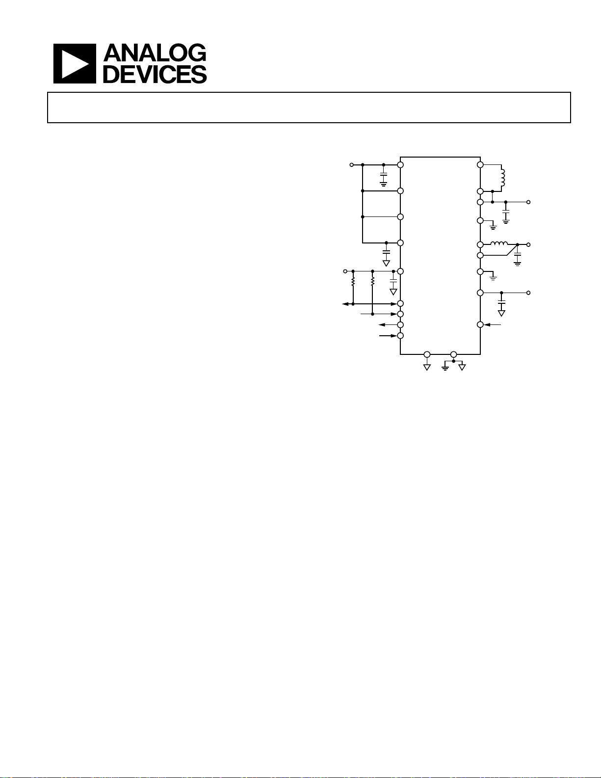
TYPICAL APPLICATIONS CIRCUIT
.4V TO 5.5
V
DD_IO
1.7V TO 3. 6
10kΩ 10kΩ
10µF
VDD1
VDD2
VDD3
ADP5020
VDDA
1µF
VDD_IO
0.1µF
SDA
SCL
XSHTDN
EN/GPIO
DGND AGND
SW1
VOUT1
VOUT1
PGND1
SW2
VOUT2
PGND2
VOUT3
SYNC
2.2µH
EXT. FREQ
9.6/19.2MHz
2.2µH
V
2.5V TO 3. 7V
10µF
V
1.1V TO 1. 8V
4.7µF
V
1.8V TO 3. 3V
1µF
OUT1
OUT2
OUT3
GENERAL DESCRIPTION
The ADP5020 provides a highly integrated power solution that
includes all of the power circuits necessary for a digital imaging
module. It comprises two step-down dc-to-dc converters, one
LDO, and a power sequence controller. All dc-to-dc converters
integrate power pMOSFETs and nMOSFETs, making the system
simpler and more compact and reducing the cost. The ADP5020
has digitally programmed output voltages and buck converters
that can source up to 600 mA. A fixed frequency operation of
3 MHz enables the use of tiny inductors and capacitors. The buck
converters use a voltage mode, constant-frequency PWM control
scheme, and the synchronous rectification is implemented to
reduce the power loss. The Buck 1 regulator operates at up to
93% efficiency.
Figure 1.
The ADP5020 provides high performance, reduces component
count and size, and is lower in cost when compared to conventional designs.
The ADP5020 runs on input voltage from 2.4 V to 5.5 V and
supports one-cell lithium-ion (Li+) batteries. The high performance LDO maximizes noise suppression. The ADP5020 can be
activated via an I
2
C® interface or through a dedicated enable input.
During logic-controlled shutdown, the input is disconnected
from the output source, and the part draws 1 μA typical from
the input source. Other key features include undervoltage lockout
to prevent deep-battery discharge and soft start to prevent input
current overshoot at startup. The ADP5020 is available in a
20-lead LFCSP.
07774-001
Rev. 0
Information furnished by Analog Devices is believed to be accurate and reliable. However, no
responsibility is assumed by Analog Devices for its use, nor for any infringements of patents or other
rights of third parties that may result from its use. Specifications subject to change without notice. No
license is granted by implication or otherwise under any patent or patent rights of Analog Devices.
Trademarks and registered trademarks are the property of their respective owners.
One Technology Way, P.O. Box 9106, Norwood, MA 02062-9106, U.S.A.
Tel: 781.329.4700 www.analog.com
Fax: 781.461.3113 ©2009 Analog Devices, Inc. All rights reserved.
Page 2

ADP5020
TABLE OF CONTENTS
Features .............................................................................................. 1
Applications ....................................................................................... 1
Typical Applications Circuit ............................................................ 1
General Description ......................................................................... 1
Revision History ............................................................................... 2
Functional Block Diagram .............................................................. 3
Specifications ..................................................................................... 4
Switching Specifications .............................................................. 5
DC-to-DC Conversion Specifications, Buck 1 Regulator ....... 5
DC-to-DC Conversion Specifications, Buck 2 Regulator ....... 6
VOUT3 Specifications, Low Dropout (LDO) Regulator ........ 6
I2C Timing Specifications ............................................................ 7
Absolute Maximum Ratings ............................................................ 8
Thermal Resistance ...................................................................... 8
ESD Caution .................................................................................. 8
Pin Configuration and Function Descriptions ............................. 9
Typical Performance Characteristics ........................................... 10
Theory of Operation ...................................................................... 13
Circuit Operation ....................................................................... 13
Internal Compensation .............................................................. 13
Current Limiting and Short-Circuit Protection ..................... 13
Synchronization .......................................................................... 13
I2C Interface ................................................................................ 13
Undervoltage Lockout ............................................................... 13
Thermal Shutdown .................................................................... 13
Control Registers ............................................................................ 14
Device Address ........................................................................... 14
Register Map ............................................................................... 14
Register Descriptions ................................................................. 14
Power-Up/Power-Down Sequence ............................................... 17
Sequencer .................................................................................... 17
Default Power-On Sequence with EN Pin .............................. 17
Power-On Sequence Using the I2C Interface .............................. 19
Power-Up/Power-Down State Flow ......................................... 20
Applications Information .............................................................. 21
Power Good Status ..................................................................... 21
XSHTDN Logic .......................................................................... 21
Components Selection ............................................................... 21
LDO Input Filter ......................................................................... 22
Layout Recommendations ............................................................. 23
Applications Schematic ............................................................. 23
PCB Board Layout Recommendations .................................... 24
External Component List .......................................................... 24
Outline Dimensions ....................................................................... 25
Ordering Guide .......................................................................... 25
REVISION HISTORY
4/09—Revision 0: Initial Version
Rev. 0 | Page 2 of 28
Page 3
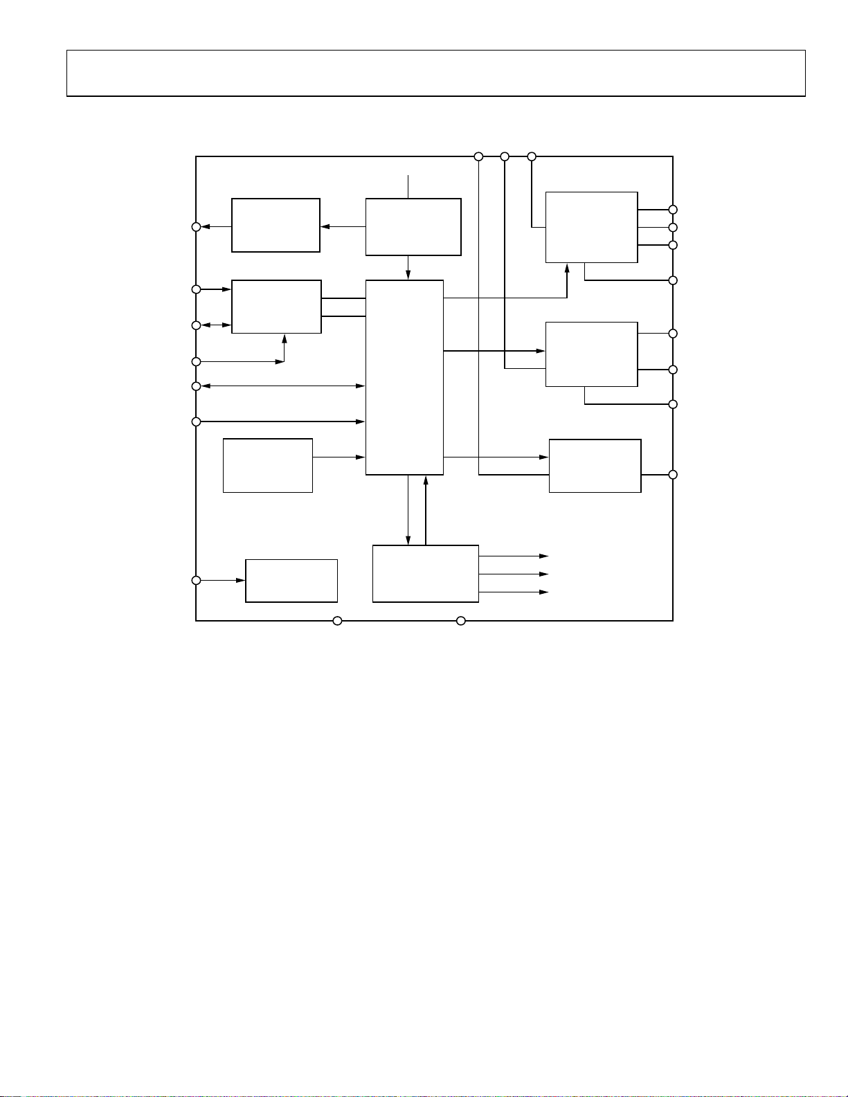
ADP5020
FUNCTIONAL BLOCK DIAGRAM
VDD3
VDD
2 VDD1
VDDA
SW1
XSHTDN
RESET
UVLO
BUCK 1
VOUT1
VOUT1
PGND1
SW2
VOUT2
PGND2
VOUT3
07774-002
VDD_IO
/
GPIO
EN
SYNC
VDDA
SCL
SDA
2
I
C
THERMAL
SHUTDOWN
HOUSE-
KEEPING
DGND
CONTROL
LOGIC
SEQUENCER
BUCK 2
LDO
BUCK1_EN
BUCK2_EN
LDO_EN
AGND
Figure 2.
Rev. 0 | Page 3 of 28
Page 4

ADP5020
SPECIFICATIONS
TJ = −40°C to +125°C, V
Table 1.
Parameter Symbol Conditions Min Typ Max Unit
OPERATING RANGE
VDDx Operating Voltage Range VDD 2.4 5.5 V
Logic I/O Operating Voltage Range
EN, SDA, SCL CHARACTERISTICS
Low Level Input Voltage VIL 0.3 × V
High Level Input Voltage VIH 0.7 × V
INPUT LOGIC CURRENT ILK Internal pull-down, 1 MΩ −1 +6 μA
XSHTDN, EN/GPIO
Low Level Output Voltage VOL I
High Level Output Voltage VOH I
OUTPUT LOGIC LEAKAGE CURRENT ILK 1 μA
UNDERVOLTAGE LOCKOUT THRESHOLD
Falling V
Rising V
POWER-ON RESET THRESHOLD
Falling V
Rising V
UVLO GLITCH DEBOUNCE TIME VDD > POR levels 50 μs
SHUTDOWN OUTPUT DURATION
POWER GOOD (POK) ACTIVATION DELAY TIME
EN to First Regulator t
First to Second Regulator t
Second to Third Regulator t
NO LOAD CURRENT CHARACTERISTICS
Standby Current I
Lockout Current I
Operating Quiescent Current, Switching
THERMAL CHARACTERISTICS
Thermal Shutdown, TJ Rising TSD
Thermal Shutdown Hysteresis
HOUSEKEEPING BLOCK
Power Good Threshold VPG
1
The V
2
Shutdown output duration is automatic when using the EN pin. To get this delay when using I2C, FORCE_XS must be set to 1.
3
Activation delays apply only when the device is activated through the EN pin or the EN_ALL bit (Address 0x03[4]); the sequencer controls the turning on of the
4
The quiescent current is calculated as though all regulators are powered up.
voltage must be less than or equal to the level on the V
DD_IO
regulators.
= 3.6 V, V
DDx
= 1.8 V, unless otherwise noted.
DD_IO
1
V
2
4
1.7 3.6 V
DD_IO
V
DD_IO
V
DD_IO
= +3 mA 0.2 × V
RST
= −3 mA 0.8 × V
RST
Referenced to V
UVLOF
Referenced to V
UVLOR
Referenced to V
PORF
Referenced to V
PORR
t
XSHTDN line driven low 1 ms
3
XSHTDN
5 ms
REG1
5 ms
REG2
5 ms
REG3
1.8 2.0 V
DDA
2.2 2.4 V
DDA
1.0 1.4 V
DDA
1.6 1.7 V
DDA
V
DD_IO
DD_IO
V
EN = 0 1 5 μA
Q(STNBY)
I
EN = 0, V
LOCK
I
Q
LOAD
supply lines.
DDx
< V
DDA
1 1 μA
UVLOF
= 0 mA 10 15 mA
150
30
°C
°C
70 80 90 %
Rev. 0 | Page 4 of 28
Page 5
ADP5020
SWITCHING SPECIFICATIONS
Table 2.
Parameter Symbol Conditions Min Typ Max Unit
SWITCHING FREQUENCY
CH1 f
CH2 f
SYNC CLOCK DIVIDER RATIO
RATIO
RATIO
SYNC CHARACTERISTICS
Frequency Range
f
f
Frequency Duty Cycle f
Signal
DC Coupling Level
Low Level Input Voltage VIL 0.3 × V
High Level Input Voltage VIH 0.7 × V
DC Coupling V
AC Coupling Level V
AC Coupling Capacitor 10 nF
Input Current I
Sync disabled 2.5 3 3.6 MHz
SW1
Sync disabled 2.5 3 3.6 MHz
SW2
SYNC_9P6 = 1 3
DIV
SYNC_19P2 = 1 6
DIV
9.6 MHz
SYNC1
19.2 MHz
SYNC2
40 50 60 %
SYNCDUTY
V
DD_IO
V
DD_IO
0 V
SYNC
Sine wave, peak-to-peak 0.5 1.0 V
CAC-PP
SYNC_9P6 = 1, or SYNC_19P2 = 1 50 μA
SYNC
V
DD_IO
V
DD_IO
DC-TO-DC CONVERSION SPECIFICATIONS, BUCK 1 REGULATOR
Table 3.
Parameter Symbol Conditions Min Typ Max Unit
OUTPUT VOLTAGE
VOUT1 REGULATION
CURRENT
POWER
SWITCH CURRENT LIMIT I
MINIMUM ON TIME t
MAXIMUM DUTY CYCLE D
SOFT START TIME t
C
1
See (the BUCK1_VSEL register, Address 0x01) for details. Table 13
2
V
3
V
1
Range
V
3-bit range 2.5 3.7 V
OUT1
Initial Accuracy
Total Accuracy V
Load Regulation I
Line Regulation V
Maximum Output Current I
Quiescent Current I
Low-Side Power nMOSFET R
High-Side Power pMOSFET R
DISCHARGE SWITCH ON RESISTANCE R
OUT
= 3.1 V to 5.5 V, I
DD1
= 3.7 V to 5.5 V, I
DD1
is less than 200 mA. For tight regulation, the supply voltage must be 0.6 V higher than the output voltage.
LOAD
is more than 200 mA. For tight regulation, the supply voltage must be 1.2 V higher than the output voltage.
LOAD
V
BK1MAX
I
QBK1
ID = 400 mA 175 250 mΩ
DSON1
ID = 400 mA 250 400 mΩ
DSON1
0.8 1.2 1.6 A
CL1
55 ns
MIN1
88 95 %
MAX1
1.4 ms
SS1
0.7 1 1.3 kΩ
DIS1
T
= 25°C, V
A
3
, I
DD1
= 20 mA to 600 mA 0.2 %
LOAD
= 1.8 V, V
DDA
3
, V
DD1
= 0 mA 4 6 mA
LOAD
2
, V
DD1
OUT1
2, 3
= 3.3 V, I
DD1
= 50 mA to 600 mA −5 +4 %
LOAD
= 2.5 V to 3.7 V 600 mA
OUT1
= 20 mA
LOAD
−1 +1 %
0.15 %
Rev. 0 | Page 5 of 28
Page 6
ADP5020
DC-TO-DC CONVERSION SPECIFICATIONS, BUCK 2 REGULATOR
Table 4.
Parameter Symbol Conditions Min Typ Max Unit
OUTPUT VOLTAGE
Adjustable Range
Initial Accuracy TA = 25°C, V
Total Accuracy V
Load Regulation I
Line Regulation V
CURRENT
Maximum Output Current I
Quiescent Current I
POWER
Low-Side Power nMOSFET R
High-Side Power pMOSFET R
SWITCH CURRENT LIMIT I
MINIMUM ON TIME t
MAXIMUM DUTY CYCLE D
SOFT START TIME t
C
DISCHARGE SWITCH ON RESISTANCE R
OUT
1
See (the BUCK2_LDO_VSEL register, Address 0x02) for details. Table 14
1
V
4-bit range 1.1 1.8 V
OUT2
= 3.6 V, V
DD2
= 2.5 V to 5 V, I
DD2
= 10 mA to 250 mA 0.2 %
LOAD
= 1.8 V, V
DDA
250 mA
BK2MAX
I
QBK2
ID = 200 mA 240 330 mΩ
DSON2
ID = 200 mA 300 450 mΩ
DSON2
360 630 850 mA
CL2
55 ns
MIN2
87.5 90 %
MAX2
900 μs
SS2
0.7 1 1.3 kΩ
DIS2
= 0 mA 4 6.5 mA
LOAD
LOAD
= 2.5 V to 5 V 0.15 %
DD2
OUT2
= 1.2 V, I
= 20 mA −1 +1 %
LOAD
= 10 mA to 250 mA −5 +4 %
VOUT3 SPECIFICATIONS, LOW DROPOUT (LDO) REGULATOR
Table 5.
Parameter Symbol Conditions Min Typ Max Unit
OUTPUT VOLTAGE
Adjustable Range
Initial Accuracy
Total Accuracy V
Load Regulation I
Line Regulation I
CURRENT
Maximum Output Current I
Dropout Voltage V
Quiescent Current IQ I
Short-Circuit Current Limit 200 400 600 mA
Power Supply Rejection Ratio PSRR
f = 1 kHz, V
f = 10 kHz, V
SOFT START TIME t
C
DISCHARGE SWITCH ON RESISTANCE R
OUT
1
See (the BUCK_LDO_VSEL register, Address 0x02) for details. Table 14
2
V
> V
OUT3
+ L
DD3
1
V
.
DODROP
100 mV step, 4-bit range 1.8 3.3 V
OUT3
T
= 25°C, V
A
= 2.5 V to 5 V, I
DD3
= 10 mA to 100 mA 0.45 0.75 %
LOAD
= 100 mA
LOAD
150 mA
LDOMAX
At 100 mA, V
LDODROP
= 0 mA 45 85 μA
LOAD
70 μs
SS2
0.7 1 1.3 kΩ
DIS8
= 3.6 V, V
DD3
LOAD
2
0.15 0.30 %
= 3.3 V 70 100 mV
OUT3
= 5 V, V
DD3
= 5 V, V
DD3
OUT3
= 1.8 V, I
= 10 mA
LOAD
= 0 mA to 150 mA −5 +4 %
OUT3
OUT3
= 3.3 V, I
= 3.3 V, I
= 50 mA 47 dB
LOAD
= 50 mA 44 dB
LOAD
−1.5 +1.5 %
Rev. 0 | Page 6 of 28
Page 7
ADP5020
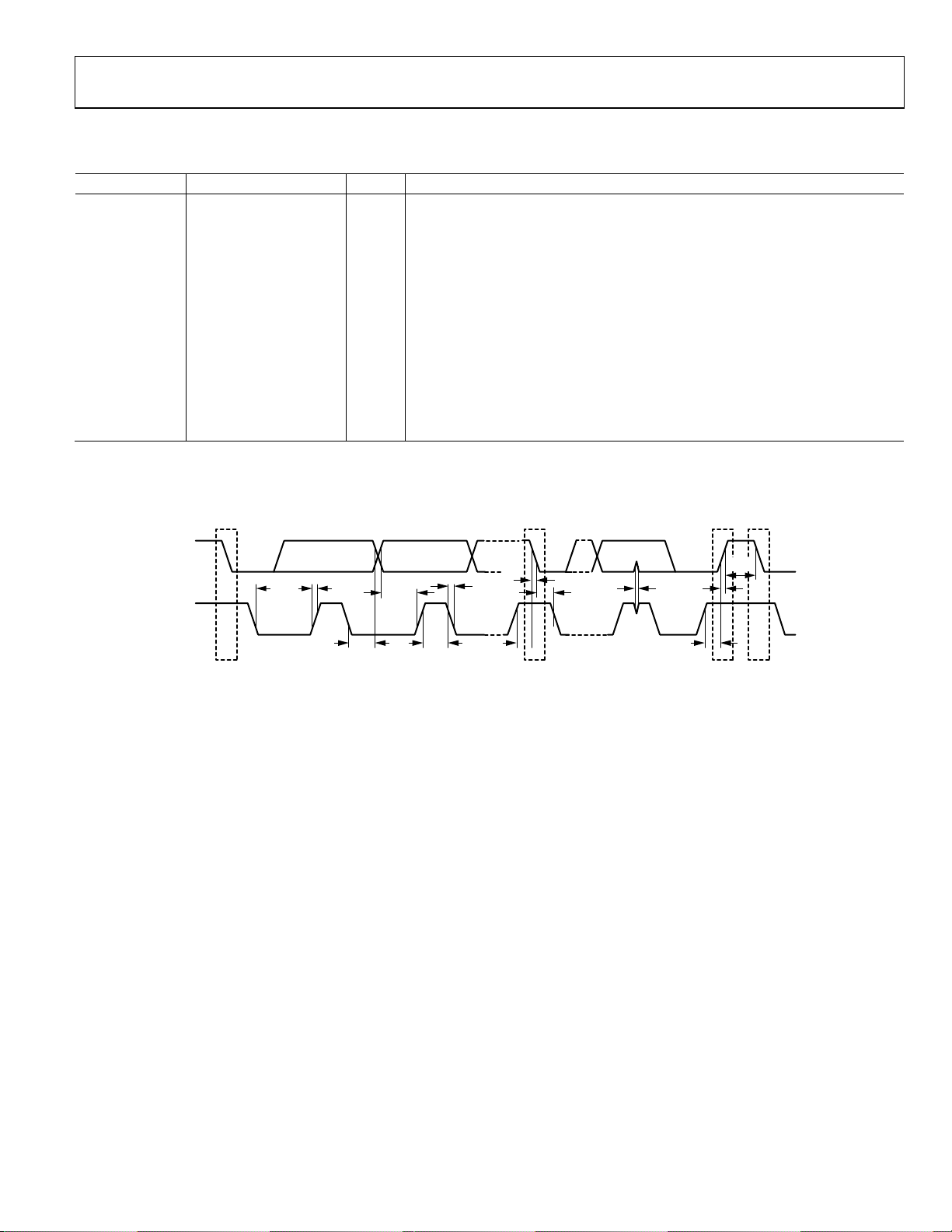
I2C TIMING SPECIFICATIONS
Table 6.
Parameter Min Max Unit Description
f
SCL
t
HIGH
t
LOW
t
SU,DAT
1
t
0 0.9 μs Data hold time
HD,DAT
t
SU,STA
t
HD,STA
t
BUF
t
SU,STO
t
20 + 0.1CB 300 ns Rise time of SCL/SDA
RISE
t
20 + 0.1C
FAL L
t
SP
2
C
B
1
A master device must provide a hold time of at least 300 ns for the SDA signal (referred to the V
2
CB is the total capacitance of one bus line in picofarads (pF).
Timing Diagram
400 kHz SCL clock frequency
0.6 μs SCL high time
1.3 μs SCL low time
100 ns Data setup time
0.6 μs Setup time for repeated start
0.6 μs Hold time for start/repeated start
1.3 μs Bus free time between a stop condition and a start condition
0.6 μs Setup time for stop condition
300 ns Fall time of SCL/SDA
B
0 50 ns Pulse width of suppressed spike
400 pF Capacitive load for each bus line
of the SCL signal) to bridge the undefined region of the SCL falling edge.
IHMIN
SDA
t
LOW
SCL
t
S
S = START CONDI TION
Sr = START REPE ATED CO NDITI ON
P = STOP CO NDITION
HD,DAT
t
RISE
t
SU,DAT
Figure 3. I
t
FALL
t
t
SU,STA
HIGH
2
C Interface Timing Diagram
t
t
FALL
t
HD,STA
Sr P S
tSPt
t
SU,STO
RISE
BUF
07774-003
Rev. 0 | Page 7 of 28
Page 8
ADP5020
ABSOLUTE MAXIMUM RATINGS
Table 7.
Parameter Rating
VDD1, VDD2, VDD3 −0.3 V to +6 V
SW1, SW2 −0.3 V to +6 V
VOUT1, VOUT2, VOUT3 −0.3 V to +6 V
VDD_IO −0.3V to +3.6 V
EN, SCL, SDA, SYNC, XSHTDN −0.3 V to V
Operating Temperature Range
Ambient −40°C to +85°C
Junction −40°C to +125°C
Storage Temperature Range −65°C to +150°C
Lead Temperature 260°C
Soldering (10 sec) 260°C
Vapor Phase (60 sec) 215°C
Infrared (15 sec) 220°C
V
ESD
Machine Model Range −200 V to +200 V
Human Body Model Range −2000 V to +2000 V
Charged Device Model ±750 V
DD_IO
+ 0.3 V
Stresses above those listed under Absolute Maximum Ratings
may cause permanent damage to the device. This is a stress
rating only; functional operation of the device at these or any
other conditions above those indicated in the operational
section of this specification is not implied. Exposure to absolute
maximum rating conditions for extended periods may affect
device reliability.
The ADP5020 can be damaged when the junction temperature
(T
) limits are exceeded. Monitoring the ambient temperature
J
does not guarantee that T
is within the specified temperature
J
limits. In applications with high power dissipation and poor
thermal resistance, the maximum ambient temperature may
have to be derated. In applications having moderate power dissipation and low PCB thermal resistance, the maximum ambient
temperature can exceed the maximum limit as long as the junction
temperature is within specification limits. The T
dependent on the ambient temperature (T
A
of the device is
J
), the power dissipation
(PD) of the device, and the junction-to-ambient thermal resistance
of the package (θ
). Maximum TJ is calculated from TA and PD
JA
using the following formula:
T
= TA + (PD × θJA)
J
THERMAL RESISTANCE
θJA is specified for the worst-case conditions, that is, a device
soldered in a circuit board for surface-mount packages.
Table 8. Thermal Resistance
Package Type θJA θ
20-Lead LFCSP (CP-20-4) 47.4 4.3 °C/W
Unit
JC
Thermal Data
Junction-to-ambient thermal resistance (θJA) of the package is
based on modeling and calculation using a 4-layer board. The
junction-to-ambient thermal resistance is highly dependent on
the application and board layout. In applications where high maximum power dissipation exists, attention to thermal board design
is required. The value of θ
may vary, depending on PCB material,
JA
layout, and environmental conditions. The specified value of θ
is based on a 4-layer, 4 in × 3 in, 2 1/2 oz copper board, as per
JEDEC standards. For more information, see the AN-772
Application Note, A Design and Manufacturing Guide for the
Lead Frame Chip Scale Package (LFCSP).
ESD CAUTION
JA
Rev. 0 | Page 8 of 28
Page 9

ADP5020
PIN CONFIGURATION AND FUNCTION DESCRIPTIONS
1
2
SW
VDD1
SW
PGND1
VDD2
19
20
18
17
16
15VOUT1
14VOUT1
13VDD3
12VOUT3
11EN/GPIO
NOTES
1. EXPOSED PAD SHOULD BE CO NNECTED
TO PGND1 AND PGND2.
ADP5020
BOTTOM VIEW
(Not to Scale)
EXPOSED PAD
8
9
10
SCL
VDD_IO
XSHTDN
Figure 4. Pin Configuration (Bottom View)
1 PGND2
2VOUT2
3 VDDA
4AGND
5SYNC
6
7
SDA
GND
D
07774-004
Table 9. Pin Function Descriptions
Pin No. Mnemonic Description
1 PGND2 Power Ground Buck 2.
2 VOUT2 Feedback Buck 2.
3 VDDA Supply Voltage Internal Analog Circuit.
4 AGND Analog Ground.
5 SYNC
Frequency Synchronization. Connect to an external 19.2 MHz or 9.6 MHz clock signal to synchronize the
internal oscillator.
6 DGND Digital Ground.
7 SDA I2C Data.
8 SCL I2C Clock.
9 VDD_IO Supply Voltage for Internal Logic Inputs/Outputs.
10 XSHTDN Shutdown Output, Active Low.
11 EN/GPIO
After power-on reset, this pin is defined as enable (EN). To enable active high, the I
this pin to be an output (GPIO). A weak pull-down resistor is enabled when the pin operates as EN.
12 VOUT3 Regulated Output Voltage from LDO.
13 VDD3 Supply Voltage LDO.
14, 15 VOUT1 Feedback/Driver Buck 1 Output.
16 PGND1 Power Ground Buck 1.
17 SW1 Switch Pin Buck 1.
18 VDD1 Supply Voltage Buck 1.
19 VDD2 Supply Voltage Buck 2.
20 SW2 Switch Pin Buck 2.
EPAD Exposed paddle Exposed pad should be connected to PGND1 and PGND2.
2
1
VDD1
VDD2
SW
20
PIN 1
PGND2
VOUT2
VDDA
AGND
SYNC
1
2
3
4
5
INDICATOR
ADP5020
TOP VIEW
(Not to Scale)
6
DGND
Figure 5. Pin Configuration (Top View)
PGND1
SW
17
16
18
19
15
VOUT1
14
VOUT1
13
VDD3
VOUT3
12
11
EN/GPIO
9
8
7
10
SCL
SDA
VDD_IO
XSHTDN
2
C command can program
07774-005
Rev. 0 | Page 9 of 28
Page 10

ADP5020
TYPICAL PERFORMANCE CHARACTERISTICS
VIN = 4.5 V, V
3.5
3.0
2.5
= 2.8 V, V
OUT1
OUT2
= V
3.3V
3.0V
2.8V
2.5V
OUT3
= 1.8 V, I
= 100 mA, C4 = C1 = 10 μF, C2 = 4.7 μF, C3 = 1 μF, TJ = 25°C, unless otherwise noted.
OUT
95
90
85
2.0
LDO VOLTAGE (V)
1.5
1.0
0 30 60 90 120 150
2.0V
1.8V
LOAD CURRENT (mA)
Figure 6. LDO Load Regulation
LDO OUTPUT = 20mV/DIV
I
= 100mA/DIV
LOAD
TIME = 100µs/DIV
LDO
I
LOAD
Figure 7. LDO Load Transient
V
80
EFFICIENCY (%)
75
70
0 100 200 300 400 500 600
07774-006
LOAD CURRENT (mA)
V
V
V
V
V
V
OUT1
OUT2
OUT3
OUT4
OUT5
OUT6
OUT7
(2.5V)
(2.8V)
(2.9V)
(3.0V)
(3.2V)
(3.3V)
(3.7V)
07774-009
Figure 9. Buck 1, Efficiency vs. Load Current
BUCK 1 OUTPUT = 100mV /DIV
= 100mA/DIV
I
LOAD
TIME = 100µs/DIV
BUCK 1
I
LOAD
07774-007
07774-010
Figure 10. Buck 1 Load Transient Response
3.8
V
(3.7V)
3.6
3.4
3.2
3.0
2.8
2.6
OUTPUT VOLTAGE (V)
2.4
2.2
0
0 100 200 300 400 500 600
OUT7
V
(3.3V)
OUT6
V
(3.0V)
OUT4
V
(2.8V)
OUT2
V
(2.5V)
OUT1
LOAD CURRENT (mA)
V
V
OUT5
OUT3
(3.2V)
(2.9V)
Figure 8. Buck 1 Load Regulation
07774-008
Rev. 0 | Page 10 of 28
1.9
1.8
1.7
1.6
1.5
1.4
1.3
OUTPUT VOLTAGE (V)
1.2
1.1
0
0 50 100 150 200 250 300
LOAD CURRENT (mA)
V
V
V
V
V
V
V
V
OUT8
OUT7
OUT6
OUT5
OUT4
OUT3
OUT2
OUT1
(1.8V)
(1.7V)
(1.6V)
(1.5V)
(1.4V)
(1.3V)
(1.2V)
(1.1V)
Figure 11. Buck 2 Load Regulation
07774-011
Page 11

ADP5020
VIN = 4.5 V, V
0.90
0.85
0.80
= 2.8 V, V
OUT1
OUT2
= V
OUT3
= 1.8 V, I
= 100 mA, C4 = C1 = 10 μF, C2 = 4.7 μF, C3 = 1 μF, TJ = 25°C, unless otherwise noted.
OUT
BUCK 1 OUTPUT = 2V /DIV
BUCK 2 OUTPUT = 1V /DIV
0.75
0.70
0.65
EFFICIENCY (%)
0.60
0.55
0.50
0 50 100 150 200 250 300
LOAD CURRENT (mA)
EFF1 (1.1V)
EFF2 (1.2V)
EFF3 (1.3V)
EFF4 (1.4V)
EFF5 (1.5V)
EFF6 (1.6V)
EFF7 (1.7V)
EFF8 (1.8V)
Figure 12. Buck 2 Efficiency vs. Load Current
BUCK 2 OUTPUT = 50mV /DIV
= 100mA/DIV
I
LOAD
TIME = 100µ s/DIV
BUCK 2
I
LOAD
TIME = 5ms/DIV
BUCK 2
ENABLE
07774-015
07774-012
Figure 15. Startup Sequence of the Three Regulators, Set by Default
BUCK 2 OUTPUT = 1V /DIV
SW2 OUTPUT = 2V/DIV
TIME = 500µ s/DIV
BUCK 2
SW2
Figure 13. Buck 2 Load Transient Response
1.2
1.0
0.8
0.6
0.4
SHUTDOWN CURRENT ( µA)
0.2
0
2.0 2.5 3.0 3.5 4.0 4.5 5.0
I
(µA) @ –40°C
SHTDN
(µA) @ +25°C
I
SHTDN
(µA) @ +125°C
I
SHTDN
INPUT VOLTAGE (V)
Figure 14. Shutdown Current vs. Input Voltage
07774-013
Figure 16. Buck 2 Enable Startup
BUCK 1 OUTPUT = 1V /DIV
SW1 OUTPUT = 2V/DIV
TIME = 500µ s/DIV
BUCK 1
SW1
07774-014
Figure 17. Buck 1 Enable Startup
07774-016
07774-017
Rev. 0 | Page 11 of 28
Page 12

ADP5020
VIN = 4.5 V, V
= 2.8 V, V
OUT1
= V
OUT2
LDO OUTPUT = 1V/DIV
TIME = 50µs/DIV
OUT3
= 1.8 V, I
= 100 mA, C4 = C1 = 10 μF, C2 =4.7 μF, C3 = 1 μF, TJ = 25°C, unless otherwise noted.
OUT
SW2
LDO
Figure 18. LDO Startup
SW1
BUCK 1 OUTPUT = 20mV/DIV
SW1 = 5V/DIV
TIME = 100ns/DIV
BUCK 1
Figure 19. Buck 1 Switching Node Voltage and
Output Ripple Voltage
BUCK 2 OUTPUT = 20mV/DIV
SW2 = 5V/DIV
TIME = 100ns/DIV
BUCK 2
07774-028
07774-030
Figure 20. Buck 2 Switching Node Voltage and
Output Ripple Voltage
BUCK 1 OUTPUT = 2V/ DIV
BUCK 2 OUTPUT = 1V/ DIV
LDO OUTPUT = 1V/DIV
BUCK 1
LDO
BUCK 2
ENABLE
07774-029
ENABLE OUTPUT = 2V/DIV
TIME = 5ms/DIV
07774-031
Figure 21. Three Regulators Turned Off by Sequencer
Rev. 0 | Page 12 of 28
Page 13

ADP5020
THEORY OF OPERATION
CIRCUIT OPERATION
The buck converters use pMOSFET as the upper switch and
nMOSFET as a synchronous rectifier. This synchronous rectification maintains high efficiency for a wide input and output
voltage range. The voltage mode control architecture, which
features a high frequency bandwidth, provides a fast load and
line transient response. The Buck 1 regulator can deliver up to
600 mA with very tight regulation. To minimize cross conduction
and maximize efficiency, an antishoot-through circuit is implemented in the gate driver. The two switching regulators operate
out of phase, reducing input ripple voltage and current.
INTERNAL COMPENSATION
The ADP5020 contains an internal compensation network. The
compensation circuit is designed to make the synchronous buck
converter stable over the input line, output load, and temperature
with specified output capacitors and inductors. In addition, the
high bandwidth control loop design allows for fast load and line
transient response.
CURRENT LIMITING AND SHORT-CIRCUIT PROTECTION
Both buck converters and the LDO have a current limit feature
that allows the ADP5020 to protect itself and any external components during overload and short-circuit conditions. The upper
switch pMOSFET turns off if peak current exceeds the limit.
The nMOSFET is turned on for a longer period until inductor
current drops to 0 A to prevent thermal runaway.
SYNCHRONIZATION
The device has several methods of synchronizing an external
clock with the switching regulators. If the external clock is
9.6 MHz, Bit 6 (SYNC_9P6) in the OPERATIONAL_CONTROL
register (Address 0x04) must be set to 1, and Bit 5 (SYNC_19P2)
must be set to 0. This operation divides the external clock by 3
before it is applied to the switching regulator clock. If the external
clock is 19.2 MHz, Bit 5 (SYNC_19P2) in Address 0x04 must be
set to 1, and Bit 6 (SYNC_9P6) must be set to 0. This opera-tion
divides the external clock by 6 before it is applied to the
switching regulator clock. The synchronous clock can be dc- or
ac-coupled onto the SYNC pin. For ac coupling, Bit 4 (SYNC_AC)
in Address 0x04 is set to 1; for dc coupling, Bit 4 is set to 0.
Operational control is performed by I
I2C INTERFACE
An internal register can be accessed using a synchronous
serial interface that implements the standard I
ADP5020 behaves as a slave device, communicating at normal
speed (100 kHz) or fast speed (400 kHz).
2
C writing to Register 0x04.
2
C interface. The
2
The I
C timing specifications are shown in Tab l e 6, and the I2C
interface timing diagram is shown in Figure 3. The 7-bit slave
address of the ADP5020 is shown in Ta b le 1 0 .
UNDERVOLTAGE LOCKOUT
The undervoltage lockout block contains the UVLO detector
circuits for the battery voltage level. It also contains the status
registers that are required to allow the external application
processor to determine the status of the power supplies. The
most important function of the UVLO circuit is to prevent
converter operation if the supply voltage is too low. The UVLO
falling condition (when the battery voltage decreases from the
operating range level) is set to a typical value of 2.0 V, whereas the
UVLO rising condition (when the supply voltage increases from
zero) is typically 2.2 V.
THERMAL SHUTDOWN
The thermal shutdown block (TSD) prevents device damage
if the die temperature reaches a level greater than 150°C. When
the thermal shutdown limit is reached, the regulator disables
the outputs, while waiting for the die to cool down (typically, to
30°C below the thermal shutdown threshold). There are two
distinct conditions to be considered when recovering from
a thermal shutdown condition:
• The EN pin is low. If the EN pin is low and the device is
operating in I
disabled until the application processor initializes the
parameters and performs the sequencing of the regulators.
The application processor can sense a generic failure condition by detecting a missing acknowledge bit following an
2
I
C command. When a thermal shutdown condition occurs,
Bit 0 (TSD) in the OPERATIONAL_CONTROL register
(Address 0x04) is latched to 1 so that the processor can
recognize the origin of the failure when resuming from
a fault condition. When the TSD bit is set, the application
processor must clear this bit to activate the regulators. If
the TSD bit is not cleared, writing to the regulator enable
bits, Bits[7:4] (BK1_EN, BK2_EN, LDO_EN, and EN_ALL),
in the REG_CONTROL_STATUS register (Address 0x03)
has no effect. The application processor can also force Bit 0
(TSD) to 1. In this case, the operation proceeds as though
a thermal shutdown condition has occurred.
• The EN pin is high. If the EN pin is high, the device resumes
operation automatically from a thermal shutdown condition.
The device resumes performing the predefined regulator
sequence without processor intervention. Bit 0 (TSD) in the
OPERATIONAL_CONTROL register (Address 0x04) is set
to indicate that a thermal shutdown has occurred, and it is
not possible to activate the regulators using an I
mand unless the host sets the TSD bit to 0.
2
C command mode, the outputs remain
2
C com-
Rev. 0 | Page 13 of 28
Page 14

ADP5020
CONTROL REGISTERS
DEVICE ADDRESS
Following a start condition, the bus master must send the address
of the slave it is accessing. The slave address for the ADP5020 is
shown in Tab l e 10 . The Bit 0 defines the operation to be per-
Table 10. Slave Address
Bit 7 Bit 6 Bit 5 Bit 4 Bit 3 Bit 2 Bit 1 Bit 0
ADR6 ADR5 ADR4 ADR3 ADR2 ADR1 ADR0 R/W
0 0 1 0 1 0 0 1 or 0
REGISTER MAP
Table 11.
Address Register Name D7 D6 D5 D4 D3 D2 D1 D0
0x00 Revision MAJ[2:0] MIN[2:0] OPT[1:0]
0x01 BUCK1_VSEL Reserved[7:3] BK1_VSEL[2:0]
0x02 BUCK2_LDO_VSEL BK2_VSEL[3:0] LDO_VSEL[3:0]
0x03
0x04
0x05
0x06 to
0x0F
REG_CONTROL_STATUS BK1_EN BK2_EN LDO_EN EN_ALL
OPERATIONAL_CONTROL Reserved SYNC_9P6 SYNC_19P2
EN_CONTROL Reserved[7:2]
Reserved
formed. When this bit is set to Logic 1, a read operation is
selected. When this bit is set to Logic 0, a write operation is
selected.
FORCE_XS
TSD
ENO_DRV
SYNC_
AC
BK1_
PGOOD
BK1_
XSHTDN
BK2_
PGOOD
BK2_
XSHTDN
LDO_
PGOOD
LDO_
XSHTDN
ENO_HIZ_
BAR
REGISTER DESCRIPTIONS
User Accessible Registers
Table 12. Revision Register, Address 0x00
Bit Bit Name Access Default Description
[7:5] MAJ[2:0] R N/A Major revision bits. Used to electronically ID the device version.
[4:2] MIN[2:0] R N/A Minor revision bits. Used to electronically ID the device version.
[1:0] OPT[1:0] R N/A Option bits. Used to electronically ID the option (multiple options on same device family).
Table 13. BUCK1_VSEL Register, Address 0x01
Bit Bit Name Access Default Description
[7:3] Reserved N/A N/A Reserved.
[2:0] BK1_VSEL[2:0] R/W Fuse
000 = 2.5 V.
001 = 2.8 V.
010 = 2.9 V.
011 = 3.0 V.
100 = 3.2 V.
101 = 3.3 V (default).
110 = 3.7 V.
111 = reserved.
Sets the voltage output level of the Buck 1 regulator. Preloads on power-up with values
stored in fuses. Note that this value can be edited by the user in an application.
Rev. 0 | Page 14 of 28
Page 15

ADP5020
Table 14. BUCK2_LDO_VSEL Register, Address 0x02
Bit Bit Name Access Default Description
[7:4] BK2_VSEL[3:0] R/W Fuse
0000 = 1.1 V.
0001 = 1.1 V.
0010 = 1.1 V.
0011 = 1.1 V.
0100 = 1.1 V.
0101 = 1.1 V.
0110 = 1.1 V.
0111 = 1.1 V.
1000 = 1.1 V.
1001 = 1.2 V (default).
1010 = 1.3 V.
1011 = 1.4 V.
1100 = 1.5 V.
1101 = 1.6 V.
1110 = 1.7 V.
1111 = 1.8 V.
[3:0] LDO_VSEL[3:0] R/W Fuse
0000 = 1.8 V (default).
0001 = 1.9 V.
0010 = 2.0 V.
0011 = 2.1 V.
0100 = 2.2 V.
0101 = 2.3 V.
0110 = 2.4 V.
0111 = 2.5 V.
1000 = 2.6 V.
1001 = 2.7 V.
1010 = 2.8 V.
1011 = 2.9 V.
1100 = 3.0 V.
1101 = 3.1 V.
1110 = 3.2 V.
1111 = 3.3 V.
Sets the voltage output level of the Buck 2 regulator. Preloads on power-up with values
stored in fuses. Note that this value can be edited by a user in an application.
Sets the voltage output level of the LDO regulator. Preloads on power-up with values
stored in fuses. Note that this value can be edited by the user in an application.
Rev. 0 | Page 15 of 28
Page 16

ADP5020
Table 15. REG_CONTROL_STATUS Register, Address 0x03
Bit Bit Name Access Default Description
7 BK1_EN R/W 0 1 = turns on the Buck 1 regulator. If the EN pin is high, the sequencer is ignored.
6 BK2_EN R/W 0 1 = turns on the Buck 2 regulator. If the EN pin is high, the sequencer is ignored.
5 LDO_EN R/W 0 1 = turns on the LDO regulator. If the EN pin is high, the sequencer is ignored.
4 EN_ALL R/W 0
3 BK1_PGOOD R 0 Power good status for Buck 1.
1 = power good (POK).
0 = fail.
2 BK2_PGOOD R 0 Power good status for Buck 2.
1 = power good (POK).
0 = fail.
1 LDO_PGOOD R 0 Power good status for LDO.
1 = power good (POK).
0 = fail.
0 FORCE_XS R/W 0 1 = the XSHTDN pin is controlled by the power good signals.
0 = the XSHTDN pin is held low unless the EN pin is high, regardless of regulator status.
If EN is high, this bit is ignored in controlling the XSHTDN pin (acts as if FORCE_XS = 1).
Table 16. OPERATIONAL_CONTROL Register, Address 0x04
Bit Bit Name Access Default Description
7 Reserved N/A N/A Reserved.
6 SYNC_9P6
5 SYNC_19P2
1
R/W 0
1
R/W 0
1 for both SYNC_9P6 and SYNC_19P2 = invalid setting.
4 SYNC_AC
1
R/W 0 1 = the ac path is used for the SYNC input.
0 = the dc path is used (default).
3 BK1_XSHTDN R/W Fuse 0 = power good for Buck 1 must be high for XSHTDN to go high (default).
1 = Buck 1 power good is ignored.
2 BK2_XSHTDN R/W Fuse 0 = power good for Buck 2 must be high for XSHTDN to go high (default).
1 = Buck 2 power good is ignored.
1 LDO_XSHTDN R/W Fuse 0 = LDO power good must be high for XSHTDN to go high (default).
1 = LDO power good is ignored.
0 TSD R/W 0 Shows a latched status of a thermal shutdown (TSD) event.
1 = TSD is active.
1
The SYNC selection bits (SYNC_AC, SYNC_9P6, and SYNC_19P2) cannot be changed while a switching regulator is running.
1 = turns on all regulators, following sequencer programming. BK1_EN, BK2_EN, and
LDO_EN must all be set to 0 for this bit to function.
1 = a 9.6 MHz clock is on the SYNC pin. The SYNC frequency is divided by 3 and used as
clock frequency for switching regulators.
1 = a 19.2 MHz clock is on the SYNC pin. The SYNC frequency is divided by 6 and used as
clock frequency for switching regulators.
0 for both SYNC_9P6 and SYNC_19P2 = clock synchronization is disabled, and the device
operates with the 3 MHz internal clock.
Must be cleared to 0 by user program to enable the regulators. If this bit remains set to 1,
regulator activation is inhibited, as in a thermal shutdown event.
Table 17. EN_CONTROL Register, Address 0x05
Bit Bit Name Access Default Description
[7:2] Reserved N/A N/A Reserved.
1 ENO_HIZ_BAR R/W 0 0 = the EN/GPIO pin is in high impedance, and the EN function is selected.
1 = GPIO output is selected, and the EN function is ignored.
0 ENO_DRV R/W 0 Active only when ENO_HIZ_BAR = 1 (GPIO).
0 = GPIO output is set to low.
1 = GPIO output is set to high.
Rev. 0 | Page 16 of 28
Page 17

ADP5020
POWER-UP/POWER-DOWN SEQUENCE
SEQUENCER
The sequencer is enabled after a low-to-high transition of the
enable pin (EN). When EN is low or programmed as an output, the
sequencing is controlled and timed by the application processor
via the I
Each regulator inside the ADP5020 is controlled by the
sequencer block. The sequencer is factory programmed with
a default turn-on sequence that determines the activation order of
the regulators. The default activation order is listed as follows:
1. Buck 1
2. LDO
3. Buck 2
A low-to-high transition of the EN pin, when programmed
as an input, or an I
REG_CONTROL_STATUS register (Address 0x03), starts the
sequencer.
The activation delay for the first regulator is determined by the
turn-on delay of the band gap, oscillator, and other internal
circuits. Therefore, the first regulator cannot be activated before
a typical 5 ms delay time has elapsed. Delays between the first
and second regulator and from the second to third regulator are
hard coded to a specific time (t
time starts from the moment a regulator has reached the power
good threshold (see Figure 22).
2
C commands.
2
C command setting Bit 4 (EN_ALL) in the
REG1
, t
REG2
, and t
). The delay
REG3
DEFAULT POWER-ON SEQUENCE WITH EN PIN
Figure 22 shows the default regulator sequencing after a low-tohigh transition of the EN pin. The regulator order is factory
programmed and can be changed for specific applications. The
power good signal (POK) turns to high if the regulator voltage
is ≥80% of the target voltage. The second regulator checks the
POK signal of the first regulator and waits the preset delay time
(t
) before turning on. In addition to changing the regulator
REG2
order, it is also possible to disable the unused regulator. Additional
fuses allow disabling of the association between XSHTDN generation and the POK signal for a specific regulator. The power good
signal of an unused regulator must be masked, via dedicated fuse
and user registers, to prevent the XSHTDN output from being
forced low. A host processor controller, connected to the I
can override the masking fuses by accessing the following bits in
the OPERATIONAL_CONTROL register (Address 0x04): Bit 3
(BK1_XSHTDN, for Buck 1), Bit 2 (BK2_XSHTDN, for Buck 2),
and Bit 3 (LDO_XSHTDN, for LDO). Writing 0 to these register
bits requires that power good be true to release the XSHTDN pin
to high. Writing 1 to these bits causes the regu-lator state to be
ignored, and XSHTDN must depend on the active and
unmasked regulators.
The regulators can also be activated individually via the I
commands. The host specifies which regulator is to be turned
on or off by setting or clearing the following selection bits in the
REG_CONTROL_STATUS register (Address 0x03): Bit 7
(BK1_EN), Bit 6 (BK2_EN), or Bit 5 (LDO_EN). When the
regulators are individually activated by I
2
C commands, the auto
sequencing is disabled and the host controls the turn-on and
turn-off timing (see Figure 26).
2
C bus,
2
C
EN
t
REG1
BUCK 1
LDO
BUCK 2
XSHTDN
Figure 22. Automatic Sequencing with EN Low-to-High Transition
POK
t
REG2
Rev. 0 | Page 17 of 28
t
REG3
POK
POK
t
XSHTDN
07774-018
Page 18

ADP5020
Activation Waveforms
VDDx
POR
INTERNAL
POR
EN
2
I
C BUS
BUCK 1
LDO
BUCK 2
XS
HTDN
VDDx
V
UVLOR
2
C SEQUENCER
I
REGISTERS
PROGRAMMING
EN_
ALL = 1
t
REG1
POK
t
REG2
Figure 23. Regulators Are Activated by I
t
REG3
POK
POK
t
XSHTDN
2
C Command
EN_
ALL = 0
07774-019
POR
INTERNAL
POR
EN
2
C SEQUENCER
I
2
C BUS
I
BUCK 1
BUCK 2
HTDN
XS
LD
O
REGIS TERS
PROGRAMMING
t
REG1
t
REG2
Figure 24. Activation Command Using the EN Pin
When activated through the EN pin, the sequencer is affected
2
only by the I
C commands that set or clear the regulator power
good masking bits: Bit 3 (BK1_XSHTDN), Bit 2 (BK2_XSHTDN),
and Bit 1 (LDO_XSHTDN) in the OPERATIONAL_CONTROL
register (Address 0x04). See the Default Power-On Sequence with
EN Pin section for more information. The sequence order of the
regulators is factory programmed through fuses, but the delays
POK
POK
t
REG3
POK
t
XSHTDN
07774-020
between the regulators (t
REG1
, t
REG2
, and t
) are fixed and cannot
REG3
be changed.
The EN_ALL bit (Bit 4) in the REG_CONTROL_STATUS regi-ster
(Address 0x03) has the same functionality as the EN pin. The
sequencer has an antiglitch function that allows it to ignore supply
voltage dip if glitch time is less than 50 μs (see Figure 25).
Rev. 0 | Page 18 of 28
Page 19

ADP5020
POWER-ON SEQUENCE USING THE I2C INTERFACE
When the EN pin is low, the regulator sequence is controlled by
the application processor sending I
activation. When Bit 4 (EN_ALL) in the REG_CONTROL_
STATUS register (Address 0x03) is set to 1, the regulator sequence
is as follows:
VDDx
POR
INTERNAL
POR
EN
2
I
C BUS
BUCK 1
LDO
2
C commands to control the
V
UVLOR
2
C SET/CLEAR
I
xxx_XSHTDN BITS
t
REG1
t
REG2
1. Buck 1
2. LDO
3. Buck 2
This sequence can be factory programmed through fuses.
Unused regulators can also be fuse programmed to be turned
off during sequencing.
V
<50µs
t
REG3
UVLOF
t
BUCK 2
XS
HTDN
XSHTDN
07774-021
Figure 25. Activation and Power Failure Conditions
EN
2
C BUS
I
BUCK 1
LDO
BUCK 2
XSHTDN
BK1_EN
= 1
LD0_EN
= 1
BK2_EN
= 1
FORCE_XS
Figure 26. Individual Activation Through I
= 1
2
C Commands
FORCE_XS
= 0
BK1_EN,
LDO_EN,
BK2_EN = 0
07774-022
Rev. 0 | Page 19 of 28
Page 20

ADP5020
The application processor, together with the regulator power
good signal, controls the XSHTDN pin, as shown in Tabl e 18 .
After a regulator is enabled and no failure condition is detected
(power good = 1 in Bits[3:1] of the REG_CONTROL_STATUS
register, Address 0x03), the level of the XSHTDN pin is controlled by Bit 0 (FORCE_XS) in the REG_CONTROL_STATUS
register. Therefore, the application processor can write to this
register to gain control over the XSHTDN pin. However, if the
EN signal is high, the level on the XSHTDN pin depends on the
power good condition of the regulator.
Table 18. Truth Table
EN
Pin
2
C Regulator Enable
I
Power
Good
FORCE_XS
XSHTDN
Pin
0 0 0 X1 0
0 1 X1 0 0
0 1 0 1 0
0 1 1 1 1
1 X1 1 X1 1
1 X1 0 X1 0
1
X = don’t care.
POWER-UP/POWER-DOWN STATE FLOW
When the device is enabled, the UVLO circuit constantly monitors
UVLOR
UVLOF
),
the supply voltage. If the supply voltage falls below the V
threshold, typically 2.0 V, the regulators are immediately turned
off. All the internal analog circuits are then disabled to save power,
except the power-on reset (POR) circuit, which detects if the supply
voltage is dropping. If the supply voltage is higher than the POR
threshold, the POR circuit keeps the logic circuits operating
properly and retains the internal values of the registers. This
POR threshold is set to approximately 1.4 V.
If the supply voltage goes below the V
threshold, but not
UVLOR
below the POR threshold, the registers are preserved. If the supply
voltage returns to the normal operating level (above V
a new activation does not require initialization of the registers.
However, if the supply voltage goes below the POR level, the
device is held in reset state. When the input voltage resumes the
proper operating level, the host controller must reload the registers.
The additional current required to keep the POR monitoring
circuits alive during UVLO is estimated to be approximately 1 μA.
NO POWER
VDDx > V
POR
LEVEL
INTERNAL
RESET
EN = LOW
STAND BY
STARTUP
SEQUENCER
EN = LOW OR I2C OFF
COMMAND
OR VDDx < V
UVLOF
VDDx < V
EN = HIGH
POR
07774-023
EN = LOW AND 12C OFF
COMMAND
OR VDDx < V
NORMAL
OPERATIO N
END, AND ALL REG ULATIONS ARE
SEQUENCE
POWER GOOD
VDDx < V
UVLOF
I2C
COMMANDS
TSD
POR
DEVICE ENABLED
(EN_ALL OR E N = HIGH)
Figure 27. State Flow
Rev. 0 | Page 20 of 28
Page 21

ADP5020
APPLICATIONS INFORMATION
POWER GOOD STATUS
The ADP5020 constantly monitors the operating conditions.
When a regulator is activated, it checks if the output voltage
level is above 80% (the power good threshold) of the nominal
level for that output. If the output voltage does not reach the
power good threshold, one of the three power good status bits in
the REG_CONTROL_STATUS register (Address 0x03) is cleared.
If the output voltage reaches the power good threshold, one of
the power good status bits in the REG_CONTROL_STATUS
register is set to 1. The REG_CONTROL_STATUS register
contains the following three power good bits: BK1_PGOOD for
the Buck 1 output (Bit 3), BK2_PGOOD for the Buck 2 output
(Bit 2), and LDO_PGOOD for the LDO output (Bit 1).
XSHTDN LOGIC
In addition to the power good information for each enabled
regulator, an XSHTDN signal is generated, as shown in Tab l e 18 . If
one or more regulators are unused in a specific application, the
masking bits for the disabled regulator, which are fuse programmable and I
2
C programmable after device startup, must be
set to 1 to mask the status of the power good signal. Besides having
the masking bits predefined through factory-programmed fuses
(necessary only for operation with the EN signal), the ADP5020
provides three masking bits that are accessible through the I
2
C
interface. These bits are located in the OPERATIONAL_
CONTROL register (Address 0x04), where the BK1_XSHTDN
bit (Bit 3) is the mask (if set to 1) for Buck 1, the BK2_XSHTDN bit
(Bit 2) is the mask (if set to 1) for Buck 2, and the LDO_
XSHTDN bit (Bit 3) is the mask (if set to 1) for the LDO. Additional failures that are verified are the input (VDDA) undervoltage
condition, as described in the Undervoltage Lockout section; and
an overtemperature condition of the die, as described in the
Thermal Shutdown section. As soon as one of these conditions
occurs, the active regulators are immediately turned off, and the
XSHTDN pin is set to 0.
COMPONENTS SELECTION
Buck Inductor
The buck inductor is chosen to meet output ripple current and
ripple voltage requirements with minimum size. The fast load
transient response and wide frequency bandwidth are also important factors for inductor selection. The minimum inductance of the
buck converter is derived from the following equation:
)(
×−
VVV
OUTOUTINMAX
L
MINBUCK
=
where:
V
is the maximum input supply voltage.
INMAX
V
is the regulator output voltage in the buck converter.
OUT
is the converter switching frequency.
f
SW
r is the inductor ripple factor, which is selected as 30%.
(1)
IrfV
×××
OUTSWINMAX
Peak inductor current is calculated in the following equation:
I
= I
LMAX
+ 0.5 × r × I
OUT
(2)
OUT
The calculated minimum Buck 2 inductor value is 2.2 μH. The
maximum peak inductor current is 325 mA. A ceramic inductor
such as the Taiyo Yuden BRL2012T2R2M, with a 600 mA saturation current in a 2 mm × 1.2 mm × 1 mm package, can be used.
For the Buck 1 converter, the calculated minimum inductance is
2.2 μH, with maximum peak current of 690 mA. A ceramic
inductor such as the Taiyo Yuden BRL2518T2R2M, with a 1 A
saturation current in a 2.5 mm × 1.8 mm × 1.2 mm package, is
recommended.
Input Capacitor Selection
The input capacitors are used to decouple the parasitic inductance
of input wires to the converters and to reduce the input ripple
voltage and the switching ac current flow to the battery rail. The
capacitors are selected to support the maximum input operating
voltage and the maximum rms current. The capacitance must also
be large enough to ensure input stability and suppress input ripple.
ESR should as small as possible to decouple the noise. MLCC
ceramic capacitors are a good choice for battery-powered applications because of their high capacitance, small size, and low ESR.
A 10 μF ceramic capacitor (for example, the JMK107BJ106MA-T
from Taiyo Yuden) is recommended.
Output Capacitor Selection
Output capacitor selection should be based on the following three
factors:
• Maximizing the control loop bandwidth of the converter
with the LC filter
• Minimizing the output voltage ripple
• Minimizing the size of the capacitor
Note that the output ripple is the combination of several factors,
including the inductor ripple current (ΔI
), the ESR and ESL
L
output capacitors, and the capacitor impedance at the switching
frequency.
In buck converters, the output ripple can be calculated as
follows:
ΔV
ΔI
OUTRIPPLE
= r × I
L
⎛
= ΔIL
⎜
ESR 4
+
⎜
⎝
OUT
1
8
Cf
××
OUTSW
⎞
⎟
fESL
××+
SW
⎟
⎠
Capacitor manufacturer data sheets show the ESR and ESL
value. In real-life applications, the ripple voltage may be higher
because the equations provided in this data sheet do not consider
parameters such as board/package parasitic inductance and
capacitance. The minimum recommended capacitance is no less
than 4.0 μF for Buck 1, 2.0 μF for Buck 2, and 0.4 μF for the
LDO.
Rev. 0 | Page 21 of 28
Page 22

ADP5020
LDO INPUT FILTER
To improve the LDO input-to-output ripple suppression in the
critical switching frequency range of the buck converters, it may be
necessary to add an LC filter tuned to 1 MHz, as shown in
Figure 28. Additional tests and simulation must be performed
to assess if this filter is necessary.
The filter resonance frequency is determined by the following
equation:
f
LC
1
where L3 = 250 nH, assuming that f
The inductor must be able to withstand the LDO load current,
including the overload condition, which is limited to 400 mA.
(3)
C8L3
××π×=2
= 1 MHz and C8 = 100 nF.
LC
VBATT
C1
10µF
ADP5020
SW1
L1
BUCK 1
LDO
VOUT1
VOUT1
10µF
VDD3
VOUT3
2.2µH
C6
L3
C8
0.1µF
C3
1µF
Figure 28. Optional LDO Input Filter
3.3V
INPUT FILTER
2.8V
LDO
07774-026
Rev. 0 | Page 22 of 28
Page 23

ADP5020
LAYOUT RECOMMENDATIONS
APPLICATIONS SCHEMATIC
ADP5020
INPUT POWER SUPPLIES
PROCESSOR
INTERFACE
GPIO/EN
VBATT
GND
VDDIO
SDA
SCL
SYNC
R1
10kΩR210kΩ
10µF
C4
C6
1.0µF
0.1µF
VDD1
SW1
BUCK 1BUCK 2LDO
VOUT1
VOUT1
PGND1
SW2
VOUT2
PGND2
VOUT3
XSHTDN
VDD2
VDD3
VDDA
VDD_IO
C5
SDA
SCL
SYNC
EN/GPIO
L1
2.2µH
L2
2.2µH
C1
10µF
C2
4.7µF
C3
1.0µF
+VIS
–VIS
+V
CORE
–V
CORE
+VIO
–VIO
XSHTDN
OUTPUT POW ER RAILS
DGND AGND
07774-027
Figure 29. Schematic for Camera Module Applications
Rev. 0 | Page 23 of 28
Page 24

ADP5020
PCB BOARD LAYOUT RECOMMENDATIONS
• Place the input and output capacitors, C1, C2, C3, C4, and
C5, as close as possible to the respective ADP5020 pin, and
make the grounding connection to the ADP5020 ground
pins as short as possible.
• Connect C3, C5, and C6 to the analog ground, and connect
C1, C2, and C4 to the power ground.
• Place the L1 and L2 inductors as close as possible to the
respective output pins.
EXTERNAL COMPONENT LIST
Table 19. Recommended External Components List
Reference
Designator Description Size Proposed Vendor Vendor Part No.
C1, C4 10 μF, X5R, 6.3 V, ±20% 0603 Murata GRM188R60J106M
C1, C4 10 μF, X5R, 6.3 V, ±20% 0603 Taiyo Yuden JMK107BJ106MA
C2 4.7 μF, X5R, 6.3 V, ±10% 0603 Murata GRM188R60J475K
C3 1.0 μF, X5R, 6.3 V, ±10% 0603 Murata GRM155R60J105K
C5 0.1 μF, X5R, 10 V, ±10% 0402 Murata GRM155R61A104K
C6 1.0 μF, X5R, 6.3 V, ±10% 0603 Murata GRM155R60J105K
L1 2.2 μH, DCR = 0.13 Ω, IDC = 1 A 2.5 mm × 1.8 mm × 1.2 mm Taiyo Yuden BRL2518T2R2M
L2 2.2 μH, DCR = 0.23 Ω, IDC = 0.53 A 2.0 mm × 1.2 mm × 1.0 mm Taiyo Yuden BRL2012T2R2M
R1, R2 10 kΩ, 1%, thick film resistor 0402 KOA Speer Electronics RK73H1ETTP1002F
• The power and analog ground planes are recommended to
keep the noise low. Use one layer for power ground and one
layer for analog ground. Tie the power and analog grounds
at a single point.
• Use wide traces to connect the inductor and the input and
output capacitors.
• Add the L3 inductor and the C8 capacitor, if needed, to
improve the LDO noise rejection at the switching frequency of the Buck 1 regulator (3 MHz) because the LDO
PSRR typically degrades at higher frequencies. If switching
noise is not an issue, remove the L3 inductor.
Rev. 0 | Page 24 of 28
Page 25

ADP5020
OUTLINE DIMENSIONS
0.08
0.50
BSC
0.50
0.40
0.30
0.60 MAX
15
11
P
N
I
N
I
2.65
2.50 SQ
2.35
0.25 MIN
D
16
10
20
EXPOSED
(BOTTOM VIEW)
1
PAD
5
6
FOR PRO P ER CONNECTION OF
THE EXPOSED PAD, REFER TO
THE PIN CONFIG UR ATION AND
FUNCTION DESCRIPTIONS
SECTION OF THIS DATA SHEET .
1
R
C
I
A
O
T
090408-B
4.00
PIN 1
INDICATOR
1.00
0.85
0.80
SEATING
PLANE
12° MAX
BSC SQ
TOP VIEW
0.80 MAX
0.65 TYP
0.30
0.23
0.18
COMPLIANT
0.60 MAX
3.75
BSC SQ
0.05 MAX
0.02 NOM
COPLANARITY
0.20 REF
TO
JEDEC STANDARDS M O-220-VGG D- 1
Figure 30. 20-Lead Lead Frame Chip Scale Package [LFCSP_VQ]
4 mm × 4 mm Body, Very Thin Quad
(CP-20-4)
Dimensions shown in millimeters
ORDERING GUIDE
Model Temperature Range Package Description Package Option
ADP5020ACPZ-R71 −40°C to +85°C 20-Lead Lead Frame Chip Scale Package [LFCSP_VQ] CP-20-4
ADP5020CP-EVALZ1 Evaluation Board
1
Z = RoHS Compliant Part.
Rev. 0 | Page 25 of 28
Page 26

ADP5020
NOTES
Rev. 0 | Page 26 of 28
Page 27

ADP5020
NOTES
Rev. 0 | Page 27 of 28
Page 28

ADP5020
NOTES
©2009 Analog Devices, Inc. All rights reserved. Trademarks and
registered trademarks are the property of their respective owners.
D07774-0-5/09(0)
Rev. 0 | Page 28 of 28
 Loading...