

Page 1
a
CDMA Power Management System
ADP3502
FEATURES
11 LDOs Optimized for Specific CDMA Subsystems
4 Backup LDOs for Standby Mode Operation
Ultra Low Standby Supply Current
High Accuracy Battery Charger (0.7%)
3 Li-Ion Battery Charge Modes
5 mA Precharge
Low Current Charge
Full Current Charge
Integrated RTC
Ambient Temperature: –30ⴗC to +85ⴗC
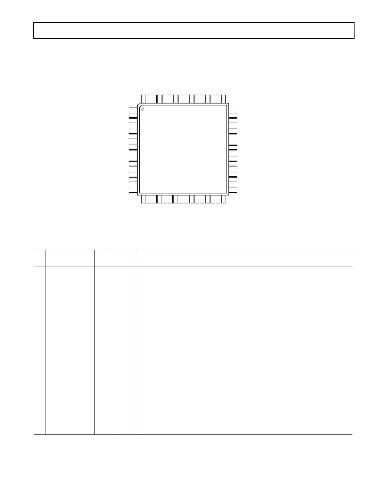
64-Lead 7 mm ⴛ 7 mm ⴛ 1 mm TQFP Package
APPLICATIONS
CDMA/CDMA2000/PCS Handsets
GENERAL DESCRIPTION
The ADP3502 is a multifunction chip optimized for CDMA-1x
cell phone power management. It offers a total power solution
for the handset baseband and RF section, including LDOs to
power 11 subsystems. Also integrated are a real-time clock
(RTC), serial bus interface, and charging control for Li-Ion/
Li-Polymer batteries. Sophisticated controls are available for
power-up during battery charging, keypad interface, GPIO/INT
function, and RTC function.
The ADP3502 is optimized for CDMA handsets powered by
single-cell Li-Ion batteries. Its high level of integration significantly reduces the design effort, number of discrete
components, and solution size/cost. The main-sub LDO
structure reduces the standby current consumption, and as a
result, greatly extends the standby time of the phone. System
operation has been proven to be fully compatible with
MSM51xx-based designs.
The ADP3502 comes in a 64-lead 7 mm × 7 mm × 1 mm
TQFP package and is specified over a wide temperature range of
–30°C to +85°C.
FUNCTIONAL BLOCK DIAGRAM
POWER ON
KEYPAD I/F
GPIO
SERIAL I/F
32kHz OUTPUT
CONTROL
RESET
OUTPUT
LOGIC
BLOCK
DELAY 10ms
INTERRUPT
CONTROL
LDO
CONTROL
RESET
RTC
COUNTER
STAY-ALIVE
TIMER
ANALOG
BLOCK
BATTERY
CHARGER
REFERENCE
LDO1 TO LDO11
VOLTA G E
DETECTOR
ADP3502
REV. 0
Information furnished by Analog Devices is believed to be accurate and
reliable. However, no responsibility is assumed by Analog Devices for its
use, nor for any infringements of patents or other rights of third parties that
may result from its use. No license is granted by implication or otherwise
under any patent or patent rights of Analog Devices. Trademarks and
registered trademarks are the property of their respective companies.
One Technology Way, P.O. Box 9106, Norwood, MA 02062-9106, U.S.A.
Tel: 781/329-4700 www.analog.com
Fax: 781/326-8703 © 2003 Analog Devices, Inc. All rights reserved.
Page 2

ADP3502–SPECIFICATIONS
MAIN FUNCTIONS
(TA = –30ⴗC to +85ⴗC, C
= 1 F MLCC, VBAT = 3.6 V, unless otherwise noted. See Table II for C
VBAT
OUT
.)
Parameter Symbol Conditions Min Typ Max Unit
SHUTDOWN GND CURRENT IGND
Power OFF TA = –20°C to +60°C2545µA
LDO3b: ON, Connect to RTCV
through Schottky Diode
RTC/32K OSC: Active
All Other LDOs: OFF
All Logic Inputs: VBAT or GND
MVBAT: OFF
OPERATING GND CURRENT IGND
Standby Mode Operation (Light Load) LDO1b, LDO2b, LDO3b, 60 125 µA
LDO6b: ON
= 1 mA for LDO3b and LDO6b
I
O
= 3 mA for LDO1b
I
O
I
= 300 µA for LDO2b
O
All Other LDOs: OFF
RTC/32K OSC: Active
MVBAT: OFF
All Logic Output: No Load
Standby Mode Operation (Midload) LDO1, LDO2, LDO3, LDO6, 300 µA
All Sub-LDOs: ON, I
= 70% Load
O
All Other LDOs: OFF
RTC/32K OSC: Active
MVBAT: ON
All Logic Outputs: No Load
Active Operation LDO5: OFF 700 µA
All Other LDOs: ON, 70% Load
RTC/32K OSC: Active
All Logic Outputs: No Load
MVBAT: ON
THERMAL SHUTDOWN THRESHOLD 160 °C
THERMAL SHUTDOWN HYSTERESIS 35 °C
ADAPTER/ADPSUPPLY VOLTAGE RANGE VADP 5 12 V
VBAT VOLTAGE RANGE VBAT 3.3 5.5 V
LDO SPECIFICATIONS
(TA = 25ⴗC, C
= 1 F MLCC, VBAT = V
VBAT
+ 1 V, NRCAP = 0.1 F. See Table II for C
OUT
OUT
.)
Parameter Symbol Conditions Min Typ Max Unit
BASEBAND VDD MAIN-LDO (LDO1a)
Output Voltage V
Output Capacitor Required for Stability C
Dropout Voltage V
LDO1aIO
LDO1a
DO
= 1 mA to 150 mA 2.81 2.90 2.99 V
= –30°C to +85°C
T
A
2.2 µF
IO = 150 mA 200 mV
Start-Up Time from Shutdown 250 µs
BASEBAND VDD SUB-LDO (LDO1b)
Output Voltage V
LDO1bIO
= 3 mA 2.8 2.87 3.0 V
TA = –30°C to +85°C
REV. 0–2–
Page 3

ADP3502
Parameter Symbol Conditions Min Typ Max Unit
BASEBAND AVDD MAIN-LDO (LDO2a)
Output Voltage V
Output Default Voltage V
Output Voltage V
Output Default Voltage V
Output Capacitor Required for Stability C
Dropout Voltage V
LDO2a
LDO2a
LDO2a
LDO2a
LDO2a
DO
Ripple Rejection f = 1 kHz 60 dB
Output Noise Voltage V
NOISE
Start-Up Time from Shutdown 250 µs
BASEBAND AVDD SUB-LDO (LDO2b)
Output Voltage V
LDO2b
REFO SWITCH
On Resistance R
Off Leak I
ON
LEAK
COIN CELL MAIN-LDO (LDO3a)
Output Voltage V
Dropout Voltage V
Output Capacitor Required for Stability C
LDO3a
DO
LDO3a
Start-Up Time from Shutdown 250 µs
COIN CELL SUB-LDO (LDO3b)
Output Voltage V
LDO3b
AUDIO LDO (LDO4)
Output Voltage V
Output Capacitor Required for Stability C
Dropout Voltage V
LDO4
LDO4
DO
Ripple Rejection f = 1 kHz 60 dB
Output Noise Voltage V
NOISE
Start-Up Time from Shutdown 250 µs
VIBRATOR LDO (LDO5)
Output Voltage V
Dropout Voltage V
Output Capacitor Required for Stability C
LDO5
DO
LDO5
BASEBAND CORE MAIN-LDO (LDO6a)
Output Voltage V
Output Capacitor Required for Stability C
Dropout Voltage V
LDO6a
LDO6a
DO
Start-Up Time from Shutdown 250 µs
16 Steps, 20 mV/Step, IO = 50 mA
Code: 1000 2.30 2.36 2.43 V
Code: 0111 2.60 2.66 2.74 V
= 25°C
T
A
IO = 50 mA, TA = 25°C 2.46 2.52 2.6 V
16 Steps, 20 mV/Step, IO = 50 mA
Code: 1000 2.29 2.36 2.47 V
Code: 0111 2.57 2.66 2.81 V
= –30°C to +85°C
T
A
IO = 50 mA, TA = –30°C to +85°C 2.42 2.52 2.66 V
1 µF
IO = 50 mA 210 mV
f = 100 Hz to 100 kHz 120 µV rms
IO = 300 µA, V
LDO2MAIN
= 2.6 V 2.50 2.57 2.70 V
TA = –30°C to +85°C
TA = –30°C to +85°C, IO = 500 µA50130 Ω
LDO2: ON, Switch: OFF 0.01 1 µA
IO = 1 mA to 50 mA 2.90 3.0 3.09 V
T
= –30°C to +85°C
A
IO = 50 mA 140 mV
1 µF
IO = 1 mA 2.85 2.97 3.15 V
TA = –30°C to +85°C
IO = 1 mA to 180 mA 2.81 2.9 2.99 V
= –30°C to +85°C
T
A
2.2 µF
IO = 180 mA 200 mV
f = 100 Hz to 10 kHz 50 µV rms
IO = 1 mA to 150 mA 2.75 2.9 3.05 V
T
= –30°C to +85°C
A
IO = 150 mA 200 mV
2.2 µF
IO = 1 mA to 150 mA 2.75 2.85 2.95 V
T
= –30°C to +85°C
A
2.2 µF
IO = 150 mA 200 mV
REV. 0
–3–
Page 4

ADP3502
LDO SPECIFICATIONS
(continued)
Parameter Symbol Conditions Min Typ Max Unit
BASEBAND CORE SUB-LDO (LDO6b)
Output Voltage V
LDO6b
IO = 1 mA 2.70 2.80 2.90 V
TA = –30°C to +85°C
RF RX1 LDO (LDO7)
Output Voltage V
Output Capacitor Required for Stability C
Dropout Voltage V
LDO7
LDO7
DO
IO = 1 mA to 100 mA 2.81 2.9 2.99 V
T
= –30°C to +85°C
A
1.5 µF
IO = 100 mA 200 mV
Ripple Rejection f = 1 kHz 60 dB
Output Noise Voltage V
NOISE
f = 100 Hz to 100 kHz 40 µV rms
Start-Up Time from Shutdown 250 µs
RF TX LDO (LDO8)
Output Voltage V
Output Capacitor Required for Stability C
Dropout Voltage V
LDO8
LDO8
DO
IO = 1 mA to 150 mA 2.81 2.9 2.99 V
= –30°C to +85°C
T
A
2.2 µF
IO = 150 mA 200 mV
Ripple Rejection f = 1 kHz 60 dB
Output Noise Voltage V
NOISE
f = 100 Hz to 100 kHz 40 µV rms
Start-Up Time from Shutdown 250 µs
RF RX2 LDO (LDO9)
Output Voltage V
Output Capacitor Required for Stability C
Dropout Voltage V
LDO9
LDO9
DO
IO = 1 mA to 50 mA 2.81 2.9 2.99 V
= –30°C to +85°C
T
A
1 µF
IO = 50 mA 150 mV
Ripple Rejection f = 1 kHz 60 dB
Output Noise Voltage V
NOISE
f = 100 Hz to 100 kHz 40 µV rms
Start-Up Time from Shutdown 250 µs
RF OPTIONAL LDO (LDO10)
Output Voltage V
Output Capacitor Required for Stability C
Dropout Voltage V
LDO10
LDO10
DO
IO = 1 mA to 50 mA 2.81 2.9 2.99 V
= –30°C to +85°C
T
A
1 µF
IO = 50 mA 150 mV
Ripple Rejection f = 1 kHz 60 dB
Output Noise Voltage V
NOISE
f = 100 Hz to 100 kHz 40 µV rms
Start-Up Time from Shutdown 250 µs
OPTIONAL LDO (LDO11)
Output Voltage V
Output Capacitor Required for Stability C
LDO11
LDO11
IO = 1 mA to 100 mA 1.42 1.5 1.58 V
T
= –30°C to +85°C
A
2.2 µF
Ripple Rejection f = 1 kHz 60 dB
Output Noise Voltage V
NOISE
f = 100 Hz to 100 kHz 50 µV rms
Start-Up Time from Shutdown 250 µs
VOLTAGE DETECTOR FOR LDO1
AND LDO6
LDO1 Detect Voltage V
LDO1 Release Voltage V
LDO1 Hysteresis V
LDO6 Detect Voltage V
LDO6 Release Voltage V
LDO6 Hysteresis V
DET1
DET1
HYS1
DET6
DET6
HYS6
TA = –30°C to +85°C 2.7 2.72 V
TA = –30°C to +85°C 2.77 V
LDO1–NOM
V
TA = –30°C to +85°C3552 mV
TA = –30°C to +85°C 2.50 2.58 V
TA = –30°C to +85°C 2.67 V
LDO6–NOM
V
TA = –30°C to +85°C4590 mV
REV. 0–4–
Page 5

ADP3502
BATTERY VOLTAGE DIVIDER: MVBAT
(TA = –30ⴗC to +85ⴗC, C
otherwise noted.)
= 10 F MLCC, C
VBAT
= 1 F MLCC, unless
ADAPTER
Parameter Symbol Conditions Min Typ Max Unit
MVBAT OUTPUT VOLTAGE VBAT = 4.35 V, MVEN = 1
5-Bit Programmable V
MVBAT
TA = 25°C
Code: 10000 2.459 2.508 2.538 V
Code: 01111 2.648 2.697 2.732 V
MVBAT OUTPUT VOLTAGE V
STEP
VBAT = 4.35 V, MVEN = 1 6 mV/LSB
STEP
OUTPUT DRIVE CURRENT I
OUT
12 mA
CAPABILITY
MVBAT LOAD REGULATION MVBAT 0 < I
< 100 µA35mV
OUT
OPERATING BATTERY VBAT = 4.35 V, MVEN = 1 78 97 µA
CURRENT
SHUTDOWN CURRENT VBAT = 4.35 V, MVEN = 0 1 µA
BATTERY CHARGER
(TA = –30ⴗC to +85ⴗC, C
otherwise noted.)
= 10 F MLCC, C
VBAT
= 1 F MLCC, 4.0 V ADAPTER 12 V, unless
ADAPTER
Parameter Symbol Conditions Min Typ Max Unit
CHARGER CONTROL VOLTAGE VBAT TA = 25°C
RANGE
2-Bit Programmable SENSE V
= 30 mV, CHI = 1
R_SENSE
4.8 V ≤ ADAPTER ≤ 12 V
Code: 00 (Default) 3.440 3.500 3.560 V
Code: 01 4.175 4.205 4.235 V
Code: 10 4.195 4.225 4.255 V
Code: 11 4.215 4.245 4.275 V
CHARGER CONTROL VOLTAGE VBAT T
RANGE
1
2-Bit Programmable SENSE V
= –20°C to +55°C
A
= 160 mV, CHI = 1
R_SENSE
4.8 V ≤ ADAPTER ≤ 12 V (Note 1)
Code: 00 (Default) 3.440 3.500 3.560 V
Code: 01 4.155 4.205 4.255 V
Code: 10 4.175 4.225 4.275 V
Code: 11 4.195 4.245 4.295 V
CHARGER VOLTAGE +25°C to +55°C or +25°C to –20°C –20 +20 mV
TEMPERATURE DRIFT
1
V
R_SENSE
= 30 mV, Constant Adapter
Voltage between 4.8 V and 12 V
CHARGER DETECT ON ADAPTER-VBAT 110 165 225 mV
THRESHOLD
CHARGER DETECT OFF ADAPTER-VBAT 0 25 60 mV
THRESHOLD
CHARGER SUPPLY CURRENT I
ADAPTER
CURRENT LIMIT THRESHOLD ADAPTER-V
ISNS
ADAPTER = 5 V, VBAT = 4.3 V 2 mA
ADAPTER = 5 V
High Current Limit VBAT = 3.6 V 170 210 255 mV
(Full Charge Current Enabled)
Low Current Limit VBAT = 3.0 V 40 60 75 mV
(Full Charge Current Disabled)
PRECHARGE CURRENT SOURCE VBAT ≤ DDLO 3 5 7 mA
BASE PIN DRIVE CURRENT 20 35 mA
DEEP DISCHARGE LOCK-OUT DDLO VBAT< DDLO, T
= 25°C, 2.650 2.80 V
A
(Releasing Voltage) (5 mA Precharge), VBAT Ramping Up
DEEP DISCHARGE LOCK-OUT
HYSTERESIS
ISENSE BIAS CURRENT I
2
V
ISNS
= 5 V 1 µA
ISNS
100 200 mV
REV. 0
–5–
Page 6

ADP3502
BATTERY CHARGER
(continued)
Parameter Symbol Conditions Min Typ Max Unit
CHARGE TRANSISTOR REVERSE I
LEAKAGE CURRENT
3
MINIMUM LOAD FOR STABILITY1I
NOTES
1
Guaranteed but not tested.
2
DDLO hysteresis is dependent on DDLO threshold value. If DDLO threshold is at maximum, DDLO hysteresis is at maximum at the same time.
3
This includes the total reverse current from battery to BVS, BASE, ISENSE, and ADAPTER pins with no adapter present. No signal path between ADAPTER pin
and ADPSUPPLY pin.
Specifications subject to change without notice.
CHG
L
– I
LKG
No Adapter Present 1 µA
CBAT = 10 µF MLCC, No Battery 10 mA
LOGIC DC SPECIFICATIONS
Parameter Symbol Conditions Min Typ Max Unit
CS, CLKIN, RESETIN–,
TCXOON, SLEEP–
Input Current H/L I
Input High Voltage V
Input Low Voltage V
Hysteresis 520 mV
KEYPADROW
(Internal 20 kΩ Pull-Up)
Input High Voltage V
Input Low Voltage V
Hysteresis 470 mV
GPIO, DATA
Input Current H/L IIL/I
Input High Voltage V
Input Low Voltage V
Hysteresis 260 mV
Output High Voltage V
Output Low Voltage V
INT–
Output High Voltage V
Output Low Voltage V
BLIGHT (Open-Drain Output)
Output Low Voltage V
KEYPADCOL
(Open-Drain Output)
Output Low Voltage V
PWRONKEY–, OPT1
(Internal 140 kΩ Pull-Up)
Input High Voltage V
Input Low Voltage V
Hysteresis V
OPT2– (Input/Open-Drain Output)
Input Current H I
Input High Voltage V
Input Low Voltage V
Hysteresis V
Output Low Voltage V
(TA = 25ⴗC, C
IL/IIH
IH
IL
IH
IL
IH
IL
OH
OL
OH
OL
OL
OL
IH
IL
HYS
IH
IH
IL
HYS
OL
= 1 F MLCC, VBAT = 3.6 V, unless otherwise noted.)
VBAT
VIN = V
or 0 V –1 +1 µA
LDO1
2.25 V
2.25 V
IH
VIN = V
or 0 V –1 +1 µA
LDO1
2.25 V
IOH = 400 µA2.69 V
IOL = –1.8 mA 0.28 V
IOH = 400 µA2.69 V
IOL = –1.8 mA 0.28 V
IOL = –100 mA 0.4 V
IOL = –1.8 mA 0.15 V
0.8 VBAT V
VIN = VBAT 1 µA
0.8 VBAT V
IOL = –1.8 mA 950 mV
0.5 V
0.5 V
0.5 V
0.2 VBAT V
950 mV
0.2 VBAT V
0.1 VBAT V
REV. 0–6–
Page 7

ADP3502
LOGIC
(continued)
Parameter Symbol Conditions Min Typ Max Unit
OPT3
Input Current H/L IIL/I
Input High Voltage V
Input Low Voltage V
Hysteresis V
IH
IL
HYS
IH
VIN = VBAT or 0 V –1 +1 µA
0.7 VBAT V
0.2 VBAT V
300 mV
32K OUT
Output High Voltage V
Output Low Voltage V
OH
OL
IOH = 400 mA 0.9 RTCV V
IOL = –1.8 mA 0.1 RTCV V
RESET+ (Open-Drain Output)
Output Low Voltage V
OL
OFF Leak OFF
LEAK
IOL = –1.8 mA 0.28 V
0.005 1 µA
RSTDELAY–, RESETOUT–
(Open-Drain Output)
Output Low Voltage V
SUPPLY CURRENT OR RTCV I
OL
OSC
IOL = –1.8 mA 0.28 V
RTCV = 3 V, 1 µA
VBAT = 2 V
All Logic: No Load
AC SPECIFICATIONS
(All specifications include temperature, unless otherwise noted.)
Parameter Symbol Conditions Min Typ Max Unit
OPERATIONAL SUPPLY RANGE RTCV 2 3.1 V
OSCILLATOR FREQUENCY F
START-UP TIME t
FREQUENCY JITTER f
CLK
START
/SEC RTCV = 3 V, TA = 25°C
JITTER
RTCV = 0 V to 3 V 100 200 ms
32.768 kHz
Cycle to Cycle 40 ns
>100 Cycles 50 ns
FREQUENCY DEVIATION RTCV = 3 V, 3 Minutes 1000 ppm
SERIAL INTERFACE
Parameter Min Typ Max Unit Test Condition/Comments
t
CKS
t
CSS
t
CKH
t
CKL
t
CSH
t
CSR
t
DS
t
DH
t
RD
t
RZ
t
CSZ
REV. 0
50 ns CLK Setup Time
50 ns CS Setup Time
100 ns CLK High Duration
100 ns CLK Low Duration
100 ns CS Hold Time
62 µsCS Recovery Time
50 ns Input Data Setup Time
40 ns Input Data Hold Time
50 ns Data Output Delay Time
50 ns Data Output Floating Time
50 ns Data Output Floating Time after CS Goes Low
–7–
Page 8

ADP3502
ABSOLUTE MAXIMUM RATINGS*
Voltage on ADAPTER, ADPSUPPLY Pin
to GND . . . . . . . . . . . . . . . . . . . . . . . . . . . . . . –0.3 V, 15 V
Voltage on VBAT Pin to GND . . . . . . . . . . . . –0.3 V, +6.5 V
Voltage on Pins 6–13, 21–28
to GND . . . . . . . . . . . . . . . . . . . . . . . –0.3 V, V
LDO1
+ 0.3 V
Voltage on Pins 1, 62–64 . . . . . . . . . . . –0.3 V, VBAT + 0.3 V
Voltage on Pins 20, 32 . . . . . . . . . . . . . –0.3 V, V
Voltage on Pin 60 . . . . . . . . . . . . . . –0.3 V, V
ADAPTER
RTCV
+ 0.3 V
+ 0.3 V
Voltage on Pins 2–5, 14, 30, 31, 33 . . . . . . . . . –0.3 V, +6.5 V
Storage Temperature Range . . . . . . . . . . . . –65°C to +150°C
Operating Temperature Range . . . . . . . . . . . –30°C to +85°C
Maximum Junction Temperature . . . . . . . . . . . . . . . . . 125°C
Thermal Impedance (TQFP-64)
JA
(2-Layer Board) . . . . . . . . . . . . . . . . . . . . . . . . . . .87.4°C/W
Thermal Impedance (TQFP-64)
JA
(4-Layer Board) . . . . . . . . . . . . . . . . . . . . . . . . . . 56.2°C/W
Lead Temperature Range
(Soldering, 60 sec) . . . . . . . . . . . . . . . . . . . . . . . . . . . 300°C
*Stresses above those listed under Absolute Maximum Ratings may cause perma-
nent damage to the device. This is a stress rating only; functional operation of the
device at these or any other conditions above those listed in the operational
sections of this specification is not implied. Exposure to absolute maximum rating
conditions for extended periods may affect device reliability. Absolute maximum
ratings apply individually only, not in combination. Unless otherwise specified all
other voltages are referenced to GND.
ORDERING GUIDE
Model Temperature Range Package
ADP3502ASU –30°C to +85°C64-Lead TQFP
CAUTION
ESD (electrostatic discharge) sensitive device. Electrostatic charges as high as 4000 V readily
accumulate on the human body and test equipment and can discharge without detection. Although the
ADP3502 features proprietary ESD protection circuitry, permanent damage may occur on devices
subjected to high energy electrostatic discharges. Therefore, proper ESD precautions are recommended
to avoid performance degradation or loss of functionality.
REV. 0–8–
Page 9
OPT3
KEYPADCOL0
KEYPADCOL1
KEYPADCOL2
KEYPADCOL3
KEYPADROW0
KEYPADROW1
KEYPADROW2
KEYPADROW3
KEYPADROW4
KEYPADROW5
TCXOON
SLEEP–
BLIGHT
DGND
INT–
ADP3502
PIN CONFIGURATION
OPT2–
OPT1–
POWERONKEY–
ISENSE
ADPSUPPLY
ADAPTER
BASE
MVBAT
AGND
NRCAP
BVS
LDO10 (RF OPTION)
VBAT
LDO9 (RF Rx2)
AGND
LDO8 (RF Tx)
64
63
62
61
60
59
58
57
56
55
54
53
52
51
50
49
1
2
3
4
5
6
7
8
9
10
11
12
13
14
15
16
17
18
RTCV
OSC IN
19
20
AGND
OSC OUT
ADP3502
TOP VIEW
(Not to Scale)
21
22
23
GPIO0
GPIO1
GPIO2
24
25
DATA
GPIO3
26
CS
27
28
CLKIN
RESETIN–
29
32K OUT
30
31
RESET+
RESETOUT–
48
VBAT
47
LDO7 (REF Rx1)
46
LDO6 (BASEBAND CORE)
45
VBAT
44
LDO5 (VIBRATOR)
43
LDO4 (AUDIO)
42
VBAT
41
LDO2 (BASEBAND AVDD)
40
REFO
39
AGND
38
LDO3 (RTC/COIN-CELL)
37
VBAT
36
LDO1 (BASEBAND VDD)
35
LDO11 (OPTION)
34
VBAT
33
RSTDELAY–
32
TEST
PIN FUNCTION DESCRIPTION
Pin
No. Mnemonic I/O Supply Function
1 OPT3 I VBAT Optional Power ON Input. ADP3502 will keep power ON when this pin goes high.
2 KEYPADCOL0 O LDO1 Keypad Column Strobe 0 (Open-Drain, Pull Low)
3 KEYPADCOL1 O LDO1 Keypad Column Strobe 1 (Open-Drain, Pull Low)
4 KEYPADCOL2 O LDO1 Keypad Column Strobe 2 (Open-Drain, Pull Low)
5 KEYPADCOL3 O LDO1 Keypad Column Strobe 3 (Open-Drain, Pull Low)
6 KEYPADROW0 I LDO1 Keypad Row Input 0. Pulled up internally, 20 kΩ.
7 KEYPADROW1 I LDO1 Keypad Row Input 1. Pulled up internally, 20 kΩ.
8 KEYPADROW2 I LDO1 Keypad Row Input 2. Pulled up internally, 20 kΩ.
9 KEYPADROW3 I LDO1 Keypad Row Input 3. Pulled up internally, 20 kΩ.
10 KEYPADROW4 I LDO1 Keypad Row Input 4. Pulled up internally, 20 kΩ.
11 KEYPADROW5 I LDO1 Keypad Row Input 5. Pulled up internally, 20 kΩ.
12 TCXOON I LDO1 Logic Input Pin for Main LDOs (LDO1, LDO2, LDO3, LDO6) Turning On Control.
L: OFF, H: ON.
13 SLEEP– I LDO1 Logic Input Pin for LDO7 and LDO9. This input gates register data for these LDOs.
LDO7 and LDO9 are turned OFF when SLEEP goes low even if the registers are set
to ON. If register of SLEEP7 and SLEEP9 are set to “1,” the SLEEP signal is ignored.
14 BLIGHT O VBAT LED Drive. Open-drain output.
15 DGND Digital Ground
16 INT– O LDO1 Interrupt Signal Output
REV. 0
–9–
Page 10

ADP3502
PIN FUNCTION DESCRIPTION (continued)
Pin
No. Mnemonic I/O Supply Function
17 RTCV Supply input for RTC, 32 kHz OSC, and other logic. Connects to coin cell battery in
typical operation.
18 OSC IN RTCV Connect to 32.768 kHz crystal
19 AGND Analog Ground
20 OSC OUT RTCV Connect to 32.768 kHz crystal
21 GPIO0 I/O LDO1 General-purpose input and output port. Integrated interrupt function. Interrupt occurs
on both the falling and rising edges.
22 GPIO1 I/O LDO1 General-purpose input and output port. Integrated interrupt function. Interrupt occurs
on both the falling and rising edges.
23 GPIO2 I/O LDO1 General-purpose input and output port. Integrated interrupt function. Interrupt occurs
on both the falling and rising edges.
24 GPIO3 I/O LDO1 General-purpose input and output port. Integrated interrupt function. Interrupt occurs
on both the falling and rising edges.
25 DATA I/O LDO1 Serial interface data input and output
26 CS I LDO1 Serial interface chip select input. Active high input.
27 CLKIN I LDO1 Serial interface clock input
28 RESETIN– I LDO1 Reset input signal for internal reset signal; Starts stay-alive timer.
29 32K OUT O RTCV 32.768 kHz output. Output after 30 ms when reset is released.
30 RESET+ O RTCV Reset output. Invert signal of RESETOUT–. Open-drain and low leakage.
31 RESETOUT– O RTCV Reset output. Follows voltage detector operation. Open-drain output.
32 TEST I RTCV
33 RSTDELAY– O RTCV Reset output. 50 ms delayed. Connect to baseband’s reset input in typical application.
34 VBAT Supply input. Connect to battery.
35 LDO11 O VBAT Regulator No. 11 output. General-purpose supply.
36 LDO1 O VBAT Regulator No. 1 output. Use for baseband I/O supply.
37 VBAT Supply input. Connect to battery.
38 LDO3 O VBAT Regulator No. 3 output. If VBAT > 2.7 V, the output is always active. Use for coin cell supply.
39 AGND Analog ground
40 REFO O VBAT Output of LDO2 through FET switch
41 LDO2 O VBAT Regulator No. 2 output. Use for baseband analog supply.
42 VBAT Supply input. Connect to battery.
43 LDO4 O VBAT Regulator No. 4 output. Use for general analog supplies, for example, speaker amp.
44 LDO5 O VBAT Regulator No. 5 output. Use for vibrator.
45 VBAT Supply input. Connect to battery.
46 LDO6 O VBAT Regulator No. 6 output. Use for baseband core supply.
47 LDO7 O VBAT Regulator No. 7 output. Use for RF Rx IC supply. Gated with SLEEP– signal input.
48 VBAT Supply input. Connect to battery.
49 LDO8 O VBAT Regulator No. 8 output. Use for RF Tx IC supply.
50 AGND Analog Ground
51 LDO9 O VBAT Regulator No. 9 output. Use for RF Rx IC supply. Gated with SLEEP– input signal.
52 VBAT Supply input. Connect to battery.
53 LDO10 O VBAT Regulator No. 10 output. General-purpose supply.
Test pin. Reserved for ADI use. Connect to GND for normal operation.
Open-drain output.
REV. 0–10–
Page 11

ADP3502
PIN FUNCTION DESCRIPTION (continued)
Pin
No. Mnemonic I/O Supply Function
54 BVS Battery voltage sense input for charger. Connect to battery with a separate low current
trace
55 NRCAP O VBAT Noise reduction capacitor, 0.1 µF MLCC
56 AGND Analog Ground
57 MVBAT O VBAT Battery voltage divider output. Buffered internally. Connect to baseband ADC.
58 BASE O ADAPTER Base drive output for PNP pass transistor
59 ADAPTER AC Adapter Input
60 ADPSUPPLYI ADAPTER Supply bias current to charging related blocks
61 ISENSE I ADAPTER Charge current sense input
62 PWRONKEY– I VBAT Power ON/OFF key input. Pulled up internally with 140 kΩ.
63 OPT1– I VBAT Optional power ON input. ADP3502 will keep power on when this pin goes low.
64 OPT2– I/O VBAT Optional power ON input. ADP3502 will keep power on when this pin goes low.
While the part is powered up, the input is pulled low (GND) internally. Do not connect to any supply or signal source.
REV. 0
–11–
Page 12

ADP3502
PWRONKEY–
OPT1–
OPT2–
OPT3
INT–
KEYPADCOL0
KEYPADCOL1
KEYPADCOL2
KEYPADCOL3
KEYPADROW0
KEYPADROW1
KEYPADROW2
KEYPADROW3
KEYPADROW4
KEYPADROW5
BLIGHT
DGND
CLKIN
DATA
GPIO0
GPIO1
GPIO2
GPIO3
OSC IN
OSC OUT
32K OUT
CS
62
63
64
1
16
2
3
4
5
6
7
8
9
10
11
14
15
26
27
25
21
22
23
24
18
20
29
140k⍀
POWERON N
OPT1_N
OPT2_N
OPT3
RTC
ALARM
CLK
BATOV
LEVEL
TRANS
LDO1
LEVEL
TRANS
4
6
LEVEL
TRANS
–LDO1
LEVEL
TRANS
32kHz
RTC
/CLOCK
STAY/ALIVE
TIMER
0.25SEC–8SEC
VBAT
KEYPAD
I/F
56
DELAY
SYNC
5
5
GPIO INT/GPI INTRST
SERIAL
DELAY
CLKs
DATA
DATA
RESETIN N
AGND
503919
POWER ON
BATID
VOLTA GE_DETECT
PWROFF
10ms
DATA
IN
INT_IN
INT
I/F
GPIO
+
INT
LEVEL TRANSLATOR
30ms
CLK
52
DATA
DATA
CLKs
VBAT
48
454237 34
BATOV
CHARGER_DETECT
CHARGER CONTROL
LDO7
SLEEP7
LDO9
SLEEP9
DGND
DGND
DDLO
LDO_EN
ON/OFF
LOGIC
ON/OFF
LOGIC
ON/OFF
LOGIC
ON/OFF
LOGIC
LEVEL
TRANSLATOR
VBAT
AND
RTCV
DELAY
50ms
ADAPTER61ISENSE58BASE54BVS
59
BATTERY CHARGER
DDLO CONTROL
SIGNALS
REF
REF
LPF
MAIN
LDO1
SUB
MAIN
LDO2
SUB
MAIN
LDO3
MAIN
LDO6
SUB
LDO4
LDO5
LDO7
LDO8
LDO9
LDO10
LDO11
VOLTA G E
DETECTOR
LEVEL
TRANS
LDO1
LDO1
RTCV
OPEN DRAIN
RTCV
60
ADPSUPPLY
57
MVBAT (VBAT MEASURE)
40
REFO
55
NRCAP
LDO1
LDO1 (BASEBAND VDD)
36
LDO2 (BASEBAND AVDD)
41
LDO2 (RTC/COIN-CELL)
38
LDO6 (BASEBAND CORE)
46
LDO4 (AUDIO)
43
LDO5 (VIBRATOR)
44
LDO7 (RF Rx1)
47
LDO8 (RF Tx)
49
LDO9 (RF Rx2)
51
LDO10 (RF OPTION)
53
LDO11 (OPTION)
35
SLEEP–
13
TCXOON
12
RESETIN–
28
RTCV
17
TEST
32
RSTDELAY–
33
RESETOUT–
31
RESET+
30
Figure 1. Overall Block Diagram
REV. 0–12–
Page 13

Typical Performance Characteristics–
ADP3502
2.928
2.926
2.924
2.922
2.920
2.918
LDOs OUTPUT VOLTAGE – V
2.916
2.914
10 20 180
40 60 80 100 120 140 160
OUTPUT CURRENT – mA
VBAT = 4V
TPC 1. LDO1 Load Regulation
2.908
2.906
2.904
2.902
2.900
2.898
2.896
LDOs OUTPUT VOLTAGE – V
2.894
2.892
40 60 80 100 120 140 160
10 20 180
OUTPUT CURRENT – mA
VBAT = 4V
TPC 4. LDO8 Load Regulation
2.914
2.912
2.910
2.908
2.906
2.904
2.902
2.900
2.898
LDOs OUTPUT VOLTAGE – V
2.896
2.894
2.892
10 20 180
40 60 80 100 120 140 160
OUTPUT CURRENT – mA
VBAT = 4V
TPC 2. LDO4 Load Regulation
2.928
2.926
2.924
2.922
2.920
2.918
2.916
LDOs OUTPUT VOLTAGE – V
2.914
2.912
4.5 5.0 5.5 6.0 6.5
4.0 7.0
SUPPLY INPUT FOR LDOs – V
I
LOAD
TPC 5. LDO1 Line Regulation
= 1mA
2.872
2.870
2.868
2.866
2.864
2.862
2.860
2.858
LDOs OUTPUT VOLTAGE – V
2.856
2.854
40 60 80 100 120 140 160
10 20 180
OUTPUT CURRENT – mA
VBAT = 4V
TPC 3. LDO6 Load Regulation
2.916
2.914
2.912
2.910
2.908
LDOs OUTPUT VOLTAGE – V
2.906
2.904
4.0 7.0
4.5 5.0 5.5 6.0 6.5
SUPPLY INPUT FOR LDOs – V
I
LOAD
TPC 6. LDO4 Line Regulation
= 1mA
2.876
2.874
2.872
2.870
2.868
2.866
LDOs OUTPUT VOLTAGE – V
2.864
2.862
4.0 7.0
4.5 5.0 5.5 6.0 6.5
SUPPLY INPUT FOR LDOs – V
I
LOAD
TPC 7. LDO6 Line Regulation
= 1mA
2.908
2.906
2.904
2.902
2.900
2.898
LDOs OUTPUT VOLTAGE – V
2.896
2.894
4.0 7.0
4.5 5.0 5.5 6.0 6.5
SUPPLY INPUT FOR LDOs – V
I
LOAD
TPC 8. LDO8 Line Regulation
= 1mA
200
180
160
140
120
100
80
60
40
LDOs DROPOUT VOLTAGE – mV
20
0
0
50 75 100 125 150
25
OUTPUT CURRENT – mA
TPC 9. LDO1 Dropout Voltage
REV. 0
–13–
Page 14

ADP3502
VBAT = 4V
C
OUT
= 2.2F
2.85V
2.836V
150mA
20mA
LOAD TRANSIENT RESPONSE
TIME BASE: 100s/DIV
200
180
160
140
120
100
80
60
40
LDOs DROPOUT VOLTAGE – mV
20
0
0 180
30 60 90 120 150
OUTPUT CURRENT – mA
TPC 10. LDO4 Dropout Voltage
4.24
4.22
4.20
V
= 5.5V
4.18
4.16
4.14
CHARGER OUTPUT – V
4.12
4.10
ADAPTER
= 0.2⍀
R
SENSE
0 100 200 300 400 500 600 700 800
CHARGING CURRENT – mA
TPC 13. Charger Load Regulation
900
200
180
160
140
120
100
80
60
40
LDOs DROPOUT VOLTAGE – mV
20
0
25 50 75 100 125
0 150
OUTPUT CURRENT – mA
TPC 11. LDO6 Dropout Voltage
8.5
9.0
CODE 01
R
SENSE
9.5
10.0
10.5
= 0.2⍀
11.5
11.0
CHARGER OUTPUT – V
4.211
4.210
4.209
4.208
4.207
4.206
5.5
6.5
7.0
6.0
ADAPTER VOLTAGE – V
7.5
8.0
TPC 14. Charger Line Regulation
12.0
200
180
160
140
120
100
80
60
40
LDOs DROPOUT VOLTAGE – mV
20
0
0 150
25 50 75 100 125
OUTPUT CURRENT – mA
TPC 12. LDO8 Dropout Voltage
2.91V
2.9V
2.89V
5V
4V
LINE TRANSIENT RESPONSE
TIME BASE: 100s/DIV
I
C
TPC 15. LDO4 Line Transient
LOAD
OUT
= 180mA
= 2.2F
2.9V
2.885V
180mA
20mA
TPC 16. LDO4 Load Transient
VBAT = 4V
C
= 2.2F
OUT
LOAD TRANSIENT RESPONSE
TIME BASE: 100s/DIV
I
= 150mA
LOAD
= 2.2F
C
OUT
2.86V
2.85V
2.84V
5V
4V
LINE TRANSIENT RESPONSE
TIME BASE: 100s/DIV
TPC 17. LDO6 Line Transient
TPC 18. LDO6 Load Transient
REV. 0–14–
Page 15

ADP3502
I
= 150mA
LOAD
= 2.2F
C
OUT
2.91V
2.9V
2.89V
5V
4V
LINE TRANSIENT RESPONSE
TIME BASE: 100s/DIV
TPC 19. LDO8 Line Transient
0
= 2.2F
C
OUT
–10
–20
–30
–40
–50
–60
PSRR – dB
–70
–80
–90
–100
= 150mA
I
LOAD
VBAT = 4V
50 1k 10k 100k 1M 10M
100
FREQUENCY – Hz
TPC 22. LDO1 PSRR
VBAT = 4V
C
= 2.2F
OUT
2.9V
2.886V
150mA
20mA
LOAD TRANSIENT RESPONSE
TIME BASE: 100s/DIV
TPC 20. LDO8 Load Transient
0
C
= 2.2F
OUT
–10
–20
–30
–40
–50
–60
PSRR – dB
–70
–80
–90
–100
I
LOAD
VBAT = 4V
100
50
= 180mA
1k
FREQUENCY – Hz
10k
100k
TPC 23. LDO4 PSRR
1M
10M
40
35
30
25
20
15
RMS NOISE – V
10
5
0
01020304050
OUTPUT CAPACITOR – F
TPC 21. RMS Noise vs. C
0
C
= 2.2F
OUT
–10
–20
–30
–40
–50
–60
PSRR – dB
–70
–80
–90
–100
= 150mA
I
LOAD
VBAT = 4V
50 1k 10k 100k 1M 10M
100
FREQUENCY – Hz
TPC 24. LDO8 PSRR
LDO 1
LDO 4
LDO 8
OUT
66
64
LIGHT LOAD STANDBY MODE
62
– A
60
GND
I
58
56
54
–30 80
–20 –10 0 10 20 3040506070
TEMPERATURE – ⴗC
TPC 25. I
vs. Temperature
GND
800
700
600
– A
500
GND
I
400
300
200
–30 80
TPC 26. I
ACT IVE MODE
MIDLOAD STANDBY MODE
–20 –10 0 10 20 3040506070
TEMPERATURE – ⴗC
vs. Temperature
GND
REV. 0
–15–
Page 16

ADP3502
THEORY OF OPERATION
As illustrated in the Functional Block Diagram, the ADP3502
can be divided into two high level blocks—analog and logic.
The analog block consists mainly of LDO regulators, a battery
charger, reference voltage, and voltage detector subblocks, all of
which are powered by the main battery or the charging adapter.
On the other hand, VBAT powers all the logic subblocks
except the RTC counter, 32 kHz output control, RESET
output, and stay-alive timer. The RTCV pin powers these
subblocks (see the shaded area of Figure 2).
[VBAT]
POWER ON5
KEYPAD I/F4
7
GPIO3
SERIAL I/F2
RESET1
ANALOG BLOCKS
Low Drop-Out (LDO) Regulators
There are four sub-LDOs for LDO1, LDO2, LDO3, and LDO6,
in order to meet low power consumption at light load (standby
operation). They are used at low load condition, but they are
continuously on even if each of the main LDOs are on. LDO3 and
LDO3b are used for the coin cell, and LDO3b is always on until
the main battery (VBAT) is decreased to 2.5 V, the DDLO
threshold. LDO7 and LDO9 are gated by a control signal
from SLEEP or register setting of SLEEP7/SLEEP9. LDO4 and
LDO11 are initially on. For details of LDO on/off control, refer
to the LDO Control section.
DELAY 10ms6
INTERRUPT
CONTROL
ANALOG
LDO CONTROL8
BLOCK
[RTCV ]-RTC BLOCK
32K OUTPUT
CONTROL
10
RESET OUTPUT
RTC COUNTER9
STAY-ALIVE TIMER11
Figure 2. Power Partitioning of Subblocks
Table I. Ground Currents of LDOs with Each Handset Operation
Total
LDO Names VDD Core Cell Audio Vibrator AVDD Rx1 Tx Rx2 Option Option REF IGND
LDO Number 1 6 3 4 5 2 7 8 9 10 11
Power OFF OFF OFF 10 µA OFF OFF OFF OFF OFF OFF OFF OFF 20 µA 30 µA
Standby
Mode
Talk 60 µA 55 µA 60 µA 55 µA OFF 55 µA 80 µA 80 µA 80 µA 80 µA 80 µA 20 µA 675 µA
Ring 60 µA 55 µA 60 µA 55 µA 69 mA 55 µA 80 µA 80 µA 80 µA 80 µA 80 µA 20 µA 744 µA
Light Load 10 µA5 µA 10 µA OFF OFF 5 µA OFF OFF OFF OFF OFF 20 µA 50 µA
Midload 60 µA 55 µA 60 µA OFF OFF 55 µA OFF OFF OFF OFF OFF 20 µA 250 µA
Active Load 60 µA 55 µA 60 µA OFF OFF 55 µA 80 µA 80 µA 80 µA 80 µA OFF 20 µA 570 µA
Baseband Baseband Coin Baseband RF RF RF RF Main LDO
REV. 0–16–
Page 17

ADP3502
Table II. LDO Operation Overview
Current Voltage (Typ) Program Step
Regulator Names Rating (mA) or Range (V) Steps Size (mV) Default C
LDO1a Baseband VDD 150 2.90 N/A N/A 2.2
LDO1b Baseband VDD Sub 3 2.87 N/A N/A 2.2
LDO2a Baseband AVDD 50 2.36 ~ 2.66 16 20 2.52 V 1
LDO2b Baseband AVDD Sub 0.3 2.33 ~ 2.63 16 20 2.49 V 1
LDO3a RTC/Coin Cell 50 3.0 N/A N/A 1
LDO3b RTC/Coin Cell Sub 1 2.97 N/A N/A 1
LDO4 Audio 180 2.9 N/A N/A 2.2
LDO5 Vibrator 150 2.9 N/A N/A 2.2
LDO6a Baseband Core 150 2.85 N/A N/A 2.2
LDO6b Baseband Core Sub 1 2.80 N/A N/A 2.2
LDO7 RF Rx1 100 2.9 N/A N/A 1.5
LDO8 RF Tx 150 2.9 N/A N/A 2.2
LDO9 RF Rx2 50 2.9 N/A N/A 1
LDO10 RF Option 50 2.9 N/A N/A 1
LDO11 Option 100 1.5 N/A N/A 2.2
C
VBAT
R
AC ADAPTER
ADPSUPPLY
1k⍀
C
ADAPTER
V(ISENSE)
REF
ADAPTER
DDLO
EN
5mA
+
PRECHARGE
–
SENSE
ISENSE
BASE
g
m
g
m
ENEN
BVS
MVBAT
EN
Li-ION
BATTERY
MVBAT
OUT
(F)
REV. 0
V
BVS
BIAS
CHARGER DETECT CHI LDO EN CHEN CHV
Figure 3. Battery Charger Block Diagram
–17–
MVEN MV4:0
0/1
Page 18

ADP3502
BATTERY CHARGER START
DETERMINED BY EXTERNAL
SENSE RESISTOR.
V
> VBAT
ADAPTER
?
Y
SET CHARGER DETECT FLAG
VBAT > DDLO
?
Y
LDO3b: ON
SET LOW CURRENT CHARGE
= 275mA
I
ADAPTER
(55mV ON R
PRECHARGE: OFF
SENSE
)
N
PRECHARGE 5mA
N
LDO1, LDO1b, LDO2, LDO2b,
LDO3, LDO6, LDO6b
VOLTA GE DETECTOR
ALL ENABLED
VOLTA GE DETECTOR
VLDO6 > 2.67V
AND
VLDO1 > 2.77V
?
Y
A
Figure 4. Charger Flow Chart A
N
REV. 0–18–
Page 19

A
RESET SEQUENCE RUNS
BASEBAND SETS CHARGE VOLTAGE
BASEBAND SETS MVBAT GAIN
ADP3502
CHI = 0: FULL CURRENT CHARGE OFF
CHI = 1: FULL CURRENT CHARGE ON
Figure 5. Charger Flow Chart B
BASEBAND ENABLES
FULL CHARGE CURRENT?
(CHI = 1?)
LOW CURRENT CHARGE: OFF
SET FULL CURRENT CHARGE
N
= 850mA MIN.
I
ADAPTER
(170mV MIN. ON R
BASEBAND
CHEN = 0?
Y
CHARGING TERMINATED
N
Y
)
SENSE
REV. 0
–19–
Page 20

ADP3502
Adapter Connection
There are two adapter connections on the ADP3502, Pins
ADAPTER and ADPSUPPLY. The ADPSUPPLY pin only
provides bias current to the charger detect comparator and
precharge block. With a diode placed on the adapter side of the
PNP transistor, as shown in Figure 3, the reverse battery current
will be blocked.
Charger Detect Function
The ADP3502 will detect that a charging adapter has been applied
when the voltage at the ADAPTER pin exceeds the voltage at
BVS. The ADAPTER pin voltage must exceed the BVS voltage
by a small positive offset. This offset has hysteresis to prevent
jitter at the detection threshold. The charger detection comparator
will set the charger detect flag in the 20h register and generate
an interrupt to the system. If the ADAPTER input voltage drops
below the detection threshold, charging will stop automatically,
and the charger detect flag will be cleared and generate an
interrupt also.
DDLO Function and Operation
The ADP3502 contains a comparator that will lock out system
operation if the battery voltage drops to the point of deep discharge. When the battery voltage exceeds 2.675 V, the reference
will start as will the sub-LDO3b. If the battery voltage drops
below the hysteresis level, the reference and LDOs will be shut
down if for some reason they are still active. Since LDO1 will be in
deep drop-out and well below the voltage detector threshold at this
point, the reset generator will have already shut down the rest of
the system via RESET+, RESETOUT–, and RSTDELAY–.
If a charging adapter has been applied to the system, the DDLO
comparator will force the charging current to trickle charge if
the battery is below the DDLO threshold. During this time, the
charging current is limited to 5 mA. When the battery voltage
exceeds the upper threshold, the low current charging is enabled,
which allows 55 mV (typical) across the external charge current
sense resistor (see Figure 4).
MVBAT
The ADP3502 provides a scaled buffered output voltage for use
in reading the battery voltage with an A/D converter. The battery voltage is divided down to be nominally 2.600 V at the
full-scale battery of 4.35 V. To assist with calibrating out system
errors in the ADP3502 and the external A/D converter, this fullscale voltage may be trimmed digitally with five bits stored in
register 12h. At full-scale input voltage, the output voltage of
MVBAT can be scaled in 6 mV steps, allowing a very fine calibration of the battery voltage measurement. The MVBAT buffer is
enabled by the MVEN bit of register 11h and will consume less
than 1 µA of leakage current when disabled.
Reference
The ADP3502 has an internal temperature compensated and
trimmed band gap reference. The battery charger and LDOs all
use this system reference. This reference is not available for use
externally. However, to reduce thermal noise in the LDOs, the
reference voltage is brought out to the NRCAP pin through a
50 kΩ internal resistor. A cap on the NRCAP pin will complete
a low-pass filter that will reduce the noise on the reference voltage. All the LDOs, with the exception of LDO3, use the filtered
reference.
Since the reference voltage appears at NRCAP through a 50 kΩ
series internal impedance, it is very important to never place any
load current on this pin. Even a voltmeter with 10 MΩ input
impedance will affect the resulting reference voltage by about
6 mV or 7 mV, affecting the accuracy of the LDOs and charger.
If for some reason the reference must be measured, be certain to
use a high impedance range on the voltmeter or a discrete high
impedance buffer prior to the measurement system.
LOGIC BLOCKS
ADP3502 includes the following functions:
• 3-wire serial interface (CS, CLK, DATA)
• RTC counter section has year, month, day, week, hour,
minute, and second and controls leap year and days in month
automatically.
• Detect alarms based on RTC counter
• Periodically constant interrupt feature (2 Hz, 1 Hz, 1/60 Hz,
1/3600 Hz, once a month)
• GPIO and INT ports control
• Keypad interface
• LED light control
• LDO functions
• Clock and reset output control
• Stay-alive timer
Figure 6 is a block diagram based on the logic circuit.
REV. 0–20–
Page 21

PWRONKEY N
OPT1 N
OPT2 N
OPT3
BLIGHT
DGND
KEYPADCOL[3:0]
KEYPADROW[5:0]
GPIO [3:0]
INT N
TCXOON
SLEEP N
SYNC
ANALOG BLOCK
LED CONTROL
POWER ON
PWRONKEY N SYNC
OPT1 N SYNC
OPT3 SYNC
BL
KEYPAD
KEYPAD INT
I/F
GPIO
VOLTA GE DETECT DELAY
INTERRUPT
REGISTER
BLOCK
KEYPAD
I/F
GPIO
CONTROL
SYNC
DELAY
10ms
POWER
OFF
DATA
IN
INT
CONTROL
REGISTER
(RESET
AND
MASK)
ADP3502
[VBAT]
VOLTA GE DETECT
CHARGER DETECT
BATOV
CS
CLKIN
DATA
RESETIN N
OSC OUT
OSC IN
32K OUT
TEST
RESETOUT N
RSTDELAY N
RESET
WRITE ENABLE
WRITE DATA [7:0]
SERIAL
32K CLK
OUTPUT
CONTROL
SP ADDR [4:0]
I/F
RESETIN N
(RESET FOR REGISTERS)
RTC RESETIN N
32K OSC
RESET OUTPUT
CONTROL
DATA
SELECT
RTC CLK32K
CLK512
TEST MODE
REGISTER
BLOCK
RTC CS
TEST MODE CONTROL SIGNAL
RTC TEST
RTC SP ADDR [5:0]
RTC READ DATA [7:0]
RTC
STAY-ALIVE
TIMER
RTC WRITE ENABLE
RTC WRITE DATA [7:0]
OUTPUT DATA
SELECT
ADDRESS
DECODE
TIMING SIGNALS
RTC
REGISTER
BLOCK
RTC VOLTAGE DETECT
ALARM INT
[RTCV ]
PIC INT
LDO CONTROL REGISTER
ANALOG
CONTROL
REGISTERS
LDO
CONTROL
CLK32K
VDEL SIGNAL
TEST
CLK1K
TEST IDOENABLE
TEST MODE
RTC VOLTAGE DETECT
ANALOG
BLOCKS
REV. 0
Figure 6. LOGIC Block Diagram
–21–
Page 22

ADP3502
RESET
RESETIN– Signal
The internal reset function is activated by the external reset input,
RESETIN–, and is an asynchronous signal. The internal reset
signal is used in the following blocks:
• Serial I/F
• Interrupt control
• Stay-alive timer
• Registers (refer to the Register section for additional
information).
LDOs, controlled by Serial I/F, are applied “RESET” by
RESETIN–. LDO5, LDO7, LDO8, LDO9, LDO10, and REFO
are set to “0,” and LDO4 and LDO11 are set to “1.” In case
RESETIN– has noise, the internal circuit may be in reset and
SERIAL INTERFACE
CS
CLKIN
SERIAL
DATA
t
CSS
t
CKL
t
CKS
t
CKH
t
DH
t
DS
ADDR5 ADDR4 0 CTRL1 (W) CTRL2 (W) DATA7 1 DATA0
SERIAL I/F WRITE TIMING
cause the system to have an unexpected result. Take care to avoid
this situation. RESETIN– is level translated from LDO1 to both
VBAT and RTCV supplies.
RESET Output Control and 32 kHz Output Control
Using a voltage detect signal, the device generates 32K OUT,
RSTDELAY–, RESETOUT–, and RESET signals. About 32 ms
after the RTC Voltage Detect (voltage detect signal in RTCV
supply) signal goes from “0” to “1,” the 32K OUT signal is
generated from the internal RTC_CLK32K signal. RSTDELAY
N (RSTDELAY–) goes to “0” when the RTC Voltage Detect is
“0,” and it goes to “1” at 50 ms after the “0” to “1” transition of
the RTC Voltage Detect. RESETOUT N (RESETOUT–) and
RESET toggle their states. Signal CLK512 is a 512 Hz, which
is generated in USEC counter block.
t
CSR
t
CSH
t
CSR
CS
CLKIN
SERIAL
DATA
CS
CLKIN
SERIAL
DATA
t
t
CSS
CSS
t
CKS
t
CKH
t
DS
ADDR5
t
CKS
t
CKH
t
DS
ADDR5
t
CKL
t
DH
t
t
CKL
DH
ADDR4 0
ADDR4 0
CTRL1 (R)
SERIAL I/F READ TIMING SINGLE MODE
CTRL1 (R)
SERIAL I/F READ TIMING CONTINUOUS MODE
CTRL2 (R)
CTRL2 (R)
Figure 7. Serial Interface Signal
DATA7 1DATA0
t
RD
DATA7 1
t
RD
DATA0
ADDR5 ADDR4
t
RZ
t
CSZ
REV. 0–22–
Page 23

Table III. Setup and Hold Specifications
Parameter* Min Typ Max Unit Test Condition/Comments
t
CKS
t
CSS
t
CKH
t
CKL
t
CSH
t
CSR
t
DS
t
DH
t
RD
t
RZ
t
CSZ
*These parameters are not tested.
50 ns CLK Setup Time
50 ns CS Setup Time
100 ns CLK High Duration
100 ns CLK Low Duration
100 ns CS Hold Time
62 µsCS Recovery Time
50 ns Input Data Setup Time
40 ns Input Data Hold Time
50 ns Data Output Delay Time
50 ns Data Output Floating Time
50 ns Data Output Floating Time after CS Goes Low
ADP3502
Function Block
The ADP3502 integrates the serial bus interface for easy communication with the system. The data bus consists of three
wires (CLK, CS, and DATA) and is capable of serial-toparallel/parallel-to-serial conversion of data, as well as clock
transfer.
Serial interface block works during the time period at CS signal
enable. After the falling edge of CLKIN, signals right after the
rising edge of the CS signal, address, transfer control signal,
and write data are held in sequentially. In case of DATA READ,
data will be prepared by the rising edge of CLKIN, and the baseband chip may want to read or latch the data at the falling
edge of CLKIN. While CS is not asserted, CLKIN is ignored.
If CS goes “L” while CLKIN is continuously applied or input
RESETIN N
CS
CLKIN
DATA
DATAIN
RW SEL
SERIAL-TO-PARALLEL
CONVERSION
PARALLEL-TO-SERIAL
CONVERSION
DATA, all data is canceled, and the DATA line would be high
impedance. In this case, users need to input the data again.
Note that CLKIN should stay “L” when CS goes “H.” RTC
counter registers should be accessed at a certain time (>62 µs) after
CS assertion. Asserting RESETIN N (RESETIN–), signal
resets the block.
Notes:
• CLKIN should be “L” when CS goes “H.”
• In case of RTC counter access, the access should be approxi-
mately 62 µs (two clock cycles of CLK32K) after the CS signal
is asserted to hold the RTC value.
• The CS should not be asserted for 62 µs (2 clock cycles of
CLK32K) after the CS is released.
• CS signal should never be asserted for 1 sec or longer; other-
wise the RTC counter makes an error.
• CLKIN should be chosen as a multiple of 16 if CS < 31 µs.
SP ADDR [5:0]
WRITE ENABLE
PS DATA [7:0]
CREATION OF
WRITE DATA
SP DATA [7:0]
SYNCHRONIZATION
AND DATA SELECTION
REV. 0
Figure 8. Serial Interface Block Diagram
–23–
Page 24

ADP3502
DATA INPUT/OUTPUT TIMING
5432101076543210
ADDRESS (6-BIT)
R/W (2-BIT)
READ DATA (8-BIT)
Figure 9. Serial I/F Data Read/Write Timing
In Figure 9:
• SP ADDR[5:0]: 6-Bit Address
•
SP CTRL[1:0]: 2-Bit Read/Write Control (01: Write, 10: Read)
• SP DATA[7:0]: 8-Bit Input/Output Data
All transfers will be done MSB first.
GPIO + INT
The GPIO block has 4-channel I/O function and interrupt.
With the GPIO CONTROL register (1Ah), it is possible to
control the input or output setting of each channel individually.
The output data is set in the GPIO register (1Ch). When the
port is set in input mode, the input signal transitions from “1”
to “0” and from “0” to “1” and then generates an interrupt
signal with edge detection. The held interrupt signals are reset
by the GPIO INT RESET register (1Dh). Setting the GPIO
MASK register (1Bh) to “1” enables the interrupt of GPIO.
(Not MASKED, “1” at default in reset.)
INT Register
If the interrupt event occurs, “1,” the signal is held in this register.
INT detect and reset are synchronized at the rising edge of
CLK32K. If the interrupt event and reset signal occur at the
same time, the interrupt event has priority. The RESETIN N
signal resets the INT register (1Eh) to “0” (no INT detected),
except alarm int and pic int. The INT MASK register (1Fh)
goes to “1” (not masked). This block masks alarm int and pic int,
which generated in RTCV block, but these signals are reset with
the ALARM CONTROL register (0Dh) and PIC CONTROL
register (0Eh). The interrupt signal, INT N, is an inverted OR
signal of the value in the INT register and GPIO register.
The DATA-IN register is a port to read an interrupt status. The
input data are through the SYNC block, except the alarm signal.
Since this is for just readback purposes, the user cannot write
any data.
SYNC BLOCK
BATOV
RTC ALARM
CHARGER DETECT
OPT3
OPT1–
REGISTER
DATA-IN REGISTER
(ADDR: 20h)
Keypad Control and LED Drive
KEYPADCOL[3:0] are open-drain outputs. The
KEYPADROW[5:0] are falling edge trigger inputs (input state
transition from “1” to “0”) and generate interrupt signal and are
pulled up to LDO1. By providing four keypad-column outputs and
six keypad-row inputs, the ADP3502 can monitor up to 24 keys
with the baseband chip. Writing column outputs and reading row
inputs are controlled through a serial interface. The address of the
KEYPADROW is 19h, and KEYPADCOL is 18h. The initial
register value is “1,” which means the output of KEYPADCOL
is low. Three-stage flip-flop synchronizes signals into interrupt
circuit to 1 kHz clock.
The back-light drive is an open-drain output. The maximum
current of the internal FET is 100 mA. The initial register value
is “0,” which means the output of BLIGHT is high impedance.
Power ON Input
PWRONKEY and OPT1 have pull-up resistors, and others do
not. In addition to these inputs, other internal input signals, such
as charger detect and alarm signal (alarm int) from RTC, enable
the main and sub-LDOs of LDO1, LDO2, LDO3, LDO4, LDO6,
and LDO11. The Power ON status is held by latch data in the
delay circuit, called voltage detect delay (see 10 ms Delay section
for more information). OPT3 has a lower voltage threshold. OPT2
has a different structure than the other inputs and is pulled
down to zero by the internal signal when the phone is in Power ON
status, in order to ensure Power ON status, even if short-term
disconnection happens. Figure 11 is a block diagram of the
Power ON sequence.
VBAT
ALARM INT
140k⍀ 140k⍀
INT
BLOCK
POWER ON
VOLTA GE DETECT DELAY
CHARGER DETECT
PWRONKEY–
OPT1–
OPT2–
OPT3
Figure 11. Power ON Input Block Diagram
PWRONKEY–
Figure 10. DATA-IN Block
REV. 0–24–
Page 25

ADP3502
In Figure 11:
• Voltage Detect Delay: Voltage Detect Signal (10 ms Delay)
(1: Assert)
• Charger detect: Charger Detect Signal (1: Assert)
• Alarm INT: Alarm Detect Signal (Alarm 1 or Alarm 2)
(1: Assert)
• PWRONKEY–: Power On Key Input (0: Assert)
• OPT1–: Power On Signal (0: Assert)
• OPT2–: Power On Signal (0: Assert)
• OPT3: Power On Signal (1: Assert)
10 ms Delay
This block generates a 10 ms delayed signal after the reset of the
voltage detect signal is released. 10 ms (11 clocks of 1024 Hz) after
POWERONKEY
POWER ON
LDO1, LDO2, LDO3,
LDO4, LDO6, LDO11
LDO1b, LDO2b, LDO6b
VOLTA GE DETECTOR
VOLTA GE DETECT DELAY
RSTDELAY–
POWER ON POWER OFF
10ms
50ms
the voltage detect signal is asserted, the voltage detect delay
signal is asserted. If the duration of the voltage detect signal is
less than 10 ms, the voltage detect delay signal will not be
asserted. When the voltage detect signal is released, the voltage
detect delay signal is released simultaneously. The voltage detect
delay signal can be reset by writing “1” in the POWER OFF
register (21h).
If users want to go back to a Power ON state, users should set
“1” to address 22h within a time constant of the external R/C
network, which is suppose to be connected to OPT2.
Note that users just need to write a “1” in the Power OFF register to reset the voltage detect delay and do not need to overwrite
it with a “0.”
OPT2
INT–
SERIAL I/F
CLEAR INT
CLEAR INT– AND SET PWROFF (21h) = 1
Figure 12. Power ON Sequence
REV. 0
–25–
Page 26

ADP3502
LDO Control
The LDO control block controls Power ON/OFF of the LDO
block. The function in this block has:
• Hardware control using external signals
• Software control using serial interface
• A mixture of the hardware and software above
LDO1, LDO2, LDO3, and LDO6 are structured with main and
sub-LDOs. LDO4, LDO5, LDO7, LDO8, LDO9, LDO10, and
LDO11 are set through the serial interface, but LDO7 and LDO9
are gated (AND gate) with SLEEP– signal in order to get into
the SLEEP mode. If the SLEEP– signal is enabled (goes low), the
outputs of LDO7 and LDO9 are turned OFF. The Power ON
Logic controls the remainder of the LDOs, including LDO1,
LDO2, and LDO6. A sub-LDO called LDO3b is independently
controlled, and this LDO control block doesn’t control LDO3b.
Also, the main LDO3, called LDO3a, is turned on by the Power
ON signal, but the sub-LDO3, called LDO3b, is always ON
while the battery supplies, and only the DDLO controls LDO3b.
A DDLO is the control signal from the battery charger block and
is monitoring the battery voltage. When VBAT is under 2.5 V
(200 mV hysteresis from VBAT = 2.7 V), DDLO minimizes
(DDLO enable) the current flow from the Li-Ion battery.
Main LDOs: LDO1a, LDO2a, LDO3a, LDO6a
Sub-LDOs: LDO1b, LDO2b, LDO3b, LDO6b
Table IVa. DDLO Status Table
Status LDO1a LDO1b LDO2a LDO2b LDO3a LDO3b LDO4 REFO LDO5 LDO6a LDO6b LDO7 LDO8 LDO9 LDO10 LDO11
Baseband VDD Baseband AVDD Coin Cell Audio REFO Vibrator Baseband Core Rx1 Tx Rx2 Option Option
DDLO OFF OFF OFF OFF OFF OFF OFF OFF OFF OFF OFF OFF OFF OFF OFF OFF
Enable
DDLO X X X X X ON X X X X X X X X X X
Disable
X means a status of LDO depends on other conditions.
Table IVb. LDO Control Event Table
1
RF
Event LDO1a LDO1b LDO2a LDO2b LDO3a LDO3b LDO4 REFO LDO5 LDO6a LDO6b LDO7 LDO8 LDO9 LDO10 LDO11
Baseband VDD Baseband AVDD Coin Cell Audio REFO Vibrator Baseband Core Rx1 Tx Rx2 Option Option
Power ON2ON ON ON ON ON ON ON ON ON
3
TCXOON
SLEEP–
RESETIN– OFF OFF OFF OFF OFF OFF OFF OFF
ALLOFF Bit
Goes “H” OFF OFF OFF OFF OFF OFF OFF OFF
PWROFF Bit
Goes “H” OFF OFF OFF OFF OFF OFF OFF OFF OFF OFF OFF OFF OFF OFF OFF
NOTES
1
This table indicates only the status change caused by an event. Blank cells mean no change and keep previous status.
2
Power-ON Event: Indicating a status just after the power-ON event. After the event, a status of LDO1a, LDO2a, LDO3a, and LDO6a are changed by the
3
TCXOON: Hardware control, change all main LDOs’ ON/OFF status.
4
SLEEP–: The LDO7 and LDO9 can be controlled by software if SLEEP = “H” level. If SLEEP– goes “L,” these LDOs are turned OFF immediately.
ON/ ON/ ON/ ON/
OFF OFF OFF OFF
4
ON/ ON/
OFF OFF
RF
TCXOON signal.
Table IVc. Software Controllability of LDOs
LDO LDO1a LDO1b LDO2a LDO2b LDO3a LDO3b LDO4 REFO LDO5 LDO6a LDO6b LDO7 LDO8 LDO9 LDO10 LDO11
Description Baseband VDD Baseband AVDD Coin Cell Audio REFO Vibrator Baseband Core Rx1 Tx Rx2 RF Option Option
Software √√ √ √* √√* √√
Turn ON
Software √ √√√ √ √√√ √√ √√√√ √
Turn OFF
*LDO7 and LDO9 have a gate with SLEEP–. If SLEEP– is in “L” (active) status, users cannot control it and both LDOs are kept in an OFF status. Users may want to use this
function as an immediate control to get OFF status by using SLEEP– hardware control when setting Register “1” to the LDO control register.
REV. 0–26–
Page 27

ADP3502
RTC Block
The calendar registers are set through the serial interface.
Function
• RTC counter using binary
• Reading out and writing settings of year, month, day, week,
hour, minute, and second data
• Leap year controls, number of days in a month control
• Alarm function (week, hour, minute)
• Periodic interrupt function—2 Hz, 1 Hz, 1/60 Hz, 1/3600 Hz,
each month (first day of each month)
• Protection of wrong data readout during RTC data update
Operation
Synchronizing with the RTC CLK32K clock, the USEC counter
generates a 1 sec timing clock, which hits the RTC counter.
Through the serial interface, the CPU can write the setting
value and read the RTC counter value. In case the RTC counter
toggles during the serial interface access to the RTC counter,
the wrong data can be read/written between the RTC counter
and the interface. The CS signal stops the clocking to the RTC
RTC CLK32K
RTC SP ADDR [5:0]
RTC WRITE ENABLE
RTC WRITE DATA [7:0]
(FROM SERIAL I/F)
RESET WILL BE ASSERTED WHEN
RTC COUNTER IS WRITTEN.
RTC
REGISTER
BLOCK
RTC
COUNTER
LEAP YEAR
AND
DATE
CONTROL
counter until the CS signal is released. In case the CPU writes
data into the SEC counter, the USEC counter is reset to zero.
Note the following:
• In case of RTC counter access, the access should wait approximately 62 µs, (two clock cycles of CLK32K) after the CS signal
is asserted, to hold the RTC value.
• The CS signal should never be asserted 1 sec or longer since
this effects counter operation.
USEC Counter Operation
The USEC counter counts up synchronizing with the
RTC CLK32K clock. It generates a 1 sec timing signal and is
used as an increment clocking of the RTC counter. In case the
1 sec signal is generated during the CS signal asserted, the increment clock is delayed until the CS signal is released.
RTC Counter Operation
The RTC counter uses the increment signal from the USEC
counter to control the counting operation, including the leap
year control and numbers of days in a month control.
LOADING
ALARM
TIMES
ALARM
COMPARATOR
PERIODIC
INTERRUPT
DATA
SELECT
RTC ALARM INT
RTC CTFG INT
RTC DATA [7:0]
RTC CS
REGISTERS FOR
TEST MODE
SEC COUNTER
USEC
COUNTER
RESET TO RTC AND USEC COUNTERS
WRITE INITIAL DATA OF USEC COUNTER
INCREMENT
CONTROL
Figure 13. RTC Counter Block
REV. 0
–27–
Page 28

ADP3502
ENABLED SIGNALS
CREATED
BY DECODING OF
RTC SP ADDR [5:0]
ADDR 06h WRITE
ADDR 00h WRITE
INITIAL DATA
USEC
COUNTER
INC ENB
INC CLK
06h
05h
04h
03h
02h
01h
00h
YEAR
MONTH
DATE
WEEK
HOUR
MINUTE
SECOND
100 SCALE
12 SCALE
31 SCALE
7 SCALE
12 SCALE
60 SCALE
60 SCALE
LEAP YEAR
AND
DAYS IN MONTH
CONTROL
Figure 14. RTC Counter Block Diagram
TO
FOLLOWING
COUNTERS
YEAR COUNT
MONTH COUNT
DAY COUNT
WEEK COUNT
HOUR COUNT
MIN COUNT
SEC COUNT
Definition of Leap Year
For this device, the following definition of a leap year is used instead:
“A year that can be divided by 4.”
Note:
• Year counter = “00” means year 2000 and is a leap year,
because it can be divided by 400.
• Actual covered year period is from 1901 to 2099.
Number of Days of Month Control
• Months 1, 3, 5, 7, 8, 10, and 12 have 31 days.
• Months 4, 6, 9, and 11 have 30 days.
• Month 2 has 28 days but has 29 days in a leap year.
Alarm Function
Comparing the RTC counter value with the setting value in the
alarm setting register (07h–09h), the alarm condition is detected. Setting of week uses seven bits for each day of the
week and works with multiple day settings. There is a delay of
62 µs from alarm detection to setting up the AOUT/BOUT
registers.
The ALA EN flag in the ALARM CONTROL register (0Dh)
sets the enable/disable of the alarm detection. The INT register
(1Eh) indicates the interrupt signals, ALARM INT of ALA or/
and ALB. The INT MASK register (1Fh) does mask the
alarm interrupt signal. The alarm detection state is indicated as
AOUT of the ALARM CONTROL register (0Dh), and the
alarm can be released by writing a “1” at the bit. Alarm B is
controlled the same as Alarm A.
Note: Users just need to write a “1” to release the alarm and do
not need to write a “0” after the “1.” Users do not need to wait
62 µs from CS assertion.
Periodic Interrupt Function
This function generates interrupt periodically. The timing of
the cycle can be selected from 2 Hz (0.5 sec clock pulse), 1 Hz
(1 sec clock pulse), 1/60 Hz (minutes), 1/3600 Hz (hour), and
month (first day of each month).
The cycle is set using the PI2–PI0 value in the periodic interrupt
control, PIC register (0Eh). The state when interrupt is generated is indicated at the INTRA bit of PIC register (0Eh). The
INT MASK register (1Fh) only masks the periodic interrupt
signal. There are two periodic interrupt signal output patterns:
1. Hold the value when the interrupt occurs (level).
2. After the interrupt event happens, assert the interrupt signal
in a certain time period and then release it (pulse).
In level case, interrupt occurs at each 0 min (1/60 Hz), 0 o’clock
(1/3600 Hz), or the first day of the month. Because they
happen in long cycles, the value is held at the register. After the
CPU checks the state, it is released by writing a “1” to the PIC
Bit of the PIC Register. If 2 Hz and 1 Hz, the interrupt is not
held because the event happens in short cycles. These event
signals output the pulse signal 2 Hz or 1 Hz in the RTC counter
directly. The interrupt release operation doesn’t affect the interrupt signal in this case.
Stay-Alive Timer
This is a counter that increments each 250 ms after
RTC RESETIN N is asserted. It holds its value when the counter
counts full up. Signal CLK4 is a 4 Hz (250 ms) clock that was
generated in the USEC counter. The counter can be reset by
writing a “1” at the CLR of the Stay-Alive TIMER CONTROL
register (0Fh). The RTC RESETIN N signal is transferred from a
logic input circuit that is supplied by VBAT of RESETIN N.
Note: Users just need to write a “1” to release the interrupt and
do not need to write a “0” after the “1.”
REV. 0–28–
Page 29

ADP3502
RTC VOLTAGE DETECT
SA CLEAR
CLK4
SA COUNT [4:0]
CLK4
TEST RESET
RTC RESETIN N
STAY-ALIVE TIMER CONTROL REGISTER (0Fh): CLR
STAY-ALIVE TIMER CONTROL REGISTER (0Fh): SAx
STAY-ALIVE TIMER
D
CLRB
COUNTER
5-BIT
SA [4:0]
REGISTER
Figure 15. Stay-Alive Timer Block Diagram
012 3 4530 31 0
Figure 16. Stay-Alive Timer Operation Timing
REV. 0
–29–
Page 30

ADP3502
Table V. Registers
ADDR Description D7 D6 D5 D4 D3 D2 D1 D0 Comments
00h Second Counter S5 S4 S3 S2 S1 S0 Note 1, 2
01h Minute Counter M5 M4 M3 M2 M1 M0 Note 1, 2
02h Hour Counter H4 H3 H2 H1 H0 Note 1, 2
03h Week Counter W2 W1 W0 Note 1, 2
04h Day Counter D4 D3 D2 D1 D0 Note 1, 2
05h Month Counter MO3 MO2 MO1 MO0 Note 1, 2
06h Year Counter Y6 Y5 Y4 Y3 Y2 Y1 Y0 Note 1, 2
07h Alarm A Minute AM5 AM4 AM3 AM2 AM1 AM0 Note 2
08h Alarm A Hour AH4 AH3 AH2 AH1 AH0 Note 2
09h Alarm A Week AW6 AW5 AW4 AW3 AW2 AW1 AW0 Note 2
0Ah Alarm B Minute BM5 BM4 BM3 BM2 BM1 BM0 Note 2
0Bh Alarm B Hour BH4 BH3 BH2 BH1 BH0 Note 2
0Ch Alarm B Week BW6 BW5 BW4 BW3 BW2 BW1 BW0 Note 2
0Dh Alarm Control ALA EN AOUT ALB EN BOUT Note 2
0Eh Periodic Interrupt Control PIC PI2 PI1 PI0 Note 2
0Fh Stay-Alive Timer Control CLR SA4 SA3 SA2 SA1 SA0 Note 2
10h Charger Control CHI CHEN Note 3
11h Charger MVBAT Control REF0 MVEN Note 3
12h Charger MVBAT CHV1 CHV0 MV4 MV3 MV2 MV1 MV0 Note 3
13h LDO Control 1 LDO11 LDO5 LDO4 Note 3
14h Not Available Note 4
15h LDO Control 2 SLEEP9 SLEEP7 LDO10 LDO9 LDO8 LDO7 Note 3
16h LDO Control 3 ALLOFF Note 3
17h LDO2 Gain G23 G22 G21 G20 Note 3
18h Keypad Column/LED BL KO3 KO2 KO1 KO0 Note 5
19h Keypad Row Input KI5 KI4 KI3 KI2 KI1 KI0 Note 5
1Ah GPIO Control GPC3 GPC2 GPC1 GPC0 Note 5
1Bh GPIO MASK GPMSK3 GPMSK2 GPMSK1 GPMSK0 Note 5
1Ch GPIO GPI3 GPI2 GPI1 GPIO Note 5
GPO3 GPO2 GPO1 GPO0 Note 5
1Dh GPIO INT GPINT3 GPINT2 GPINT1 GPINT0 Note 5, 6
GPRST3 GPRST2 GPRST1 GPRST0 Note 5, 6
1Eh INT INT6 INT5 INT4 INT3 INT2 INT1 INT0 Note 5, 6
IRST6 INT5 INT4 IRST3 IRST2 IRST1 IRST0 Note 5, 6
1Fh INT MASK MSK6 MSK5 MSK4 MSK3 MSK2 MSK1 MSK0 Note 5
20h DATA IN DI5 DI4 DI3 DI2 DI1 DI0 Note 5
21h Power OFF PWROFF Note 5
22h Power ON PWRON Note 5
3Fh TEST Register (Option) LDOENB USENB TEST Note 2, 7
NOTES
1. For RTC counter data protection, access should wait for a certain time period (62 µs) after the CS signal assertion. (Refer to the RTC Counter Operation section
for the wait time).
2. Registers regarding the RTC counter. They are powered by RTCV.
3. Analog block control registers. They control LDO and so on. They are powered by VBAT.
4. Not available.
5. These are the registers for INT, GPIO, KEYPAD I/F, and so on. They are powered by VBAT.
6. The INT reset operation will be valid at 62 µs or later after it’s set.
7. This is a set register for an internal test and should not be accessed at normal operation.
REV. 0–30–
Page 31

ADP3502
APPLICATION INFORMATION
Input Voltage
The input voltage of the ADP3502 is 4.2 V and is optimized for
a single Li-Ion cell. The thermal impedance of the ADP3502 is
56.2°C/W for 4-layer boards. Power dissipation should be
calculated at the maximum ambient temperatures and battery
voltage should not exceed the 125°C maximum allowable
junction temperature. The junction and ambient temperature
limits are selected to prevent both catastrophic package material
deterioration and excessive device power output degradation.
The ADP3502 can deliver the maximum power (0.71 W) up to
85°C ambient temperature. Figure 17 shows the maximum
power dissipation as a function of ambient temperature.
2.0
1.8
1.6
1.4
1.2
1.0
0.8
0.6
POWER DISSIPATION – W
0.4
0.2
0
–30 0 30 6090
AMBIENT TEMPERATURE – ⴗC
Figure 17. Power Dissipation vs. Temperature
Printed Circuit Board Layout Considerations
Use the following guidelines when designing printed circuit
boards:
1. Connect the battery to the VBAT and BVS pins of the
ADP3502. Kelvin-connect the BVS pin by running a separate
trace to the VBAT pin. Locate the input capacitor, C13, in
the Figure 18 as close as possible to these pins.
2. REFO, LDO2, LDO4, LDO8–LDO10, ADAPTER, and
NRCAP capacitors should be returned to AGND.
3. LDO1, LDO3, LDO5–LDO7, LDO11, and VBAT capacitors
should be returned to DGND.
4. Split the ground connections. Use separate traces or planes
for the analog, digital, and power grounds and tie them
together at a single point, preferably close to the battery return.
5. Kelvin-connect the charger’s sense resistor by running separate traces to the ADAPTER and ISENSE pins. Make sure the
traces are terminated as close to the resistor’s body as possible.
6. Run a separate trace from the BVS pin to the battery to
prevent a voltage drop error in the MVBAT measurement.
7. Use the best industry practice for thermal considerations
during the layout of the ADP3502 and charger components.
Careful use of the copper area, weight, and multilayer construction all contribute to improved thermal performance.
Input Capacitor Selection
For the input (ADAPTER and VBAT) of the ADP3502, a local
bypass capacitor is recommended. Use a 10 µF, low ESR capacitor.
Larger input capacitance and lower ESR provide better supply
noise rejection and line-transient response. Multilayer ceramic
chip (MLCC) capacitors provide the best combination of low
ESR and small size but may not be cost effective. A lower cost
alternative may be to use a 10 µF tantalum capacitor in parallel
with a small (1 µF to 2 µF) ceramic capacitor (ceramic capacitors
will produce the smallest supply ripple).
LDO Capacitor Selection
Low dropout regulators need capacitors on both their input and
output. The input capacitor provides bypassing of the internal
amplifier used in the voltage regulation loop. The output capacitor
improves the regulator response to sudden load changes. The
output capacitor determines the performance of any LDO. The
LDO1, LDO4, LDO5, LDO7, LDO8, and LDO11 require a
2.2 µF capacitor, and the LDO2, LDO3, LDO6, LDO9, and
LDO10 require a 1 µF capacitor. Transient response is a func-
tion of output capacitance. Larger values of output capacitance
decrease peak deviations, providing improved transient response
for large load current changes. Choose the capacitors by comparing their lead inductance, ESR, and dissipation factor. Output
capacitor ESR affects stability. Note that the capacitance of
some capacitor types show wide variations over temperature or
with dc voltage. A good quality dielectric, X7R or better, capacitor
is recommended.
The RTCV LDO can have a rechargeable coin cell or an electric
double-layer capacitor as a load, but an additional 0.1 µF ceramic
capacitor is recommended for stability and optimal performance.
RTCV LDO
The RTCV LDO charges a rechargeable coin cell to run the
real-time clock module. It has been targeted to charge manganese lithium batteries, such as the ML series (ML621/ML1220)
from Sanyo. With high energy density and relatively flat discharge
characteristics, the lithium coin cell is widely used in mobile
devices, such as cellular phones, digital cameras, and PDAs.
The ML621 has a small physical size (6.8 mm diameter) and a
nominal capacity of 2.5 mAh, which yields about 250 hours of
backup time.
The nominal charging voltage is 3.0 V. This precise output voltage
regulation charges the cell to more than 90% of its capacity. In
addition, it features a very low quiescent of 50 µA typically. It
requires an external low leakage diode for reverse current protection that is needed when the main battery is removed, and
the coin cell supplies the RTCV pin.
REV. 0
–31–
Page 32

ADP3502
Setting the Charge Current
The ADP3502 will control the charging operations when requested by the software. It includes a complete constant current/
voltage single-cell lithium charge controller, as well as input
current monitoring for the charger and voltage regulators. The
ADP3502 will default to the lowest charge voltage of 3.50 V. To
reach final charge on standard lithium batteries, the software
must select one of the programmed values from this data sheet.
The current comparator of the ADP3502 senses the voltage
drop across an external sense resistor to control the average current for charging a battery. The voltage drop can be adjusted
from 60 mV to 210 mV, giving a charging current limit from
300 mA to 1.05 A with a 0.2 Ω sense resistor. For lithium
batteries, selecting the sense resistor, R
, programs the
SENSE
charge current. Use the following equation to select the current
sense resistor, R
I
, must be known.
CHGR
. The maximum battery charge current,
SENSE
mV
R
SENSE
210
=
I
CHGR
Similarly, the end of charge current can be calculated from the
low current limit threshold of 60 mV.
LOW
60
=
R
SENSE
I
CHARGER DIODE SELECTION
mV
The diode, D3, shown in the Figure 18, is used to prevent the battery from discharging through the adapter supply. Choose a diode
with a low leakage current but with a current rating high enough
to handle the battery current and a voltage rating greater than
VBAT. The blocking diode is required for lithium battery types.
External Pass Transistor Selection
The ADP3502 drives an external PNP pass transistor. The
BASE pin drives the base of the transistor. The driver can draw
up to 35 mA from the base of the pass device. The PNP pass
transistor must meet specifications for:
• Current gain
• Power dissipation
• Collector current
The current gain, hfe, influences the maximum output current
the circuit can deliver. The largest guaranteed output current is
given by I
operation, the minimum V
(max) = 35 mA hfe (min). To ensure proper
CHGR
the ADP3502 can provide must be
BE
enough to turn on the PNP. The available base drive voltage
can be estimated using the following:
VV V V
= ––
BE ADAPTER DIODE BASE
where V
ADAPTER
the base drive voltage, and V
(min) is the minimum adapter voltage, V
is the maximum high current
SENSE
BASE
is
limit threshold voltage. The difference between the adapter
voltage (V
ADAPTER
) and the final battery voltage (V
BAT
) must
exceed the voltage drop due to the blocking diode, the sense
resistor, and the saturation voltage of the PNP at the maximum charge current, where:
VV VVV
= –––
CE(SAT) ADAPTER DIODE SENSE BAT
The thermal characteristics of the PNP must be considered next.
The transistor’s rated power dissipation must exceed the actual
power dissipated in the transistor. The worst-case dissipation
can be determined using:
PI
=
VVV
DISS CHGR
()
ADAPTER MAX
––
()
DIODE BAT
×
It should be noted that the adapter voltage could be either preregulated or nonregulated. When preregulated, the difference between
the maximum and minimum adapter voltage is probably not
significant. When unregulated, the adapter voltage can have a
wide range specified. However, the maximum voltage specified
is usually with no load applied. Therefore, the worst-case power
dissipation calculation will often lead to an overspecified pass
device. In either case, it is best to determine the load characteristics of the adapter to optimize the charger design.
REV. 0–32–
Page 33

ADP3502
ADPTER
OPT3
KEYPAD
INTERFACE
TCXOON
SLEEP
VBAT
1.5k⍀
AC
OPT1
R4
R5
100k⍀
C19
0.1F
D1
INT
BAS116
VBAT
C1
10pF
D3
C18
10F
1
OPT3
KEYPADCOL0
KEYPADCOL1
KEYPADCOL2
KEYPADCOL3
KEYPADROW0
KEYPADROW1
KEYPADROW2
KEYPADROW3
KEYPADROW4
KEYPADROW5
TCXOON
SLEEP
BLIGHT
DGND
INT
16
R
SENSE
0.2⍀
OPT1
Q9
FZT788
BASE
ISENSE
ADAPTER
ADPSUPPLY
POWERONKEY
BVS
AGND
MVBAT
NRCAP
LDO 10
ADP3502
GPIO1
GPIO2
GPIO0
OSC OUT
AGND
OSC IN
RTCV
17 32
X1
32.7kHz
10pF
C2
GPIO3
DATA
SERIAL
CLKIN
RESETIN–
CS
I/F
VBAT
LDO9
RESET+
32K OUT
C13
10F
4964
LDO8
AGND
AGND
LDO11
RSTDELAY–
TEST
RESETOUT–
VBAT
LDO7
LDO6
VBAT
LDO5
LDO4
VBAT
LDO2
REFO
LDO3
VBAT
LDO1
VBAT
48
33
C17 0.1F
C4
2.2F
D2
BAT54
C3
0.1F
Li-ION
BATTERY
C10
0.1F
C5
2.2F
R2
1k⍀
COIN CELL
C14
2.2F
C15
1.0F
C11
1.0F
C6
1.0F
C16
1.0F
C7
2.2F
C8
2.2F
C12
2.2F
BASEBAND ADC
RF OPTIONAL
RF RX2
RF TX
RF RX1
BASEBAND
CORE
VIBRATOR
AUDIO
BASEBAND AVDD
REF0
C9
1.5F
RTC/COIN-CELL
BASEBAND VDD
OPTIONAL
GPIO1
GPIO0
GPIO2
GPIO3
RESET
32K OUT
RESETIN
RESETOUT
RSTDELAY
Figure 18. Typical Application Circuit
REV. 0
–33–
Page 34

ADP3502
OUTLINE DIMENSIONS
64-Lead Thin Plastic Quad Flat Package [TQFP]
7 x 7 x 1.00 mm Body
(SU-64)
Dimensions shown in millimeters
9.00 BSC
0.75
0.60
0.45
SEATING
PLANE
COPLANARITY
0.08 MAX
STANDOFF
0.15 MAX
0.05 MIN
1.20
MAX
0.20
0.09
COMPLIANT TO JEDEC STANDARDS MS-026ABD
7.00 BSC
64
1
PIN 1
TOP VIEW
(PINS DOWN)
16
17
0.40
BSC
1.05
1.00
0.95
0.23
0.18
0.13
49
48
33
32
9.00
BSC
7
0
REV. 0–34–
Page 35

–35–
Page 36

C03147–0–2/03(0)
–36–
PRINTED IN U.S.A.
 Loading...