

Page 1
a CDMA Power Management System
PRELIMINARY TECHNICAL DATA
Preliminary Technical Data ADP3500
FEATURES
Handles all CDMA Baseband and RF/IF Power Management
Functions
LDOs Optimized for Specific CDMA Subsystems
Four Backup LDOs for Stand-By mode operation
Four Li-Ion Battery Charge Modes
5mA Pre Charge
Low Current Charge
Full Current Charge
Regulator mode (no current limit)
Ambient Temperature: -30 °°°°Cto+85°°°°C
64pin 7x7 LQFP package
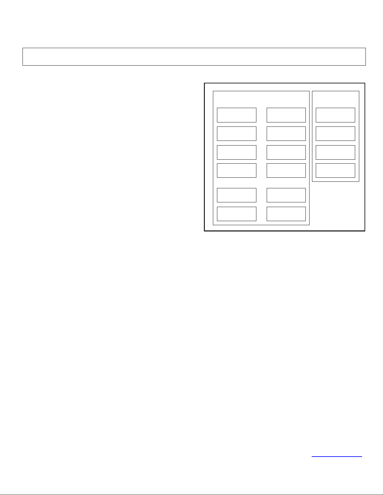
POWER ON
KEYPAD I/F
GPIO
LOGIC
BLOCK
DELAY 10mS
INTERRUPT
CONTROL
LDO CONTROL
ANALOG
BLOCK
BATTERY
CHARGER
REFERENCE
LDO1 to 11
APPLICATIONS
CDMA/CDMA2000/PCS Handsets
GENERAL DESCRIPTION
The ADP3500 is a multifunction power system chip optimized
for CDMA cell phone power management. It contains 15 LDOs.
Sophisticated controls are available for power up during battery
charging, keypad interface, GPIO/INT function and RTC
function. The battery charger has four modes as Pre-charge, Low
Current Charge, Full Current Charge, and Regulator modes, and
is designed for Li-Ion/Li-Polymer batteries.
SERIAL I/F
32KHz OUTPUT
CONTROL
RESET OUTPUT
Figure 1. Functional Block Diagram
RESET
RTC COUNTER
STAY-ALIVE
TIMER
VOLTAGE
DETECTOR
ADP3500
REV. PrP 2/6/02
Information furnished by Analog Devices is believed to be accurate and
reliable. However, no responsibility is assumed by Analog Devices for its
use, nor for any infringements of patents or other rights of third parties
which may result from its use. No license is granted by implication or
otherwise under any patent or apatent rights of Analog Devices.
One Technology Way, P.O. Box 9106, Norwood, MA 02062-9106, U.S.A.
Tel: 781/329-4700 World Wide Web Site: http://www.analog.com
Fax: 781/326-87ß3 ANALOG DEVICES, INC., 2002
Page 2
ADP3500 - SPECIFICATIONS
PRELIMINARY TECHNICAL DATA
MAIN FUNCTIONS
TA=-30 to +85°C, C
Parameter Symbol Conditions Min Typ Max Units
SHUTDOWN GND CURRENT
Power OFF
OPERATING GND CURRENT
Stand-by mode operation (light load)
Stand-by mode operation (Mid-load)
Active operation
Thermal Shutdown Threshold 160
Thermal Shutdown Hysteresis 35
Operational Temperature range Tope -30 +85
Adapter Voltage range (recommendation) VADP 5.5 12 V
VBAT Voltage range VBAT 3.3 5.5 V
=1µF MLCC, VBAT=3.6V unless otherwise noted. See Table 2 for C
VBAT
IGND
LDO3b : ON, connect to RTCV
through Schottky diode.
RTC/32K OSC : Active
AllotherLDOs:OFF
All logic inputs : VBAT or GND
MVBAT: OFF
IGND
LDO1b, 2b, 3b, 6b: ON
Io=1mA for LDO1b & 3b
Io=300µA for LDO2b & 6b
AllotherLDOs:OFF
RTC/32K OSC: Active
MVBAT: OFF
All logic output: no load
LDO1, 2, 3, 6, all Sub-LDO: ON,
Io=70% load
AllotherLDOs:OFF
RTC/32K OSC: Active
MVBAT: ON
All logic outputs: n o load
LDO5: OFF
All other LDOs: ON, 70% load
RTC/32K OSC: Active
All logic outputs: n o load
MVBAT: ON
OUT
.
25 40
60
275
650
125
µA
µA
µA
µA
°C
°C
°C
LDO SPECIFICATIONS
TA=25°C, C
Baseband VDD Main-LDO (LDO #1a)
Parameter Symbol Conditions Min Typ Max Units
OUTPUT VOLTAGE V
OUTPUT CAPACITOR REQUIRED FOR
STABILITY
DROPOUT VOLTAGE V
Start-up time from shutdown 250
GND Current I
Baseband VDD Sub-LDO (LDO #1b)
Parameter Symbol Conditions Min Typ Max Units
OUTPUT VOLTAGE V
GND Current I
REV.PrP 2/6/02 - 2 -
=1µF MLCC, VBAT = Vout+1V, NRCAP=0.1µF. See Table 2 for C
VBAT
LDO#1
C
LDO#1
DO
LDO#1
LDO#1b
LDO#1b
Io = 1 to 150 mA
Ta= -30 to +85°C
Io = 150 mA 200 mV
Io = 150 mA 50
Io = 1mA
Ta= -30 to +85°C
OUT
.
2.81 2.90 2.99 V
2.2
2.8 2.87 3.0 V
10
µF
µS
µA
µA
Page 3
ADP3500
PRELIMINARY TECHNICAL DATA
Baseband AVDD Main-LDO (LDO #2a)
Parameter Symbol Conditions Min Typ Max Units
OUTPUT Voltage V
OUTPUT default voltage V
OUTPUT Voltage V
LDO#2
LDO#2
LDO#2
16 steps, 20mV/step, Ta= 25C,
Io=50mA
Code : 1000
Code : 0111
Io=50mA,Ta=25°C
16 steps, 20mV/step, Io=50mA, Ta=
-30to+85°C
Code : 1000
Code : 0111
2.30
2.60
2.36
2.66
2.43
2.74VV
2.46 2.52 2.6 V
2.29
2.57
2.36
2.66
2.47
2.81VV
OUTPUT default voltage V
OUTPUT CAPACITOR REQUIRED FOR
C
LDO#2
LDO#2
Io=50mA,Ta=-30to+85°C
2.42 2.52 2.66 V
1
µF
STABILITY
DROPOUT VOLTAGE V
DO
Io = 50 mA 210 mV
RIPPLE REJECTION f = 1KHz 50 dB
OUTPUT NOISE VOLTAGE V
NOISE
Start-up time from shutdown 250
GND Current I
LDO#2
f = 100 Hz to 100 kHz 120
Io = 50 mA 50
µV
µS
µA
Baseband AVDD Sub-LDO (LDO #2b)
Parameter Symbol Conditions Min Typ Max Units
OUTPUT Voltage V
LDO#2b
Io = 300 µA, V
LDO#2a
=2.6V
2.50 2.70 V
Ta= -30 to +85°C
GND Current I
LDO#2b
5
µA
REFO switch
Parameter Symbol Conditions Min Typ Max Units
On resistance R
Off leak I
ON
LEAK
Ta= -30~+85°C, Io=500µA
LDO2: ON, Switch: OFF 0.01 1
50 130
Ω
µA
Coin Cell Main-LDO (LDO #3a)
Parameter Symbol Conditions Min Typ Max Units
OUTPUT VOLTAGE V
Dropout Voltage V
OUTPUT CAPACITOR REQUIRED FOR
C
LDO#3
DO
LDO#3
STABILITY
Start-up time from shutdown 250
GND Current I
LDO#3
Io = 1 to 50 mA
2.85 3.0 3.09 V
Ta= -30 to +85°C
Io= 50 mA 140 mV
1
µF
µS
Io = 50 mA 50
µA
RMS
Coin Cell Sub-LDO (LDO #3b)
Parameter Symbol Conditions Min Typ Max Units
OUTPUT VOLTAGE V
LDO#3b
Io=1mA
2.85 2.97 3.15 V
Ta= -30 to +85°C
GND Current I
LDO#3b
10
µA
Audio LDO (LDO #4)
Parameter Symbol Conditions Min Typ Max Units
OUTPUT VOLTAGE V
LDO#4
Io = 1 to 180 mA
2.81 2.90 2.99 V
Ta=-30to+85°C
OUTPUT CAPACITOR REQUIRED FOR
C
LDO#4
2.2
µF
STABILITY
Dropout Voltage V
DO
Io = 180 mA 200 mV
RIPPLE REJECTION f = 1KHz 50 dB
OUTPUT NOISE VOLTAGE V
NOISE
Start-up time from shutdown 250
GND Current I
LDO#4
f = 100 Hz to 10 kHz 50
Io = 180 mA 50
µV
µS
µA
REV.PrP 2/6/02 - 3 -
RMS
Page 4
ADP3500
PRELIMINARY TECHNICAL DATA
Vibrator LDO (LDO #5)
Parameter Symbol Conditions Min Typ Max Units
Output Voltage V
Dropout Voltage V
Output capacitor required for stability C
GND Current I
LDO#5
DO
LDO#5
LDO#5
Baseband Core Main-LDO (LDO #6a)
Parameter Symbol Conditions Min Typ Max Units
Output Voltage V
Output capacitor required for stability C
Dropout Voltage V
LDO#6
LDO#6
DO
Start-up time from shutdown 250
GND Current I
LDO#6
Baseband Core Sub-LDO (LDO #6b)
Parameter Symbol Conditions Min Typ Max Units
OUTPUT VOLTAGE V
GND Current I
LDO#6b
LDO#6b
RF Rx1 LDO (LDO #7)
Parameter Symbol Conditions Min Typ Max Units
Output voltage V
Output capacitor required for stability C
Dropout voltage V
Ripple rejection f = 1KHz 50 dB
Output noise voltage V
Start-up time from shutdown 250
GND Current I
LDO#7
LDO#7
DO
NOISE
LDO#7
Io = 1 to 150 mA
2.75 2.9 3.05 V
Ta= -30 to +85°C
Io = 150mA 200 mV
2.2
Io = 150 mA 50
Io = 1 to 50 mA
2.52 2.60 2.68 V
µF
µA
Ta= -30 to +85°C
1
µF
Io = 50 mA 160 mV
µS
Io = 50 mA 50
Io = 300 µA
2.5 2.57 2.7 V
µA
Ta= -30 to +85°C
Io = 1 to 100 mA
5
2.81 2.9 2.99 V
µA
Ta= -30 to +85°C
1.5
µF
Io = 100 mA 200 mV
f = 100 Hz to 100KHz 40
µV
µS
Io=100mA 50
µA
RMS
RF Tx LDO (LDO #8)
Parameter Symbol Conditions Min Typ Max Units
Output voltage V
LDO#8
Io = 1 to 150 mA
2.81 2.9 2.99 V
Ta= -30 to +85°C
Output capacitor required for stability C
Dropout voltage V
LDO#8
DO
Io = 150mA 200 mV
2.2
µF
Ripple Rejection f = 1KHz 50 dB
Output noise voltage V
NOISE
Start-up time from shutdown 250
GND Current I
LDO#8
f = 100 Hz to 100KHz 40
Io=150mA 50
µV
µS
µA
RF Rx 2 LDO (LDO #9)
Parameter Symbol Conditions Min Typ Max Units
Output voltage V
LDO#9
Io = 1 to 50 mA
2.81 2.9 2.99 V
Ta= -30 to +85°C
Output capacitor required for stability C
Dropout voltage V
LDO#9
DO
Io = 50mA 150 mV
1
µF
Ripple Rejection f = 1KHz 50 dB
Output noise voltage V
NOISE
Start-up time from shutdown 250
GND Current I
LDO#9
f = 100 Hz to 100KHz 40
Io=50mA 50
µV
µS
µA
RF Optional LDO (LDO #10)
Parameter Symbol Conditions Min Typ Max Units
Output voltage V
LDO#10
Io= 1 to 50 mA
Ta= -30 to +85°C
2.81 2.9 2.99 V
RMS
RMS
REV.PrP 2/6/02 - 4 -
Page 5
ADP3500
PRELIMINARY TECHNICAL DATA
Output capacitor required for stability C
Dropout voltage V
LDO#10
DO
Io = 50mA 150 mV
Ripple rejection f = 1KHz 50 dB
Output noise voltage V
NOISE
f = 100 Hz to 100KHz 40
Start-up Time from Shutdown 250
GND Current I
LDO#10
Io=50mA 50
Optional LDO (LDO #11)
Parameter Symbol Conditions Min Typ Max Units
Output voltage V
LDO#11
Io = 1 to 100 mA
Ta= -30 to +85°C
Output capacitor required for stability C
LDO#11
Ripple rejection f = 1KHz 50 dB
Output noise voltage V
NOISE
f = 100 Hz to 100KHz 50
Start-up Time from Shutdown 250
GND Current I
LDO#11
Io=150mA 50
Voltage Detector for LDO1 and LDO6
Parameter Symbol Conditions Min Typ Max Units
LDO1 detect voltage V
LDO1 release voltage V
LDO1 Hysteresis V
LDO6 detect voltage V
LDO6 release voltage V
LDO6 Hysteresis V
DET1
DET1
HYS1
DET6
DET6
HYS6
Ta= -30 to +85°C
Ta= -30 to +85°C
Ta= -30 to +85°C
Ta= -30 to +85°C
Ta= -30 to +85°C
Ta= -30 to +85°C
1
1.42 1.5 1.58 V
2.2
2.7 2.72 V
2.77 V
LDO1
-NOM
35 52 85 mV
2.3 2.33 V
2.40 V
LDO6
-NOM
40 60 100 mV
µF
µV
µS
µA
µF
µV
µS
µA
V
V
RMS
RMS
BATTERY VOLTAGE DIVIDER: MVBAT
TA=-30 to 85°C, C
Parameter Symbol Conditions Min Typ Max Units
MVBAT Output voltage
5 – bit programmable V
MVBAT Output voltage step Vstep VBAT=4.35V, MVEN = 1 6 mV/lsb
Output drive current capability Iout 1 2 mA
MVBAT Load Regulation
MVBAT Output Voltage Step VBAT = 4.35 V, MVEN = 1 6 mV
Operating Battery Current VBAT = 4.35 V, MVEN = 1 65 85
Shutdown Current VBAT = 4.35 V, MVEN = 0 1
=10µF MLCC, C
VBAT
=1µFMLCC
Adapter
unless otherwise noted
VBAT=4.35V, MVEN = 1
MVBAT
∆ΜVBAT 0 < Iout < 100 µA
code 10000
code 01111
2.484
2.673
2.508
2.697
2.533
2.727
V/V
V/V
35mV
µA
µA
BATTERY CHARGER
TA=-30 to 85°C, C
Parameter Symbol Conditions Min Typ Max Units
Charger Control Voltage Range
2 – bit programmable
Charger Control Voltage Range
2 – bit programmable
=10µF MLCC, C
VBAT
=1µF MLCC, 4.0V ≤ ADAPTER ≤ 12V
Adapter
VBAT
SENSE
Ta= 25 °C,
V
R_SENSE
5.5V ≤ ADAPTER ≤ 12V (note 1)
code 00 (default)
code 01
code 10
code 11
VBAT
SENSE
Ta= -20 to 55°C,
V
R_SENSE
5.5V ≤ ADAPTER ≤ 12V (note 1)
code 00 (default)
code 01
code 10
code 11
unless otherwise noted
= 6mV & 115mV,
= 6mV & 115mV,
3.926
4.150
4.170
4.190
3.905
4.130
4.146
4.166
3.980
4.190
4.210
4.230
3.980
4.190
4.210
4.230
4.034
4.230
4.250
4.270
4.065
4.250
4.278
4.300
V
V
V
V
V
V
V
V
REV.PrP 2/6/02 - 5 -
Page 6
ADP3500
PRELIMINARY TECHNICAL DATA
Charger Detect On Threshold ADAPT
ERVBAT
Charger Detect Off Threshold ADAPT
ER-
VBAT
Charger Supply Current I
Current Limit Threshold
High Current Limit
(Full charge current enabled)
Low Current Limit
(Full charge current disabled)
Pre-Charge Current Source
Base Pin Drive Current Note 2. 15 28 mA
Deep Discharge Lock-Out (Releasing voltage) DDLO VBAT<DDLO, Ta=25C, 5mA Pre-
Deep Discharge Lock-Out Hysteresis 200 mV
ISENSE Bias Current I
BATID pull-up resistor to ADAPTER R
Minimum Load for Stability I
ADAPTER
ADAPT
ER-V
ISNS
BATID
L
ADAPTER=5V,VBAT=4.3V 2 mA
ADAPTER=5V
VBAT=3.6V
ISNS
VBAT=3.0 V
VBAT ≤ DDLO
charge, VBAT ramping up
V
=5V 1
ISNS
BATID=H. Note 3. 10 mA
Note 1: Overhead includes external components, including sense resistor, PNP and isolation diode.
2: DDLO hysteresis is dependent upon DDLO threshold value. If DDLO threshold is at maximum, DDLO hysteresis is at
maximum at the same time.
3: Guaranteed but not tested.
110 165 225 mV
52350mV
135401605518570mV
mV
357mA
2.675 2.78 V
µA
70 100 130
KΩ
REV.PrP 2/6/02 - 6 -
Page 7

ADP3500
PRELIMINARY TECHNICAL DATA
LOGICS
DC Specifications
TA=25°C, C
Parameter Symbol Conditions Min Typ Max Units
CS, CLKIN, RESETIN-, TCXO_ON, SLEEP-,
KEYPADROW (Internal 10KΩ pull-up)
Input High Voltage
Input Low Voltage
Hysteresis
GPIO, DATA
Input High Voltage
Input Low Voltage
Hysteresis
Output High Voltage
Output Low Voltage
INT-
Output High Voltage
Output Low Voltage
BLIGHT (Open Drain Output)
Output Low Voltage
KEYPADCOL (Open Drain Output)
Output Low Voltage
PWRONKEY-, OPT1 (Internal 140KΩ Pull-up)
Input High Voltage
Input Low Voltage
Hysteresis
OPT2- (Input/Open Drain Output)
Input High Voltage
Input Low Voltage
Hysteresis
Output Low Voltage
OPT3
Input High Voltage
Input Low Voltage
Hysteresis
32KOUT
Output High Voltage
Output Low Voltage
RESET+ (Open Drain Output)
Output Low Voltage
OFF Leak
RSTDELAY-, RESETOUT- (Open Drain Output)
Output Low Voltage
BATID (Internal 100KΩ pull-up)
Input High Voltage
Input Low Voltage
Hysteresis
Supply Current of RTCV I
VADP: Adapter voltage
=1µF MLCC, VBAT = 3.6 V
VBAT
VIH
VIL
VIH
VIL
VOH
VOL
VOH
VOL
VOL
VOL
VIH
VIL
Vhys
VIH
VIL
Vhys
VOL
VIH
VIL
Vhys
VOH
VOL
VOL
OFF
VOL
VIH
VIL
OSC
IOH=400µA
IOL=-1.8mA
IOH=400µA
IOL=-1.8mA
IOL=-100mA
IOL=-1.8mA
IOL=-1.8mA
IOH=400µA
IOL=-1.8mA
IOL=-1.8mA
LEAK
IOL=-1.8mA
VADP=5 to 12V 0.8xVADP
RTCV=3V,
VBAT=0V
All logic: No load.
2.25
2.25
2.69
2.69
0.8xVBAT
0.8xVBAT
0.7xVBAT
0.9xRTCV
470
470
950
950
300
0.005
0.16 x
VADP
1
0.5
0.5
0.28
0.28
0.4
0.15
0.2xVBAT
0.2xVBAT
0.1xVBAT
0.2xVBAT
0.1xRTCVVV
0.1xRTCV
1
0.1xRTCV
0.2xVADPVV
V
V
mV
V
V
V
mV
V
V
V
V
V
V
V
V
mV
V
V
mV
V
V
V
mV
V
µA
V
V
µA
AC Specifications
All specs include temperature unless otherwise noted
Parameter Symbol Conditions Min Typ Max Units
Operational Supply Range RTCV 2 3.1* V
Oscillator Frequency F
Start-up Time (note) t
Frequency deviation f
REV.PrP 2/6/02 - 7 -
CLK
START
DEV
RTCV=0V to 3V 100 200 mS
RTCV=2 to 3V TBD
32.768 KHz
Page 8
ADP3500
PRELIMINARY TECHNICAL DATA
Frequency Jitter
Cycle to Cycle
>100cycles
Long term Drift RTCV=3V, 3 minutes 10* ppm
SERIAL INTERFACE
Parameter Min. Typ. Max Units Test Condition/Comments
t
t
t
t
t
t
t
t
t
t
t
CKS
CSS
CKH
CKL
CSH
CSR
DS
DH
RD
RZ
CSZ
50 nS CLK set-up time
50 nS CS set-up time
100 nS CLK “High” Duration
100 nS CLK “Low” Duration
100 nS CS hold time
62
µS
50 nS Input data set-up time
40 nS Input data hold time
50 nS Data output delay time
50 nS Data output floating time
50 nS Data output floating time after CS goes low.
Note: These parameters are not tested.
ABSOLUTE MAXIMUM RATINGS
Voltage on ADAPTER pin to GND ……………………………..... -0.3, 15Vmax
Voltage on VBAT pin to GND …………………………………… -0.3, 7Vmax
Voltage on Pin 6-13, 21-28 to GND ……………………………… -0.3, V
Voltage on Pin 1, 62-64 ………………………………………….. - 0.3, VBAT+0.3V max
Voltage on Pin 20, 32 …………………………………………….. - 0.3, V
Voltage on Pin 60, 61 ……………………………………………... - 0.3, V
Voltage on Pin 2-5, 14, 30, 31, 33 …………………………………. - 0.3, 7V max
Storage Temperature Range ………………………………………. - 65 to +150 °C
Operating Temperature Range ……………………………………. - 30 to +85°C
Maximum Junction Temperature …………………………………. 125°C
Thermal Impedance (LQFP-64) ………………………………. 2 layer bo ard 76°C/W
θ
JA
θ
Thermal Impedance (LQFP-64) ………………………………. 4 layer bo ard 54°C/W
JA
Lead Temperature Range (Soldering, 60 sec) ……………………... 300°C
/S
f
JITTER
EC
CS recovery time
RTCV=3V, TA=25°C
+0.3Vmax
LDO1
+0.3V max
RTCV
ADAPTER
40*
50*
+0.3V max
nS
nS
ORDERING GUIDE
Model Temperature Range Package
ADP3500AST -30 C to 85 C LQFP 64 pins
REV.PrP 2/6/02 - 8 -
Page 9
ADP3500
:
PRELIMINARY TECHNICAL DATA
PIN CONFIGURATION
R
E
E
2
T
P
O
T
S
D
P
E
I
N
A
T
S
E
A
A
D
W
S
B
B
I
A
P
64 49
1
OPT3
KEYPADCOL0
KEYPADCOL1
KEYPADCOL2
KEYPADCOL3
KEYPADROW0
KEYPADROW1
KEYPADROW2
KEYPADROW3
KEYPADROW4
KEYPADROW5
TCXO_ON
SLEEPBLIGHT
DGND
INT-
16
17
0
1
V
C
T
R
2
D
O
O
O
N
I
I
I
C
G
P
P
P
S
A
G
G
G
O
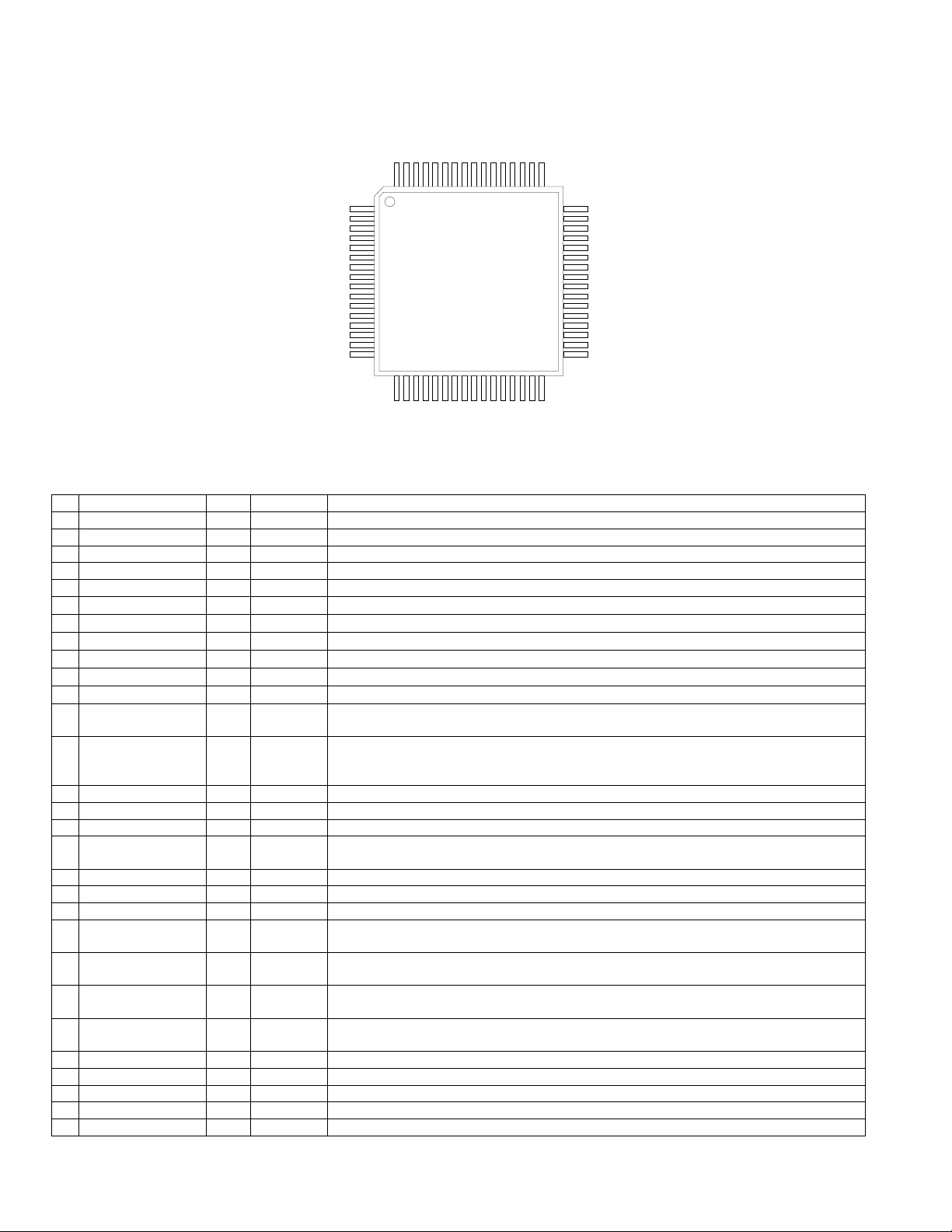
Figure 2. Pin Configuration
PIN DESCRIPTION
Pin Mnemonic I/O Supply Function
1 OPT3 I VBAT Optional Power ON input. ADP3500 will keep “power ON” during this pin goes “High”.
2 KEYPADCOL0 O LDO1 Keypad Column Strobe 0 (Open Drain, pull low)
3 KEYPADCOL1 O LDO1 Keypad Column Strobe 1 (Open Drain, pull low)
4 KEYPADCOL2 O LDO1 Keypad Column Strobe 2 (Open Drain, pull low)
5 KEYPADCOL3 O LDO1 Keypad Column Strobe 3 (Open Drain, pull low)
6 KEYPADROW0 I LDO1
7 KEYPADROW1 I LDO1
8 KEYPADROW2 I LDO1
9 KEYPADROW3 I LDO1
10 KEYPADROW4 I LDO1
11 KEYPADROW5 I LDO1
12 TCXO_ON I LDO1 Logic input pin for Main LDOs (LDO1, LDO2, LDO3, LDO6) turning on control. L: OFF, H
13 SLEEP- I LDO1 Logic input pin for RF Rx LDOs (LDO7 and LDO9). Gatingregister data with this input for
14 BLIGHT O VBAT LEDdrive. Open drain output.
15 DGND - - Digital Ground
16 INT- O LDO1 Interrupt signal output
17 RTCV - - Supply input for RTC, 32KHz OSC, and some other logics. Connects to Coin cell battery in
18 OSCOUT - RTCV Connect to 32.768KHz crystal.
19 AGND - - Analog Ground
20 OSCIN - RTCV Connect to 32.768KHz crystal.
21 GPIO0 I/O LDO1 General Purpose Input and Output port. Integrated Interrupt function. Interrupt occurs both
22 GPIO1 I/O LDO1 General Purpose Input and Output port. Integrated Interrupt function. Interrupt occurs both
23 GPIO2 I/O LDO1 General Purpose Input and Output port. Integrated Interrupt function. Interrupt occurs both
24 GPIO3 I/O LDO1 General Purpose Input and Output port. Integrated Interrupt function. Interrupt occurs both
25 DATA I/O LDO1 Serial Interface data input and output.
26 CS I LDO1 Serial Interface Chip Select input. ActiveHigh input.
27 CLKIN I LDO1 Serial Interface Clock input.
28 RESETIN- I LDO1 Reset input signal for internal reset signal and starts Stay-Alive timer.
29 32KOUT O RTCV 32.768KHz output. Output after 30mS when Reset is released.
Keypad Row Input 0. Pulled up internally, 10KΩ
Keypad Row Input 1. Pulled up internally, 10KΩ
Keypad Row Input 2. Pulled up internally, 10KΩ
Keypad Row Input 3. Pulled up internally, 10KΩ
Keypad Row Input 4. Pulled up internally, 10KΩ
Keypad Row Input 5. Pulled up internally, 10KΩ
ON
these LDOs. LDO7 and LDO9 are turned OFF when SLEEP- goes Low even if the registers
set to ON.
typical operation.
falling and raising edge.
falling and raising edge.
falling and raising edge.
falling and raising edge.
)
n
o
i
t
)
p
2
)
x
x
O
T
R
F
F
F
R
(
R
R
(
(
P
T
0
A
D
A
B
N
C
V
R
G
N
M
A
D
1
9
8
T
N
S
A
O
O
V
B
O
G
B
D
D
D
A
V
L
L
L
48
VBAT
LDO7 (RF Rx1)
LDO6 (Baseband Core)
VBAT
LDO5 (Vibrator)
LDO4 (Audio)
VBAT
LDO2 (Baseband AVDD)
REFO
AGND
LDO3 (RT C/Coin-cell)
VBAT
LDO1 (Baseband VDD)
LDO11 (Option)
VBAT
RSTDELAY-
33
32
3
T
O
I
A
P
D
G
+
S
N
I
C
K
L
C
T
T
N
T
S
I
U
E
E
T
O
S
T
E
T
E
S
E
R
E
S
R
E
R
-
-
A
REV.PrP 2/6/02 - 9 -
Page 10

ADP3500
PRELIMINARY TECHNICAL DATA
30 RESET+ O RTCV Reset output. Invert signal of RESETOUT-. Open drain and low OFF leak.
31 RESETOUT- O RTCV Reset output. FollowsVoltage Detector operation. Open drain output.
32 TEST I RTCV Test pin. If the pin tied to RTCV, test mode runs. Connect to GND for normal operation.
33 RSTDELAY- O RTCV Reset output. 50mS delayed. Connect to baseband’ reset input as typical application. Open
drain output.
34 VBAT - - Supply input. Connect to Battery.
35 LDO11 O VBAT Regulator #11 output. Use for Optional circuit.
36 LDO1 O VBAT Regulator #1 output. Use for Baseband I/O supply.
37 VBAT - - Supply input. Connect to Battery.
38 LDO3 O VBAT Regulator #3 output. If VBAT>2.7V, the output is always active. Use for Coin cell supply.
39 AGND - - Analog Ground
40 REFO O VBAT Output of LDO2 through FET switch.
41 LDO2 O VBAT Regulator #2 output. Use for Baseband analog supply.
42 VBAT - - Supply input. Connect to Battery.
43 LDO4 O VBAT Regulator #4 output. Use for General analog supplies. Ex. Speaker Amp.
44 LDO5 O VBAT Regulator #5 output. Use for Vibrator.
45 VBAT - - Supply input. Connect to Battery.
46 LDO6 O VBAT Regulator #6 output. Use for Baseband core supply.
47 LDO7 O VBAT Regulator #7 output. Use for RF Rx IC supply. Gated with SLEEP- signal input.
48 VBAT - - Supply input. Connect to Battery.
49 LDO8 O VBAT Regulator #8 output. Use for RF Tx IC supply.
50 AGND - - Analog Ground
51 LDO9 O VBAT Regulator #9 output. Use for RF Rx IC supply. Gated with SLEEP- input signal.
52 VBAT - - Supply input. Connect to Battery.
53 LDO10 O VBAT Regulator #10 output. Use for Optional circuit.
54 BVS - - Battery Voltage Sense input for Charger. Connect to Battery.
55 NRCAP O VBAT
56 AGND - - Analog Ground
57 MVBAT O VBAT Battery voltage divider output. Buffered internally. Connect to Baseband ADC.
58 BASE O ADAPTER Base drive output for PNP pass transistor
59 ADAPTER - - AC adapter input. Use to charger supply.
60 BATID I ADAPTER
61 ISENSE I ADAPTER Charge current sense input
62 PWRONKEY- I VBAT
63 OPT1- I VBAT Optional Power ON input. ADP3500 will keep “power ON” during this pin goes “Low”.
64 OPT2- I/O VBAT Optional Power ON input. ADP3500 will keep “power ON” during this pin goes “Low”.
Noise reduction capacitor. 0.1µF MLCC.
Battery identification. 100KΩ pulled up internally. “L”: Battery exist, “H”: No battery. If
BATID=”H”, Charger operates with “No current Limit”.
Power ON/OFF key input. Pulled up internally (140KΩ).
While the part is powered up, the input is pulled to Low (GND) internally. Don’t connect to
any supply or signal source.
REV.PrP 2/6/02 - 10 -
Page 11

BLOCK DIAGRAM
PRELIMINARY TECHNICAL DATA
ADP3500
PWRO NKEY-
OPT1OPT2-
OPT3
INT-
KEYPADCOL0
KEYPADCOL1
KEYPADCOL2
KEYPADCOL3
KEYPADROW0
KEYPADROW1
KEYPADROW2
KEYPADROW3
KEYPADROW4
KEYPADROW5
BLIGHT
DGND
CS
CLKIN
DATA
GPIO0
GPIO1
GPIO2
GPIO3
OSC IN
OSC OUT
32K OUT
62
63
64
1
16
2
3
4
5
6
7
8
9
10
11
14
15
26
27
25
21
22
23
24
20
18
29
POWERON_N
OPT1_N
OPT2_N
OPT3
Level
trans
Level
trans
4
Level
trans
6
LDO1
Level
trans
32KHz
RTC
/clock
Stay/Alive
Timer
0.25-8sec
Alarm
CLK
LDO1
KEY
PAD
RTC
I/F
140K
VBAT
Ω
sync
CLKs
Data
Data
RESETIN_N
AGND
Delay
10mS
5
Data
In
5
INT
GPIO_INT/ gpi_intrst
Serial
I/F
GPIO
+
INT
Level Translator
Delay
30mS
power_on
voltage_detect
PWROFF
INT_N
DATA
DATA
CLK
BATID
CLKs
VBAT
Charger_Detect
ChargerControl
ADAPTER ISENSE
ON/OFF
LOGIC
ON/OFF
LOGIC
ON/OFF
LOGIC
ON/OFF
LOGIC
Level Translator
DGND
VBAT & RTCV
Delay
50mS
DGND
Ω
100K
Battery Charger
DDLO
LDO_EN
Main
Sub
Main
Sub
Main
Main
Sub
REF
LDO1
LDO2
LDO3
LDO6
LDO4
LDO5
LDO7
LDO8
LDO9
LDO10
LDO11
Voltage
Detector
LDO1
RTCV
Open Drain
BASE
REF
LPF
RTCV
BVS
5458615934374245485219395056
Level
trans
LDO1
60
BATID
57
MVBAT (VBAT Measure)
40
REFO
55
NRCAP
LDO1
36
LDO1 (Baseband VDD)
41
LDO2 (Baseband AVDD)
38
LDO3 (RTC/Coin-cell)
46
LDO6 (Baseband Core)
43
LDO4 (Audio)
44
LDO5 (Vibrator)
47
LDO7 (RF Rx1)
49
LDO8 (RFTx)
51
LDO9 (RFRx2)
53
LDO10 (RF Op tion)
35
LDO11 (Option)
13
SLEEP-
12
TCXO_ON
28
RESETIN-
17
RTCV
32
TEST
33
RSTDELAY-
31
RESETOUT-
30
RESET+
Figure 3. Overall Block Diagram
REV.PrP 2/6/02 - 11 -
Page 12

ADP3500
PRELIMINARY TECHNICAL DATA
Theory of Operations
As illustrated in Figure 1 at the beginning, ADP3500 can be divided into two high level blocks – Analog and Logic.TheAnalog
block mainly consists of LDO regulators, battery charger, reference voltage, and voltage detector sub-blocks, all of which are
powered by the main power source(VBAT), namely the main battery or the charging adapter. On the other hand, the Logic block is
more complicated. All the Logic sub-blocks are also powered by VBAT except the RTC counter, 32MHz Output control, RESET
Output, and Stay-Alive T i mer. These sub-blocks are powered from RTCV pin, as indicated in Figure 4 in shaded area.
[VBAT]
5
POWER ON
DELAY 10mS6
4
3
2
1
[RTCV]- RTC BLOCK
10
KEYPAD I/F
GPIO
SERIAL I/F
RESET
32K OUTPUT
CONTROL
RESET OUTPUT
Figure 4. Power partitioning of sub-blocks
7
8
9
11
INTERRUPT
LDO CONTROL
RTC COUNTER
STAY-ALIVE TIMER
CONTROL
ANALOG
BLOCK
1. ANALOG BLOCKS
1.1 LOW DROP-OUT(LDO) REGULATORS
There are total four Sub-LDOs for each LDO1, 2, 3, and 6, in order to meet lower power consumption at light load (stand-by
operation). They are used at low load condition, but they are continuously ON even if the each Main-LDOs are ON. The LDO3 and
3b are used for Coin cell and LDO3b is always ON until Main battery (VBAT) is downed to 2.5V due to DDLO function. LDO7 and
9 are controlled with SLEEP- signal. For detail of LDO ON/OFF control, please refer to Section “2.8 LDO Control”.
Table 1. Ground currents of LDOs with each handset operations.
LDO names
LDO # 1 6 3 4 5 2 7 8 9 10 11
Power OFF
Light load
Stand-
by
Mid-load
mode
Active load
Talk
Ring
REV.PrP 2/6/02 - 12 -
Baseband
VDD
OFF OFF
10µA5µA10µA
60µA55µA60µA
60µA55µA60µA
60µA55µA60µA50µA
60µA55µA60µA50µA50µA55µA50µA50µA50µA50µA50µA20µA 600µA
Baseband
Core
Coin Cell Audio Vibrator
10µA
OFF OFF OFF OFF OFF OFF OFF OFF
OFF OFF
OFF OFF
OFF OFF
OFF
Baseband
AVDDRFRx1RFTxRFRx2RFOption
5µA
55µA
55µA50µA50µA50µA50µA
55µA50µA50µA50µA50µA50µA20µA 550µA
OFF OFF OFF OFF OFF
OFF OFF OFF
50µA
Option
OFF
OFF
Main
Total LDO
REF
20µA30µA
20µA50µA
20µA 300µA
20µA 450µA
IGND
Page 13

Table 2. LDO operation overview
PRELIMINARY TECHNICAL DATA
Regulator Names
Current
Rating (mA)
Voltage (Typ)
Or Range
Program steps
Step size
(mV)
Default Cout
LDO1a B aseband VDD 150 2.90V N/A N/A LDO1b Baseband VDD sub 1 2.87V N/A N/A LDO2a Baseband AVDD 50 2.36V~2.66V 16 20 2.52V
LDO2b Baseband AVDD sub 0.3 2.33V~2.63V 16 20 2.49V
LDO3a RTC/Coin Cell 50 3.0V N/A N/A LDO3b RTC/Coin Cell sub 1 2.97V N/A N/A LDO4 Audio 180 2.9V N/A N/A LDO5 Vibrator 150 2.9V N/A N/A LDO6a Baseband Core 50 2.6V N/A N/A LDO6b Baseband Core sub 0.3 2.57V N/ A N/A LDO7 RF Rx1 100 2.9V N/A N/A LDO8 RF Tx 150 2.9V N/A N/A LDO9 RF Rx2 50 2.9V N/A N/A LDO10 RF Option 50 2.9V N/A N/A LDO11 Option 100 1.5V N/A N/A -
1.2 BATTERY CHARGER
1.2.1. Block Diagram
ADP3500
2.2µF
2.2µF
1µF
1µF
1µF
1µF
2.2µF
2.2µF
1µF
1µF
2.2µF
2.2µF
1µF
1µF
2.2µF
AC Adapter
BATID
100KΩ
BATID
C
ADAPTER
BVS
ADAPTER
REF
V(ISENSE)
DDLO
EN
RSENSE
ISENSE
Pre-charge
5m A
+
-
CHI
LDO_
EN
CHEN
gm
EN
LOGIC Block
Figure 5. Battery charger block diagram
BASE
gm
EN
Charger_
Detect
BVS
MVBAT
CHV
MVEN MV4:0
0/1
Cvbat
VBAT
Battery
EN
MVBAT
REV.PrP 2/6/02 - 13 -
Page 14

1.2.2. Flow Chart
PRELIMINARY TECHNICAL DATA
ADP3500
Batterychargerstart
DDLO comparator will
operate i f VBAT>2V.
Even if VBAT<2V, precharge is continuously
applying 5mA.
RESETIN- should be
asserted until baseband
chip active.
Then, CHEN=1 as default.
BATID=0: Batteryconnected
BATID=1: Batterydisconnected
Determined by external
sense resistor
V
Set Charger Detect flag
>VBAT
ADAPTER
?
Y
VBAT>DDLO
?
LDO3b: ON
BATID=0
?
Set Low Current Charge
I
=250mA
ADAPTER
(50mV on Rsense)
Pre-charge: OFF
N
Pre-charge 5mA
Current Loop Disabled
Voltage Loop Regulates
VBAT to 4.0V
Pre-charge:OFF
LDO1,1b,2,2b,3,6,6b
Voltage Detector
all enabled
Voltage Detector
VLDO6>2.5V
AND
VLDO1>2.7V
?
Figure 6. Charger flow chart A
REV.PrP 2/6/02 - 14 -
Page 15

A
PRELIMINARY TECHNICAL DATA
Reset sequence runs
Baseband sets Charge Voltage
Baseband sets MVBAT gain
ADP3500
CHI=0: Full current charge OFF
CHI=1: Full current charge ON
Figure 7. Charger flow chart B
1.2.3. Charger Detect function
The ADP3500 will detect that a charging adapter has been applied when the voltage at the ADAPTER pin exceeds the voltage at
BATSNS. The ADAPTER pin voltage must exceed the BVS voltage by a small positive offset. This offset has hysteresis to prevent
jitter at the detection threshold. The charger detection comparator will set the Charger_Detect flag in the 20h register and generate an
interrupt to the system. If the ADAPTER input voltage drops below the detection threshold, charging will stop automatically and the
Charger_Detect flag will be cleared and generate an interrupt also.
BasebandEnables
Full charge current?
(CHI=1?)
Y
Low Current Charge: OFF
SetFullcurrentcharge
I
ADAPTER
(150mV on Rsense)
N
Charging Terminated
=750mA
Baseband
CHEN=0?
Y
N
1.2.4. DDLO function and operation
The ADP3500 contains a comparator that will lock out system operation if the battery voltage drops to the point of deep discharge.
When the battery voltage exceeds 2.675 V, the reference will start as will the sub-LDO 3b. If the battery voltage drops below the
hysteresis level, the reference and LDO's will be shut down, if for some reason they are still active. Since LDO1 will be in deep
dropout and well below the voltage detector threshold at this point, the reset generator will have alread y shut down the rest of the
system via RESET+, RESETOUT-, and RSTDELAY-.
If a charging adapter has been applied to the system, the DDLO comparator will force the charging current to trickle charge if the
battery is below the DDLO thr eshold. During this time, the charging current is limited to 5 mA. When the battery voltage exceeds
the upper threshold, the low current charging is enabled, which allows 55 mV (typical) across the external charge current sense
resistor. See also Figure 6, the Battery Charger Flowchart.
1.3 MVBAT
The ADP3500 provides a scaled buffered output voltage for use in reading the battery voltage with an A/D converter. The battery
voltage is divided down to be nominally 2.600 V at full scale battery of 4.35 V. To assist with calibrating o ut s ystem errors in the
REV.PrP 2/6/02 - 15 -
Page 16

ADP3500
PRELIMINARY TECHNICAL DATA
ADP3500 and the external A/D converter, this full scale voltage may be trimmed digitally with 5 bits stored in register 12h. At full
scale input voltage, the output voltage of MVBAT can be scaled in 6 mV steps, allowing a very fine calibration of the battery voltage
measurement. The MVBAT buffer is enabled by the MVEN bit of register 11h, and will consume less than 1 uA of leakage current
when disabled.
1.4 REFERENCE
The ADP3500 has an internal, temperature compensated and trimmed band-gap reference. The battery charger and LDO's all use
this system reference. This reference is not available for use externally. However, to reduce thermal noise in the LDOs, the
reference voltage is brought out to the NRCAP pin through a 50kohm internal resistor. A cap on the NRCAP pin will complete a low
pass filter that will reduce the noise on the reference voltage. All the LDO's, with the exception of LDO3, use the filtered reference.
Since the reference voltage appears at NRCAP through a 50kohm series internal impedance, it is very important to never place any
load current on this pin. Even a volt meter with 10 megohm input impedance will affect the resulting reference voltage by about 6 or
7 mV, affecting the accuracy of the LDO's and charger. If for some reason the reference must be measured, be certain to use a high
impedance range on the volt meter or a discrete high impedance buffer prior to the measurement system.
2. LOGIC BLOCKS
ADP3500 has following logic functions.
• Three wire Serial Interface (CS, C LK, DATA)
• RTC counter section has Year, Month, Day, W eek,
Hour, Minute, and Second, and controls Leap year,
and days in month automatically.
• Detect Alarms based on RTC counter.
• Periodically constant interrupt feature. (2Hz, 1Hz,
1/60Hz, 1/3600Hz, Once a months)
• GPIO and INT ports control
• Key-pad interface
• LED light control
• LDO functions
• Clock a nd Reset output control
• Stay-Alive timer
Following is a block diagram based on Logic circuit.
REV.PrP 2/6/02 - 16 -
Page 17

PWRONKEY_N
PRELIMINARY TECHNICAL DATA
OPT1_N
OPT2_N
OPT3
BLIGHT
DGND
KEYPADCOL
KEYPADROW
GPIO[3:0]
INT_N
TCXO_ON
SLEEP_N
CLKIN
DATA
RESETIN_N
OSCOUT
OSCIN
32K OUT
RESETOUT_N
RSTDELAY_N
RESET
TEST
ADP3500
[VBAT]
batid
voltage_detect
chager_detect
Analog
Blocks
t
SYNC.
DELAY
10mS
POWER
OFF
DATA
IN
INT
control
register
(reset & mask)
clk32k
clk1k
test_ldoenable
test_mode
SYNC.
LDO control register
Analog
control
registers
LDO
Control
rtc_voltage_detect
voltage detect_delay
power_on
Interrupt
register
pwronkey_n_sync,
opt1_n_sync,
opt3_sync
SYNC.
Analog block
BL
LED control
4
6
4
CS
Serial
I/F
resetin_n
(reset for registers)
rtc_resetin_n
analog block
32K OSC
32K CLK
output
control
write_enable
write_data[7:0]
sp_addr[4:0]
rtc_clk32k
clk512
Test mode
register
block
reset output
control
KEY PAD
I/F
GPIO
Data
select
block
KEY PAD
I/F control
keypad_int
GPIO
control
t
n
i
_
m
r
a
l
t
a
t
r
Output data
select
Address
decode
RTC register block
rtc_voltage_detect
c
S
C
_
C
T
R
RTC
t
n
o
c
Stay-Alive
e
d
Timer
o
m
t
s
e
T
rtc_test
[RTCV]
Figure 8. LOGIC block diagram
2.1 RESET
2.1.1 RESETIN- signal
The internal reset function is activated by external reset input, RESETIN-, and this is an asynchronous signal. The internal
reset signal i s used in the following blocks.
• Serial I/F
• Interrupt control
• Stay-Alive timer
• Registers (refer to the Register section for detail).
LDOs, controlled by Serial I/F, are applied “RESET” by RESETIN-. LDO4, LDO5, LDO7, LDO8, LDO9, LDO10, LDO11
and REF0 are set to “0”. I n case RESETIN- has noise, the internal circuit may be in reset and cause the system unexpected
result. Please take enough treatment. RESETIN- is level tra nslated from LDO1 to both VBAT and RTCV supplies.
REV.PrP 2/6/02 - 17 -
Page 18

ADP3500
PRELIMINARY TECHNICAL DATA
2.1.2 RESET output control and 32KHz output control
Using Voltage Detect signal, device generates 32K OUT, RSTDELAY-, RESETOUT-, and RESET signals. About 32mS after
rtc_voltage_detect (Voltage Detect signal in RTCV supply) signal goes fro m “0” to “1”, 32K OUT signal is generated from
internal RTC_CLK32K signal. RSTDELAY_N (RSTDELAY-) goes to “0” when rtc_voltage_detect is “0”, and it goes to “1”
at 50mS after the “0” to “1” transition of rtc_voltage_detect. RESETOUT_N (RESETOUT-) and RESET toggle their states.
Signal clk512 is a 512Hz, which generated in USEC counter block.
2.2 SERIAL INTERFACE
CSR
t
CS
CKS
t
CSS
CLKIN
t
CKH
t
CKL
t
CSH
t
Serial
DAT A
CS
CLKIN
Serial
DATA
CS
ADDR5 ADDR4 0 CTRL1 (W)
CTRL2 (W)
DATA7 1 DATA0
Serial I/F WRITE Timing
CSR
t
CKS
t
CSS
t
CKH
t
CKL
t
ADDR5
ADDR4 0
CTRL1 (R) CTRL2 (R)
DATA7
RD
t
1 DATA0
CSZ
t
Serial I/F READ Timing Single Mode
CKS
CSS
t
t
CKH
t
CKL
t
CLKIN
Serial
DAT A
ADDR5 ADDR4 0
CTRL1 (R) CTRL2 (R) DATA7
RD
t
1
DATA0 ADDR5
Serial I/F READ Timing Continuous Mode
Figure 9. Serial Interface signal
Table 3. Set up and Hold Specifications
Parameter Min. Typ. Max Units Test Condition/Comments
REV.PrP 2/6/02 - 18 -
ADDR4
RZ
t
Page 19

ADP3500
PRELIMINARY TECHNICAL DATA
t
CKS
t
CSS
t
CKH
t
CKL
t
CSH
t
CSR
t
DS
t
DH
t
RD
t
RZ
t
CSZ
2.2.1. Function block
ADP3500 integrates the serial bus interface for easy communication with the system. The data bus consists of three wires,
CLK, CS, and DATA, and is capable of Serial to Parallel / Parallel to Serial conversion of data, as well as clock transfer.
200 nS CLK set-up time
400 nS CS set-up time
400 nS CLK “High” Duration
400 nS CLK “Low” Duration
500 nS CS hold time
62
µS
CS recovery time
200 nS Input data set-up time
200 nS Input data hold time
300 nS Data output delay time
300 nS Data output floating time
300 nS Data output floating time after CS goes low.
resetin_n
CS
CLKIN
DATAIN
RW_SEL
Serial To Parallel
Conversion
sp_addr [5:0]
write_enable
Creation of
write Data
sp_data [7:0]
DATA
Parallel to Serial
Conversion
Figure 10. Serial Interface block diagram
ps_data [7:0]
Synchlonization
and Data Selection
Serial interface block works during the time period at CS signal enable. After the falling edge of CLKIN signal right after the
rising edge of CS signal, Address, transfer control signal and write data are held in sequentially. In case DATA READ, each of
data will be prepared by rising edge of CLKIN and baseband chip may want to read or latch the data at falling edge of CLKIN.
While CS is not asserted, CLKIN is ignored. If CS goes “L” while CLKIN is continuously applied or input DATA, all data is
canceled and DATA line would be High impedance. In this case, user needs to input the data again. Please note that CLKIN
should be stayed “L” when CS goes H. RTC counter registers should be accessed at a certain time (>62µS) later after CS
assertion. Asserting RESETIN_N (RESETIN-) signal resets the block..
Notes:
• CLKIN=10KHz to 1MHz, 20/80% duty cycle.
• CLKIN should be “L” when CS goes “H”.
• In case o f RTC counter access, the access should be approximately 62µS, (2 clock cycles of CLK32K) after the CS signal
is asserted, to hold the RTC value.
• The CS should not be asserted for 62µS, (2 clock cycles of CLK32K) after the CS is released.
• CS signal should never be asserted for 1 sec or longer, otherwise RTC counter makes error.
2.2.2 Data input/output timing
4 3 2 1 05 1 0 7 6 5 4 3 2 1 0
Address(6bit) R/W(2bit)
REV.PrP 2/6/02 - 19 -
Read DATA(8bit)
Page 20

ADP3500
PRELIMINARY TECHNICAL DATA
Figure 11. Serial I/F Data read/write timing
SP_ADDR[5:0] : 6bit address
SP_CTRL[1:0] : 2bit Read/Write control (01: Write, 10: Read)
SP_DATA[7:0] : 8bit Input/Output Data
* All transfer will be done MSB first.
2.3 GPIO+INT
GPIO block has 4 channel I/O function and interrupt. With GPIO CONTROL register (1Ah), it is possible to control Input or
Output setting of each channel individually. The output data is set in GPIO register (1Ch). When the port is set as input mode,
the input signal transition from “1” to “0” and from “0” to “1”, then generate interrupt signal with Edge detection. The held
interrupt signals are reset by GPIO INT RESET register (1Dh). Setting GPIO MASK register (1Bh) to “1” enables the
interrupt of GPIO. (Not MASKED, “1” at default in reset.)
2.4 INT REGISTER
In case the interrupt event has occurred, “1”, the signal is held in this register. INT detect and Reset are synchronized at the
rising edge of CLK32K. In case the interrupt event and reset signal are occurred at same time, interrupt event has priority.
RESETIN_N signal resets INT register (1Eh) to “0” (No INT detected), except alarm_int and ctfg_int. INT MASK register
(1Fh) to “1” (not masked). This block masks alarm_int and ctfg_int, which generated in RTCV block, but these signals are
reset with ALARM CONTROL register (0Dh) and CTFG CONTROL register (0Eh). The interrupt signal, INT_N, is an
“inverted OR” signal of value in INT register and GPIO register.
DATA-IN register is a port to read an interrupt status. The input data are through SYNC block except Alarm signal. Since this
is for just read back purpose, user cannot write any data.
SYNC block
BATID
RTC Alarm
Charger_Detect
DATA_IN registor (Addr: 20h)
OPT3
OPT1-
PWRONKEY-
Figure 12. DATA-IN block
Register
2.5 KEYPAD CONTROL & LED DRIVE
KEYPADCOL[3:0] are Open Drain output. The KEYPADROW[5:0] are Falling edge trigger input (input state transition from
“1” to “0”) and generate Interrupt signal, and are pulled up to LDO1. By providing 4 keypad-column outputs and 6 keypadrow inputs the ADP3500 can monitor up to 2 4 keys with baseband chip. Writing Column outputs and Reading Row inputs are
controlled through serial interface. The address of the KEYPADROW is 19h, and KEYPADCOL is 18h. Initial register value
is “0” that means an output of KEYPADCOL is “High Impedance”.
Back-light drive is an open drain output. Maximum current of internal FET is 100mA. Initial register value is “0” that means
the output of BLIGHT is “High impedance”.
REV.PrP 2/6/02 - 20 -
Page 21

ADP3500
PRELIMINARY TECHNICAL DATA
2.6 POWER ON INPUT
PWRONKEY and OPT1 have pull-up resistors, and others are not. In addition to these inputs, other internal input signals such
as charger_detect and Alarm signal (alarm_int) from RTC enable Main and Sub LDOs of LDO1, 2, 3 and LDO6. Power ON
status is hold by a latch data in Delay circuit, called voltage_detect_delay (please see 4.8 for more detail). OPT3 has a lower
voltage threshold. OPT2 is different structure to the other inputs, and is pulled down to zero by internal signal when phone is
Power ON status, in order to make sure to have Power ON status even if short-term disconnection is happened. Following is a
block diagram and Power on sequence.
VBAT
140KΩ140KΩ
voltage_detect_delay
charger_detect
PWRO NKEY-
OPT1OPT2-
OPT3
alarm_int
power_on
INT
Block
Figure 13. Power ON input block diagram
• Voltage_detect_delay : Voltage Detect Signal (10mS delay) (1: Assert)
• charger_detect : Charger Detect Signal (1: Assert)
• alarm_int : Alarm Detect Signal (Alarm 1 or 2) (1: Assert)
• PWRONKEY- : Power On key input (0: Assert)
• OPT1- : Power On signal (0: Assert)
• OPT2- : Power On signal (0: Assert)
• OPT3 : Power On signal (1: Assert)
REV.PrP 2/6/02 - 21 -
Page 22

PowerOnKey
PRELIMINARY TECHNICAL DATA
POWERON
LDO1,2,3,6
LDO1b, 2b, 6b
POWER ON
POWER O FF
ADP3500
Voltage Detector
voltage_detect_delay
RSTDELAY-
OPT2
INT-
SerialI/F
10mS
50mS
Clear INT-
Clear INT- and s et PWROFF(21h)=1
Figure 14. Power ON sequence
2.7 10 MILISECOND DELAY
This block generates a 10mS delayed signal after the reset of the voltage_detect signal is released. After 10mS (11 clocks of
1024Hz) since the voltage_detect signal is asserted, the voltage_detect_delay signal is asserted. If the duration of the
voltage_detect signal is less than 10mS, voltage_detect_delay signal will not be asserted. When the voltage_detect signal is
released, the voltage_detect_delay signal is also released simultaneously. The voltage_detect_delay signal can be reset with
writing “1” in POWER OFF register (21h).
* User just need to write “1” in the POWER OFF register to reset voltage_detect _delay, and not need to over-write it with “0”.
2.8 LDO CONTROL
The LDO control block controls Power ON/OFF of LDO block. The function in this block has:
• Hardware control using external signals
• Software control using serial interface
• Mixture of hardware and software above
LDO1, LDO2, LDO3, and LDO6 are structured with Main and Sub LDOs. LDO4, LDO5, LDO7, LDO8, LDO9, LDO10, and
LDO11 are set through serial interface but LDO7 and LDO9 are gated (AND gate) with SLEEP- signal, in order to get into
Sleep mode. If the SLEEP- signal is enabled (goes “Low”), the outputs of LDO7 and LDO9 are turned OFF. Remainder of
LDOs as LDO1, LDO2, and LDO6 is controlled by “Power On Logic”. A Sub LDO called “LDO3b” is independent control
and this LDO control block doesn’t control LDO3b. And Main LDO3 called “LDO3a” is turned on by power_on signal, but
Sub LDO3 called “LDO3b” is always ON while Battery supplies and LDO3b is only controlled by DDLO. A DDLO is control
signal from Battery charger block and is monitoring Battery voltage. When VBAT is under 2.5V (200mV hysteresis from
VBAT=2.7V), DDLO minimizes (DDLO enable) current flow from Li-Ion battery.
Main LDOs : LDO1a, LDO2a, LDO3a, LDO6a
Sub LDOs : LDO1b, LDO2b, LDO3b, LDO6b
Table 4a. DDLO status table
Status
DDLO Enable
DDLO Disable
LDO1a LDO1b LDO2a LDO2b LDO3a LDO3b L DO4 REFO LDO5 LDO6a LDO6b L DO7 LDO8 LDO9 LDO10 LDO11
Baseband VDD
OFF OFF OFF OFF OFF OFF OFF OFF OFF OFF OFF OFF OFF OFF OFF OFF
XXXXXONXX X XXXXXXX
Baseband
AVDD
Coin cell Audio REFO Vibrator Baseband Core Rx1 Tx Rx2
RF
Option
Note
Option
REV.PrP 2/6/02 - 22 -
Page 23

ADP3500
PRELIMINARY TECHNICAL DATA
1. “X” means a status of LDO depends on other conditions.
Table 4b. LDO Control Event Table
Event
POWER ON
(Note 2)
TCXO_ON
(Note 3)
SLEEP(Note 4)
RESETIN-
“ALLOFF” bit
goes “H”
“PWROFF” bit
goes “H”
Notes
1. This table only indicate the change of status caused by an event. Blank cells means “no change” and keep previous status
2. Power ON Event: Indicating a status just after the power ON event. After the event, a status of LDO1a, 2a, 3a, and
LDO6a are changed by TCXO_ON signal.
3. TCXO_ON: Hardware control, change all Main-LDO’ ON/OFF status.
4. SLEEP-: The LDO7 and LDO9 are able to be controlled by software if SLEEP=”H” level. If SLEEP- goes “L”, these
LDOs are turned OFF immediately.
Table 4c. Software Controllabilityof LDOs
LDO description
Software Turn
ON
LDO1a LDO1b LDO2a LDO2b LDO3a LDO3b L DO4 REFO LDO5 LDO6a LDO6b L DO7 LDO8 LDO9 LDO10 LDO11
Baseband VDD
ON ON ON ON ON ON ON
ON/
OFF
OFF OFF OFF OFF OFF OFF OFF OFF OFF OFF OFF OFF OFF OFF OFF
LDO1a LDO1b LDO2a LDO2b LDO3a LDO3b LDO4 REFO LDO5 LDO6a LDO6b LDO7 LDO8 LDO9 LDO10 LDO11
Baseband VDD
Baseband
AVDD
ON/
OFF
Baseband
AVDD
Coin cell Audio REFO Vibrator Baseband Core Rx1 Tx Rx2
ON/
OFF
OFF OFF OFF OFF OFF OFF OFF OFF
OFF OFF OFF OFF OFF OFF OFF OFF
Coin cell Audio REFO Vibrator BasebandCore Rx1 Tx Rx2
√√ √
ON/
OFF
ON/
OFF
√
(Note1)
√
Option
ON/
OFF
Option
√
(Note1)
RF
Option
RF
Option
√√
Software Turn
OFF
√√√√√ √√ √ √√√√√√√
Note
1. LDO7 and LDO9 have a gate with SLEEP-. If SLEEP- is in “L” (active) status, user cannot control and both LDOs are kept
to “OFF” status. User may want to use this function as immediate control to get OFF status by using SLEEP- hardware control
while set register “1” to the LDO control register.
2.9 RTC BLOCK
The Calendar registers are set through serial interface.
2.9.1 Function
• RTC counter using binary
• Reading out and writing setting s of Year, Month, Day, Week, Hour, Minute, and second data.
• Leap year controls, Number of days in a month control
• Alarm function (Weak, Hour, Minute)
• Periodic Interrupt function - 2Hz, 1Hz, 1/60Hz, 1/3600Hz, Each month (First day of each month)
• Protection of wrong data readout during RTC data update.
REV.PrP 2/6/02 - 23 -
Page 24

RTC_CLK32K
PRELIMINARY TECHNICAL DATA
ADP3500
RTC_SP_ADDR[5:0]
RTC_WRITE_ENABLE
RTC_WRITE_DATA[7:0]
(from serial I/F)
Reset will be asserted when
RTC counter is writed.
RTC_CS
Registers for
Testmode
- Reset to RTC & USECcounters
- Write initial data of USEC counter
Figure 15. RTC counter block
RTC
Register
block
RTC
Counter
leap year
and Date
Control
USEC
Counter
Loading Alarm times
Alarm
Comparator
Periodic
Interrupt
Data
Select
Sec counter
Increment
control
rtc_alarm_int
rtc_ctfg_int
rtc_data[7:0]
2.9.2 Operation
Synchronizing with RTC_CLK32K clock, USEC counter generates 1sec timing clock and the clock hits RT C counter.
Through the serial interface, CPU can write setting value and read RTC counter value. In case the RTC counter toggles during
the serial interface access to RTC counter, the wrong data can be read/write between RTC counter and i nterface. CS signal
stops the clocking to RTC counter until CS signal is released. In case CPU writes data into SEC counter, USEC counter is
reset to zero.
Note
• In case of RTC counter access, the access should b e waited approximately 62µS, (2 clock cycles of CLK32K) after the
CS signal is asserted, to hold the RTC value.
• CS signal should never be asserted 1sec or longer, this affects counter operation.
2.9.3 Operation of USEC counter
USEC counter counts up synchronizing with RTC_CLK32K clock. It generates 1sec timing signal and it is used as an
increment clocking of RTC counter. In case the 1sec signal is generated during CS signal asserted, the increment clock is
delayed until CS signal is released.
2.9.4 Operation of RTC counter
RTC counter uses the increment signal from USEC counter to control counting operation including the leap year control and
numbers of days in a month control.
REV.PrP 2/6/02 - 24 -
Page 25

ADP3500
PRELIMINARY TECHNICAL DATA
Enabled signals created
by decoding of
RTC_SP_ADDR[5:0]
Year
addr06h_write
addr00h_write
Initial data
USEC
counter
inc_enb
inc_clk
06h
05h
04h
03h
02h
01h
00h
Figure 16. RTC counter block diagram
Definition of Leap year
The definition of a leap year is, “a year which can be divided by 4 and can not be divided by 100” and “a year which can be
divided by 400.” For this device, the following definition is used instead.
“A year which can be divided by 4”
Month
Date
Week
Hour
Minute
Second
100 scale
12 scale
31 scale
7 scale
12 scale
60 scale
60 scale
Leap year
&
days in month
control
To following
counters
year_count
month_count
day_count
week_count
hour_count
min_count
sec_count
Note - Year counter = “00” means year 2000, and is a leap year because it can be divided by 400.
- Actual covered year period is from 1901 to 2099.
Number of days of month control
Months 1, 3, 5, 7, 8, 10, 12 have 31days.
Months 4, 6, 9, 11 have 30days.
Month 2 has 28days, but has 29 in leap year.
2.9.5 Alarm Function
Comparing the RTC counter value with the seting value in alarm_setting register (07h-09h), alarm condition is detected.
Setting of week uses 7bits for each day in a week, and works with multiple days setting. There is a delay of 62µSfromAlarm
detection to setting up to AOUT/BOUT registers.
ALA_EN flag in ALARM CONTROL register (0Dh) sets Enable/Disable of alarm detection. INT register (1Eh) indicates the
interrupt signals, alarm_int of ALA or/and ALB. INT MASK register (1Fh) do mask of al arm interrupt signal. Alarm
detection state is indicated as AOUT of ALARM CONTROL register (0Dh), and the alarm can be released by writing “1” at
the bit. Alarm B is also controlled as same as Alarm A is.
Note: User just need to write “1” to release the alarm, and not need to write “0” after “1”. User doesn’t need to wait 62µS
from CS assertion.
2.9.6 Periodic Interrupt function
This is a function, which generates interrupt periodically. The timing of cycle can be selected from 2Hz ( 0.5sec clock pulse),
1Hz (1sec clock pulse), 1/60Hz (minutes), 1/3600Hz (hour), and month (first day of each month).
The cycle is set using CT2-CT0 value in CTFG CONTROL register (0Eh). The state when interrupt is generated is indicated at
INTRA bit of CTFG CONTROL register (0Eh). INT MASK register (1Fh) only does mask of periodic interrupt signal. There
are two kinds of pattern of CTFG Interrupt signal output.
• Hold the value when the interrupt is occurred (level).
• After the interrupt event is happened, assert interrupt signal in certain time period then release it (pulse).
REV.PrP 2/6/02 - 25 -
Page 26

ADP3500
PRELIMINARY TECHNICAL DATA
In level case, interrupt is occurred at each 0 min (1/60Hz), 0 o’clock (1/3600Hz) or at first day of month. Because they are
happened in long cycle, the value is held at register. After the CPU checks the state, it is released by writing “1” at CTFG bit
of CTFG CONTROL register. In case of 2Hz and 1Hz, the interrupt is not held because the event happens in short cycle.
These event signal output pulse signal of 2Hz or 1Hz in RTC counter directly. Interrupt release operation doesn’t affect on the
interrupt signal in the case.
2.10 STAY-ALIVE TIMER
This is a counter, which increments each 250mS after RTC_RESETIN_N is asserted. It holds its value when the counter
counts full up. Signal clk4 is a 4Hz (250mS) clock which generated in USEC counter. The counter can be reset by writing “1”
at CLR of Stay-Alive TIMER CONTROL register (0Fh). The RTC_RESETIN_N signal is transferred from a logic input
circuit, that is supplied by VBAT, of RESETIN_N.
Note : User just need to write “1” to release the interrupt, and not need to write “0” after “1”.
test_reset
RTC_RESETIN_N
rtc_voltage_detect
clk4
Stay-Alive Timer
D
5bit counter
CLRB
Stay-aliveTimer Control register (0Fh): CLR
Stay-aliveTimer Control register (0Fh): SAx
Figure 17. Stay-Alive Timer block diagram
SA[4:0]
Register
sa_clear
clk4
sa_count[4:0]
Figure 18. Stay-Alive Timer operation timing
REV.PrP 2/6/02 - 26 -
3210 431530 0
Page 27

ADP3500
PRELIMINARY TECHNICAL DATA
2.11 REGISTERS
ADDR Description D7 D6 D5 D4 D3 D2 D1 D0 Comment
00h Sec. Counter S5 S4 S3 S2 S1 S0 Note 1,5
01h Min. Counter M5 M4 M3 M2 M1 M0 Note 1,5
02h Hour Counter H4 H3 H2 H1 H0 Note 1,5
03h Week Counter W2 W1 W0 Note 1,5
04h Day Counter D4 D3 D2 D1 D0 Note 1,5
05h Month Counter MO3 MO2 MO1 MO0 Note 1,5
06h Year Counter Y6 Y5 Y4 Y3 Y2 Y1 Y0 Note 1,5
07h Alarm_A Min Register AM5 AM4 AM3 AM2 AM1 AM0 Note5
08h Alarm_A Hour Register AH4 AH3 AH2 AH1 AH0 Note 5
09h Alarm_A Week Register AW6 AW5 AW4 AW3 AW2 AW1 AW0 Note 5
0Ah Alarm_B Min Register BM5 BM4 BM3 BM2 BM1 BM0 Note 5
0Bh Alarm_B Hour Register BH4 BH3 BH2 BH1 BH0 Note 5
0Ch Alarm_B Week Register (Option) BW6 BW5 BW4 BW3 BW2 BW1 BW0 Note5
0Dh AlarmControl ALA_EN Aout ALB_EN Bout Note 5
0Eh Periodic Interrupt Control CTFG CT2 CT1 CT0 Note 5
0Fh Stay-Alive Timer Control CLR SA4 SA3 SA2 SA1 SA0 Note 5
10h Charger Control CHI CHEN Note 4
11h Charger MVBAT Control REF0 MVEN Note4
12h Charger MVBAT CHV1 CHV0 MV4 MV3 MV2 MV1 MV0 Note 4
13h LDO Control 1 LDO11 LDO5 LDO4 Note 4
14h Not available Note 7
15h LDO Control 2 LDO10 LDO9 LDO8 LDO7 Note 4
16h LDO Control 3
17h LDO2 Gain G23 G22 G21 G20 Note 4
18h Keypad Column/B-light Register BL KO3 KO2 KO1 KO0 Note 6
19h Keypad Row KI5 KI4 KI3 KI2 KI1 KI0 Note 6
1Ah GPIOControl Register GPC3 GPC2 GPC1 GPC0 Note 6
1Bh GPIO MASK GPMSK3 GPMSK2 GPMSK1
1Ch GPIO Register
1Dh GPIO INT
IN
T7
1Eh INT Register
1Fh INT MASK
20h DATA IN DI6 DI5 DI4 DI3 DI2 DI1 DI0 Note 6
21h Power OFF
3Fh TEST register (option) LDOENB USENB TEST Note 3,5
INT6
IR
IRST6
ST
7
MS
MSK6 MSK5 MSK4 MSK3 MSK2 MSK1 MSK0 Note 6
K7
INT5 INT4
GPI3
GPO3
GPINT3
GPRST3
INT3
IRST3
GPI2
GPO2
GPINT2
GPRST2
INT2
IRST2
GPI1
GPO1
GPINT1
GPRST1
INT1
IRST1
ALLOF
F
GPMSK
0
GPI0
GPO0
GPINT0
GPRST0
INT0
IRST0
PWROF
F
Note 4
Note 6
Note 6
Note 2,6
Note 2,6
Note 6
Notes:
1.For the RTC counter data protection, the access should be waited for certain time (62µS) period after CS signal assertion.
(Refer to RTC counter section for the wait time).
2.The INT reset operation will be valid at 62µS or later after its setting.
3.This is a set register for internal test, and should not be accessed at normal operation.
4.Analog block control registers. They control LDO etc. They are powered by VBAT.
5.Registers regarding RTC counter. They are powered by RTCV.
6.Registers for INT, GPIO, KEYPAD I/F etc. They are p owered by VBAT.
7.Not available.
REV.PrP 2/6/02 - 27 -
Page 28

Typical Performance Characteristics
PRELIMINARY TECHNICAL DATA
(Vin=4.2V,TA=25C)
ADP3500
2.925
2.920
2.915
2.910
Output Voltage, V
2.905
2.900
0 50 100 150
Output Current, mA
TPC1, LDO1a load regulation TPC2, LDO1b load regulation
2.872
2.870
2.868
2.866
2.864
Output Voltage, V
2.862
2.860
0 1020304050
Output Current, mA
2.879
2.879
2.878
2.878
2.877
Output Voltage, V
2.877
2.876
0 0.2 0.4 0.6 0.8 1
Output Current, mA
2.813
2.813
2.813
2.812
2.812
2.812
Output Voltage, V
2.812
2.812
2.811
0 0.05 0.1 0.15 0.2 0.25 0.3 0.35
Output Current, mA
TPC3, LDO6a load regulation TPC4, LDO6b load regulation
2.920
2.915
2.910
2.905
2.900
Output Voltage, V
2.895
2.890
2.885
0 50 100 150 200
Output Current, mA
2.920
2.915
2.910
2.905
2.900
Output Voltage, V
2.895
2.890
2.885
0 50 100 150 200
Output Current, mA
TPC5, LDO4 load regulation TPC6, LDO7 load regulation
REV.PrP 2/6/02 - 28 -
Page 29

PACKAGE DIMENSION
PRELIMINARY TECHNICAL DATA
64-Lead Thin Plastic Quad Flatpack [LQFP]
ST-64A
7 X 7mm Body, 1.4mm Thick
0.063 (1.60)
0.030 (0.75)
0.024 (0.60)
0.018 (0.45)
SEATING
PLANE
MAX
64
1
0.354 (9.00) BSC
SQ
TOP VIEW
(PINS DOWN)
49
48
(7.00)
0.276
BSC
SQ
ADP3500
0.003 (0.008)
MAX LEAD
COPLANARITY
CONTROLLING DIMENSIONS ARE IN MILLIMETERS
7
8
0
8
16
17
0.016 (0.4)
BSC
0.009 (0.23)
0.007 (0.18)
0.005 (0.13)
0.006 (0.15)
0.002 (0.05)
33
32
0.057
(1.45)
0.055
(1.40)
0.053
(1.35)
REV.PrP 2/6/02 - 29 -
 Loading...