

Page 1
IMVP-II-Compliant
BOMSEL
HYSTERESIS
AND
SHIFT-SETTING
DSLPSEL
VID4
VID3
VID2
VID1
VID0
CS+
CS–
ADP3422
VR
CLIM
CORE
PROGRAMMED
DAC
AND
FIXED
REFERENCE
VCC
VCC
VR
GND
COREFB
SS
DRVLSD
CLAMP
RAMP
REG
OUT
DACOUT
SWFB
EN
UVLO AND MAIN BIAS
SR CONTROL
PWRGD MONITOR
PWRGD BLANKER
SS-HICCUP TIMER AND OCP
OVP AND RVP
OP MODE
SELECTOR
POWER MANAGEMENT
SD
PWRGD
DPRSLP
DSLP
BOM
CPUSET
HYSSET
FSHIFT
DSHIFT
BSHIFT
a
Core Power Controller for Mobile CPUs
FEATURES
Certified IMVP-II Controller
Excellent Transient Containment
Minimum Number of Output Capacitors
Fast, Smooth, Output Transition During VID Code Change
Current Limit with Hiccup Protection
Transient-Glitch-Free Power Good
Low Shutdown Current
Soft Start Eliminates In-Rush Current Surge
Adaptive Noise-Blanking Enhancement for Speed and
Stability
Highly Redundant Over-Voltage and Reverse-Voltage
Protection
Controls Synchronous Rectifier for Improved Battery Life
APPLICATIONS
IMVP-II Enabled Core DC/DC Converters
Fixed-Voltage Mobile CPU Core DC/DC Converters
Notebook/Laptop Power Supplies
Programmable Output Power Supplies
ADP3422
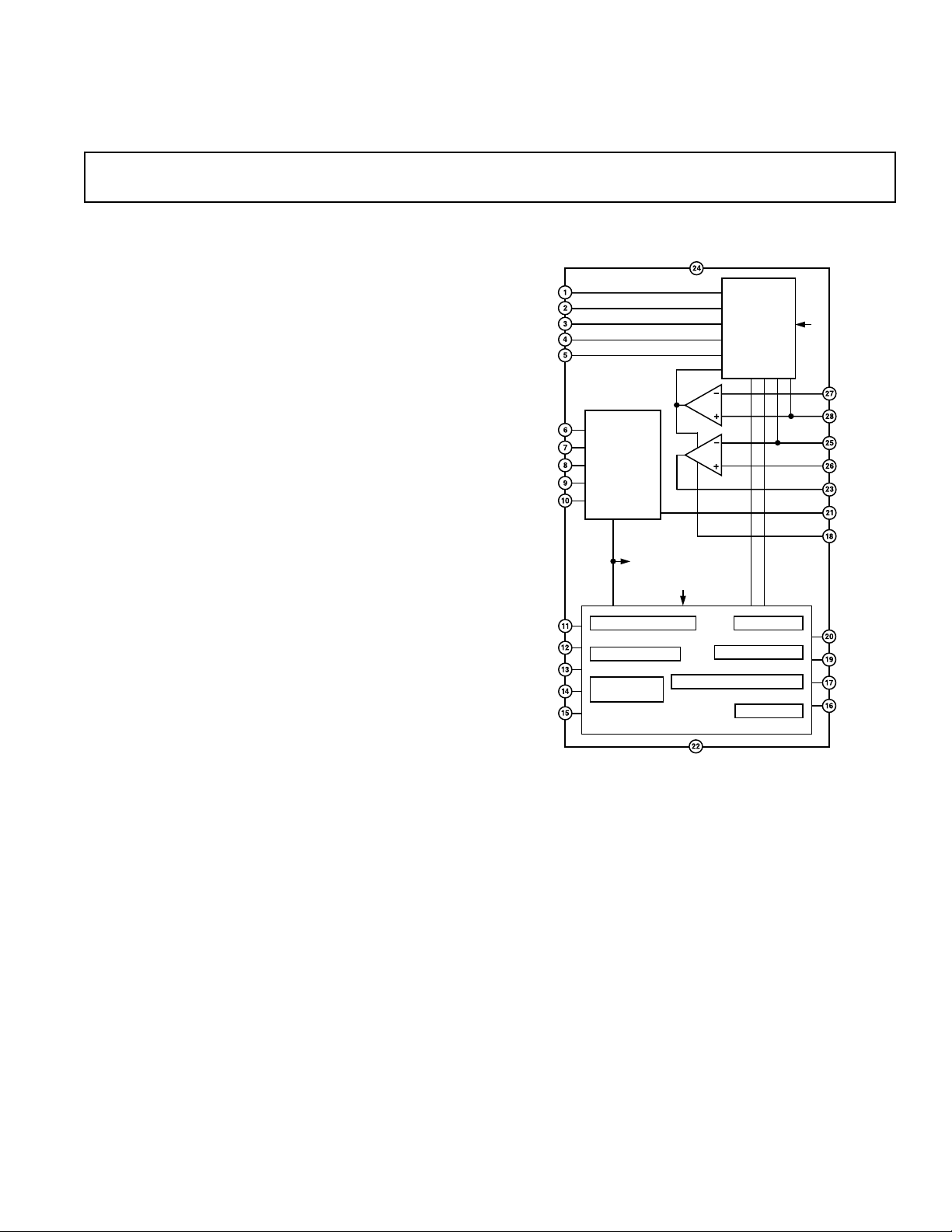
FUNCTIONAL BLOCK DIAGRAM
GENERAL DESCRIPTION
The ADP3422 is a hysteretic dc-dc buck converter controller to
power a mobile processor’s core. The optimized low voltage
design is powered from the 3.3 V system supply. The output
voltage is set by a 5-bit VID code. To accommodate the transition
time required by the newest processors for on-the-fly VID
changes, the ADP3422 features high-speed operation to allow a
minimized inductor size that results in the fastest change of
current to the output. To further allow for the minimum number
of output capacitors to be used, the ADP3422 features active
voltage positioning that can be optimally compensated to ensure a
superior load transient response. The output signal interfaces
with the ADP3415 MOSFET driver that is optimized for high
speed and high efficiency for driving both the upper and lower
(synchronous) MOSFETs of the buck converter.
REV. 0
Information furnished by Analog Devices is believed to be accurate and
reliable. However, no responsibility is assumed by Analog Devices for its
use, nor for any infringements of patents or other rights of third parties that
may result from its use. No license is granted by implication or otherwise
under any patent or patent rights of Analog Devices.
One Technology Way, P.O. Box 9106, Norwood, MA 02062-9106, U.S.A.
Tel: 781/329-4700 www.analog.com
Fax: 781/326-8703 © Analog Devices, Inc., 2001
Page 2

ADP3422–SPECIFICATIONS
1
ELECTRICAL CHARACTERISTICS
( V
DACOUT
), V
REG
= V
CS–
= V
= 1.25 V, V
VID
CPUSET
(0 ≤ TA ≤ 85ⴗC, High (H) = VCC, Low (L) = 0 V, VCC = 3.3 V, SD = H, V
= 0 V, R
= 100 k⍀, C
OUT
= 10 pF, CSS = 47 nF, R
OUT
= 5 k⍀ to VCC, R
PWRGD
to VCC, HYSSET, BSHIFT, DSHIFT, and FSHIFT are open, BOM = H, DSLP = H, DPRSLP = L, SWFB = L, unless otherwise noted. Current sunk
by a pin has a positive sign, sourced by a pin has a negative sign.)
Parameter Symbol Conditions Min Typ Max Unit
SUPPLY-UVLO-SHUTDOWN
Normal Supply Current I
UVLO Supply Current I
Shutdown Supply Current I
CC
CC(UVLO)
CCSD
SD = L 1 µA
615 mA
200 µA
UVLO Threshold
VCC Rising Up, VSS = 0 V 2.95 V
VCC Falling, VSS Floating 2.7 V
50 mV
VCC/2
UVLO Hysteresis V
Shutdown Threshold (CMOS Input) V
V
CCH
V
CCL
CCHYS
SDTH
POWERGOOD
Core Feedback Threshold Voltage V
PowerGood Output Voltage V
COREFBH
PWRGD
(Open Drain Output) V
Blanking Time t
PWRGD,BLNK
0.9 V < V
V
COREFB
V
COREFB
V
COREFB
V
COREFB
V
COREFB
COREFB
2
VCC = 3.3 V 100 µs
< 1.675 V
DAC
Rising 1.12 V
Falling 1.095 V
Rising 0.88 V
Falling 0.855 V
= V
DACOUT
= 0.8 V
DACOUT
0.95 V
0 0.8 V
DAC
DAC
DAC
DAC
CC
1.145 V
1.12 V
0.905 V
0.88 V
V
SOFT-START/HICCUP TIMER
Charge/Discharge Current I
Soft-Start Enable/Hiccup V
SS
SSEN
Termination Threshold V
Soft-Start Termination/Hiccup V
SSTERM
Enable Threshold V
VSS = 0.5 V –16 µA
= 0.5 V, VCC = 2.5 V 0.6 µA
V
SS
V
= 1.25 V,
REG
= V
RAMP
Falling 150 200 mV
V
SS
V
Rising 200 mV
SS
V
= V
RAMP
Rising 2.05 V
SS
COREFB
COREFB
= 1.27 V
= 1.27 V
VSS Falling 2.0 V
VID DAC
VID Input Threshold (CMOS Inputs) V
VID Input Current I
VID0...4
VID0...4
VID 0...4 = L 10 40 µA
0.8 0.7 V
(Internal Active Pull-up)
Output Voltage V
Output Voltage Accuracy ⌬V
Output Voltage Settling Time
3
t
DACS
DAC
DAC/VDAC
4
See VID Code Table 1 0.600 1.750 V
–0.85 +0.85 %
1.3 µs
CORE COMPARATOR
Input Offset Voltage V
Input Bias Current I
Output Voltage V
Propagation Delay Time
Rise and Fall Time
3
2
Blanking Time t
COREOS
REG
OUT_H
V
OUT_L
t
RMPOUT_PD
6
t
OUT_R
6
t
OUT_F
BLNK
V
= 1.25 V ±1.5 mV
REG
V
REG
= V
= 1.25 V ±0.3 µA
RAMP
VCC = 3.0 V 2.5 3.0 V
VCC = 3.6 V 0 0.4 V
5
50 ns
310 ns
310 ns
OUT L-H Transition 75 ns
OUT H-L Transition 140 ns
Switch Feedback Threshold V
SWFB_TH
VCC/2 V
(CMOS Input)
COREFB
CLAMP
CC
= V
DAC
= 5.1 k⍀
DAC
DAC
DAC
DAC
CC
V
V
V
V
V
V
–2–
REV. 0
Page 3

ADP3422
Parameter Symbol Conditions Min Typ Max Unit
HYSTERESIS SETTING
Hysteresis Current I
Hysteresis Reference Voltage V
SHIFT SETTING
Battery-Shift Current I
Battery-Shift Reference Voltage V
DeepSleep-Shift Current I
DeepSleep-Shift Reference Voltage V
CPU-FID-Shift Current I
CPU-FID-Shift Reference Voltage V
SHIFT CONTROL INPUTS
BOM Threshold V
(CMOS Input)
DSLP Threshold V
(IO-Level CMOS Input)
DPRSLP Mode Threshold V
(CMOS Input)
CURRENT LIMIT COMPARATOR
Input Offset Voltage V
Input Bias Current I
Hysteresis Current I
Propagation Delay Time t
RAMP_H
HYSSET
RAMPB
BSHIFT
RAMPD
DSHIFT
RAMPF
FSHIFT
BOM
DSLP
DPRSLP
CLIMOS
CS+
CS–
5
CLPD
V
= 1.25 V
REG
V
I
V
I
I
V
I
I
V
I
I
V
I
I
= V
COREFB
HYSSET
RAMP
HYSSET
HYSSET
RAMP
HYSSET
HYSSET
RAMP
HYSSET
HYSSET
RAMP
HYSSET
HYSSET
DAC
= 0 ±1 µA
= 1.23 V, BOM = H
= –10 µA +8 +10 +12 µA
= –100 µA +89 +100 +111 µA
= 1.27 V, BOM = H
= –10 µA –8 –10 –12 µA
= –100 µA –89 –100 –111 µA
= 1.23 V, BOM = L
= –10 µA +6.4 +8 +9.6 µA
= –100 µA +71 +80 +89 µA
= 1.27 V, BOM = L
= –10 µA –6.4 –8 –9.6 µA
= –100 µA –71 –80 –89 µA
1.61 1.7 1.79 V
V
= 1.25 V –92.5 –100 –107.5 µA
VID
I
= –100 µA, BOM = L
BSHIFT
DSLP = H, V
V
= 1.25 V –92.5 –100 –107.5 µA
VID
= –100 µA, BOM = H
I
DSHIFT
DSLP = L, V
V
= 1.25 V –92.5 –100 –107.5 µA
VID
I
= –100 µA, BOM = L
FSHIFT
DSLP = H, V
CPUSET
CPUSET
CPUSET
= 0 V
= 0 V
= 2 V
V
V
V
DAC
DAC
DAC
V
V
V
VCC/2 V
0.9 V
VCC/2 V
V
= 1.25 V ±0.2 ±6mV
CS–
V
= 1.25 V –0.3 µA
CS+
V
V
V
V
V
V
= V
COREFB
= V
REG
CS+
CS+
CS+
CS+
CS–
I
HYSSET
= 1.23 V BOM = H
I
HYSSET
I
HYSSET
= 1.27 V, BOM = H –1.5 –3 µA
I
HYSSET
I
HYSSET
= 1.23 V, BOM = L
I
HYSSET
I
HYSSET
= 1.27 V, BOM = L
I
HYSSET
I
HYSSET
= 1.23 V
RAMP
= 1.25 V
= 0 –0.6 –3 µA
= –10 µA –27 –31.5 –36 µA
= –100 µA –270 –301.5 –333 µA
= –10 µA –18 –21.5 –25 µA
= –100 µA –180 –201.5 –223 µA
= –10 µA –21 –25.5 –30 µA
= –100 µA –226 –241.5 –267 µA
= –10 µA –14 –17.5 –21 µA
= –100 µA –144 –161.5 –179 µA
65 ns
REV. 0
–3–
Page 4

ADP3422–SPECIFICATIONS
(continued)
Parameter Symbol Conditions Min Typ Max Unit
LOW-SIDE DRIVE CONTROL
Output Voltage (CMOS Output) V
Output Current I
DRVLSD
DRVLSD
DPRSLP = H 0.4 V
DPRSLP = L 0.7 V
V
DRVLSD
= 1.5 V
CC
V
CC
V
DPRSLP = L +0.4 mA
DPRSLP = H –0.4 mA
OVER/REVERSE VOLTAGE
PROTECTION
Over-Voltage Threshold V
COREFB,OVPVCOREFB
V
Reverse-Voltage Threshold V
COREFB,RVPVCOREFB
V
Output Current (Open Drain Output) I
CLAMP
V
V
V
NOTES
1
All limits at temperature extremes are guaranteed via correlation using standard Statistical Quality Control (SQC) methods.
2
Two test conditions:
1. PWRGD is OK but forced to fail by applying an out-of-the-CoreGood-window voltage (V
after the moment that BOM or DPRSLP is asserted/deasserted. PWRGD should not fail immediately, only with the specified blanking delay time.
2. PWRGD is forced to fail (V
BOM or DPRSLP is asserted/deasserted. PWRGD should not go high immediately, only with the specified blanking delay time.
3
Guaranteed by characterization.
4
Measured from 50% of VID code transition amplitude to the point where V
5
40 mV p-p amplitude impulse with 20 mV overdrive. Measured from the input threshold intercept point to 50% of the output voltage swing.
6
Measured between the 30% and 70% points of the output voltage swing.
Specifications subject to change without notice.
COREFB,BAD
= 1.0 V at V
= 1.25 V setting) but gets into the CoreGood-window (V
VID
Rising 2.0 2.2 V
Falling 1.8 V
COREFB
Falling –0.3 V
Rising –0.05 V
COREFB
= 1.5 V
CLAMP
= 2.2 V 10 µA
COREFB
COREFB
DACOUT
= V
settles within ± 1% of its steady state value.
= 1.25 V 1 4 mA
DACOUT
COREFB,BAD
= 1.0 V at V
= 1.25 V setting) to the COREFB pin right
VID
COREFB,GOOD
= 1.25 V) right after the moment that
–4–
REV. 0
Page 5
ADP3422
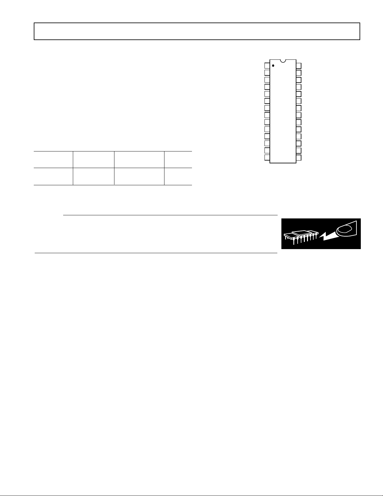
ABSOLUTE MAXIMUM RATINGS*
PIN CONFIGURATION
Input Supply Voltage (VCC) . . . . . . . . . . . . . . –0.3 V to +7 V
UVLO Input Voltage . . . . . . . . . . . . . . . . . . . . –0.3 V to +7 V
All Other Inputs/Outputs . . . . . . . . . –0.3 V to (VCC + 0.3 V)
Operating Ambient Temperature Range . . . . . . . 0°C to 85°C
Junction Temperature Range . . . . . . . . . . . . . . . 0°C to 150°C
. . . . . . . . . . . . . . . . . . . . . . . . . . . . . . . . . . . . . . . 98°C/W
θ
JA
Storage Temperature Range . . . . . . . . . . . . –65°C to +150°C
Lead Temperature (Soldering, 10 sec) . . . . . . . . . . . . 300°C
*This is a stress rating only; operation beyond these limits can cause the device to
be permanently damaged.
ORDERING GUIDE
Temperature Package Package
HYSSET
CPUSET
FSHIFT
DSHIFT
BSHIFT
VID4 (MSB)
VID3
VID2
VID1
VID0 (LSB)
BOM
DSLP
DPRSLP
PWRGD
1
2
3
4
5
6
ADP3422
7
TOP VIEW
(Not to Scale)
8
9
10
11
12
13
14
Model Range Description Option
ADP3422JRU 0°C to 85°C Thin Shrink Small RU-28
Outline (TSSOP)
CAUTION
ESD (electrostatic discharge) sensitive device. Electrostatic charges as high as 4000 V readily
accumulate on the human body and test equipment and can discharge without detection. Although
the ADP3422 features proprietary ESD protection circuitry, permanent damage may occur on
devices subjected to high-energy electrostatic discharges. Therefore, proper ESD precautions are
recommended to avoid performance degradation or loss of functionality.
28
CS–
CS+
27
REG
26
RAMP
25
VCC
24
23
OUT
GND
22
21
DACOUT
20
COREFB
SS
19
18
SWFB
17
DRVLSD
16
CLAMP
15
SD
WARNING!
ESD SENSITIVE DEVICE
REV. 0
–5–
Page 6

ADP3422
PIN FUNCTION DESCRIPTIONS
Pin No. Mnemonic Function
1 HYSSET Hysteresis Set. This is an analog I/O pin whose output is a voltage reference and whose input is a
current that is programmed by an external resistance to ground. The current is used in the IC to set
the hysteretic currents for the Core Comparator and the Current Limit Comparator. Modification of the
resistance will affect both the hysteresis of the feedback regulation and the current limit set point and
hysteresis. The application circuit suggests a resistor divider, as this pin’s functionality is used to supply a
divided reference voltage to another high-impedance pin.
2 CPUSET CPU Set. This is a high-impedance analog input pin to which a reference voltage is applied via a
resistor divider (e.g., from the HYSSET pin). The applied reference to this pin sets a threshold that
lies between two VID codes, each of which represents the Battery Optimized Mode (BOM) VID code
of a certain CPU. At startup of the CPU regulator, the BOM VID code is received and the corresponding
DACOUT voltage is compared against the CPUSET voltage. The type of CPU is then categorized
as being in one of two frequency categories, the lower of which has a lower BOM VID code. The
information is latched into the IC and, if the lower frequency CPU has been detected, is used to add
a downward shift of the regulated core voltage to the optimum level. The shift is performed using the
FSHIFT and RAMP pins.
3 FSHIFT Frequency Shift. This is an analog I/O pin whose output is a voltage reference and whose input is a
current that is programmed by an external resistance to ground. The current is used in the IC to
set a switched bias current out of the RAMP pin, depending on whether it is activated by the
latched function of the CPUSET pin. When activated, this added bias current creates a downward
shift of the regulated core voltage to a predetermined optimum level for regulation corresponding
to the frequency range of the CPU.
4 DSHIFT Deep Sleep Shift. This is an analog I/O pin whose output is a voltage reference and whose input is a
current that is programmed by an external resistance to ground. The current is used in the IC to
set a switched bias current out of the RAMP pin, depending on whether it is activated by the DSLP
signal. When activated, this added bias current creates a downward shift of the regulated core voltage
to a predetermined optimum level for regulation corresponding to Deep Sleep mode of CPU operation.
5 BSHIFT Battery Optimized Mode Shift. This is an analog I/O pin whose output is a voltage reference and
whose input is a current that is programmed by an external resistance to ground. The current is
used in the IC to set a switched bias current out of the RAMP pin, depending on whether it is activated by
the BOM signal. When activated, this added bias current creates a downward shift of the regulated core
voltage to a predetermined optimum level for regulation corresponding to Battery Optimized Mode of
CPU operation.
6 VID4 VID Input. Most significant bit.
7 VID3 VID Input
8 VID2 VID Input
9 VID1 VID Input
10 VID0 VID Input. Least significant bit.
11 BOM Battery Optimized Mode (active low). This is a digital input pin coming from a system signal
corresponding to Battery Optimized Mode of the CPU operation in its active low state and Performance
Optimized Mode (POM) in its disactivated high state. The signal controls the optimal positioning
of the core voltage regulation level according to the functionality of the BSHIFT and RAMP pins.
It is also used to initiate a blanking period for the PWRGD signal (to disable its response to a pending
dynamic core voltage change according to the VID code) whenever a signal transition occurs.
12 DSLP Deep Sleep Mode (active low). This is a digital input pin coming from a system signal which, in
its active state, corresponds to Deep Sleep mode of the CPU, which is a subset operating mode of
either BOM or POM operation. The signal controls the optimal positioning of the core voltage regulation
level according to the functionality of the DSHIFT and RAMP pins.
–6–
REV. 0
Page 7

ADP3422
Pin No. Mnemonic Function
13 DPRSLP Deeper Sleep Mode (active high). This is a digital input pin coming from a system signal corresponding to
Deeper Sleep mode of the CPU operation in its active high state. It is used to initiate a blanking period
for the PWRGD signal (to disable its response to a pending dynamic core voltage change according to the
VID code) whenever a signal transition occurs.
14 PWRGD Power Good (active high). This is an open drain output pin which, via the assistance of an external
pull-up resistor, indicates that the core voltage is within the specified tolerance of the VID programmed
value or else in a VID transition state as indicated by a recent state transition of either the BOM or
DPRSLP pins. PWRGD is deactivated (pulled low) when the IC is disabled or in UVLO mode or
soft-start. The open drain output allows external ORing with other open drain/collector powergood indicators.
15 SD Shutdown (active low). This is a digital input pin coming from a system signal which, in its active
state, shuts down the IC operation, placing the IC in its lowest quiescent current state for maximum
power savings.
16 CLAMP Clamp (active high). This is an open drain output pin which, via the assistance of an external pull-up
resistor, indicates that the core voltage should be clamped for its protection. To allow the highest
level of protection, the CLAMP signal is developed using both a redundant reference and a redundant feedback path with respect to those of the main regulation loop. It is also latched. In a
preferred and more conservative configuration, the core voltage is clamped by an external FET.
The initial protection function is served when it is activated by detection of either an overvoltage or a
reverse-voltage condition on the COREFB pin. A backup protection function due to loss of the
latched signal at IC power-off is served by connecting the pull-up resistor to a system “ALWAYS”
regulator output (e.g., V5_ALWAYS). If the external FET is used, this implementation will keep the
core voltage clamped until the ADP3422 has power reapplied, thus keeping protection for the
CPU even after a hard-failure power-down and restart (e.g., a shorted top FET).
17 DRVLSD Drive-Low Shutdown (active low). This is a digital output pin which, in its active state, indicates that
the lower FET of the core VR should be disabled. In the suggested application schematic this pin is
directly connected to the pin of the same name on the ADP3415 or other driver IC. The pin is normally
asserted in the light load condition, but its assertion will be deactivated by the consideration of a
number of dynamic conditions where operation of the lower FET may be needed.
18 SWFB Switched Node Feedback. This is a high-impedance analog input pin that is used to allow the
ON-time noise blanking function to terminate earlier than its internally preset time by its indication
that the turn-ON of the upper FET has occurred. A resistor must be inserted between the pin and the
switched node of the core VR so that the input can be clamped (at ~7V) and is not exposed to
high voltage. This pin can also be shorted to ground if the need for this speed enhancement is
deemed unnecessary.
19 SS Soft Start. This is an analog I/O pin whose output is a controlled current source used to charge or
discharge an external grounded capacitor and whose input is the detected voltage that is indicative of
elapsed time. The pin controls the soft start time of the IC as well as the hiccup cycle time during
short circuit. Hiccup operation is a feature that was added to reduce short circuit power dissipation by
more than an order of magnitude, while still allowing an automatic restart when the short is removed.
20 COREFB Core Feedback. This is a high-impedance analog input pin that is used to monitor the output voltage
for setting the proper state of the PWRGD and CLAMP pins. It is generally recommended to
RC-filter the noise from the monitored core voltage, as suggested by the application schematic.
21 DACOUT VID-Programmed Digital-to-Analog Converter Output. This voltage is the reference voltage for output
voltage regulation.
22 GND Ground
23 OUT Driver Command Output Signal. This is a digital output pin which is used to command the state of the
switched node via the driver. It should be connected to the IN pin of the ADP3415 or similar driver.
24 VCC Power Supply
REV. 0
–7–
Page 8

ADP3422
Pin No. Mnemonic Function
25 RAMP Regulation Ramp Feedback Input. This is a high-impedance analog input pin which is used for providing
negative feedback of the hysteretically-controlled output. Several switched current sources also
appear at this input, most notably the cycle-by-cycle hysteresis-setting switched current programmed by
the HYSSET pin. The external resistive termination at this pin sets the magnitude of the hysteresis
applied to the regulation loop.
26 REG Regulation Voltage Summing Input. This is a high-impedance analog input pin into which the voltage
reference of the feedback loop allows the summing of both the DACOUT voltage and the core voltage for
programming the output resistance of the core voltage regulator. This is also the pin at which an optimized
transient response can be tailored using Analog Devices’ patented ADOPT™ design technique.
27 CS+ Current Limit Positive Sense. This is a high-impedance analog input pin that is normally connected to the
positive node of the current sense resistor.
28 CS– Current Limit Negative Sense. This is a high-impedance analog input pin that is normally connected via
a current-limit programming resistor to the negative node of the current sense resistor. A hystereticallycontrolled current—three times the current programmed at the HYSSET pin—flows out of this pin
and develops a current-limit-setting voltage across that resistor. This voltage must be exceeded by the
inductor current generated current sense voltage in order to trigger the current limit function. When it is
triggered, the current flowing out of this pin is reduced—to two-thirds of its previous value—producing
hysteresis in the current limit operation.
ADOPT is a trademark of Analog Devices, Inc.
–8–
REV. 0
Page 9

10000
100
–100
020
HYSTERESIS CURRENT – A
40 60 80 100
0
OUT = HIGH, RHYS = 17k⍀
OUT = HIGH, RHYS = 170k⍀
OUT = LOW, RHYS = 170k⍀
OUT = LOW, RHYS = 17k⍀
TEMPERATURE – ⴗC
100
0.01
0.1 1 10 100
1
10
0.1
TIMING CAPACITANCE – nF
SOFT-START TIME – ms
NORMAL OPERATING MODE
1000
100
UVLO MODE
10
Typical Performance Characteristics–ADP3422
SUPPLY CURRENT – A
1
SHUTDOWN MODE
0.1
0 10020
40 60 80
TEMPERATURE – ⴗC
TPC 1. Supply Current vs. Temperature
1.765
1.750
1.735
0.605
DAC OUTPUT – V
0.600
0.595
0 10020
+0.85%
FULL SCALE
–0.85%
+0.85%
ZERO SCALE
–0.85%
40 60 80
AMBIENT TEMPERATURE – ⴗC
TPC 2. DAC Output Voltage vs. Temperature
TPC 4. Core Hysteresis Current vs. Temperature
0
–50
OUT = LOW, R
–100
–150
–200
OUT = LOW, R
– PIN CURRENT – A
L
–250
C
–300
OUT = HIGH, R
–350
020
TPC 5. Current Limit Programming Current
vs. Temperature
= 170k⍀
HYSSET
HYSSET
HYSSET
OUT = HIGH, R
= 17k⍀
= 17k⍀
40 60 80 100
TEMPERATURE – ⴗC
HYSSET
= 170k⍀
HIGH
POWER GOOD
LOW
–15 15–10 –5510
TPC 3. Power Good vs. Relative Core Voltage Variation
REV. 0
RELATIVE CORE VOLTAGE – %
0
TPC 6. Soft-Start Time vs. Timing Capacitance
–9–
Page 10

ADP3422
APPLICATION INFORMATION
This application section presents both the theoretical background
and the detailed procedure for designing dc/dc converters with
the ADP3422 controller for mobile CPUs. The ADP3422 is
used in a unique ripple regulator (also called hysteretic regulator)
configuration, which allows employing ADOPT, Analog Devices’
optimal voltage positioning technique to implement the output
desired voltage impedance statically and dynamically, as required
by Intel’s IMVP-2 specification.
Hysteretic Regulator
Figure 1 shows the conventional hysteretic regulator and the
characteristic waveforms. The operation is as follows. During
the time the upper transistor, Q1, is turned on, the inductor
current, I
V
OUT
, and also the output voltage, V
L
reaches the upper threshold of the hysteretic comparator,
, increase. When
OUT
Q1 is turned off, Q2 is turned on, and the inductor current and also
the output voltage begin to decrease. The cycle repeats after
reaches the lower threshold of the hysteretic comparator.
V
OUT
V
IN
Q1
Q2
V
H
L
I
V
L
V
SW
C
R
V
REF
OUT
O
E
LOAD
V
OUT
V
H
V
SW
I
L
Figure 1. Conventional Hysteretic Regulator and Its
Characteristic Waveforms
The switching frequency is determined by the equivalent series
resistance R
of the output capacitor, the inductance L of the
E
inductor, the input and output voltages, and the hysteresis
V
of the comparator. It is as follows:
H
RLVVVV
( – )
EHIN OUT OUT
f
=
V
IN
(1)
Since there is no voltage-error amplifier in the hysteretic regulator,
its response to any change in the load current or the input voltage is virtually instantaneous. Therefore, the hysteretic regulator
represents the fastest possible dc/dc converter control technique.
A slight disadvantage of the hysteretic regulator is that its frequency
varies with the input and output voltages. In a typical mobile CPU
converter application, the worst-case frequency variation due to
the input voltage variation is in the order of 30%, which is usually acceptable. In the simplest implementation of the hysteretic
converter, shown in Figure 1, the frequency also varies proportionally with the ESR of the output capacitor. Since the initial value
is often poorly controlled, and the ESR of electrolytic capacitors
also changes with temperature and age, practical ESR variations
can easily lead to a frequency variation on the order of three to
one. However, using the ADP3422 controller in a modified
hysteretic topology eliminates the dependence of the operating
frequency on the ESR. In addition, the modification allows the
optimal implementation, ADOPT, of the Intel’s IVMP-2 load-line
specification. Figure 2 shows the modified hysteretic regulator.
V
IN
Q1
Q2
V
H
L
I
R
L
CS
C
OC
R
C
R
D
V
OUT
C
O
LOAD
R
E
V
REF
Figure 2. Modified Hysteretic Regulator with ADOPT
The implementation requires adding a resistive divider (RC and
) between the reference voltage and the output, and connecting
R
D
the tap of the divider to the noninverting input of the hysteretic
comparator. A capacitor, C
) of the divider.
ber (R
C
, is placed across the upper mem-
OC
It is easily shown that the output impedance of the converter can
be no less than the ESR of the output capacitor. A straightforward derivation demonstrates that the output impedance of the
converter in Figure 2 can be minimized to equal the ESR, R
,
E
when the following two equations are valid (neglecting PCB
trace resistance for now):
RRRR
DCECS
–
=
R
CS
(2)
and
2
CR
OC
=
RR
OE
CS D
(3)
C
From (3), the series resistance is:
R
R
CS
E
=
R
D
+1
R
C
(4)
This is the ADOPT configuration and design procedure that
allows the maximum possible ESR to be used while meeting a
given load-line specification.
It can be seen from (4) that unless R
R
will be always smaller than RE. An advantage of the circuit
CS
of Figure 2 is that if we select the ratio R
the additional dissipation introduced by the series resistance R
is zero or RC is infinite,
D
well above unity,
D/RC
CS
will be negligible. Another interesting feature of the circuit in
Figure 2 is that the ac voltage across the two inputs of the hysteretic comparator is now equal only to the ac voltage across
. This is due to the presence of the capacitor COC, which
R
CS
effectively couples the ac component of the output voltage to the
noninverting input voltage of the comparator. Since the comparator sees only the ac voltage across R
, in the circuit of
CS
Figure 2 the dependence of the switching frequency on the ESR
of the output capacitor is completely eliminated. Equation (5)
presents the expression for the switching frequency.
RLVVV V
( – )
CSHIN OUT OUT
f
=
V
IN
(5)
–10–
REV. 0
Page 11

7V–21V
V_DC
C23
C22
C21
C20
C19
C18
C17
ADP3422
C33
CORE
V
C32
C31
C30
C29
C28
C27
150F
150F
150F
150F
150F
150F
150F
10F
10F
10F
10F
10F
10F
0.1F
L1
0.66H
CS
R
D1
V_5S
BAR43S
C3
C2
C1
C12
0.1F
1000pF
0.1F
10F
C16
0.1F
C15
0.1F
10
BST
ADP3415
IN
12345
Q2
Q1
IR7807V IR7807V
987
SW
DRVH
SD
DRVLSD
CORE_ON
D2
D3
GND
DLY
6
DRVL
VCC
R7
Q3 Q4 Q5
IR7811W IR7811W IR7811W
V_3S
CSF
CSF
R
C
A
R
CL
R
C
OC
R
C
D
R
C8
R6
2.7⍀
28272625242322212019181716
CS–
C4
10pF
CS+
REG
C5
10pF
RAMP
VCC
C6
OUT
R9
C9
10nF
1F
47nF
0.1F
GND
DACOUT
COREFB
C26
C25
C24
V_5 ALWAYS
C10
R12
SS
150F
150F
150F
Q6
IR7807V
R15
5.1k⍀
10k⍀
CLAMP
DRVLSD
CORE_ON
15
SD
SS
C
SWFB
REV. 0
ADP3422
HYSSET
CPUSET
FSHIFT
234
DSHIFTRBSHIFT
FSHIFT
R
R
DSHIFT
SET2
R
SET1
R
1
Figure 3. Application Circuit
–11–
BSHIFT
VID4
VID3
VR_VID4
VR_VID3
VID2
VR_VID2
56789
VID1
VID0
BOM
1011121314
VR_VID1
VR_VID0
GMUXSEL
DSLP
DPRSLP
DPSLP
DPRSLPVR
PWRGD
V_3S
R19
5.1k⍀
Page 12

ADP3422
Application Schematic
Figure 3 shows the simplified application schematic of the
ADP3422 control IC. The ADP3422, together with its companion dual MOSFET driver IC, the ADP3415, controls a
hysteretic converter that generates the core voltage for the CPU.
Design Procedure—Power Stage Components
The first step of the converter design is to select the MOSFETs
to be used based on acceptable dc and switching losses. For this
selection, the designer is referred to the MOSFET manufacturers who may provide not only a recommendation for the
MOSFETs to be used for the specific application, but also
data and/or guidelines for determining an acceptable maximum operating frequency.
With this information, the next step is to choose an inductance
value—usually the smallest available value, that will yield an
acceptable ripple current. A ripple current 30%~60% of the
maximum core current is recommended. Inductance, frequency,
and ripple current are related by formula (6), derived from (5):
L
1(– )
=
fI
MAX RPP
IM VID VID
V
IM
(6)
VVV
where:
L = inductance value
f
= maximum acceptable switching frequency
MAX
I
= selected peak-to-peak ripple current
RPP
V
= maximum input voltage
IM
V
= nominal programmed VID voltage
VID
Assuming f
= 1.25 V, the required inductance value is L = 729 nH.
V
VID
= 250 kHz, I
MAX
= 8 A, VIM = 20 V, and
RPP
A standard value of 660 nH is available.
The next step is to select the current sensing resistor, R
CS
. The
restrictions are that (1) the resistance should not be higher than
the core converter output impedance defined by Intel’s IMVP-2
specification, and (2) the resistance should not be so low that
the errors in reading the current sense signal become a problem.
The IMVP-2 specification requires that the converter output
impedance, R
, be 4 mΩ. An RCS value of above one-quarter
OUT
of the nominal output impedance provides sufficient protection
against errors in the current sense signal. The chosen value is
= 1.5 mΩ.
R
CS
Also, the power dissipation, P
, should be calculated to ensure
CS
that a properly sized resistor is selected:
PRI
CS CS O MAX=()
where I
O(MAX)
example I
O(MAX)
2
is the maximum output current. In this design
= 19 A. The resulting dissipation of the current
(7)
sense resistor is 542 mW.
The final step in finishing the design of the power stage is selecting the output capacitors. There are two primary considerations
in choosing those capacitors. The total ESR may not exceed the
output resistance required by Intel’s IMVP-2 specification. Also
the total capacitance must be checked to make sure that it is
sufficient to prevent overshoot beyond the voltage step caused
by the ESR during a full load transient, according to the formula:
LI I
( – )
×
O MAX O MIN
C
OMIN
()
=
where I
is the minimum rated current for the normal
O(MIN)
operation region of the CPU where I
() ()
RV
×
OUT L
O(MAX)
(8)
can occur, and VL is
the voltage applied across the inductor in order to ramp the
current in the direction of the load step. The minimum CPU
voltage represents a critical performance limit that must not be
violated during a load step increase. Therefore, the minimum
capacitance must never be less than the calculated value when
using V
= V
L
I(MIN)
– V
in (8) the voltage applied across the
VID
inductor to ramp up the current. However, overshoot would still
occur unless the capacitance is greater than the calculated value
= V
when using V
L
in (8). The magnitude of the overshoot is
VID
given by:
L
V
OS
I
=+
O MAX
C
O
I
RPP
() () ()
2
2
–––
22
+
IVRIV
O MIN VID OUT O MAX VID
[]
(9)
For this design example, output capacitors with a capacitance
of 150 µF and a maximum ESR of 20 mΩ are chosen. Given
the target of R
= 4 mΩ, five capacitors would be needed to
OUT
achieve a total ESR of not more than 4 mΩ. The total capacitance of five of these capacitors is 750 µF. This capacitance is
greater than the value required for a load step increase, even
for an input voltage as low as 6 V; but it is less than what is
needed to prevent an overshoot for a load step decrease, where
only the output voltage is applied across the inductor to ramp
down the current to the minimum value. Assuming that the
minimum current is zero, the overshoot above V
is 89 mV.
VID
Design Procedure—Control Circuit Components
The output resistance is implemented by using the proper ratio
of two resistors, which connect to the REG pin. One resistor,
, connects to the DAC reference and the other, RC, connects
R
D
to the core voltage. From (2):
RRRRR
DCET CS
where R
––
=
R
CS
is the PCB trace resistance between the current sense
T
(10)
resistor and the CPU measurement point.
There is no inherent restriction on the absolute value of either
R
or RC, but values in the single kΩ range are recommended.
D
These resistors can now be selected.
–12–
REV. 0
Page 13

ADP3422
A capacitor is required across RC to achieve optimal compensation.
This ensures that the output voltage does not bounce back temporarily right after a load transient, i.e., the output impedance of
the converter is purely resistive. The bounce-back is undesirable
because it increases the peak-to-peak deviation in the output
voltage. From (3), the optimal capacitance value is:
CR
OC
=
RR
OE
CD
value should be selected as close to
OC
(11)
C
At this point, the exact C
the calculated one as possible. It is generally recommended to
choose the nearest value of C
is calculated. Optionally, C
the values of R
and RC can be reselected to satisfy the previous
D
which is not greater than what
OC
can be chosen first arbitrarily and
OC
two equations.
The output impedance is now set.
The next step in the design is to determine the value of the
hysteresis-setting resistor, R
current. R
connects between the RAMP pin and RCS on the
A
, which sets the inductor ripple
A
inductor side and is determined by:
R
A
where t
IR Vt RL
RPP CS IM D OFF CS
=
D(OFF)
– /
I
2
()
H
(12)
is the turn-off delay time of the power converter,
including delays through the ADP3422, ADP3415, and the
external MOSFETs, and I
is a user-programmed current set
H
by a resistor on the ADP3422’s HYSSET pin, which sets the
current that is hysteretically switched in and out of the RAMP
pin. Assuming a turn-off delay of 50 ns and a hysteresis-setting
current of 30 µA, the calculated value of R
is 162 Ω.
A
To protect the converter, the hysteretic current limiting should
be set. The current limit programming resistor, R
, which
CL
connects between the CS– pin and the core output is given by:
kR I I
R
I CS O MAX RPP
=
CL
where k
is a margin factor for the current limit setting. A
I
typical value for k
I
+(/)
()
I
3
H
2
(13)
might be 1.15, which would set the current
limit point 15% above the maximum rated core current. Using
the preceding design target values, a value of 441 Ω for R
CL
is
calculated.
In order to optimize the power savings by always using the
minimum allowed CPU supply voltage, the IMVP-2 specification introduces two operating-mode-dependent voltage shifts.
The first shift is for optimizing the output voltage when the
battery-optimized-mode (BOM) VID code is selected. The
shift is achieved by connecting a resistor, R
BSHIFT
, between
the BSHIFT pin and ground. The shift will be used whenever
the BOM pin is driven low, indicating that the BOM VID
code is selected. The shift is given by:
V
BSHIFT
R
–
A
BSHIFT
V
VID BOM
=+
R
R
D
1
,
R
C
(14)
The second shift is for optimizing the output voltage when the
Deep Sleep operating mode is selected in conjunction with
either the POM or BOM VID codes. This shift is achieved by
connecting a resistor, R
, between the DSHIFT pin and
DSHIFT
ground. The shift will be used whenever the DPSLP pin is
driven low. The shift is given by:
V
DSHIFT
–
R
A
DSHIFT
V
VID BOM
=+
R
R
D
1
,
R
C
(15)
PRINTED CIRCUIT BOARD LAYOUT
CONSIDERATIONS
The following guidelines are recommended for optimal performance of the ADP3422 and ADP3415 in a power converter.
The circuitry is considered in three parts: the power switching
circuitry, the output filter, and the control circuitry.
Placement Overview
1. For ideal component placement, the output filter capacitors
will divide the power switching circuitry from the control
section. As an approximate guideline, considered on a
single-sided PCB, the best layout would have components
aligned in the following order: ADP3415, MOSFETs and
input capacitor, output inductor, current sense resistor, output
capacitors, control components and ADP3422. Note that
the ADP3422 and ADP3415 are completely separated for
an ideal layout, which is only possible with a two-chip solution.
This will minimize jitter in the control caused by having the
driver and MOSFETs close to the control and give more
freedom in the layout of the power switching circuitry.
2. Whenever a power dissipating component (e.g., a power
MOSFET) is soldered to a PCB, the liberal use of vias, both
directly on the mounting pad and immediately surrounding
it, is recommended. Two important reasons for this are:
improved current rating through the vias (if it is a current
path), and improved thermal performance—especially if
the vias extend to the opposite side of the PCB where a
plane can more readily transfer heat to air.
Power Switching Circuitry
ADP3415, MOSFETs, and Input Capacitors
3. Locate the ADP3415 near the MOSFETs so the parasitic
inductance in the gate drive traces and the trace to the SW
pin is small, and so that the ground pins of the ADP3415
are closely connected to the lower MOSFET’s source.
4. Locate at least one substantial (i.e., > ~10 µF) input bypass
MLC capacitor close to the MOSFETs so that the physical
area of the loop enclosed in the electrical path through the
bypass capacitor and around through the top and bottom
MOSFETs (drain-source) is small. This is the switching
power path loop.
5. Make provisions for thermal management of all the
MOSFETs. Heavy copper and wide traces to ground and
power planes will help to pull the heat out. Heat sinking
by a metal tap soldered in the power plane near the
MOSFETs will help. Even just small airflow can help
tremendously. Paralleled MOSFETs will help spread the
heat, even if the on-resistance is higher.
REV. 0
–13–
Page 14

ADP3422
6. An external “antiparallel” schottky diode (across the bottom
MOSFET) may help efficiency a small amount (< ~1 %); a
MOSFET with a built in antiparallel schottky is more effective. For an external schottky, it should be placed next to
the bottom MOSFET or it may not be effective at all. Also,
a higher current rating (bigger device with lower voltage
drop) is more effective.
7. The ground pin of the ADP3415 should be connected into
the power switching circuitry ground plane, and the VCC
bypass capacitor should be close to the VCC pin and connected into the same ground plane.
Output Filter
Output Inductor and Capacitors, Current Sense Resistor
8. Locate the current sense resistor very near to the output
capacitors.
9. PCB trace resistances from the current sense resistor to the
output capacitors, and from the output capacitors to the
load should be minimized, known (calculated or measured),
and compensated for as part of the design if it is significant.
(Remote sensing is not sufficient for relieving this requirement!) A square section of 1-ounce copper trace has a
resistance of ~500 mW. Using 2~3 squares of copper can
make a noticeable impact on a 15 A design.
10. Whenever high currents must be routed between PCB layers,
vias should be used liberally to create several parallel current
paths so that the resistance and inductance introduced by
these current paths is minimized and the via current rating is
not exceeded.
11. The ground connection of the output capacitors should be
close to the ground connection of the lower MOSFET and
it should be a ground plane. Current may pulsate in this
path if the power source ground is closer to the output
capacitors than the power switching circuitry, so a close
connection will minimize the voltage drop.
Control Circuitry
ADP3422, Control Components
12. If the placement overview cannot be followed, then in order
to avoid introducing ground noise from the power switching
stage into the control circuitry, the ground pin of the
ADP3422 should be Kelvin-connected into the ground plane
near the output capacitors. All other control components
should be grounded on that same signal ground.
13. If critical signal lines (i.e., signals from the current sense
resistor leading back to the ADP3422) must cross through
power circuitry, it is best if a signal ground plane can be
interposed between those signal lines and the traces of the
power circuitry. This serves as a shield to minimize noise
injection into the signals at the expense of making signal
ground a bit noisier.
14. Absolutely avoid crossing any signal lines over the switching
power path loop, described previously.
15. Accurate voltage positioning depends on accurate current
sensing, so the control signals which monitor the voltage
differentially across the current sense resistor should be
kelvin connected.
16. The RC filter used for the current sense signal should be
located near the control components.
Table I. VID Code
VID4 VID3 VID2 VID1 VID0 V
0 0 0 0 0 1.750
0 0 0 0 1 1.700
0 0 0 1 0 1.650
0 0 0 1 1 1.600
0 0 1 0 0 1.550
0 0 1 0 1 1.500
0 0 1 1 0 1.450
0 0 1 1 1 1.400
0 1 0 0 0 1.350
0 1 0 0 1 1.300
0 1 0 1 0 1.250
0 1 0 1 1 1.200
0 1 1 0 0 1.150
0 1 1 0 1 1.100
0 1 1 1 0 1.050
0 1 1 1 1 1.000
1 0 0 0 0 0.975
1 0 0 0 1 0.950
1 0 0 1 0 0.925
1 0 0 1 1 0.900
1 0 1 0 0 0.875
1 0 1 0 1 0.850
1 0 1 1 0 0.825
1 0 1 1 1 0.800
1 1 0 0 0 0.775
1 1 0 0 1 0.750
1 1 0 1 0 0.725
1 1 0 1 1 0.700
1 1 1 0 0 0.675
1 1 1 0 1 0.650
1 1 1 1 0 0.625
1 1 1 1 1 0.600
VID
–14–
REV. 0
Page 15

OUTLINE DIMENSIONS
Dimensions shown in inches and (mm).
28-Lead Thin Shrink Small Outline Package (TSSOP)
(RU-28)
0.386 (9.80)
0.378 (9.60)
ADP3422
PIN 1
0.006 (0.15)
0.002 (0.05)
SEATING
PLANE
28
0.0256 (0.65)
BSC
0.0118 (0.30)
0.0075 (0.19)
15
0.177 (4.50)
0.169 (4.30)
141
0.0433 (1.10)
MAX
0.0079 (0.20)
0.0035 (0.090)
0.256 (6.50)
0.246 (6.25)
8ⴗ
0ⴗ
0.028 (0.70)
0.020 (0.50)
REV. 0
–15–
Page 16

C01882–.8–10/01(0)
–16–
PRINTED IN U.S.A.
 Loading...